JP4448889B2 - Imaging device and imaging apparatus - Google Patents
Imaging device and imaging apparatus Download PDFInfo
- Publication number
- JP4448889B2 JP4448889B2 JP2009067933A JP2009067933A JP4448889B2 JP 4448889 B2 JP4448889 B2 JP 4448889B2 JP 2009067933 A JP2009067933 A JP 2009067933A JP 2009067933 A JP2009067933 A JP 2009067933A JP 4448889 B2 JP4448889 B2 JP 4448889B2
- Authority
- JP
- Japan
- Prior art keywords
- pixel
- imaging device
- photoelectric conversion
- pair
- wavelength selection
- Prior art date
- Legal status (The legal status is an assumption and is not a legal conclusion. Google has not performed a legal analysis and makes no representation as to the accuracy of the status listed.)
- Expired - Fee Related
Links
- 238000003384 imaging method Methods 0.000 title claims description 111
- 238000006243 chemical reaction Methods 0.000 claims description 135
- 239000003086 colorant Substances 0.000 claims description 39
- 238000012545 processing Methods 0.000 claims description 31
- 230000035945 sensitivity Effects 0.000 claims description 26
- 239000004065 semiconductor Substances 0.000 claims description 23
- 239000000758 substrate Substances 0.000 claims description 22
- 230000000295 complement effect Effects 0.000 claims description 9
- 238000012546 transfer Methods 0.000 description 49
- 238000010586 diagram Methods 0.000 description 18
- 230000006835 compression Effects 0.000 description 4
- 238000007906 compression Methods 0.000 description 4
- 230000006837 decompression Effects 0.000 description 4
- 230000004048 modification Effects 0.000 description 4
- 238000012986 modification Methods 0.000 description 4
- 230000003321 amplification Effects 0.000 description 3
- 238000012937 correction Methods 0.000 description 3
- 238000003199 nucleic acid amplification method Methods 0.000 description 3
- 238000001228 spectrum Methods 0.000 description 3
- 230000008901 benefit Effects 0.000 description 2
- 230000006870 function Effects 0.000 description 2
- 230000003287 optical effect Effects 0.000 description 2
- 230000003595 spectral effect Effects 0.000 description 2
- 230000009471 action Effects 0.000 description 1
- 230000015572 biosynthetic process Effects 0.000 description 1
- 230000000903 blocking effect Effects 0.000 description 1
- 230000006866 deterioration Effects 0.000 description 1
- 238000009792 diffusion process Methods 0.000 description 1
- 230000005484 gravity Effects 0.000 description 1
- 230000006872 improvement Effects 0.000 description 1
- 239000011159 matrix material Substances 0.000 description 1
- 238000000034 method Methods 0.000 description 1
- 230000009467 reduction Effects 0.000 description 1
- 238000003786 synthesis reaction Methods 0.000 description 1
Images


Landscapes
- Color Television Image Signal Generators (AREA)
- Solid State Image Pick-Up Elements (AREA)
Description
本発明は、複数の色のカラーフィルタを配列してなる撮像素子、及び、該撮像素子を用いてカラー画像を生成する撮像装置に関する。 The present invention relates to an imaging device in which color filters of a plurality of colors are arranged, and an imaging device that generates a color image using the imaging device.
従来のデジタルスチルカメラやデジタルビデオカメラなどの撮像装置は、例えば、複数の色を所定のカラーパターンで配列してなるカラーフィルタを備えた固体撮像素子をイメージセンサとして用いる構成を有している。カラーフィルタとしては、R(赤)、G(緑)、B(青)のフィルタを配列したものがある。カラーフィルタを有する撮像素子や撮像装置としては、例えば、下記特許文献に示すものがある。 2. Description of the Related Art Conventional imaging devices such as digital still cameras and digital video cameras have a configuration in which, for example, a solid-state imaging device including a color filter formed by arranging a plurality of colors in a predetermined color pattern is used as an image sensor. As color filters, there are filters in which R (red), G (green), and B (blue) filters are arranged. As an image pick-up element and an image pick-up device which have a color filter, there exist some shown in the following patent documents, for example.
特許文献1の撮像装置は、単板型のカラー撮像装置において、5色以上のマルチバンド用のカラーフィルタを備えた構成である。
The image pickup apparatus of
特許文献2は、波長選択性がことなる複数種類のフィルタのうち何れかのフィルタが各画素位置に割り当てられたカラーフィルタであって、カラーフィルタの色C1が市松状に配置され、他の色C2,C3,C4,C5がC1の存在しない位置にランダムに配置されている。
ところで、特許文献1の撮像装置では、6色のカラーフィルタを用いることで色再現性を向上することができるが、原色に近似される画素同士が離間している。このため、原色の情報が画素間の相関性が低くなることにより精度が落ちてしまう。また、原色に近似される画素間を利用したダイナミックレンジの拡大も同様に精度が落ちる点で改善の余地があった。
さらに、高感度撮影では画素加算が有効であるが、原色に近似される画素同士を加算すると、画素同士が離間しているため、偽信号など画質低下が発生してしまう。
By the way, in the image pickup apparatus of
Furthermore, pixel addition is effective in high-sensitivity shooting, but if pixels that are approximate to the primary color are added, the pixels are separated from each other, resulting in a reduction in image quality such as a false signal.
本発明は、上記事情に鑑みてなされたもので、その目的は、色再現性を向上させるとともに、ダイナミックレンジを拡大できる撮像素子及び撮像装置を提供することにある。 The present invention has been made in view of the above circumstances, and an object thereof is to provide an imaging device and an imaging apparatus capable of improving color reproducibility and expanding a dynamic range.
本発明の上記目的は、下記構成によって達成される。
(1)入射光に対して異なる波長選択性を有する画素部を少なくとも4種類備える撮像素子であって、
複数の前記画素部が、隣接する2種類の画素部からなる画素部対を含み、前記画素部対は異なる波長選択性を持ち、かつ、それぞれの波長選択範囲を合わせた範囲が3原色のうち1つの波長選択範囲と略同一となる異色画素部対を少なくとも1つ含み、前記画素部対ごとに加算された画素の配列がベイヤー配列となる撮像素子。
(2)入射光に対して異なる波長選択性を有する画素部を少なくとも4種類備える撮像素子であって、
複数の前記画素部が、隣接する2種類の画素部からなる画素部対を含み、前記画素部対は異なる波長選択性を持ち、かつ、それぞれの波長選択範囲を合わせた範囲が3原色のうち1つの波長選択範囲と略同一となる異色画素部対を少なくとも1つ含み、前記異色画素部対が3種類であり、該異色画素部対の波長選択範囲の和がそれぞれ3原色に対応し、全体として6種類の波長選択範囲を有する画素部を備える撮像素子。
(3)前記異なる波長選択性は波長選択範囲の中心が異なる(1)又は(2)に記載の撮像素子。
(4)前記異なる波長選択性は波長選択範囲の幅が異なる(1)又は(2)に記載の撮像素子。
(5)前記画素部対が、前記異色画素部対と、波長選択範囲の中心が同一である同色画素部対とから構成される(1)から(4)のいずれか1つに記載の撮像素子。
(6)前記画素部が、波長選択フィルタを含み、該波長選択フィルタによって該画素部の波長選択性が規定される(1)から(5)のいずれか1つに記載の撮像素子。
(7)前記画素部が、光電変換部を含み、該光電変換部によって該画素部の波長選択性が規定される(1)から(6)のいずれか1つに記載の撮像素子。
(8)前記画素部が波長選択フィルタと光電変換部を含み、波長選択フィルタと光電変換部により画素部の波長選択性が規定される(1)から(7)のいずれか1つに記載の撮像素子。
(9)前記異色画素部対となる画素同士の信号を撮像素子内で加算すること(1)から(8)のいずれか1つに記載の撮像素子。
(10)前記異色画素部対となる画素同士の信号を信号処理で加算すること(1)から(9)のいずれか1つに記載の撮像素子。
(11)半導体基板上に前記信号電荷を生成する複数の光電変換部が行方向及び列方向に配列され、前記複数の光電変換部が同一の配列ピッチで格子状に配列され、かつ、前記行方向又は前記列方向に対して約45度斜めにした配列である(1)から(10)のいずれか1つに記載の撮像素子。
(12)半導体基板上に前記信号電荷を生成する複数の光電変換部が行方向及び列方向に配列され、前記複数の光電変換部が同一の配列ピッチで格子状に配列されている(1)から(10)のいずれか1つに記載の撮像素子。
(13)前記異色画素部対を構成する画素部の感度がそれぞれ異なる(1)から(12)のいずれか1つに記載の撮像素子。
(14)前記異色画素部対に含まれる画素部と、該画素部隣接する画素部との組み合わせでそれぞれの波長選択範囲の和が、補色の少なくとも1つに対応する波長選択範囲と略同一となる(1)から(13)のいずれか1つに記載の撮像素子。
(15)入射光に対して異なる波長選択性を有する画素部を少なくとも4種類備える撮像素子備えた撮像装置であって、
複数の前記画素部が、隣接する2種類の画素部からなる画素部対を含み、前記画素部対は異なる波長選択性を持ち、かつ、それぞれの波長選択範囲を合わせた範囲が3原色のうち1つの波長選択範囲と略同一となる異色画素部対を少なくとも1つ含み、前記画素部対ごとに加算された画素の配列がベイヤー配列となる撮像装置。
(16)入射光に対して異なる波長選択性を有する画素部を少なくとも4種類備える撮像素子備えた撮像装置であって、
複数の前記画素部が、隣接する2種類の画素部からなる画素部対を含み、前記画素部対は異なる波長選択性を持ち、かつ、それぞれの波長選択範囲を合わせた範囲が3原色のうち1つの波長選択範囲と略同一となる異色画素部対を少なくとも1つ含み、前記異色画素部対が3種類であり、該異色画素部対の波長選択範囲の和がそれぞれ3原色に対応し、全体として6種類の波長選択範囲を有する画素部を備える撮像装置。
(17)前記異なる波長選択性は波長選択範囲の中心が異なる(15)又は(16)に記載の撮像装置。
(18)前記異なる波長選択性は波長選択範囲の幅が異なる(15)又は(16)に記載の撮像装置。
(19)前記画素部対が、前記異色画素部対と、波長選択範囲の中心が同一である同色画素部対とから構成される(15)から(18)のいずれか1つに記載の撮像装置。
(20)前記画素部が、波長選択フィルタを含み、該波長選択フィルタによって該画素部の波長選択性が規定される(15)から(19)のいずれか1つに記載の撮像装置。
(21)前記画素部が、光電変換部を含み、該光電変換部によって該画素部の波長選択性が規定される(15)から(20)のいずれか1つに記載の撮像装置。
(22)前記画素部が波長選択フィルタと光電変換部を含み、波長選択フィルタと光電変換部により画素部の波長選択性が規定される(15)から(21)のいずれか1つに記載の撮像装置。
(23)前記異色画素部対となる画素同士の信号を撮像素子内で加算すること(15)から(22)のいずれか1つに記載の撮像装置。
(24)前記異色画素部対となる画素同士の信号を信号処理で加算すること(15)から(23)のいずれか1つに記載の撮像装置。
(25)半導体基板上に前記信号電荷を生成する複数の光電変換部が行方向及び列方向に配列され、前記複数の光電変換部が同一の配列ピッチで格子状に配列され、かつ、前記行方向又は前記列方向に対して約45度斜めにした配列である(15)から(24)のいずれか1つに記載の撮像装置。
(26)半導体基板上に前記信号電荷を生成する複数の光電変換部が行方向及び列方向に配列され、前記複数の光電変換部が同一の配列ピッチで格子状に配列されている(15)から(24)のいずれか1つに記載の撮像装置。
(27)前記異色画素部対を構成する画素部の感度がそれぞれ異なる(15)から(26)のいずれか1つに記載の撮像装置。
(28)前記異色画素部対に含まれる画素部と、該画素部隣接する画素部との組み合わせでそれぞれの波長選択範囲の和が、補色の少なくとも1つに対応する波長選択範囲と略同一となる(15)から(27)のいずれか1つに記載の撮像装置。
The above object of the present invention is achieved by the following configurations.
(1) An imaging device including at least four types of pixel units having different wavelength selectivity with respect to incident light,
The plurality of pixel units include a pixel unit pair composed of two types of adjacent pixel units, the pixel unit pair has different wavelength selectivity, and a range obtained by combining the wavelength selection ranges is out of three primary colors one of the at least one saw including a wavelength selection substantially the same become different color pixel portion pair, the imaging device array of pixels summed for each of the pixel portion pair is the Bayer arrangement.
(2) An imaging device comprising at least four types of pixel portions having different wavelength selectivity with respect to incident light,
The plurality of pixel units include a pixel unit pair composed of two types of adjacent pixel units, the pixel unit pair has different wavelength selectivity, and a range obtained by combining the wavelength selection ranges is out of three primary colors Including at least one different color pixel portion pair substantially the same as one wavelength selection range, the different color pixel portion pairs are three types, and the sum of the wavelength selection ranges of the different color pixel portion pairs respectively corresponds to the three primary colors; An imaging device including a pixel portion having six types of wavelength selection ranges as a whole .
( 3 ) The imaging device according to (1) or (2), wherein the different wavelength selectivity is different in a center of a wavelength selection range.
( 4 ) The imaging device according to (1) or (2), wherein the different wavelength selectivity has a different wavelength selection range.
( 5 ) The imaging according to any one of (1) to ( 4 ), wherein the pixel portion pair is configured by the different color pixel portion pair and a same color pixel portion pair having the same wavelength selection range center. element.
( 6 ) The imaging device according to any one of (1) to ( 5) , wherein the pixel unit includes a wavelength selection filter, and the wavelength selectivity of the pixel unit is defined by the wavelength selection filter.
( 7 ) The imaging device according to any one of (1) to ( 6) , wherein the pixel unit includes a photoelectric conversion unit, and wavelength selectivity of the pixel unit is defined by the photoelectric conversion unit.
( 8 ) The pixel unit includes a wavelength selection filter and a photoelectric conversion unit, and the wavelength selectivity of the pixel unit is defined by the wavelength selection filter and the photoelectric conversion unit, according to any one of (1) to ( 7) Image sensor.
( 9 ) The imaging device according to any one of (1) to ( 8) , wherein signals of the pixels forming the pair of different color pixels are added within the imaging device.
( 10 ) The image pickup device according to any one of (1) to ( 9) , wherein signals of the pixels forming the pair of different color pixels are added by signal processing.
( 11 ) A plurality of photoelectric conversion units that generate the signal charges are arranged in a row direction and a column direction on a semiconductor substrate, the plurality of photoelectric conversion units are arranged in a lattice pattern at the same arrangement pitch, and the row The imaging device according to any one of (1) to ( 10) , wherein the imaging element is arranged at an angle of about 45 degrees with respect to the direction or the column direction.
( 12 ) A plurality of photoelectric conversion units that generate the signal charge are arranged in a row direction and a column direction on a semiconductor substrate, and the plurality of photoelectric conversion units are arranged in a grid pattern at the same arrangement pitch (1) To ( 10) The imaging device according to any one of ( 10) .
( 13 ) The imaging device according to any one of (1) to ( 12) , wherein sensitivities of the pixel portions constituting the different color pixel portion pair are different from each other.
( 14 ) The sum of the wavelength selection ranges in the combination of the pixel portion included in the different color pixel portion pair and the pixel portion adjacent to the pixel portion is substantially the same as the wavelength selection range corresponding to at least one of the complementary colors. The imaging device according to any one of (1) to ( 13) .
(15 ) An imaging apparatus including an imaging device including at least four types of pixel units having different wavelength selectivity with respect to incident light,
The plurality of pixel units include a pixel unit pair composed of two types of adjacent pixel units, the pixel unit pair has different wavelength selectivity, and a range obtained by combining the wavelength selection ranges is out of three primary colors at least one viewing contains one wavelength selection substantially the same become different color pixel portion pair, the imaging device array of pixels summed for each of the pixel portion pair is the Bayer arrangement.
( 16 ) An imaging device including an imaging device including at least four types of pixel units having different wavelength selectivity with respect to incident light,
The plurality of pixel units include a pixel unit pair composed of two types of adjacent pixel units, the pixel unit pair has different wavelength selectivity, and a range obtained by combining the wavelength selection ranges is out of three primary colors at least one viewing contains one wavelength selection substantially the same become different color pixel portion pair, the different color pixel portion pairs is three, the sum of the wavelength selection range of the different color pixel unit pair corresponding to each of the three primary colors An imaging apparatus including a pixel unit having six types of wavelength selection ranges as a whole .
( 17 ) The imaging device according to ( 15) or (16) , wherein the different wavelength selectivity is different in a center of a wavelength selection range.
( 18 ) The imaging device according to ( 15) or (16) , wherein the different wavelength selectivity has a different wavelength selection range.
( 19 ) The imaging according to any one of ( 15) to (18) , wherein the pixel unit pair includes the different color pixel unit pair and a same color pixel unit pair having the same wavelength selection range center. apparatus.
( 20 ) The imaging device according to any one of ( 15) to (19) , wherein the pixel unit includes a wavelength selection filter, and the wavelength selectivity of the pixel unit is defined by the wavelength selection filter.
( 21 ) The imaging device according to any one of ( 15) to (20) , wherein the pixel unit includes a photoelectric conversion unit, and wavelength selectivity of the pixel unit is defined by the photoelectric conversion unit.
( 22 ) The pixel unit includes a wavelength selection filter and a photoelectric conversion unit, and the wavelength selectivity of the pixel unit is defined by the wavelength selection filter and the photoelectric conversion unit. ( 15) to (21) Imaging device.
( 23 ) The imaging device according to any one of ( 15) to (22) , wherein signals of the pixels forming the pair of different color pixels are added within an imaging device.
( 24 ) The imaging device according to any one of ( 15) to (23) , wherein signals of the pixels forming the pair of different color pixels are added by signal processing.
( 25 ) A plurality of photoelectric conversion units that generate the signal charges are arranged in a row direction and a column direction on a semiconductor substrate, the plurality of photoelectric conversion units are arranged in a grid pattern with the same arrangement pitch, and the row The imaging device according to any one of ( 15) to (24) , wherein the imaging device is arranged at an angle of about 45 degrees with respect to a direction or the column direction.
(26) a plurality of photoelectric conversion unit for generating said signal charges in a semiconductor substrate are arranged in a row direction and a column direction, said plurality of photoelectric conversion portions are arranged in a grid at the same arrangement pitch (15) To (24) . The imaging apparatus according to any one of (24) .
( 27 ) The imaging device according to any one of ( 15) to (26) , wherein the sensitivities of the pixel portions constituting the different color pixel portion pair are different from each other.
( 28 ) The sum of the wavelength selection ranges in the combination of the pixel portion included in the different color pixel portion pair and the pixel portion adjacent to the pixel portion is substantially the same as the wavelength selection range corresponding to at least one of the complementary colors. The imaging device according to any one of ( 15) to (27) .
本発明は、異色画素部対となる画素部同士の信号電荷を加算することでRGBのうち少なくとも1色を近似可能な波長選択性を有している。ここで異色画素部対とは、波長選択範囲の中心がずれている画素部同士の対を意味する。一方で波長選択範囲の中心が同じ画素部同士の対を同色画素部対とする。例えば、それぞれ波長選択性が異なる第1の緑フィルタと第2の緑フィルタとを設け、それぞれの画素で生成された信号電荷を画素加算もしくは参照することで、一つのG(緑色)信号とすることができる。また、それぞれ波長選択性が異なる第1の赤フィルタと第2の赤フィルタとを設け、それぞれの画素で生成された信号電荷を画素加算もしくは参照することで、一つのR(赤色)信号とすることができ、または、それぞれ波長選択性が異なる第1の青フィルタと第2の青フィルタとを設け、それぞれの画素で生成された信号電荷を画素加算もしくは参照することで、一つのB(青色)信号とすることができる。こうすれば、隣接する画素を参照することで原色の精度高くすることができる。また、隣接する画素同士を加算することで、アーティファクトが発生し難く、画像の高画質化を図ることができる。 The present invention has wavelength selectivity capable of approximating at least one color of RGB by adding the signal charges of the pixel portions forming the different color pixel portion pair. Here, the different color pixel portion pair means a pair of pixel portions whose centers of the wavelength selection range are shifted. On the other hand, a pair of pixel portions having the same wavelength selection range center is defined as a same color pixel portion pair. For example, a first green filter and a second green filter each having different wavelength selectivity are provided, and a signal charge generated in each pixel is added or referred to, thereby obtaining one G (green) signal. be able to. Also, a first red filter and a second red filter, each having a different wavelength selectivity, are provided, and a signal charge generated in each pixel is added or referred to as one R (red) signal. Or by providing a first blue filter and a second blue filter each having different wavelength selectivity, and adding or referring to the signal charge generated in each pixel, one B (blue ) Signal. In this way, it is possible to increase the accuracy of the primary color by referring to adjacent pixels. In addition, by adding adjacent pixels together, artifacts hardly occur and the image quality can be improved.
また、原色を近似する画素間の感度が異なる構成とすれば、ハイライト部では画素をそれぞれ原色を近似することでダイナミックレンジの拡大を図れ、中間部では分光の細分化による色再現性の向上を図ることができる。なお、感度差は、露光時間によるものでもよく、分光感度差によるものでもよい。 If the sensitivity of pixels that approximate primary colors is different, the dynamic range can be expanded by approximating the primary colors of each pixel in the highlight area, and the color reproducibility is improved by subdividing the spectrum in the intermediate area. Can be achieved. The sensitivity difference may be due to exposure time or spectral sensitivity difference.
本発明によれば、色再現性を向上させるとともに、ダイナミックレンジを拡大できる撮像素子、及び、撮像装置を提供できる。 ADVANTAGE OF THE INVENTION According to this invention, while improving color reproducibility, the imaging device and imaging device which can expand a dynamic range can be provided.
以下、本発明の実施形態を図面に基づいて詳しく説明する。
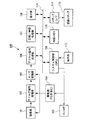
図1は、本発明にかかる実施形態の撮像装置の概略構成を示す図である。なお、本実施形態では、撮像装置の一例としてデジタルカメラの構成を用いて説明する。図1の撮像装置100は、撮像部10と、アナログ信号処理部102と、A/D変換部103と、駆動部104と、ストロボ105と、デジタル信号処理部106と、圧縮/伸張処理部107と、表示部108と、システム制御部109と、内部メモリ110と、メディアインタフェース111と、記録メディア112と、操作部113とを備える。デジタル信号処理部106、圧縮/伸張処理部107、表示部108、システム制御部109、内部メモリ110、及びメディアインタフェース111は、システムバス114に接続されている。
Hereinafter, embodiments of the present invention will be described in detail with reference to the drawings.
FIG. 1 is a diagram illustrating a schematic configuration of an imaging apparatus according to an embodiment of the present invention. In the present embodiment, a configuration of a digital camera will be described as an example of an imaging apparatus. An
撮像部10は、撮影レンズ等の光学系及び後述する固体撮像素子によって被写体の撮影を行うものであり、アナログの撮像信号を出力する。撮像部10には、固体撮像素子への光の入射の遮断制御を行うメカニカルシャッタも含まれている。アナログ信号処理部102は、撮像部10で得られた撮像信号に所定のアナログ信号処理を施す。A/D変換部103は、アナログ信号処理部102で処理後のアナログ信号をデジタル信号に変換する。A/D変換部103の出力は、いわゆるRAW画像データとしてデジタル信号処理部106に送られる。RAW画像データは、撮像部10からの撮像信号の形式のままデジタル化したデジタル画像データである。
The
撮影に際しては、駆動部104を介して光学系、メカニカルシャッタ、及び固体撮像素子の制御が行われる。固体撮像素子は、操作部113の一部であるレリーズボタン(図示せず)の操作による2段レリーズスイッチ(図示せず)のオンを契機として、所定のタイミングで、駆動部104に含まれるタイミングジェネレータ(図1ではTGと記載)からの駆動信号によって駆動される。駆動部104は、システム制御部109によって所定の駆動信号を出力する。
At the time of shooting, the optical system, mechanical shutter, and solid-state image sensor are controlled via the
デジタル信号処理部106は、A/D変換部3からのデジタル画像データに対して、操作部113によって設定された動作モードに応じたデジタル信号処理を行う。デジタル信号処理部106が行う処理には、黒レベル補正処理(OB処理)、リニアマトリクス補正処理、ホワイトバランス調整処理、ガンマ補正処理、画像合成処理、同時化処理、及びY/C変換処理等が含まれる。デジタル信号処理部106は、例えばDSPで構成される。
The digital
圧縮/伸張処理部107は、デジタル信号処理部106で得られたY/Cデータに対して圧縮処理を施すとともに、記録メディア112から得られた圧縮画像データに対して伸張処理を施す。
The compression /
表示部108は、例えばLCD表示装置を含んで構成され、撮影されてデジタル信号処理を経た画像データに基づく画像を表示する。記録メディア112に記録された圧縮画像データを伸張処理して得た画像データに基づく画像の表示も行う。また、撮影時のスルー画像、デジタルカメラの各種状態、操作に関する情報の表示等も可能である。
The
内部メモリ110は、例えばDRAMであり、デジタル信号処理部106やシステム制御部109のワークメモリとして利用される他、記録メディアに112に記録される撮影画像データを一時的に記憶するバッファメモリや表示部108への表示画像データのバッファメモリとしても利用される。メディアインタフェース111は、メモリカード等の記録メディア112との間のデータの入出力を行うものである。
The
システム制御部109は、所定のプログラムによって動作するプロセッサを主体に構成され、撮影動作を含むデジタルカメラ全体の制御を行う。
The
操作部113は、デジタルカメラ使用時の各種操作を行うものであり、レリーズボタン等を含んでいる。
The
図1に示すデジタルカメラは、撮影感度の設定が変更可能となっている。例えばフィルム感度でいえば、ISO感度100に相当する感度で撮影を行う低感度撮影モードと、ISO感度200、400、800に相当する感度で撮影を行う高感度撮影モードとを切換設定可能となっている。図1に示すデジタルカメラでは、例えば、露光時間等の撮像条件を変えることでISO感度を変えており、ISO感度が低いほど露光時間を長く設定し、ISO感度が高いほど露光時間を短く設定している。
In the digital camera shown in FIG. 1, the setting of the photographing sensitivity can be changed. For example, in terms of film sensitivity, it is possible to switch between a low-sensitivity shooting mode in which shooting is performed at a sensitivity equivalent to
図2は、本実施形態の固体撮像素子の構成を説明する平面模式図である。固体撮像素子は、半導体基板の受光領域上に複数のフォトダイオード等の光電変換部11が二次状に配列されている。本実施形態では、各光電変換素子が画像を構成する一画素に相当し、以下、単に画素、又は、画素部ともいう。
FIG. 2 is a schematic plan view illustrating the configuration of the solid-state imaging device of the present embodiment. In the solid-state imaging device, a plurality of
図2のおいて上下方向を列方向、左右方向を行方向としたとき、光電変換部11が半導体基板表面に行方向及び列方向に配設され、奇数行の光電変換部と偶数行の光電変換部とが1/2ピッチづつずらして配列(所謂、ハニカム画素配列)されている。なお、本実施形態では、光電変換部11は、それぞれ波長選択性の異なる第1の光電変換部11aと第2の光電変換部11bとから構成されている。以下の説明では、第1の光電変換部11aと第2の光電変換部11bとを総称して単に光電変換部11ともいう。波長選択性の異なるとは、波長選択範囲の中心が異なる事、または波長選択範囲の幅が異なる事を意味する。例えば、波長選択範囲自体が異なるもの、波長選択範囲は片方の範囲に含まれるが、波長選択幅が異なることで選択範囲の中心が異なるもの、波長選択範囲は片方の範囲に含まれ選択範囲の中心が同一であるが、波長選択幅が異なるものがあげられる。
In FIG. 2, when the vertical direction is the column direction and the horizontal direction is the row direction, the
固体撮像素子20は、各光電変換部11から読み出された信号電荷を列方向に転送する複数の垂直転送部12と、複数の垂直転送部12のそれぞれからの信号電荷を、行方向に転送する水平転送部13と、水平転送部13を経て信号電荷に対応する電圧信号を出力する出力アンプ部14とが設けられている。
The solid-
垂直転送部12は、列方向に配設された複数の光電変換部11に対応して半導体基板に形成された複数の垂直転送チャネル(図示しない)と、複数の垂直転送チャネルのそれぞれと交差するように形成された(図2において左右方向に延設された)複数の垂直転送電極V1〜V8と、各光電変換部11の信号電荷を垂直転送チャネルに読み出す電荷読み出し領域とを含む。各垂直転送部12の垂直転送電極V1〜V8は、光電変換部11の各列同士の間に延在し、蛇行形状を有している。垂直転送部12は、垂直転送電極V1〜V8に駆動部104から出力される垂直転送パルスによって転送駆動される。
The
水平転送部13は、半導体基板に形成された図示しない水平転送チャネルと、この水平転送チャネル上に設けられた水平転送電極とを有し、水平転送電極に駆動部104から出力される水平転送パルスφH1,φH2によって2相駆動される。
The horizontal transfer unit 13 includes a horizontal transfer channel (not shown) formed on the semiconductor substrate and a horizontal transfer electrode provided on the horizontal transfer channel, and a horizontal transfer pulse output from the
出力アンプ部14は、水平転送部13の転送方向端部まで転送されてきた信号電荷の電荷量に応じた電圧値信号を画像信号として出力する。 The output amplifier unit 14 outputs, as an image signal, a voltage value signal corresponding to the amount of signal charges transferred to the end in the transfer direction of the horizontal transfer unit 13.
なお、垂直転送部12や水平転送部13のように、「垂直」「水平」という語句を用いて説明したが、これは、半導体基板表面に平行な「1方向」「この1方向に対して略直角の方向」の意味である。
The
固体撮像素子において、カラー画像信号を検出するため、受光領域上に図示しない、波長選択フィルタとして機能するカラーフィルタが設けられている。 In the solid-state imaging device, in order to detect a color image signal, a color filter that functions as a wavelength selection filter (not shown) is provided on the light receiving region.
波長選択された電荷は、波長選択フィルタとして機能するカラーフィルタを通過した光が光電変換部で受光されることで生成される。なお、波長選択フィルタが存在しない場合では光電変換部の波長選択性を利用することで実現可能である。光電変換部の波長選択性としては、半導体基板の深さ方向の光電変換特性と波長への感受性は関連があることが知られており、例えば、フォトダイオードを半導体受光面の浅い部分に形成すると青のように波長の短い光を選択することができる。さらに、光電変換部と波長選択フィルタとを組み合わせることで、より自由度の高い波長選択性を実現することも可能である。 The wavelength-selected charge is generated when light that has passed through a color filter that functions as a wavelength selection filter is received by the photoelectric conversion unit. In addition, when there is no wavelength selection filter, it is realizable by utilizing the wavelength selectivity of a photoelectric conversion part. As the wavelength selectivity of the photoelectric conversion unit, it is known that the photoelectric conversion characteristics in the depth direction of the semiconductor substrate and the sensitivity to the wavelength are related, for example, when a photodiode is formed in a shallow part of the semiconductor light receiving surface. Light with a short wavelength such as blue can be selected. Furthermore, it is also possible to realize wavelength selectivity with a higher degree of freedom by combining a photoelectric conversion unit and a wavelength selection filter.
各光電変換部11上に図示した「R」「G」「B」「r」「g」「b」は、各光電変換部上に積層されたカラーフィルタの色を表しており、「R」「r」は赤色を示し、「G」「g」は緑色を示し、「B」「b」は青色を示している。また、「R」「G」「B」で示す位置の光電変換部11bと、「r」「g」「b」で示す位置の光電変換部11aとはそれぞれ波長選択性が異なることを示している。光電変換部11によって検出される光に対応する信号を、各色に対応してR信号、G信号、B信号、(又は、r信号、g信号、b信号)と記述する場合もある。
“R”, “G”, “B”, “r”, “g”, and “b” illustrated on each
本実施形態では、光電変換部11が同一の配列ピッチで格子状に配列され、行方向又は列方向に対して約45度斜めにした配列である。本実施形態では、半導体基板表面に行方向及び列方向に配設され、第1の光電変換部11aと第2の光電変換部11bとが、同一の配列ピッチで、かつ、互いに、配列ピッチの1/2だけ行方向及び列方向にずれた位置に配列されている。具体的には、第1の光電変換部11aと第2の光電変換部11bとがそれぞれ赤色,緑色,青色のベイヤー配列を有し、また、奇数行に「r」「g」「b」で示される第2の光電変換部11aが配列され、偶数行に「R」「G」「B」で示される第1の光電変換部11bが配列されている。ここで、上下に並んだ行の同色に対応する光電変換部(例えば「r」と「R」)同士が行方向及び列方向に1/2ピッチづつずれて配置されている。同じ色に対応する光電変換部11のうち、第1の光電変換部11aと第2の光電変換部11bとが、半導体基板の配列において互いに隣接する位置に配置されている。言い換えると、複数の画素部は、入射光に対してそれぞれ異なる波長選択性を有する。ここで、波長選択性とは、カラーフィルタ等によって各画素部に受光する光の波長が規定される性質を意味する。
In the present embodiment, the
第1の光電変換部11a及び第2の光電変換部11bそれぞれの、入射光に対する受光の感度が異なるように構成してもよい。感度が異なる構成としては、受光領域の面積を光電変換部11ごとに変化させるなどの素子の構成を変えてもよく、または、分光の鋭さを変えてもよい。また、露光時間で感度を変えてもよい。光電変換部11の感度を変化さえる方法は、特に限定されない。光電変換部11によって画素部の波長選択性が規定されてもよい。
The first
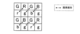
図3及び図4は、本実施形態のカラーフィルタの波長選択性を説明する模式図である。図5は、カラーフィルタの配列の一例を説明する平面模式図である。なお、図5では、「R1」,「R2」が赤色波長の光の波長選択性を有する光電変換部及び画素の位置を示し、「G1」,「G2」が赤色波長の光の波長選択性を有する光電変換部及び画素の位置を示し、「B1」,「B2」が赤色波長の光の波長選択性を有する光電変換部及び画素部の位置を示している。 3 and 4 are schematic diagrams for explaining the wavelength selectivity of the color filter of this embodiment. FIG. 5 is a schematic plan view illustrating an example of the arrangement of color filters. In FIG. 5, “R1” and “R2” indicate the positions of photoelectric conversion units and pixels having wavelength selectivity of red wavelength light, and “G1” and “G2” indicate wavelength selectivity of red wavelength light. And “B1” and “B2” indicate the positions of the photoelectric conversion unit and the pixel unit having wavelength selectivity of red wavelength light.
図3に示すように、「B1」の画素部がBに示す波長選択範囲を有し、「B2」の画素部がbに示す波長選択範囲を有し、「G1」の画素部がGに示す波長選択範囲を有し、「G2」の画素部がgに示す波長選択範囲を有し、「R1」の画素部がRに示す波長選択範囲を有し、「R2」の画素部がrに示す波長選択範囲を有するものとする。「B1」と「B2」との画素部対、「B1」と「B2」との画素部対、「B1」と「B2」との画素部対、はそれぞれ異色画素部対である。異色画素部対とは、同色系の波長選択範囲を有するが、波長選択範囲の中心が異なる画素部対を意味する。波長選択範囲の中心とは、波長選択範囲を波長(nm)で表したときに、その中心となる波長に相当する。 As shown in FIG. 3, the pixel portion “B1” has a wavelength selection range indicated by B, the pixel portion “B2” has a wavelength selection range indicated by b, and the pixel portion “G1” becomes G. The pixel portion “G2” has the wavelength selection range indicated by g, the pixel portion “R1” has the wavelength selection range indicated by R, and the pixel portion “R2” has r The wavelength selection range shown in FIG. The pixel part pair of “B1” and “B2”, the pixel part pair of “B1” and “B2”, and the pixel part pair of “B1” and “B2” are different color pixel pair, respectively. The different color pixel part pair means a pixel part pair having a wavelength selection range of the same color system but having a different center of the wavelength selection range. The center of the wavelength selection range corresponds to the wavelength that is the center when the wavelength selection range is expressed in wavelength (nm).
具体的には、波長選択範囲Bの中心と波長選択範囲bの中心とはずれており、同一ではない。つまり、「B1」と「B2」の画素部対は、それぞれの波長選択範囲の中心が異なり、かつ、それぞれの波長選択範囲を合わせた範囲がB(青色)の波長選択範囲と略同一となる。 Specifically, the center of the wavelength selection range B is not the same as the center of the wavelength selection range b. That is, the pixel unit pairs of “B1” and “B2” are different in the center of each wavelength selection range, and the combined range of the wavelength selection ranges is substantially the same as the wavelength selection range of B (blue). .
波長選択範囲Gの中心と波長選択範囲gの中心とはずれており、同一ではない。つまり、「G1」と「G2」の画素部対は、それぞれの波長選択範囲の中心が異なり、かつ、それぞれの波長選択範囲を合わせた範囲がG(緑色)の波長選択範囲と略同一となる。 The center of the wavelength selection range G is not the same as the center of the wavelength selection range g. In other words, the pixel unit pairs “G1” and “G2” are different in the center of each wavelength selection range, and the combined range of the wavelength selection ranges is substantially the same as the wavelength selection range of G (green). .
波長選択範囲Rの中心と波長選択範囲rの中心とはずれており、同一ではない。つまり、「R1」と「R2」の画素部対は、それぞれの波長選択範囲の中心が異なり、かつ、それぞれの波長選択範囲を合わせた範囲がR(赤色)の波長選択範囲と略同一となる。 The center of the wavelength selection range R is not the same as the center of the wavelength selection range r. That is, the pixel unit pairs of “R1” and “R2” are different in the center of each wavelength selection range, and the combined range of each wavelength selection range is substantially the same as the wavelength selection range of R (red). .
図4に示すように、本実施形態の固体撮像素子は、第1の光電変換部11aと第2の光電変換部11bとで生成されたそれぞれの信号電荷を加算することで、RGBを近似している。第1の光電変換部11aと第2の光電変換部11bとの上に設けられたカラーフィルタの波長選択性が異なっており、第1の光電変換部11aで生成された赤色信号R1と第2の光電変換部11bで生成された赤色信号R2とを2画素加算することでR信号を検出し、第1の光電変換部11aで生成された緑色信号G1と第2の光電変換部11bで生成された緑色信号G2とを2画素加算することでG信号を検出し、第1の光電変換部11aで生成された青色信号B1と第2の光電変換部11bで生成された青色信号B2とを2画素加算することでB信号を検出する。ここで、本実施形態では、2画素を加算し、RGBのそれぞれを近似したが、3画素以上の光電変換部11で生成された信号電荷を加算してもよい。また、本実施形態では、RGBのすべてを近似により検出したが、これに限定されず、RGBのうち、いずれか1色又は2色のみを近似により検出することができる。例えば、G信号のみを近似により検出し、R及びB信号については、単一の光電変換部で生成された信号電荷に基いて検出することができる。
As shown in FIG. 4, the solid-state imaging device of this embodiment approximates RGB by adding the respective signal charges generated by the first
図5に示すように、本実施形態の固体撮像素子においては、加算される画素同士のフィルタが隣接するように配列されている。具体的には、加算されることでR信号を近似する、R1信号を生成する画素とR2信号を生成する画素とが、両者の間に他の画素が配置されることなく、互いに半導体基板の行方向及び列方向に対して1/2ピッチずれた位置に並べて設けられている。同様に、加算されることでG信号を近似する、G1信号を生成する画素とG2信号を生成する画素とが、両者の間に他の画素が配置されることなく、互いに半導体基板の行方向及び列方向に対して1/2ピッチずれた位置に並べて設けられている。加算されることでB信号を近似する、B1信号を生成する画素とB2信号を生成する画素とが、両者の間に他の画素が配置されることなく、互いに半導体基板の行方向及び列方向に対して1/2ピッチずれた位置に並べて設けられている。 As shown in FIG. 5, in the solid-state imaging device of the present embodiment, the filters of pixels to be added are arranged so as to be adjacent to each other. Specifically, the pixel that generates the R1 signal and the pixel that generates the R2 signal, which approximate the R signal by being added, are arranged on the semiconductor substrate without any other pixel being placed between them. They are arranged side by side at a position shifted by 1/2 pitch with respect to the row direction and the column direction. Similarly, the pixel that generates the G1 signal and the pixel that generates the G2 signal, which approximate the G signal by addition, are arranged in the row direction of the semiconductor substrate without any other pixel being disposed between them. And arranged side by side at a position shifted by 1/2 pitch with respect to the column direction. The pixel that generates the B1 signal and the pixel that generates the B2 signal, which approximate the B signal by addition, are mutually arranged in the row direction and the column direction of the semiconductor substrate without any other pixel being disposed between them. Are arranged side by side at positions shifted by 1/2 pitch.
本実施形態では、R1とR2、G1とG2、B1とB2のそれぞれの加算される画素の配列が同じ方向となっていることが好ましい。こうすることで、画素加算による画質の低下をより一層抑制することができる。また、本実施形態の画素配列では、隣接する2画素を加算した場合に、加算された画素の配列がベイヤー配列となることが好ましい。 In the present embodiment, it is preferable that the arrangement of the added pixels of R1 and R2, G1 and G2, and B1 and B2 is in the same direction. By doing so, it is possible to further suppress the deterioration in image quality due to pixel addition. In the pixel array of the present embodiment, when two adjacent pixels are added, the added pixel array is preferably a Bayer array.
図2及び図5に示すように、画素の配列がハニカム構造の場合には、全画素読み出しが可能であるため、途中読み出した第1の光電変換部又は第2の光電変換部で生成された信号電荷のみ独立に読み出すことができる。さらに、光電変換部が2行ごとに、読み出す方向が異なる構造とすることで、第1の光電変換部及び第2の光電変換部のうち一方で生成された信号電荷のみ独立に転送することができる。これにより、転送可能な信号電荷量を増やすことができるため、ダイナミックレンジを更に拡大することができる。 As shown in FIG. 2 and FIG. 5, when the pixel arrangement has a honeycomb structure, all pixels can be read out, so that the pixel is generated by the first photoelectric conversion unit or the second photoelectric conversion unit read out in the middle. Only the signal charge can be read out independently. Furthermore, the photoelectric conversion unit has a structure in which the reading direction is different every two rows, so that only the signal charges generated by one of the first photoelectric conversion unit and the second photoelectric conversion unit can be transferred independently. it can. As a result, the amount of signal charge that can be transferred can be increased, so that the dynamic range can be further expanded.
本発明は、画素の信号電荷を加算することでRGBのうち少なくとも1色を近似可能な波長選択性を有している。例えば、それぞれ波長選択範囲の中心が異なる第1の緑フィルタと第2の緑フィルタとを設け、それぞれの画素で生成された信号電荷を画素加算することで、一つのG(緑色)信号とすることができる。また、それぞれ波長選択範囲の中心が異なる第1の赤フィルタと第2の赤フィルタとを設け、それぞれの画素で生成された信号電荷を画素加算することで、一つのR(赤色)信号とすることができ、または、それぞれ波長選択範囲の中心が異なる第1の青フィルタと第2の青フィルタとを設け、それぞれの画素で生成された信号電荷を画素加算することで、一つのB(青色)信号とすることができる。こうすれば、隣接画素の相関性の高さにより原色の精度が向上する。また、隣接する画素同士を加算することで、アーティファクトが発生し難く、画像の高画質化を図ることができる。 The present invention has wavelength selectivity capable of approximating at least one color of RGB by adding pixel signal charges. For example, a first green filter and a second green filter, each having a different wavelength selection range, are provided, and the signal charges generated in the respective pixels are added to form a single G (green) signal. be able to. Also, a first red filter and a second red filter, each having a different wavelength selection range, are provided, and the signal charges generated in the respective pixels are added to form a single R (red) signal. Or by providing a first blue filter and a second blue filter, each having a different center of wavelength selection range, and adding the signal charges generated in the respective pixels to one B (blue ) Signal. In this way, the accuracy of the primary color is improved due to the high correlation between adjacent pixels. In addition, by adding adjacent pixels together, artifacts hardly occur and the image quality can be improved.
本発明にかかる撮像装置は、加算される画素(または、異色画素部対を構成する画素)の感度の比を制御する感度比制御手段を有していてもよい。加算される画素の感度比の制御は、例えば、画素の構成を変えてもよく、分光の鋭さ(Q)を変えることで実現が可能である。こうすることで、異色画素部対に含まれる画素部の感度がそれぞれ異なるように構成可能である。さらに露光時間を変えてもよい。また、感度をかえる画素の組は、加算される画素の画素同士の位置関係と同様に、同一の位置関係であることが好ましい。 The imaging apparatus according to the present invention may include a sensitivity ratio control unit that controls a ratio of sensitivity of pixels to be added (or pixels constituting a different color pixel unit pair). The control of the sensitivity ratio of the added pixels may be realized, for example, by changing the configuration of the pixels or by changing the sharpness (Q) of the spectrum. By doing so, it is possible to configure the pixel units included in the different color pixel unit pairs to have different sensitivities. Further, the exposure time may be changed. Moreover, it is preferable that the set of pixels whose sensitivity is changed has the same positional relationship as the positional relationship between the pixels of the added pixels.
次に、本発明にかかる撮像装置の他の構成例を図面に基いて説明する。なお、以下に説明する実施形態において、すでに説明した部材などと同等な構成・作用を有する部材等については、図中に同一符号又は相当符号を付すことにより、説明を簡略化或いは省略する。 Next, another configuration example of the imaging apparatus according to the present invention will be described with reference to the drawings. In the embodiments described below, members having the same configuration / action as those already described are denoted by the same or corresponding reference numerals in the drawings, and description thereof is simplified or omitted.
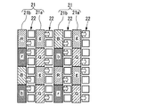
図6及び図7に示す固体撮像素子では、各光電変換部21が、半導体基板上において行方向及び列方向に同一の配列ピッチで格子状に配列されている。具体的には、光電変換部21a,21bが半導体基板表面に行方向及び列方向に配設され、第1の光電変換部21aと第2の光電変換部21bとが、同一の配列ピッチで、かつ、それぞれが正方格子状に2×2周期の配列を斜めにした状態で配列されている。光電変換部21a及び光電変換部21bは、それぞれ、ベイヤー配列を略45度傾けた状態で格子状に配置されている。
In the solid-state imaging device shown in FIGS. 6 and 7, the
図6に示す固体撮像素子では、第1の光電変換部21a及び第2の光電変換部21bにおいて検出された画素信号が、ともに同じ垂直転送部22に読み出される。転送時には、R信号,G信号,B信号は、列方向に延在する複数の垂直転送電極のうち、列方向にn番目,n+4番目,n+8番目・・・(n=1,2,3…などの任意の整数とする。)に読み出され、r信号,g信号,b信号は、列方向に延在する複数の垂直転送電極のうち、列方向にn+1番目,n+5番目,n+9番目・・・に読み出される。図6に示す光電変換部の配列によれば、垂直転送電極に駆動パルスを印加することによって読み出された各信号電荷を4相駆動で垂直転送できる。
In the solid-state imaging device shown in FIG. 6, pixel signals detected by the first
また、図6の光電変換部21の配列によれば、光電変換部21のうち、互いに加算される画素に対応する、第1の光電変換部21aと第2の光電変換部21bとが、列方向に隣り合う位置に配置されている。
Further, according to the arrangement of the
図7の固体撮像素子では、第1の光電変換部21a及び第2の光電変換部21bにおいて検出された画素信号が、それぞれ反対側の垂直転送部22に読み出される。図7では、第2の光電変換部21bで検出された画素信号が図中右側の垂直転送部22に読み出され、第1の光電変換部21aで検出された画素信号が図中左側の垂直転送部22に読み出される。転送時には、R,G,B信号は、列方向に延在する複数の垂直転送電極のうち、列方向にn番目,n+4番目,n+8番目・・・に読み出され、r,g,b信号は、反対側に延在する複数の垂直転送電極のうち、列方向にn+1番目,n+5番目,n+9番目・・・に読み出される。図7に示す光電変換部の配列によれば、垂直転送電極に駆動パルスを印加することによって信号電荷を4相駆動で垂直転送できる。
In the solid-state imaging device of FIG. 7, pixel signals detected by the first
また、図7の光電変換部21の配列によれば、同じ色に対応する光電変換部21のうち、第1の光電変換部21aと第2の光電変換部21bとが、垂直転送部22を挟んで行方向に隣り合う位置に配置されている。
Further, according to the arrangement of the
図6及び図7に示す固体撮像素子のカラーフィルタの構成においても、RGBの各色のいずれかに近似される色に対する分光波長領域が拡大するため、色再現性を向上することができる。また、隣接する画素同士を加算することで、アーティファクトが発生し難く、画像の高画質化を図ることができる。
また、図6及び図7に示す固体撮像素子は、隣接する2画素を加算した場合に、加算された画素の配列がベイヤー配列となることが好ましい。
Also in the configuration of the color filter of the solid-state imaging device shown in FIGS. 6 and 7, since the spectral wavelength region for a color approximated to any of the RGB colors is expanded, color reproducibility can be improved. In addition, by adding adjacent pixels together, artifacts hardly occur and the image quality can be improved.
Further, in the solid-state imaging device shown in FIGS. 6 and 7, when two adjacent pixels are added, it is preferable that the added pixel arrangement becomes a Bayer arrangement.
上記のカラーフィルタは、RGBのそれぞれが、波長選択性の異なる2つの画素を加算によって近似される6色のマルチバンドものとしたが、カラーフィルタはこれに限定されない。例えば、4色、5色、または、7色以上の色フィルタを備えたマルチバンド構成とすることができる。 In the above color filter, each of RGB is a multi-band of 6 colors approximated by adding two pixels having different wavelength selectivity, but the color filter is not limited to this. For example, a multiband configuration including color filters of four colors, five colors, or seven colors or more can be employed.
図8は、4色の色フィルタを有するカラーフィルタの配列例のを示す図である。なお、図8では、2画素×2画素に対応するフィルタ配列のみを示しているが、行方向及び列方向に繰り返す所定の配列パターンであるとする。
図8(a)に示すフィルタ配列においては、R画素とr画素上に、それぞれ波長選択性が異なるフィルタが配置されている。そして、R画素及びr画素で生成された信号電荷を加算することで、赤色信号を近似している。一方、G画素及びB画素上には、それぞれ単一の色フィルタ配列され、それぞれG信号とB信号が読み出される。こうすれば、赤色の波長領域に対する分解能を向上させることができる。
FIG. 8 is a diagram showing an example of an arrangement of color filters having four color filters. In FIG. 8, only the filter array corresponding to 2 pixels × 2 pixels is shown, but it is assumed that the predetermined array pattern repeats in the row direction and the column direction.
In the filter array shown in FIG. 8A, filters having different wavelength selectivity are arranged on the R pixel and the r pixel, respectively. Then, the red signal is approximated by adding the signal charges generated by the R pixel and the r pixel. On the other hand, a single color filter is arranged on each of the G pixel and the B pixel, and the G signal and the B signal are read out, respectively. In this way, the resolution for the red wavelength region can be improved.
図8(b)に示すフィルタ配列においては、B画素とb画素上に、それぞれ波長選択性が異なるフィルタが配置されている。そして、B画素及びb画素で生成された信号電荷を加算することで、青色信号を近似している。一方、R画素及びG画素上には、それぞれ単一の色フィルタ配列され、それぞれR信号とG信号が読み出される。こうすれば、青色の波長領域に対する分解能を向上させることができる。 In the filter array shown in FIG. 8B, filters having different wavelength selectivity are arranged on the B pixel and the b pixel, respectively. And the blue signal is approximated by adding the signal charge produced | generated by B pixel and b pixel. On the other hand, a single color filter is arranged on each of the R pixel and the G pixel, and the R signal and the G signal are read out, respectively. In this way, the resolution for the blue wavelength region can be improved.
図8(c)に示すフィルタ配列においては、G画素とg画素上に、それぞれ波長選択性が異なるフィルタが配置されている。そして、G画素及びg画素で生成された信号電荷を加算することで、緑色信号を近似している。一方、R画素及びB画素上には、それぞれ単一の色フィルタ配列され、それぞれR信号とB信号が読み出される。こうすれば、緑色の波長領域に対する分解能を向上させることができる。また、図5の色ペアでR1とR2、B1とB2を同じ波長選択性としてもよい。同じ特性としてはそれぞれR、Bとすることが望ましい。これにより緑の波長領域に対する分解能を向上させることができる。R、Bの場合も同様である。 In the filter array shown in FIG. 8C, filters having different wavelength selectivity are arranged on the G pixel and the g pixel, respectively. And the green signal is approximated by adding the signal charge produced | generated by G pixel and g pixel. On the other hand, a single color filter is arranged on each of the R pixel and the B pixel, and the R signal and the B signal are read out, respectively. In this way, the resolution for the green wavelength region can be improved. Further, R1 and R2, and B1 and B2 may be the same wavelength selectivity in the color pair of FIG. It is desirable that R and B are the same characteristics. Thereby, the resolution for the green wavelength region can be improved. The same applies to R and B.
図9は、本実施形態のカラーフィルタの他の構成例を説明する模式図である。図10は、カラーフィルタの配列を説明する平面模式図である。なお、図10では、「R1」,「R2」が赤色波長の光の波長選択範囲を有する光電変換部及び画素の位置を示し、「G1」,「G2」が緑色波長の光の波長選択範囲を有する光電変換部及び画素の位置を示し、「B1」,「B2」が青色波長の光の波長選択範囲を有する光電変換部及び画素の位置を示している。 FIG. 9 is a schematic diagram illustrating another configuration example of the color filter of the present embodiment. FIG. 10 is a schematic plan view for explaining the arrangement of the color filters. In FIG. 10, “R1” and “R2” indicate the positions of the photoelectric conversion unit and the pixel having the wavelength selection range of the red wavelength light, and “G1” and “G2” indicate the wavelength selection range of the green wavelength light. And “B1” and “B2” indicate the positions of the photoelectric conversion unit and the pixel having the wavelength selection range of the blue wavelength light.
本発明において、カラーフィルタが画素の信号電荷を加算もしくは参照することでRGBのうち少なくとも1色を近似可能な波長選択性を有する構成に加え、更に、隣接画素を参照することでRGBの補色のうち少なくとも1色を近似可能な波長選択性を有する構成とすることができる。 In the present invention, the color filter adds or refers to the signal charge of the pixel and has a wavelength selectivity that can approximate at least one color of RGB, and further, by referring to an adjacent pixel, the complementary color of RGB can be obtained. It can be set as the structure which has the wavelength selectivity which can approximate at least 1 color among them.
図9に示すように、第1の光電変換部で生成された青色信号B1と第2の光電変換部で生成された赤色信号R2とを参照することでマゼンタ信号Mgを検出できる。また、第2の光電変換部で生成された青色信号B2と第1の光電変換部で生成された緑色信号G1とを参照することでシアン信号Cyを検出できる。さらに、第2の光電変換部で生成された緑色信号G2と第1の光電変換部で生成された赤色信号R1とを参照することでイエロー信号Yeを検出できる。 As shown in FIG. 9, the magenta signal Mg can be detected by referring to the blue signal B1 generated by the first photoelectric conversion unit and the red signal R2 generated by the second photoelectric conversion unit. Further, the cyan signal Cy can be detected by referring to the blue signal B2 generated by the second photoelectric conversion unit and the green signal G1 generated by the first photoelectric conversion unit. Further, the yellow signal Ye can be detected by referring to the green signal G2 generated by the second photoelectric conversion unit and the red signal R1 generated by the first photoelectric conversion unit.
このとき、図10に示すように、参照することで補色に近似される2画素(ここでは、B2画素とG1画素、G2画素とR1画素、B1画素とR2画素)がいずれもフィルタ配列において隣接するように配置されている。こうすれば、固体撮像素子の駆動時に、独立に読み出しを行うことでRGBの色情報に加えて、補色の色情報を精度良く得ることができるため色再現性を更に向上させることができる。また、5色の場合も、Rが単色の場合はB2とG1、Bが単色の場合はG2とR1、Gが単色の場合はR2とB1で補色に近似できる。このように、異色画素部対に含まれる画素部と、該画素部隣接する画素部との組み合わせでそれぞれの波長選択範囲の和が、補色の少なくとも1つに対応する波長選択範囲と略同一となるように画素部を配列してもよい。 At this time, as shown in FIG. 10, two pixels approximated to complementary colors by reference (here, B2 pixel and G1 pixel, G2 pixel and R1 pixel, B1 pixel and R2 pixel) are adjacent in the filter array. Are arranged to be. In this case, when the solid-state imaging device is driven, the color reproducibility can be further improved because the complementary color information can be obtained with high accuracy in addition to the RGB color information by performing independent reading. In the case of five colors, B2 and G1 can be approximated to complementary colors when R is a single color, G2 and R1 when B is a single color, and R2 and B1 when G is a single color. As described above, the sum of the wavelength selection ranges in the combination of the pixel portion included in the different color pixel portion pair and the pixel portion adjacent to the pixel portion is substantially the same as the wavelength selection range corresponding to at least one of the complementary colors. The pixel portions may be arranged so that
撮像素子の構成としては、CMOS型の構成とすることができる。図11は、CMOS型の回路構成を説明する模式図である。図12は、図11の撮像素子のカラーフィルタの配列の一例を示す平面模式図である。配列は、RGB及びrgbの6色のカラーフィルタ配列である。また、この配列では、R画素部とr画素部とが異色画素部対を構成し、G画素部とg画素部とが異色画素部対を構成し、これら2組の異色画素部対によって2×2の画素部を構成する。 The configuration of the imaging element can be a CMOS configuration. FIG. 11 is a schematic diagram illustrating a CMOS type circuit configuration. 12 is a schematic plan view showing an example of the arrangement of color filters of the image sensor shown in FIG. The array is a color filter array of six colors of RGB and rgb. In this arrangement, the R pixel portion and the r pixel portion constitute a different color pixel portion pair, and the G pixel portion and the g pixel portion constitute a different color pixel portion pair. A x2 pixel portion is formed.
図11に示すCMOS型の撮像素子は、上記2×2の画素部に対応する回路構成を備えている。具体的には、各画素部は、半導体基板に形成されたフォトダイオードPDと、PDで生成された電荷を転送するための転送トランジスタTrを備えている。画素部のうち異色画素部対を構成する画素部同士が、PDの電荷を互いに加算可能となるように接続されている。また、2組の異色画素部対が互いに接続され、単一のフローティングディフュージョンFDに接続されている。FDには、FDの電位を電源電圧VDDにリセットするためのリセットトランジスタRSTが接続されている。また、FDには、増幅トランジスタTaのゲートが接続されている。この増幅トランジスタTaは、選択トランジスタTsを介して、垂直出力線に接続されている。画素選択信号に基づいて選択トランジスタTsがオンすると、増幅トランジスタTaはFDの電位を増幅してその電位に応じた電圧を垂直信号線に出力する。
この構成によれば、2×2の画素部に対応し、4画素部の信号電荷を加算して読み出すことが可能な構成である。
The CMOS type image sensor shown in FIG. 11 has a circuit configuration corresponding to the 2 × 2 pixel portion. Specifically, each pixel unit includes a photodiode PD formed on a semiconductor substrate and a transfer transistor Tr for transferring charges generated by the PD. Among the pixel portions, the pixel portions constituting the different color pixel portion pair are connected so that the charges of the PD can be added to each other. Also, two pairs of different color pixel portions are connected to each other and connected to a single floating diffusion FD. A reset transistor RST for resetting the potential of the FD to the power supply voltage VDD is connected to the FD. Further, the gate of the amplification transistor Ta is connected to the FD. The amplification transistor Ta is connected to the vertical output line through the selection transistor Ts. When the selection transistor Ts is turned on based on the pixel selection signal, the amplification transistor Ta amplifies the potential of the FD and outputs a voltage corresponding to the potential to the vertical signal line.
According to this configuration, it corresponds to a 2 × 2 pixel portion, and can be read by adding the signal charges of the four pixel portions.
次に、CCD構造の撮像素子において、6色のカラーフィルタ配列として垂直転送部で画素加算する例を説明する。
図13は、図6及び図7の構成の変形例である。図14は、図13の撮像素子のカラーフィルタの配列の一例を示す平面模式図である。この配列では、R画素部とr画素部とが異色画素部対を構成し、G画素部とg画素部とが異色画素部対を構成する。
Next, an example in which pixels are added by a vertical transfer unit as a color filter array of six colors in an image pickup device having a CCD structure will be described.
FIG. 13 is a modification of the configuration of FIGS. FIG. 14 is a schematic plan view showing an example of the arrangement of the color filters of the image sensor shown in FIG. In this arrangement, the R pixel portion and the r pixel portion constitute a different color pixel portion pair, and the G pixel portion and the g pixel portion constitute a different color pixel portion pair.
図13の光電変換部21の配列によれば、光電変換部21のうち、互いに加算される画素部に対応する、第1の光電変換部21aと第2の光電変換部21bとが、同一の垂直転送部22を挟んでその両側に位置し、それぞれの画素信号の読み出し方向が向かい合うように配置されている。例えば、異色画素部対を構成するR画素部とr画素部は、両画素部の間に位置する垂直転送部22に画素信号が読み出される。
According to the arrangement of the
図7の固体撮像素子では、第1の光電変換部21a及び第2の光電変換部21bにおいて検出された画素信号が、それぞれ反対側の垂直転送部22に読み出される。図7では、第2の光電変換部21bで検出された画素信号が図中右側の垂直転送部22に読み出され、第1の光電変換部21aで検出された画素信号が図中左側の垂直転送部22に読み出される。そして、異色画素部対を構成する画素部同士の画素信号が垂直転送部22で加算される。
In the solid-state imaging device of FIG. 7, pixel signals detected by the first
カラーフィルタの配列は適宜変更可能である。
図15は、RGBとrbの画素部によって構成された5色の配列である。ここで、R画素部とr画素部とが異色画素部対を構成し、また、B画素部とb画素部とが異色画素部対を構成する。ここで、G画素部とG画素部とは、波長選択範囲の中心が同一である同色画素部対を構成する。このように画素部対は、異色画素部対のみの配列に限定されず、異色画素部対と同色画素部対とから構成されていてもよい。
The arrangement of the color filters can be changed as appropriate.
FIG. 15 shows an array of five colors constituted by RGB and rb pixel portions. Here, the R pixel portion and the r pixel portion constitute a different color pixel portion pair, and the B pixel portion and the b pixel portion constitute a different color pixel portion pair. Here, the G pixel portion and the G pixel portion constitute a pair of the same color pixels where the centers of the wavelength selection ranges are the same. Thus, the pixel part pair is not limited to the arrangement of only the different color pixel part pair, and may be composed of the different color pixel part pair and the same color pixel part pair.
図16は、RGBとrgbの画素部によって構成された6色の配列である。この配列では、R画素部とr画素部とが異色画素部対を構成し、B画素部とb画素部とが異色画素部対を構成し、G画素部とg画素部とが異色画素部対を構成する。また、これら異色画素部対のうち2組の異色画素部対によって2×2画素部が構成される。また、この配列では、2ラインごとに2×2画素部の配置が、1画素分だけラインの方向にずれている。こうすれば、2組の異色画素部対の画素信号を加算したときに、加算後の重心が市松状になり、ライン方向の解像度(例えば画像中の縦線に対する解像度)を向上することができる利点がある。 FIG. 16 shows an array of six colors constituted by RGB and rgb pixel portions. In this arrangement, the R pixel portion and the r pixel portion constitute a different color pixel portion pair, the B pixel portion and the b pixel portion constitute a different color pixel portion pair, and the G pixel portion and the g pixel portion constitute a different color pixel portion. Configure a pair. In addition, a 2 × 2 pixel portion is constituted by two pairs of different color pixel portions among these different color pixel portion pairs. Further, in this arrangement, the arrangement of 2 × 2 pixel portions is shifted in the line direction by one pixel every two lines. In this way, when the pixel signals of the two pairs of different color pixel parts are added, the center of gravity after the addition becomes a checkered pattern, and the resolution in the line direction (for example, the resolution for the vertical line in the image) can be improved. There are advantages.
このように、撮像素子には、入射光に対して異なる波長選択性を有する画素部が少なくとも4種類備えられていればよい。例えば、RGBとrの画素部の4種類とすれば、R画素部とr画素部とで少なくとも1つの異色画素部対を構成することができる。このとき、B画素部同士及びG画素部同士で、それぞれ同色画素部対を構成してもよい。 As described above, the imaging element only needs to include at least four types of pixel portions having different wavelength selectivity with respect to incident light. For example, if there are four types of RGB and r pixel units, the R pixel unit and the r pixel unit can form at least one different color pixel unit pair. At this time, the same color pixel unit pair may be formed by the B pixel units and the G pixel units.
10 撮像部
11a,21a 第1の光電変換部
11b,21b 第2の光電変換部
12 垂直転送部
13 水平転送部
20 固体撮像素子
100 撮像装置
DESCRIPTION OF
Claims (28)
複数の前記画素部が、隣接する2種類の画素部からなる画素部対を含み、前記画素部対は異なる波長選択性を持ち、かつ、それぞれの波長選択範囲を合わせた範囲が3原色のうち1つの波長選択範囲と略同一となる異色画素部対を少なくとも1つ含み、前記画素部対ごとに加算された画素の配列がベイヤー配列となる撮像素子。 An imaging device comprising at least four types of pixel portions having different wavelength selectivity with respect to incident light,
The plurality of pixel units include a pixel unit pair composed of two types of adjacent pixel units, the pixel unit pair has different wavelength selectivity, and a range obtained by combining the wavelength selection ranges is out of three primary colors one of the at least one saw including a wavelength selection substantially the same become different color pixel portion pair, the imaging device array of pixels summed for each of the pixel portion pair is the Bayer arrangement.
複数の前記画素部が、隣接する2種類の画素部からなる画素部対を含み、前記画素部対は異なる波長選択性を持ち、かつ、それぞれの波長選択範囲を合わせた範囲が3原色のうち1つの波長選択範囲と略同一となる異色画素部対を少なくとも1つ含み、前記異色画素部対が3種類であり、該異色画素部対の波長選択範囲の和がそれぞれ3原色に対応し、全体として6種類の波長選択範囲を有する画素部を備える撮像素子。 An imaging device comprising at least four types of pixel portions having different wavelength selectivity with respect to incident light,
The plurality of pixel units include a pixel unit pair composed of two types of adjacent pixel units, the pixel unit pair has different wavelength selectivity, and a range obtained by combining the wavelength selection ranges is out of three primary colors Including at least one different color pixel portion pair substantially the same as one wavelength selection range, the different color pixel portion pairs are three types, and the sum of the wavelength selection ranges of the different color pixel portion pairs respectively corresponds to the three primary colors; An imaging device including a pixel portion having six types of wavelength selection ranges as a whole .
複数の前記画素部が、隣接する2種類の画素部からなる画素部対を含み、前記画素部対は異なる波長選択性を持ち、かつ、それぞれの波長選択範囲を合わせた範囲が3原色のうち1つの波長選択範囲と略同一となる異色画素部対を少なくとも1つ含み、前記画素部対ごとに加算された画素の配列がベイヤー配列となる撮像装置。 An imaging apparatus including an imaging device including at least four types of pixel units having different wavelength selectivity with respect to incident light,
The plurality of pixel units include a pixel unit pair composed of two types of adjacent pixel units, the pixel unit pair has different wavelength selectivity, and a range obtained by combining the wavelength selection ranges is out of three primary colors at least one viewing contains one wavelength selection substantially the same become different color pixel portion pair, the imaging device array of pixels summed for each of the pixel portion pair is the Bayer arrangement.
複数の前記画素部が、隣接する2種類の画素部からなる画素部対を含み、前記画素部対は異なる波長選択性を持ち、かつ、それぞれの波長選択範囲を合わせた範囲が3原色のうち1つの波長選択範囲と略同一となる異色画素部対を少なくとも1つ含み、前記異色画素部対が3種類であり、該異色画素部対の波長選択範囲の和がそれぞれ3原色に対応し、全体として6種類の波長選択範囲を有する画素部を備える撮像装置。 An imaging apparatus including an imaging device including at least four types of pixel units having different wavelength selectivity with respect to incident light,
The plurality of pixel units include a pixel unit pair composed of two types of adjacent pixel units, the pixel unit pair has different wavelength selectivity, and a range obtained by combining the wavelength selection ranges is out of three primary colors at least one viewing contains one wavelength selection substantially the same become different color pixel portion pair, the different color pixel portion pairs is three, the sum of the wavelength selection range of the different color pixel unit pair corresponding to each of the three primary colors An imaging apparatus including a pixel unit having six types of wavelength selection ranges as a whole .
Priority Applications (1)
| Application Number | Priority Date | Filing Date | Title |
|---|---|---|---|
| JP2009067933A JP4448889B2 (en) | 2008-04-01 | 2009-03-19 | Imaging device and imaging apparatus |
Applications Claiming Priority (2)
| Application Number | Priority Date | Filing Date | Title |
|---|---|---|---|
| JP2008095398 | 2008-04-01 | ||
| JP2009067933A JP4448889B2 (en) | 2008-04-01 | 2009-03-19 | Imaging device and imaging apparatus |
Publications (2)
| Publication Number | Publication Date |
|---|---|
| JP2009268078A JP2009268078A (en) | 2009-11-12 |
| JP4448889B2 true JP4448889B2 (en) | 2010-04-14 |
Family
ID=41393278
Family Applications (1)
| Application Number | Title | Priority Date | Filing Date |
|---|---|---|---|
| JP2009067933A Expired - Fee Related JP4448889B2 (en) | 2008-04-01 | 2009-03-19 | Imaging device and imaging apparatus |
Country Status (1)
| Country | Link |
|---|---|
| JP (1) | JP4448889B2 (en) |
Families Citing this family (11)
| Publication number | Priority date | Publication date | Assignee | Title |
|---|---|---|---|---|
| JP5253295B2 (en) * | 2009-05-20 | 2013-07-31 | キヤノン株式会社 | Image input device, image processing method, and computer program |
| JP5146499B2 (en) * | 2009-08-08 | 2013-02-20 | 株式会社ニコン | Solid-state image sensor |
| JP5422362B2 (en) * | 2009-12-15 | 2014-02-19 | 株式会社東芝 | Solid-state imaging device |
| JP5627252B2 (en) * | 2010-03-01 | 2014-11-19 | キヤノン株式会社 | Imaging apparatus and control method thereof |
| WO2011132617A1 (en) * | 2010-04-20 | 2011-10-27 | 富士フイルム株式会社 | Imaging device and method of driving solid-state image sensor |
| CN103004211B (en) * | 2010-04-20 | 2015-09-02 | 富士胶片株式会社 | The method of imaging device and process photographic images |
| WO2011132619A1 (en) * | 2010-04-20 | 2011-10-27 | 富士フイルム株式会社 | Solid state imaging element and imaging device |
| WO2011148799A1 (en) * | 2010-05-28 | 2011-12-01 | 富士フイルム株式会社 | Imaging device and method of calculating white balance gain |
| CN102948152B (en) * | 2010-06-22 | 2015-09-16 | 富士胶片株式会社 | Imaging device and formation method |
| JP5629568B2 (en) * | 2010-12-16 | 2014-11-19 | 富士フイルム株式会社 | Imaging device and pixel addition method thereof |
| WO2013100037A1 (en) * | 2011-12-27 | 2013-07-04 | 富士フイルム株式会社 | Color imaging element |
-
2009
- 2009-03-19 JP JP2009067933A patent/JP4448889B2/en not_active Expired - Fee Related
Also Published As
| Publication number | Publication date |
|---|---|
| JP2009268078A (en) | 2009-11-12 |
Similar Documents
| Publication | Publication Date | Title |
|---|---|---|
| JP4448889B2 (en) | Imaging device and imaging apparatus | |
| JP4484944B2 (en) | Imaging device and driving method of imaging device | |
| JP4448888B2 (en) | Imaging apparatus and signal processing method of imaging apparatus | |
| US7944496B2 (en) | Imaging apparatus and driving method for CCD type solid-state imaging device | |
| US8077232B2 (en) | Imaging device for adding signals including same color component | |
| JP4951440B2 (en) | Imaging apparatus and solid-state imaging device driving method | |
| JP5501448B2 (en) | Imaging apparatus and solid-state imaging device driving method | |
| JP4291793B2 (en) | Solid-state imaging device and solid-state imaging device | |
| JP5150796B2 (en) | Solid-state imaging device driving method, solid-state imaging device, and imaging apparatus | |
| JP3970185B2 (en) | Solid-state image sensor and digital camera | |
| JP2008104013A (en) | Driving method of solid-state imaging element and imaging apparatus | |
| JP2006270364A (en) | Solid-state image pickup element and solid-state image pickup device, and driving method thereof | |
| JP2009065478A (en) | Driving method of solid-state image sensor, and imaging apparatus | |
| JP2008278453A (en) | Image sensing apparatus and image capturing system | |
| JP5033711B2 (en) | Imaging device and driving method of imaging device | |
| JP2009117979A (en) | Method of driving solid-state imaging device | |
| JP4393242B2 (en) | Solid-state imaging device and driving method of solid-state imaging device | |
| JP2009055321A (en) | Imaging device and method of driving ccd solid image sensor | |
| JP5124549B2 (en) | Moving image signal readout method and imaging apparatus for solid-state imaging device | |
| JP2007235877A (en) | Multi-ccd solid-state imaging element module and imaging apparatus | |
| JP2007235888A (en) | Single-ccd color solid-state imaging element and imaging apparatus | |
| JP2007088732A (en) | Solid-state imaging element | |
| JP2005259750A (en) | Multiple-disk color solid state imaging device and digital camera | |
| JP4848349B2 (en) | Imaging apparatus and solid-state imaging device driving method | |
| JP5256084B2 (en) | Imaging device and driving method of imaging device |
Legal Events
| Date | Code | Title | Description |
|---|---|---|---|
| A621 | Written request for application examination |
Free format text: JAPANESE INTERMEDIATE CODE: A621 Effective date: 20090925 |
|
| A871 | Explanation of circumstances concerning accelerated examination |
Free format text: JAPANESE INTERMEDIATE CODE: A871 Effective date: 20090925 |
|
| A975 | Report on accelerated examination |
Free format text: JAPANESE INTERMEDIATE CODE: A971005 Effective date: 20091021 |
|
| A131 | Notification of reasons for refusal |
Free format text: JAPANESE INTERMEDIATE CODE: A131 Effective date: 20091111 |
|
| A521 | Request for written amendment filed |
Free format text: JAPANESE INTERMEDIATE CODE: A523 Effective date: 20091124 |
|
| TRDD | Decision of grant or rejection written | ||
| A01 | Written decision to grant a patent or to grant a registration (utility model) |
Free format text: JAPANESE INTERMEDIATE CODE: A01 Effective date: 20100106 |
|
| A01 | Written decision to grant a patent or to grant a registration (utility model) |
Free format text: JAPANESE INTERMEDIATE CODE: A01 |
|
| A61 | First payment of annual fees (during grant procedure) |
Free format text: JAPANESE INTERMEDIATE CODE: A61 Effective date: 20100125 |
|
| FPAY | Renewal fee payment (event date is renewal date of database) |
Free format text: PAYMENT UNTIL: 20130129 Year of fee payment: 3 |
|
| R150 | Certificate of patent or registration of utility model |
Ref document number: 4448889 Country of ref document: JP Free format text: JAPANESE INTERMEDIATE CODE: R150 Free format text: JAPANESE INTERMEDIATE CODE: R150 |
|
| FPAY | Renewal fee payment (event date is renewal date of database) |
Free format text: PAYMENT UNTIL: 20130129 Year of fee payment: 3 |
|
| FPAY | Renewal fee payment (event date is renewal date of database) |
Free format text: PAYMENT UNTIL: 20140129 Year of fee payment: 4 |
|
| R250 | Receipt of annual fees |
Free format text: JAPANESE INTERMEDIATE CODE: R250 |
|
| R250 | Receipt of annual fees |
Free format text: JAPANESE INTERMEDIATE CODE: R250 |
|
| R250 | Receipt of annual fees |
Free format text: JAPANESE INTERMEDIATE CODE: R250 |
|
| R250 | Receipt of annual fees |
Free format text: JAPANESE INTERMEDIATE CODE: R250 |
|
| R250 | Receipt of annual fees |
Free format text: JAPANESE INTERMEDIATE CODE: R250 |
|
| R250 | Receipt of annual fees |
Free format text: JAPANESE INTERMEDIATE CODE: R250 |
|
| R250 | Receipt of annual fees |
Free format text: JAPANESE INTERMEDIATE CODE: R250 |
|
| R250 | Receipt of annual fees |
Free format text: JAPANESE INTERMEDIATE CODE: R250 |
|
| R250 | Receipt of annual fees |
Free format text: JAPANESE INTERMEDIATE CODE: R250 |
|
| LAPS | Cancellation because of no payment of annual fees |