US8077232B2 - Imaging device for adding signals including same color component - Google Patents
Imaging device for adding signals including same color component Download PDFInfo
- Publication number
- US8077232B2 US8077232B2 US12/625,254 US62525409A US8077232B2 US 8077232 B2 US8077232 B2 US 8077232B2 US 62525409 A US62525409 A US 62525409A US 8077232 B2 US8077232 B2 US 8077232B2
- Authority
- US
- United States
- Prior art keywords
- pixels
- pixel
- signals
- added
- imaging device
- Prior art date
- Legal status (The legal status is an assumption and is not a legal conclusion. Google has not performed a legal analysis and makes no representation as to the accuracy of the status listed.)
- Expired - Fee Related
Links
Images


Classifications
-
- H—ELECTRICITY
- H04—ELECTRIC COMMUNICATION TECHNIQUE
- H04N—PICTORIAL COMMUNICATION, e.g. TELEVISION
- H04N25/00—Circuitry of solid-state image sensors [SSIS]; Control thereof
- H04N25/40—Extracting pixel data from image sensors by controlling scanning circuits, e.g. by modifying the number of pixels sampled or to be sampled
- H04N25/46—Extracting pixel data from image sensors by controlling scanning circuits, e.g. by modifying the number of pixels sampled or to be sampled by combining or binning pixels
-
- H—ELECTRICITY
- H04—ELECTRIC COMMUNICATION TECHNIQUE
- H04N—PICTORIAL COMMUNICATION, e.g. TELEVISION
- H04N23/00—Cameras or camera modules comprising electronic image sensors; Control thereof
- H04N23/10—Cameras or camera modules comprising electronic image sensors; Control thereof for generating image signals from different wavelengths
- H04N23/12—Cameras or camera modules comprising electronic image sensors; Control thereof for generating image signals from different wavelengths with one sensor only
-
- H—ELECTRICITY
- H04—ELECTRIC COMMUNICATION TECHNIQUE
- H04N—PICTORIAL COMMUNICATION, e.g. TELEVISION
- H04N23/00—Cameras or camera modules comprising electronic image sensors; Control thereof
- H04N23/80—Camera processing pipelines; Components thereof
- H04N23/84—Camera processing pipelines; Components thereof for processing colour signals
-
- H—ELECTRICITY
- H04—ELECTRIC COMMUNICATION TECHNIQUE
- H04N—PICTORIAL COMMUNICATION, e.g. TELEVISION
- H04N25/00—Circuitry of solid-state image sensors [SSIS]; Control thereof
- H04N25/10—Circuitry of solid-state image sensors [SSIS]; Control thereof for transforming different wavelengths into image signals
- H04N25/11—Arrangement of colour filter arrays [CFA]; Filter mosaics
- H04N25/13—Arrangement of colour filter arrays [CFA]; Filter mosaics characterised by the spectral characteristics of the filter elements
- H04N25/134—Arrangement of colour filter arrays [CFA]; Filter mosaics characterised by the spectral characteristics of the filter elements based on three different wavelength filter elements
Definitions
- the present invention relates to an imaging device for taking images of a subject.
- imaging elements having up to ten million pixels have been employed for digital still cameras of which primary usage is taking still images, and also imaging elements having several million pixels have been employed for movie cameras of which primary usage is taking moving images.
- taking images has been performed with the high number of pixels in the event of taking high-definition images required for high resolution, and with the low number of pixels in the event of low resolution.
- an imaging device comprises a plurality of photoelectric converting units arrayed in the vertical and horizontal directions, and adding means for adding the signals including the same color component provided from the plurality of photoelectric converting units such that the centers of gravity of the signals after addition are at the same pitch for respective signals.
- This configuration realizes all-pixel readout in the event of taking high-definition images, high sensitivity, high-speed readout, and high quality in the event of taking low-resolution images.
- FIG. 1 is a diagram illustrating an example of array of respective colors before adding pixel signals.
- FIGS. 2A through 2E are explanatory diagrams illustrating color array after adding pixel signals and signals to be added for each color.
- FIG. 3 is a block diagram of an imaging element making up an imaging device.
- FIG. 4 is a partial circuit diagram of a signal processing circuit of pixel signals read out from an imaging region.
- FIG. 5 is an explanatory diagram wherein a signal in increments of a plurality of lines to be added is read out.
- FIG. 6 is an explanatory diagram wherein a signal following addition within a screen is read out.
- FIG. 7 is an explanatory diagram in a case of employing a mechanical shutter.
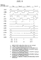
- FIG. 8 is a timing chart of readout of pixel signals and addition thereof.
- FIG. 9 is a system diagram.
- FIG. 10 is a unit pixel circuit diagram of a pixel unit.
- FIG. 11 is an example of a pixel configuration diagram of a common amplifier pixel.
- FIG. 1 is a diagram illustrating an example of array of respective colors before adding pixel signals
- FIGS. 2A through 2E are diagrams illustrating color array after adding pixel signals and signals to be added for each color.
- color filters G Green), R (Red), and B (Blue) are configured on each photodiode of an imaging element.
- G is arrayed in a checkerboard pattern, and R and B are arrayed every other line, in other words, 2 ⁇ 2, i.e., 4 pixels of R, G, G, and B are disposed two-dimensionally as one unit pixel color matrix.
- FIG. 2A shows addition of Rij signals, i.e., signals on the Rn, Rn+2, and Rn+4 columns corresponding to the m, m+2, and m+4 lines are added.
- FIG. 2C is a diagram illustrating addition of Gi and j+1 signals, FIG.
- FIG. 2D is a diagram illustrating addition of Gi+1, j signals
- FIG. 2E is a diagram illustrating addition of Bi+1 and j+1 signals.
- each color is added while overlapping spatially, thus, the center of gravity of spatial sampling is at the same pitch for respective color signals following addition, and further, all of the pixel signals are used. Accordingly, moire on the image due to offset of spatial sampling is removed, and also sensitivity (in particular, optical shot noise) improves by ⁇ 9, i.e., triple the conventional sensitivity.
- the present invention is applied to an imaging element having five million pixels, the number of pixels after addition becomes the number of pixels equivalent to around VGA, and accordingly, readout of high-speed shooting with high sensitivity can be realized.
- the number of addition pixels may be increased to 5 ⁇ 5 or 7 ⁇ 7. This yields the advantage of increased sensitivity. Even if the number of addition pixels increases, all that is necessary is to increase the memory CA of a later-described adder circuit by the number of lines to be added.
- FIG. 3 is a block diagram of an imaging element of an imaging device according to the present embodiment of the invention.
- a pixel unit made up of a photodiode for performing photoelectric conversion such as shown in FIG. 10 described later, a pixel amplifier, and the like, are disposed and connected to an imaging region, in matrix fashion.
- the pixel unit of this imaging region is controlled by a plurality of driving pulses from a vertical scanning circuit (V. SR) 10 .
- V. SR vertical scanning circuit
- the odd numbered vertical signal lines of the imaging region are connected to a CDS/amplifier-circuit/memory-circuit 20 - 1
- the even numbered vertical signal lines are connected to a CDS/amplifier-circuit/memory-circuit 20 - 2 .
- the circuit blocks above and below the imaging region have the same configuration in the drawing, so hereinafter, description will be made regarding only the circuit block below the imaging region. With the signal from the pixel unit, noise of the pixel unit is removed at the CDS/amplifier-circuit/memory-circuit 20 - 1 , and only the signal components are amplified and stored to the memory 1 .
- the signals in the memory 1 are controlled by scanning pulses ⁇ hn ( 1 ), ⁇ hn ( 2 ), and ⁇ hn ( 3 ) from horizontal scanning circuits (H. SR), and are read out to an output signal line.
- the signals in the memory 1 are led to adder circuits 30 - 1 .
- the signals having the same color from the memory 1 are added.
- the signals subjected to addition are temporarily accumulated in memory 2 , and are controlled by the scanning pulse ⁇ hn (a) from the horizontal scanning circuits (H. SR), and then are read out to the output signal line.
- FIG. 10 illustrates a unit pixel circuit diagram of the pixel unit
- FIG. 4 is a partial circuit diagram of a readout signal processing circuit of pixel signals from the imaging region
- FIG. 8 illustrates a timing chart of addition of pixel signals. While description will be made regarding readout from the pixel unit and addition of signals with reference to these drawings, the arrangement in FIG. 4 illustrates an example of addition of 3 ⁇ 3 pixels within the imaging block diagram in FIG. 3 .
- the pixel unit in FIG. 10 is made up of a photodiode PD serving as a photoelectric converting unit, a transfer switch MTX for controlling transfer of signal charge from the photodiode PD, a pixel amplifier MSF connected to the transfer switch MTX, a reset switch MRES for resetting the residual charge of a gate portion (floating diffusion) of the pixel amplifier MSF, and a selection switch MSEL for controlling transfer of signals from the pixel amplifier.
- a current source switch MRV of the pixel amplifier is provided on the outside of the imaging region.
- a circuit made up of a capacitance C, a clamp switch MC, a reference voltage source VR, and an amplifier Amp is a CDS circuit for removing noise from the pixel unit.
- Circuits for temporarily accumulating signals of 3 columns subjected to CDS are memory capacitances CT 1 , CT 2 , and CT 3 of the memory 1 circuit.
- a circuit for adding and temporarily accumulating three signals of the memory 1 circuit is a memory capacitance CA 1 .
- circuits for temporarily accumulating different signals to be added on the horizontal pixel lines are memory capacitances CA 2 and CA 3 .
- a circuit for adding and temporarily accumulating the signals from these memory capacitances CA 1 , CA 2 , and CA 3 is a capacitance CT 2 of the memory 2 circuits.
- each residual charge at the node of each circuit unit is reset under control of each pulse.
- the gate portion of the pixel amplifier MSF is reset with a pulse ⁇ RES, the memory 1 circuit by pulses ⁇ C 1 and ⁇ S 1 , the adder unit capacitances CA 1 , CA 2 , and CA 3 by pulses ⁇ AD 4 , ⁇ C 2 , and ⁇ AD 5 , respectively.
- pixel amplifier noise is clamped by the clamp capacitance C when the pulse ⁇ C 1 is off, and the charge of the photodiode is input to the clamp capacitance C by a pulse ⁇ TX via the pixel amplifier.
- the pixel noise is removed by CDS, and temporarily accumulated in the memory 1 circuit via the amplifier Amp.
- the signals from the vertical signal lines V 1 , V 3 , and V 5 i.e., signals Rm and n are temporarily accumulated in the memory capacitance CT 1
- the signal Rm and a signal n+2 are accumulated in the memory capacitance CT 2
- the signal Rm and a signal n+4 are accumulated in the memory capacitance CT 3 respectively.
- the transfer of the photoelectric conversion signal of the row m pixel is completed with a pulse ⁇ SEL and the pulse ⁇ TS 1 turning off.
- a signal from the memory 1 circuit is added to the adder memory capacitance CA 1 with pulses ⁇ TS 2 and ⁇ AD 1 .
- the row m+2 pixel signal is added and temporarily accumulated in the memory capacitance CA 2 at time t 5
- the row m+4 pixel signal is added and temporarily accumulated in the memory capacitance CA 3 at time t 6 .
- the signals of the memory capacitances CA 1 , CA 2 , and CA 3 are added in a memory capacitance CT 2 n with the pulses ⁇ AD 4 and ⁇ AD 5 . Consequently, nine pixels worth of an R signal is added in the memory capacitance CT 2 n, thereby obtaining signals Ri and j to be added.
- the memory 2 circuit may be equivalent to the number of addition pixels, for example, the number equivalent to VGA. This depends on the concept of the imaging system. An arrangement may be made wherein the pixel signals of the whole screen are transferred at high speed, and are added and temporarily accumulated in the memory 2 circuit in arbitrary increments, and then the pixel signals are read out sequentially. As shown in FIG. 4 , the present embodiment handles both the all-pixel readout mode and the addition-readout mode with the memory 1 circuit. In particular, addition is performed with the memory 1 circuit regardless of addition of a great number of a plurality of pixels of 3 ⁇ 3 i.e., 9 pixels, thereby reducing memory in size. This is effective in reducing the imaging element in size.
- the present invention sets the amplifier gain of the amplifier circuit following CDS at the addition-readout mode to around triple that of the all-pixel readout mode. Consequently, the noise of the output amplifier can be reduced, thereby achieving improvement of sensitivity owing to addition of pixel signals, high-speed readout by reducing the number of pixels to be read out, maintenance of a high dynamic range, and low consumption of electricity.
- FIG. 5 is an example of readout of signals in increments of a plurality of lines to be added.
- a signal is read out from a pixel in increments of lines to be added, and is added to the signals in the memory, following which the signal is output externally from the memory during one horizontal scan.
- all pixels of the imaging region are reset in block, following exposure, and following addition of all pixel signals on the whole screen in arbitrary increments, addition pixels equivalent to VGA are temporarily accumulated in the plurality of memory 2 circuits, and then the signal is output from the memory 2 circuits sequentially.
- FIG. 6 all pixels of the imaging region are reset in block, following exposure, and following addition of all pixel signals on the whole screen in arbitrary increments, addition pixels equivalent to VGA are temporarily accumulated in the plurality of memory 2 circuits, and then the signal is output from the memory 2 circuits sequentially.
- FIG. 7 illustrates a case of employing a mechanical shutter wherein all the pixels of the imaging region are reset in block, following exposure with the mechanical shutter, and following addition of pixel signals in arbitrary increments, the pixel signals are output externally from the memory 2 circuit during one horizontal scan.
- FIG. 11 is a common amplifier configuration. This is an example of the configuration wherein two photodiodes correspond to one pixel amplifier. In the event that a plurality of photodiodes are disposed as to one amplifier, the area of the pixel amplifier as to one photodiode is reduced, resulting in an advantage wherein the opening percentage of the photodiode improves.
- FIG. 9 illustrates a schematic diagram of the system with the above-described imaging element.
- a subject light entering through an optical system 71 forms an image on a sensor 72 .
- the light information is converted into electric signals by pixels disposed on the sensor.
- the electric signals are subjected to signal conversion processing with a predetermined method determined by a signal processing circuit 73 beforehand.
- the signals subjected to the signal processing are recorded or transmitted with a recording-system/communicating-system 74 , and with an information-recording device.
- the signals recorded or transferred are reproduced or displayed with a reproducing-system/display-system 77 .
- the sensor 72 and the signal processing circuit 73 are controlled by a timing control circuit 75 , and the timing control circuit 75 , the recording-system/communicating-system 74 , and the reproducing-system/display-system 77 , are controlled by a system control circuit 76 .
- the timing control circuit 75 selects the all-pixel readout mode or the addition-readout mode.
- Horizontal and vertical driving pulses are different between the all-pixel readout mode and the addition-readout mode. Accordingly, there is the need to change the driving timing of the sensor, resolution processing of the signal processing circuit, the number of recording pixels of the recording system for each readout mode.
- the above-described control is performed by the system control circuit depending on each readout mode. Sensitivity due to addition differs depending on the readout mode. With regard to this difference in sensitivity, the system control circuit controls the diaphragm (not shown), and the timing control circuit switches the gain of the amplifier circuit Amp of the sensor so as to be increased with a control pulse from the timing control circuit, thereby obtaining an appropriate signal.
Landscapes
- Engineering & Computer Science (AREA)
- Multimedia (AREA)
- Signal Processing (AREA)
- Physics & Mathematics (AREA)
- Spectroscopy & Molecular Physics (AREA)
- Transforming Light Signals Into Electric Signals (AREA)
- Color Television Image Signal Generators (AREA)
- Solid State Image Pick-Up Elements (AREA)
Abstract
An imaging device includes a plurality of photoelectric converting units arrayed in the horizontal and vertical directions, and an adder for adding signals including the same color component from the a plurality of photoelectric converting units such that the centers of gravity of the signals after addition are at the same pitch for respective signals.
Description
This application is a continuation of U.S. patent application Ser. No. 10/936,904 filed Sep. 9, 2004, which claims priority from Japanese Patent Application No. 2003-318388 filed Sep. 10, 2003, all of which are hereby incorporated by reference herein in their entirety.
1. Field of the Invention
The present invention relates to an imaging device for taking images of a subject.
2. Description of the Related Art
In recent years, imaging elements having up to ten million pixels have been employed for digital still cameras of which primary usage is taking still images, and also imaging elements having several million pixels have been employed for movie cameras of which primary usage is taking moving images. With the above-described usages, in general, taking images has been performed with the high number of pixels in the event of taking high-definition images required for high resolution, and with the low number of pixels in the event of low resolution. In this process, in the event of taking high-definition images, generally all pixel signals have been read out from the imaging elements, and in the event of taking low-resolution images, pixel-signal thinning-out readout and readout for performing both pixel-signal thinning-out and addition, have been performed either to prevent the camera from excessive battery consumption, or to increase the number of shots. Examples of the above-described conventional arrangements include Japanese Patent Laid-Open No. 9-247689 and Japanese Patent Laid-Open No. 2001-36920.
With the arrangement disclosed in Japanese Patent Laid-Open No. 9-247689 (FIG. 3 in the Publication), readout addition is performed by thinning out the same color in increments of 4×4 pixels.
With the arrangement disclosed in Japanese Patent Laid-Open No. 2001-36920 (FIG. 1 in the Publication), a plurality of pixel signals are added, with 4×4 pixels making up one group, such that spatial color array of each color is the same before and after addition.
With Japanese Patent Laid-Open No. 9-247689, the number of valid pixels used in 4×4 pixels is few. Recent imaging elements have reduced unit-pixel size owing to high pixelation, and insufficient sensitivity is becoming a more prominent issue. With digital still cameras, while insufficient sensitivity in shooting of a dark subject can be compensated for with flash emission, taking moving images generates a great amount of noise since an expensive and heavy light source cannot be used. Furthermore, moiré occurs due to deterioration of image sampling frequency owing to pixel-signal thinning-out, resulting in marked deterioration of image quality.
With Japanese Patent Laid-Open No. 9-247689, while sensitivity can be improved by increasing the number of pixel signals to be added within one group, a problem is to provide pixel signals, which are not used (discarded). Moreover, while a plurality of pixel signals are added within one group such that spatial color array of each color becomes the same before and after addition, a problem is that a small amount of moiré can be observed under magnification.
As described above, with the conventional techniques, there are problems wherein improvement of sensitivity is insufficient due to thinning out of pixel signals, and also, moiré occurs even though the spatial color array is the same.
It is an object of the present invention to provide good image quality even in the event of obtaining a low-resolution image by adding a plurality of pixel signals.
In order to achieve the above-described object, according to a first aspect of the present invention, an imaging device comprises a plurality of photoelectric converting units arrayed in the vertical and horizontal directions, and adding means for adding the signals including the same color component provided from the plurality of photoelectric converting units such that the centers of gravity of the signals after addition are at the same pitch for respective signals.
This configuration realizes all-pixel readout in the event of taking high-definition images, high sensitivity, high-speed readout, and high quality in the event of taking low-resolution images.
Other objects and features of the present invention will become apparent from the following description of the preferred embodiments with reference to the attached drawings.
Embodiments of the present invention will now be described in detail in accordance with the accompanying drawings.
With an example of color array in FIG. 1 , let us say that color filters G (Green), R (Red), and B (Blue) are configured on each photodiode of an imaging element. In this example, G is arrayed in a checkerboard pattern, and R and B are arrayed every other line, in other words, 2×2, i.e., 4 pixels of R, G, G, and B are disposed two-dimensionally as one unit pixel color matrix.
With an addition-readout shooting mode of pixel signals according to the present embodiment of the invention, pixel signals are added within an imaging element so as to configure the same color array as shown in FIG. 2A , the result is stored in memory, and then the result is read out from the imaging element. With the embodiment here, an example of addition of 3×3 i.e., 9 pixels of the same color is shown. FIG. 2B shows addition of Rij signals, i.e., signals on the Rn, Rn+2, and Rn+4 columns corresponding to the m, m+2, and m+4 lines are added. In the same way, FIG. 2C is a diagram illustrating addition of Gi and j+1 signals, FIG. 2D is a diagram illustrating addition of Gi+1, j signals, and FIG. 2E is a diagram illustrating addition of Bi+1 and j+1 signals. In this case, each color is added while overlapping spatially, thus, the center of gravity of spatial sampling is at the same pitch for respective color signals following addition, and further, all of the pixel signals are used. Accordingly, moire on the image due to offset of spatial sampling is removed, and also sensitivity (in particular, optical shot noise) improves by √9, i.e., triple the conventional sensitivity. For example, in the event that the present invention is applied to an imaging element having five million pixels, the number of pixels after addition becomes the number of pixels equivalent to around VGA, and accordingly, readout of high-speed shooting with high sensitivity can be realized. Furthermore, in the event that low resolution is necessary, the number of addition pixels may be increased to 5×5 or 7×7. This yields the advantage of increased sensitivity. Even if the number of addition pixels increases, all that is necessary is to increase the memory CA of a later-described adder circuit by the number of lines to be added.
Next, description will be made regarding an example of the internal configuration of an imaging element. FIG. 3 is a block diagram of an imaging element of an imaging device according to the present embodiment of the invention. In the drawing, a pixel unit made up of a photodiode for performing photoelectric conversion such as shown in FIG. 10 described later, a pixel amplifier, and the like, are disposed and connected to an imaging region, in matrix fashion. The pixel unit of this imaging region is controlled by a plurality of driving pulses from a vertical scanning circuit (V. SR) 10. The odd numbered vertical signal lines of the imaging region are connected to a CDS/amplifier-circuit/memory-circuit 20-1, the even numbered vertical signal lines are connected to a CDS/amplifier-circuit/memory-circuit 20-2. The circuit blocks above and below the imaging region have the same configuration in the drawing, so hereinafter, description will be made regarding only the circuit block below the imaging region. With the signal from the pixel unit, noise of the pixel unit is removed at the CDS/amplifier-circuit/memory-circuit 20-1, and only the signal components are amplified and stored to the memory 1. In the event that the present imaging device operates in the all-pixel readout mode rather than in the addition-readout mode, the signals in the memory 1 are controlled by scanning pulses φhn (1), φhn (2), and φhn (3) from horizontal scanning circuits (H. SR), and are read out to an output signal line. In the event of the addition-readout mode, the signals in the memory 1 are led to adder circuits 30-1. At the adder circuits 30-1, the signals having the same color from the memory 1 are added. The signals subjected to addition are temporarily accumulated in memory 2, and are controlled by the scanning pulse φhn (a) from the horizontal scanning circuits (H. SR), and then are read out to the output signal line.
The pixel unit in FIG. 10 is made up of a photodiode PD serving as a photoelectric converting unit, a transfer switch MTX for controlling transfer of signal charge from the photodiode PD, a pixel amplifier MSF connected to the transfer switch MTX, a reset switch MRES for resetting the residual charge of a gate portion (floating diffusion) of the pixel amplifier MSF, and a selection switch MSEL for controlling transfer of signals from the pixel amplifier. A current source switch MRV of the pixel amplifier is provided on the outside of the imaging region.
Description will be made regarding the readout signal processing circuit in FIG. 4 . A circuit made up of a capacitance C, a clamp switch MC, a reference voltage source VR, and an amplifier Amp is a CDS circuit for removing noise from the pixel unit. Circuits for temporarily accumulating signals of 3 columns subjected to CDS are memory capacitances CT1, CT2, and CT3 of the memory 1 circuit. A circuit for adding and temporarily accumulating three signals of the memory 1 circuit is a memory capacitance CA1. In the same way, circuits for temporarily accumulating different signals to be added on the horizontal pixel lines are memory capacitances CA2 and CA3. A circuit for adding and temporarily accumulating the signals from these memory capacitances CA1, CA2, and CA3 is a capacitance CT2 of the memory 2 circuits.
Next, description will be made with reference to the timing chart in FIG. 8 . Upon an arbitrary exposure period elapsing, first, each residual charge at the node of each circuit unit is reset under control of each pulse. At time t1, the gate portion of the pixel amplifier MSF is reset with a pulse φRES, the memory 1 circuit by pulses φC1 and φS1, the adder unit capacitances CA1, CA2, and CA3 by pulses φAD4, φC2, and φAD5, respectively. At time t2, pixel amplifier noise is clamped by the clamp capacitance C when the pulse φC1 is off, and the charge of the photodiode is input to the clamp capacitance C by a pulse φTX via the pixel amplifier.
Consequently, the pixel noise is removed by CDS, and temporarily accumulated in the memory 1 circuit via the amplifier Amp. Now, let us say that vertical scan is performed on the row m in FIG. 1 , the signals from the vertical signal lines V1, V3, and V5, i.e., signals Rm and n are temporarily accumulated in the memory capacitance CT1, the signal Rm and a signal n+2 are accumulated in the memory capacitance CT2, and the signal Rm and a signal n+4 are accumulated in the memory capacitance CT3 respectively.
At time t3, the transfer of the photoelectric conversion signal of the row m pixel is completed with a pulse φSEL and the pulse φTS1 turning off. At time t4, a signal from the memory 1 circuit is added to the adder memory capacitance CA1 with pulses φTS2 and φAD1.
In the same scan and operation, the row m+2 pixel signal is added and temporarily accumulated in the memory capacitance CA2 at time t5, and the row m+4 pixel signal is added and temporarily accumulated in the memory capacitance CA3 at time t6. At time t7, the signals of the memory capacitances CA1, CA2, and CA3 are added in a memory capacitance CT2n with the pulses φAD4 and φAD5. Consequently, nine pixels worth of an R signal is added in the memory capacitance CT2n, thereby obtaining signals Ri and j to be added.
In the same operation, nine pixels worth of a G signal is added in the memory capacitance CT2n+ 1, thereby obtaining signals Gi+1 and j to be added. While this embodiment provides two pixels worth of memory capacitances in the vertical direction, the memory 2 circuit may be equivalent to the number of addition pixels, for example, the number equivalent to VGA. This depends on the concept of the imaging system. An arrangement may be made wherein the pixel signals of the whole screen are transferred at high speed, and are added and temporarily accumulated in the memory 2 circuit in arbitrary increments, and then the pixel signals are read out sequentially. As shown in FIG. 4 , the present embodiment handles both the all-pixel readout mode and the addition-readout mode with the memory 1 circuit. In particular, addition is performed with the memory 1 circuit regardless of addition of a great number of a plurality of pixels of 3×3 i.e., 9 pixels, thereby reducing memory in size. This is effective in reducing the imaging element in size.
With the above-described nine-pixel addition-readout mode, improvement of sensitivity is tripled (as to optical shot noise), and accordingly the system performs amount-of-exposure control, and sets the amount of incident light to around one third. This means that the photoelectric conversion signal at each photodiode is reduced to one third. In the event that the imaging element is a CCD, even if the amount of incident light is one third, the signal charge is tripled following addition by adding nine pixel charge. Accordingly, if nothing is done, saturation of signals becomes a problem. One setback is that sensitivity and saturation properties are mutually counteractive issues.
With a CMOS sensor according to the present embodiment, addition of average values of signal voltage is employed, and accordingly in the event that deterioration of the signal level due to capacitance division is ignored, the signal level is around one third after addition of nine pixel signals. This means that saturation of the signals is enhanced threefold the previous saturation. However, a small signal level means that the noise of the output amplifier connected to the horizontal output line (omitted in FIG. 4 ) is of major concern. Accordingly, the present invention sets the amplifier gain of the amplifier circuit following CDS at the addition-readout mode to around triple that of the all-pixel readout mode. Consequently, the noise of the output amplifier can be reduced, thereby achieving improvement of sensitivity owing to addition of pixel signals, high-speed readout by reducing the number of pixels to be read out, maintenance of a high dynamic range, and low consumption of electricity.
Description will be made regarding arrangements of a method for reading out signals at the addition-readout mode with reference to FIGS. 5 , 6, and 7.
As for the pixel unit of the imaging region, while description has been made regarding a configuration wherein one pixel amplifier corresponds to one photodiode in FIG. 10 , another configuration example of the pixel unit is shown in FIG. 11 , which is a common amplifier configuration. This is an example of the configuration wherein two photodiodes correspond to one pixel amplifier. In the event that a plurality of photodiodes are disposed as to one amplifier, the area of the pixel amplifier as to one photodiode is reduced, resulting in an advantage wherein the opening percentage of the photodiode improves.
Horizontal and vertical driving pulses are different between the all-pixel readout mode and the addition-readout mode. Accordingly, there is the need to change the driving timing of the sensor, resolution processing of the signal processing circuit, the number of recording pixels of the recording system for each readout mode. The above-described control is performed by the system control circuit depending on each readout mode. Sensitivity due to addition differs depending on the readout mode. With regard to this difference in sensitivity, the system control circuit controls the diaphragm (not shown), and the timing control circuit switches the gain of the amplifier circuit Amp of the sensor so as to be increased with a control pulse from the timing control circuit, thereby obtaining an appropriate signal.
While the present invention has been described with reference to what are presently considered to be the preferred embodiments, it is to be understood that the invention is not limited to the disclosed embodiments. On the contrary, the invention is intended to cover various modifications and equivalent arrangements included within the spirit and scope of the appended claims. The scope of the following claims is to be accorded the broadest interpretation so as to encompass all such modifications and equivalent structures and functions.
Claims (3)
1. An imaging device comprising:
a plurality of pixels arrayed in the horizontal and vertical directions, each of the plurality of pixels having a photoelectric converting unit and a pixel amplification unit outputting a signal based on an electrical charge accumulated in the photoelectric converting unit;
a noise removing unit removing noise generated in the pixel; and
a plurality of color filters arranged in a Bayer pattern,
wherein the pixel array has a plurality of regions each comprising adjacent pixels of five rows by five columns, and a center pixel of one region comprising the pixels of five rows by five columns is adjacent to a center pixel of another region comprising the pixels of five rows by five columns with being two pixels spaced apart from the center pixel of the another region in directions of the rows and the columns, and
wherein the imaging device has an addition mode in which signals from plural pixels in a first, third, and fifth rows and a first, third, and fifth columns in each of the regions comprising the pixels of five rows by five columns are added.
2. The imaging device according to claim 1 , further comprising a plurality of column amplification units provided corresponding to the plurality of pixel columns.
3. The imaging device according to claim 1 , wherein the imaging device is operable in a mode in which the signals from the plurality of pixels are added and in a mode in which the signals from the plurality of pixels are not added, and
wherein gain of the column amplification unit in the mode in which the signals are added is higher than the gain of the column amplification unit in the mode in which the signals from the plurality of pixels are not added.
Priority Applications (1)
| Application Number | Priority Date | Filing Date | Title |
|---|---|---|---|
| US12/625,254 US8077232B2 (en) | 2003-09-10 | 2009-11-24 | Imaging device for adding signals including same color component |
Applications Claiming Priority (4)
| Application Number | Priority Date | Filing Date | Title |
|---|---|---|---|
| JP2003-318388 | 2003-09-10 | ||
| JP2003318388A JP4497872B2 (en) | 2003-09-10 | 2003-09-10 | Imaging device |
| US10/936,904 US7646413B2 (en) | 2003-09-10 | 2004-09-09 | Imaging device for adding signals including same color component |
| US12/625,254 US8077232B2 (en) | 2003-09-10 | 2009-11-24 | Imaging device for adding signals including same color component |
Related Parent Applications (1)
| Application Number | Title | Priority Date | Filing Date |
|---|---|---|---|
| US10/936,904 Continuation US7646413B2 (en) | 2003-09-10 | 2004-09-09 | Imaging device for adding signals including same color component |
Publications (2)
| Publication Number | Publication Date |
|---|---|
| US20100066875A1 US20100066875A1 (en) | 2010-03-18 |
| US8077232B2 true US8077232B2 (en) | 2011-12-13 |
Family
ID=34225321
Family Applications (2)
| Application Number | Title | Priority Date | Filing Date |
|---|---|---|---|
| US10/936,904 Expired - Fee Related US7646413B2 (en) | 2003-09-10 | 2004-09-09 | Imaging device for adding signals including same color component |
| US12/625,254 Expired - Fee Related US8077232B2 (en) | 2003-09-10 | 2009-11-24 | Imaging device for adding signals including same color component |
Family Applications Before (1)
| Application Number | Title | Priority Date | Filing Date |
|---|---|---|---|
| US10/936,904 Expired - Fee Related US7646413B2 (en) | 2003-09-10 | 2004-09-09 | Imaging device for adding signals including same color component |
Country Status (4)
| Country | Link |
|---|---|
| US (2) | US7646413B2 (en) |
| JP (1) | JP4497872B2 (en) |
| KR (1) | KR100633506B1 (en) |
| CN (2) | CN1946136B (en) |
Cited By (3)
| Publication number | Priority date | Publication date | Assignee | Title |
|---|---|---|---|---|
| US20080278591A1 (en) * | 2007-05-09 | 2008-11-13 | Barna Sandor L | Method and apparatus for improving low-light performance for small pixel image sensors |
| US20130010153A1 (en) * | 2011-02-24 | 2013-01-10 | Sony Corporation | Image pickup apparatus and image pickup apparatus control method, and program |
| US20180278858A1 (en) * | 2015-02-12 | 2018-09-27 | Sony Corporation | Imaging device and control method thereof, and electronic apparatus |
Families Citing this family (24)
| Publication number | Priority date | Publication date | Assignee | Title |
|---|---|---|---|---|
| JP4290066B2 (en) * | 2004-05-20 | 2009-07-01 | キヤノン株式会社 | Solid-state imaging device and imaging system |
| JP4290071B2 (en) * | 2004-06-02 | 2009-07-01 | キヤノン株式会社 | Solid-state imaging device and imaging system |
| US20060119724A1 (en) * | 2004-12-02 | 2006-06-08 | Fuji Photo Film Co., Ltd. | Imaging device, signal processing method on solid-state imaging element, digital camera and controlling method therefor and color image data generating method |
| JP4497022B2 (en) * | 2005-04-26 | 2010-07-07 | ソニー株式会社 | Solid-state imaging device, driving method of solid-state imaging device, and imaging device |
| JP2007129581A (en) * | 2005-11-04 | 2007-05-24 | Canon Inc | Imaging apparatus and imaging system |
| JP2007240732A (en) * | 2006-03-07 | 2007-09-20 | Pentax Corp | Camera with anti-vibration function |
| JP4701128B2 (en) * | 2006-06-06 | 2011-06-15 | 富士フイルム株式会社 | Photoelectric conversion film stack type solid-state imaging device |
| JP4701130B2 (en) * | 2006-06-15 | 2011-06-15 | 富士フイルム株式会社 | Photoelectric conversion film stacked color solid-state imaging device |
| JP2008104013A (en) * | 2006-10-19 | 2008-05-01 | Fujifilm Corp | Solid-state image sensor driving method and imaging apparatus. |
| JP2008278453A (en) * | 2007-04-03 | 2008-11-13 | Canon Inc | Imaging apparatus and imaging system |
| US8009211B2 (en) | 2007-04-03 | 2011-08-30 | Canon Kabushiki Kaisha | Image sensing apparatus and image capturing system |
| US20080260291A1 (en) * | 2007-04-17 | 2008-10-23 | Nokia Corporation | Image downscaling by binning |
| JP2009021809A (en) * | 2007-07-11 | 2009-01-29 | Canon Inc | Imaging device driving method, imaging device, and imaging system |
| US8144226B2 (en) | 2008-01-04 | 2012-03-27 | AltaSens, Inc | Two-by-two pixel structure in an imaging system-on-chip |
| JP4661912B2 (en) | 2008-07-18 | 2011-03-30 | ソニー株式会社 | Solid-state imaging device and camera system |
| JP2010068231A (en) * | 2008-09-10 | 2010-03-25 | Toshiba Corp | Analog signal processing circuit |
| JP5404194B2 (en) * | 2009-06-05 | 2014-01-29 | キヤノン株式会社 | Solid-state imaging device, imaging system, and solid-state imaging device driving method |
| US9000525B2 (en) | 2010-05-19 | 2015-04-07 | Taiwan Semiconductor Manufacturing Company, Ltd. | Structure and method for alignment marks |
| JP5871496B2 (en) | 2011-06-24 | 2016-03-01 | キヤノン株式会社 | Imaging apparatus and driving method thereof |
| JP6013039B2 (en) * | 2012-06-25 | 2016-10-25 | ソニーセミコンダクタソリューションズ株式会社 | SOLID-STATE IMAGING DEVICE, ITS CONTROL METHOD, AND ELECTRONIC DEVICE |
| JP2015216619A (en) * | 2014-04-25 | 2015-12-03 | パナソニックIpマネジメント株式会社 | Imaging system, imaging apparatus, imaging method, and encoding method |
| CN107018297B (en) * | 2015-11-27 | 2020-10-13 | 钰立微电子股份有限公司 | Image acquisition device |
| CN105554419B (en) * | 2015-12-18 | 2018-04-10 | 广东欧珀移动通信有限公司 | Image sensor and terminal with same |
| DE112020003782T5 (en) * | 2019-08-09 | 2022-07-07 | Semiconductor Energy Laboratory Co., Ltd. | Imaging device or imaging system |
Citations (7)
| Publication number | Priority date | Publication date | Assignee | Title |
|---|---|---|---|---|
| US20010010554A1 (en) * | 2000-01-31 | 2001-08-02 | Olympus Optical Co. Ltd. | Imaging apparatus capable of adding together signal charges from pixels and reading out the added pixel signals |
| US20020041332A1 (en) * | 2000-08-15 | 2002-04-11 | Haruhiko Murata | Color separation circuit of single chip color camera |
| US7154542B1 (en) * | 1999-09-08 | 2006-12-26 | Canon Kabushiki Kaishi | Image pickup apparatus having an exposure control circuit |
| US7209601B2 (en) * | 2003-07-22 | 2007-04-24 | Omnivision Technologies, Inc. | CMOS image sensor using high frame rate with frame addition and movement compensation |
| US7349016B2 (en) * | 2003-04-03 | 2008-03-25 | Matsushita Electric Industrial Co., Ltd. | Solid-state color imaging apparatus capable of reducing false signals with regard to both luminance and chrominance |
| US7372488B2 (en) * | 2002-03-07 | 2008-05-13 | Fujifilm Corporation | Solid-state image pickup apparatus with horizontal thinning and a signal reading method for the same |
| US7573518B2 (en) * | 2002-06-11 | 2009-08-11 | Sony Corporation | Solid-state image pickup device and control method thereof |
Family Cites Families (27)
| Publication number | Priority date | Publication date | Assignee | Title |
|---|---|---|---|---|
| JPS57131185A (en) * | 1981-02-06 | 1982-08-13 | Hitachi Ltd | Color image pickup device |
| US5262871A (en) * | 1989-11-13 | 1993-11-16 | Rutgers, The State University | Multiple resolution image sensor |
| DE69329670T2 (en) * | 1992-09-14 | 2001-03-15 | Thomson Multimedia, Boulogne | Method and device for noise reduction |
| JP3392564B2 (en) * | 1995-02-27 | 2003-03-31 | 三洋電機株式会社 | Single-panel color video camera |
| JPH0946600A (en) * | 1995-08-02 | 1997-02-14 | Canon Inc | Imaging device |
| JPH09247689A (en) * | 1996-03-11 | 1997-09-19 | Olympus Optical Co Ltd | Color image pickup device |
| JP3854662B2 (en) * | 1996-06-12 | 2006-12-06 | キヤノン株式会社 | Imaging device |
| US6046772A (en) * | 1997-07-24 | 2000-04-04 | Howell; Paul | Digital photography device and method |
| US6882364B1 (en) * | 1997-12-02 | 2005-04-19 | Fuji Photo Film Co., Ltd | Solid-state imaging apparatus and signal processing method for transforming image signals output from a honeycomb arrangement to high quality video signals |
| JP2001292453A (en) * | 2000-04-07 | 2001-10-19 | Canon Inc | Color imaging apparatus and imaging system using the same |
| US6992714B1 (en) * | 1999-05-31 | 2006-01-31 | Canon Kabushiki Kaisha | Image pickup apparatus having plural pixels arranged two-dimensionally, and selective addition of different pixel color signals to control spatial color arrangement |
| JP3501694B2 (en) | 1999-07-21 | 2004-03-02 | キヤノン株式会社 | Imaging device and imaging system using the same |
| US6888568B1 (en) * | 1999-08-19 | 2005-05-03 | Dialog Semiconductor Gmbh | Method and apparatus for controlling pixel sensor elements |
| JP3991543B2 (en) * | 2000-01-11 | 2007-10-17 | 株式会社日立製作所 | Imaging device |
| JP4195169B2 (en) * | 2000-03-14 | 2008-12-10 | 富士フイルム株式会社 | Solid-state imaging device and signal processing method |
| US7146042B2 (en) * | 2000-09-07 | 2006-12-05 | Nikon Corporation | Image processing apparatus and colorimetric system conversion method |
| JP2002111989A (en) * | 2000-10-02 | 2002-04-12 | Mega Chips Corp | Image processing circuit |
| JP2002135793A (en) * | 2000-10-20 | 2002-05-10 | Victor Co Of Japan Ltd | Color imaging device |
| JP2002189164A (en) * | 2000-12-21 | 2002-07-05 | Minolta Co Ltd | Optical system control device, optical system control method, and recording medium |
| JP4423452B2 (en) * | 2000-12-27 | 2010-03-03 | 富士フイルム株式会社 | Solid-state imaging device |
| US8120690B2 (en) * | 2001-04-12 | 2012-02-21 | Nikon Corporation | Imaging device |
| JP3950655B2 (en) * | 2001-09-06 | 2007-08-01 | 富士フイルム株式会社 | Imaging device |
| JP3950715B2 (en) * | 2002-03-05 | 2007-08-01 | 富士フイルム株式会社 | Solid-state imaging device and imaging apparatus using the same |
| JP3879987B2 (en) * | 2002-04-10 | 2007-02-14 | 日本ビクター株式会社 | Imaging device |
| JP3848650B2 (en) * | 2002-11-12 | 2006-11-22 | 松下電器産業株式会社 | Solid-state image sensor and camera equipped with the same |
| JP2004266369A (en) * | 2003-02-21 | 2004-09-24 | Sony Corp | Solid-state imaging device and driving method thereof |
| JP4257145B2 (en) * | 2003-04-15 | 2009-04-22 | オリンパス株式会社 | Image compression apparatus and image processing system |
-
2003
- 2003-09-10 JP JP2003318388A patent/JP4497872B2/en not_active Expired - Fee Related
-
2004
- 2004-09-07 KR KR1020040071363A patent/KR100633506B1/en not_active Expired - Fee Related
- 2004-09-09 US US10/936,904 patent/US7646413B2/en not_active Expired - Fee Related
- 2004-09-10 CN CN2006101445968A patent/CN1946136B/en not_active Expired - Fee Related
- 2004-09-10 CN CNB2004100771640A patent/CN1292599C/en not_active Expired - Fee Related
-
2009
- 2009-11-24 US US12/625,254 patent/US8077232B2/en not_active Expired - Fee Related
Patent Citations (7)
| Publication number | Priority date | Publication date | Assignee | Title |
|---|---|---|---|---|
| US7154542B1 (en) * | 1999-09-08 | 2006-12-26 | Canon Kabushiki Kaishi | Image pickup apparatus having an exposure control circuit |
| US20010010554A1 (en) * | 2000-01-31 | 2001-08-02 | Olympus Optical Co. Ltd. | Imaging apparatus capable of adding together signal charges from pixels and reading out the added pixel signals |
| US20020041332A1 (en) * | 2000-08-15 | 2002-04-11 | Haruhiko Murata | Color separation circuit of single chip color camera |
| US7372488B2 (en) * | 2002-03-07 | 2008-05-13 | Fujifilm Corporation | Solid-state image pickup apparatus with horizontal thinning and a signal reading method for the same |
| US7573518B2 (en) * | 2002-06-11 | 2009-08-11 | Sony Corporation | Solid-state image pickup device and control method thereof |
| US7349016B2 (en) * | 2003-04-03 | 2008-03-25 | Matsushita Electric Industrial Co., Ltd. | Solid-state color imaging apparatus capable of reducing false signals with regard to both luminance and chrominance |
| US7209601B2 (en) * | 2003-07-22 | 2007-04-24 | Omnivision Technologies, Inc. | CMOS image sensor using high frame rate with frame addition and movement compensation |
Cited By (7)
| Publication number | Priority date | Publication date | Assignee | Title |
|---|---|---|---|---|
| US20080278591A1 (en) * | 2007-05-09 | 2008-11-13 | Barna Sandor L | Method and apparatus for improving low-light performance for small pixel image sensors |
| US8462220B2 (en) * | 2007-05-09 | 2013-06-11 | Aptina Imaging Corporation | Method and apparatus for improving low-light performance for small pixel image sensors |
| US20130010153A1 (en) * | 2011-02-24 | 2013-01-10 | Sony Corporation | Image pickup apparatus and image pickup apparatus control method, and program |
| US8786731B2 (en) * | 2011-02-24 | 2014-07-22 | Sony Corporation | Image pickup apparatus and image pickup apparatus control method that generates an image with transformed number of pixels |
| US9001233B2 (en) | 2011-02-24 | 2015-04-07 | Sony Corporation | Image pickup apparatus and image pickup apparatus control method that generates an image with transformed number of pixels |
| US20180278858A1 (en) * | 2015-02-12 | 2018-09-27 | Sony Corporation | Imaging device and control method thereof, and electronic apparatus |
| US10616509B2 (en) * | 2015-02-12 | 2020-04-07 | Sony Corporation | Imaging device and control method thereof, and electronic apparatus |
Also Published As
| Publication number | Publication date |
|---|---|
| JP4497872B2 (en) | 2010-07-07 |
| CN1946136A (en) | 2007-04-11 |
| KR20050026864A (en) | 2005-03-16 |
| CN1595995A (en) | 2005-03-16 |
| CN1292599C (en) | 2006-12-27 |
| US20050052552A1 (en) | 2005-03-10 |
| CN1946136B (en) | 2011-10-12 |
| KR100633506B1 (en) | 2006-10-13 |
| US7646413B2 (en) | 2010-01-12 |
| JP2005086657A (en) | 2005-03-31 |
| US20100066875A1 (en) | 2010-03-18 |
Similar Documents
| Publication | Publication Date | Title |
|---|---|---|
| US8077232B2 (en) | Imaging device for adding signals including same color component | |
| US9438839B2 (en) | Solid state imaging apparatus and imaging system using the same | |
| JP5026951B2 (en) | Imaging device driving device, imaging device driving method, imaging device, and imaging device | |
| US9036052B2 (en) | Image pickup apparatus that uses pixels different in sensitivity, method of controlling the same, and storage medium | |
| US8754971B2 (en) | Image sensing apparatus and image capturing system | |
| US8111298B2 (en) | Imaging circuit and image pickup device | |
| JP2009060342A (en) | Image pickup apparatus and CCD solid-state image pickup device driving method | |
| US20100245628A1 (en) | Imaging apparatus and imaging system | |
| US20050146617A1 (en) | Imaging apparatus for processing noise signal and photoelectric conversion signal | |
| US20050068434A1 (en) | Color solid state image pickup device | |
| CN101282484B (en) | Image sensing apparatus and image capturing system | |
| JP7400863B2 (en) | Imaging device and imaging device | |
| US11272122B2 (en) | Image sensor and imaging device | |
| US8031234B2 (en) | Imaging apparatus and method for driving imaging apparatus | |
| WO2007075552A2 (en) | Imager and imaging method for digital cinematography | |
| JP5124549B2 (en) | Moving image signal readout method and imaging apparatus for solid-state imaging device | |
| US7616354B2 (en) | Image capture apparatus configured to divisionally read out accumulated charges with a plurality of fields using interlaced scanning | |
| JP2006041913A (en) | Color imaging apparatus and color imaging system | |
| JP5089674B2 (en) | Imaging device | |
| JP2006041912A (en) | Color imaging apparatus and color imaging system | |
| JP2007235888A (en) | Single-plate color solid-state imaging device and imaging apparatus | |
| JP2010226228A (en) | Imaging apparatus and imaging method | |
| JP2009017372A (en) | Imaging apparatus and driving method thereof | |
| JP2005223768A (en) | Solid-state electronic imaging device | |
| JP2011114474A (en) | Imaging apparatus and method for driving solid-state imaging element |
Legal Events
| Date | Code | Title | Description |
|---|---|---|---|
| STCF | Information on status: patent grant |
Free format text: PATENTED CASE |
|
| FPAY | Fee payment |
Year of fee payment: 4 |
|
| FEPP | Fee payment procedure |
Free format text: MAINTENANCE FEE REMINDER MAILED (ORIGINAL EVENT CODE: REM.); ENTITY STATUS OF PATENT OWNER: LARGE ENTITY |
|
| LAPS | Lapse for failure to pay maintenance fees |
Free format text: PATENT EXPIRED FOR FAILURE TO PAY MAINTENANCE FEES (ORIGINAL EVENT CODE: EXP.); ENTITY STATUS OF PATENT OWNER: LARGE ENTITY |
|
| STCH | Information on status: patent discontinuation |
Free format text: PATENT EXPIRED DUE TO NONPAYMENT OF MAINTENANCE FEES UNDER 37 CFR 1.362 |
|
| FP | Lapsed due to failure to pay maintenance fee |
Effective date: 20191213 |