JP2009065478A - Driving method of solid-state image sensor, and imaging apparatus - Google Patents
Driving method of solid-state image sensor, and imaging apparatus Download PDFInfo
- Publication number
- JP2009065478A JP2009065478A JP2007231913A JP2007231913A JP2009065478A JP 2009065478 A JP2009065478 A JP 2009065478A JP 2007231913 A JP2007231913 A JP 2007231913A JP 2007231913 A JP2007231913 A JP 2007231913A JP 2009065478 A JP2009065478 A JP 2009065478A
- Authority
- JP
- Japan
- Prior art keywords
- photoelectric conversion
- charge
- charge transfer
- solid
- vertical
- Prior art date
- Legal status (The legal status is an assumption and is not a legal conclusion. Google has not performed a legal analysis and makes no representation as to the accuracy of the status listed.)
- Withdrawn
Links
Images


Classifications
-
- H—ELECTRICITY
- H04—ELECTRIC COMMUNICATION TECHNIQUE
- H04N—PICTORIAL COMMUNICATION, e.g. TELEVISION
- H04N25/00—Circuitry of solid-state image sensors [SSIS]; Control thereof
- H04N25/70—SSIS architectures; Circuits associated therewith
- H04N25/71—Charge-coupled device [CCD] sensors; Charge-transfer registers specially adapted for CCD sensors
-
- H—ELECTRICITY
- H04—ELECTRIC COMMUNICATION TECHNIQUE
- H04N—PICTORIAL COMMUNICATION, e.g. TELEVISION
- H04N23/00—Cameras or camera modules comprising electronic image sensors; Control thereof
- H04N23/70—Circuitry for compensating brightness variation in the scene
- H04N23/73—Circuitry for compensating brightness variation in the scene by influencing the exposure time
Abstract
Description
本発明は、固体撮像素子の駆動方法及び撮像装置に関し、特に、ムービー画像の撮像、AE(自動露出)/AF(自動焦点)制御時などにおける固体撮像素子の駆動方法及び撮像装置に関する。 The present invention relates to a driving method and an imaging apparatus for a solid-state imaging element, and more particularly to a driving method and an imaging apparatus for a solid-state imaging element during movie image capturing and AE (automatic exposure) / AF (automatic focus) control.
固体撮像素子は、電子スチルカメラやムービー画像のデジタル撮像装置などに多用されている。電子スチルカメラにおいては、撮像に先立ってAE(自動露出)/AF(自動焦点)制御が一般に行われているが、この制御を固体撮像素子の全画素に蓄積された信号電荷を用いて行うと、制御が完了するまでの時間が長くなってシャッタチャンスを逃す虞がある。このため、AE/AF制御時のフレームレートを、通常撮像時のフレームレートの数倍程度に高めることが要求されている。 Solid-state imaging devices are widely used in electronic still cameras, digital imaging devices for movie images, and the like. In an electronic still camera, AE (automatic exposure) / AF (automatic focus) control is generally performed prior to imaging. If this control is performed using signal charges accumulated in all pixels of the solid-state image sensor, There is a possibility that the time until the control is completed becomes long and a photo opportunity is missed. For this reason, it is required to increase the frame rate during AE / AF control to about several times the frame rate during normal imaging.
また、AE/AF制御においては、多少解像度が低下しても問題がないため、固体撮像素子によって得られた画像信号を間引くことでフレームレートを高めることが行われている。また、ムービー画像においては、画像が動いていることから電子スチルカメラほどには解像度に対する要求は強くなく、また動画撮像のために高いフレームレートが求められることから、画像信号の間引き制御が行われている。しかし、画像信号の間引き制御を行うと、信号電荷量が小さくなり、感度が低くなる問題があった。 In the AE / AF control, since there is no problem even if the resolution is slightly reduced, the frame rate is increased by thinning out the image signal obtained by the solid-state imaging device. In movie images, the resolution is not as strong as in an electronic still camera because the image is moving, and a high frame rate is required for moving image capture, so image signal thinning control is performed. ing. However, when the thinning control of the image signal is performed, there is a problem that the signal charge amount is reduced and the sensitivity is lowered.
このような問題に対処するため、垂直3画素ラインの周期のうち2画素ラインを選択的に読み出し、水平転送部において該2画素ライン分の信号電荷を電荷加算して出力するようにした固体撮像装置の駆動方法が提案されている(例えば、特許文献1参照)。 In order to deal with such a problem, solid-state imaging in which two pixel lines are selectively read out of a period of three vertical pixel lines, and signal charges corresponding to the two pixel lines are added and output in a horizontal transfer unit. An apparatus driving method has been proposed (see, for example, Patent Document 1).
また、固体撮像素子を構成する光電変換素子の配列については、その配列方法がいくつか提案されており、正方格子配列以外の配列として、例えば、光電変換素子行を奇数行と偶数行とで行方向及び列方向に1/2ピッチずらして配列したハニカム配列などが提案されている。(例えば、特許文献2参照)。
しかし、特許文献1に記載の固体撮像装置の駆動方法によると、垂直3画素ラインの周期のうち2画素ラインを選択的に読み出して水平転送部で加算し、残りの読み出されない画素データが捨てられるため、感度が犠牲となって暗い環境下では輝度不足のムービー画像となり、或いはAE/AF制御の精度が低下するなどの不具合があった。
However, according to the driving method of the solid-state imaging device described in
本発明は、上述した事情に鑑みてなされたものであり、その目的は、ムービー画像の撮像やAE/AF制御の信号駆動において、全画素の信号電荷を使用し、これによって、より高感度のムービー画像やAE/AF画像が得られる固体撮像素子の駆動方法及び撮像装置を提供することにある。 The present invention has been made in view of the above-described circumstances, and an object of the present invention is to use signal charges of all pixels in movie image capturing and AE / AF control signal driving, thereby achieving higher sensitivity. An object of the present invention is to provide a driving method and an imaging apparatus for a solid-state imaging device that can obtain a movie image and an AE / AF image.
本発明に係る上記目的は、下記構成により達成できる。
(1) 半導体基板上で複数の光電変換素子が二次元の行列状に配列された受光部と、前記光電変換素子の列方向に沿って隣接して配置され前記光電変換素子で発生した信号電荷を読み出して垂直方向に転送する複数の垂直電荷転送部と、前記垂直電荷転送部から転送された信号電荷を水平方向に転送する水平電荷転送部とを備え、前記受光部が、少なくとも3つの異なる色成分を検出する光電変換素子が分散配置されてなる固体撮像素子の駆動方法であって
前記垂直電荷転送部に対して、3以上の奇数行分の光電変換素子からの信号電荷を蓄積する1つの電荷蓄積パケットを複数形成し、
前記電荷蓄積パケットのそれぞれに、前記画素部の光電変換素子から同色同士の信号電荷を複数行分読み出して電荷加算した後、
前記垂直電荷転送部の信号電荷を前記電荷蓄積パケット一つ分だけ転送し、
前記電荷蓄積パケットに読み出された色と同色となる前記垂直電荷転送部に残された信号電荷を、前記電荷蓄積パケットに読み出して再度電荷加算する固体撮像素子の駆動方法。
The above object of the present invention can be achieved by the following configuration.
(1) A light receiving unit in which a plurality of photoelectric conversion elements are arranged in a two-dimensional matrix on a semiconductor substrate, and a signal charge generated adjacent to the photoelectric conversion element along the column direction of the photoelectric conversion element And a plurality of vertical charge transfer units that transfer the signal charges transferred from the vertical charge transfer unit in a horizontal direction, and the light receiving unit includes at least three different light receiving units. A method for driving a solid-state imaging device in which photoelectric conversion elements for detecting color components are dispersedly arranged, wherein signal charges from photoelectric conversion elements for three or more odd rows are stored in the vertical
After each of the charge accumulation packets is read out from the photoelectric conversion elements of the pixel portion for a plurality of rows of signal charges of the same color,
Transfer the signal charge of the vertical charge transfer unit by one charge storage packet,
A method for driving a solid-state imaging device, wherein the signal charge remaining in the vertical charge transfer unit having the same color as the color read in the charge accumulation packet is read out to the charge accumulation packet and added again.
このような駆動方法においては、少なくとも3つの異なる色成分を検出する光電変換素子が行列状に配列された受光部と、光電変換素子から信号電荷を読み出して垂直方向に転送する垂直電荷転送部と、垂直電荷転送部から転送された信号電荷を水平方向に転送する水平電荷転送部とを備える固体撮像素子の駆動方法であって、垂直電荷転送部に対して3以上の奇数行分の光電変換素子からの信号電荷を蓄積する1つの電荷蓄積パケットを形成し、電荷蓄積パケットのそれぞれに同色同士の信号電荷を複数行分読み出して電荷加算した後、電荷蓄積パケット一つ分だけ垂直転送し、電荷蓄積パケットに読み出された色と同色となる垂直電荷転送部に残された信号電荷を電荷蓄積パケットに読み出して再度電荷加算するようにしたので、全ての光電変換素子に蓄積された信号電荷を、各電荷蓄積パケットに同色同士で電荷加算することができる。これにより、全画素の信号荷電を捨てることなく利用して、固体撮像素子の高感度化を図ることができる。 In such a driving method, a light receiving unit in which photoelectric conversion elements that detect at least three different color components are arranged in a matrix, a vertical charge transfer unit that reads signal charges from the photoelectric conversion elements and transfers them in the vertical direction, and A solid-state imaging device driving method comprising: a horizontal charge transfer unit that transfers signal charges transferred from a vertical charge transfer unit in a horizontal direction; and photoelectric conversion for three or more odd rows with respect to the vertical charge transfer unit One charge storage packet for storing the signal charge from the element is formed, signal charges of the same color are read out for a plurality of rows in each charge storage packet, the charge is added, and then the charge storage packet is vertically transferred by one charge storage packet, Since the signal charge left in the vertical charge transfer unit that is the same color as the color read in the charge accumulation packet is read out to the charge accumulation packet and added again, The signal charges accumulated in the photoelectric conversion element, it is possible to charge adding the same color with each other in each charge accumulation packet. Thereby, it is possible to increase the sensitivity of the solid-state imaging device by using the signal charges of all the pixels without discarding them.
(2) 上記(1)記載の固体撮像素子の駆動方法であって、
前記受光部の光電変換素子は、一行毎に同色の色成分を検出する光電変換素子が列方向に沿って交互に配列されている固体撮像素子の駆動方法。
(2) A method for driving a solid-state imaging device according to (1) above,
The photoelectric conversion element of the light receiving unit is a method for driving a solid-state imaging element in which photoelectric conversion elements for detecting the same color component for each row are alternately arranged along the column direction.
このような駆動方法においては、受光部は、一行毎に同色の色成分を検出する光電変換素子が列方向に沿って交互に配列されているので、ベイヤー配列に基づく正方格子状の光電変換素子が配列された固体撮像素子においても、上記したと同様の効果を得ることができる。 In such a driving method, since the photoelectric conversion elements for detecting the same color component for each row are alternately arranged along the column direction in the light receiving unit, the square lattice photoelectric conversion elements based on the Bayer array The same effect as described above can be obtained even in a solid-state imaging device in which are arranged.
(3) 上記(1)記載の固体撮像素子の駆動方法であって、
前記受光部の光電変換素子は、一行毎に同色の色成分を検出する光電変換素子が列方向に沿って交互に配列された第1光電変換素子列と、該第1光電変換素子列に対して配列ピッチの1/2だけ水平及び垂直方向にずれた位置に配列された第2光電変換素子列と、を行方向に繰り返し配列されている固体撮像素子の駆動方法。
(3) A method for driving a solid-state imaging device according to (1) above,
The photoelectric conversion element of the light receiving unit includes a first photoelectric conversion element array in which photoelectric conversion elements for detecting the same color component for each row are alternately arranged in the column direction, and the first photoelectric conversion element array And a second photoelectric conversion element array arranged at a position displaced in the horizontal and vertical directions by ½ of the arrangement pitch, and a method for driving the solid-state imaging element, which is repeatedly arranged in the row direction.
このような駆動方法においては、受光部は、一行毎に同色の色成分を検出する光電変換素子が列方向に沿って交互に配列された第1光電変換素子列と、該第1光電変換素子列に対して配列ピッチの1/2だけ水平及び垂直方向にずれた位置に配列された第2光電変換素子列とが、行方向に繰り返し配列されているので、光電変換素子が千鳥状に配列された、所謂、ダブルベイヤー配列された固体撮像素子においても、上記したと同様の効果を得ることができる。 In such a driving method, the light receiving unit includes a first photoelectric conversion element array in which photoelectric conversion elements for detecting the same color component for each row are alternately arranged in the column direction, and the first photoelectric conversion element. Since the second photoelectric conversion element columns arranged at positions shifted in the horizontal and vertical directions by 1/2 of the arrangement pitch with respect to the columns are repeatedly arranged in the row direction, the photoelectric conversion elements are arranged in a staggered manner. Also in the so-called double Bayer arrayed solid-state imaging device, the same effect as described above can be obtained.
(4) 半導体基板上で複数の光電変換素子が二次元の行列状に配列された受光部と、前記光電変換素子の列方向に沿って隣接して配置され前記光電変換素子で発生した信号電荷を読み出して垂直方向に転送する複数の垂直電荷転送部と、前記垂直電荷転送部から転送された信号電荷を水平方向に転送する水平電荷転送部と、前記垂直電荷転送部と前記水平電荷転送部との間に設けられたラインメモリと、を備え、前記受光部の光電変換素子は、一行毎に同色の色成分を検出する光電変換素子が列方向に沿って交互に配列されている固体撮像素子の駆動方法であって、
前記垂直電荷転送部に対して、前記光電変換素子の信号電荷を前記列方向に沿って2行の読み込み、1行の非読み込みを順次繰り返して1行分の空白電荷パケットを前記垂直電荷転送部に離散配置した後、
前記垂直電荷転送部の信号電荷を3行分転送し、
前記垂直電荷転送部の前記空白電荷パケットに、該空白電荷パケットの前後の電荷パケットに読み出された色と同色となる前記垂直電荷転送部に残された信号電荷を読み出し、
これにより得られる3つの連続する色成分の信号電荷を前記ラインメモリまたは前記水平電荷転送部で電荷加算して転送する固体撮像素子の駆動方法。
(4) A light receiving unit in which a plurality of photoelectric conversion elements are arranged in a two-dimensional matrix on a semiconductor substrate, and a signal charge generated adjacent to the photoelectric conversion element along the column direction of the photoelectric conversion element A plurality of vertical charge transfer units that read out and transfer in the vertical direction, a horizontal charge transfer unit that transfers signal charges transferred from the vertical charge transfer unit in the horizontal direction, the vertical charge transfer unit, and the horizontal charge transfer unit A solid-state imaging device in which the photoelectric conversion elements of the light receiving unit are alternately arranged in the column direction to detect the same color component for each row. A device driving method,
For the vertical charge transfer unit, the signal charge of the photoelectric conversion element is read in two rows along the column direction, and the non-reading of one row is sequentially repeated so that a blank charge packet for one row is transferred to the vertical charge transfer unit. After the discrete placement in
Transfer the signal charges of the vertical charge transfer unit for three rows,
Read the signal charge left in the vertical charge transfer unit, which is the same color as the color read in the charge packets before and after the blank charge packet, to the blank charge packet of the vertical charge transfer unit,
A driving method of a solid-state imaging device, wherein signal charges of three continuous color components obtained thereby are added and transferred by the line memory or the horizontal charge transfer unit.
このような駆動方法においては、受光部が、一行毎に同色の色成分を検出する光電変換素子が列方向に沿って交互に配列されている固体撮像素子の駆動方法であって、光電変換素子の信号電荷を列方向に沿って2行の読み込み、1行の非読み込みを順次繰り返して1行分の空白電荷パケットを垂直電荷転送部に離散配置した後、該信号電荷を3行分転送し、空白電荷パケットに、該空白電荷パケットの前後の電荷パケットに読み出された色と同色となる残された信号電荷を読み出して得られる3つの連続する色成分の信号電荷をラインメモリまたは水平電荷転送部で電荷加算するようにしたので、全画素の信号電荷を捨てることなく利用することができ、これによって固体撮像素子の高感度化を図ることができる。 In such a driving method, the light receiving unit is a driving method of a solid-state imaging device in which photoelectric conversion elements that detect color components of the same color for each row are alternately arranged along the column direction. The signal charges are read in two rows along the column direction, one row is not read in sequence, and blank charge packets for one row are discretely arranged in the vertical charge transfer unit, and then the signal charges are transferred for three rows. The signal charges of the three consecutive color components obtained by reading the remaining signal charges having the same color as the color read in the charge packets before and after the blank charge packet into the blank charge packet are converted into line memory or horizontal charge. Since the charges are added in the transfer unit, the signal charges of all the pixels can be used without being discarded, whereby the sensitivity of the solid-state imaging device can be increased.
(5) 半導体基板上で複数の光電変換素子が二次元の行列状に配列された受光部と、前記光電変換素子の列方向に沿って隣接して配置され前記光電変換素子で発生した信号電荷を読み出して垂直方向に転送する複数の垂直電荷転送部と、前記垂直電荷転送部から転送された信号電荷を水平方向に転送する水平電荷転送部とを備え、
上記(1)〜(4)のいずれか1項記載の固体撮像素子の駆動方法に基づいて信号処理する信号処理手段と、
前記固体撮像素子に光学像を結像させる光学系と、
を備えた撮像装置。
(5) A light receiving unit in which a plurality of photoelectric conversion elements are arranged in a two-dimensional matrix on a semiconductor substrate, and a signal charge generated adjacent to the photoelectric conversion element along the column direction of the photoelectric conversion element A plurality of vertical charge transfer units that read out and transfer in the vertical direction, and a horizontal charge transfer unit that transfers the signal charges transferred from the vertical charge transfer unit in the horizontal direction,
Signal processing means for performing signal processing based on the driving method of the solid-state imaging device according to any one of (1) to (4);
An optical system for forming an optical image on the solid-state imaging device;
An imaging apparatus comprising:
このように構成された撮像装置においては、受光部と、垂直電荷転送部と、水平電荷転送部とを備えた固体撮像素子の信号処理を上記(1)〜(4)のいずれかの駆動方法に基づいて行う信号処理手段と、該固体撮像素子に光学像を結像させる光学系と、を備えるので、光電変換素子に蓄積された信号電荷を全て利用して高感度化を図った撮像装置が得られ、暗いシーンの撮像においても鮮明な画像を得ることができる。 In the imaging apparatus configured as described above, the signal processing of the solid-state imaging device including the light receiving unit, the vertical charge transfer unit, and the horizontal charge transfer unit is performed by any one of the driving methods (1) to (4) And an optical system that forms an optical image on the solid-state imaging device, and thus an imaging device that achieves high sensitivity using all signal charges accumulated in the photoelectric conversion device Thus, a clear image can be obtained even in dark scene imaging.
(6) 前記信号処理手段が、ムービー画像の撮像時、AE(自動露出)/AF(自動焦点)制御時のいずれかを行うときに、前記固体撮像素子の駆動方法による信号処理に切り替える(5)記載の撮像装置。 (6) When the signal processing means performs either AE (automatic exposure) / AF (automatic focus) control at the time of capturing a movie image, it switches to signal processing by the driving method of the solid-state image sensor (5 The imaging device described in the above.
このように構成された撮像装置においては、ムービー画像の撮像、AE/AF制御のいずれかを行うとき、信号処理を上記(1)〜(4)のいずれかの駆動方法に切り替えるようにしたので、光電変換素子に蓄積された信号電荷を無駄に捨てることなく、高感度で画像取込みを行うことができ、光量の不足する撮影シーンであっても高感度のムービー画像が得られる。また、精度よく適正化されたAE/AFで撮像することができる。 In the imaging apparatus configured in this way, when either the movie image capturing or the AE / AF control is performed, the signal processing is switched to any one of the above driving methods (1) to (4). Further, it is possible to capture an image with high sensitivity without wasting signal charges accumulated in the photoelectric conversion element, and a high-sensitivity movie image can be obtained even in a shooting scene where the amount of light is insufficient. In addition, it is possible to take an image with AE / AF optimized with high accuracy.
本発明の固体撮像素子の駆動方法及び撮像装置によれば、全ての光電変換素子に蓄積された信号電荷を、同色同士で電荷加算して信号処理し、これにより、全画素の信号荷電を捨てることなく利用して、固体撮像素子の高感度化を図ることができる。また、高感度での画像取込みを行って、光量の不足する撮影シーンであっても高感度のムービー画像が得られる。また、精度よく適正化されたAE/AFで撮像することができる。 According to the solid-state imaging element driving method and imaging apparatus of the present invention, signal charges accumulated in all photoelectric conversion elements are subjected to signal processing by adding charges of the same color to each other, thereby discarding signal charges of all pixels. It is possible to increase the sensitivity of the solid-state imaging device. In addition, high-sensitivity movie images can be obtained by capturing images with high sensitivity, even in shooting scenes where the amount of light is insufficient. In addition, it is possible to take an image with AE / AF optimized with high accuracy.
以下、本発明に係る撮像装置及び該撮像装置に用いられる固体撮像素子の駆動方法の好適な実施の形態について、図面を参照して詳細に説明する。ここでは、撮像装置の一例としてCCD固体撮像素子を備えたデジタルカメラを例に説明する。
(第1実施形態)
DESCRIPTION OF EXEMPLARY EMBODIMENTS Hereinafter, preferred embodiments of an imaging device according to the invention and a method for driving a solid-state imaging device used in the imaging device will be described in detail with reference to the drawings. Here, a digital camera provided with a CCD solid-state imaging device will be described as an example of an imaging apparatus.
(First embodiment)
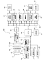
図1は本発明の実施形態であるCCD固体撮像素子を搭載したデジタルカメラのブロック図である。 FIG. 1 is a block diagram of a digital camera equipped with a CCD solid-state imaging device according to an embodiment of the present invention.
図1に示すように、本実施形態のデジタルカメラ(撮像装置)200は、撮影レンズ11と、固体撮像素子(CCD固体撮像素子)100と、この両者の間に設けられた絞り13と、赤外線カットフィルタ15と、光学ローパスフィルタ17とを備える。デジタルカメラ200の全体を統括制御するCPU19は、フラッシュ発光部21及び受光部23を制御し、レンズ駆動部25を制御して撮影レンズ11の位置をフォーカス位置に調整し(AF制御)、絞り駆動部27を介して絞り13の開口量を制御(AE制御)して露光量調整を行う。
As shown in FIG. 1, a digital camera (imaging device) 200 according to this embodiment includes a photographing lens 11, a solid-state imaging device (CCD solid-state imaging device) 100, a
また、CPU19は、撮像素子駆動部29を介して固体撮像素子100を駆動し、撮影レンズ11を通して撮像した被写体画像を色信号として出力させる。CPU19には、操作部31を通してユーザからの指示信号が入力され、CPU19はこの指示にしたがって各種制御を行う。
Further, the
デジタルカメラ200の電気制御系は、固体撮像素子100の出力に接続されたアナログ信号処理部33と、このアナログ信号処理部33から出力されたRGBの色信号をデジタル信号に変換するA/D変換回路35とを備え、これらはCPU19によって制御される。
The electric control system of the
さらに、このデジタルカメラ200の電気制御系は、メインメモリ(フレームメモリ)41に接続されたメモリ制御部43と、ガンマ補正演算,RGB/YC変換処理,画像合成処理等の画像処理を行うデジタル信号処理部45と、撮像画像をJPEG画像に圧縮したり圧縮画像を伸張したりする圧縮伸張処理部47と、測光データを積算しデジタル信号処理部45が行うホワイトバランス補正のゲインを求める積算部49と、着脱自在の記録媒体51が接続される外部メモリ制御部53と、カメラ背面等に搭載された表示部55が接続される表示制御部57と、を備え、これらは、制御バス61及びデータバス63によって相互に接続され、CPU19からの指令によって制御される。
Further, the electric control system of the
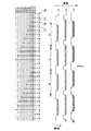
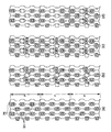
次に、固体撮像素子及びその駆動方法について図2から図4に基づいて説明する。図2は本発明に係る固体撮像素子の要部拡大平面図、図3は垂直電荷転送電極と転送信号、及びこれによる電位分布の様子を模式的に示す説明図、図4は固体撮像素子の駆動方法を示す模式図である。 Next, a solid-state imaging device and a driving method thereof will be described with reference to FIGS. 2 is an enlarged plan view of the main part of the solid-state imaging device according to the present invention, FIG. 3 is an explanatory diagram schematically showing the state of the vertical charge transfer electrode, the transfer signal, and the potential distribution thereby, and FIG. It is a schematic diagram which shows a drive method.
図2に示すように、本発明に係る固体撮像素子100は、多数の光電変換素子91が平面上に行方向(矢印Xの方向)及び列方向(矢印Yの方向)に沿って二次元配置された受光部95を有している。各々の光電変換素子91は、半導体で構成されるフォトダイオードを備えており、各々の受光面に入射した光の強さと露光時間の長さとで定まる光量に応じた信号電荷を生成する。
As shown in FIG. 2, in the solid-
二次元配置された多数の光電変換素子91のそれぞれが出力する信号電荷を、固体撮像素子100の出力端子から時系列のフレーム毎の信号として取り出すために、複数の垂直電荷転送部93と、水平電荷転送部71と、出力増幅器73とが、固体撮像素子100に備わっている。
In order to take out the signal charges output from each of the two-dimensionally arranged
各々の垂直電荷転送部93は、光電変換素子91と隣接する位置に、図中縦方向(矢印Y方向)に向かって延設されており、1列分の光電変換素子91のそれぞれから信号電荷を受け取った後、列毎に信号電荷を矢印Y方向に順次に転送する。
Each vertical
各列の垂直電荷転送部93の出力側には水平電荷転送部71が配置されており、垂直電荷転送部93から信号電荷が受け渡され、水平電荷転送部71上に1行分の信号電荷が転送される。水平電荷転送部71は、1行分の信号電荷を水平方向(矢印X方向)に順次に転送する。水平電荷転送部71の出力に順番に現れる信号電荷は、出力増幅器73で増幅され、出力端子OUTから出力される。
A horizontal
なお、垂直電荷転送部93と水平電荷転送部71との間にラインメモリ(図示せず)を配置して、各垂直電荷転送部93から同時に出力される1行分の信号電荷をラインメモリ上に一時的に蓄積し、該蓄積された1行分の信号電荷を、ラインメモリから水平電荷転送部71に向かって転送するようにしてもよい。
A line memory (not shown) is arranged between the vertical
このような読み出し動作を実現するのに必要な制御信号、すなわち、垂直転送制御信号φV1〜φV12(12相駆動)と、水平転送制御信号φH(図示せず)とが、撮像素子駆動部29(図1参照)に配設された図示しないタイミング信号発生回路によって生成され、固体撮像素子100の各垂直電荷転送部93と、水平電荷転送部71とにそれぞれ印加される。
Control signals necessary for realizing such a read operation, that is, vertical transfer control signals φV1 to φV12 (12-phase drive) and horizontal transfer control signal φH (not shown) are supplied to the image sensor drive unit 29 ( 1) and is applied to each vertical
多数の光電変換素子91は、ハニカム状のパターン(光電変換素子91の配置位置を各行毎で水平方向に半ピッチずらしたパターン)を形成するように配置されている。また、図2中に「G」、「B」、「R」で示すように、それぞれの光電変換素子91は検出する色成分が予め定められている。すなわち、「G」の各光電変換素子91は緑色成分、「B」の各光電変換素子91は青色成分、「R」の各光電変換素子91は赤色成分の明るさを検出する。これらの検出色は、各光電変換素子91の受光面の前面に配置された光学フィルタの分光特性によって設定される。
The large number of
図2に示す例では、一行毎に同色の色成分を検出する光電変換素子が行方向に沿って交互に配列される配列(ベイヤー配列)の各列がそれぞれ複数列配置されている(本明細書では「ダブルベイヤー配列」と呼称する)。即ち、図中上側からGRGR・・・及びBGBG・・・の順で1列毎に配列された第1光電変換素子列81と、第1光電変換素子列81に対して配列ピッチの1/2だけ水平及び垂直方向にずれた位置に配列された第2光電変換素子列83とが、行方向に繰り返し配列されている。
In the example shown in FIG. 2, a plurality of columns of an array (Bayer array) in which photoelectric conversion elements that detect color components of the same color for each row are alternately arranged in the row direction are arranged (this specification) (Referred to as “double Bayer arrangement”). That is, the first photoelectric
垂直電荷転送部93は、光電変換素子91の列毎に、各列と隣接する位置に蛇行する形状で形成されている。各々の垂直電荷転送部93は、半導体基板に形成された垂直電荷転送チャネル75と、半導体基板上に電気的絶縁膜(図示せず)を介して配置された電荷転送用の多数本の第1垂直転送電極77、第2垂直転送電極79とを備えている。
The vertical
すなわち、各電極77,79に所定の電圧を印加して各垂直電荷転送チャネル75上に所定の電位分布を形成し、各電極に印加する電圧を順次に切り替えることにより、垂直電荷転送部93(垂直電荷転送チャネル75)において各画素の信号電荷を目的の方向に向けて順次に転送することができる。
That is, by applying a predetermined voltage to each of the
第1垂直転送電極77及び第2垂直転送電極79は、光電変換素子91の行毎にそれぞれ1つずつ形成されている。なお、各第1垂直転送電極77は、光電変換素子91から垂直電荷転送部93の垂直電荷転送チャネル75への信号電荷の転送を制御するための読出しゲートとしても機能する。
One first
矢印Y方向に交互に並んでいる第2垂直転送電極79及び第1垂直転送電極77のそれぞれには、12相の垂直転送制御信号(あるいは駆動パルスと呼ぶ)φV1〜φV12のいずれかが各第2垂直転送電極79及び第1垂直転送電極77の配置された位置関係に応じて印加される。
Each of the second
図3に示すように、それぞれの垂直電荷転送チャネル75(垂直電荷転送部93)は、3行分の光電変換素子91に対応して1つの電荷蓄積パケットPが配置されて、複数の電荷蓄積パケットPが形成されており、3行分の光電変換素子91から読み出された信号電荷は、それぞれの1つの電荷蓄積パケットPにまとめて蓄積される。電荷蓄積パケットPに蓄積された3行分の信号電荷は、図3のタイミングチャートに示すように、12相の垂直転送制御信号φV1〜φV12に同期して電荷蓄積パケットPごとに垂直方向に転送される。
As shown in FIG. 3, in each vertical charge transfer channel 75 (vertical charge transfer unit 93), one charge storage packet P is arranged corresponding to three rows of
次に、図4を参照して、固体撮像素子の駆動方法について説明する。なお、以下の各実施形態において、正方形枠は各光電変換素子91を示し、R、G、Bが書かれた小円は各色成分の信号電荷を示す。正方形枠内に小円が記載されている場合は光電変換素子91に各色の信号電荷がある状態を、小円が記載されていない場合は光電変換素子91に信号電荷がない状態を示す。また、正方形枠右下隅の長方形枠は、各光電変換素子91から垂直電荷転送チャネル75(電荷蓄積パケットP)へ信号電荷を読み出す読出しゲートを示す。
Next, a method for driving the solid-state imaging device will be described with reference to FIG. In each of the following embodiments, a square frame indicates each
本実施形態において、垂直電荷転送チャネル75は、図中、縦方向に3個の光電変換素子91に対して1つの電荷蓄積パケットPが対応するように区分されている。また、同図(a)から(e)は時間経過に従って信号電荷が転送される状態を示す。
In the present embodiment, the vertical
図4(a)に示すように、固体撮像素子100は、各光電変換素子91が一定時間露光されて各色の信号電荷が蓄積される。ここで、それぞれの電荷蓄積パケットPに対する奇数行(1行目及び3行目)の光電変換素子91に読み出し電圧を印加すると、それぞれの電荷蓄積パケットPには、同色の色成分の2つの信号電荷が読み出される図4(b−1)。即ち、図中左から1列目と2列目の各電荷蓄積パケットPには、上から順に2つのR信号電荷、2つのG信号電荷、2つのR信号電荷、・・・が、また、3列目と4列目の各電荷蓄積パケットPには、上から順に2つのG信号電荷、2つのB信号電荷、2つのG信号電荷、・・・が読み出され、各電荷蓄積パケットP内で電荷加算される(図4(b−2))。ここでは、電荷加算された2つの信号電荷は、それぞれ2R、2G、2Bと表記する。
なお、本明細書においては、各列において、それぞれの光電変換素子91に対応して「行」を定義する。すなわち、電荷転送方向上流側から順に1行目、2行目、・・・となり、隣接する列同士では、同一行が斜めに配置されることになる。
As shown in FIG. 4A, in the solid-
In this specification, in each column, a “row” is defined corresponding to each
次いで、図4(c)に示すように、各色成分の信号電荷2R、2G、2Bが読み出された電荷蓄積パケットPは、垂直電荷転送チャネル75を1パケット分だけ垂直転送される。これにより、各色成分の信号電荷2R、2G、2Bを有するそれぞれの電荷蓄積パケットPは、同一色R、G、Bの信号電荷が読み出されずに残っている光電変換素子91に対応する位置に位置する。
Next, as shown in FIG. 4C, the charge accumulation packet P from which the signal charges 2R, 2G, and 2B of the respective color components have been read is vertically transferred by one packet through the vertical
ここで、図4(d)に示すように、信号電荷R、G、Bが残っている光電変換素子91から各電荷蓄積パケットPに信号電荷R、G、Bを読み出すと、それぞれの電荷蓄積パケットPには、該電荷蓄積パケットPが有する信号電荷2R、2G、2Bと同一色成分の信号電荷R、G、Bが読み出されて該電荷蓄積パケットP内で電荷加算され、各電荷蓄積パケットPには同一色成分の3つの信号電荷R、G、Bが電荷加算された信号電荷3R、3G、3Bが読み出される。換言すれば、全ての光電変換素子91の信号電荷R、G、Bは、同一色成分ごとに電荷加算されて該電荷蓄積パケットPに読み出される(図4(e))。
Here, as shown in FIG. 4D, when the signal charges R, G, and B are read out from the
そして、電荷加算された信号電荷3R、3G、3Bは、垂直電荷転送部93を垂直方向に転送されて水平電荷転送部71に受け渡され、更に水平電荷転送部71が水平方向に順次転送して出力増幅器73で増幅し、出力端子OUTから出力される。このような駆動方法に基づく信号処理は、信号処理手段である撮像素子駆動部29からの指令に基づいて行われる(図1参照)。
Then, the signal charges 3R, 3G, and 3B after the charge addition are transferred in the vertical direction by the vertical
上記したように、光電変換素子91の信号電荷R、G、Bは捨てられることなく、全ての光電変換素子91の信号電荷R、G、Bが同一色成分ごとに電荷加算されて出力されるので、固体撮像素子100の高感度化が可能となる。また、このような固体撮像素子100を備える撮像装置200によれば、ムービー画像の撮像、AE/AF制御のいずれかを行うとき、上記した信号処理の駆動方法に切り替えて、高感度で画像取込みを行うことができ、光量の不足する撮影シーンであっても高感度のムービー画像が得られる。また、精度よく適正化されたAE/AFで撮像することができる。
As described above, the signal charges R, G, and B of the
(第2実施形態)
上記した固体撮像素子の駆動方法は、1つ毎に同一色の光電変換素子91が、縦方向に配列された固体撮像素子100を用い、3以上の奇数行の光電変換素子91から、対応する電荷蓄積パケットPに信号電荷R、G、Bを読み出すことによって達成することができる。図5及び図6は第2実施形態の固体撮像素子の駆動方法を示す模式図であり、図5は前半部を、図6は後半部を示す。
(Second Embodiment)
The above-described solid-state image sensor driving method uses the solid-
図5及び図6に示すように、第2実施形態の固体撮像素子は、垂直電荷転送チャネル75が、図中縦方向に配列された5個の光電変換素子91に対して1つの電荷蓄積パケットPが対応するように区分されている。
As shown in FIGS. 5 and 6, in the solid-state imaging device of the second embodiment, the vertical
図5(a)に示すように、それぞれの電荷蓄積パケットPに対する奇数行(1行目、3行目及び5行目)の光電変換素子91に読み出し電圧を印加すると、それぞれの電荷蓄積パケットPには、同色の色成分の信号電荷が読み出されて、各電荷蓄積パケットP内で電荷加算される(図5(b1))。即ち、各電荷蓄積パケットPは、3つの光電変換素子91から読み出された信号電荷が電荷加算されて信号電荷3R、3G、3Bとなる(図5(b2))。ここで、図6(c)に示すように、各色成分の信号電荷3R、3G、3Bを有する各電荷蓄積パケットPを、垂直電荷転送チャネル75で1パケット分だけ垂直転送すると、該電荷蓄積パケットPは、同一色R、G、Bの信号電荷が読み出されずに残っている2つの光電変換素子91に対応する位置に位置する。
As shown in FIG. 5A, when a read voltage is applied to the
次いで、図6(d)に示すように、それぞれ信号電荷R、G、Bが残っている2つの光電変換素子91から各電荷蓄積パケットPに信号電荷R、G、Bを読み出すと、それぞれの電荷蓄積パケットPには、同一色成分の2つの信号電荷R、G、Bが更に読み出されて、該電荷蓄積パケットP内で電荷加算される。これにより、各電荷蓄積パケットPには、同一色成分の5つの信号電荷R、G、Bが電荷加算された信号電荷5R、5G、5Bが読み出される(図6(e))。
Next, as shown in FIG. 6D, when the signal charges R, G, and B are read out from the two
以後、第1実施形態の固体撮像素子100と同様に、電荷加算された信号電荷5R、5G、5Bは、垂直電荷転送部93及び水平電荷転送部71を順次、垂直方向及び水平方向に転送され、出力増幅器73で増幅されて出力端子OUTから出力する。
Thereafter, similarly to the solid-
上記した固体撮像素子の駆動方法は、原理的には、同一色成分の信号電荷を有する奇数行の信号電荷を、同一の電荷蓄積パケットPに読み出して電荷加算し、1パケット分垂直転送した後、読み出されずに残っている信号電荷を更に読み出して電荷加算することにより、電荷加算する光電変換素子91の数に拘わらず可能ではあるが、実質的には電荷加算する光電変換素子91の数が増加すると画質が低下するので、電荷加算する光電変換素子91の数は、3素子または5素子程度とするのが好ましく、更には3素子が好ましい。
本構成の場合は、5素子の信号電荷が加算されるため、信号電荷量を増加でき、一層の高感度化が図られる。その他の作用効果は、第1実施形態の固体撮像素子と同様である。
In principle, the solid-state image sensor driving method described above is to read out the signal charges in odd rows having the same color component signal charge to the same charge accumulation packet P, add the charges, and vertically transfer one packet. This is possible regardless of the number of
In the case of this configuration, since the signal charges of five elements are added, the amount of signal charges can be increased, and higher sensitivity can be achieved. Other functions and effects are the same as those of the solid-state imaging device of the first embodiment.
(第3実施形態)
上記した第1、2実施形態においては、垂直電荷転送部93(垂直電荷転送チャネル75)で信号電荷を電荷加算する例について説明したが、水平電荷転送部で信号電荷を電荷加算することもできる。図7及び図8は水平電荷転送部で信号電荷を電荷加算する固体撮像素子の駆動方法を示す模式図であり、図7は同色成分の信号荷電が連続するように垂直電荷転送部に読み出される状態を示す模式図、図8は連続する同色成分の信号荷電が水平電荷転送部(ラインメモリ)で電荷加算される状態を示す模式図である。
(Third embodiment)
In the first and second embodiments described above, the example in which the signal charge is added by the vertical charge transfer unit 93 (vertical charge transfer channel 75) has been described. However, the signal charge can also be added by the horizontal charge transfer unit. . 7 and 8 are schematic diagrams showing a driving method of a solid-state imaging device in which signal charges are added by a horizontal charge transfer unit, and FIG. 7 is read to the vertical charge transfer unit so that signal charges of the same color component are continuous. FIG. 8 is a schematic diagram showing a state in which signal charges of continuous same color components are added by a horizontal charge transfer unit (line memory).
図7及び図8に示すように、第3実施形態の固体撮像素子100は、一行毎に同色の色成分を検出する光電変換素子91が列方向に沿って交互に配列されている。また、垂直電荷転送チャネル75が、1個の光電変換素子91に対して1つの電荷蓄積パケットPが対応するように区分されている。
As shown in FIGS. 7 and 8, in the solid-
図7(a)に示すように、一行毎に同色の信号電荷が列方向に沿って交互に配列された(RGRG・・、及びGBGB・・)光電変換素子91の信号電荷を、列方向に沿って2行の読み込み、1行の非読み込みを順次繰り返す。これにより、1行分の空白電荷パケットPBが、3行ごとに出現して垂直電荷チャネル75に離散配置される(図7(b))。 As shown in FIG. 7A, the signal charges of the photoelectric conversion elements 91 (RGRG ·· and GBGB ··) in which the same color signal charges are alternately arranged in the column direction for each row are arranged in the column direction. 2 rows are read along, and 1 row is not read sequentially. As a result, blank charge packets PB for one row appear every three rows and are discretely arranged in the vertical charge channel 75 (FIG. 7B).
次いで、図7(c)に示すように、垂直電荷転送チャネル75の信号電荷を3行分転送すると、垂直電荷チャネル75の空白電荷パケットPBは、信号電荷が読み出されずに残っている光電変換素子91に対応する位置に位置する。読み出されずに残っている光電変換素子91の信号電荷は、空白電荷パケットPBの前後の電荷蓄積パケットPに読み出された色と同色となる。ここで、図7(d)に示すように、信号電荷が残っている光電変換素子91から信号電荷を空白電荷パケットPBに読み出すと、垂直電荷チャネル75には同一色成分の信号電荷R、G、Bが3つ連続した状態で読み出される。具体的には、図8(a)に示すように、1、2列目の垂直電荷転送チャネル75には、RRRGGGRRR・・の順で、また3、4列目の垂直電荷転送チャネル75には、GGGBBBGGG・・の順で、3つの同一色成分の信号電荷が連続する。
Next, as shown in FIG. 7C, when the signal charge of the vertical
垂直電荷転送チャネル75の3行分の信号電荷を垂直方向に転送して、ラインメモリ85で同一色成分の信号電荷同士を電荷加算(3R、3G、3B)した後(図8(b))、水平電荷転送部71へ受け渡す(図8(c))。水平電荷転送部71は、電荷加算された信号電荷3R、3G、3Bを順次、水平方向に転送して出力する(図8(d))。
After the signal charges for three rows of the vertical
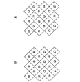
なお、上記の説明においては、光電変換素子の各色成分が、図9(a)に示すように配列されたダブルベイヤー配列について説明したが、図9(b)に示すようにベイヤー配列を45度傾斜させて配置した固体撮像素子についても同様の駆動方法を採用することができ、同様の効果を奏する。
その他の作用、効果は、第1実施形態の固体撮像素子と同様であるので、説明を省略する。なお、上記の実施形態においては、信号電荷の電荷加算をラインメモリ85で行っているが、水平電荷転送部71で行うようにしてもよい。
In the above description, the double Bayer arrangement in which the color components of the photoelectric conversion elements are arranged as shown in FIG. 9A has been described. However, as shown in FIG. A similar driving method can be adopted for a solid-state imaging device arranged in an inclined manner, and the same effect can be obtained.
Since other operations and effects are the same as those of the solid-state imaging device of the first embodiment, the description thereof is omitted. In the above embodiment, the signal charge is added by the
(対比例)
次に、上記した第1、2、3実施形態の駆動方法と比較するため、対比例の駆動方法について図10及び図11に基づいて簡単に説明する。図10は第1対比例の固体撮像素子の駆動方法を示す模式図、図11は第2対比例の固体撮像素子の駆動方法を示す模式図である。
(Comparison)
Next, for comparison with the driving methods of the first, second, and third embodiments described above, a comparative driving method will be briefly described with reference to FIGS. 10 and 11. FIG. 10 is a schematic diagram showing a driving method of the first proportional solid-state imaging device, and FIG. 11 is a schematic diagram showing a driving method of the second proportional solid-state imaging device.
図10(a)に示すように、第1対比例の固体撮像素子は、垂直電荷転送チャネル75が、図中縦方向に配列された3個の光電変換素子91に対して1つの電荷蓄積パケットPが対応するように区分されている。
As shown in FIG. 10A, in the first proportional solid-state imaging device, the vertical
第1対比例の固体撮像素子の駆動方法は、図10(b)に示すように、光電変換素子91の信号電荷を、列方向に沿って1行の読み込み、2行の非読み込みを順次繰り返す。これにより、図中左から順に、第1及び第2列目の各電荷蓄積パケットPには、G、R、G、・・の順で、また第3及び第4列目の各電荷蓄積パケットPには、B、G、B、・・の順で信号電荷が読み出される。そして、信号電荷を1パケット分ずつ垂直方向に転送して(図10(c)、(d))、水平電荷転送部71に受け渡し、更に水平方向に転送して出力する。
As shown in FIG. 10B, the first proportional solid-state image sensor driving method sequentially reads signal charges of the
第1対比例の固体撮像素子の駆動方法によると、光電変換素子91に蓄積された信号電荷のうち、1/3の信号電荷だけが使用され、2/3の信号電荷が捨てられるので、感度の低い画像となるが、高速での信号処理が可能となる。
According to the first proportional solid-state image sensor driving method, only 1/3 of the signal charge accumulated in the
また、図11(a)に示すように、第2対比例の固体撮像素子は、垂直電荷転送チャネル75が、図中縦方向に配列された3個の光電変換素子91に対して1つの電荷蓄積パケットPが対応するように区分されている。
As shown in FIG. 11A, the second proportional solid-state imaging device has one charge for three
第2対比例の固体撮像素子の駆動方法は、図11(b‐1)に示すように、光電変換素子91の信号電荷を、列方向に沿って2行の読み込み、1行の非読み込みを順次繰り返す。これにより、各電荷蓄積パケットPには、同一色成分の2つの信号電荷が読み出されて電荷加算される。具体的には、図中左から第1及び第2列目の各電荷蓄積パケットPには、2R、2G、2R・・の順で、また第3及び第4列目の各電荷蓄積パケットPには、2G、2B、2G・・の順で信号電荷が読み出される(図11(b‐2))。
As shown in FIG. 11 (b-1), the second proportional solid-state image sensor driving method reads the signal charges of the
読み出された信号電荷2R、2G、2Bは、1パケット分ずつ垂直方向に転送されて(図11(c)、(d))、水平電荷転送部71に受け渡され、更に水平電荷転送部71で水平方向に転送されて出力される。
The read signal charges 2R, 2G, and 2B are transferred in the vertical direction by one packet (FIGS. 11C and 11D), transferred to the horizontal
第2対比例の固体撮像素子の駆動方法によると、光電変換素子91に蓄積された信号電荷のうち、2/3の信号電荷が使用され、1/3の信号電荷は捨てられるので、第1対比例の駆動方法より感度は高くなる。
According to the second proportional solid-state imaging device driving method, 2/3 of the signal charges accumulated in the
なお、本発明に係る固体撮像素子の駆動方法及び撮像装置は、前述した各実施形態に限定されるものではなく、適宜、変形や改良等が可能である。 Note that the solid-state imaging device driving method and imaging apparatus according to the present invention are not limited to the above-described embodiments, and can be modified or improved as appropriate.
本発明によれば、ムービー画像の撮像やAE/AF制御の信号駆動において、全画素の信号電荷を使用し、これによって、より高感度のムービー画像やAE/AF画像が得られる固体撮像素子の駆動方法及び撮像装置を提供することができる。 According to the present invention, a solid-state imaging device that uses signal charges of all pixels in movie image capturing and AE / AF control signal driving, thereby obtaining a movie image or AE / AF image with higher sensitivity. A driving method and an imaging apparatus can be provided.
11 撮影レンズ(光学系)
13 絞り(光学系)
15 赤外線カットフィルタ(光学系)
17 光学ローパスフィルタ(光学系)
71 水平電荷転送部
81 第1光電変換素子列
83 第2光電変換素子列
85 ラインメモリ
91 光電変換素子
93 垂直電荷転送部
95 受光部
100 固体撮像素子
200 デジタルカメラ(撮像装置)
P 電荷蓄積パケット
PB 空白電荷パケット
R、G、B 信号電荷
11 Shooting lens (optical system)
13 Aperture (optical system)
15 Infrared cut filter (optical system)
17 Optical low-pass filter (optical system)
71 horizontal
P Charge storage packet PB Blank charge packet R, G, B Signal charge
Claims (6)
前記垂直電荷転送部に対して、3以上の奇数行分の光電変換素子からの信号電荷を蓄積する1つの電荷蓄積パケットを複数形成し、
前記電荷蓄積パケットのそれぞれに、前記画素部の光電変換素子から同色同士の信号電荷を複数行分読み出して電荷加算した後、
前記垂直電荷転送部の信号電荷を前記電荷蓄積パケット一つ分だけ転送し、
前記電荷蓄積パケットに読み出された色と同色となる前記垂直電荷転送部に残された信号電荷を、前記電荷蓄積パケットに読み出して再度電荷加算する固体撮像素子の駆動方法。 A light receiving unit in which a plurality of photoelectric conversion elements are arranged in a two-dimensional matrix on a semiconductor substrate, and a signal charge generated by the photoelectric conversion elements arranged adjacent to each other along the column direction of the photoelectric conversion elements are read out. A plurality of vertical charge transfer units that transfer in the vertical direction; and a horizontal charge transfer unit that transfers signal charges transferred from the vertical charge transfer unit in the horizontal direction, wherein the light receiving unit has at least three different color components. A method for driving a solid-state imaging device in which photoelectric conversion elements to be detected are dispersedly arranged, and one charge storage for storing signal charges from photoelectric conversion elements for three or more odd rows in the vertical charge transfer unit Form multiple packets,
After each of the charge accumulation packets is read out from the photoelectric conversion element of the pixel unit for a plurality of rows of signal charges of the same color, the charge is added.
Transfer the signal charge of the vertical charge transfer unit by one charge storage packet,
A method for driving a solid-state imaging device, wherein the signal charge remaining in the vertical charge transfer unit having the same color as the color read in the charge accumulation packet is read out to the charge accumulation packet and added again.
前記受光部の光電変換素子は、一行毎に同色の色成分を検出する光電変換素子が列方向に沿って交互に配列されている固体撮像素子の駆動方法。 A method for driving a solid-state imaging device according to claim 1,
The photoelectric conversion element of the light receiving unit is a method for driving a solid-state imaging element in which photoelectric conversion elements for detecting the same color component for each row are alternately arranged along the column direction.
前記受光部の光電変換素子は、一行毎に同色の色成分を検出する光電変換素子が列方向に沿って交互に配列された第1光電変換素子列と、該第1光電変換素子列に対して配列ピッチの1/2だけ水平及び垂直方向にずれた位置に配列された第2光電変換素子列と、を行方向に繰り返し配列されている固体撮像素子の駆動方法。 A method for driving a solid-state imaging device according to claim 1,
The photoelectric conversion element of the light receiving unit includes a first photoelectric conversion element array in which photoelectric conversion elements for detecting the same color component for each row are alternately arranged in the column direction, and the first photoelectric conversion element array And a second photoelectric conversion element array arranged at a position displaced in the horizontal and vertical directions by ½ of the arrangement pitch, and a method for driving the solid-state imaging element, which is repeatedly arranged in the row direction.
前記垂直電荷転送部に対して、前記光電変換素子の信号電荷を前記列方向に沿って2行の読み込み、1行の非読み込みを順次繰り返して1行分の空白電荷パケットを前記垂直電荷転送部に離散配置した後、
前記垂直電荷転送部の信号電荷を3行分転送し、
前記垂直電荷転送部の前記空白電荷パケットに、該空白電荷パケットの前後の電荷パケットに読み出された色と同色となる前記垂直電荷転送部に残された信号電荷を読み出し、
これにより得られる3つの連続する色成分の信号電荷を前記ラインメモリまたは前記水平電荷転送部で電荷加算して転送する固体撮像素子の駆動方法。 A light receiving unit in which a plurality of photoelectric conversion elements are arranged in a two-dimensional matrix on a semiconductor substrate, and a signal charge generated by the photoelectric conversion elements arranged adjacent to each other along the column direction of the photoelectric conversion elements are read out. A plurality of vertical charge transfer units that transfer in the vertical direction, a horizontal charge transfer unit that transfers signal charges transferred from the vertical charge transfer unit in the horizontal direction, and between the vertical charge transfer unit and the horizontal charge transfer unit A solid-state imaging device in which the photoelectric conversion elements of the light receiving unit are arranged alternately in the column direction to detect color components of the same color for each row. A method,
For the vertical charge transfer unit, the signal charge of the photoelectric conversion element is read in two rows along the column direction, and the non-reading of one row is sequentially repeated so that a blank charge packet for one row is transferred to the vertical charge transfer unit. After the discrete placement in
Transfer the signal charges of the vertical charge transfer unit for three rows
Read the signal charge left in the vertical charge transfer unit, which is the same color as the color read in the charge packets before and after the blank charge packet, to the blank charge packet of the vertical charge transfer unit,
A method for driving a solid-state imaging device, wherein signal charges of three continuous color components obtained thereby are added and transferred by the line memory or the horizontal charge transfer unit.
請求項1〜請求項4のいずれか1項記載の固体撮像素子の駆動方法に基づいて信号処理する信号処理手段と、
前記固体撮像素子に光学像を結像させる光学系と、
を備えた撮像装置。 A light receiving unit in which a plurality of photoelectric conversion elements are arranged in a two-dimensional matrix on a semiconductor substrate, and a signal charge generated by the photoelectric conversion elements arranged adjacent to each other along the column direction of the photoelectric conversion elements are read out. A plurality of vertical charge transfer units that transfer in the vertical direction, and a horizontal charge transfer unit that transfers the signal charges transferred from the vertical charge transfer unit in the horizontal direction,
Signal processing means for performing signal processing based on the solid-state imaging device driving method according to any one of claims 1 to 4,
An optical system for forming an optical image on the solid-state imaging device;
An imaging apparatus comprising:
Priority Applications (2)
| Application Number | Priority Date | Filing Date | Title |
|---|---|---|---|
| JP2007231913A JP2009065478A (en) | 2007-09-06 | 2007-09-06 | Driving method of solid-state image sensor, and imaging apparatus |
| US12/204,513 US7952636B2 (en) | 2007-09-06 | 2008-09-04 | Method for driving solid-state imaging device and imaging apparatus |
Applications Claiming Priority (1)
| Application Number | Priority Date | Filing Date | Title |
|---|---|---|---|
| JP2007231913A JP2009065478A (en) | 2007-09-06 | 2007-09-06 | Driving method of solid-state image sensor, and imaging apparatus |
Publications (2)
| Publication Number | Publication Date |
|---|---|
| JP2009065478A true JP2009065478A (en) | 2009-03-26 |
| JP2009065478A5 JP2009065478A5 (en) | 2010-04-15 |
Family
ID=40431440
Family Applications (1)
| Application Number | Title | Priority Date | Filing Date |
|---|---|---|---|
| JP2007231913A Withdrawn JP2009065478A (en) | 2007-09-06 | 2007-09-06 | Driving method of solid-state image sensor, and imaging apparatus |
Country Status (2)
| Country | Link |
|---|---|
| US (1) | US7952636B2 (en) |
| JP (1) | JP2009065478A (en) |
Families Citing this family (9)
| Publication number | Priority date | Publication date | Assignee | Title |
|---|---|---|---|---|
| ES2486295T3 (en) | 2007-04-11 | 2014-08-18 | Red.Com, Inc. | Video camera |
| US8237830B2 (en) | 2007-04-11 | 2012-08-07 | Red.Com, Inc. | Video camera |
| US8149323B2 (en) * | 2008-12-18 | 2012-04-03 | Qualcomm Incorporated | System and method to autofocus assisted by autoexposure control |
| US8576319B2 (en) * | 2009-12-25 | 2013-11-05 | Japan Atomic Energy Agency | Image sensor, semiconductor device and image sensing method |
| US20110317048A1 (en) * | 2010-06-29 | 2011-12-29 | Aptina Imaging Corporation | Image sensor with dual layer photodiode structure |
| JPWO2013084406A1 (en) * | 2011-12-08 | 2015-04-27 | パナソニックIpマネジメント株式会社 | Solid-state imaging device and imaging device |
| WO2013100034A1 (en) * | 2011-12-27 | 2013-07-04 | 富士フイルム株式会社 | Color imaging element |
| WO2014127153A1 (en) | 2013-02-14 | 2014-08-21 | Red. Com, Inc. | Video camera |
| WO2019010233A1 (en) | 2017-07-05 | 2019-01-10 | Red. Com, Llc | Video image data processing in electronic devices |
Family Cites Families (10)
| Publication number | Priority date | Publication date | Assignee | Title |
|---|---|---|---|---|
| JP3511772B2 (en) * | 1995-12-21 | 2004-03-29 | ソニー株式会社 | Solid-state imaging device, driving method of solid-state imaging device, camera device and camera system |
| JPH10136244A (en) * | 1996-11-01 | 1998-05-22 | Olympus Optical Co Ltd | Electronic image pickup device |
| JPH11234569A (en) * | 1998-02-13 | 1999-08-27 | Sony Corp | Drive method for solid-state image pickup device, solid-state image pickup element and camera |
| JP4140077B2 (en) * | 1998-02-18 | 2008-08-27 | ソニー株式会社 | Solid-state image sensor driving method, solid-state image sensor, and camera |
| JP2894341B1 (en) | 1998-03-12 | 1999-05-24 | 日本電気株式会社 | Driving method of solid-state imaging device |
| JP4307780B2 (en) * | 2002-03-07 | 2009-08-05 | 富士フイルム株式会社 | Solid-state imaging device and signal reading method thereof |
| JP4139641B2 (en) | 2002-07-19 | 2008-08-27 | 富士フイルム株式会社 | Solid-state image sensor |
| US7385638B2 (en) * | 2004-04-28 | 2008-06-10 | Eastman Kodak Company | Image sensor for still or video photography |
| US7570290B2 (en) * | 2004-12-27 | 2009-08-04 | Sony Corporation | Drive method for solid-state imaging device, solid-state imaging device, and imaging apparatus |
| US7636119B2 (en) * | 2005-12-21 | 2009-12-22 | Eastman Kodak Company | Image sensor for still or video photography |
-
2007
- 2007-09-06 JP JP2007231913A patent/JP2009065478A/en not_active Withdrawn
-
2008
- 2008-09-04 US US12/204,513 patent/US7952636B2/en not_active Expired - Fee Related
Also Published As
| Publication number | Publication date |
|---|---|
| US20090066827A1 (en) | 2009-03-12 |
| US7952636B2 (en) | 2011-05-31 |
Similar Documents
| Publication | Publication Date | Title |
|---|---|---|
| JP4448888B2 (en) | Imaging apparatus and signal processing method of imaging apparatus | |
| US8054342B2 (en) | Imaging apparatus and method for driving the imaging apparatus | |
| US7944496B2 (en) | Imaging apparatus and driving method for CCD type solid-state imaging device | |
| US8908064B2 (en) | Imaging apparatus and imaging method | |
| JP4951440B2 (en) | Imaging apparatus and solid-state imaging device driving method | |
| JP2009065478A (en) | Driving method of solid-state image sensor, and imaging apparatus | |
| JP2008104013A (en) | Driving method of solid-state imaging element and imaging apparatus | |
| US20110216228A1 (en) | Solid-state image sensing element, method for driving solid-state image sensing element and image pickup device | |
| JP2010130343A (en) | Imaging apparatus and its drive control method | |
| JP5033711B2 (en) | Imaging device and driving method of imaging device | |
| JP4538337B2 (en) | Solid-state image sensor | |
| JP2011244351A (en) | Imaging apparatus and drive control method of solid state image sensor | |
| JP4637033B2 (en) | Output bifurcated solid-state imaging device and imaging apparatus | |
| JP5124549B2 (en) | Moving image signal readout method and imaging apparatus for solid-state imaging device | |
| JP2007221457A (en) | Two branch output solid state image sensor and imaging apparatus | |
| JP2007235888A (en) | Single-ccd color solid-state imaging element and imaging apparatus | |
| JP2009303020A (en) | Image capturing apparatus and defective pixel correcting method | |
| JP2008148022A (en) | Method for driving solid-state image pickup device and imaging apparatus | |
| JP5256084B2 (en) | Imaging device and driving method of imaging device | |
| JP2008301328A (en) | Ccd solid-state imaging element and driving method thereof, and imaging element | |
| JP5175783B2 (en) | Imaging device and driving method of imaging device | |
| JP2009147540A (en) | Imaging device | |
| JP2009049504A (en) | Imaging device and imaging unit | |
| JP2009141404A (en) | Drive control method for ccd solid-state imaging sensor and imaging apparatus | |
| JP2009049523A (en) | Solid-state image sensor, imaging apparatus, and method for driving solid-state image sensor |
Legal Events
| Date | Code | Title | Description |
|---|---|---|---|
| A621 | Written request for application examination |
Free format text: JAPANESE INTERMEDIATE CODE: A621 Effective date: 20100224 |
|
| A521 | Request for written amendment filed |
Free format text: JAPANESE INTERMEDIATE CODE: A523 Effective date: 20100225 |
|
| A761 | Written withdrawal of application |
Free format text: JAPANESE INTERMEDIATE CODE: A761 Effective date: 20110606 |