JP4441578B2 - Electronic device and control method thereof - Google Patents
Electronic device and control method thereof Download PDFInfo
- Publication number
- JP4441578B2 JP4441578B2 JP2008538681A JP2008538681A JP4441578B2 JP 4441578 B2 JP4441578 B2 JP 4441578B2 JP 2008538681 A JP2008538681 A JP 2008538681A JP 2008538681 A JP2008538681 A JP 2008538681A JP 4441578 B2 JP4441578 B2 JP 4441578B2
- Authority
- JP
- Japan
- Prior art keywords
- heat
- infrared
- heat sensitive
- contact
- unit
- Prior art date
- Legal status (The legal status is an assumption and is not a legal conclusion. Google has not performed a legal analysis and makes no representation as to the accuracy of the status listed.)
- Active
Links
- 238000000034 method Methods 0.000 title claims description 60
- 238000010521 absorption reaction Methods 0.000 claims description 100
- 239000000758 substrate Substances 0.000 claims description 80
- 230000008859 change Effects 0.000 claims description 64
- 238000001514 detection method Methods 0.000 claims description 55
- 230000001965 increasing effect Effects 0.000 claims description 18
- 238000009429 electrical wiring Methods 0.000 claims description 6
- 239000012212 insulator Substances 0.000 claims description 6
- 239000004065 semiconductor Substances 0.000 claims description 6
- 230000001678 irradiating effect Effects 0.000 claims description 4
- 230000000704 physical effect Effects 0.000 claims description 3
- 230000006903 response to temperature Effects 0.000 claims 1
- 230000006698 induction Effects 0.000 description 26
- 230000035945 sensitivity Effects 0.000 description 16
- 238000009413 insulation Methods 0.000 description 15
- 206010047571 Visual impairment Diseases 0.000 description 14
- 239000003990 capacitor Substances 0.000 description 12
- 239000006096 absorbing agent Substances 0.000 description 11
- 230000004044 response Effects 0.000 description 10
- 230000007704 transition Effects 0.000 description 9
- 238000005338 heat storage Methods 0.000 description 7
- 230000006870 function Effects 0.000 description 6
- 239000000463 material Substances 0.000 description 6
- 238000001816 cooling Methods 0.000 description 4
- 230000000694 effects Effects 0.000 description 4
- 229910052751 metal Inorganic materials 0.000 description 4
- 239000002184 metal Substances 0.000 description 4
- 230000002093 peripheral effect Effects 0.000 description 4
- 229910004298 SiO 2 Inorganic materials 0.000 description 3
- 229910052782 aluminium Inorganic materials 0.000 description 3
- XAGFODPZIPBFFR-UHFFFAOYSA-N aluminium Chemical compound [Al] XAGFODPZIPBFFR-UHFFFAOYSA-N 0.000 description 3
- 238000010586 diagram Methods 0.000 description 3
- 230000036544 posture Effects 0.000 description 3
- 230000001681 protective effect Effects 0.000 description 3
- VYPSYNLAJGMNEJ-UHFFFAOYSA-N Silicium dioxide Chemical compound O=[Si]=O VYPSYNLAJGMNEJ-UHFFFAOYSA-N 0.000 description 2
- 238000003491 array Methods 0.000 description 2
- 230000006378 damage Effects 0.000 description 2
- 230000007423 decrease Effects 0.000 description 2
- 230000001419 dependent effect Effects 0.000 description 2
- 239000003302 ferromagnetic material Substances 0.000 description 2
- 239000011810 insulating material Substances 0.000 description 2
- 230000007246 mechanism Effects 0.000 description 2
- 230000002265 prevention Effects 0.000 description 2
- 230000005855 radiation Effects 0.000 description 2
- 238000004904 shortening Methods 0.000 description 2
- 229910052814 silicon oxide Inorganic materials 0.000 description 2
- RTAQQCXQSZGOHL-UHFFFAOYSA-N Titanium Chemical compound [Ti] RTAQQCXQSZGOHL-UHFFFAOYSA-N 0.000 description 1
- XHCLAFWTIXFWPH-UHFFFAOYSA-N [O-2].[O-2].[O-2].[O-2].[O-2].[V+5].[V+5] Chemical compound [O-2].[O-2].[O-2].[O-2].[O-2].[V+5].[V+5] XHCLAFWTIXFWPH-UHFFFAOYSA-N 0.000 description 1
- 230000002745 absorbent Effects 0.000 description 1
- 239000002250 absorbent Substances 0.000 description 1
- 230000009471 action Effects 0.000 description 1
- 230000008901 benefit Effects 0.000 description 1
- 150000001875 compounds Chemical class 0.000 description 1
- 229920001940 conductive polymer Polymers 0.000 description 1
- 239000000470 constituent Substances 0.000 description 1
- 239000013078 crystal Substances 0.000 description 1
- 238000005520 cutting process Methods 0.000 description 1
- 238000006073 displacement reaction Methods 0.000 description 1
- 238000009826 distribution Methods 0.000 description 1
- 238000001312 dry etching Methods 0.000 description 1
- 230000001939 inductive effect Effects 0.000 description 1
- 238000003331 infrared imaging Methods 0.000 description 1
- 239000012774 insulation material Substances 0.000 description 1
- 239000011159 matrix material Substances 0.000 description 1
- 238000005259 measurement Methods 0.000 description 1
- 239000007769 metal material Substances 0.000 description 1
- 229910021420 polycrystalline silicon Inorganic materials 0.000 description 1
- 229920000642 polymer Polymers 0.000 description 1
- 239000002861 polymer material Substances 0.000 description 1
- 229920005591 polysilicon Polymers 0.000 description 1
- 230000009467 reduction Effects 0.000 description 1
- 230000004043 responsiveness Effects 0.000 description 1
- 229910001285 shape-memory alloy Inorganic materials 0.000 description 1
- 229910052710 silicon Inorganic materials 0.000 description 1
- 239000010703 silicon Substances 0.000 description 1
- 238000005549 size reduction Methods 0.000 description 1
- 239000010936 titanium Substances 0.000 description 1
- 229910052719 titanium Inorganic materials 0.000 description 1
- 229940070527 tourmaline Drugs 0.000 description 1
- 229910052613 tourmaline Inorganic materials 0.000 description 1
- 239000011032 tourmaline Substances 0.000 description 1
- 229910001935 vanadium oxide Inorganic materials 0.000 description 1
- 238000001039 wet etching Methods 0.000 description 1
Images


Classifications
-
- G—PHYSICS
- G01—MEASURING; TESTING
- G01J—MEASUREMENT OF INTENSITY, VELOCITY, SPECTRAL CONTENT, POLARISATION, PHASE OR PULSE CHARACTERISTICS OF INFRARED, VISIBLE OR ULTRAVIOLET LIGHT; COLORIMETRY; RADIATION PYROMETRY
- G01J5/00—Radiation pyrometry, e.g. infrared or optical thermometry
- G01J5/10—Radiation pyrometry, e.g. infrared or optical thermometry using electric radiation detectors
- G01J5/12—Radiation pyrometry, e.g. infrared or optical thermometry using electric radiation detectors using thermoelectric elements, e.g. thermocouples
-
- G—PHYSICS
- G01—MEASURING; TESTING
- G01J—MEASUREMENT OF INTENSITY, VELOCITY, SPECTRAL CONTENT, POLARISATION, PHASE OR PULSE CHARACTERISTICS OF INFRARED, VISIBLE OR ULTRAVIOLET LIGHT; COLORIMETRY; RADIATION PYROMETRY
- G01J5/00—Radiation pyrometry, e.g. infrared or optical thermometry
- G01J5/02—Constructional details
- G01J5/0225—Shape of the cavity itself or of elements contained in or suspended over the cavity
- G01J5/023—Particular leg structure or construction or shape; Nanotubes
-
- G—PHYSICS
- G01—MEASURING; TESTING
- G01J—MEASUREMENT OF INTENSITY, VELOCITY, SPECTRAL CONTENT, POLARISATION, PHASE OR PULSE CHARACTERISTICS OF INFRARED, VISIBLE OR ULTRAVIOLET LIGHT; COLORIMETRY; RADIATION PYROMETRY
- G01J5/00—Radiation pyrometry, e.g. infrared or optical thermometry
- G01J5/02—Constructional details
- G01J5/0225—Shape of the cavity itself or of elements contained in or suspended over the cavity
- G01J5/0245—Shape of the cavity itself or of elements contained in or suspended over the cavity for performing thermal shunt
-
- G—PHYSICS
- G01—MEASURING; TESTING
- G01J—MEASUREMENT OF INTENSITY, VELOCITY, SPECTRAL CONTENT, POLARISATION, PHASE OR PULSE CHARACTERISTICS OF INFRARED, VISIBLE OR ULTRAVIOLET LIGHT; COLORIMETRY; RADIATION PYROMETRY
- G01J5/00—Radiation pyrometry, e.g. infrared or optical thermometry
- G01J5/02—Constructional details
- G01J5/08—Optical arrangements
- G01J5/084—Adjustable or slidable
-
- G—PHYSICS
- G01—MEASURING; TESTING
- G01J—MEASUREMENT OF INTENSITY, VELOCITY, SPECTRAL CONTENT, POLARISATION, PHASE OR PULSE CHARACTERISTICS OF INFRARED, VISIBLE OR ULTRAVIOLET LIGHT; COLORIMETRY; RADIATION PYROMETRY
- G01J5/00—Radiation pyrometry, e.g. infrared or optical thermometry
- G01J5/02—Constructional details
- G01J5/08—Optical arrangements
- G01J5/0853—Optical arrangements having infrared absorbers other than the usual absorber layers deposited on infrared detectors like bolometers, wherein the heat propagation between the absorber and the detecting element occurs within a solid
Description
本発明は電子デバイスに関し、特に熱型赤外線センサや熱型赤外線イメージセンサに関している。 The present invention relates to an electronic device, and more particularly to a thermal infrared sensor and a thermal infrared image sensor.
波長が3μm以上10μm以下の範囲にある電磁波(赤外線)を検出する赤外線センサは、熱を感知するセンサとして防犯、計測、リモートセンシングなど様々な分野で利用されている。センサを2次元アレイ状に配置した赤外線イメージセンサでは熱画像としてさらに多くの情報を取得することができ、上記分野へ広く利用されている。 Infrared sensors that detect electromagnetic waves (infrared rays) with wavelengths in the range of 3 μm to 10 μm are used in various fields such as crime prevention, measurement, and remote sensing as sensors that detect heat. An infrared image sensor in which sensors are arranged in a two-dimensional array can acquire more information as a thermal image, and is widely used in the above fields.
赤外線センサは、量子型センサと熱型センサの2種類に大別される。量子型センサは、バンド間遷移を利用する化合物半導体系のセンサである。この量子型センサは、熱型センサに比べ、感度および応答速度が高いという長所を有するが、動作温度が低いため、低温に冷却するための冷却機構を必要とする。このため、装置の小型化や低コスト化が難しく、車載や防犯や民生品への応用が難しい。 Infrared sensors are roughly classified into two types: quantum sensors and thermal sensors. A quantum sensor is a compound semiconductor sensor that utilizes interband transition. This quantum sensor has the advantage of higher sensitivity and response speed than the thermal sensor, but requires a cooling mechanism for cooling to a low temperature because of its low operating temperature. For this reason, it is difficult to reduce the size and cost of the device, and it is difficult to apply it to the vehicle, crime prevention and consumer products.
一方、熱型センサは、量子型センサに比べて感度が低いが、低温に冷却するための冷却機構を必要としない。このため、小型化および低価格化が比較的容易であり、民生品への応用が盛んである。熱型センサは、サーモパイル型、ボロメータ型、焦電型などに分けられる。 On the other hand, the thermal sensor has lower sensitivity than the quantum sensor, but does not require a cooling mechanism for cooling to a low temperature. For this reason, size reduction and price reduction are relatively easy, and application to consumer products is thriving. Thermal sensors are classified into thermopile types, bolometer types, pyroelectric types, and the like.
サーモパイル型は、多数の熱電対を直列に接続した部分を熱検出部分として備える。また、ボロメータ型は、電気抵抗値の温度依存性が大きな材料から形成された抵抗素子を備え、この抵抗素子を流れる電流の大きさの変化を検知することにより、温度を測定することができる。焦電型は、温度変化に応じて電気石などの結晶表面に発生する電荷を検出することにより、温度変化を測定することができる。 The thermopile type includes a portion where a number of thermocouples are connected in series as a heat detection portion. The bolometer type includes a resistance element made of a material having a large temperature dependence of the electrical resistance value, and can measure the temperature by detecting a change in the magnitude of the current flowing through the resistance element. The pyroelectric type can measure a temperature change by detecting a charge generated on a crystal surface such as tourmaline according to the temperature change.
熱型センサは、いずれのタイプでも、赤外線検出部から熱が逃げないようにする断熱構造を備えており、それによってセンサの感度を保持している。このような赤外線センサの断熱構造の一例が特許文献1に開示されている。 Any type of thermal sensor is provided with a heat insulating structure that prevents heat from escaping from the infrared detection unit, thereby maintaining the sensitivity of the sensor. An example of the heat insulation structure of such an infrared sensor is disclosed in Patent Document 1.
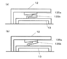
以下、図8を参照しながら、特許文献1に記載されている熱型赤外線センサの構造を説明する。図8(a)は、この赤外線センサの主要部を示す平面図、図8(b)は、図8(a)の8b−8b線断面図である。
Hereinafter, the structure of the thermal infrared sensor described in Patent Document 1 will be described with reference to FIG. FIG. 8A is a plan view showing the main part of the infrared sensor, and FIG. 8B is a cross-sectional view taken along the
図示される赤外線センサは、シリコンなどから形成された基板240と、基板240に支持される受光部241とを備えている。受光部241は、電気抵抗値が温度依存性を有するボロメータ242と、ボロメータ242の電気抵抗値を測定するための配線243とを含んでおり、赤外線センサの感熱部として機能する。配線243は例えばアルミニウムなどの金属から形成されている。
The illustrated infrared sensor includes a
ボロメータ242に対向基板240の上面には、受光部241との間に隙間を形成するように凹部が形成されている。このような凹部は、ウェットエッチングやドライエッチングによって基板240の所定領域を選択的に除去することにより形成される。
A concave portion is formed on the upper surface of the
受光部241は、接触部分245で基板240と接触している。接触部分245の上方には、配線243の両端部244が延びており、不図示の読み出し回路に接続される。
The
以下、図8に示す赤外線センサの動作を説明する。 Hereinafter, the operation of the infrared sensor shown in FIG. 8 will be described.
受光部241が赤外線を吸収すると、ボロメータ242の温度が上昇する。温度上昇により、ボロメータ242の抵抗値が変化する。このとき、配線243を通じてボロメータ242に電流を供給し、抵抗変化によって生じる電圧の変化を検知する。この電圧変化に基づいて、受光部241に入射した赤外線のエネルギを算出することができる。
When the
受光部241は、赤外線の照射によって発生した熱エネルギを外部に逃がさない構造を有していることが好ましい。図示されている例では、受光部241の本体と基板240との間の接触面積を極力低減し、断熱性を向上させている。また、配線243の両端部分244が形成されている部分は、受光部241の本体部分から細長く延びており、基板240に対する熱の伝播を抑制している。以上のように特許文献1の方法では、受光部241と基板240との間の接続部分の形状をできるだけ細長い形状にすることにより、受光部241と基板240との間の断熱特性を向上している。その結果、赤外線の照射による受光部の温度変化が大きくなり、赤外線検出を行うための信号量を大きくすることができる。
It is preferable that the
赤外線センサの断熱構造の他の一例が特許文献2に開示されている。 Another example of the heat insulating structure of the infrared sensor is disclosed in Patent Document 2.
以下、図9を参照しながら、特許文献2に記載されている熱型赤外線センサの構造を説明する。 Hereinafter, the structure of the thermal infrared sensor described in Patent Document 2 will be described with reference to FIG.
図9の赤外線センサは、下部基板110と、上部基板(受光部)120と、ポスト210と、下部電極220と、反射層230と、信号脚200とを備えている。上部基板120にはボロメータ(不図示)が設けられている。
The infrared sensor of FIG. 9 includes a
上部基板120が赤外線を吸収すると、そのボロメータの温度が上昇するため、ボロメータの抵抗値が変化する。このとき、金属層を含む信号脚200を通じてボロメータ82に電流を供給し、抵抗変化によって生じる電圧の変化を検知する。この電圧変化に基づいて、上部基板120に入射した赤外線のエネルギを算出することができる。
When the
ポスト210は、絶縁体から形成されており、上部基板120を下部基板110上に支持する機能を発揮する。下部基板110と上部基板120との間には空洞またはギャップが形成されており、両者の間を断熱している。下部電極220は、信号脚200との間に静電気力を発生して、信号脚200の位置を変化させる。このことにより、信号脚200と上部基板120とは、相互に接触した状態と、非接触の状態とを交互に繰り返すことができる。
The
信号脚200と上部基板120とが非接触の状態にあるときには、上部基板120と下部基板110とは絶縁体のポスト210のみによって接続されているため、上部基板120と下部基板110との間の断熱性が向上する。したがって、赤外線照射による上部基板120の温度上昇を大きくすることができる。非接触状態がある一定時間経過した後、信号脚200と上部基板120とを接触させることにより、ボロメータに電流を供給し、上部基板120に入射した赤外線量を検出する。
When the
上記の赤外線センサでは、赤外線照射による受光部の温度変化が大きくなるため、ボロメータの抵抗変化量、すなわち赤外線検出を行うための信号量を大きくすることができる。 In the above infrared sensor, since the temperature change of the light receiving unit due to infrared irradiation becomes large, the resistance change amount of the bolometer, that is, the signal amount for performing infrared detection can be increased.
このように赤外線センサでは、断熱性を高めることにより、赤外線照射による温度変化量が大きくなり、赤外線検出感度を向上させることが求められている。
上述したように、従来技術においては、受光部と基板との間の接続部分の形状をできるだけ細長い形状にすること、あるいは、受光部と基板との間の接続部分において接触・非接触の状態変化を繰り返すことにより、受光部と基板との間の断熱特性を向上している。このことにより、赤外線照射の有無による受光部の温度変化を大きくし、赤外線検出のための信号量を大きくしている。 As described above, in the prior art, the shape of the connection portion between the light receiving unit and the substrate is made as long as possible, or the contact / non-contact state change in the connection portion between the light receiving unit and the substrate. By repeating the above, the heat insulating property between the light receiving portion and the substrate is improved. As a result, the temperature change of the light receiving portion due to the presence or absence of infrared irradiation is increased, and the amount of signal for infrared detection is increased.
しかしながら、受光部と基板との間の接続部分をできるだけ細長い形状にすることによって断熱特性を向上する場合でも、この受光部と基板との間の接続部分には、熱伝導度の高い金属材料から形成された配線が存在している。そのため、断熱特性をさらに向上させるためには、この配線部をさらに細くする必要がある。しかし、配線部を細くすると、配線部の電気抵抗が高くなる。そのため、電気抵抗に起因して発生する熱ノイズが大きくなり、赤外線を検出するときのSN比が低下するという問題が生じる。 However, even when the heat insulation characteristics are improved by making the connection portion between the light receiving portion and the substrate as long as possible, the connection portion between the light receiving portion and the substrate is made of a metal material having high thermal conductivity. The formed wiring exists. Therefore, in order to further improve the heat insulation characteristics, it is necessary to make this wiring portion thinner. However, if the wiring part is made thinner, the electrical resistance of the wiring part becomes higher. Therefore, the thermal noise generated due to the electrical resistance is increased, and there is a problem that the SN ratio when detecting infrared rays is reduced.
また、接続部分を過度に細長くした場合には、受光部を支持するために必要な剛性を確保できず、破壊が生じるという問題も発生する。 In addition, when the connecting portion is excessively elongated, the rigidity necessary for supporting the light receiving portion cannot be ensured, resulting in a problem of destruction.
これらのことから、受光部と基板との間の接続部分をできるだけ細長い形状にすることによって断熱特性を向上する方法においては赤外線検出のSNを向上するのに限界がある。 For these reasons, there is a limit to improving the SN of infrared detection in the method of improving the heat insulation characteristics by making the connecting portion between the light receiving portion and the substrate as long as possible.
また、受光部と基板との間の接続部分において接触・非接触の状態変化を繰り返すことによって、受光部と基板との間の断熱特性を向上する場合、接触部分の電気抵抗が高くなるため、この部分で発生する熱ノイズが大きくなる。また、接触・非接触を繰り返す接続部分で抵抗値が変化するため、電気信号にノイズが発生することもある。これらの理由から、赤外線検出のSN比を充分に改善することができなくなる。 In addition, by repeating the contact / non-contact state change at the connection part between the light receiving part and the substrate, when the heat insulation characteristics between the light receiving part and the substrate are improved, the electrical resistance of the contact part becomes high, Thermal noise generated in this part becomes large. In addition, since the resistance value changes at the connection portion where contact and non-contact are repeated, noise may occur in the electrical signal. For these reasons, the S / N ratio for infrared detection cannot be sufficiently improved.
なお、一般的な電子デバイスにおいて接触抵抗を低減する方法は、例えば特許文献3などで提案されているが、この場合、例えば接触力を大きくすることが必要である。しかし、このような方法によれば、接触力を過剰に大きくした場合、機械的な破壊が生じるなどの問題が生じるために、ノイズを十分に減少することはできない。
In addition, although the method of reducing contact resistance in a general electronic device is proposed by
本発明は、上記課題を解決するためになされたものであり、その目的とするところは、断熱特性が高く、かつ、ノイズが小さい(SNが高い)電子デバイスを提供することにある。 The present invention has been made to solve the above-described problems, and an object of the present invention is to provide an electronic device having high heat insulation characteristics and low noise (high SN).
本発明の電子デバイスは、赤外線の照射により昇温する少なくとも1つの赤外線吸収部と、温度変化に応じて物理特性が変化する少なくとも1つの感熱部と、前記感熱部の物理特性の変化を検出する検出回路部と、前記赤外線吸収部と前記感熱部とが接触した第1状態と、前記赤外線吸収部と前記感熱部とが離間した第2状態とを交互に切り替えることができる駆動部とを備えている。 An electronic device according to the present invention detects at least one infrared absorbing portion that rises in temperature when irradiated with infrared rays, at least one heat-sensitive portion whose physical characteristics change according to a temperature change, and a change in physical properties of the heat-sensitive portion. A detection circuit unit; and a driving unit capable of alternately switching between a first state in which the infrared absorption unit and the heat sensitive unit are in contact with each other and a second state in which the infrared absorption unit and the heat sensitive unit are separated from each other. ing.
好ましい実施形態において、前記赤外線吸収部は、前記感熱部を覆っている。 In a preferred embodiment, the infrared absorbing portion covers the heat sensitive portion.
好ましい実施形態において、前記検出回路部が形成された基板を備え、前記赤外線吸収部は、絶縁体または半導体からなる吸収部支持体によって前記基板に支持されている。 In a preferred embodiment, the apparatus includes a substrate on which the detection circuit unit is formed, and the infrared absorption unit is supported on the substrate by an absorption unit support made of an insulator or a semiconductor.
好ましい実施形態において、前記赤外線吸収部は、絶縁体または半導体からなる吸収部支持体によって前記感熱部に支持されている。 In a preferred embodiment, the infrared absorbing portion is supported on the heat sensitive portion by an absorbing portion support made of an insulator or a semiconductor.
好ましい実施形態において、前記感熱部と前記検出回路部とは電気的に接続されており、前記赤外線吸収部と前記検出回路部とは配線によって相互に接続されていない。 In a preferred embodiment, the heat sensitive part and the detection circuit part are electrically connected, and the infrared absorption part and the detection circuit part are not mutually connected by wiring.
好ましい実施形態において、前記赤外線吸収部は、電荷を蓄える複数の上部電極を有しており、前記感熱部は、前記上部電極とは逆の極性の電荷を蓄える複数の下部電極を前記上部電極に対向する位置に有しており、前記複数の上部電極は互いに電気的に接続されている。 In a preferred embodiment, the infrared absorbing portion has a plurality of upper electrodes that store charges, and the heat sensitive portion has a plurality of lower electrodes that store charges having a polarity opposite to that of the upper electrodes. The plurality of upper electrodes are electrically connected to each other.
好ましい実施形態において、前記赤外線吸収部及び感熱部の少なくとも一方は、他方に向かって突出する熱接触部を備えている。 In a preferred embodiment, at least one of the infrared absorbing part and the heat sensitive part includes a thermal contact part protruding toward the other.
好ましい実施形態において、前記駆動部は、前記熱接触部の少なくとも一部を変形または移動させることにより、前記第1状態と前記第2状態とを交互に切り替える。 In a preferred embodiment, the driving unit alternately switches between the first state and the second state by deforming or moving at least a part of the thermal contact unit.
好ましい実施形態において、前記駆動部は、前記感熱部及び前記赤外線吸収部の少なくとも一部を変形または移動させることにより、前記第1状態と前記第2状態とを交互に切り替える。 In a preferred embodiment, the driving unit alternately switches between the first state and the second state by deforming or moving at least a part of the heat sensitive unit and the infrared absorbing unit.
好ましい実施形態において、前記検出回路部は、前記物理特性の変化に基づいて前記赤外線の照射量を検知する。 In a preferred embodiment, the detection circuit unit detects an irradiation amount of the infrared rays based on a change in the physical characteristics.
本発明による電子デバイスの制御方法は、赤外線の照射により昇温する赤外線吸収部と、温度変化に応じて物理特性が変化する少なくとも1つの感熱部と、前記感熱部の物理特性の変化を検出する検出回路部と、前記赤外線吸収部と前記感熱部とが接触した第1状態と、前記赤外線吸収部と前記感熱部とが離間した第2状態とを交互に切り替えることができる駆動部とを備えた電子デバイスの制御方法であって、前記赤外線吸収部に対して赤外線を照射するステップと、前記赤外線吸収部と前記感熱部とが接触した第1状態で前記感熱部の温度を測定するステップとを含む。 The method for controlling an electronic device according to the present invention detects an infrared absorbing portion that rises in temperature when irradiated with infrared rays, at least one heat-sensitive portion whose physical characteristics change according to a temperature change, and a change in physical properties of the heat-sensitive portion. A detection circuit unit; and a driving unit capable of alternately switching between a first state in which the infrared absorption unit and the heat sensitive unit are in contact with each other and a second state in which the infrared absorption unit and the heat sensitive unit are separated from each other. A method of controlling the electronic device, the step of irradiating the infrared ray absorbing portion with infrared rays, and the step of measuring the temperature of the heat sensitive portion in a first state where the infrared ray absorbing portion and the heat sensitive portion are in contact with each other. including.
好ましい実施形態において、前記赤外線吸収部に対して赤外線を照射するステップは、前記赤外線吸収部と前記感熱部とが離間した第2状態で実行する。 In a preferred embodiment, the step of irradiating the infrared ray absorbing portion with infrared rays is performed in a second state in which the infrared ray absorbing portion and the heat sensitive portion are separated from each other.
好ましい実施形態において、前記赤外線吸収部と前記感熱部とが接触した第1状態で前記感熱部の温度を測定するステップを実行した後、前記第1状態で熱の少なくとも一部を外部に逃すステップを行う。 In a preferred embodiment, after performing the step of measuring the temperature of the heat-sensitive part in a first state where the infrared absorption part and the heat-sensitive part are in contact, at least part of the heat is released to the outside in the first state. I do.
好ましい実施形態において、前記赤外線吸収部に対して赤外線を照射するステップは、前記赤外線吸収部と前記感熱部とが接触した第1状態、および前記赤外線吸収部と前記感熱部とが離間した第2状態のいずれか一方を選択し、その選択された状態で実行する。 In a preferred embodiment, the step of irradiating the infrared ray absorbing portion with infrared rays includes a first state in which the infrared ray absorbing portion and the heat sensitive portion are in contact with each other, and a second state in which the infrared ray absorbing portion and the heat sensitive portion are separated from each other. Select one of the states and execute in the selected state.
本発明の電子デバイスでは、読出しを行うとき以外のときには、感熱部と赤外線吸収部とが空間的に離れた状態で主に赤外線吸収部に熱が蓄えられるため、熱を蓄える部分から外部への熱の逃げを最小限に抑制することができる。しかも、感熱部と検出回路部とを接続する配線は接続したままにすることができるため、配線の接触・非接触を繰り返すことに起因するノイズも発生しない。このように、本発明によれば、熱を蓄える部分と外部との間の断熱性が向上するため、赤外線の入射量に対応して温度が大きく変化し、かつ、接触抵抗によるノイズも問題にならないため、赤外線検出のSNを向上させ、赤外線入射量の検出を高い精度で実行することができる。 In the electronic device of the present invention, since heat is stored mainly in the infrared absorbing part in a state where the heat sensitive part and the infrared absorbing part are spatially separated at times other than when reading is performed, from the part storing the heat to the outside Heat escape can be minimized. In addition, since the wiring connecting the heat-sensitive part and the detection circuit part can be kept connected, noise caused by repeated contact / non-contact of the wiring does not occur. As described above, according to the present invention, since the heat insulation between the heat storage portion and the outside is improved, the temperature greatly changes in response to the amount of incident infrared rays, and noise due to contact resistance is also a problem. Therefore, the SN of infrared detection can be improved, and the detection of the infrared incident amount can be performed with high accuracy.
(実施形態1)
以下、図面を参照しながら、本発明による電子デバイスの第1の実施形態を説明する。本実施形態の電子デバイスは、抵抗変化型の赤外線センサであるが、本発明はこれに限定されず、焦電型赤外線センサやサーモパイル型赤外線センサや誘電ボロメータ型赤外線センサなどの他のタイプの電子デバイスにも適用可能である。
(Embodiment 1)
Hereinafter, a first embodiment of an electronic device according to the present invention will be described with reference to the drawings. The electronic device of the present embodiment is a resistance change type infrared sensor, but the present invention is not limited to this, and other types of electronic devices such as a pyroelectric infrared sensor, a thermopile infrared sensor, and a dielectric bolometer type infrared sensor. It can also be applied to devices.
本明細書では、赤外線センサのうち、温度変化に応じて物理特性が変化し、その変化に基づいて赤外線照射量が検出される部分を「赤外線検出部」と称することにする。たとえば、抵抗変化型の赤外線センサにおいては、抵抗変化材料からなるボロメータが赤外線検出部である。本発明における「感熱部」とは、このような赤外線検出部を含み、赤外線検出部とともに一体的に移動・変形する部材である。なお、本明細書における「物理特性」とは、典型的には、電気抵抗、電荷量、電流値、電圧値、および誘電率を含む。 In the present specification, a portion of the infrared sensor in which physical characteristics change according to a temperature change and an infrared irradiation amount is detected based on the change is referred to as an “infrared detector”. For example, in a resistance change type infrared sensor, a bolometer made of a resistance change material is an infrared detector. The “heat sensitive part” in the present invention is a member that includes such an infrared detection part and moves and deforms integrally with the infrared detection part. Note that “physical characteristics” in this specification typically includes electrical resistance, charge amount, current value, voltage value, and dielectric constant.
まず、図1(a)及び(b)を参照して、本実施形態における電子デバイスの概略構成を説明する。図1(a)は、本実施形態の斜視図であり、図1(b)は、図1(a)における1b−1b線を含み基板部11の表面に対して垂直な面で切断した断面図である。
First, a schematic configuration of the electronic device in the present embodiment will be described with reference to FIGS. FIG. 1A is a perspective view of the present embodiment, and FIG. 1B is a cross section taken along a plane perpendicular to the surface of the
本実施形態の電子デバイスは、図1(a)に示されるように、基板部11と、基板部11の上面に支持されたれた赤外線吸収部12及び感熱部13とを備えている。
As shown in FIG. 1A, the electronic device of this embodiment includes a
基板部11は、例えば集積回路が形成された半導体基板であり、不図示の検出回路部を備えている。検出回路部は、感熱部13における赤外線検出部の物理的変化(例えば電気抵抗値の変化)を検知する。赤外線吸収部12は、赤外線吸収部12の全体を支えるための吸収部支持体121に接続されている。吸収部支持体121の一端は常に基板部11に接触し、吸収部支持体121は赤外線吸収部12を基板部11に固定している。赤外線吸収部12の一部または全部は変形可能な弾性を有しており、基板部11に対する位置関係・姿勢が変化し得る。感熱部13は、赤外線吸収部12と基板部11との間に位置しており、赤外線吸収部12によって覆われている。感熱部13の表面のうち、赤外線吸収部12と対向する領域には、赤外線吸収部12に対して突出する熱接触部135が形成されている。
The
赤外線吸収部12及び感熱部13の内部構造の詳細は後述する。
Details of the internal structures of the infrared absorbing
本実施形態の電子デバイスでは、熱接触部135の上端と赤外線吸収部12の下面の一部が「接触」および「非接触」の間で状態遷移を繰り返す。赤外線吸収部12と感熱部12との間の「接触」および「非接触」の状態遷移は、静電気力などを用いて実現することができる。すなわち、静電誘導によって赤外線吸収部12に電荷を発生させて、この電荷に加わる静電気力を用いて吸収部支持体121および赤外線吸収部12の一部または全体を変形させることにより、上記接触及び切断の繰り返しを行うことができる。変形時、赤外線吸収部12は、吸収部支持体121によって基板部11に固定されているため、片持ち梁のように動作する。言い換えると、赤外線吸収部12の自由端側が固定端側を軸として傾斜(チルト)する。図2(a)及び(b)は、それぞれ、接触の状態及び非接触の状態を模式的に示している。図において、赤外線吸収部12の姿勢が変化する例を示しているが、吸収部支持体121が変形して吸収部支持体121と赤外線吸収部12の姿勢が変化する構成を採用しても良い。また、変形する部分は、吸収部支持体121および赤外線吸収部12に含まれるいずれの部分であってもよい。更に、後述するように、感熱部13と感熱部支持体131に含まれるいずれかの部分が変化する構成を採用しても良い。重要な点は、赤外線吸収部12と感熱部13との間で「接触」および「非接触」の状態遷移を行うことである。
In the electronic device of this embodiment, the upper end of the
以下、感熱部13及び赤外線吸収部12の構成を詳しく説明する。
Hereinafter, the structure of the heat
まず、図3(a)から図3(c)を参照しつつ、感熱部13の構成を詳しく説明する。図3(a)は、図1(b)と同じ断面における断面図であり、感熱部13の構成を詳しく示している。図3(b)は、図3(a)の3b−3b線断面図、図3(c)は、図3(a)の3c−3c線断面図である。
First, the configuration of the heat
感熱部13は、ボロメータ132、ボロメータ保護膜133、配線部134a、熱接触部135、第1静電誘導下部電極136、第2静電誘導下部電極137、第1コンタクト部138と、第2コンタクト部139を備えている。感熱部13は、図1(a)に示されている感熱部支持体131によって基板部11に固定されている。
The
図3(b)には、感熱部13におけるボロメータ132の平面レイアウトが示されている。ボロメータ132は、抵抗率の温度依存性が大きな材料(例えばポリシリコン、チタン、酸化バナジウムなど)から形成され、蛇行している。ボロメータ132の両端は、配線部134aに接続されている。ボロメータ保護膜133は、ボロメータ132を保護する機能を持ち、たとえば、シリコン酸化膜などの絶縁材料から形成されており、ボロメータ132を被覆している。
FIG. 3B shows a planar layout of the
感熱部13の温度が変化すると、ボロメータ132の電気抵抗値が変化する。この電気抵抗値の変化は、基板部11に設けられた不図示の「読み出し回路部(検出回路部)」によって検知される。すなわち、読み出し回路によって、ボロメータ132の抵抗値の変化を電気的に検出することにより、感熱部13の温度変化が求められる。
When the temperature of the heat
第1静電誘導下部電極136及び第1コンタクト部138は、電気配線134aに接続されている。同様に、第2静電誘導下部電極137及び第2コンタクト部139も、他の電気配線134aに接続されている。電気配線134aは、図1(a)に示されている感熱部支持体131を通って基板部11の読み出し回路部に接続されている。
The first electrostatic induction
感熱部13の第1静電誘導下部電極136と第2静電誘導下部電極137とは、配線部134bによって相互に接続されている。第1静電誘導下部電極136及び第2静電誘導下部電極137は、それぞれ、第1コンタクト部138及び第2コンタクト部139を介して配線部134aに接続されている。
The first electrostatic induction
次に、図4(a)及び(b)を参照しながら、赤外線吸収部12の構成を説明する。図4(a)は、図3(a)と同一の断面図であり、図4(b)は、図4(a)の4b−4b線を含み基板部11に平行な面で切り取った断面図である。
Next, the configuration of the
赤外線吸収部12は、吸収部支持体121、第1静電誘導上部電極122、第2静電誘導上部電極123、配線部124、及び吸熱部125を備えている。
The
吸熱部125は、例えばSiO2などの材料で形成されており、入射する赤外線を吸収する機能を発揮する。第1静電誘導上部電極122は、感熱部13の第1静電誘導下部電極136に対向する位置に形成されており、これらの第1静電誘導電極122、136は、図5に示す第1のコンデンサ62を形成する。また、第2静電誘導上部電極123は、感熱部13の第2静電誘導下部電極137に対向する位置に形成されており、これらの第2静電誘導電極123、137は、図5に示す第2のコンデンサ63を形成する。
The
図5は、上記各部が形成する電気回路の構成の概要を示す等価回路図である。読出し回路には、電源部61と、電源部61とボロメータ132との間で電気的接続をON−OFFするための電気的スイッチ部60とが含まれている。電気的スイッチ部60は、例えばMOSトランジスタなどから形成される。なお、後述するように、同一の基板部上に複数の赤外線吸収部および感熱部を配置した電子デバイスを形成することも可能である。例えば、赤外線吸収部および感熱部を含む図1に示すような基本構成をセルとして、複数のセルの1次元または2次元的な配列(セルアレイ)を同一基板部上に形成することも可能である。この場合、電源部を全てのセルで共通として、電源部とボロメータとの間の電気的接続のON−OFFをセルごとに独立して行うことも可能である。
FIG. 5 is an equivalent circuit diagram showing an outline of the configuration of the electric circuit formed by each of the above-described parts. The readout circuit includes a
図5(a)は、電気的スイッチ部60がOFFになっている状態を示している。この状態においては、ボロメータ132には電流は流れず、第1のコンデンサ62および第2のコンデンサ63には電荷は蓄積されていない。このため、赤外線吸収部12と感熱部13との間に静電気力は発生せず、赤外線吸収部12と感熱部13とは非接触の状態となる。
FIG. 5A shows a state where the
一方、図5(b)は、電気的スイッチ部60がONになっている状態を示している。この状態においては、ボロメータ132には電流iが流れており、ボロメータ132の両端には電圧V0が印加される。このため、図5(b)に示すように、第1のコンデンサ62および第2のコンデンサ63には電荷Qが蓄積される。この結果、各コンデンサの2個の電極間に静電引力が発生し、赤外線吸収部12と感熱部13は接触する。赤外線吸収部12と感熱部13が接触すると、両者の間で熱のやり取りが行われ、十分短い時間(例えば1ミリ秒〜1マイクロ秒)の後に、両者の温度はほぼ同じになる。このときの赤外線吸収部12と感熱部13の温度は、例えば室温よりも約1℃高い温度である。室温からの約1℃の温度上昇のうち、例えば約0.1℃の温度上昇が被写体からの赤外線入射によるものであり、残りの約0.9℃の温度上昇がジュール熱によるものである。ただし、ここでは、同一基板部上に複数のセルが2次元的に配列された構成のセンサチップとレンズとを備えた赤外線カメラを想定しており、被写体の温度が室温に比べて1℃高い場合を考えた。
On the other hand, FIG. 5B shows a state where the
なお、説明を簡単にするために、ボロメータ132以外の部分での電気抵抗を無視している。電気的スイッチ部60をONの状態からOFFの状態にスイッチングすると、赤外線吸収部12と感熱部13との間の静電気力はなくなるため、赤外線吸収部12および吸収部支持体121の弾性により、赤外線吸収部12と感熱部13とは非接触の状態となる。
In order to simplify the explanation, the electrical resistance in parts other than the
このように本実施形態では、赤外線吸収部12と感熱部13との間の熱的な接触/非接触の切換を行う駆動部として、電極122、123、136、137を利用している。
As described above, in the present embodiment, the
ボロメータ132は温度によって抵抗値が変化する特性を有するため、電気的スイッチ部60がONになっている状態で、ボロメータ132に流れる電流iの大きさ、または、その時間変化を検出することにより、ボロメータ132の温度または温度変化を検出できる。上で説明したように、赤外線吸収部12と感熱部13が接触した状態では、十分短い時間の後に、両者の温度はほぼ同じになるので、この状態におけるボロメータ132の温度を検出することにより、赤外線吸収部12が吸収した赤外線の量を計算することが可能である。
Since the
以下、ボロメータ132の温度から、赤外線吸収部12が吸収した赤外線の量を計算する方法を簡単に説明する。
Hereinafter, a method of calculating the amount of infrared rays absorbed by the infrared absorbing
赤外線吸収部12の熱容量をY1、感熱部13の熱容量をY2とする。また、赤外線が入射していないときのボロメータ132の温度をT0、赤外線が入射したときのボロメータ132の温度をT1とする。更に、赤外線吸収部12が赤外線を吸収することによって発生する熱をN0、赤外線吸収部12から感熱部13以外の部分に逃げる熱量をN1、感熱部13から赤外線吸収部12以外の部分に逃げる熱量をN2とする。このとき、赤外線吸収部12と感熱部13とを組み合わせた系と外部との熱のやりとりを考えると、以下の関係が成立する。
N0−N1−N2=(Y1+Y2)×(T1−T0)
ここで、熱量N1は、赤外線吸収部12と、感熱部13以外の部分との間の熱コンダクタンスなどから計算することができる。また、熱量N2は、感熱部13と、赤外線吸収部12以外の部分との間の熱コンダクタンスなどから計算することができる。なお、上記の説明では、説明を簡単にするため、電流によるジュール熱を無視している。
The heat capacity of the
N0-N1-N2 = (Y1 + Y2) × (T1-T0)
Here, the amount of heat N1 can be calculated from the thermal conductance between the infrared absorbing
また、赤外線吸収部に吸収されずに、感熱部に直接入射した赤外線によって発生した熱も考慮して、赤外線の照射量を検出することで、より詳細な検出が可能となる。 In addition, more detailed detection is possible by detecting the irradiation amount of infrared rays in consideration of heat generated by infrared rays directly incident on the heat-sensitive portion without being absorbed by the infrared absorption portion.
本実施形態では、吸収部支持体121が熱伝導度の低い断熱材料から形成されているため、熱量N1は、従来の赤外線センサに比べて小さくすることができる。また、読出し時間を短くすることにより、熱量N2を、従来の赤外線センサにおいて対応する熱量に比べて小さくすることもできる。例えば、熱量N1およびN2の大きさを、それぞれ、従来例の数値に比べて約1/10に低減することができる。その結果、従来、赤外線入射による感熱部の温度上昇が例えば約0.01℃であったのに対し、本発明では例えば約0.1℃に増加させることが可能になる。ただし、この温度上昇の数値例は、同一基板部上に複数のセルが2次元的に配列された構成のセンサチップとレンズとを備えた赤外線カメラを想定して計算したものであり、被写体の温度が室温に比べて1℃高い場合を考えている。また、ジュール熱は無視している。
In this embodiment, since the absorption
これらの理由から、本実施形態におけるボロメータ132の温度変化(T1−T0)は、従来技術において対応する温度変化に比べて大きくなる。このため、本実施形態の赤外線センサは従来技術の赤外線センサに比べて高感度である。
For these reasons, the temperature change (T1-T0) of the
図5の回路構成を用いれば、ボロメータ132に電流を供給して抵抗変化を検出するための配線と、第1静電誘導下部電極136および第2静電誘導下部電極137に電圧を印加するための配線が共用されているので、これらを別々の配線で形成した場合に比べて配線を通した熱コンダクタンスを小さくすることができる。このため、感熱部13の断熱特性を向上でき、赤外線検出感度を向上できる。さらに、赤外線吸収部12と感熱部13との間、および、赤外線吸収部12と基板部11との間に配線がないため、赤外線吸収部12と感熱部13との間の断熱特性、および、赤外線吸収部12と基板部11との間の断熱特性が向上し、赤外線検出感度が向上する。
If the circuit configuration of FIG. 5 is used, a voltage is applied to the wiring for supplying a current to the
本実施形態では、赤外線吸収部12と感熱部13との間で接触・非接触の状態を交互に切り換えるため、駆動部によって赤外線吸収部12の一部分を変形させ、赤外線吸収部12の一部分と感熱部13の一部分との位置関係を変化させている。しかし、本発明は、このような場合に限定されず、駆動部によって赤外線吸収部12の全部分を変形させてもよいし、感熱部13の一部または全部を変形させてもよい。また、赤外線吸収部12および感熱部13の全部または一部をともに変形させるようにしてもよい。重要な点は、赤外線吸収部12と感熱部13との間で接触・非接触の状態遷移が繰り返され得ることである。
In the present embodiment, in order to alternately switch the contact / non-contact state between the infrared absorbing
本実施形態では、吸収部支持体121が断熱性の高い絶縁材料(たとえばSiO2)から形成されている。配線材料として通常使用されるアルミニウムの熱伝導度は、およそ1.32W/cm・Kの値であるが、SiO2(酸化シリコン)の熱伝導度は、およそ0.014W/cm・Kである。このため、赤外線吸収部12が感熱部13に対して「非接触」の状態にあるときは、赤外線吸収部121と他の部分との間の断熱性は極めて高い。したがって、赤外線の入射量が変化した場合、赤外線吸収部12の温度が従来技術と比べて大きく変化する。赤外線吸収部121と他の部分との間の断熱性を更に高めるためには、空洞の内部を減圧(例えば50mTorr以下)または真空状態にしてもよい。
In the present embodiment, the absorbing
図示される例では、吸収部支持体121が基板部11の表面に対して垂直方向に伸びる直線の形状を有しているが、赤外線吸収部12と基板部11との間の断熱特性を向上させるために、吸収部支持体121の一部が蛇行しているような形状を採用しても良い。
In the illustrated example, the
上記のように、本実施形態では、赤外線吸収部12が感熱部13に対して常に「非接触」の状態にあるのではなく、感熱部13において赤外線検出部として機能する部分の物理特性の変化を検知する必要があるとき、赤外線吸収部12と感熱部13を「接触」させる。この接触により、赤外線吸収部12と感熱部13が熱的に接触する。
As described above, in the present embodiment, the
熱接触部135の高さは例えば約1μmであり、断面積は例えば100μm2である。熱接触部135は例えばアルミニウムなどの金属から形成されており、熱接触部135の両端間の熱コンダクタンスは大きい。このため、赤外線吸収部12と感熱部13を「接触」させた場合、きわめて短い時間で赤外線吸収部12と感熱部13の温度がほぼ同じになる。この状態で感熱部13の温度を検出回路部によって検出することにより、赤外線の入射量またはその変化量を検出することが可能になる。
The height of the
本実施形態では、赤外線吸収部12と感熱部13との間で「接触」および「非接触」の状態遷移を行う。このことにより、赤外線吸収部12と感熱部13とが熱的に接触する状態と、熱的に接触しない状態を繰り返すことが可能になる。すなわち、赤外線吸収部12と感熱部13との位置関係を変化させることにより、赤外線吸収部12と感熱部13とが、いわば「熱的スイッチ」を形成する。2個の物体間の位置関係を変化させることによって形成される他のスイッチとして、両者が接触の状態にあるときに電気的に接続して、両者が非接触の状態にあるときに電気的に切断する「電気的スイッチ」がある。「電気的スイッチ」を有する電子デバイスにおいては、一般的に接触部分の電気抵抗がノイズとなって、センサに用いる場合にはその感度が低下するという問題がある。しかし、本実施形態においては、赤外線吸収部12と感熱部13とによって形成されるスイッチは、電気的スイッチでないため、接触部分の電気抵抗によるノイズ発生の問題はない。
In the present embodiment, the state transition of “contact” and “non-contact” is performed between the infrared absorbing
なお、本実施形態では、赤外線吸収部12と感熱部13とが接触した状態で、感熱部13の温度を検出回路部によって検出しているが、本発明はこの場合に限定されない。赤外線吸収部12と感熱部13とを接触させた後、赤外線吸収部12と感熱部13とを非接触の状態にし、その状態において感熱部13の温度を検出回路部によって検出してもよい。また、赤外線吸収部12と感熱部13とを接触させた後、一定時間が経過してから感熱部13の温度を検出回路部によって検出してもよい。
In the present embodiment, the temperature of the heat
感熱部13は、図1において単純化され、単に平板なプレートであるかのように記載されているが、現実の構成は、後に詳しく説明するように赤外線検出素子として機能するボロメータなどを備えている。
Although the heat-
感熱部13の形状は、数mm×数mmの矩形範囲に収まる平面サイズを有していることが好ましく、例えば30μm×30μmの矩形形状を有している。感熱部13の厚さは、例えば1mm以下であり、本実施形態では2μm程度に設定されている。静電気力などの非接触力によって感熱部13の位置を高速で移動させるには、感熱部13を小型化し、その質量を低減することが望ましい。なお、感熱部13を小型化することは、感熱部13の熱容量を低減する効果ももたらす。
The shape of the heat-
例えば、厚さ2μm、縦30μm×横30μmの薄板形状を有する小型の感熱部13を用いる場合でも、適当なレンズを使用することにより、十分な量の赤外線を上方から感熱部13に入射させることができる。赤外線吸収部12と感熱部13が非接触の状態にあるときの両者の距離は、0.5〜5μmの範囲内の値、例えば2μm程度に設定され得る。この程度の隙間が形成されると、赤外線吸収部12と感熱部13が非接触の状態にあるときに、赤外線吸収部12と感熱部13との間は十分に断熱されるため、赤外線検出感度が向上する。
For example, even when a small heat-
図6は、同一の基板部11上に複数の赤外線吸収部12および感熱部13を配置した電子デバイスの断面を模式的に示している。図6に示す例では、図1に示すような基本構成を1つのセルとし、複数のセルの1次元または二次元的な配列(セルアレイ)を同一基板部11上に形成している。このようなセルアレイを有することにより、赤外線のラインセンサまたはイメージセンサを構成することができる。基板部11上には、トランジスタなどの回路素子を構成要素として含む周辺回路が形成されている。この周辺回路は、検出回路部(データ読み出し回路)や赤外線吸収部12の位置の駆動を制御する駆動回路などを含んでいる。感熱部13と周辺回路との電気的接続は、図3に示す配線部134aを含む電気配線(図6において不図示)によって接続されている。
FIG. 6 schematically shows a cross section of an electronic device in which a plurality of infrared absorbing
上記のセルが行および列からなるマトリクス状に配列されている場合、周辺回路は、行または列単位でセルからデータの読み出しを行う。例えば、行単位でデータの読み出しをおこなう場合、N行目(Nは自然数)のセルアレイからデータの逐次読み出しを行った後、N+1行目のセルアレイから同様にデータの逐次読み出しを行う。この動作を繰り返すことにより、2次元的な配列されたセルアレイからのデータを得て、赤外線のイメージを形成することができる。 When the cells are arranged in a matrix composed of rows and columns, the peripheral circuit reads data from the cells in units of rows or columns. For example, when data is read in units of rows, data is sequentially read from the cell array of the Nth row (N is a natural number), and then the data is sequentially read from the cell array of the (N + 1) th row. By repeating this operation, data from a two-dimensional array of cell arrays can be obtained and an infrared image can be formed.
同一基板部11上に複数のセルが行および列状に配列された実施形態において、個々のセルが有するボロメータ21の電気抵抗値の変化を、上記の方法で順番に検出すれば、各セルにおける赤外線入射強度の面内分布を高感度に検知することができるため、高感度な赤外線のイメージを得ることができる。
In the embodiment in which a plurality of cells are arranged in rows and columns on the
なお、本実施形態では、赤外線吸収部12と感熱部13との間の「接触」および「非接触」の状態遷移を、静電誘導による静電気力を用いて行っているが、静電誘導による静電気力の代わりに、たとえば、エレクトレットコンデンサの電極間の静電気力を用いてもよい。また、強誘電体と電極との間の静電気力を用いて実現することも可能である。エレクトレットコンデンサの電極は、内部に電荷を蓄積しているので、電極間に電圧を加えてもう一方の電極に電荷を発生させることによって、電極間に静電気力を発生させることができる。あるいは、静電気力を用いる代わりに電磁力を用いてもよい。たとえば、赤外線吸収部12に強磁性体からなる部分を形成するとともに、感熱部13にコイルを形成すれば、コイルに電流を流したとき、強磁性体とコイルとの間に電磁力を発生させることができる。この電磁力を用いることによって赤外線吸収部12と感熱部13との位置関係を変化させれば、両者の間で「接触」および「非接触」の状態遷移を行うことも可能である。
In the present embodiment, the “contact” and “non-contact” state transition between the infrared absorbing
本実施形態では、赤外線吸収部12の一端が固定されて赤外線吸収部12が片もち梁のように変形するため、動作の安定性がよく、赤外線吸収部12における変形部分の位置の制御を簡単に行うことが可能である。これに対して、赤外線吸収部12を他の部分と完全に切断された形状で形成することも可能である。すなわち、赤外線吸収部12と感熱部13が非接触の状態にあるときに、赤外線吸収部12が外部と接触することなく浮上するような構成をとることも可能である。この構成によれば、赤外線吸収部12と感熱部13とが「非接触」の状態にあるときに、赤外線吸収部12と他の部分との断熱特性がさらに向上するために、感度をさらに向上することができる。
In the present embodiment, one end of the
なお、赤外線吸収部12が他の部分から完全に切断された形状である場合、赤外線吸収部12の表面に複数の電極を形成して、それらの電極と対向する位置にも電極を形成して、対向する電極間で形成されるコンデンサに蓄えられている電荷の時間変化を検出することなどにより、赤外線吸収部12の位置を検出することができる。そして、この位置情報をフィードバックすれば、赤外線吸収部12と感熱部13との間の静電気力の大きさを制御することにより、赤外線吸収部12の位置を精密に制御することが可能である。このことにより、赤外線吸収部12と感熱部13との両者の「接触」および「非接触」の状態遷移を行うことが可能である。
In addition, when the
熱接触部135の上面の面積を大きくすれば、赤外線吸収部12と感熱部13との間の熱のやりとりが更にスムーズに行われるため、読出し時間を短縮することが可能である。また、熱接触部135の上面に傾きを設け、赤外線吸収部12と感熱部13とが接触状態にあるときに両者の密着性を向上させれば、赤外線吸収部12と感熱部13との間の熱のやりとりが更にスムーズに行われるため、読出し時間を短縮することが可能である。
If the area of the upper surface of the
上記の実施形態では、赤外線吸収部12の少なくとも一部が基板部11の表面に対して垂直な方向に変位しているが、この変位の方向は、基板部11の表面に平行であってもよい。その場合、熱接触部135は、基板部11の表面に平行な方向に突出することが好ましい。
In the above embodiment, at least a part of the infrared absorbing
上記の実施形態では、赤外線吸収部12と基板部11とが直接に接続されているが、本発明は、このような場合に限定されない。図7に示すように、赤外線吸収部12が感熱部13に支持されている構成を採用しても良い。この場合、赤外線吸収部12と感熱部13との間の接続部分を長くするか、あるいは、接続部分を蛇行させることにより、赤外線吸収部12と感熱部13との間の熱コンダクタンスを小さくすることができる。
In the above embodiment, the infrared absorbing
上記の実施形態では、感熱部13に電極を設けて赤外線吸収部12の位置を変化させているが、基板部11に電極を設け、赤外線吸収部12の位置を変化させるようにしてもよい。また、感熱部13の位置を変化させることによって、赤外線吸収部12と感熱部13との間で接触・非接触の状態変化をさせる構成を採用することもできる。
In the above embodiment, an electrode is provided in the heat
なお、感熱部13の温度を検出回路部によって検出した後、赤外線吸収部12と感熱部13とを接触させた状態で、ある一定時間保持し、赤外線吸収部12および感熱部13の温度をリセットしてもよい。この場合、温度のリセット後に、赤外線吸収部12と感熱部13とを非接触の状態にし、赤外線吸収を行うことになる。この方法によれば、温度がリセットされるため、感熱部13の温度を検出回路部によって検出した後、その信号が、次に感熱部13の温度を検出回路部によって検出するときの信号に混入することを防止できる。このことにより、赤外線センサの応答時間を短縮することができる。また、上記の方法を用いて赤外線ラインセンサや赤外線イメージセンサを形成すると、得られる赤外線のイメージにおいて残像を減らす効果がある。また、基板と感熱部、または、基板と赤外線吸収部との間に、新たにリセット用の熱スイッチを設けて、感熱部13の温度を検出回路部によって検出した後に、リセット動作を行うことも可能である。この場合、リセット用の熱スイッチにおける熱コンダクタンスを、赤外線吸収部と基板の間の熱コンダクタンスおよび感熱部と基板の間の熱コンダクタンスよりも大きくすることが可能であるので、リセット動作をより効率的に短時間で行うことが可能である。
In addition, after the temperature of the heat
基板部11または感熱部13に反射板を設け、赤外線吸収部12を透過した赤外線を反射して、再び赤外線吸収部12に入射させてもよい。そうすることにより、赤外線吸収部12における赤外線吸収率を向上させ、赤外線検出感度を向上することが可能になる。
A reflection plate may be provided on the
以下、本発明による電子デバイスの好ましい制御方法を説明する。 Hereinafter, a preferred method for controlling an electronic device according to the present invention will be described.
まず、熱型赤外線センサにおける感度と応答時間の関係について説明する。 First, the relationship between sensitivity and response time in a thermal infrared sensor will be described.
一般的な熱型赤外線センサでは、熱を蓄える部分と外部との間の熱コンダクタンスが小さいほど、感度が大きくなるが、応答時間が遅くなる。本発明による電子デバイスの好適な実施形態である赤外線センサでは、赤外線吸収部と感熱部とが非接触の状態において、主に赤外線吸収部に熱が蓄えられる。また、赤外線吸収部と感熱部とが接触している状態においては、赤外線吸収部に蓄えられた熱が感熱部にも移動し、主に赤外線吸収部と感熱部に熱が蓄えられる。 In a general thermal infrared sensor, the smaller the thermal conductance between the heat storage portion and the outside, the greater the sensitivity but the slower the response time. In the infrared sensor which is a preferred embodiment of the electronic device according to the present invention, heat is mainly stored in the infrared absorption section in a state where the infrared absorption section and the heat sensitive section are not in contact with each other. Further, in a state where the infrared absorbing portion and the heat sensitive portion are in contact, the heat stored in the infrared absorbing portion moves to the heat sensitive portion, and heat is mainly stored in the infrared absorbing portion and the heat sensitive portion.
したがって、赤外線吸収部と感熱部とが非接触の状態においては、熱を蓄える部分と外部との間の熱コンダクタンスが吸収部支持体の熱コンダクタンスにほぼ等しくなる。一方、赤外線吸収部と感熱部とが接触している状態においては、熱を蓄える部分と外部との間の熱コンダクタンスが、感熱部支持体の熱コンダクタンスと吸収部支持体の熱コンダクタンスの和にほぼ等しくなる。 Therefore, in a state where the infrared absorbing portion and the heat sensitive portion are not in contact with each other, the thermal conductance between the heat storing portion and the outside is substantially equal to the thermal conductance of the absorbing portion support. On the other hand, in the state where the infrared absorption part and the heat sensitive part are in contact, the thermal conductance between the heat storage part and the outside is the sum of the thermal conductance of the heat sensitive part support and the heat conductance of the absorption part support. Almost equal.
なお、熱を蓄える部分と外部との間の熱コンダクタンスをより正確に求めるには、熱を蓄える部分から対流および輻射などによって外部に逃げる熱を考慮する必要がある。 In order to more accurately determine the thermal conductance between the heat storage portion and the outside, it is necessary to consider the heat that escapes from the heat storage portion by convection and radiation.
熱型赤外線センサの熱を蓄える部分の温度変化は、一般的に、以下の微分方程式によって示される。
C×dT/dt =QA −g×(T−Ts)
ここで、Cは熱を蓄える部分の熱容量、Tは熱を蓄える部分の温度、tは時間、dT/dtはTのtに対する微分値、QAは単位時間当たり熱を蓄える部分が吸収する熱量、gは熱を蓄える部分と外部との間の熱コンダクタンス、Tsは外部の温度である。簡単のために、ジュール熱などの効果を無視している。
In general, the temperature change of the portion that stores heat of the thermal infrared sensor is represented by the following differential equation.
C × dT / dt = Q A −g × (T−Ts)
Here, C is the heat capacity of the part that stores heat, T is the temperature of the part that stores heat, t is time, dT / dt is the differential value of T with respect to t, and Q A is the amount of heat absorbed by the part that stores heat per unit time. , G is the thermal conductance between the heat storage portion and the outside, and Ts is the outside temperature. For simplicity, effects such as Joule heat are ignored.
上記の微分方程式によれば、QAが一定であるとき、Tは初期値から指数関数的に変化し、その収束値はTs+QA/gに等しく、その時定数τはC/gに等しい。ここでは、QAが一定である場合を想定したが、この状況は、例えば位置と温度が一定の被写体から輻射で発生する赤外線を固定位置の赤外線センサで検出する場合などに相当する。また、簡単のためにgが一定であると仮定したが、実際には本発明の赤外線センサにおいては、上で説明したように、赤外線吸収部と感熱部が接触・非接触の状態変化を行うために、gの値は変化する。しかしながら、いずれにせよ各時刻におけるgの値が小さいほど、Tの収束値が大きく、赤外線センサの感度が大きくなることがわかる。また各時刻におけるgの値が小さいほど、時定数τが大きいので、Tが収束するまでの時間が長くなる。すなわち、応答時間が長くなる。 According to the above differential equation, when Q A is constant, T changes exponentially from the initial value, its convergence value is equal to Ts + Q A / g, and its time constant τ is equal to C / g. . Here, it is assumed that Q A is constant, but this situation corresponds to, for example, a case where infrared rays generated by radiation from a subject having a fixed position and temperature are detected by an infrared sensor at a fixed position. For simplicity, it is assumed that g is constant. However, in the infrared sensor according to the present invention, as described above, the infrared absorption part and the heat sensitive part change in a contact / non-contact state. Therefore, the value of g changes. However, in any case, it can be seen that the smaller the value of g at each time, the greater the convergence value of T and the greater the sensitivity of the infrared sensor. Also, the smaller the value of g at each time, the longer the time constant τ, and the longer the time until T converges. That is, the response time becomes long.
以上の説明から明らかなように、一般的な熱型赤外線センサでは、熱を蓄える部分と外部との間の熱コンダクタンスが小さいほど感度が大きくなるが、応答時間が増加する(応答性が悪くなる)という関係がある。 As is apparent from the above description, in a general thermal infrared sensor, the sensitivity increases as the thermal conductance between the heat storage part and the outside decreases, but the response time increases (the responsiveness deteriorates). )
なお、一般的な赤外線センサにおいて、gは0.1μW/K(10-7W/K)、Cは3nJ/K(3×10-9J/K)などの値となる。この値は、書籍「Uncooled Infrared Imaging Arrays and Systems 」(Academic Press 社(October 8、1997))のp84に記載されている例である。ただし、この例では、画素サイズが50μm2である。この例における時定数τは30msecと計算されたため、一般的なデジタルビデオカメラのフレームレート30fps(時間分解能33msec)においても、残像がほぼ問題にならない。これに対して、本実施形態の赤外線センサでは、赤外線吸収部と感熱部とが非接触の状態におけるgの値を上記の例の値よりも小さくした場合、フレームレート30fpsで残像の問題が生じる。 In a general infrared sensor, g has a value of 0.1 μW / K (10 −7 W / K), C has a value of 3 nJ / K (3 × 10 −9 J / K), or the like. This value is an example described in p84 of the book “Uncooled Infrared Imaging Arrays and Systems” (Academic Press (October 8, 1997)). However, in this example, the pixel size is 50 μm 2 . Since the time constant τ in this example is calculated to be 30 msec, an afterimage hardly becomes a problem even at a frame rate of 30 fps (time resolution of 33 msec) of a general digital video camera. On the other hand, in the infrared sensor of this embodiment, when the value of g when the infrared absorbing portion and the heat sensitive portion are not in contact with each other is made smaller than the value in the above example, a problem of afterimage occurs at a frame rate of 30 fps. .
次に、本実施形態の赤外線センサにおいて残像の影響を減らして、応答時間を改善する方法を説明する。 Next, a method for improving the response time by reducing the influence of afterimages in the infrared sensor of this embodiment will be described.
一般的に残像の影響を減らすための一つの方法としては、熱容量Cの値をより小さくすることが考えられる。熱容量Cの値をより小さくすることは、例えば、画素サイズをより小さくすることで実現可能である。従来の赤外センサでは残像の影響を減らしてフレームレートを大きくするためには熱容量Cの値を小さくすることが有効であるが、本実施形態の赤外線センサでは、残像の影響を少なくして応答時間を改善するための別の方法として、以下の方法を採用する。 In general, as one method for reducing the influence of afterimages, it is conceivable to make the value of the heat capacity C smaller. Making the value of the heat capacity C smaller can be realized, for example, by making the pixel size smaller. In the conventional infrared sensor, it is effective to reduce the value of the heat capacity C in order to reduce the influence of the afterimage and increase the frame rate. However, in the infrared sensor of this embodiment, the response is reduced with the influence of the afterimage. The following method is adopted as another method for improving the time.
すなわち、赤外線吸収部と感熱部とが非接触の状態で熱を吸収し、その後、赤外線吸収部と感熱部とが接触した状態で感熱部の温度を検出し、感熱部の温度検出を終了させる。この温度検出が終了した後も、赤外線吸収部と感熱部とが接触した状態を一定時間保持させる。このようにすることで、1つのフレームで蓄えた熱の一部を、次のフレームが始まる前に外部に逃がすことができ、それによって残像を減らすことが可能になる。 That is, the infrared absorption part and the heat-sensitive part absorb heat in a non-contact state, and then the temperature of the heat-sensitive part is detected in a state where the infrared absorption part and the heat-sensitive part are in contact, and the temperature detection of the heat-sensitive part is terminated. . Even after this temperature detection is completed, the state where the infrared absorbing portion and the heat sensitive portion are in contact with each other is held for a certain period of time. In this way, part of the heat stored in one frame can be released to the outside before the next frame starts, thereby reducing the afterimage.
温度検出方法としては、感熱部に電流を流してその抵抗変化を検出する方法や、そのほかの熱型赤外線センサで使用可能な温度検出方法を使用することも可能である。なお、感熱部の温度検出を行うための時間は、ノイズを小さくするためなどの理由により、ある一定時間以上に設定することが必要である。また、ジュール熱の影響を小さくするなどの理由により、ある一定時間以下にする必要がある。感熱部の温度検出を行うための時間の例は、35μsecである。この値は、上記書籍に例として挙げられている。 As a temperature detection method, it is also possible to use a method of detecting a change in resistance by passing an electric current through the heat sensitive part, or a temperature detection method usable with other thermal type infrared sensors. Note that the time for detecting the temperature of the heat sensitive portion needs to be set to a certain time or more for reasons such as reducing noise. In addition, for a reason such as reducing the effect of Joule heat, it is necessary to make the time constant or less. An example of the time for detecting the temperature of the heat sensitive part is 35 μsec. This value is given as an example in the book.
本実施形態の赤外線センサで残像の影響を少なくして応答時間を改善する他の方法を以下に説明する。 Another method for improving the response time by reducing the influence of the afterimage with the infrared sensor of this embodiment will be described below.
まず、フレームごとに、赤外線吸収部と感熱部とが非接触の状態を保つ時間や、赤外線吸収部と感熱部とが接触した状態を保ちつつ感熱部の温度検出を行う時間や、感熱部の温度検出が終った後に赤外線吸収部と感熱部が接触の状態を保つ時間を変えることによって、フレームレートを動的に切り替える方法も考えられる。 First, for each frame, the time for keeping the infrared absorbing portion and the heat sensitive portion in a non-contact state, the time for detecting the temperature of the heat sensitive portion while keeping the infrared absorbing portion and the heat sensitive portion in contact, A method of dynamically switching the frame rate by changing the time during which the infrared absorbing portion and the heat sensitive portion are kept in contact after the temperature detection is conceivable can be considered.
また、これらの切り替えを画素ごとに行う方法も考えられる。また、撮影シーンに応じて、自動的にこれらの切り替えを行う方法も考えられる。この方法の例としては、撮影シーンの動きが大きい場合に、あるフレームにおいて、赤外線吸収部と感熱部が非接触の状態で熱を吸収する時間や、赤外線吸収部と感熱部が接触の状態を保ちつつ感熱部の温度検出を行う時間や、感熱部の温度検出が終った後に赤外線吸収部と感熱部が接触の状態を保つ時間を変えることによってフレームレートを変化させる方法も考えられる。これらの方法の具体例としては、例えば、撮影対象が動いていることを検出したときなどの場合に、ある特定の画素もしくは全画素において、赤外線吸収部と感熱部が非接触の状態で熱を吸収する時間を小さくすることや、感熱部の温度検出が終った後に赤外線吸収部と感熱部が接触の状態を保つ時間を大きくすることなどによって、対象となる画素の読出しレートを大きくする方法が考えられる。またこの具体例のさらに特別な場合の例としては、撮影対象が動いていることを検出したときなどに、ある特定の画素もしくは全画素において、ある一定期間、赤外線吸収部と感熱部が常に接触の状態を保ち、その状態のまま熱の吸収と感熱部の温度検出を順に行うことによって読出しレートを大きくする方法が考えられる。なお、撮影対象が動いていることを検出する方法としては、例えばブロックマッチングや勾配法などの公知の方法を用いることができる。 Further, a method of performing these switching for each pixel is also conceivable. Also, a method of automatically switching between them depending on the shooting scene is conceivable. As an example of this method, when the movement of the shooting scene is large, in a certain frame, the time when the infrared absorbing part and the heat sensitive part absorb heat and the state where the infrared absorbing part and the heat sensitive part are in contact with each other are set. It is also conceivable to change the frame rate by changing the time for detecting the temperature of the heat-sensitive part while maintaining it, or changing the time for maintaining the contact state between the infrared absorbing part and the heat-sensitive part after the temperature detection of the heat-sensitive part is finished. As specific examples of these methods, for example, when it is detected that the object to be photographed is moving, in a specific pixel or all pixels, heat is applied in a state where the infrared absorption portion and the heat sensitive portion are not in contact with each other. There is a method to increase the readout rate of the target pixel by reducing the absorption time or increasing the time that the infrared absorption part and the thermal part are kept in contact after the temperature detection of the thermal part is finished. Conceivable. As a more specific example of this specific example, when it is detected that the object to be photographed is moving, the infrared absorption part and the heat sensitive part are always in contact with each other for a certain period of time at a specific pixel or all pixels. It is conceivable to increase the readout rate by maintaining the above state and sequentially performing heat absorption and temperature detection of the heat sensitive part in that state. In addition, as a method for detecting that the photographing target is moving, for example, a known method such as block matching or a gradient method can be used.
以上をまとめると、本実施形態における赤外線センサの制御方法の例として、以下の3通りの方法が考えられる。 In summary, the following three methods are conceivable as examples of the infrared sensor control method in the present embodiment.
第一の制御方法は、図10(a)に示すように、赤外線吸収部と感熱部が非接触の状態で熱を吸収するステップS11と、赤外線吸収部と感熱部が接触の状態で感熱部の温度を検出するステップS12とを順に行うことにより、赤外線を検出する方法である。 As shown in FIG. 10 (a), the first control method includes step S11 in which heat is absorbed while the infrared absorbing portion and the heat sensitive portion are not in contact with each other, and the heat sensitive portion in a state where the infrared absorbing portion and the heat sensitive portion are in contact with each other. This is a method for detecting infrared rays by sequentially performing step S12 for detecting the temperature of the infrared ray.
第二の制御方法は、図10(b)に示すように、赤外線吸収部と感熱部が非接触の状態で熱を吸収するステップS21と、赤外線吸収部と感熱部が接触の状態で感熱部の温度を検出するステップS22と、赤外線吸収部と感熱部が接触の状態で蓄えた熱の一部を外部に逃がすステップS23とを順に行うことによって赤外線を検出する方法である。ここで、赤外線吸収部と感熱部が接触の状態で蓄えた熱の一部を外部に逃がすステップにおいては、赤外線吸収部と感熱部が非接触の状態で熱を吸収するステップに比べて外部に逃げる熱は大きいが、赤外線吸収部への熱の吸収は行われる。 As shown in FIG. 10 (b), the second control method includes step S21 in which heat is absorbed while the infrared absorption part and the heat sensitive part are not in contact with each other, and the heat sensitive part in a state where the infrared absorption part and the heat sensitive part are in contact with each other. This is a method of detecting infrared rays by sequentially performing step S22 for detecting the temperature of step S22 and step S23 for releasing a part of the heat stored in a state in which the infrared absorbing portion and the heat sensitive portion are in contact with each other. Here, in the step of releasing a part of the heat stored in a state where the infrared absorption part and the heat sensitive part are in contact with each other, compared to the step of absorbing the heat in a state where the infrared absorption part and the heat sensitive part are not in contact with each other. Although the heat that escapes is large, heat is absorbed into the infrared absorption part.
第三の制御方法として、図10(c)に示すように、赤外線吸収部と感熱部が接触した状態で感熱部の温度を検出するステップS31と、赤外線吸収部と感熱部が接触した状態で熱を吸収するステップS32とを繰り返すことによって赤外線を検出する方法も考えられる。 As a third control method, as shown in FIG. 10C, in step S31 in which the temperature of the heat sensitive part is detected in a state where the infrared absorbing part and the heat sensitive part are in contact, and in a state where the infrared absorbent part and the heat sensitive part are in contact with each other. A method of detecting infrared rays by repeating step S32 for absorbing heat is also conceivable.
これらの制御方法を切り替えることにより、読出しレートを変化させることも可能である。なお、「読み出しレート」の用語は、ある特定の画素に注目した時にその画素で赤外線を検出するレートを意味する。全画素における読出しレートが等しい場合は、典型的にはその値はフレームレートに等しくなる。また、各ステップの時間を変化させることにより、読出しレートを変化させてもよい。この場合、赤外線吸収部と感熱部とが非接触の状態で熱を吸収するステップS11、S21の時間を小さくしたり、赤外線吸収部と感熱部が接触した状態で蓄えた熱の一部を外部に逃がすステップS23の時間を大きくしたりすれば、読出しレートを高くすることが可能である。 It is also possible to change the read rate by switching these control methods. The term “reading rate” means a rate at which infrared rays are detected at a particular pixel when attention is paid to that pixel. If the readout rate for all pixels is equal, typically the value is equal to the frame rate. Further, the read rate may be changed by changing the time of each step. In this case, the time of steps S11 and S21 for absorbing heat in a state where the infrared absorption part and the heat sensitive part are not in contact with each other is reduced, or a part of the heat stored in a state where the infrared absorption part and the heat sensitive part are in contact with each other The reading rate can be increased by increasing the time of step S23.
ここで、赤外線吸収部と感熱部が非接触の状態で熱を吸収するステップS11における温度変化の時定数をτ1、赤外線吸収部と感熱部が接触した状態で蓄えた熱の一部を外部に逃がすステップにおける温度変化の時定数をτ2、赤外線吸収部と感熱部が接触した状態で感熱部の温度を検出するステップの持続時間をt0、フレーム時間をtfとする。 Here, τ1 is the time constant of the temperature change in step S11 in which the infrared absorption part and the heat sensitive part absorb heat in a non-contact state, and part of the heat stored in the state where the infrared absorption part and the heat sensitive part are in contact with each other It is assumed that the time constant of the temperature change in the step of releasing is τ2, the duration of the step of detecting the temperature of the heat sensitive part in a state where the infrared absorption part and the heat sensitive part are in contact is t0, and the frame time is tf.
フレーム時間tfがtf≧τ1+t0の関係を満たす場合、第一の制御方法において、赤外線吸収部と感熱部とが非接触の状態で熱を吸収するステップS11の時間をtf−t0とすれば、残像の影響を低減することができる。 When the frame time tf satisfies the relationship of tf ≧ τ1 + t0, in the first control method, if the time of step S11 in which the infrared absorbing portion and the heat sensitive portion absorb heat in a non-contact state is tf−t0, the afterimage Can be reduced.
フレーム時間tfがt0+τ2≦tf<τ1+t0の関係を満たす場合には、第二の制御方法において、赤外線吸収部と感熱部が非接触の状態で熱を吸収するステップS21の時間をtf−t0−τ2とし、赤外線吸収部と感熱部が接触の状態で蓄えた熱の一部を外部に逃すステップS23の時間をτ2とすることによって、残像の影響を低減することができる。特にtf=t0+τ2の関係を満たす場合、上記の第二の制御方法は、第三の制御方法に等しくなる。 When the frame time tf satisfies the relationship of t0 + τ2 ≦ tf <τ1 + t0, in the second control method, the time of step S21 in which the infrared absorbing portion and the heat-sensitive portion absorb heat in a non-contact state is tf−t0−τ2. By setting τ2 as the time of step S23 in which a part of the heat stored in the state where the infrared absorption part and the heat sensitive part are in contact with each other is set to τ2, the influence of the afterimage can be reduced. In particular, when the relationship of tf = t0 + τ2 is satisfied, the second control method is equal to the third control method.
フレーム時間tfがtf<t0+τ2の関係を満たす場合には、第三の制御方法において、赤外線吸収部と感熱部とが接触した状態で熱を吸収するステップS31の時間をtf−t0とすることによって、残像の影響を可能な範囲で小さくすることができる。 When the frame time tf satisfies the relationship of tf <t0 + τ2, in the third control method, the time of step S31 in which heat is absorbed in a state where the infrared absorption part and the heat sensitive part are in contact is set to tf−t0. Thus, the influence of the afterimage can be reduced as much as possible.
上記の説明では、t0を固定時間と考えたが、t0を変化させてもよい。また、フレーム時間tfの大きさは、撮影シーンの動きの程度に応じて複数の段階で変化させてもよい。そして採用するフレーム時間tfの大きさに応じて上記の第一、第二、第三の制御方法の何れかを選択することも可能である。 In the above description, t0 is considered as a fixed time, but t0 may be changed. Further, the magnitude of the frame time tf may be changed at a plurality of stages according to the degree of movement of the shooting scene. It is also possible to select one of the first, second, and third control methods according to the size of the frame time tf to be employed.
上記の制御方法は、残像を小さくすることを重要視して採用される方法であるが、ある程度の残像を許容する代わりに感度を向上する制御方法を選択してもよい。具体的には、上記の制御方法に比べて赤外線吸収部と感熱部とが非接触の状態で熱を吸収するステップの時間を長くすることや、赤外線吸収部と感熱部とが接触した状態で蓄えた熱の一部を外部に逃がすステップの時間を短くすることにより、感度を向上することが可能である。 The control method described above is a method that is employed with an emphasis on reducing the afterimage, but a control method that improves sensitivity may be selected instead of allowing a certain amount of afterimage. Specifically, in comparison with the above control method, the time of the step of absorbing heat in a non-contact state between the infrared absorption part and the heat sensitive part is lengthened, or the infrared absorption part and the heat sensitive part are in contact with each other. The sensitivity can be improved by shortening the time of the step of letting some of the stored heat to the outside.
また上記の制御方法については、主にフレーム時間tfを変化させることを説明したが、フレーム時間tfを一定に保ち、赤外線吸収部と感熱部とが非接触の状態で熱を吸収するステップの時間や、赤外線吸収部と感熱部とが接触した状態で蓄えた熱の一部を外部に逃がすステップの時間を変化させる方法も考えられる。 In the above control method, it has been explained that the frame time tf is mainly changed. However, the time for the step of absorbing heat while keeping the frame time tf constant and the infrared absorption part and the heat-sensitive part in a non-contact state. Alternatively, a method of changing the time of the step of releasing a part of the heat stored in a state where the infrared absorbing part and the heat sensitive part are in contact with each other is also conceivable.
撮影シーンの状況に応じて自動的に、採用する制御方法や各ステップの時間を変化させて、読出しレートを変化させることも可能である。また、ユーザーからの指示に従って、採用する制御方法や各ステップの時間を変化させて、読出しレートを変化させてもよい。 It is also possible to change the readout rate by automatically changing the control method employed and the time of each step according to the situation of the shooting scene. Further, the read rate may be changed by changing the control method to be used and the time of each step in accordance with an instruction from the user.
以下、本発明による電子デバイスの他の実施形態を説明する。 Hereinafter, other embodiments of the electronic device according to the present invention will be described.
(実施形態2)
図11は、本発明による電子デバイスの他の実施形態(赤外線センサ)を示している。この実施形態では、赤外線吸収部12に第1の熱接触部135aが設けられ、感熱部13に第2の熱接触部135bが設けられている。この例では、第1の熱接触部135aは赤外線吸収部12の一部を構成し、第2の熱接触部135bは感熱部13の一部を構成している。
(Embodiment 2)
FIG. 11 shows another embodiment (infrared sensor) of an electronic device according to the present invention. In this embodiment, the
この実施形態では、不図示の駆動部の働きにより、第1の熱接触部135aの少なくとも一部が変形または移動することができる。このため、図11(a)、(b)に示すように、第1の熱接触部135aの少なくとも一部が変形または移動することにより、赤外線吸収部12と感熱部13との間の接触・非接触の状態を切り替えることができる。したがって、赤外線吸収部12および感熱部13の熱接触部以外の部分は、変形する必要がない。
In this embodiment, at least a part of the first
図12は、他の実施形態を示している。この実施形態では、感熱部13に設けられた第2の熱接触部135bの少なくも一部が駆動部(不図示)によって変形または移動する。これにより、図12(a)、(b)に示すように、赤外線吸収部12と感熱部13との間の接触・非接触の状態を切り替えることができる。
FIG. 12 shows another embodiment. In this embodiment, at least a part of the second
図13および図14は、それぞれ、更に他の実施形態を示している。これらの実施形態では、赤外線吸収部12に第1の熱接触部135aが設けられ、感熱部13に第2の熱接触部135bが設けられ、しかも、赤外線吸収部12または感熱部13の少なくとも一部分が弾性体から形成されている。不図示の駆動部が、この弾性体の少なくとも一部を変形させることにより、赤外線吸収部12と感熱部13との間の接触・非接触の状態を切り替えることができる(図13(a)、(b)、図14(a)、(b))。なお、赤外線吸収部12および感熱部13の両方を弾性体から形成してもよい。また、図では、赤外線吸収部12および感熱部13において基板に平行な部分が変形する例を記載しているが、他の部分が変形する構成を採用してもよい。例えば、赤外線吸収部12および感熱部13において基板に垂直な部分が変形しても良い。すなわち、他の実施形態において、吸収部支持体および感熱部支持体として記載している部分に相当する部分が変形する構成を採用しても良い。
13 and 14 show still other embodiments, respectively. In these embodiments, the infrared absorbing
赤外線吸収部12と感熱部13との間で接触の状態と非接触の状態の切り替えを行うために、弾性体が有する弾性力や、静電気力または電磁力などの他の力を利用することも可能である。例えば、他の実施形態について説明したように、接触の状態への切り替えにおいて静電誘電で発生する静電気力を使用して、非接触の状態への切り替えにおいて弾性力を利用することも可能である。また、他の方法として、非接触状態への切り替えにおいて静電誘電で発生する静電気力を使用して、接触の状態への切り替えにおいて弾性力を利用することも可能である。この例においては、基板と感熱部とに対向する電極を設けて、その電極間の静電誘導による静電気力を利用することも可能である。この場合、赤外線吸収部に電極を設ける必要がなく、赤外線吸収部の構造を簡易にすることができる。また、他の例として、非接触の状態への切り替え、および、接触の状態への切り替えの両方において静電誘導で発生する静電気力を使用することも可能である。
In order to switch between a contact state and a non-contact state between the infrared absorbing
赤外線吸収部12と感熱部13との間で接触の状態と非接触の状態の切り替えを行うために、他のアクチュエータ、例えば、圧電素子、磁歪アクチュエータ、形状記憶合金を使用したアクチュエータ、熱膨張を利用したアクチュエータを用いても良い。また、導電性高分子材料を用いたアクチュエータや、ポリマーアクチュエータを利用してもよい。
In order to switch between the contact state and the non-contact state between the infrared absorbing
熱接触部135、135a、135bの形状は任意であり、また、赤外線吸収部12と感熱部13との間で接触・非接触の状態の切り替えを行う際の赤外線吸収部12と感熱部13との間の位置関係の変化の方向や距離も任意である。赤外線吸収部12と感熱部13の接触の状態における接触面積が大きいほど、赤外線吸収部12と感熱部13との間の熱の移動が高速に行われるため、望ましい。熱接触部135、135a、135bは、熱伝導度が高い金属などの材料から形成することも可能である。
The shapes of the
本発明の電子デバイスは感度の高い赤外線イメージセンサとして好適に利用され得る。 The electronic device of the present invention can be suitably used as a highly sensitive infrared image sensor.
11 基板部
12 赤外線吸収部
13 感熱部
60 電気的スイッチ部
61 電源部
62 第1のコンデンサ
63 第2のコンデンサ
121 吸収部支持体
122 第1静電誘導上部電極
123 第2静電誘導上部電極
124 配線部
125 吸熱部
131 感熱部支持体
132 ボロメータ
133 ボロメータ保護膜
134a 配線部
135 熱接触部
135a 第1の熱接触部
135b 第2の熱接触部
136 第1静電誘導下部電極
137 第2静電誘導下部電極
138 第1コンタクト部
139 第2コンタクト部
DESCRIPTION OF
Claims (17)
温度変化に応じて物理特性が変化する少なくとも1つの感熱部と、
前記感熱部と電気配線で接続され、前記感熱部の物理特性の変化を検出する検出回路部と、
前記赤外線吸収部と前記感熱部との熱接触部が空間的に接触した第1状態と、前記赤外線吸収部と前記感熱部との熱接触部が空間的に離間した第2状態とを交互に切り替えることができる駆動部と、
を備えた電子デバイス。At least one infrared absorbing portion that is heated by infrared irradiation;
At least one heat sensitive part whose physical characteristics change in response to temperature changes;
A detection circuit unit that is connected to the heat-sensitive unit by electrical wiring and detects a change in physical characteristics of the heat-sensitive unit;
Alternately between a first state in which the thermal contact portion between the infrared ray absorbing portion and the heat-sensitive part is spatially contact, thermal contact portion with the infrared absorbing portion and the heat-sensitive part is a second state of being separated spatially A drive that can be switched;
With electronic device.
前記赤外線吸収部は、絶縁体または半導体からなる吸収部支持体によって前記基板に支持されている、請求項1に記載の電子デバイス。Comprising a substrate on which the detection circuit section is formed;
The electronic device according to claim 1, wherein the infrared absorption unit is supported on the substrate by an absorption unit support made of an insulator or a semiconductor.
前記感熱部は、前記上部電極とは逆の極性の電荷を蓄える複数の下部電極を前記上部電極に対向する位置に有しており、
前記複数の上部電極は互いに電気的に接続されており、前記複数の下部電極は、前記検出回路部における検出信号を読み取るための電気配線と接続されていている、請求項3に記載の電子デバイス。The infrared absorbing portion has a plurality of upper electrodes for storing electric charges,
The thermosensitive part has a plurality of lower electrodes that store charges having a polarity opposite to that of the upper electrode at positions facing the upper electrode,
The electronic device according to claim 3, wherein the plurality of upper electrodes are electrically connected to each other, and the plurality of lower electrodes are connected to an electrical wiring for reading a detection signal in the detection circuit unit. .
前記赤外線吸収部と前記感熱部との熱接触部が離間した第2状態で、前記赤外線吸収部に対して赤外線を照射するステップと、
前記赤外線吸収部と前記感熱部との熱接触部が接触した第1状態で、前記感熱部の温度を測定するステップと
を含む電子デバイスの制御方法。An infrared absorption part that rises in temperature by irradiation with infrared rays, at least one heat-sensitive part whose physical characteristics change according to a temperature change, and the heat-sensitive part connected by electrical wiring to detect a change in physical characteristics of the heat-sensitive part A detection circuit unit; and a driving unit capable of alternately switching between a first state in which the infrared absorption unit and the heat sensitive unit are in contact with each other and a second state in which the infrared absorption unit and the heat sensitive unit are separated from each other. An electronic device control method comprising:
Irradiating the infrared absorbing portion with infrared rays in a second state in which the thermal contact portion between the infrared absorbing portion and the heat sensitive portion is separated ;
A method for controlling an electronic device, comprising: measuring a temperature of the heat sensitive part in a first state in which a thermal contact part between the infrared absorbing part and the heat sensitive part is in contact .
前記赤外線吸収部と前記感熱部とからなる赤外線センサの画素の読出しレートを変化させる請求項11または12に記載の制御方法。 The control method according to claim 11 or 12, wherein a readout rate of a pixel of an infrared sensor including the infrared absorbing section and the heat sensitive section is changed.
前記赤外線吸収部と前記感熱部とからなる赤外線センサの画素の読出しレートを変化させる請求項11または12に記載の制御方法。The control method according to claim 11 or 12, wherein a readout rate of a pixel of an infrared sensor including the infrared absorbing section and the heat sensitive section is changed.
Applications Claiming Priority (3)
| Application Number | Priority Date | Filing Date | Title |
|---|---|---|---|
| JP2006277588 | 2006-10-11 | ||
| JP2006277588 | 2006-10-11 | ||
| PCT/JP2007/069392 WO2008044578A1 (en) | 2006-10-11 | 2007-10-03 | Electronic device |
Publications (2)
| Publication Number | Publication Date |
|---|---|
| JPWO2008044578A1 JPWO2008044578A1 (en) | 2010-02-12 |
| JP4441578B2 true JP4441578B2 (en) | 2010-03-31 |
Family
ID=39282787
Family Applications (1)
| Application Number | Title | Priority Date | Filing Date |
|---|---|---|---|
| JP2008538681A Active JP4441578B2 (en) | 2006-10-11 | 2007-10-03 | Electronic device and control method thereof |
Country Status (4)
| Country | Link |
|---|---|
| US (1) | US8047710B2 (en) |
| EP (1) | EP2072976A4 (en) |
| JP (1) | JP4441578B2 (en) |
| WO (1) | WO2008044578A1 (en) |
Families Citing this family (14)
| Publication number | Priority date | Publication date | Assignee | Title |
|---|---|---|---|---|
| US7825381B2 (en) * | 2007-06-29 | 2010-11-02 | Agiltron, Inc. | Micromechanical device for infrared sensing |
| DE102008005167A1 (en) * | 2008-01-19 | 2009-07-23 | Testo Ag | Thermal camera |
| DE102010042108B4 (en) * | 2010-01-18 | 2013-10-17 | Heimann Sensor Gmbh | Thermopile infrared sensor in monolithic Si micromechanics |
| JP5750827B2 (en) | 2010-01-26 | 2015-07-22 | セイコーエプソン株式会社 | Method for manufacturing thermal detector |
| US20150122999A1 (en) * | 2010-12-22 | 2015-05-07 | Seiko Epson Corporation | Thermal detector, thermal detection device, electronic instrument, and thermal detector manufacturing method |
| US9022644B1 (en) | 2011-09-09 | 2015-05-05 | Sitime Corporation | Micromachined thermistor and temperature measurement circuitry, and method of manufacturing and operating same |
| US9297700B2 (en) * | 2012-12-03 | 2016-03-29 | Analog Devices, Inc. | Photonic sensor and a method of manufacturing such a sensor |
| US9130081B2 (en) * | 2012-12-21 | 2015-09-08 | Robert Bosch Gmbh | Bolometer having absorber with pillar structure for thermal shorting |
| CN106124067B (en) * | 2016-07-18 | 2019-01-18 | 上海集成电路研发中心有限公司 | Infrared acquisition pixel structure and preparation method thereof, mixing image device |
| WO2018018709A1 (en) * | 2016-07-28 | 2018-02-01 | 上海集成电路研发中心有限公司 | Infrared detector pixel structure and preparation method therefor |
| US10222265B2 (en) * | 2016-08-19 | 2019-03-05 | Obsidian Sensors, Inc. | Thermomechanical device for measuring electromagnetic radiation |
| US10175113B2 (en) | 2017-04-12 | 2019-01-08 | Raytheon Company | Thermal protection mechanisms for uncooled microbolometers |
| CN108562360B (en) * | 2018-03-20 | 2020-11-27 | 上海集成电路研发中心有限公司 | Novel infrared sensor structure |
| CN113015889B (en) * | 2019-02-28 | 2024-04-02 | 松下知识产权经营株式会社 | Infrared sensor, infrared sensor array, and method for manufacturing infrared sensor |
Family Cites Families (18)
| Publication number | Priority date | Publication date | Assignee | Title |
|---|---|---|---|---|
| JP2674545B2 (en) * | 1995-01-20 | 1997-11-12 | 日本電気株式会社 | Infrared detector and driving method thereof |
| JPH10253447A (en) | 1997-01-08 | 1998-09-25 | Nikon Corp | Optical readout type radiation-displacement converting device and its manufacture, radiation detecting method and device, and imaging method and device using the same |
| US6080988A (en) * | 1996-12-20 | 2000-06-27 | Nikon Corporation | Optically readable radiation-displacement-conversion devices and methods, and image-rendering apparatus and methods employing same |
| JP3040356B2 (en) * | 1997-01-27 | 2000-05-15 | 三菱電機株式会社 | Infrared solid-state imaging device |
| JP3574368B2 (en) * | 1997-01-27 | 2004-10-06 | 三菱電機株式会社 | Infrared solid-state imaging device |
| JP4300305B2 (en) | 1999-04-02 | 2009-07-22 | 日産自動車株式会社 | Thermal infrared image sensor |
| US6307194B1 (en) * | 1999-06-07 | 2001-10-23 | The Boeing Company | Pixel structure having a bolometer with spaced apart absorber and transducer layers and an associated fabrication method |
| JP2003106896A (en) | 2001-10-01 | 2003-04-09 | Mitsubishi Electric Corp | Infrared sensor and manufacturing method thereof |
| JP3616622B2 (en) * | 2002-08-26 | 2005-02-02 | 株式会社東芝 | Infrared imaging device |
| FR2845157B1 (en) * | 2002-10-01 | 2004-11-05 | Commissariat Energie Atomique | BOLOMETRIC DETECTOR WITH ANTENNA HAVING A SWITCH AND IMAGING DEVICE COMPRISING SAME. |
| US6882256B1 (en) * | 2003-06-20 | 2005-04-19 | Northrop Grumman Corporation | Anchorless electrostatically activated micro electromechanical system switch |
| FR2863357B1 (en) * | 2003-12-08 | 2006-05-05 | Commissariat Energie Atomique | RADIANT ENERGY MEASURING DEVICE IMPROVED AT TWO POSITIONS |
| KR100517428B1 (en) | 2003-12-17 | 2005-09-28 | 한국과학기술원 | Infrared Bolometer |
| US7193212B2 (en) * | 2004-07-09 | 2007-03-20 | Nissan Motor Co., Ltd. | Infrared radiation detecting device |
| JPWO2006132155A1 (en) * | 2005-06-06 | 2009-01-08 | 松下電器産業株式会社 | Electronic device and manufacturing method thereof |
| US7750301B1 (en) * | 2007-10-02 | 2010-07-06 | Flir Systems, Inc. | Microbolometer optical cavity tuning and calibration systems and methods |
| KR20090065941A (en) * | 2007-12-18 | 2009-06-23 | 한국전자통신연구원 | The multi-level structure bolometer and fabricating method thereof |
| US7852491B2 (en) * | 2008-03-31 | 2010-12-14 | Qualcomm Mems Technologies, Inc. | Human-readable, bi-state environmental sensors based on micro-mechanical membranes |
-
2007
- 2007-10-03 JP JP2008538681A patent/JP4441578B2/en active Active
- 2007-10-03 EP EP07829131.7A patent/EP2072976A4/en not_active Withdrawn
- 2007-10-03 US US12/297,075 patent/US8047710B2/en active Active
- 2007-10-03 WO PCT/JP2007/069392 patent/WO2008044578A1/en active Search and Examination
Also Published As
| Publication number | Publication date |
|---|---|
| EP2072976A1 (en) | 2009-06-24 |
| US20090262778A1 (en) | 2009-10-22 |
| US8047710B2 (en) | 2011-11-01 |
| WO2008044578A1 (en) | 2008-04-17 |
| EP2072976A4 (en) | 2013-08-14 |
| JPWO2008044578A1 (en) | 2010-02-12 |
Similar Documents
| Publication | Publication Date | Title |
|---|---|---|
| JP4441578B2 (en) | Electronic device and control method thereof | |
| US9140611B2 (en) | Infrared ray detector and method of detecting infrared rays by using the same | |
| JP3409848B2 (en) | Thermal infrared detector | |
| US7288765B2 (en) | Device for detecting infrared radiation with bolometric detectors | |
| JP3738036B2 (en) | Infrared imager using room temperature temperature capacitance sensor | |
| JP4091979B2 (en) | Micro bridge detector | |
| US7550726B2 (en) | Electronic device and method for fabricating the same | |
| JP2003185496A (en) | Infrared ray detection array and manufacturing method thereof | |
| JP2020516872A (en) | Thermal protection mechanism for uncooled microbolometers | |
| KR100355640B1 (en) | Thermal functional device capable of high-speed response and a method of driving the device | |
| US20060180758A1 (en) | Apparatus and method for providing thermal conductance in thermally responsive photonic imaging devices | |
| KR100517428B1 (en) | Infrared Bolometer | |
| JP3859479B2 (en) | Bolometer type infrared detector | |
| US9658110B1 (en) | Thermal sensor combination | |
| KR101479915B1 (en) | Device for detecting heat radiation with high resolution and method for the production thereof | |
| US7842923B2 (en) | Thermal actuator for an infrared sensor | |
| JP2001041818A (en) | Bolometer type infrared ray detection element and infrared ray image sensor using the same | |
| TW202107053A (en) | Sensor and double integration method for capturing thermal patterns | |
| JP2010101675A (en) | Infrared imaging element and method of manufacturing the same | |
| TW200950069A (en) | Heat-detecting sensor array | |
| KR100643708B1 (en) | Bolometer structure with high responsivity | |
| Topaloglu | Analysis and Modeling of Uncooled Microbolometers with Tunable Thermal Conductance | |
| JPH07131722A (en) | Solid-state image pickup device | |
| JP2011158436A (en) | Infrared detection element and infrared detector |
Legal Events
| Date | Code | Title | Description |
|---|---|---|---|
| A521 | Written amendment |
Free format text: JAPANESE INTERMEDIATE CODE: A523 Effective date: 20090316 |
|
| A621 | Written request for application examination |
Free format text: JAPANESE INTERMEDIATE CODE: A621 Effective date: 20090316 |
|
| A871 | Explanation of circumstances concerning accelerated examination |
Free format text: JAPANESE INTERMEDIATE CODE: A871 Effective date: 20090316 |
|
| A975 | Report on accelerated examination |
Free format text: JAPANESE INTERMEDIATE CODE: A971005 Effective date: 20090609 |
|
| A131 | Notification of reasons for refusal |
Free format text: JAPANESE INTERMEDIATE CODE: A131 Effective date: 20090707 |
|
| A521 | Written amendment |
Free format text: JAPANESE INTERMEDIATE CODE: A523 Effective date: 20090901 |
|
| TRDD | Decision of grant or rejection written | ||
| A01 | Written decision to grant a patent or to grant a registration (utility model) |
Free format text: JAPANESE INTERMEDIATE CODE: A01 Effective date: 20091215 |
|
| A01 | Written decision to grant a patent or to grant a registration (utility model) |
Free format text: JAPANESE INTERMEDIATE CODE: A01 |
|
| A61 | First payment of annual fees (during grant procedure) |
Free format text: JAPANESE INTERMEDIATE CODE: A61 Effective date: 20100108 |
|
| FPAY | Renewal fee payment (event date is renewal date of database) |
Free format text: PAYMENT UNTIL: 20130115 Year of fee payment: 3 |
|
| R150 | Certificate of patent or registration of utility model |
Ref document number: 4441578 Country of ref document: JP Free format text: JAPANESE INTERMEDIATE CODE: R150 Free format text: JAPANESE INTERMEDIATE CODE: R150 |
|
| FPAY | Renewal fee payment (event date is renewal date of database) |
Free format text: PAYMENT UNTIL: 20130115 Year of fee payment: 3 |