JP4091979B2 - Micro bridge detector - Google Patents
Micro bridge detector Download PDFInfo
- Publication number
- JP4091979B2 JP4091979B2 JP52137897A JP52137897A JP4091979B2 JP 4091979 B2 JP4091979 B2 JP 4091979B2 JP 52137897 A JP52137897 A JP 52137897A JP 52137897 A JP52137897 A JP 52137897A JP 4091979 B2 JP4091979 B2 JP 4091979B2
- Authority
- JP
- Japan
- Prior art keywords
- microbridge
- active region
- semiconductor substrate
- detector
- radiation
- Prior art date
- Legal status (The legal status is an assumption and is not a legal conclusion. Google has not performed a legal analysis and makes no representation as to the accuracy of the status listed.)
- Expired - Lifetime
Links
- 238000001514 detection method Methods 0.000 claims description 97
- 239000000758 substrate Substances 0.000 claims description 72
- 239000004065 semiconductor Substances 0.000 claims description 57
- 230000035945 sensitivity Effects 0.000 claims description 36
- 230000005855 radiation Effects 0.000 claims description 34
- 238000010521 absorption reaction Methods 0.000 claims description 30
- 239000000463 material Substances 0.000 claims description 26
- 238000002955 isolation Methods 0.000 claims description 13
- 230000008859 change Effects 0.000 claims description 10
- 239000011358 absorbing material Substances 0.000 claims description 3
- 230000005540 biological transmission Effects 0.000 claims description 2
- 239000011159 matrix material Substances 0.000 claims 1
- 239000010410 layer Substances 0.000 description 115
- 238000003384 imaging method Methods 0.000 description 50
- 230000003287 optical effect Effects 0.000 description 22
- 238000004519 manufacturing process Methods 0.000 description 21
- 229910052751 metal Inorganic materials 0.000 description 21
- 239000002184 metal Substances 0.000 description 21
- 230000008901 benefit Effects 0.000 description 18
- 238000000034 method Methods 0.000 description 17
- 238000010586 diagram Methods 0.000 description 13
- 239000010408 film Substances 0.000 description 11
- 229910052581 Si3N4 Inorganic materials 0.000 description 10
- 238000005530 etching Methods 0.000 description 10
- HQVNEWCFYHHQES-UHFFFAOYSA-N silicon nitride Chemical compound N12[Si]34N5[Si]62N3[Si]51N64 HQVNEWCFYHHQES-UHFFFAOYSA-N 0.000 description 10
- 230000007423 decrease Effects 0.000 description 9
- 230000005670 electromagnetic radiation Effects 0.000 description 8
- 239000010409 thin film Substances 0.000 description 8
- 239000000779 smoke Substances 0.000 description 6
- 230000002745 absorbent Effects 0.000 description 5
- 239000002250 absorbent Substances 0.000 description 5
- 238000010030 laminating Methods 0.000 description 5
- 230000000873 masking effect Effects 0.000 description 4
- 230000008569 process Effects 0.000 description 4
- XUIMIQQOPSSXEZ-UHFFFAOYSA-N Silicon Chemical compound [Si] XUIMIQQOPSSXEZ-UHFFFAOYSA-N 0.000 description 3
- 239000006096 absorbing agent Substances 0.000 description 3
- 239000012141 concentrate Substances 0.000 description 3
- 239000012212 insulator Substances 0.000 description 3
- 230000031700 light absorption Effects 0.000 description 3
- 239000010703 silicon Substances 0.000 description 3
- 229910052710 silicon Inorganic materials 0.000 description 3
- 239000002195 soluble material Substances 0.000 description 3
- 238000003491 array Methods 0.000 description 2
- 239000011521 glass Substances 0.000 description 2
- 238000012986 modification Methods 0.000 description 2
- 230000004048 modification Effects 0.000 description 2
- 239000005365 phosphate glass Substances 0.000 description 2
- BASFCYQUMIYNBI-UHFFFAOYSA-N platinum Chemical compound [Pt] BASFCYQUMIYNBI-UHFFFAOYSA-N 0.000 description 2
- 230000001681 protective effect Effects 0.000 description 2
- 239000012857 radioactive material Substances 0.000 description 2
- 230000004044 response Effects 0.000 description 2
- 238000000926 separation method Methods 0.000 description 2
- 239000007787 solid Substances 0.000 description 2
- 230000003595 spectral effect Effects 0.000 description 2
- 206010034972 Photosensitivity reaction Diseases 0.000 description 1
- XHCLAFWTIXFWPH-UHFFFAOYSA-N [O-2].[O-2].[O-2].[O-2].[O-2].[V+5].[V+5] Chemical compound [O-2].[O-2].[O-2].[O-2].[O-2].[V+5].[V+5] XHCLAFWTIXFWPH-UHFFFAOYSA-N 0.000 description 1
- 230000002411 adverse Effects 0.000 description 1
- 230000000712 assembly Effects 0.000 description 1
- 238000000429 assembly Methods 0.000 description 1
- 238000011109 contamination Methods 0.000 description 1
- 238000001816 cooling Methods 0.000 description 1
- 230000003111 delayed effect Effects 0.000 description 1
- 238000001312 dry etching Methods 0.000 description 1
- 230000000694 effects Effects 0.000 description 1
- PCHJSUWPFVWCPO-UHFFFAOYSA-N gold Chemical compound [Au] PCHJSUWPFVWCPO-UHFFFAOYSA-N 0.000 description 1
- 229910052737 gold Inorganic materials 0.000 description 1
- 239000010931 gold Substances 0.000 description 1
- 238000002844 melting Methods 0.000 description 1
- 230000008018 melting Effects 0.000 description 1
- 230000036211 photosensitivity Effects 0.000 description 1
- 230000000704 physical effect Effects 0.000 description 1
- 229910052697 platinum Inorganic materials 0.000 description 1
- 230000010287 polarization Effects 0.000 description 1
- 239000011241 protective layer Substances 0.000 description 1
- 230000009467 reduction Effects 0.000 description 1
- 230000006641 stabilisation Effects 0.000 description 1
- 238000011105 stabilization Methods 0.000 description 1
- 238000001931 thermography Methods 0.000 description 1
- 229910001935 vanadium oxide Inorganic materials 0.000 description 1
Images


Classifications
-
- G—PHYSICS
- G01—MEASURING; TESTING
- G01J—MEASUREMENT OF INTENSITY, VELOCITY, SPECTRAL CONTENT, POLARISATION, PHASE OR PULSE CHARACTERISTICS OF INFRARED, VISIBLE OR ULTRAVIOLET LIGHT; COLORIMETRY; RADIATION PYROMETRY
- G01J5/00—Radiation pyrometry, e.g. infrared or optical thermometry
- G01J5/02—Constructional details
- G01J5/0225—Shape of the cavity itself or of elements contained in or suspended over the cavity
- G01J5/023—Particular leg structure or construction or shape; Nanotubes
-
- G—PHYSICS
- G01—MEASURING; TESTING
- G01J—MEASUREMENT OF INTENSITY, VELOCITY, SPECTRAL CONTENT, POLARISATION, PHASE OR PULSE CHARACTERISTICS OF INFRARED, VISIBLE OR ULTRAVIOLET LIGHT; COLORIMETRY; RADIATION PYROMETRY
- G01J5/00—Radiation pyrometry, e.g. infrared or optical thermometry
- G01J5/02—Constructional details
- G01J5/0225—Shape of the cavity itself or of elements contained in or suspended over the cavity
- G01J5/024—Special manufacturing steps or sacrificial layers or layer structures
-
- G—PHYSICS
- G01—MEASURING; TESTING
- G01J—MEASUREMENT OF INTENSITY, VELOCITY, SPECTRAL CONTENT, POLARISATION, PHASE OR PULSE CHARACTERISTICS OF INFRARED, VISIBLE OR ULTRAVIOLET LIGHT; COLORIMETRY; RADIATION PYROMETRY
- G01J5/00—Radiation pyrometry, e.g. infrared or optical thermometry
- G01J5/02—Constructional details
- G01J5/026—Control of working procedures of a pyrometer, other than calibration; Bandwidth calculation; Gain control
-
- G—PHYSICS
- G01—MEASURING; TESTING
- G01J—MEASUREMENT OF INTENSITY, VELOCITY, SPECTRAL CONTENT, POLARISATION, PHASE OR PULSE CHARACTERISTICS OF INFRARED, VISIBLE OR ULTRAVIOLET LIGHT; COLORIMETRY; RADIATION PYROMETRY
- G01J5/00—Radiation pyrometry, e.g. infrared or optical thermometry
- G01J5/02—Constructional details
- G01J5/08—Optical arrangements
- G01J5/0801—Means for wavelength selection or discrimination
-
- G—PHYSICS
- G01—MEASURING; TESTING
- G01J—MEASUREMENT OF INTENSITY, VELOCITY, SPECTRAL CONTENT, POLARISATION, PHASE OR PULSE CHARACTERISTICS OF INFRARED, VISIBLE OR ULTRAVIOLET LIGHT; COLORIMETRY; RADIATION PYROMETRY
- G01J5/00—Radiation pyrometry, e.g. infrared or optical thermometry
- G01J5/02—Constructional details
- G01J5/08—Optical arrangements
- G01J5/0806—Focusing or collimating elements, e.g. lenses or concave mirrors
-
- G—PHYSICS
- G01—MEASURING; TESTING
- G01J—MEASUREMENT OF INTENSITY, VELOCITY, SPECTRAL CONTENT, POLARISATION, PHASE OR PULSE CHARACTERISTICS OF INFRARED, VISIBLE OR ULTRAVIOLET LIGHT; COLORIMETRY; RADIATION PYROMETRY
- G01J5/00—Radiation pyrometry, e.g. infrared or optical thermometry
- G01J5/02—Constructional details
- G01J5/08—Optical arrangements
- G01J5/0815—Light concentrators, collectors or condensers
-
- G—PHYSICS
- G01—MEASURING; TESTING
- G01J—MEASUREMENT OF INTENSITY, VELOCITY, SPECTRAL CONTENT, POLARISATION, PHASE OR PULSE CHARACTERISTICS OF INFRARED, VISIBLE OR ULTRAVIOLET LIGHT; COLORIMETRY; RADIATION PYROMETRY
- G01J5/00—Radiation pyrometry, e.g. infrared or optical thermometry
- G01J5/02—Constructional details
- G01J5/08—Optical arrangements
- G01J5/085—Optical arrangements having a through-hole enabling the optical elements to fulfil an additional optical function, e.g. mirrors or gratings having a through-hole for a light collecting or light injecting optical fiber
-
- G—PHYSICS
- G01—MEASURING; TESTING
- G01J—MEASUREMENT OF INTENSITY, VELOCITY, SPECTRAL CONTENT, POLARISATION, PHASE OR PULSE CHARACTERISTICS OF INFRARED, VISIBLE OR ULTRAVIOLET LIGHT; COLORIMETRY; RADIATION PYROMETRY
- G01J5/00—Radiation pyrometry, e.g. infrared or optical thermometry
- G01J5/02—Constructional details
- G01J5/08—Optical arrangements
- G01J5/0859—Sighting arrangements, e.g. cameras
-
- G—PHYSICS
- G01—MEASURING; TESTING
- G01J—MEASUREMENT OF INTENSITY, VELOCITY, SPECTRAL CONTENT, POLARISATION, PHASE OR PULSE CHARACTERISTICS OF INFRARED, VISIBLE OR ULTRAVIOLET LIGHT; COLORIMETRY; RADIATION PYROMETRY
- G01J5/00—Radiation pyrometry, e.g. infrared or optical thermometry
- G01J5/10—Radiation pyrometry, e.g. infrared or optical thermometry using electric radiation detectors
- G01J5/20—Radiation pyrometry, e.g. infrared or optical thermometry using electric radiation detectors using resistors, thermistors or semiconductors sensitive to radiation, e.g. photoconductive devices
-
- H—ELECTRICITY
- H01—ELECTRIC ELEMENTS
- H01L—SEMICONDUCTOR DEVICES NOT COVERED BY CLASS H10
- H01L31/00—Semiconductor devices sensitive to infrared radiation, light, electromagnetic radiation of shorter wavelength or corpuscular radiation and specially adapted either for the conversion of the energy of such radiation into electrical energy or for the control of electrical energy by such radiation; Processes or apparatus specially adapted for the manufacture or treatment thereof or of parts thereof; Details thereof
- H01L31/02—Details
- H01L31/0224—Electrodes
- H01L31/022408—Electrodes for devices characterised by at least one potential jump barrier or surface barrier
-
- H—ELECTRICITY
- H01—ELECTRIC ELEMENTS
- H01L—SEMICONDUCTOR DEVICES NOT COVERED BY CLASS H10
- H01L31/00—Semiconductor devices sensitive to infrared radiation, light, electromagnetic radiation of shorter wavelength or corpuscular radiation and specially adapted either for the conversion of the energy of such radiation into electrical energy or for the control of electrical energy by such radiation; Processes or apparatus specially adapted for the manufacture or treatment thereof or of parts thereof; Details thereof
- H01L31/02—Details
- H01L31/0232—Optical elements or arrangements associated with the device
- H01L31/02325—Optical elements or arrangements associated with the device the optical elements not being integrated nor being directly associated with the device
-
- H—ELECTRICITY
- H01—ELECTRIC ELEMENTS
- H01L—SEMICONDUCTOR DEVICES NOT COVERED BY CLASS H10
- H01L31/00—Semiconductor devices sensitive to infrared radiation, light, electromagnetic radiation of shorter wavelength or corpuscular radiation and specially adapted either for the conversion of the energy of such radiation into electrical energy or for the control of electrical energy by such radiation; Processes or apparatus specially adapted for the manufacture or treatment thereof or of parts thereof; Details thereof
- H01L31/0248—Semiconductor devices sensitive to infrared radiation, light, electromagnetic radiation of shorter wavelength or corpuscular radiation and specially adapted either for the conversion of the energy of such radiation into electrical energy or for the control of electrical energy by such radiation; Processes or apparatus specially adapted for the manufacture or treatment thereof or of parts thereof; Details thereof characterised by their semiconductor bodies
- H01L31/0352—Semiconductor devices sensitive to infrared radiation, light, electromagnetic radiation of shorter wavelength or corpuscular radiation and specially adapted either for the conversion of the energy of such radiation into electrical energy or for the control of electrical energy by such radiation; Processes or apparatus specially adapted for the manufacture or treatment thereof or of parts thereof; Details thereof characterised by their semiconductor bodies characterised by their shape or by the shapes, relative sizes or disposition of the semiconductor regions
- H01L31/035272—Semiconductor devices sensitive to infrared radiation, light, electromagnetic radiation of shorter wavelength or corpuscular radiation and specially adapted either for the conversion of the energy of such radiation into electrical energy or for the control of electrical energy by such radiation; Processes or apparatus specially adapted for the manufacture or treatment thereof or of parts thereof; Details thereof characterised by their semiconductor bodies characterised by their shape or by the shapes, relative sizes or disposition of the semiconductor regions characterised by at least one potential jump barrier or surface barrier
- H01L31/035281—Shape of the body
-
- H—ELECTRICITY
- H04—ELECTRIC COMMUNICATION TECHNIQUE
- H04N—PICTORIAL COMMUNICATION, e.g. TELEVISION
- H04N5/00—Details of television systems
- H04N5/30—Transforming light or analogous information into electric information
- H04N5/33—Transforming infrared radiation
-
- G—PHYSICS
- G01—MEASURING; TESTING
- G01J—MEASUREMENT OF INTENSITY, VELOCITY, SPECTRAL CONTENT, POLARISATION, PHASE OR PULSE CHARACTERISTICS OF INFRARED, VISIBLE OR ULTRAVIOLET LIGHT; COLORIMETRY; RADIATION PYROMETRY
- G01J5/00—Radiation pyrometry, e.g. infrared or optical thermometry
- G01J2005/0077—Imaging
-
- Y—GENERAL TAGGING OF NEW TECHNOLOGICAL DEVELOPMENTS; GENERAL TAGGING OF CROSS-SECTIONAL TECHNOLOGIES SPANNING OVER SEVERAL SECTIONS OF THE IPC; TECHNICAL SUBJECTS COVERED BY FORMER USPC CROSS-REFERENCE ART COLLECTIONS [XRACs] AND DIGESTS
- Y02—TECHNOLOGIES OR APPLICATIONS FOR MITIGATION OR ADAPTATION AGAINST CLIMATE CHANGE
- Y02E—REDUCTION OF GREENHOUSE GAS [GHG] EMISSIONS, RELATED TO ENERGY GENERATION, TRANSMISSION OR DISTRIBUTION
- Y02E10/00—Energy generation through renewable energy sources
- Y02E10/50—Photovoltaic [PV] energy
Description
本出願は、1995年12月4日に出願された「Antenna−Coupled Thermal Microdetectors」と題する先に出願された仮出願番号第60/007,909号の利点を主張するものである。
発明の背景
1.発明の分野
本発明は非冷却赤外マイクロ検出器一般に関し、特に、本発明は、マイクロブリッジ構造を有する熱検出器に関し、このマイクロブリッジ構造において、ボロメータ検出器の画素赤外放射収集領域がマイクロブリッジ構造上の活性領域よりも大きい熱検出器に関する。
2.関連技術の説明
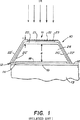
赤外線(IR)検出器の分野では、シリコン基板を含む第1の面の上方に配置された第2の面にマイクロブリッジを有する2レベルボロメータ放射検出器が用いられるのは公知である。例えば、米国特許第5,286,976号(以下「976号特許」と呼ぶ)および第5,300,915号(以下「915号特許」と呼ぶ)は、図1に示すような2レベル赤外線ボロメータ検出装置10を開示している。ボロメータとは、入射する電磁エネルギーを吸収し、吸収した入射電磁エネルギーを熱に変換することによって動作する電磁放射検出器である。976号特許および915号特許に開示されているボロメータ検出器は、高架マイクロブリッジ検出器レベル11と、下方レベル12とを有している。下方レベル12は、上面14に集積回路(IC)15の部品が形成された半導体基板13を含んでおり、ICの製造には従来のシリコンIC製造技術が使用されている。ICの部品は、ICを汚染から保護する窒化ケイ素の保護層16で被覆されている。高架マイクロブリッジ検出器レベル11は、窒化ケイ素層20、抵抗層21、窒化ケイ素層20および抵抗層21の上に配置された窒化ケイ素層22、ならびに、窒化ケイ素層22の上に配置されたIR吸収層23を含んでいる。製造工程において設けられた、下方に向かって延びている窒化ケイ素層20′および22′は、高架マイクロブリッジ検出器レベル11についての傾斜した支持脚となる。
915号特許および976号特許はまた、反射性材料の薄膜層18を下方レベル12に設けることができ、これにより高架マイクロブリッジ検出器レベル11と下方レベル12との間に空洞26を設けることができることを開示している。反射層18と上方マイクロブリッジ検出レベル11との間の垂直距離dは、層20、21、22および23を通過する入射エネルギーが層18によって上向きに反射させられるとともに、上方マイクロブリッジ検出レベル11に最初に入射するIRエネルギーと構造的に干渉特性を有するように選択される。特に、915号特許および976号特許は、反射されるエネルギーの位相が上方マイクロブリッジ検出レベルへの入射IRエネルギーの位相と一致するように、距離dを実質的に検出装置の動作の波長バンドの波長の4分の1になるように選択することを開示している。さらに、915号特許および976号特許は、高架マイクロブリッジ検出レベル11が入射IRエネルギーの検出器を含んでおり、検出器の活性領域(図示せず)をIR吸収層23および抵抗層21が構成するということを開示している。
当該技術分野で公知であるように、図1のボロメータ検出装置10の感度は、所望の動作波長バンドにおける装置の活性領域を構成する各材料の吸光係数、空洞構造26を含む検出器の物理的構造、マイクロブリッジ構造によって与えられる活性領域の熱隔離などをはじめとする多くの要因の関数である。図1では、空洞26およびマイクロブリッジ構造は、検出器の活性領域を周囲にあるもの、たとえば集積回路15から分離しており、活性領域が半導体基板13の上面14に配置された場合に得られるよりも高い分離を得ている。また、図1のマイクロブリッジ構造は、検出器が高架マイクロブリッジ検出レベルに配置され、バスライン、集積回路の部品などが下方レベル12に配置されているので、単一レベルボロメータ検出装置が基板13の中に配置されている場合よりも大きな充填率を可能とする。本明細書において、充填率は、検出器の活性領域である画素領域の割合として定義されることが理解されよう。また、画素領域とは、ボロメータ検出装置10を含む区域、言い換えるならば、高架マイクロブリッジ検出器レベル11および下方レベル12のIC回路の一方または両方を含む基板13面内の区域であることが理解されよう。言い換えるならば、画素充填率とは、活性領域を画素領域で割ったものである。さらに、ボロメータ検出器10の画素収集領域とは、検出装置がエネルギーを吸収する範囲の区域、言い換えるならば、検出装置が入射エネルギーに応答する範囲の区域であることが理解されよう。
第915号特許は、ボロメータ検出装置の充填率を最大限にし、ひいてはボロメータ検出器10の感度を増大させるために、高架マイクロブリッジ検出レベル11の活性領域を最大限にすることを開示している。つまり、第915号特許は、活性領域を上層マイクロブリッジレベル11に配置することによってボロメータ検出装置の分離を強めることおよび活性領域のサイズを最大限にすることにより、検出装置10の感度を増大させることを開示している。加えて、第976号特許は、動作バンドでの入射IR放射の吸収を最大限にするため、所望の動作波長バンドでピーク吸収を達成するようにすべての層20、21、22、23の厚さtおよび上層レベル11と反射層18との間の距離dを選択することを開示している。より詳細には、層20〜23の厚さtは、マイクロブリッジレベル11の熱量を最適化して所望の動作波長バンドでピーク吸収を達成するように選択され、距離dは、活性領域で最初は吸収されず層18から反射されるエネルギーと、最初に上層マイクロブリッジレベル11に入射するIRエネルギーとの間で構造的干渉を達成するように選択される。
関連技術の検出装置10に伴う一つの問題は、画素収集領域が実質的に検出装置の活性領域と同じであることである。例えば、活性領域は、1辺の長さが約50ミクロンの最小正方形領域(約2ミル×2ミル)となるように製造されてよい。しかしながら、画素領域を減少させることにより、例えば、1〜2波長の範囲の長さ(8〜12μmの範囲の波長動作範囲に対して1辺0.5〜1ミルに相当する)の辺を有する画素領域とすることにより、高解像度検出装置を提供することが必要とされている。さらに、大型検出装置の感度および時定数を維持する必要があるとともに、小型検出装置の感度および時定数は劣化させられるべきではない。言い換えると、従来の検出装置の感度および時定数を維持しつつ、より狭い画素領域またはより小さい画素サイズを有する検出装置を提供することが必要とされている。解像度を上げる一つの方法は、検出器の活性領域を小さくすることである。検出装置の時定数(tc)は、検出器の熱容量を熱コンダクタンスで割ったものに等しいことが知られている。つまり、検出装置10の活性領域が縮小されるにつれて、熱容量が小さくなり、それにつれて時定数が小さくなる。従って、検出装置の時定数と、活性領域のサイズまたは検出器の解像度との間にはトレードオフ関係が存在する。特に、活性領域(例えば、抵抗層21のエリア)のサイズを小さくすると、時定数が小さくなるということになる。よって、検出装置の熱容量の減少をオフセットし且つ検出装置の時定数を維持するために、検出装置の熱コンダクタンスを増大させる必要がある。
さらに、検出装置10の活性領域のサイズを小さくすると、より少ない入射エネルギーがより小さい活性領域で吸収されるようになる。なぜなら、小さい活性領域に入射するエネルギーは、大きな活性領域があった装置の一部分にはもはや吸収されないからである。これにより、検出装置の感度が減少することになる。つまり、検出装置の感度と、活性領域のサイズまたは検出器の解像度との間にはトレードオフ関係が存在する。従って、活性領域のサイズを減少させつつ、従来の検出装置の感度および時定数を維持する必要がある。
検出器アレイから遠く離れた景色または画像を検出器アレイ上に合焦させて検出器アレイの画素収集領域を効率的に増加させるために、検出器アレイの上方にレンズシステムを配置することが試みられている。例えば、米国特許第4,754,139号(以下、「139号特許」と呼ぶ)は、複数の検出器と、検出器アレイと遠くの画像または景色との間に配置された放射集結器とを含むIR焦点面アレイを開示している。放射集結器のアレイは、遠くにある画像または景色を検出器アレイ上に合焦させるために用いられ、検出器平面上に実質的なデッドスペースを生じることなく検出器を広く離隔させることを意図的に可能としている。
しかしながら、139号特許に示されているようなレンズシステムの問題点は、139号特許に示されているような構造を製造するのが非常に困難なことである。例えば、レンズは構造を複雑にし且つ装置のコストを増やす。従って、製造プロセスを複雑にすることなく且つ実質的なコスト増加をきたすことなく、検出層の画素収集領域を増加させ、画素収集領域を検出装置の活性領域の範囲よりも大きくすることができる構造を製造できることが必要とされている。より詳細には、活性領域によって吸収されない入射エネルギーを活性領域に戻して集結することが必要とされている。
発明の概要
従って、本発明の目的は、従来のマイクロブリッジ検出器構造を改良することである。また、本発明の目的は、大きな活性領域の検出器の吸収感度および熱的時定数を維持しつつ、縮小された活性領域を有するマイクロブリッジ検出器構造を提供することである。さらに、本発明の目的は、入射エネルギーを縮小された活性領域に集結する一体型集結器を有するマイクロブリッジ検出器構造を提供することである。
本発明の一つの観点によると、マイクロブリッジ検出器には、マイクロブリッジ検出器の画素収集領域よりも小さい活性領域が設けられている。マイクロブリッジ検出器は、集積回路を備える半導体基板と、この半導体基板の上方に配置されたマイクロブリッジとを含んでいる。マイクロブリッジは、検出器の活性領域よりも大きい画素収集領域を有する活性領域を含んでいる。加えるに、マイクロブリッジ検出器は、マイクロブリッジと半導体基板との間に熱隔離ギャップが存在するように、マイクロブリッジとつながっており、且つ、半導体基板の上方にマイクロブリッジを支持する、熱及び電気伝導性の下方伸延脚部であって、活性領域と半導体基板の集積回路とを電気的に接続する下方伸延脚部を含んでいる。
本発明の一実施の形態では、吸収領域と透過性窓とが交互になるように活性領域がパターン加工されている。本発明の別の実施の形態では、活性領域が、マイクロブリッジの実質的な中心部に配置された実質的に矩形の領域であり、下方伸延脚部は、活性領域の周りに螺旋状に巻かれてアンテナのように機能することによって、入射電磁放射を吸収し且つ入射電磁放射を活性領域と接続する。本発明のさらに別の実施の形態では、マイクロブリッジと半導体基板との間に傾斜壁を有する集結器が配置されている。集結器は、最初に活性領域で吸収されなかった入射放射を活性領域に向けて戻すように反射する。
このような構成によって、マイクロブリッジ検出器には、大きな活性領域を有する検出装置の感度および熱的時定数を維持しつつ、マイクロブリッジ検出器の活性領域よりも大きい画素収集領域が設けられる。特に、このような構成により、マイクロブリッジ検出器は、例えば、入射放射の動作波長の0.5〜2波長の範囲の画素解像度で製造され得る。例えば、一辺の長さが入射放射の3波長よりも大きい活性領域を有するマイクロブリッジ検出器は、大きな活性領域の装置のものと同等の光吸収感度を維持している。それに加え、このような構成により、マイクロブリッジ検出装置には、既存の製造技術を用いてマイクロブリッジと半導体基板との間に配置された集結器が形成される。従って、製造プロセスを複雑にすることなく追加コストを要することもなくマイクロブリッジ検出器を製造できる。
本発明の別の観点によると、マイクロブリッジ検出器は、集積回路を備える半導体基板と、この半導体基板の上方に配置されたマイクロブリッジとを含んでいる。マイクロブリッジは活性領域を含んでいる。加えるに、マイクロブリッジ検出器は、マイクロブリッジと半導体基板との間に熱隔離ギャップが存在するように、マイクロブリッジとつながっており、且つ、半導体基板の上方にマイクロブリッジを支持する、熱及び電気伝導性の下方伸延脚部であって、活性領域と半導体基板の集積回路とを電気的に接続する下方伸延脚部を含んでいる。さらに、マイクロブリッジ検出器は、検出器の活性領域よりも大きいマイクロブリッジ検出器の収集領域において入射放射を収集するための手段を含んでいる。
本発明の一実施の形態では、収集するための手段は、吸収領域と透過性窓とが交互になるようにパターン加工された活性領域を含んでいる。本発明の別の実施の形態では、活性領域は実質的に矩形の領域であり、マイクロブリッジレベルの実質的な中心部に配置されている。また、収集するための手段は、下方伸延脚部を含んでおり、下方伸延脚部は、活性領域の周りに螺旋状に巻かれており、アンテナのように機能することによって、入射電磁放射を吸収し、入射電磁放射を活性領域と接続する。本発明のさらに別の実施の形態では、収集する手段が傾斜壁を有する集結器を含んでおり、集結器は、マイクロブリッジレベルと半導体基板との間に配置されて、最初に活性領域で吸収されなかった入射放射を活性領域に向けて戻すように反射する。
また、このような構成により、マイクロブリッジ検出器には画素領域が設けられており、この画素領域はマクロブリッジ検出器の活性領域よりも大きいが、大きな活性領域を有する装置の光感度および熱的時定数を維持している。特に、このような構成でマイクロブリッジ検出器が製造されることができ、たとえば、ある決められた画像解像度でマイクロブリッジ検出器を製造することができる。ある決められた画像解像度とは、たとえば、入射放射の動作波長の0.5〜2波長の範囲の画素解像度である。このとき、マイクロブリッジ検出器は、たとえば、一辺の長さが入射放射の3波長よりも大きい活性領域を有するマイクロブリッジ検出器のような大きな活性領域をもつ装置の光吸収感度と同様の光吸収感度を維持している。加えるに、このような構成により、マイクロブリッジ検出装置には、既存の製造技術を用いてマイクロブリッジと半導体基板との間に配置された傾斜壁を有する集結器が形成され、従って、製造プロセスを複雑にすることなく、且つ、追加コストを要することなく製造できる。
本発明の別の観点によると、マイクロブリッジ検出器は、集積回路を備える半導体基板と、この半導体基板の上方に配置されたマイクロブリッジとを含んでいる。マイクロブリッジは、吸収領域と透過性窓とが交互になるようにパターン加工されて、活性領域よりも大きいマイクロブリッジ検出器の画素収集領域をもたらす活性領域を含んでいる。加えるに、マイクロブリッジ検出器は、熱及び電気伝導性の下方伸延脚部を含んでおり、下方伸延脚部はマイクロブリッジの連続部であり、マイクロブリッジと半導体基板との間に熱隔離ギャップが存在するように半導体基板の上方にマイクロブリッジを支持している。さらに、下方伸延脚部は活性領域と半導体基板の集積回路とを電気的に接続する。
本発明の別の観点によると、マイクロブリッジ検出器は、集積回路を備える半導体基板と、この半導体基板の上方に配置されたマイクロブリッジとを含んでいる。マイクロブリッジは、マイクロブリッジの実質的な中心部に配置された実質的に矩形の活性領域を含んでいる。加えるに、マイクロブリッジ検出器は、熱及び電気伝導性の下方伸延脚部を含んでおり、下方伸延脚部はマイクロブリッジと半導体基板との間に熱隔離ギャップが存在するように活性領域の周りに螺旋状に巻かれており、半導体基板の上方にマイクロブリッジを支持している。さらに、マイクロブリッジ検出器は、活性領域と半導体基板の集積回路とを接続する下方伸延脚部内に含まれている導電性経路を含んでいる。導電性経路は、アンテナのように機能することによって、入射放射を吸収し且つ入射放射を活性領域と接続する。さらに、導電性経路は、入射放射に応答した活性領域の温度変化を示す信号を半導体基板の集積回路に接続する。
本発明の別の観点によると、マイクロブリッジ検出器は、集積回路を備える半導体基板と、この半導体基板の上方に配置されたマイクロブリッジとを含んでいる。マイクロブリッジは活性領域を含んでいる。加えるに、マイクロブリッジ検出器は傾斜壁を有する集結器を含んでおり、集結器は、マイクロブリッジと半導体基板との間に配置され、最初に活性領域で吸収されなかった入射放射を活性領域に向けて戻すように反射して、マイクロブリッジ検出器の活性領域よりも大きい画素収集領域を生成する。さらに、マイクロブリッジ検出器は熱及び電気伝導性の下方伸延脚部を含んでおり、下方伸延脚部は、マイクロブリッジの連続部であり、マイクロブリッジと半導体基板との間に熱隔離ギャップが存在するよう半導体基板の上方にマイクロブリッジを支持している。さらに、下方伸延脚部は活性領域と半導体基板の集積回路とを電気的に接続する。
本発明の別の観点では、マイクロブリッジ検出器を形成する方法が、半導体基板上に第1の絶縁層を積層する工程と、前記第1の絶縁層をエッチングし、前記第1の絶縁層内に傾斜側壁を形成する工程と、前記第1の絶縁層をマスクしてエッチングすることにより、前記第1の絶縁層を通って前記半導体基板上のコンタクトパッドまでのコンタクトホールを形成する工程と、前記第1の絶縁層の前記傾斜側壁上および前記コンタクトホール内の前記第1の絶縁層を貫いて薄膜金属層を積層し、反射性集結器と前記反射性集結器を前記コンタクトパッドに接続する金属結線とを形成する工程を含んでいる。この方法は、さらに、前記薄膜金属層上に犠牲層を積層し、前記反射性集結器を実質的に充たすとともに実質的に平坦な表面を形成する工程と、前記平坦な表面上に支持層を積層する工程と、前記支持層上に高TCRの抵抗材料を積層する工程と、前記抵抗材料をマスクしてエッチングすることにより、前記マイクロブリッジ検出器の活性領域を形成する工程とを含んでいる。この方法は、さらに、前記支持層をマスクして前記支持層および前記犠牲層をエッチングすることにより、前記支持層および前記犠牲層を通って前記反射性集結器に達するコンタクトホールを形成する工程と、前記コンタクトホール内の前記支持層および前記犠牲層を貫いて第2の薄膜金属層を積層する工程と、前記第2の金属層をマスクしてエッチングすることにより、前記反射性集結器と前記活性領域との間に導電性経路を形成する工程とを含んでいる。さらに、この方法は、前記抵抗層および前記支持層をマスクしてエッチングすることにより、前記マイクロブリッジ検出器の前記活性領域を形成するとともに、前記活性領域の外側の前記犠牲層を露出させる工程と、前記犠牲層を溶融し、前記半導体基板上に配置された前記活性領域を有するマイクロブリッジレベルを含むマイクロブリッジ検出器構造を形成する工程であって、前記マイクロブリッジが前記マイクロブリッジ検出器の前記活性領域よりも大きい画素収集領域を有するような工程とを含んでいる。
本発明の別の観点のイメージングシステムは、電磁信号を受信し、前記電磁信号を合焦させ、その合焦信号を焦点面アレイに出力する光学素子を含んでいる。焦点面アレイは複数の検出装置を含んでおり、各検出装置がマイクロブリッジ検出器の活性領域よりも大きい画素収集領域を有しており、各検出装置が合焦信号を感知信号に変換しさらに前記感知信号を出力することによって、複数の感知信号を焦点面アレイプロセッサに供給する。焦点面アレイプロセッサは、複数の感知信号を受信し、前記複数の感知信号を処理して前記複数の感知信号間のすべてのゲインおよびすべてのオフセットエラーを修正し、複数の処理済み信号を表示プロセッサに出力する。表示プロセッサは、前記複数の処理済み信号を受信し、前記複数の処理済み信号を表示装置に出力するのに適した表示信号に変換する。表示装置は、前記表示信号を受信し、前記電磁信号を発する風景または物体の画像を表示するために前記表示信号を表示する。
イメージングシステムの実施の形態によると、イメージングシステムは、ヘルメット搭載イメージングシステム、ゴーグル搭載イメージングシステム、単眼システム、双眼システム、武器照準器、カムコーダ、顕微鏡、放射計および分光計のいずれかであってよい。
【図面の簡単な説明】
以下の詳細な説明を以下の図面と併せて参照すると、本発明の他の目的および特徴が明確になる。図面は例を示すだけのものであり、本発明の範囲を定義しようとするものではないことが理解されよう。
以下の図面から、前記およびその他の目的および利点がより十分に認識されるであろう。
図1は、従来の高架マイクロブリッジ検出レベルを有する2レベル検出装置を示し、
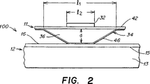
図2は、本発明による検出装置の一実施の形態の側面図であり、
図3は、図2の検出装置のマイクロブリッジレベルの平面図であり、
図4は、図2〜3の検出装置のさまざまな製造工程を示す図であり、
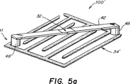
図5aは、本発明の別の実施の形態による検出装置の斜視図であり、
図5bは、図5aの検出装置の断面図であり、
図6aは、本発明の別の実施の形態によるマイクロブリッジレベルの平面図であり、
図6bは、図6aの検出装置の断面図であり、
図7は、本発明の別の実施の形態によるマイクロブリッジレベルの平面図であり、
図8aは、本発明の別の実施の形態によるマイクロブリッジレベルの平面図であり、
図8bは、図8aの検出装置の断面図であり、
図9は、本発明による図2〜8aに示された検出装置の実施の形態のいずれかを利用した検出装置アレイの斜視図であり、
図10は、本発明のイメージングシステムのブロック図を示し、
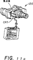
図11a、11bおよび11cは、図10のイメージングシステムの頭部装着実施の形態のヘルメット搭載設計およびゴーグル搭載設計をそれぞれ示し、
図12は、図11aおよび11bおよび11cの頭部装着イメージングシステムのブロック図を示し、
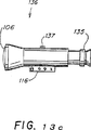
図13a、13bおよび13cは、図10のイメージングシステムの別の実施の形態である手持ち式イメージングシステムを示しており、特に、図13aが単眼システムを示し、図13b〜13cが双眼システムを示し、
図14aおよび14bは、図10のイメージングシステムの別の実施の形態である武器照準器を示しており、特に、図14aが武器照準器の平面図を示し、図14bが武器照準器のブロック図を示し、
図15aおよび15bは、図10のイメージングシステムの別の実施の形態であるカメラ/レコーダ(カムコーダ)を示しており、特に、図15aがカムコーダの断面図を示し、図15bがカムコーダのブロック図を示し、
図16aおよび16bは、図10のイメージングシステムの別の実施の形態である顕微鏡を示しており、特に、図16aが顕微鏡の側面図であり、図16bが顕微鏡の動作ブロック図であり、
図17aおよび17bは、図10のイメージングシステムの別の実施の形態である放射計/分光計システムを示しており、特に、図17aが結像放射計/分光計の断面図を示し、図17bが結像放射計/分光計のブロック図を示す。
詳細な説明
図2は、本発明による検出装置100の第1の実施の形態の側面図である。本明細書において、検出装置は、例えば検出された電磁信号の結果として、感知素子内での感知された温度変化に反応して電気信号を供給する感知素子を含むすべてのデバイスを意味しているものと理解されよう。検出装置は、例えば、ボロメータ検出器、光子検出器、強誘電体検出器、ダイオード検出器などであってよい。また、感知素子は、例えば温度、応力などの物理パラメータを測定するすべての構造を意味していると理解されよう。なお、図1の部材と同様の部材は同様の符号で示されている。
図1に関して上述したように、本発明の検出装置100は、高架マイクロブリッジ検出レベル11と下方レベル12とを有している。本発明において、マイクロブリッジは何らかの面の上方に浮架されたすべての構造を意味していると理解されよう。下方レベル12は、その上部に集積回路15要素が製造された半導体基板13を含んでいる。例えばダイオード、FET、バスライン、接続線、コンタクトパッドなどの多数の要素が通常の製造技術を用いて製造され且つこれらの要素の製造が意図されたものであることが理解されよう。特に、参考に組み込まれる1995年8月30日に出願された係属中の米国特許出願08/521,266号に開示されているような検出器または検出器アレイの電子的読み出し回路を、半導体基板13に配置することができ且つそれが意図されている。
図1に関して説明したように、図1に開示されたような活性領域の大きい関連技術の検出装置の吸収感度および熱的時定数を維持しつつ、検出装置の活性領域のサイズを減少させることが必要とされている。式(1)を参照すると、検出器の時定数(tc)は、検出装置の熱容量(C)を検出装置の熱コンダクタンス(G)で割ったものに等しいことが当業者には公知である。
(1) tc=C/G
検出装置の熱容量は、検出装置の活性領域のサイズに比例し、熱コンダクタンスは、マイクロブリッジレベル11の活性領域と下方レベル12の基板とを接続する伝導性脚部(図3の38、40参照)の長さ(l)に比例する。言い換えると、検出装置の活性領域が小さくなるにつれて、熱容量は減少しそして時定数tcも低下する。さらに、上述したように、活性領域のサイズが小さくなると、検出装置の吸収感度が低下する。つまり、検出装置の熱的時定数および感度のそれぞれと、検出装置の活性領域のサイズとの間にはトレードオフ関係がある。従って、本発明の検出装置は、活性領域が大きい検出装置の熱的時定数および感度を維持しつつ、検出装置の活性領域のサイズを減少させようとするものである。
本発明の検出装置は、活性領域が大きい検出装置の熱的時定数を維持するという上述の目的を、検出装置の熱コンダクタンス(G)を低下させること、言い換えると、活性領域が大きい検出装置の所望の時定数を維持するために検出装置の熱的隔離/抵抗を増加させることにより達成する。特に、マイクロブリッジレベルの活性領域と半導体基板とを接続する伝導性脚部の長さlは、所望の時定数を維持するために、活性領域のサイズの減少に反比例して増加させられる。例えば、本発明の好適な実施の形態によると、時定数は、8〜12μmの動作範囲波長バンドでは5〜20ミリ秒の範囲である。
さらに、上記した大きな活性領域の装置の感度を維持するという目的は、マイクロブリッジ検出器の活性領域よりも大きいマイクロブリッジ検出器の画素収集領域を生成する構造とすることにより達成される。ある実施の形態では、本発明の検出装置には、活性領域の大きな装置の光学的感度を維持しつつ、活性領域の小さい検出装置への入射エネルギー吸収を高める反射性集結器が備えられている。
より詳細には、図2に示された本発明の実施の形態によると、本発明は、マイクロブリッジレベル11と下方レベル12との間に反射性集結器34のあるマイクロブリッジ構造11を有する検出装置100を備えることにより、吸収感度を犠牲にすることなしに活性領域を削減するという問題を解決している。反射性集結器は、活性領域32により最初に検出されなかった活性領域からの入射IR放射を集結する。好ましくは、反射性集結器34は、約1〜2波長(8〜12μmの範囲の光学波長範囲について0.5〜1ミルに相当する)の範囲の辺l1を有する画素収集領域を有しており、活性領域は、約1/2波長(8〜12μmの範囲の光学波長範囲について約0.2ミルに相当する)の範囲の辺l2を有している。光学収集器34は、活性領域の領域よりも大きい検出装置の画素収集領域を生成するように機能する。
さらに、図2〜3に示された本発明の実施の形態によると、本発明は、サイズを縮小された活性領域32を有するが、熱的時定数を維持するために熱抵抗または隔離を増加させた検出装置100のことである。熱抵抗または隔離の増加、言い換えると、熱コンダクタンスの減少は、活性領域のサイズ減少から生じる熱容量の減少を埋め合わせるために伝導性脚部39、40の長さlを増加させることにより達成される。好ましくは、所望の動作範囲での熱的時定数を維持するために、伝導性脚部の長さは実質的に等しい長さlにされている。図2の検出器の好適な実施の形態では、熱的時定数は5〜20ミリ秒の範囲である。
再度図1を参照すると、本明細書においては、画素収集領域は、検出装置に入射したエネルギーを検出装置が収集する領域として定義されることが理解されるであろう。また、活性領域は、IR吸収層23および抵抗層21のいずれか一方または両方を含む総ての領域として定義されることが理解されるであろう。さらに、画素領域は、ボロメータ検出装置10を含む領域、言い換えると、上層マイクロブリッジレベル11および下方レベル12のIC回路15のいずれか一方または両方を含む基板13の平面内の領域であることが理解されよう。さらに、充填率は、検出器の活性領域を含む画素領域の割合であることが理解されるであろう。
図3は、図2の検出装置の高架マイクロ検出器レベルの平面図である。この図面は、活性領域32と金属結線38および40との接続を示すために、活性領域が透明であるかのように示されている。好適な実施の形態では、金属結線は、活性領域の各辺39、41において活性領域の上面に接続されている。しかしながら、活性領域のいかなる部分への接続も可能であってそれも意図されていることが理解されるであろう。
上述したように、活性領域は抵抗層を含んでおり、またIR吸収層を含むこともできる。活性領域は入射IR放射を吸収し、吸収されたIR放射を熱に変換する。この結果としての活性領域の温度変化は、温度変化の関数である活性領域の抵抗の変化を測定することにより感知される。
図2を参照すると、集結器34は、上方マイクロブリッジ11と集結器34の底部との間が距離dとなるような形状であり、集結器34全体の形状は、最初に活性領域32に吸収されず集結器34で反射されたエネルギーと活性領域32に最初に入射したエネルギーとが構造的に干渉特性をもたらすようにされる。マイクロブリッジレベル11の光学特性は、適切な光学的および電気的特性を持つ材料を適切に選択することにより達成されることが理解されよう。特に、層42は、入射IR放射をほとんど反射せずそのかなりの割合を集結器34側に投下するように選択され、集結器34は入射IR放射を活性領域32に集結し、画素収集領域の増大がもたらされる。金属結線38および40は、活性領域32の各辺39および41に接続されており、検出信号を下方レベル12の集積回路15に与える。検出信号は、感知された活性領域32の抵抗の変化に対応している。金属結線38および40は、集結器34の下方傾斜壁46が下方レベル12方向に向けてつながり、且つ、下方レベル上に配置されるパッド43および44と電気的に接続されるように構成され且つ配置されている。
上述したように、本発明の検出装置100は、脚部38および40の熱コンダクタンスを低下させることによって、活性領域のサイズの低下にもかかわらず熱的時定数を5〜20msの範囲に維持している。脚部の熱コンダクタンスは、以下の式で決定される。
(2) G=(K)(w)×(t)/l
ここで、Gは検出装置100の熱コンダクタンスであり、Kはマイクロブリッジレベルと基板との間に伝導性脚部38、40を設けるために用いられる材料の熱伝導率であり、wは脚部の幅であり、tは脚部を形成する材料の厚さであり、lは活性領域32と基板13上のコンタクトパッドとの間の脚部の長さである。これら寸法の検出装置を製造するために、脚部の幅wおよび厚さtは、通常製造技術および上方マイクロブリッジレベル11を支持することができるという要請によって制限される或るサイズに製造される。従って、検出器のコンダクタンスは、脚部の幅を狭くすることまたは脚部の厚みを減少させることによっては、好ましい時定数を達成するのに必要とされる値にまで低下させることができない。なぜなら、脚部の幅や厚みの寸法は製造技術により制限されるためである。
幅(w)および厚み(t)の寸法は製造技術で制限され且つ熱コンダクタンスはマイクロブリッジレベルと基板13との間の脚部38、40の長さ(l)に反比例するので、本発明によると、脚部の長さlが増大させられて熱的時定数が所望の動作範囲に維持される。しかしながら、脚部の長さ(l)を増大させるには、所望の熱コンダクタンスを達成し且つ熱的時定数を維持すべく脚部の長さ(l)を適切に増大させることができる十分なスペース36を、マイクロブリッジレベル11とレベル12との間に設ける必要がある。図2〜3に示された本発明の実施の形態によると、本発明では活性領域を削減することによって空いたスペースを利用している。特に、脚部38、40は活性領域の周りに巻き込まれ、適切な長さlとなって所望の時定数を達成している。
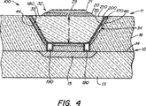
図2〜3の検出装置100は、マイクロブリッジレベル11と基板レベル12との間に反射性集結器34が設けられるという付加的な利点を伴って、既存のマイクロブリッジ製造技術を用いて製造される。より具体的には、図4を参照すると、標準的なICプロセスを用いて、基板13の表面14に集積回路15が製造されている。IC15および下方レベル12上には、例えばシリコン窒化物のような絶縁物16の層が積層されている。そして、集結器34の形状が、絶縁層16または絶縁層16の上面上に積層された付加された絶縁層(図示せず)内に形成される。集結器34の傾斜側壁46は、絶縁物の標準的な傾斜ドライエッチング技術を用いて形成され得る。後で詳述するように、集結器の形状および深さdは、製造される空洞構造および検出装置構造の詳細に依存している。
そして、反射性集結器34の表面35は、集結器上に積層される犠牲層180を取り去るための後のエッチングステップによってエッチングされない、例えばシリコン窒化物のような第2の絶縁層170によって保護される。例えば犠牲層は、例えばリン酸塩ガラスまたは非ドープガラスのような簡単に溶けるいずれかの材料であってよい。そして、第2の絶縁層をマスクし且つ基板レベル12(図3参照)の各コンタクトパッド43、44にまで、言い換えると集積回路15にまで第1および第2の絶縁層にコンタクト開口をエッチングすることによって、少なくとも1つのコンタクト開口190が第2の絶縁層170に設けられる。しかる後、例えば白金または金の金属フィルムのような反射性材料200の薄膜層が第2の絶縁層上に積層され、集結器34の反射性表面が形成されるとともに電気的集結器34からIC15のコンタクトパッド43、44への電気的接続がなされる。互いに電気的に分離された複数の検出装置100が設けられるように、反射性材料の薄膜層は画素領域の外側では取り去られることが理解されるであろう。
しかる後、非ドープガラス、リン酸塩ガラス、シリコンダイオードまたは他の容易に溶ける材料からなる犠牲層180が集結器の反射性表面200上に積層され、集結器を充たすとともに実質的に平坦な表面210が形成される。溶解性材料で充たされた集結器は、もし所望であれば、反射性集結器の薄膜金属上に積層された保護膜の第3の層(図示せず)を含むことができることが理解されるであろう。上述したように、反射性集結器34の最下点とマイクロブリッジレベル11との間の深さdは、集結器34で反射された入射電磁放射がマイクロブリッジレベル11、より詳細には活性領域32(図2〜3参照)に向かって反射され且つ活性領域32に入射した電磁放射と構造的干渉特性を有するように設けられる。本発明の集結器34の利益は、検出装置100の感度が増すと、検出装置の活性領域32の領域よりも大きな画素収集領域が与えられることである。さらに、集結器34の別の利益は、集結器34がないときに起こるよりも広い波長範囲にわたって吸収が達成されることである。
そして、実質的に平坦なマイクロブリッジ表面11上に、活性領域32のさまざまな層が積層される。特に、例えばシリコン窒化物のような第1の支持層20が、マイクロブリッジレベル11の実質的に平坦な表面上に積層される。しかる後、例えばバナジウム酸化物のような、大きな抵抗熱係数(TCR)を有する抵抗膜層21が、第1の支持層上に積層されて活性領域32が形成される。そして、抵抗膜層はマスクされ、活性領域32のパターンにエッチングされ活性領域32の外側の抵抗膜がエッチングで取り去られる。もし検出装置100の吸収効率を増加させることが必要であれば、例えばシリコン窒化物または薄い金属のような薄膜吸収層23が選択的に抵抗膜層上に積層されてよい。
大きなTCRの抵抗膜層21と集結器34の反射性金属層200との間の結線38、40は、所定パターンのマスクをして、マイクロブリッジレベル11の第1の支持層20および犠牲層180を通って下方の集結器34の反射性材料200までのコンタクトをエッチングすることにより形成される。しかる後、結線金属層(図示せず)が積層され、所定パターンのマスクがされ、抵抗膜層と反射性層との間に電気的コンタクト38、40が形成されるようにエッチングされる。なお、必要ではないものの、結線金属層を保護するために、保護膜材料の層が結線金属層上に積層されてもよい。
次に、吸収層23、抵抗膜層21および第1の支持層20がマスクされ、活性領域32の形状が定義される。そして、活性領域の外側領域は反射性集結器34を充たす犠牲層180までエッチングされ、実質的に犠牲層が露出する。その後、活性領域32が集結器34上に浮架され且つ下方基板レベル12から熱的に分離されつつ金属結線38、40によって基板レベル12と電気的に接続されるように、活性領域の層および反射層へ金属の結線を除去しないで犠牲層を除去する特定のエッチング工程を用いて犠牲層が溶融される。
本発明の図2〜3の実施の形態の利点は、通常の製造技術を用いて、活性領域32と基板レベル12との間に集結器34を形成できることであることが理解されよう。さらに、図2〜3の実施の形態の別の利点は、活性領域32の抵抗膜層21と基板レベル12の集積回路15とを接続する金属結線38、40を金属結線を設けるための反射性集結器の外側のスペースを用いる必要なく形成できることであることが理解されよう。
また、本発明によると、集結器34の幾何学的デザインは集結器34の全体的効果と比較すると重要ではないことが理解されよう。例えば、完全な放物反射器ではない集結器34でも、興味ある所望の動作波長バンドでは実質的に放物反射器のように機能する。図2〜3の実施の形態に示されているように、集結器34は例えば先端を切ったホルンアンテナ形状に曲げられてよい。しかしながら、最初に活性領域32に吸収されないエネルギーを活性領域32に集結するように機能して活性領域の範囲よりも大きな光学的収集領域を生成する当業者の知っているすべての形状は、本発明の範囲内であってかかる変形は意図されていることが理解されよう。その一つの例は放物反射器である。別の例が、本発明による検出装置の別の実施の形態の斜視図および断面図である図5a〜5bに図示されている。
図5a〜5bにおいて、同様の部材は同様の符号で示されている。図5a〜5bの実施の形態では、光学的集結器34′は図2〜3の曲面構造と異なり平坦構造である。図5a〜5bの実施の形態は、支持層42および活性領域32を支持する隔離絶縁器具48を含んでいる。図示されてはいないものの、図5a〜5bの実施の形態は、図2〜3に関して上述したように、半導体基板13および関連する集積回路15を含んでいてもよいことが理解されるであろう。他の点では、図5a〜5bの実施の形態は、図2〜3に関して上述したのと同様に動作する。特に、光学的集結器34′は入射エネルギーを活性領域32上に集結し、活性領域32の領域よりも大きい光学的収集領域を生成する。光学的集結器34′は、反射したエネルギーが集結器34′のすべての部分から活性領域32に同時に到着し且つ集結器34′が最初に活性領域32に入射したエネルギーを発展的に加えるように、集結器34′に入射したエネルギーを集結器の本体内で遅延させつつ光学的集結器34′の端部でエネルギーを即時に反射する。
図5a〜5bの検出装置構造100′を製造するには、反射性層18(図1参照)が図5a〜5bに示されているのと同様のパターンとなるようにパターン形成されるという付加的な利点を伴って、976号特許および915号特許に開示されているような既存の製造技術が用いられる。
本発明の図2〜5a〜5bの実施の形態の利点は、検出装置が、増加した画素収集領域を維持しつつ、例えば一辺の長さが動作波長範囲の半波長範囲であるサイズが削減され解像度が増加した活性領域を有していることである。加えるに、上記実施の形態の別の利点は、大きな活性領域をもつ装置と同等の光吸収感度および熱的時定数を有していることである(例えば、8〜14μmの範囲のエネルギーについて一辺の長さが3波長よりも大きい活性領域を有する)。本発明の好適な実施の形態においては、図2〜5a、5bの検出装置には、活性領域の一辺の長さが半波長範囲であることを維持しつつ、一辺の長さが1〜2波長の範囲である活性領域を有する装置と同等な光学的収集領域が設けられている。加えるに、図2〜4の実施の形態では、活性領域に空けられたスペースは、熱的時定数を5から20msの所望の動作範囲に維持するために、金属結線38および40の長さを増加させるために用いられる。従って、図2〜5a、5bの実施の形態は、活性領域の大きな装置の光吸収感度および熱的時定数を維持しつつ、画素解像度サイズをより小さくすることを達成している。
本発明の別の観点では、検出装置には、関連技術の装置の感度および時定数を維持しつつ、図1に示されたような関連技術の検出装置と比べて充填率が小さい活性領域が設けられている。特に、本発明のこの観点によると、検出装置の全体の充填率は減少するものの画素収集領域による入射エネルギーの吸収が維持されるように、吸収層23および高TCRの抵抗層21のいずれか一方または両方がパターン加工される。
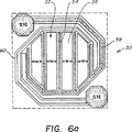
図6aおよび6bは、本発明による、小さくなった充填率を有する検出装置のマイクロブリッジレベルの平面図および断面図をそれぞれ示している。図6aの実施の形態50において、活性領域52は、交互に配置された導電領域54(吸収素子)および透過性窓56を含むようにパターン加工されている。特に、図6aおよび6bの実施の形態では、複数の直線状光吸収素子54が複数の透過性窓56の間に配置されている。直線状吸収素子54は、抵抗温度係数(TCR)の大きな材料の抵抗層を備えている。さらに、直線状吸収素子は、吸収材料の層を含んでもよいことが理解されるであろう。また、吸収材料は、高TCR材料の上に形成されるか、高TCR材料層の間に配置されるか、または、高TCR材料の下に配置されてよく、これらの変形は意図されたものであることが理解されるであろう。透過性窓56の幅wは、検出装置50に入射する放射の波長の所望動作範囲波長よりも実質的に小さくなるように選択される。幅wを適切に選択すると、吸収素子54による吸収は、図1に開示されたような固体活性領域と実質的に等しくなる。従って、本発明の利点は、例えば図1の関連技術のようなより大きな充填率の活性領域をもつ検出器の感度を維持しつつ、充填率がより低い活性領域が設けられることである。さらに、本発明の別の利点は、活性領域が、検出装置の活性領域よりも大きな画素収集領域をもつことである。
図6bを参照すると、反射性層18と上方レベル11との間の垂直距離dが描かれている。上方レベル11は、複数の吸収素子54と複数の透過性窓56を備えている。垂直距離dは、層18から反射した入射エネルギーが上方の吸収素子54に向けて反射され、且つ、例えば8〜14μmの好適な波長範囲においてほとんどの吸収がなされる干渉特性を有するように、好ましくは波長の1/4である。より詳細には、距離dは、トータルの経路長が半波長となって反射エネルギーと入射エネルギーとの構造的な和を達成するために、好ましくは波長の1/4である。図6aおよび6bには具体的に図示されていないけれども、図6a〜6bの活性領域は、図1〜5のいずれかに図示された検出装置の基礎として用いることができ、それが意図されていることが理解されるであろう。
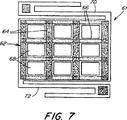
図6a〜6bに開示された実施の形態の一つの欠点は、吸収素子54の長手方向に直線偏光されることである。これに対して、図7は、本発明の別の実施の形態による検出装置61のマイクロブリッジレベルの平面図を示している。本実施の形態では、活性領域62は、複数の透過性窓68の間に配置された垂直吸収素子64および水平吸収素子66を含んでおり、グリッド構造を形成している。本発明のこの実施の形態の利点は、それが偏光されないということである。上述したように、伝導性リード線70および72は、マイクロブリッジレベルに配置された活性領域を支持し、また、活性領域からの感知信号を基板レベルに接続する。図7のマイクロブリッジレベル61の一実施の形態では、垂直吸収素子64および水平吸収素子66は、高TCR材料の抵抗層を備えている。しかしながら、垂直吸収素子64および水平吸収素子66のいずれか一方または両方は吸収材料の層を含んでもよいことが理解されよう。さらに、垂直吸収素子および水平吸収素子のいずれか一方または両方は、吸収層、高TCR材料の層、または吸収層と高TCR材料層の両方を含んでもよく、こういった偏光が意図されていることが理解されよう。図7のアクティブ素子の動作および利益は、これ以外は図6のアクティブ素子のものと同様である。特に、アクティブ素子は、固体活性領域の感度を維持しつつ削減された充填率を有しており、検出装置の活性領域よりも大きい画素収集領域を供給する。加えるに、図7の実施の形態の別の利益は、入射エネルギー収集に関して偏光されないことである。
図8aを参照すると、本発明のさらに別の実施の形態による検出装置のマイクロブリッジレベル74の平面図が示されている。特に、マイクロブリッジレベル74は、実質的にマイクロブリッジレベル74の中央に配置された活性領域76と、伝導性リード線78および80とを含んでいる。活性領域76は、図1の関連技術の活性領域に比べてサイズの縮小された、例えば一辺の長さが半波長の範囲の四角形の領域であって、高TCRの抵抗材料の層を含んでいる。また、活性領域は、上述したように、吸収層を含んでいてもよいことが理解されよう。さらに、伝導性リード線78および80は、導電層と高TCR材料の抵抗層とを備えている。また、リード線78、80は、吸収材料の層を含んでいてもよい。本発明のこの実施の形態によると、活性領域76および脚部78、80が一緒になって装置の効果的な活性領域を生成する。特に、脚部78および80は螺旋形状にパターン加工されてアンテナとして機能し、螺旋状伝導性リード線78および80に入射するエネルギーがマイクロブリッジレベル74の中心部の活性領域に結びつけられる。また、脚部78および80は、活性領域76の感知された温度変化を反映した検出信号を下方レベル12と結びつけるように働く。つまり、伝導性脚部78および80は、図8aおよび8bの実施の形態では2つの目的を有している。
上述したように、この実施の形態の利益は、図1に示されたような関連技術の装置の全活性領域と比較したとき、関連技術の装置の感度を維持しつつ、四角形の領域76および脚部78、80を含む全活性領域が、縮小された充填率を有しているということである。さらに、別の利益は、装置が活性領域よりも大きい画素収集領域を有しているということである。
図8bは、図8aのマイクロブリッジ検出装置の側面図を示している。マイクロブリッジレベル74と反射器18との間の垂直距離dは、反射性層18に入射するすべての放射をマイクロブリッジレベル74に向けて反射するため、および、例えば8〜14μmの好適な波長範囲においてほとんどの吸収がなされる干渉特性を有するように、好ましくは1/4波長である。特に、距離dは、実質的に装置の動作範囲波長の1/4波長であることが好ましい。
図6a、6b〜8a、8bの検出装置を製造するには、高TCR材料の抵抗層および吸収層の少なくとも1つがマスクおよびエッチングされて図6a、6b〜8a、8bのそれぞれに開示されているような活性領域をパターン形成するという点を除いて、976号特許および915号特許に開示されているような既存の製造技術が用いられる。
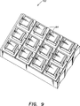
上述の説明は個々の検出装置に関してなされたものであるが、本発明はアレイアセンブリ、特に複数の検出装置がxおよびy方向にあって焦点面アレイを形成するアレイにも適用される。特に、図9は、マイクロブリッジ検出装置84の焦平面アレイ102の斜視図を示している。また、上述した図2〜8bに示されたすべてのマイクロブリッジ検出装置が図9のアレイに用いられることが理解されよう。本発明の一実施の形態では、x方向に沿った列に327個の検出装置が配置されておりy方向に沿った行に245個の検出器が配置されているアレイが、半導体基板上に設けられており、各検出器または画素装置は一辺で約46ミクロンの領域に及んでいる。半導体アレイは8〜14μmのIR波長範囲にわたって動作し、少なくとも80%のIR感度を有している。
本発明の非冷却焦点面アレイ102は、図10のブロック図に示すようなイメージングシステム104に使用することができることが理解されよう。図10のイメージングシステムでは、光学部品106に入射する二つの動作波長バンドの電磁放射、たとえば波長範囲8〜14μmおよび3〜5μmの赤外線放射が光学部品、たとえばレンズによって焦点を合わされ、合焦された電磁信号を出力107に提供する。合焦された電磁信号は非冷却焦平焦点面面アレイ102に結像される。焦点面アレイが、合焦された電磁信号を複数の感知信号に変換し、これらの信号が媒体109を介して焦点面アレイプロセッサ108に出力される。焦点面アレイプロセッサ108は、たとえば、複数の感知信号をデジタル化して複数の処理済み信号を提供し、その複数の処理済み信号を、焦点面アレイの複数の検出装置の間のゲイン差または他の不均一さに関して調節することにより、複数の感知信号を処理する。そして、複数の処理済み信号が媒体111を介して表示プロセッサ110に出力される。表示プロセッサは、複数の処理済み信号を再度フォーマットして、表示装置112に表示するのに適したフォーマットの複数の表示信号にし、媒体113を介して表示信号を表示装置に出力する。表示プロセッサは、当業者に公知である処理済み信号のすべての表示処理、たとえば、表示信号への再フォーマット処理、不良画素データを除去する処理、焦点調節処理、記号および/または他の情報を表示信号に付加する処理、明るさおよび/またはコントラストを調節する処理などをも実行することができることが理解されよう。制御装置114が、表示プロセッサの自動および/または手動の制御を提供して、たとえば明るさ、コントラスト、記号の付加などの種々の表示パラメータの自動および/または手動の調節を可能にする。イメージングシステムは、電池、AC電源またはDC電源のいずれか一つを含むことができる電源電子部品116によって給電される。
図10のイメージングシステムは、通常、システムの操作者が見る像の二次元リアルタイム表示を提供する。たとえば、本発明のイメージングシステムの好ましい実施の態様では、非冷却焦点面アレイ102は、対象の外線(IR)波長バンドの少なくとも一つで動作するように設計されている。このシステムによると、操作者は、通常は人の目で見ることができないような条件の下で物体および/または景色の熱サインを見ることができる。たとえば、イメージングシステムは、夜間に、放射物質降下条件の無い昼間に、煙の存在で、または悪化した天候条件で使用することができる。
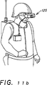
本発明の焦点面アレイを使用することができる熱型イメージングシステムの一例は、図11a〜11cに示す頭部装着イメージングシステム120である。図11aは頭部装着イメージングシステムのヘルメット搭載設計を示し、図11bは頭部装着イメージングシステムのゴーグル設計を示し、図11cはイメージングシステム自体の拡大図を示す。
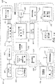
図12は、図11a〜11cの頭部装着イメージングシステムのブロック図を示す。図10に示すイメージングシステムと同様の部品は、同様な参照符号によって示され、それらの部品の説明はここでは繰り返さないことが理解されよう。図12の頭部装着イメージングシステムでは、電磁信号が光学部品106によって焦点面アレイ102に合焦される。焦点面アレイ102は、焦点面アレイプロセッサ108に含まれる温度安定化回路124によって温度安定化される。焦点面アレイ102は、合焦信号を感知信号に変換し、複数の感知信号を焦点面アレイプロセッサ108に出力する。焦点面アレイプロセッサは、前置増幅アナログ・デジタル変換器126によって複数の感知信号それぞれを増幅およびデジタル化し、複数の処理済み信号を表示プロセッサ110に出力する。焦点面アレイプロセッサはまた、複数の処理済み信号を処理して、複数の処理済み信号の間に何らかのオフセットまたはゲインの差があるならばそれを修正して、不良信号データを除去するプログラム可能な論理素子128を含んでいる。表示プロセッサは、修正済み信号を再フォーマットし、修正済み信号をデジタル・アナログ変換器130によってアナログ信号に変換して、アナログ信号が表示装置に適したフォーマットになるようにする。そして、表示装置ドライバ132がアナログ信号をユーザに表示するために表示装置112に出力する。
上で論じたように、制御装置114は、表示プロセッサの自動および/または手動の制御を提供して、種々の表示パラメータの自動および/または手動の調節を提供する。頭部装着システムの制御装置は、制御パネル中のスイッチ類115と、マイクロプロセッサ117とを含む。加えて、電源電子部品116は、電池119または外部電源121へのコネクタと、電源状態回路123とを含む。さらに、表示プロセッサ110は、複数の処理済み信号を表示信号にフォーマットし直し、表示装置上に記号を提供するための記号生成器125を含む。
頭部装着システム120の好ましい実施の態様では、焦点面アレイ102は、少なくとも一つのIR波長バンド、たとえば8〜14μmの範囲で動作する。加えて、表示装置112は、システムユーザにとって単眼表示装置または両眼表示装置のいずれであってもよく、制御装置114を用いて調節することができる。好ましい実施の態様では、焦点面アレイプロセッサ108および表示装置112は、ヘルメットの中または顔面装着ゴーグルの中に搭載される。加えて、表示プロセッサ110、制御装置114および電源116は、ベストに装着することができるユニットに搭載される。しかし、当業者に公知である変形、たとえば上記それぞれをヘルメットまたはゴーグルに搭載する形態が考慮され、本発明の範囲に入るものとみなされる。
頭部装着イメージングシステムの利点は、それが、サイズ、重量および電力消費を減少させた独立型の携帯式ユニットであることにある。具体的には、焦点面アレイは、従来技術の装置に求められるような冷却または機械的スキャナもしくはチョッパを要しない。加えて、頭部装着システムは、暗闇でも動作することができ、昼間には、イメージ増倍管を使用する従来技術の装置とは対照的に、放射物質降下なしで動作することができ、煙を透視するなどができる。さらに、ボロメータ検出装置および焦点面アレイに関して上記に論じた理由から、頭部装着システムは、従来技術の装置に比べて改善された信頼性および感度を有する。
本発明の焦点面アレイを使用するイメージングシステムのもう一つの例は、図13a、13bおよび13cに示すような手持ち式イメージングシステムである。手持ち式イメージングシステムは、図13aに示すような単眼システム134であることもできるし、図13bおよび13cに示すような双眼システム136であることもできる。図10のイメージングシステムに類似する部品は、同じ参照符号がつけられており、それらの要素の説明は繰り返さないことが理解されよう。図13aの単眼システムは、IR光学部品106の前方に配置された光学フィルタ122を有するウィンドウ127と、入射する電磁放射をIR光学部品に合焦させる合焦リング129とを有している。加えて、表示装置112は、CRTまたはFPD133と組み合わさって作用して表示を提供するアイピース131を含む。アイピース表示装置112はまた、当業者には公知であるように、視度調節135および合焦ノブ137を有している。図13a、13bおよび13cの手持ち式イメージングシステムの好ましい実施の態様では、電源電子部品116は電池であり、焦点面アレイは、少なくとも一つのIR波長範囲で動作して、暗闇でも昼間の光の下でも使用することができ、煙をも透視することができる長距離IR望遠鏡または双眼鏡を提供する。加えて、長距離望遠鏡および双眼鏡は、増大した信頼性および感度を提供しながらも、サイズ、重量および電力消費を減少させた独立型ユニットである。
本発明の焦点面アレイ102を使用することができるイメージングシステムのさらなる例は、図14a〜14bに示すような武器照準器140である。図14aは、本発明の武器照準器の平面図を示し、図14bは、図14aの武器照準器のブロック図を示す。図10のイメージングシステムと同様の部品は、同様の参照符号によって示されており、それらの要素の説明は繰り返さないことが理解されよう。武器照準器はまた、レンズ106を覆うカバー139と、レンズ106からの合焦信号の焦点を焦点面アレイ102上に調節するための合焦リング129と、コンパス141と、グローバルポジショニングシステム(GPS)アンテナ143とを含む。表示プロセッサ110は、GPS信号およびコンパス情報を処理するためのさらなる電子部品を含む。図14a〜14bの武器照準器の好ましい実施の態様では、光学レンズ106はフィルタをさらに含み、電源電子部品116は電池であり、表示装置112はアイピース、CRTもしくはFPD133および焦点調節ノブ135を含む。焦点面アレイの好ましい実施の態様は、少なくとも一つの所望の対象IR波長バンドで動作して、暗闇を透視し、煙を透視するように使用することができ、昼間でも使用することができるなどの長距離武器照準器、たとえばライフル銃のマウントを提供する。加えて、本発明の武器照準器140は、増加した信頼性および感度を提供しながらも、サイズ、重量および電力消費を減少させた独立型ユニットである。
本発明の焦点面アレイを使用することができるさらに別のイメージングシステムは、図15a〜15bに示すようなミニチュアカメラ/レコーダ(以下「カムコーダ」と呼ぶ)である。図15aはカムコーダの断面図を示し、図15bはカムコーダのブロック図である。図10のイメージングシステムに類似する部品は、同じ参照符号によって示されており、それらの要素の説明は繰り返さないことが理解されよう。カムコーダは、信号を適当な記録媒体154上に記録するためのレコーダ152を含む。記録媒体は、当業者に公知であるいかなる記録媒体、たとえばVHS、8mmまたはBETAフォーマットの磁気記録テープであってもよいことが理解されよう。カムコーダの好ましい実施の態様では、表示装置112は、ビューファインダ145およびCRTもしくはFPD133を含む。加えて、好ましい実施の態様では、電源電子部品116は充電式電池パックであり、制御装置114は、記録媒体を巻き戻し、早送りし、再生するための制御ノブ147および電子部品を含む。さらに、好ましい実施の態様では、焦点面アレイ102は、少なくとも一つの対象のIR波長バンドで使用して、夜間でも昼間でも使用することができ、煙または荒れた天候を透視するなどの長距離カムコーダを提供する。加えて、図15のカムコーダは、サイズ、重量および電力消費を減少させ、また、信頼性および感度が増大した独立型ユニットである。
本発明の焦点面アレイを使用することができるイメージングシステムのさらに別の実施の形態は、図16a〜16bに示すような顕微鏡160である。図16aは顕微鏡の側面図であり、図16bは顕微鏡のブロック図である。図10のイメージングシステムに類似する部品は、同じ参照符号によって示されており、それらの要素の説明は繰り返さないことが理解されよう。顕微鏡は、当業者には公知であるように、位置調節装置155を有する顕微鏡ベース153と、光源149によってバックライト照射される標本または集積回路マスク151とを含む。図16a〜16bの顕微鏡の好ましい実施の態様では、表示装置112はCRTまたはFPD133を含み、制御装置114は手動制御ノブ147を含み、光学部品106は正面の鏡157を含む。加えて、好ましい実施の態様では、焦点面アレイは、複数の対象IR波長バンド、たとえば3〜5μm、8〜12μmで使用することもできるし、フィルタ159を用いて可視光線範囲で使用して、マルチスペクトル像を顕微鏡に提供することもできる。
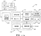
さらに、本発明の焦点面アレイを使用することができるもう一つのイメージングシステムは、図17a〜17bに示すようなイメージング放射計/分光計である。図17aはイメージング放射計/分光計170の断面図を示し、図17bはイメージング放射計/分光計のブロック図を示す。図10のイメージングシステムに類似する部品は、同じ参照符号によって示されており、それらの要素の説明は繰り返さないことが理解されよう。イメージング放射計/分光計では、レンズ106は、分光計を提供するために使用されるスペクトル分割レンズ172および放射計を提供するために使用される結像レンズ174のいずれか一方であってよい。イメージング放射計は、放射計が合焦された場面の温度を測定するのに使用され、分光計は、場面によって発されるエネルギーまたは出力を、その場面が電磁信号を発しているところの波長の関数として測定するのに使用される。
放射計/分光計はまた、スペクトル分割レンズ172および結像レンズ174のいずれかを取り付けるためのレンズマウント161と、放射計/分光計を三脚に取り付けるための三脚マウント163とを含む。放射計/分光計の好ましい実施の態様では、表示装置112はCRTまたはFPDを含み、制御装置114は手動制御ノブ147を含み、電源電子部品は充電式電池164および110ボルトACコネクタ165を含む。加えて、焦点面アレイは、少なくとも一つの対象のIR波長バンドで使用して、夜間に使用することもでき、昼間に放射物質降下なしで使用することもでき、煙を透視し、荒れた天候を透視することができる長距離放射計/分光計を提供する。さらに、放射計/分光計は、増大した信頼性および感度を有しながらも、サイズ、重量および電力消費を減少させた独立型ユニットである。
本発明の特定の実施の態様をいくつか説明したが、当業者にとって、種々の変形、修正および改良が容易に思いつくであろう。そのような変形、修正および改良は本開示の一部とみなされ、本発明の範囲および観点に入るものとみなされる。したがって、前記説明は例を示すものに過ぎず、本発明は、以下の請求の範囲およびその同等物のみによって定義される。This application claims the benefit of previously filed provisional application No. 60 / 007,909, entitled “Antenna-Coupled Thermal Microdetectors”, filed December 4, 1995.
Background of the Invention
1. Field of Invention
The present invention relates generally to uncooled infrared microdetectors, and in particular, the present invention relates to a thermal detector having a microbridge structure, in which the pixel infrared radiation collection region of the bolometer detector is on the microbridge structure. Relates to a thermal detector that is larger than the active region.
2. Explanation of related technology
In the field of infrared (IR) detectors, it is known to use a two-level bolometer radiation detector having a microbridge on a second surface disposed above the first surface including the silicon substrate. For example, US Pat. Nos. 5,286,976 (hereinafter referred to as “976 patent”) and 5,300,915 (hereinafter referred to as “915 patent”) disclose two-level infrared rays as shown in FIG. A
The 915 and 976 patents can also provide a
As is known in the art, the sensitivity of the
The '915 patent discloses maximizing the active area of the elevated
One problem with the related
Furthermore, when the size of the active region of the
Attempting to place a lens system above the detector array to focus a scene or image far away from the detector array onto the detector array to effectively increase the pixel collection area of the detector array It has been. For example, US Pat. No. 4,754,139 (hereinafter referred to as the “139 patent”) includes a plurality of detectors and a radiation concentrator disposed between the detector array and a distant image or scene. An IR focal plane array is disclosed. An array of radiation concentrators is used to focus distant images or scenes onto the detector array and is intended to widely separate the detectors without creating substantial dead space on the detector plane Is possible.
However, a problem with lens systems such as that shown in the '139 patent is that it is very difficult to produce a structure such as that shown in the' 139 patent. For example, the lens complicates the structure and increases the cost of the device. Therefore, a structure capable of increasing the pixel collection area of the detection layer and making the pixel collection area larger than the range of the active area of the detection device without complicating the manufacturing process and without substantially increasing the cost. There is a need to be able to manufacture. More specifically, it is necessary to collect incident energy that is not absorbed by the active region back to the active region.
Summary of the Invention
Accordingly, it is an object of the present invention to improve the conventional microbridge detector structure. It is also an object of the present invention to provide a microbridge detector structure having a reduced active region while maintaining the absorption sensitivity and thermal time constant of a large active region detector. It is a further object of the present invention to provide a microbridge detector structure having an integrated concentrator that concentrates incident energy into a reduced active area.
According to one aspect of the present invention, the microbridge detector is provided with an active area that is smaller than the pixel collection area of the microbridge detector. The microbridge detector With integrated circuit Semiconductor substrate and this semiconductor substrate of Up Direction And a microbridge disposed in the. The microbridge includes an active area having a pixel collection area that is larger than the active area of the detector. In addition, the microbridge detector is connected to the microbridge so that there is a thermal isolation gap between the microbridge and the semiconductor substrate, and the semiconductor substrate of Up Direction To support microbridge Of thermal and electrical conductivity Lower extension leg A downwardly extending leg for electrically connecting the active region and the integrated circuit of the semiconductor substrate. Is included.
In one embodiment of the present invention, the active region is patterned so that the absorbing region and the transmissive window alternate. In another embodiment of the present invention, the active region is a substantially rectangular region located at the substantial center of the microbridge, and the lower extension leg is spirally wound around the active region. By acting like an antenna, it absorbs incident electromagnetic radiation and connects it to the active region. In yet another embodiment of the invention, between the microbridge and the semiconductor substrate. With inclined walls A concentrator is arranged. The concentrator reflects incident radiation that was not initially absorbed in the active region back toward the active region.
With such a configuration, the microbridge detector is provided with a pixel collection area that is larger than the active area of the microbridge detector while maintaining the sensitivity and thermal time constant of a detector having a large active area. In particular, with such a configuration, the microbridge detector can be manufactured with a pixel resolution in the range of 0.5 to 2 wavelengths of the operating wavelength of incident radiation, for example. For example, a microbridge detector having an active region with a side length greater than three wavelengths of incident radiation maintains a light absorption sensitivity equivalent to that of a large active region device. In addition, with such a configuration, a concentrator disposed between the microbridge and the semiconductor substrate is formed in the microbridge detection device using an existing manufacturing technique. Therefore, the microbridge detector can be manufactured without complicating the manufacturing process and without additional costs.
According to another aspect of the invention, the microbridge detector comprises: With integrated circuit Semiconductor substrate and this semiconductor substrate of Up Direction And a microbridge disposed in the. The microbridge includes an active region. In addition, the microbridge detector is connected to the microbridge so that there is a thermal isolation gap between the microbridge and the semiconductor substrate, and the semiconductor substrate of Up Direction To support microbridge Of thermal and electrical conductivity Lower extension leg A downwardly extending leg for electrically connecting the active region and the integrated circuit of the semiconductor substrate. Is included. In addition, the microbridge detector includes means for collecting incident radiation in the collection area of the microbridge detector that is larger than the active area of the detector.
In one embodiment of the invention, the means for collecting includes an active region that is patterned such that the absorbent region and the transmissive window alternate. In another embodiment of the present invention, the active region is a substantially rectangular region and is located at the substantial center of the microbridge level. The means for collecting also includes a lower distraction leg that is helically wound around the active region and acts like an antenna, thereby providing incident electromagnetic radiation. Absorb and connect incident electromagnetic radiation with the active region. In yet another embodiment of the invention, the means for collecting is With inclined walls A concentrator is disposed between the microbridge level and the semiconductor substrate and reflects the incident radiation that was not initially absorbed in the active region back toward the active region.
Also, with such a configuration, the microbridge detector is provided with a pixel area, which is larger than the active area of the macrobridge detector, but the photosensitivity and thermal characteristics of a device with a large active area. The time constant is maintained. In particular, a microbridge detector can be manufactured with such a configuration, for example, a microbridge detector can be manufactured with a certain image resolution. The predetermined image resolution is, for example, a pixel resolution in the range of 0.5 to 2 wavelengths of the operating wavelength of incident radiation. At this time, the microbridge detector has an optical absorption similar to the optical absorption sensitivity of a device having a large active region, such as a microbridge detector having an active region whose side length is greater than three wavelengths of incident radiation. The sensitivity is maintained. In addition, with such a configuration, the microbridge detection device is arranged between the microbridge and the semiconductor substrate using the existing manufacturing technology. With inclined walls A concentrator is formed and can therefore be manufactured without complicating the manufacturing process and without additional costs.
According to another aspect of the invention, the microbridge detector comprises: With integrated circuit Semiconductor substrate and this semiconductor substrate of Up Direction And a microbridge disposed in the. The microbridge includes an active area that is patterned with alternating absorption and transmission windows to provide a pixel collection area of the microbridge detector that is larger than the active area. In addition, the microbridge detector Thermal and electrically conductive Includes lower distraction legs, lower Distraction The leg is a continuous part of the microbridge and the semiconductor substrate so that a thermal isolation gap exists between the microbridge and the semiconductor substrate. of Up Direction Supports a microbridge. further, The lower extension leg electrically connects the active region and the integrated circuit of the semiconductor substrate. .
According to another aspect of the invention, the microbridge detector comprises: With integrated circuit Semiconductor substrate and this semiconductor substrate of Up Direction And a microbridge disposed in the. The microbridge includes a substantially rectangular active region disposed at the substantial center of the microbridge. In addition, the microbridge detector Thermal and electrically conductive A lower extension leg that is spirally wound around the active region such that a thermal isolation gap exists between the microbridge and the semiconductor substrate; of Up Direction Supports a microbridge. Furthermore, the microbridge detector has an active region and a semiconductor substrate Integrated circuit And a conductive path included in a downwardly extending leg connecting the two. The conductive path functions like an antenna to absorb incident radiation and connect it to the active region. In addition, the conductive path sends a signal indicating the temperature change of the active region in response to incident radiation to the semiconductor substrate Integrated circuit Connect to.
According to another aspect of the invention, the microbridge detector comprises: With integrated circuit Semiconductor substrate and this semiconductor substrate of Up Direction And a microbridge disposed in the. The microbridge includes an active region. In addition, the microbridge detector With inclined walls A concentrator is disposed between the microbridge and the semiconductor substrate and reflects the incident radiation that was not initially absorbed in the active region back toward the active region, thereby detecting the microbridge. A pixel collection area that is larger than the active area of the vessel is generated. In addition, the microbridge detector Thermal and electrically conductive The lower extension leg is a continuous part of the microbridge, and the semiconductor substrate has a thermal isolation gap between the microbridge and the semiconductor substrate. of Up Direction Supports a microbridge. further, The lower extension leg electrically connects the active region and the integrated circuit of the semiconductor substrate. .
In another aspect of the present invention, a method of forming a microbridge detector includes: laminating a first insulating layer on a semiconductor substrate; etching the first insulating layer; and in the first insulating layer Forming a sloped sidewall in the step, forming a contact hole through the first insulating layer to a contact pad on the semiconductor substrate by etching the first insulating layer as a mask, and A thin-film metal layer is laminated on the inclined sidewall of the first insulating layer and through the first insulating layer in the contact hole, and the reflective concentrator and the reflective concentrator are connected to the contact pads. Forming a metal wire. The method further includes the step of laminating a sacrificial layer on the thin film metal layer to substantially fill the reflective concentrator and form a substantially flat surface; and a support layer on the flat surface. Laminating, laminating a high TCR resistive material on the support layer, and forming an active region of the microbridge detector by masking and etching the resistive material. . The method further includes forming a contact hole reaching the reflective concentrator through the support layer and the sacrificial layer by etching the support layer and the sacrificial layer while masking the support layer. Laminating a second thin film metal layer through the support layer and the sacrificial layer in the contact hole, and etching the second metal layer while masking the reflective concentrator and the Forming a conductive path between the active region and the active region. Furthermore, the method comprises the steps of forming the active region of the microbridge detector by exposing the sacrificial layer outside the active region by etching with the resistance layer and the support layer masked. Melting the sacrificial layer to form a microbridge detector structure including a microbridge level having the active region disposed on the semiconductor substrate, the microbridge being the microbridge detector; And having a pixel collection area larger than the active area.
An imaging system according to another aspect of the present invention includes an optical element that receives an electromagnetic signal, focuses the electromagnetic signal, and outputs the focused signal to a focal plane array. The focal plane array includes a plurality of detection devices, each detection device having a pixel collection area that is larger than the active region of the microbridge detector, and each detection device converts a focus signal into a sensing signal, and A plurality of sensing signals are supplied to the focal plane array processor by outputting the sensing signals. The focal plane array processor receives a plurality of sensing signals, processes the plurality of sensing signals to correct all gains and all offset errors between the plurality of sensing signals, and displays the plurality of processed signals. Output to. A display processor receives the plurality of processed signals and converts the plurality of processed signals into display signals suitable for output to a display device. The display device receives the display signal and displays the display signal to display an image of a landscape or object that emits the electromagnetic signal.
According to an embodiment of the imaging system, the imaging system may be any of a helmet mounted imaging system, goggles mounted imaging system, monocular system, binocular system, weapon sight, camcorder, microscope, radiometer and spectrometer.
[Brief description of the drawings]
Other objects and features of the invention will become apparent when the following detailed description is taken in conjunction with the following drawings. It will be understood that the drawings are only examples and are not intended to define the scope of the invention.
These and other objects and advantages will be more fully appreciated from the following drawings.
FIG. 1 shows a conventional two-level detection device having an elevated microbridge detection level,
FIG. 2 is a side view of an embodiment of the detection device according to the present invention,
3 is a plan view of the microbridge level of the detection device of FIG.
FIG. 4 is a diagram showing various manufacturing steps of the detection device of FIGS.
FIG. 5a is a perspective view of a detection device according to another embodiment of the invention,
FIG. 5b is a cross-sectional view of the detection device of FIG.
FIG. 6a is a plan view of a microbridge level according to another embodiment of the present invention,
6b is a cross-sectional view of the detection device of FIG.
FIG. 7 is a plan view of a microbridge level according to another embodiment of the present invention,
FIG. 8a is a plan view of a microbridge level according to another embodiment of the present invention;
8b is a cross-sectional view of the detection device of FIG.
FIG. 9 is a perspective view of a detector array utilizing any of the embodiments of the detector shown in FIGS. 2-8a according to the present invention;
FIG. 10 shows a block diagram of the imaging system of the present invention,
FIGS. 11a, 11b and 11c show the helmet mounting design and goggles mounting design, respectively, of the head mounted embodiment of the imaging system of FIG.
FIG. 12 shows a block diagram of the head mounted imaging system of FIGS. 11a and 11b and 11c,
FIGS. 13a, 13b and 13c show a hand-held imaging system which is another embodiment of the imaging system of FIG. 10, in particular, FIG. 13a shows a monocular system, FIGS. 13b-13c show binocular systems,
14a and 14b show a weapon sight that is another embodiment of the imaging system of FIG. 10, in particular, FIG. 14a shows a top view of the weapon sight, and FIG. 14b is a block diagram of the weapon sight. Indicate
15a and 15b show a camera / recorder (camcorder) which is another embodiment of the imaging system of FIG. 10, in particular FIG. 15a shows a cross-sectional view of the camcorder, and FIG. 15b shows a block diagram of the camcorder. Show
16a and 16b show a microscope that is another embodiment of the imaging system of FIG. 10, in particular, FIG. 16a is a side view of the microscope, FIG. 16b is an operational block diagram of the microscope,
17a and 17b show a radiometer / spectrometer system that is another embodiment of the imaging system of FIG. 10, in particular, FIG. 17a shows a cross-sectional view of the imaging radiometer / spectrometer, and FIG. Shows a block diagram of the imaging radiometer / spectrometer.
Detailed description
FIG. 2 is a side view of the first embodiment of the
As described above with reference to FIG. 1, the
As described with respect to FIG. 1, reducing the size of the active region of the detection device while maintaining the absorption sensitivity and thermal time constant of the related art detection device with a large active region as disclosed in FIG. is needed. Referring to equation (1), the detector time constant (t c ) Is known to those skilled in the art to be equal to the heat capacity (C) of the detector divided by the thermal conductance (G) of the detector.
(1) t c = C / G
The heat capacity of the detection device is proportional to the size of the active region of the detection device, and the thermal conductance is a conductive leg connecting the active region of the
The detection device of the present invention reduces the thermal conductance (G) of the detection device, in other words, maintains the thermal time constant of the detection device with a large active region. This is accomplished by increasing the thermal isolation / resistance of the detection device to maintain the desired time constant. In particular, the length l of the conductive legs connecting the microbridge level active region and the semiconductor substrate is increased in inverse proportion to the decrease in the size of the active region in order to maintain the desired time constant. For example, according to a preferred embodiment of the present invention, the time constant is in the range of 5-20 milliseconds in the 8-12 μm operating range wavelength band.
Furthermore, the objective of maintaining the sensitivity of the large active area device described above is achieved by providing a structure that produces a pixel collection area of the microbridge detector that is larger than the active area of the microbridge detector. In one embodiment, the detection device of the present invention includes a reflective concentrator that increases the absorption of incident energy into a detection device with a small active area while maintaining the optical sensitivity of the device with a large active region. .
More specifically, according to the embodiment of the present invention shown in FIG. 2, the present invention provides a detection having a
Further, according to the embodiment of the invention shown in FIGS. 2-3, the invention has a reduced size
Referring once again to FIG. 1, it will be understood herein that a pixel collection region is defined as a region where the detection device collects energy incident on the detection device. It will also be understood that the active region is defined as any region that includes one or both of the
FIG. 3 is a plan view of an elevated micro detector level of the detection apparatus of FIG. This figure is shown as if the active region is transparent to show the connection between the
As described above, the active region includes a resistive layer and can also include an IR absorbing layer. The active region absorbs incident IR radiation and converts the absorbed IR radiation into heat. This resulting temperature change in the active region is sensed by measuring the change in resistance of the active region as a function of the temperature change.
Referring to FIG. 2, the
As described above, the
(2) G = (K) (w) × (t) / l
Where G is the thermal conductance of the
The width (w) and thickness (t) dimensions are limited by the manufacturing technique and the thermal conductance is inversely proportional to the length (l) of the
The
The
Thereafter, a
Various layers of the
The
Next, the
It will be appreciated that an advantage of the embodiment of FIGS. 2-3 of the present invention is that a
It will also be appreciated that according to the present invention, the geometric design of the
In FIGS. 5a-5b, like elements are indicated with like reference numerals. In the embodiment of FIGS. 5a-5b, the optical concentrator 34 'has a flat structure, unlike the curved structure of FIGS. The embodiment of FIGS. 5 a-5 b includes an
To manufacture the detector structure 100 'of FIGS. 5a-5b, the reflective layer 18 (see FIG. 1) is patterned so that it has a pattern similar to that shown in FIGS. 5a-5b. With existing advantages, existing manufacturing techniques such as those disclosed in the '976 and' 915 patents are used.
The advantages of the embodiments of FIGS. 2-5a-5b of the present invention are that the detection device is reduced in size, for example, the length of one side is a half-wavelength range of the operating wavelength range while maintaining an increased pixel collection area. It has an active area with increased resolution. In addition, another advantage of the above embodiment is that it has the same light absorption sensitivity and thermal time constant as a device with a large active area (for example, for an energy in the range of 8-14 μm) Has an active region whose length is greater than 3 wavelengths). In a preferred embodiment of the present invention, the detection device of FIGS. 2-5a, 5b has a side length of 1-2 while maintaining the side length of the active region in the half-wavelength range. An optical collection region equivalent to a device having an active region in the wavelength range is provided. In addition, in the embodiment of FIGS. 2-4, the space freed up in the active region reduces the length of
In another aspect of the present invention, the detection device has an active region with a smaller filling rate than the related art detection device as shown in FIG. 1 while maintaining the sensitivity and time constant of the related art device. Is provided. In particular, according to this aspect of the present invention, either the absorbing
FIGS. 6a and 6b show a microbridge level plan view and a cross-sectional view, respectively, of a detection device with a reduced filling factor according to the present invention. In the
Referring to FIG. 6b, the vertical distance d between the
One drawback of the embodiment disclosed in FIGS. 6 a-6 b is that it is linearly polarized in the longitudinal direction of the absorbing element 54. In contrast, FIG. 7 shows a plan view of a microbridge level of a
Referring to FIG. 8a, a plan view of a
As mentioned above, the benefits of this embodiment are that the square region 76 and the area 76 and the sensitivity of the related art device, as shown in FIG. 1, while maintaining the sensitivity of the related art device. This means that the entire active area including the
FIG. 8b shows a side view of the microbridge detection device of FIG. 8a. The vertical distance d between the
6a, 6b-8a, 8b, at least one of the resistive and absorbing layers of high TCR material is masked and etched and disclosed in each of FIGS. 6a, 6b-8a, 8b. Existing manufacturing techniques such as those disclosed in the '976 and' 915 patents are used, except that such active regions are patterned.
Although the above description has been made with respect to individual detectors, the invention also applies to array assemblies, particularly arrays where a plurality of detectors are in the x and y directions to form a focal plane array. In particular, FIG. 9 shows a perspective view of the
It will be appreciated that the uncooled
The imaging system of FIG. 10 typically provides a two-dimensional real-time display of the image viewed by the system operator. For example, in a preferred embodiment of the imaging system of the present invention, the uncooled
One example of a thermal imaging system that can use the focal plane array of the present invention is the head-mounted
FIG. 12 shows a block diagram of the head mounted imaging system of FIGS. It will be appreciated that parts similar to those of the imaging system shown in FIG. 10 are indicated by like reference numerals and the description of those parts will not be repeated here. In the head-mounted imaging system of FIG. 12, the electromagnetic signal is focused on the
As discussed above, the
In a preferred embodiment of the head mounted
The advantage of a head mounted imaging system is that it is a stand-alone portable unit with reduced size, weight and power consumption. Specifically, the focal plane array does not require cooling or a mechanical scanner or chopper as required by prior art devices. In addition, the head-mounted system can operate in the dark, and in the daytime it can operate without radioactive material drop, as opposed to prior art devices that use image intensifiers, smoke Can be seen through. Further, for reasons discussed above with respect to bolometer detection devices and focal plane arrays, head mounted systems have improved reliability and sensitivity compared to prior art devices.
Another example of an imaging system that uses the focal plane array of the present invention is a hand-held imaging system as shown in FIGS. 13a, 13b and 13c. The handheld imaging system can be a
A further example of an imaging system that can use the
Yet another imaging system that can use the focal plane array of the present invention is a miniature camera / recorder (hereinafter “camcorder”) as shown in FIGS. FIG. 15a shows a cross-sectional view of the camcorder, and FIG. 15b is a block diagram of the camcorder. It will be appreciated that parts similar to the imaging system of FIG. 10 are indicated by the same reference numerals and the description of those elements will not be repeated. The camcorder includes a
Yet another embodiment of an imaging system that can use the focal plane array of the present invention is a
In addition, another imaging system that can use the focal plane array of the present invention is an imaging radiometer / spectrometer as shown in FIGS. FIG. 17a shows a cross-sectional view of the imaging radiometer /
The radiometer / spectrometer also includes a
While several specific embodiments of the present invention have been described, various variations, modifications and improvements will readily occur to those skilled in the art. Such variations, modifications, and improvements are considered part of this disclosure and are considered to be within the scope and aspects of the invention. Accordingly, the foregoing description is by way of example only, and the present invention is defined only by the following claims and their equivalents.
Claims (7)
前記半導体基板の上方に配置されたマイクロブリッジであって、マイクロブリッジ検出器において放射線の入射により抵抗変化を起こす活性領域を含むマイクロブリッジと、
前記マイクロブリッジの連続部であり、前記マイクロブリッジと前記半導体基板との間に熱隔離ギャップが存在するように前記半導体基板の上方にマイクロブリッジを支持する、熱及び電気伝導性の下方伸延脚部であって、前記活性領域と前記半導体基板の前記集積回路とを電気的に接続する下方伸延脚部と、
前記活性領域よりも大きい画素収集領域へ放射線が入射されると前記活性領域に前記入射放射線を収集する手段と、
を備え、
前記活性領域が、吸収領域と透過性窓とが交互に配置されるようにパターン加工されているマイクロブリッジ検出器。A semiconductor substrate comprising an integrated circuit;
A microbridge disposed above the semiconductor substrate, the microbridge including an active region that causes a resistance change by incidence of radiation in a microbridge detector;
A thermally and electrically conductive lower extension leg that is a continuous part of the microbridge and supports the microbridge above the semiconductor substrate such that a thermal isolation gap exists between the microbridge and the semiconductor substrate A downwardly extending leg electrically connecting the active region and the integrated circuit of the semiconductor substrate;
Means for collecting the incident radiation into the active region when radiation is incident on a pixel collection region larger than the active region;
Bei to give a,
The microbridge detector in which the active region is patterned so that absorption regions and transmissive windows are alternately arranged .
前記半導体基板の上方に配置されたマイクロブリッジであって、マイクロブリッジ検出器において放射線の入射により抵抗変化を起こす活性領域を含むマイクロブリッジと、A microbridge disposed above the semiconductor substrate, the microbridge including an active region that causes a resistance change by incidence of radiation in a microbridge detector;
前記マイクロブリッジの連続部であり、前記マイクロブリッジと前記半導体基板との間に熱隔離ギャップが存在するように前記半導体基板の上方にマイクロブリッジを支持する、熱及び電気伝導性の下方伸延脚部であって、前記活性領域と前記半導体基板の前記集積回路とを電気的に接続する下方伸延脚部と、A thermally and electrically conductive lower extension leg that is a continuous part of the microbridge and supports the microbridge above the semiconductor substrate such that a thermal isolation gap exists between the microbridge and the semiconductor substrate A downwardly extending leg electrically connecting the active region and the integrated circuit of the semiconductor substrate;
前記活性領域よりも大きい画素収集領域へ放射線が入射されると前記活性領域に前記入射放射線を収集する手段と、Means for collecting the incident radiation into the active region when radiation is incident on a pixel collection region larger than the active region;
を備え、With
前記収集する手段が、前記マイクロブリッジと前記半導体基板との間に配置された、傾斜壁を有する集結器であって、前記活性領域へ向かうように入射放射線を反射して検出の吸収感度を増大させる集結器を含み、The collecting means is a collector having an inclined wall disposed between the microbridge and the semiconductor substrate, and reflects incident radiation toward the active region to increase the absorption sensitivity of detection. Including a concentrator to make
前記集結器は、前記マイクロブリッジを通って前記活性領域に向けて送られた入射放射線を集結するように機能する実質的に先端を切ったホルンアンテナであるマイクロブリッジ検出器。The concentrator is a microbridge detector that is a substantially truncated horn antenna that functions to collect incident radiation sent through the microbridge toward the active region.
前記半導体基板の上方に配置されたマイクロブリッジであって、マイクロブリッジ検出器において放射線の入射により抵抗変化を起こす活性領域を含むマイクロブリッジと、A microbridge disposed above the semiconductor substrate, the microbridge including an active region that causes a resistance change by incidence of radiation in a microbridge detector;
前記マイクロブリッジの連続部であり、前記マイクロブリッジと前記半導体基板との間に熱隔離ギャップが存在するように前記半導体基板の上方にマイクロブリッジを支持する、熱及び電気伝導性の下方伸延脚部であって、前記活性領域と前記半導体基板の前記集積回路とを電気的に接続する下方伸延脚部と、A thermally and electrically conductive lower extension leg that is a continuous part of the microbridge and supports the microbridge above the semiconductor substrate such that a thermal isolation gap exists between the microbridge and the semiconductor substrate A downwardly extending leg electrically connecting the active region and the integrated circuit of the semiconductor substrate;
前記活性領域よりも大きい画素収集領域へ放射線が入射されると前記活性領域に前記入射放射線を収集する手段と、Means for collecting the incident radiation into the active region when radiation is incident on a pixel collection region larger than the active region;
を備え、With
前記活性領域の一辺の長さが半波長範囲であり、前記画素収集領域の一辺の長さが、動作範囲波長の1〜2波長の範囲であるマイクロブリッジ検出器。A microbridge detector in which the length of one side of the active region is a half-wavelength range, and the length of one side of the pixel collection region is a range of 1 to 2 wavelengths of the operating range wavelength.
Applications Claiming Priority (3)
| Application Number | Priority Date | Filing Date | Title |
|---|---|---|---|
| US790995P | 1995-12-04 | 1995-12-04 | |
| US60/007,909 | 1995-12-04 | ||
| PCT/US1996/019261 WO1997021250A1 (en) | 1995-12-04 | 1996-12-04 | Infrared radiation detector having a reduced active area |
Publications (3)
| Publication Number | Publication Date |
|---|---|
| JP2000501832A JP2000501832A (en) | 2000-02-15 |
| JP2000501832A5 JP2000501832A5 (en) | 2004-11-04 |
| JP4091979B2 true JP4091979B2 (en) | 2008-05-28 |
Family
ID=21728755
Family Applications (1)
| Application Number | Title | Priority Date | Filing Date |
|---|---|---|---|
| JP52137897A Expired - Lifetime JP4091979B2 (en) | 1995-12-04 | 1996-12-04 | Micro bridge detector |
Country Status (7)
| Country | Link |
|---|---|
| US (1) | US5760398A (en) |
| EP (1) | EP0865672B1 (en) |
| JP (1) | JP4091979B2 (en) |
| AU (1) | AU1408497A (en) |
| DE (1) | DE69610118T2 (en) |
| IL (1) | IL124691A (en) |
| WO (1) | WO1997021250A1 (en) |
Families Citing this family (62)
| Publication number | Priority date | Publication date | Assignee | Title |
|---|---|---|---|---|
| US6515285B1 (en) * | 1995-10-24 | 2003-02-04 | Lockheed-Martin Ir Imaging Systems, Inc. | Method and apparatus for compensating a radiation sensor for ambient temperature variations |
| US7495220B2 (en) | 1995-10-24 | 2009-02-24 | Bae Systems Information And Electronics Systems Integration Inc. | Uncooled infrared sensor |
| WO1997018589A1 (en) * | 1995-11-15 | 1997-05-22 | Lockheed-Martin Ir Imaging Systems, Inc. | A dual-band multi-level microbridge detector |
| US6271802B1 (en) * | 1997-04-14 | 2001-08-07 | Mems Optical, Inc. | Three dimensional micromachined electromagnetic device and associated methods |
| US6459084B1 (en) | 1997-05-30 | 2002-10-01 | University Of Central Florida | Area receiver with antenna-coupled infrared sensors |
| JP3529596B2 (en) * | 1997-08-06 | 2004-05-24 | 株式会社東芝 | Infrared solid-state imaging device and method of manufacturing the same |
| US6144030A (en) * | 1997-10-28 | 2000-11-07 | Raytheon Company | Advanced small pixel high fill factor uncooled focal plane array |
| GB2335077B (en) * | 1998-03-04 | 2003-05-28 | Marconi Gec Ltd | Radiation detectors |
| WO2000012985A1 (en) * | 1998-08-31 | 2000-03-09 | Daewoo Electronics Co., Ltd. | Bolometer including an absorber made of a material having a low deposition-temperature and a low heat-conductivity |
| WO2000012986A1 (en) * | 1998-08-31 | 2000-03-09 | Daewoo Electronics Co., Ltd. | Bolometer including a reflective layer |
| WO2000012984A1 (en) * | 1998-08-31 | 2000-03-09 | Daewoo Electronics Co., Ltd. | Bolometer with a serpentine stress balancing member |
| FR2788129B1 (en) * | 1998-12-30 | 2001-02-16 | Commissariat Energie Atomique | BOLOMETRIC DETECTOR WITH ANTENNA |
| GB2353428A (en) * | 1999-08-20 | 2001-02-21 | Bayerische Motoren Werke Ag | Monitoring system for a vehicle |
| JP2001264441A (en) * | 2000-01-14 | 2001-09-26 | Seiko Instruments Inc | Calorimeter and manufacturing method therefor |
| AU2001262915A1 (en) * | 2000-02-24 | 2001-09-03 | University Of Virginia Patent Foundation | High sensitivity infrared sensing apparatus and related method thereof |
| US6690014B1 (en) | 2000-04-25 | 2004-02-10 | Raytheon Company | Microbolometer and method for forming |
| WO2001084118A2 (en) | 2000-05-01 | 2001-11-08 | Bae Systems Information And Electronic Systems Integration Inc. | Methods and apparatus for compensating a radiation sensor for temperature variations of the sensor |
| JP4612932B2 (en) * | 2000-06-01 | 2011-01-12 | ホーチキ株式会社 | Infrared detector and infrared two-dimensional image sensor |
| JP3415817B2 (en) * | 2000-08-28 | 2003-06-09 | アーベル・システムズ株式会社 | Solar cell |
| US6777681B1 (en) | 2001-04-25 | 2004-08-17 | Raytheon Company | Infrared detector with amorphous silicon detector elements, and a method of making it |
| US6476392B1 (en) * | 2001-05-11 | 2002-11-05 | Irvine Sensors Corporation | Method and apparatus for temperature compensation of an uncooled focal plane array |
| US7796316B2 (en) | 2001-12-21 | 2010-09-14 | Bodkin Design And Engineering Llc | Micro-optic shutter |
| US8174694B2 (en) * | 2001-12-21 | 2012-05-08 | Bodkin Design And Engineering Llc | Hyperspectral imaging systems |
| US20060072109A1 (en) * | 2004-09-03 | 2006-04-06 | Andrew Bodkin | Hyperspectral imaging systems |
| US7049597B2 (en) * | 2001-12-21 | 2006-05-23 | Andrew Bodkin | Multi-mode optical imager |
| US6815659B2 (en) * | 2002-01-14 | 2004-11-09 | Palantyr Research, Llc | Optical system and method of making same |
| JP2004062938A (en) * | 2002-07-25 | 2004-02-26 | Pioneer Electronic Corp | Spherical aberration correcting device and spherical aberration correcting method |
| US6689628B1 (en) | 2002-08-15 | 2004-02-10 | Bae Systems Information And Electronic Systems Integration Inc. | Method for dense pixel fabrication |
| JP3944465B2 (en) | 2003-04-11 | 2007-07-11 | 三菱電機株式会社 | Thermal infrared detector and infrared focal plane array |
| US7013570B2 (en) * | 2003-06-18 | 2006-03-21 | Irwin-Industrial Tool Company | Stud finder |
| US7030378B2 (en) * | 2003-08-05 | 2006-04-18 | Bae Systems Information And Electronic Systems Integration, Inc. | Real-time radiation sensor calibration |
| US6974219B1 (en) | 2004-07-09 | 2005-12-13 | Bae Systems Information And Electronic Systems Integration Inc | Zero reflectance design for tilted devices |
| FR2883417B1 (en) * | 2005-03-16 | 2007-05-11 | Ulis Soc Par Actions Simplifie | BOLOMETRIC DETECTOR, INFRARED DETECTION DEVICE USING SUCH A DETECTOR AND METHOD FOR MANUFACTURING SAME |
| FR2884608B1 (en) * | 2005-04-18 | 2007-05-25 | Commissariat Energie Atomique | BOLOMETRIC DETECTOR, DEVICE FOR DETECTION OF SUBMILLIMETRIC AND MILLIMETRIC ELECTROMAGNETIC WAVES USING SUCH A DETECTOR |
| DE102005018965B3 (en) * | 2005-04-23 | 2006-10-12 | HAWK Hochschule für angewandte Wissenschaft und Kunst | Image converter for making visible the intensity distribution of electromagnetic radiation and including a heatable transformer layer |
| US7439513B2 (en) * | 2005-08-16 | 2008-10-21 | Institut National D'optique | Fast microbolometer pixels with integrated micro-optical focusing elements |
| US7655909B2 (en) * | 2006-01-26 | 2010-02-02 | L-3 Communications Corporation | Infrared detector elements and methods of forming same |
| US7459686B2 (en) * | 2006-01-26 | 2008-12-02 | L-3 Communications Corporation | Systems and methods for integrating focal plane arrays |
| US7462831B2 (en) * | 2006-01-26 | 2008-12-09 | L-3 Communications Corporation | Systems and methods for bonding |
| US7718965B1 (en) | 2006-08-03 | 2010-05-18 | L-3 Communications Corporation | Microbolometer infrared detector elements and methods for forming same |
| US8153980B1 (en) | 2006-11-30 | 2012-04-10 | L-3 Communications Corp. | Color correction for radiation detectors |
| DE102008005167A1 (en) | 2008-01-19 | 2009-07-23 | Testo Ag | Thermal camera |
| US8063370B2 (en) * | 2009-01-16 | 2011-11-22 | Hanvision Co., Ltd. | Semiconductor device and method of manufacturing the same |
| DE102009032486A1 (en) * | 2009-07-09 | 2011-01-13 | Osram Opto Semiconductors Gmbh | Optoelectronic component |
| US8546757B2 (en) * | 2010-04-28 | 2013-10-01 | L-3 Communications Corporation | Pixel structure for microbolometer detector |
| US9568367B2 (en) * | 2010-05-30 | 2017-02-14 | Technion Research And Development Foundation Ltd. | Sensing device having a thermal antenna and a method for sensing electromagnetic radiation |
| DE102010027679A1 (en) | 2010-07-20 | 2012-01-26 | Osram Opto Semiconductors Gmbh | Optoelectronic component |
| JP5644257B2 (en) * | 2010-08-20 | 2014-12-24 | Tdk株式会社 | Temperature sensor |
| US8808888B2 (en) | 2010-08-25 | 2014-08-19 | Applied Materials, Inc. | Flow battery systems |
| US8765514B1 (en) | 2010-11-12 | 2014-07-01 | L-3 Communications Corp. | Transitioned film growth for conductive semiconductor materials |
| JP5706174B2 (en) * | 2011-01-26 | 2015-04-22 | 三菱電機株式会社 | Infrared sensor and infrared sensor array |
| FR2977937B1 (en) | 2011-07-15 | 2013-08-16 | Centre Nat Rech Scient | BOLOMETRIC DETECTOR WITH IMPROVED PERFORMANCES |
| CN102931201A (en) * | 2011-08-11 | 2013-02-13 | 中国科学院微电子研究所 | Infrared focal plane array (IRFPA)-based energy-gathering micro lens array and manufacturing method thereof |
| KR101850520B1 (en) * | 2011-10-10 | 2018-04-19 | 삼성전자주식회사 | Infrared thermal detector and method for manufacturing the same |
| EP2581721B1 (en) * | 2011-10-10 | 2019-05-08 | Samsung Electronics Co., Ltd | Infrared thermal detector and method of manufacturing the same |
| US9606016B2 (en) | 2012-12-31 | 2017-03-28 | Flir Systems, Inc. | Devices and methods for determining vacuum pressure levels |
| US10677656B2 (en) | 2012-12-31 | 2020-06-09 | Flir Systems, Inc. | Devices and methods for infrared reference pixels |
| JP2014235146A (en) * | 2013-06-05 | 2014-12-15 | セイコーエプソン株式会社 | Terahertz wave detecting apparatus, camera, imaging apparatus, and measuring apparatus |
| FR3016997B1 (en) | 2014-01-30 | 2016-03-04 | Commissariat Energie Atomique | PHOTONIC RADIATION DETECTOR COMPRISING AN ANTENNA ARRAY AND A RESISTIVE SPIRAL SUPPORT |
| KR101570445B1 (en) * | 2014-02-27 | 2015-11-20 | 한국과학기술원 | Infrared Detector |
| US10218921B2 (en) * | 2016-09-15 | 2019-02-26 | Sensors Unlimited, Inc. | Imaging systems and methods |
| CN114616445A (en) * | 2020-12-30 | 2022-06-10 | 深圳市大疆创新科技有限公司 | Temperature measurement method and device based on thermal radiation detector and thermal radiation detector |
Family Cites Families (29)
| Publication number | Priority date | Publication date | Assignee | Title |
|---|---|---|---|---|
| JPS60130274A (en) * | 1983-12-19 | 1985-07-11 | Toshiba Corp | Solid-state image pickup device |
| JPH0682813B2 (en) * | 1984-07-13 | 1994-10-19 | 日本電気株式会社 | Method for manufacturing infrared detection solid-state imaging device |
| US4754139A (en) * | 1986-04-10 | 1988-06-28 | Aerojet-General Corporation | Uncooled high resolution infrared imaging plane |
| US5300915A (en) * | 1986-07-16 | 1994-04-05 | Honeywell Inc. | Thermal sensor |
| US5534111A (en) * | 1988-02-29 | 1996-07-09 | Honeywell Inc. | Thermal isolation microstructure |
| US5010251A (en) * | 1988-08-04 | 1991-04-23 | Hughes Aircraft Company | Radiation detector array using radiation sensitive bridges |
| US4922116A (en) * | 1988-08-04 | 1990-05-01 | Hughes Aircraft Company | Flicker free infrared simulator with resistor bridges |
| US5021663B1 (en) * | 1988-08-12 | 1997-07-01 | Texas Instruments Inc | Infrared detector |
| US5286976A (en) * | 1988-11-07 | 1994-02-15 | Honeywell Inc. | Microstructure design for high IR sensitivity |
| US4961626A (en) * | 1989-02-21 | 1990-10-09 | United Techologies Corporation | Direct incorporation of night vision in a helmet mounted display |
| US5113076A (en) * | 1989-12-19 | 1992-05-12 | Santa Barbara Research Center | Two terminal multi-band infrared radiation detector |
| US5401968A (en) * | 1989-12-29 | 1995-03-28 | Honeywell Inc. | Binary optical microlens detector array |
| WO1991016607A1 (en) * | 1990-04-26 | 1991-10-31 | Commonwealth Of Australia, The Secretary Department Of Defence | Semiconductor film bolometer thermal infrared detector |
| GB2248964A (en) * | 1990-10-17 | 1992-04-22 | Philips Electronic Associated | Plural-wavelength infrared detector devices |
| US5171733A (en) * | 1990-12-04 | 1992-12-15 | The Regents Of The University Of California | Antenna-coupled high Tc superconducting microbolometer |
| US5288649A (en) * | 1991-09-30 | 1994-02-22 | Texas Instruments Incorporated | Method for forming uncooled infrared detector |
| WO1993009414A1 (en) * | 1991-11-04 | 1993-05-13 | Honeywell Inc. | Thin film pyroelectric imaging array |
| WO1993026050A1 (en) * | 1992-06-11 | 1993-12-23 | Honeywell Inc. | Two-level microbridge bolometer imaging array and method of making same |
| DE69221901T2 (en) * | 1992-07-08 | 1998-01-29 | Honeywell Inc | MICROSTRUCTURE DESIGN FOR HIGH IR SENSITIVITY |
| US5399897A (en) * | 1993-11-29 | 1995-03-21 | Raytheon Company | Microstructure and method of making such structure |
| US5446284A (en) * | 1994-01-25 | 1995-08-29 | Loral Infrared & Imaging Systems, Inc. | Monolithic detector array apparatus |
| US5486698A (en) * | 1994-04-19 | 1996-01-23 | Texas Instruments Incorporated | Thermal imaging system with integrated thermal chopper |
| US5512748A (en) * | 1994-07-26 | 1996-04-30 | Texas Instruments Incorporated | Thermal imaging system with a monolithic focal plane array and method |
| US5626773A (en) * | 1995-01-03 | 1997-05-06 | Texas Instruments Incorporated | Structure and method including dry etching techniques for forming an array of thermal sensitive elements |
| US5603848A (en) * | 1995-01-03 | 1997-02-18 | Texas Instruments Incorporated | Method for etching through a substrate to an attached coating |
| US5572060A (en) * | 1995-02-01 | 1996-11-05 | Southern Methodist University | Uncooled YBaCuO thin film infrared detector |
| US5627082A (en) * | 1995-03-29 | 1997-05-06 | Texas Instruments Incorporated | High thermal resistance backfill material for hybrid UFPA's |
| JP3287173B2 (en) * | 1995-04-07 | 2002-05-27 | 三菱電機株式会社 | Infrared detector |
| US5602393A (en) * | 1995-06-07 | 1997-02-11 | Hughes Aircraft Company | Microbolometer detector element with enhanced sensitivity |
-
1996
- 1996-12-04 US US08/760,240 patent/US5760398A/en not_active Expired - Lifetime
- 1996-12-04 IL IL12469196A patent/IL124691A/en not_active IP Right Cessation
- 1996-12-04 JP JP52137897A patent/JP4091979B2/en not_active Expired - Lifetime
- 1996-12-04 WO PCT/US1996/019261 patent/WO1997021250A1/en active IP Right Grant
- 1996-12-04 EP EP96944222A patent/EP0865672B1/en not_active Expired - Lifetime
- 1996-12-04 AU AU14084/97A patent/AU1408497A/en not_active Abandoned
- 1996-12-04 DE DE69610118T patent/DE69610118T2/en not_active Expired - Lifetime
Also Published As
| Publication number | Publication date |
|---|---|
| DE69610118T2 (en) | 2001-02-01 |
| IL124691A0 (en) | 1998-12-06 |
| JP2000501832A (en) | 2000-02-15 |
| EP0865672B1 (en) | 2000-08-30 |
| EP0865672A1 (en) | 1998-09-23 |
| IL124691A (en) | 2001-06-14 |
| WO1997021250A1 (en) | 1997-06-12 |
| AU1408497A (en) | 1997-06-27 |
| US5760398A (en) | 1998-06-02 |
| DE69610118D1 (en) | 2000-10-05 |
Similar Documents
| Publication | Publication Date | Title |
|---|---|---|
| JP4091979B2 (en) | Micro bridge detector | |
| JP3839487B2 (en) | Dual-band multilevel microbridge detector | |
| US7495220B2 (en) | Uncooled infrared sensor | |
| US6515285B1 (en) | Method and apparatus for compensating a radiation sensor for ambient temperature variations | |
| US5512748A (en) | Thermal imaging system with a monolithic focal plane array and method | |
| US5914488A (en) | Infrared detector | |
| US6080988A (en) | Optically readable radiation-displacement-conversion devices and methods, and image-rendering apparatus and methods employing same | |
| US6888141B2 (en) | Radiation sensor with photo-thermal gain | |
| KR20080093165A (en) | High-absorption wide-band pixel for bolometer array | |
| JP2001215151A (en) | Thermal infrared detector and its manufacturing method | |
| JP2008531997A (en) | Microbolometer infrared security sensor | |
| KR20130072806A (en) | Infrared detector and method for detecting infrared using the same | |
| US6459084B1 (en) | Area receiver with antenna-coupled infrared sensors | |
| US5391875A (en) | Infrared sensor package | |
| US20120074321A1 (en) | Variable waveband infrared imager | |
| US5214292A (en) | Dynamic infrared scene display | |
| JP2000186958A (en) | Thermal infrared ray detecting element | |
| Tohyama et al. | Uncooled infrared detectors toward smaller pixel pitch with newly proposed pixel structure | |
| US5708269A (en) | Thermal detector and method | |
| US7439513B2 (en) | Fast microbolometer pixels with integrated micro-optical focusing elements | |
| KR20210004142A (en) | Micro bolometer and thermal imaging camera module haivng the same | |
| JPWO2019235115A1 (en) | Imaging device | |
| Tissot et al. | Uncooled IRFPA with high-performance and low-thermal time constant | |
| KR20200132467A (en) | Micro bolometer and thermal imaging camera module haivng the same | |
| CA2516049C (en) | Fast microbolometer pixels with integrated micro-optical focussing elements |
Legal Events
| Date | Code | Title | Description |
|---|---|---|---|
| A521 | Request for written amendment filed |
Free format text: JAPANESE INTERMEDIATE CODE: A523 Effective date: 20031204 |
|
| A621 | Written request for application examination |
Free format text: JAPANESE INTERMEDIATE CODE: A621 Effective date: 20031204 |
|
| RD04 | Notification of resignation of power of attorney |
Free format text: JAPANESE INTERMEDIATE CODE: A7424 Effective date: 20031204 |
|
| A131 | Notification of reasons for refusal |
Free format text: JAPANESE INTERMEDIATE CODE: A131 Effective date: 20050927 |
|
| A601 | Written request for extension of time |
Free format text: JAPANESE INTERMEDIATE CODE: A601 Effective date: 20051206 |
|
| A602 | Written permission of extension of time |
Free format text: JAPANESE INTERMEDIATE CODE: A602 Effective date: 20060130 |
|
| A521 | Request for written amendment filed |
Free format text: JAPANESE INTERMEDIATE CODE: A523 Effective date: 20060327 |
|
| A131 | Notification of reasons for refusal |
Free format text: JAPANESE INTERMEDIATE CODE: A131 Effective date: 20061003 |
|
| A521 | Request for written amendment filed |
Free format text: JAPANESE INTERMEDIATE CODE: A523 Effective date: 20061214 |
|
| A131 | Notification of reasons for refusal |
Free format text: JAPANESE INTERMEDIATE CODE: A131 Effective date: 20070904 |
|
| A521 | Request for written amendment filed |
Free format text: JAPANESE INTERMEDIATE CODE: A523 Effective date: 20071128 |
|
| TRDD | Decision of grant or rejection written | ||
| A01 | Written decision to grant a patent or to grant a registration (utility model) |
Free format text: JAPANESE INTERMEDIATE CODE: A01 Effective date: 20080205 |
|
| A61 | First payment of annual fees (during grant procedure) |
Free format text: JAPANESE INTERMEDIATE CODE: A61 Effective date: 20080303 |
|
| R150 | Certificate of patent or registration of utility model |
Free format text: JAPANESE INTERMEDIATE CODE: R150 |
|
| FPAY | Renewal fee payment (event date is renewal date of database) |
Free format text: PAYMENT UNTIL: 20110307 Year of fee payment: 3 |
|
| FPAY | Renewal fee payment (event date is renewal date of database) |
Free format text: PAYMENT UNTIL: 20110307 Year of fee payment: 3 |
|
| FPAY | Renewal fee payment (event date is renewal date of database) |
Free format text: PAYMENT UNTIL: 20130307 Year of fee payment: 5 |
|
| FPAY | Renewal fee payment (event date is renewal date of database) |
Free format text: PAYMENT UNTIL: 20140307 Year of fee payment: 6 |
|
| R250 | Receipt of annual fees |
Free format text: JAPANESE INTERMEDIATE CODE: R250 |
|
| R250 | Receipt of annual fees |
Free format text: JAPANESE INTERMEDIATE CODE: R250 |
|
| R250 | Receipt of annual fees |
Free format text: JAPANESE INTERMEDIATE CODE: R250 |
|
| EXPY | Cancellation because of completion of term |