JP4440706B2 - Polarization hologram element, manufacturing method thereof, optical pickup device using polarization hologram element, and optical disc drive apparatus - Google Patents
Polarization hologram element, manufacturing method thereof, optical pickup device using polarization hologram element, and optical disc drive apparatus Download PDFInfo
- Publication number
- JP4440706B2 JP4440706B2 JP2004159997A JP2004159997A JP4440706B2 JP 4440706 B2 JP4440706 B2 JP 4440706B2 JP 2004159997 A JP2004159997 A JP 2004159997A JP 2004159997 A JP2004159997 A JP 2004159997A JP 4440706 B2 JP4440706 B2 JP 4440706B2
- Authority
- JP
- Japan
- Prior art keywords
- substrate
- hologram element
- polarization hologram
- manufacturing
- adhesive
- Prior art date
- Legal status (The legal status is an assumption and is not a legal conclusion. Google has not performed a legal analysis and makes no representation as to the accuracy of the status listed.)
- Expired - Fee Related
Links
Images


Description
本発明は、CD(コンパクト・デイスク)、CD−ROM、ビデオデイスク等の光デイスクおよび光磁気デイスク等に光学的情報を書き込んだり、光学的情報を読み取るための光ヘッド装置に関する。 The present invention relates to an optical head device for writing optical information on an optical disk such as a CD (compact disk), a CD-ROM, a video disk, and a magneto-optical disk, and for reading the optical information.
近年、様々な光記録媒体に対応する光ピックアップ装置が研究開発されている。一つは、波長780nmレーザー光を用いるCD(Compact DISC)系の読みとり用光ピックアップ、書き込み用光ピックアップであり、また、波長660nm程度のレーザー波長を用いるDVD(Digital Video DISC)系の読み取り用、書き込み用の光ピックアップ装置である。また、将来の高密度光ディスクとして、青色レーザー光を用いた光ディスク用ピックアップも研究開発が盛んに行われている。上記に示した光ピックアップ装置は、個別の技術課題はあるものの、ピックアップ部分の小型化や、低コスト化等の共通の課題を持っており、これらの課題に対する開発が盛んである。 In recent years, optical pickup devices corresponding to various optical recording media have been researched and developed. One is a CD (Compact DISC) read optical pickup using a laser beam having a wavelength of 780 nm, and an optical pickup for writing, and a DVD (Digital Video DISC) read using a laser wavelength of about 660 nm. This is an optical pickup device for writing. Further, as a future high-density optical disc, an optical disc pickup using a blue laser beam has been actively researched and developed. Although the optical pickup apparatus described above has individual technical problems, it has common problems such as downsizing and cost reduction of the pickup part, and developments for these problems are active.
光ピックアップの小型化や低コスト化に対して有効な構成として、偏光分離素子として偏光ホログラム素子を利用した光学系が採用されている。これは、レーザー光の往路、復路の分離を行うための素子であり、従来は偏光ビームスプリッター等を使用していたため、光学系が大型化していた部分を解決するだけでなく、レーザー発光と同一面に信号検出素子を配置出来るため、光路の設計が容易になり、かつ、部品点数も低減できると言うメリットを持っている。また、記録密度の異なる複数種類の記録媒体の書き込み、読み取りを一つの光ピックアップで行う場合においても、光路を共通化可能であることから、有効な光学系であると考えられている。以下に、偏光ホログラム素子の例を示す。 As an effective configuration for miniaturization and cost reduction of an optical pickup, an optical system using a polarization hologram element as a polarization separation element is employed. This is an element for separating the forward and backward paths of the laser beam, and conventionally used a polarizing beam splitter, etc., so it not only solves the part where the optical system has become large, but also the same as laser emission Since the signal detection element can be arranged on the surface, the optical path can be easily designed and the number of parts can be reduced. Further, even when a plurality of types of recording media having different recording densities are written and read by a single optical pickup, it is considered that the optical path can be made common, and therefore it is considered an effective optical system. Examples of polarization hologram elements are shown below.
第一の従来例として、一般的な偏光ホログラムの例を示す。本従来例は、複屈折結晶材料であるニオブ酸リチウム基板を用いて表面に異方性回折格子を形成し偏向選択性を持たせている(例えば、特許文献1 参照。)。この場合は、基板が高価であることや、その加工性において回折格子パターンを狭ピッチ化することが困難であり、その回折角度を大きく取ることが出来ない等の問題点がある。これにより、素子の低コスト供給や偏光ホログラム素子を用いた光学系を小型化することが出来ない。
第二の従来例として、光学的等方性基板上に有機膜(ポリアセチレン配向膜)を形成することで、低コストな偏光分離素子を提供している(例えば、特許文献2 参照。)。また、第三の従来例として、光学的等方性基板上に複屈折性を持った高分子膜を形成することにより、低コストな偏光分離素子を提供している(例えば、特許文献3 参照。)。これらの二例の従来例においては、素子も低コスト化可能であり、格子ピッチも狭ピッチ化することが可能であるために、素子の低コスト供給や偏光ホログラム素子を用いた光学系を小型化することが可能である。
As a first conventional example, an example of a general polarization hologram is shown. In this conventional example, an anisotropic diffraction grating is formed on the surface using a lithium niobate substrate which is a birefringent crystal material to provide deflection selectivity (see, for example, Patent Document 1). In this case, there are problems that the substrate is expensive, and it is difficult to narrow the pitch of the diffraction grating pattern in terms of workability, and the diffraction angle cannot be increased. As a result, it is not possible to reduce the cost of supplying the element or downsizing the optical system using the polarization hologram element.
As a second conventional example, a low-cost polarization separation element is provided by forming an organic film (polyacetylene alignment film) on an optically isotropic substrate (see, for example, Patent Document 2). As a third conventional example, a low-cost polarization separation element is provided by forming a polymer film having birefringence on an optically isotropic substrate (see, for example, Patent Document 3). .) In these two conventional examples, the cost of the element can be reduced and the grating pitch can be narrowed, so the cost of supplying the element and the optical system using the polarization hologram element can be reduced. It is possible to
上記第二、三の従来例においては、回折格子自体が矩形で形成されている。これは、回折される偏光方向のレーザー光に対して、回折効率を高くし、かつ透過率(0次回折効率)を押さえるためである。しかしながら矩形の回折格子を作製した場合には、±1次回折効率は最大で約40%に留まってしまう。信号の検出効率を上げるためには、更なる効率の向上が必要である。 In the second and third conventional examples, the diffraction grating itself is formed in a rectangular shape. This is because the diffraction efficiency is increased and the transmittance (0th-order diffraction efficiency) is suppressed with respect to the diffracted laser beam in the polarization direction. However, when a rectangular diffraction grating is manufactured, the ± 1st-order diffraction efficiency remains at a maximum of about 40%. In order to increase the signal detection efficiency, it is necessary to further improve the efficiency.
第四の従来例として、回折格子が重合性液晶モノマーを重合してなる光学異方性ポリマーにより形成された光学異方性回折格子を有する回折格子であり、回折格子の凹凸部に配向膜を形成しその配向膜のラビング方向に沿って前記液晶を注入し、紫外線により露光し、配向を保持したまま重合し光学異方性ポリマーとして光学異方性回折格子を形成したもので、±1次回折光のいずれか一方の回折効率を高くしたものがある(例えば、特許文献4 参照。)。この場合、ガラス基板に凹凸を形成する、配向膜の形成および、ラビング精度が必要となり、プロセスが長くなり、素子の低コスト化が困難である等の問題がある。
凹凸状の回折格子の深さが浅くても十分な回折効率が得られる構成として、格子の深さ方向を基板面に対して垂直ではなく、傾斜させた構成を本出願人が提案した(特許文献5 参照)。
As a fourth conventional example, the diffraction grating is a diffraction grating having an optical anisotropic diffraction grating formed of an optically anisotropic polymer obtained by polymerizing a polymerizable liquid crystal monomer, and an alignment film is provided on an uneven portion of the diffraction grating. The liquid crystal is injected along the rubbing direction of the alignment film, exposed to ultraviolet rays, polymerized while maintaining the alignment, and an optically anisotropic diffraction grating is formed as an optically anisotropic polymer. There is one in which the diffraction efficiency of either one of the folded light is increased (for example, see Patent Document 4). In this case, there are problems such as forming irregularities on the glass substrate, forming an alignment film, and rubbing accuracy, lengthening the process, and reducing the cost of the element.
The present applicant has proposed a configuration in which the diffraction depth direction of the grating is not perpendicular to the substrate surface but a tilted configuration as a configuration in which sufficient diffraction efficiency can be obtained even when the depth of the uneven diffraction grating is shallow (patent) Reference 5).
本出願人が先に提案した特許文献5に記載した偏光ホログラム素子およびその製造方法において、透明基板に有機複屈折膜を接着した有機複屈折膜に回折格子を形成する際、基板を傾斜してドライエッチング方法等により回折格子形成するものを示したが、精度上およびコスト面でさらに改良の期待が高まっている。その主な項目を挙げれば、偏光特性向上、回折効率の向上、製造の低コスト化、加工の高精度化等である。
In the polarization hologram element and the manufacturing method thereof described in
請求項1に記載の発明では、偏光ホログラム素子の製造方法において、第1の透明基板(下基板と称す)に、入射光の異なる振動面に対し屈折率が異なる有機複屈折膜を貼り付ける工程と、該有機複屈折膜上に周期的な凹凸格子(以下回折格子と称す)を形成する工程と、等方性接着剤により前記回折格子の凹み部分を充填し、且つ、第2の透明基板(上基板と称す)を接着する工程と、前記等方性接着剤が半硬化の状態において、前記上基板と前記下基板の間で両基板面に対し平行な方向に外力を加える工程と、その状態で前記等方性接着剤を十分硬化させる工程とを有し、前記等方性接着剤により前記上基板を接着する工程は、前記等方性接着剤の上に前記上基板を載置した状態で、1回目の硬化処理をする第1硬化工程と、前記上基板と前記下基板とを相対的に平行移動させる工程と、平行移動後に2回目の硬化処理をする第2硬化工程とを有することを特徴とする。
請求項2に記載の発明では、請求項1に記載の偏光ホログラム素子の製造方法において、前記外力は一方の基板に対し、他方の基板を平行移動させ与えることを特徴とする。
According to the first aspect of the present invention, in the method for manufacturing a polarization hologram element, the step of attaching an organic birefringent film having a different refractive index to a vibration surface having different incident light on a first transparent substrate (referred to as a lower substrate) A step of forming a periodic concavo-convex grating (hereinafter referred to as a diffraction grating) on the organic birefringent film, filling a concave portion of the diffraction grating with an isotropic adhesive, and a second transparent substrate A step of bonding (referred to as an upper substrate), and a step of applying an external force in a direction parallel to both the substrate surfaces between the upper substrate and the lower substrate, in a state where the isotropic adhesive is semi-cured A step of sufficiently curing the isotropic adhesive in that state, and the step of bonding the upper substrate with the isotropic adhesive places the upper substrate on the isotropic adhesive. A first curing step for performing a first curing process in the finished state, and the upper substrate And having a step of relatively translating said lower substrate, and a second curing step for a second curing treatment after translation.
According to a second aspect of the present invention, in the method for manufacturing a polarization hologram element according to the first aspect , the external force is applied to one substrate while moving the other substrate in parallel .
請求項3に記載の発明では、請求項1または2に記載の偏光ホログラム素子の製造方法において、前記等方性接着剤は光硬化型接着剤であることを特徴とする。
請求項4に記載の発明では、請求項3に記載の偏光ホログラム素子の製造方法において、前記等方性接着剤はアクリル樹脂系、またはエポキシ樹脂系の紫外線硬化型接着剤であることを特徴とする。
According to a third aspect of the present invention, in the method for manufacturing a polarization hologram element according to the first or second aspect, the isotropic adhesive is a photocurable adhesive .
According to a fourth aspect of the present invention, in the method for manufacturing a polarization hologram element according to the third aspect, the isotropic adhesive is an acrylic resin-based or epoxy resin-based ultraviolet curable adhesive. To do.
請求項5に記載の発明では、請求項3または4に記載の偏光ホログラム素子の製造方法において、前記第1および第2の硬化工程は、前記等方性接着剤に付与するそれぞれのエネルギーをE1、E2としたとき、
E1≦E2
となるように照射することを特徴とする。
請求項6に記載の発明では、請求項1または2に記載の偏光ホログラム素子の製造方法において、前記等方性接着剤は熱硬化型接着剤であることを特徴とする。
According to a fifth aspect of the present invention, in the method for manufacturing a polarization hologram element according to the third or fourth aspect , in the first and second curing steps, each energy applied to the isotropic adhesive is E1. , E2
E1 ≦ E2
It irradiates so that it may become .
According to a sixth aspect of the present invention, in the method for manufacturing a polarization hologram element according to the first or second aspect , the isotropic adhesive is a thermosetting adhesive .
請求項7に記載の発明では、請求項6に記載の偏光ホログラム素子の製造方法において、前記第1および第2の硬化工程は、前記等方性接着剤に付与するそれぞれの温度をT1、T2とし、前記熱硬化型接着剤の硬化温度をT0としたとき、
T1<T0<T2
となるように与えることを特徴とする。
請求項8に記載の発明では、請求項7に記載の偏光ホログラム素子の製造方法において、前記第1の硬化工程は、前記上基板の側から所定の温度を与え、前記した下基板の側から冷却することによって、前記熱硬化型接着剤に所定の温度勾配を所定時間与えることを特徴とする。
請求項9に記載の発明では、請求項1ないし8のいずれか1つに記載の偏光ホログラム素子の製造方法において、前記下基板、前記有機複屈折膜、前記上基板のいずれか2つに、平行移動量を検出するためのマークを形成する工程をさらに含み、前記接着工程には、前記マークを検出する検出手段と、前記上基板もしくは下基板の内の一方の基板を保持し固定する固定手段と、他方の基板を保持し、該基板をX座標、Y座標および回転方向に移動可能な移動手段と、前記固定された基板に対し、それに対向させた他方の基板の平行基準を設定する基準設定手段と、接着層厚みを規定する規定手段と、光を照射する光照射手段と、前記等方性接着剤を滴下する滴下手段とを有するアライメント接着装置を用いることを特徴とする。
According to a seventh aspect of the present invention, in the method for manufacturing a polarization hologram element according to the sixth aspect, in the first and second curing steps, the temperatures applied to the isotropic adhesive are set to T1 and T2, respectively. And when the curing temperature of the thermosetting adhesive is T0,
T1 <T0 <T2
It is characterized by giving so that it becomes .
According to an eighth aspect of the present invention, in the method for manufacturing a polarization hologram element according to the seventh aspect, the first curing step applies a predetermined temperature from the upper substrate side, and starts from the lower substrate side. By cooling, a predetermined temperature gradient is given to the thermosetting adhesive for a predetermined time .
In the invention according to
請求項10に記載の発明では、偏光ホログラム素子において、請求項1ないし9のいずれか1つに記載の偏光ホログラム素子の製造方法によって製造されたことを特徴とする。
請求項11に記載の発明では、光ピックアップにおいて、請求項10に記載の偏光ホログラム素子を偏光分離素子として用いたことを特徴とする。
請求項12に記載の発明では、光ディスクドライブ装置において、請求項11に記載の光ピックアップを用いたことを特徴とする。
In the invention according to claim 10, in the polarization hologram element, and wherein the method for producing a polarizing hologram element according to any one of
According to an eleventh aspect of the present invention, in the optical pickup, the polarization hologram element according to the tenth aspect is used as a polarization separation element .
The invention according to claim 12 is characterized in that the optical pickup according to claim 11 is used in the optical disk drive device .
本発明は、偏光ホログラム素子において、回折格子の形成方向を、基板面と垂直方向から傾けて構成することで、実際に使用する回折光の効率を向上することができる。 According to the present invention, in the polarization hologram element, the diffraction grating is formed in a direction inclined from a direction perpendicular to the substrate surface, whereby the efficiency of the actually used diffracted light can be improved.
以下に、本発明の実施の形態を説明する。 Hereinafter, embodiments of the present invention will be described.
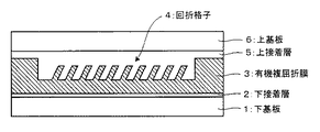
図1は本発明の実施例を説明するための図である。
同図において符号1は下基板、2は下接着層、3は有機福屈折膜、4は回折格子、5は上接着層、6は上基板をそれぞれ示す。
本実施例の光学素子は、波長660nmのレーザー光用の偏光分離用偏光ホログラム素子である。その構成は、光学的に透明な等方性基板に、BK7基板を用い、この基板上にポリエステル系の有機複屈折膜をエポキシ樹脂系紫外線硬化接着材で接着し、有機複屈折膜上に、ドライエッチングにより矩形回折格子を形成した後、エポキシ樹脂系の紫外線硬化樹脂によるオーバーコート層を充填し、格子の埋め込み、その上部に光学的に透明な等方性基板として、BK7基板を接着した構成となっている。BK7基板の空気との界面には使用する波長に対する反射防止層を設けている。そして、回折格子の格子深さ方向を基板の面に垂直な方向に形成している。
FIG. 1 is a diagram for explaining an embodiment of the present invention.
In the figure,
The optical element of the present embodiment is a polarization separation polarization hologram element for laser light having a wavelength of 660 nm. The optically transparent isotropic substrate uses a BK7 substrate, and a polyester-based organic birefringent film is adhered to the substrate with an epoxy resin-based UV-curing adhesive, on the organic birefringent film, After forming a rectangular diffraction grating by dry etching, filled with an overcoat layer of epoxy resin UV curable resin, embedding the grating, and adhering a BK7 substrate as an optically transparent isotropic substrate above it It has become. An antireflection layer for the wavelength to be used is provided on the interface of the BK7 substrate with air. The grating depth direction of the diffraction grating is formed in a direction perpendicular to the surface of the substrate.
次に各構成の詳細について説明する。
作製方法は、初めに、直径100mm、厚さ1.00mmのショット社製光学ガラスBK7からなる下基板1を図示しない回転塗布装置の基板固定テーブルに載せ、真空吸着し、固定した。その後、基板固定テーブルを50rpmで回転させながら、基板の中央部にディスペンサーを用いて屈折率1.52、粘度500cps(25℃)のオーテックス社製EX1500−4エポキシ系紫外線硬化型接着剤を約10g滴下した。その後、基板固定テーブルを最大500rpmで回転させ、基板全面に接着剤を広げ、基板固定テーブルの回転を停止した。
Next, details of each component will be described.
First, the
その後、異常光線方向が、約1.579、常光線方向が約1.670の屈折率を有する厚さ100μmの有機複屈折膜3を、サークルカッターにより直径80mmに切断し、有機複屈折膜3の中心と基板中心とを合わせ載置装置を用いて下基板上の接着剤面に載せた。切断にはサークルカッターの他に、ビク型、ピナクル型、プレス等の方法が使用可能である。
その後、基板固定テーブルを最大2000rpmで回転させ、紫外線硬化型接着剤を振り切り、接着層厚さを基板面内で一定にして有機複屈折膜表面を平坦化した。
基板固定テーブルの回転を停止し、有機複屈折膜側から高圧水銀灯を用いて波長356nm、強度50mW/cm2の紫外線を200秒間照射し、紫外線硬化型接着剤を硬化させ下接着層2を形成した。このときの硬化後の接着厚みは20μmであった。
Thereafter, the organic
Thereafter, the substrate fixing table was rotated at a maximum of 2000 rpm, the ultraviolet curable adhesive was shaken off, and the surface of the organic birefringent film was flattened with the adhesive layer thickness kept constant within the substrate surface.
The rotation of the substrate fixing table is stopped, and an ultraviolet ray having a wavelength of 356 nm and an intensity of 50 mW / cm 2 is irradiated for 200 seconds from the organic birefringent film side using a high pressure mercury lamp to cure the ultraviolet curable adhesive and form the lower
次に、有機複屈折膜3を接着した下基板1を基板固定テーブルから外し、有機複屈折膜3上にポジレジストを1.1μmの厚さに塗布し、90℃30分のプリベークを行った。その後、下基板1を縮小投影露光装置(NA=0.45、σ=0.6、波長;i線)に装着し、1000周期ある回折格子で、Duty約0.5、格子のピッチが2.0μmのデバイスパターンと、位置合わせのためのアライメントマークを設ける2個のアライメントエリア1aの中に、上下基板アライメント用マーク1bとして幅30μm、長さ130μmの十字形状アライメントパターンを基板の赤道上でオリエンテーションフラットに平行方向に基板の中心から±40mmの位置に設け、移動量設定アライメントマーク1cとして各アライメントパターンを中心に52.5μmピッチで+側に2個、−側に2個設置したレチクルを用いて露光を行った後、現像液NMD−3を用いて現像を行い、100℃30分のポストベークを行い、周期的なレジストパターンを完成させた。その後、前記のレジストパターン上にスパッタ法によってAlを蒸着し、引き続きアセトンを用いてレジストを溶解してAlのリフトオフを行い、レジストパターンを反転させたAlパターンを完成させた。
Next, the
図2は回折格子形成段階の1素子分の断面を示す図である。
図3は素子アレイの概要を示す図である。
図3において符号10は素子アレイを示す。
その後、日本真空技術社製NLD−800エッチング装置を用い基板バイアス200W、アンテナ電力1KW、酸素ガス40SCCM、基板温度−30℃のエッチング条件で、前記のAlパターンを金属マスクにして深さを4.0μmまで有機複屈折膜3をエッチングした。このときの回折格子4は基板に垂直に形成されている。回折格子4の断面は図2のようになっている。以後の工程でこの回折格子を一方向に傾斜させる。
その後、リン酸系のAlエッチング液を用いてAlパターンを除去し、1000周期ある凹凸格子(以後回折格子4と記述)と凹凸形状のアライメントマーク1b、1cとを完成させた。以下、素子アレイ10と称する。
FIG. 2 is a diagram showing a cross section for one element in the stage of forming a diffraction grating.
FIG. 3 is a diagram showing an outline of the element array.
In FIG. 3, reference numeral 10 denotes an element array.
After that, using an NLD-800 etching apparatus manufactured by Nippon Vacuum Technology Co., Ltd. under a substrate bias of 200 W, an antenna power of 1 KW, an oxygen gas of 40 SCCM, and a substrate temperature of −30 ° C., the depth is set to 4. The organic
Thereafter, the Al pattern was removed using a phosphoric acid-based Al etching solution to complete a 1000-period uneven grating (hereinafter referred to as diffraction grating 4) and uneven alignment marks 1b, 1c. Hereinafter, the element array 10 is referred to.
図4は上基板の概要を示す図である。
一方の直径100mm、厚さ1.00mmのショット社製BK−7からなる光学ガラスも同様に、光学ガラス上にポジレジストを1.1μmの厚さに塗布し、90℃30分のプリベークを行った。
その後、光学ガラスを縮小投影露光装置(NA=0.45、σ=0.6、波長;i線)に装着し、上下基板アライメント用マーク6bとしてライン幅20μm、長さ110μmの十字形状アライメントパターンを基板の赤道上でオリエンテーションフラットに平行方向に基板の中心から±40mmの位置に設け、移動量設定アライメントマーク6cとして各アライメントパターンを中心に52.5μmピッチで+側に2個、−側に2個設置したレチクルを用いて露光を行った後、現像液NMD−3を用いて現像を行い、100℃30分のポストベークを行い、レジストパターンを完成させた。以下、上基板6とする。
反射防止層としては、MgF/TiO2/SiO2を使用した多層膜によって構成している。
FIG. 4 is a diagram showing an outline of the upper substrate.
Similarly, for the optical glass made of BK-7 manufactured by SCHOTT with a diameter of 100 mm and a thickness of 1.00 mm, a positive resist is applied to the optical glass to a thickness of 1.1 μm and prebaked at 90 ° C. for 30 minutes. It was.
Thereafter, optical glass is mounted on a reduction projection exposure apparatus (NA = 0.45, σ = 0.6, wavelength; i-line), and a cross-shaped alignment pattern having a line width of 20 μm and a length of 110 μm as upper and lower substrate alignment marks 6b. On the equator of the substrate in a direction parallel to the orientation flat at a position of ± 40 mm from the center of the substrate, and as movement amount setting alignment marks 6c, 2 pieces on the + side and 5 on the + side at a 52.5 μm pitch centering on each alignment pattern After exposure using two reticles installed, development was performed using a developer NMD-3, and post-baking was performed at 100 ° C. for 30 minutes to complete a resist pattern. Hereinafter, the
The antireflection layer is composed of a multilayer film using MgF / TiO2 / SiO2.
図5はアライメント接着装置の概要を示す図である。
同図において符号100はアライメント接着装置、101はベース、102はステージ移動装置、103はZ軸移動制御装置、104はX、Y,θ移動ステージを兼ねた下基板チャック、105は石英ガラスマスクホルダ、106は基板吸着用溝、107は真空排気口、108はアライメント検出光学系、109はアライメント光、110は光照射装置をそれぞれ示す。
同図に示すアライメント接着装置100を用いて、前述した素子アレイ10と、上基板6とを対向させて接着する工程を説明する。
同図に示すように、前述した方法で作った上基板6を石英ガラスマスクホルダ105に真空吸着により固定する。次に、複数の回折格子4を形成した素子アレイ7を下基板チャック104上に載置し、真空吸着により固定した後、下基板チャック104と石英ガラスマスクホルダ105間に、φ5mm、高さ5.000mm、平行度0.001mm、表面粗さRa<10nmのジルコニア円柱(図示せず)を支持アームの移動により120°等分の位置に3個挿入した。その後、Z軸制御装置103によりベース101を上昇し、ジルコニア円柱を挟み込み、1N/個で加圧、停止した点をギャップ5.000mmおよび平行面として記憶した。その後、ベース101を下降し、ジルコニア円柱を基板外へ移動した。
次に、素子アレイ7を図で左の方向に押し出し、素子アレイ7の中央に図示しないディスペンサー(接着剤滴下装置)を用い、紫外線硬化型のエポキシ樹脂系接着材7、オーテックス社製EXGT1500−4Kを0.5mL滴下する。この接着剤7は波長365nm、光強度20mW/cm2以上の紫外線で重合・硬化させ、積算光量9000mjで99%重合する接着剤である。
FIG. 5 is a diagram showing an outline of the alignment bonding apparatus.
In the figure, reference numeral 100 is an alignment bonding apparatus, 101 is a base, 102 is a stage moving apparatus, 103 is a Z axis movement control apparatus, 104 is a lower substrate chuck that also serves as an X, Y, and θ moving stage, and 105 is a quartz glass mask holder , 106 is a substrate suction groove, 107 is a vacuum exhaust port, 108 is an alignment detection optical system, 109 is alignment light, and 110 is a light irradiation device.
A process of bonding the element array 10 and the
As shown in the figure, the
Next, the element array 7 is pushed out in the left direction in the figure, and a dispenser (adhesive dripping device) (not shown) is used at the center of the element array 7, an ultraviolet curable epoxy resin adhesive 7, EXGT1500- manufactured by Otex. 4 mL of 4K is added dropwise. This adhesive 7 is an adhesive that is polymerized and cured by ultraviolet rays having a wavelength of 365 nm and a light intensity of 20 mW / cm 2 or more, and is 99% polymerized with an integrated light amount of 9000 mj.
図6は上下各基板のアライメントマークそれぞれと、重ね合わせの状態を示す図である。
素子アレイ10を図で右の方向に戻し、接着層厚み100μm以上を確保するギャップ2.300mmまでZ軸制御装置103によりベース101を上昇した。次に、アライメント検出光学系(画像記憶装置付顕微鏡)108により上下基板のアライメントマーク位置検出を石英ガラスマスクホルダ105を通して行った。アライメント手順は次のとおりである。
はじめに、上基板6のアライメント用マーク6bを検出し、十字線で挟み込んだ画像を記憶し、次に、顕微鏡の焦点位置を下基板1上面付近に合わせ有機複屈折膜3上のアライメント用マーク1bを検出し、検出されたアライメントエラー(画像を記憶した十字線とのズレ)をステージ駆動装置102により、下部基板チャック104をX、Y、θ移動させる事により補正した。これを基板面内で同一線上の80mm離れた少なくとも2点でアライメントを実施した。アライメント補正後、下基板チャック104はベース101に真空吸着等により固定される。ここで上下基板の位置合わせができた。
その後、最終接着剤厚み50μmを確保するため、再度、ベース101を上昇し、接着剤7を基板全体に押し広げ、ギャップ2.200mmの位置で固定した。このとき、上下基板総厚み2.000mm、有機複屈折膜3の厚みが0.100mm、下基板1と有機複屈折膜3の間の下接着層2の厚みが0.050mm、有機複屈折膜3と上基板6の間の上接着層5の厚みが0.050mmとなる。
FIG. 6 is a diagram showing the alignment state of the alignment marks on the upper and lower substrates.
The element array 10 was returned to the right in the figure, and the base 101 was raised by the Z-axis control device 103 to a gap of 2.300 mm to ensure an adhesive layer thickness of 100 μm or more. Next, alignment mark position detection of the upper and lower substrates was performed through the quartz glass mask holder 105 by the alignment detection optical system (microscope with image storage device) 108. The alignment procedure is as follows.
First, the alignment mark 6b on the
Thereafter, in order to secure a final adhesive thickness of 50 μm, the base 101 was raised again, the adhesive 7 was spread over the entire substrate, and fixed at a position of a gap of 2.200 mm. At this time, the total thickness of the upper and lower substrates is 2.000 mm, the thickness of the organic
図7は素子1個分の断面を示す図である。
図8は接着剤の半硬化時点の状態を説明するための図である。
接着剤の広がりが十分行われる間、この状態を2分間保持した。次に、光照射装置110により、石英ガラスマスクホルダ105を通して回折格子4上部と格子溝の接着剤7面に波長365nm、光強度20mW/cm2の紫外線を50秒間照射(エネルギー量E1とする)し、接着剤7を半硬化した。これにより、接着剤7の硬化度が回折格子溝底部が最も小さく、上基板との接触面が硬化度が最も大きい状態の半硬化状態となる。照射時間は最大200秒くらいまではかけることができる。
FIG. 7 is a view showing a cross section of one element.
FIG. 8 is a diagram for explaining the state of the adhesive when it is semi-cured.
This state was maintained for 2 minutes while the adhesive spread sufficiently. Next, the light irradiation device 110, wavelength 365nm to the adhesive surface 7 of the diffraction grating 4 top and grating groove through a quartz glass mask holder 105, (the amount of energy E1) ultraviolet irradiation for 50 seconds the
図9は半硬化状態で上下基板をずらす様子を示す図である。
その後、上下基板に設けた、平行移動量を示すマークを検出し、所定の移動量のマークまでステージ移動装置102により下基板チャック104を移動し、平行移動のためのアライメントを実施した後、下部基板チャック104をベース101に真空吸着により固定した。分かりやすくするためマーク1個分移動した例を同図に示す。これにより、半硬化した接着剤7を通して、有機複屈折膜3にせん断力が働き回折格子4が傾き、保持される。その後、接着剤7全面に波長365nm、光強度20mW/cm2の紫外線を400秒間照射(エネルギー量E2)し、接着剤を硬化して偏光ホログラムアレイ20を完成させた。照射時間は1回目の照射時間とも関係し、最小は250秒くらいまで可能である。
今回、回折格子の傾斜角を6度にするため、素子アレイ10の移動量を105μmとした。なお、移動量は回折格子の倒れ角と有機複屈折膜上のマークと上基板上のマーク間距離により求めた。また、このように、紫外光照射を2段階に分け、接着剤の硬化度合いを制御し、接着剤が弾性を有した状態で外力を加えているため、接着剤に歪が発生するのを防止している。なお、エネルギー量はE1<E2となるよう設定する。
また、本アライメント接着装置100は接着面間の平行度を高精度に維持した状態で平行移動が可能なため、品質の高い加工が可能である。
FIG. 9 shows how the upper and lower substrates are shifted in a semi-cured state.
Thereafter, a mark indicating the amount of parallel movement provided on the upper and lower substrates is detected, the lower substrate chuck 104 is moved by the stage moving device 102 to the mark of a predetermined amount of movement, and alignment for parallel movement is performed. The substrate chuck 104 was fixed to the base 101 by vacuum suction. For the sake of clarity, an example of movement by one mark is shown in the figure. Thereby, the shearing force acts on the organic
This time, in order to set the tilt angle of the diffraction grating to 6 degrees, the movement amount of the element array 10 is set to 105 μm. The amount of movement was determined from the tilt angle of the diffraction grating and the distance between the mark on the organic birefringent film and the mark on the upper substrate. In addition, as described above, ultraviolet light irradiation is divided into two stages, the degree of cure of the adhesive is controlled, and external force is applied while the adhesive has elasticity, thus preventing distortion of the adhesive. is doing. The energy amount is set so that E1 <E2.
In addition, since the alignment bonding apparatus 100 can perform parallel movement while maintaining the parallelism between bonding surfaces with high accuracy, high-quality processing is possible.
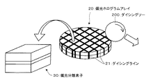
図10は偏光ホログラムアレイの素子単体への分割を説明するための図である。
同図において符号20は偏光ホログラムアレイ、30は偏光ホログラム素子、200はダイシング装置をそれぞれ示す。
その後, 石英ガラスマスクホルダ105の真空吸着を切り、上基板6の真空吸着固定を解除する。次にZ軸制御装置103によりベース101を下降した後、下基板チャック104の真空吸着を切りアライメント接着した偏光ホログラムアレイ20を取り出し、ダイシング装置200により5mm□に切断し、偏光ホログラム素子(偏光分離素子)30とした。
完成した偏光ホログラムの断面は図1に示すとおりである。
FIG. 10 is a diagram for explaining the division of the polarization hologram array into single elements.
In the figure,
Thereafter, the vacuum suction of the quartz glass mask holder 105 is turned off, and the vacuum suction fixation of the
The cross section of the completed polarization hologram is as shown in FIG.
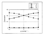
図11は偏光ホログラム素子の回折特性を示す図である。
図7に示すような矩形の回折格子の場合には、レーザー光を垂直入射させた場合には、約40%の回折効率が得られる。このような素子を光ピックアップなどの偏光分離素子に使用する場合には、受光素子には片側の回折光のみを用いることになるため、もう片側の回折光は使用しない。つまり、片側の回折効率のみを向上させることができれば、受光効率が上がることになる。
本実施例のように、回折格子面に対して回折格子ストライプ方向(回折光発生方向)に入射光を傾けた場合の、傾斜角に対する回折効率を同図に示す(実測値)。レーザーの入射角度を変化させることによって、±1次光の回折効率に偏りを設けることが可能なことがわかる。第一実施例においては、回折格子形成方向を6°傾け、実質的にレーザー入射光が6°傾いた構成としているため、回折効率が、+1次で約50%とすることができた。これによってレーザー光の利用効率が上がることになる。また、この時0次回折光の上昇が懸念されるが、同図に示すように、ほぼ増加は見られない。一方、格子内に上記構成のオーバーコート材料を充填しているため、偏光を90°回転させたレーザー光においては、約99%の透過率を示している。
FIG. 11 is a diagram showing diffraction characteristics of the polarization hologram element.
In the case of a rectangular diffraction grating as shown in FIG. 7, when the laser beam is vertically incident, a diffraction efficiency of about 40% can be obtained. When such an element is used for a polarization separation element such as an optical pickup, only the diffracted light on one side is used for the light receiving element, so the diffracted light on the other side is not used. That is, if only the diffraction efficiency on one side can be improved, the light receiving efficiency will increase.
The diffraction efficiency with respect to the tilt angle when the incident light is tilted in the diffraction grating stripe direction (diffracted light generation direction) with respect to the diffraction grating surface as in this embodiment is shown in the figure (actual measurement value). It can be seen that a deviation can be provided in the diffraction efficiency of ± first-order light by changing the incident angle of the laser. In the first embodiment, the diffraction grating formation direction is inclined by 6 ° and the laser incident light is substantially inclined by 6 °, so that the diffraction efficiency can be about 50% in the + 1st order. This increases the utilization efficiency of the laser beam. At this time, there is a concern about the rise of the 0th-order diffracted light, but almost no increase is seen as shown in FIG. On the other hand, since the overcoat material having the above-described configuration is filled in the grating, the laser beam obtained by rotating the polarized light by 90 ° shows a transmittance of about 99%.
本実施例においては、回折格子の形成方向を基板面から傾けて形成することにより、使用する回折光の回折効率を向上することができた。また、格子内をオーバーコート材料としての接着剤で充填し、その屈折率を複屈折材料とマッチングさせることにより、偏光分離素子の特性を低下することなく充填と接着ができている。紫外線硬化型接着剤を用いているので、プロセスが容易であり、また、プロセスの時間短縮が可能となった。
また、異方性膜に延伸された高分子有機膜を使用することにより、より低価格での素子作製が可能である。また、回折格子面の上方に光学的に平滑なBK7基板を接着することにより、波面収差特性の低下が防止できた。
オーバーコート層により接着することにより、樹脂の共通化を図ることができ、コストも低減できる。また、素子表面に使用波長に対する無反射コーティングを施すことにより、透過率、回折効率などの特性が向上する。また、回折格子の形成方法に関しても、より容易な方法で所望の形状が形成できるため、容易に作製可能となる。
In this example, the diffraction efficiency of the diffracted light used could be improved by tilting the formation direction of the diffraction grating from the substrate surface. In addition, by filling the inside of the grating with an adhesive as an overcoat material and matching the refractive index with the birefringent material, filling and bonding can be performed without degrading the characteristics of the polarization separation element. Since an ultraviolet curable adhesive is used, the process is easy and the process time can be shortened.
Further, by using a polymer organic film stretched on an anisotropic film, it is possible to fabricate a device at a lower price. Further, by adhering an optically smooth BK7 substrate above the diffraction grating surface, it was possible to prevent the wavefront aberration characteristic from being deteriorated.
By bonding with the overcoat layer, the resin can be shared and the cost can be reduced. In addition, by applying a non-reflective coating for the wavelength used to the element surface, characteristics such as transmittance and diffraction efficiency are improved. Also, with respect to the method of forming the diffraction grating, since a desired shape can be formed by an easier method, it can be easily manufactured.
図12は本発明の他の実施例を説明するための図である。
同図において符号8は4分の1波長板(λ/4板と表記する)、9は粘着剤をそれぞれ示す。
本実施例による偏光分離素子は波長660nmのレーザー光に対する偏光ホログラム素子である。本実施例の構成は光学的に透明な等方性基板として、BK7基板上にアクリル系紫外線硬化接着材による接着層を介し、ポリエステル系有機材料を延伸し作製した有機複屈折膜を形成した基板上に、矩形回折格子を形成し、その上部に格子を埋め込む様にエポキシ系の紫外線硬化樹脂によるオーバーコート層を形成し、その上部にBK7基板にλ/4板を形成した光学的に透明な等方性基板を構成している。
FIG. 12 is a diagram for explaining another embodiment of the present invention.
In the figure,
The polarization separation element according to this embodiment is a polarization hologram element for laser light having a wavelength of 660 nm. The configuration of this example is an optically transparent isotropic substrate, a substrate on which an organic birefringent film formed by stretching a polyester organic material on a BK7 substrate through an adhesive layer made of an acrylic ultraviolet curable adhesive is formed. On top of this, a rectangular diffraction grating is formed, an overcoat layer made of an epoxy-based ultraviolet curable resin is formed so as to embed the grating on the top, and a λ / 4 plate is formed on the BK7 substrate, which is optically transparent. An isotropic substrate is formed.
また、BK7基板の空気との界面に使用する波長に対する反射防止層を設けている。また、ここで回折格子の格子形成方向を図1に示すように、基板と垂直な面から角度をつけて形成している。その角度としては、4°の傾きを持たせている。
偏光ホログラム素子の作製方法は、初めに、直径100mm、厚さ1.00mmのショット社製光学ガラスBK7からなる下基板を図示しない回転塗布装置の基板固定テーブルに載せ、真空吸着し、固定した。その後、基板固定テーブルを平均30rpmで回転させながら、下基板の中央部にディスペンサーを用いて屈折率1.52、粘度500cps(25℃)のスリーボンド社製TB3042アクリル系紫外線硬化型接着剤を約10g滴下した。その後、基板固定テーブルを約400rpmで回転させ、下基板全面に接着剤を広げ、基板固定テーブルの回転を停止した。
In addition, an antireflection layer for the wavelength used at the interface with the air of the BK7 substrate is provided. Here, the diffraction grating is formed at an angle from a plane perpendicular to the substrate, as shown in FIG. The angle is 4 °.
In the method of manufacturing the polarization hologram element, first, a lower substrate made of optical glass BK7 made by SCHOTT having a diameter of 100 mm and a thickness of 1.00 mm was placed on a substrate fixing table of a spin coater (not shown), and vacuum-adsorbed and fixed. Thereafter, while rotating the substrate fixing table at an average of 30 rpm, about 10 g of TB3042 acrylic UV curable adhesive manufactured by ThreeBond Co., Ltd. having a refractive index of 1.52 and a viscosity of 500 cps (25 ° C.) using a dispenser at the center of the lower substrate. It was dripped. Thereafter, the substrate fixing table was rotated at about 400 rpm, the adhesive was spread over the entire lower substrate, and the rotation of the substrate fixing table was stopped.
その後、異常光線方向が、約1.579、常光線方向が約1.670の屈折率を有する厚さ100μmの有機複屈折膜を、サークルカッターにより直径80mmに切断し、有機複屈折膜の中心と光学ガラス基板中心とを合わせ載置装置を用いて下基板上の接着剤面に載せた。
その後、基板固定テーブルを最大2000rpmで回転させ、紫外線硬化型接着剤を振り切り、接着層厚さを光学ガラス面内で一定にして有機複屈折膜表面を平坦化した。
その後、基板固定テーブルの回転を停止し、有機複屈折膜側から高圧水銀灯を用いて波長356nm、強度40mW/cm2の紫外線を250秒間照射し、紫外線硬化型接着剤を硬化した。
このときの硬化後の接着厚みは20μmであった。
Thereafter, an organic birefringent film having a refractive index of about 1.579 for the extraordinary ray direction and about 1.670 for the ordinary ray direction is cut to a diameter of 80 mm with a circle cutter, and the center of the organic birefringent film is cut. And the center of the optical glass substrate were placed on the adhesive surface on the lower substrate using a mounting device.
Thereafter, the substrate fixing table was rotated at a maximum of 2000 rpm, the ultraviolet curable adhesive was shaken off, and the surface of the organic birefringent film was flattened with the adhesive layer thickness kept constant within the optical glass surface.
Thereafter, the rotation of the substrate fixing table was stopped, and ultraviolet rays having a wavelength of 356 nm and an intensity of 40 mW / cm 2 were irradiated for 250 seconds from the organic birefringent film side using a high-pressure mercury lamp to cure the ultraviolet curable adhesive.
The adhesive thickness after curing at this time was 20 μm.
次に、有機複屈折膜を接着した基板を基板固定テーブルから外し、有機複屈折膜上にポジレジストを1.1μmの厚さに塗布し、90℃30分のプリベークを行った。その後、下基板を縮小投影露光装置(NA=0.45、σ=0.6、波長;i線)に装着し、1000周期ある回折格子はDuty約0.5、格子のピッチが2.0μmのデバイスパターンと幅30μm、長さ130μmの十字形状アライメントパターンを光学ガラス基板の赤道上でオリエンテーションフラットに平行方向に光学ガラス基板の中心から±40mmの位置に設け、各アライメントパターンを中心に52.5μmピッチでそれぞれ+側に2個、−側に2個設置したレチクルを用いて露光を行った。その後、現像液NMD−3を用いて現像を行い、100℃30分のポストベークを行い、周期的なレジストパターンを完成させた。その後、前記のレジストパターン上にスパッタ法によってAlを蒸着し、引き続きアセトンを用いてレジストを溶解してAlのリフトオフを行い、レジストパターンを反転させたAlパターンを完成させた。
その後、日本真空技術社製NLD−800エッチング装置を用い、基板バイアス200W、アンテナ電力1KW、酸素ガス40SCCM、基板温度−30℃のエッチング条件で、前記のAlパターンを金属マスクにして有機複屈折膜の深さを4.0μmまでエッチングした。このときの回折格子は光学ガラス基板に垂直に形成されている。
その後、リン酸系のAlエッチング液を用いてAlパターンを除去し、1000周期ある凹凸格子(以後回折格子と記述)と凹凸形状のアライメントマークとを完成させた。以下、素子アレイとする。
Next, the substrate to which the organic birefringent film was bonded was removed from the substrate fixing table, a positive resist was applied to the organic birefringent film to a thickness of 1.1 μm, and prebaked at 90 ° C. for 30 minutes. Thereafter, the lower substrate is mounted on a reduction projection exposure apparatus (NA = 0.45, σ = 0.6, wavelength; i-line), a diffraction grating having 1000 periods has a duty of about 0.5, and the pitch of the grating is 2.0 μm. A device pattern and a cross-shaped alignment pattern having a width of 30 μm and a length of 130 μm are provided on the equator of the optical glass substrate in a direction parallel to the orientation flat at a position of ± 40 mm from the center of the optical glass substrate. Exposure was performed using two reticles provided on the positive side and two on the negative side at a pitch of 5 μm. Thereafter, development was performed using a developer NMD-3, and post-baking was performed at 100 ° C. for 30 minutes to complete a periodic resist pattern. Thereafter, Al was vapor-deposited on the resist pattern by sputtering, and subsequently the resist was dissolved using acetone to lift off Al, thereby completing an Al pattern in which the resist pattern was inverted.
Then, using an NLD-800 etching apparatus manufactured by Nippon Vacuum Engineering Co., Ltd., an organic birefringent film using the Al pattern as a metal mask under the etching conditions of substrate bias 200 W,
Thereafter, the Al pattern was removed using a phosphoric Al etching solution to complete a concavo-convex grating having 1000 cycles (hereinafter referred to as a diffraction grating) and a concavo-convex alignment mark. Hereinafter, an element array is used.
図13はλ/4板の貼り付け位置関係を説明するための図である。
一方の直径100mm、厚さ1.00mmのショット社製BK−7からなる光学ガラスも同様に、光学ガラス上にポジレジストを1.1μmの厚さに塗布し、90℃30分のプリベークを行った。その後、光学ガラスを縮小投影露光装置(NA=0.45、σ=0.6、波長;i線)に装着し、2ヵ所のアライメントマークエリア6aに、ライン幅20μm、長さ110μmの十字形状アライメントパターン6bのレチクルを用いて露光を行った後、現像液NMD−3を用いて現像を行い、100℃30分のポストベークを行い、レジストパターンを完成させた。以下、上基板6とする。
この上に、フィルムラミネータ装置を用い、ポリエステル系の位相差膜よりなる膜厚約100μmの片面粘着材9付きλ/4板8の位相軸8aを上基板十字形状アライメントパターンの配置方向に対し、45度ずらし貼り付け、光学的に透明な等方性基板とした。以下、上カバー11と記述する。λ/4板8貼り付けは十字形状アライメントマークの反対面とした。
なお、λ/4板貼り付け面の反対面にはMgF/TiO2/SiO2構成の多層膜の反射防止層(図示省略)を形成している。
FIG. 13 is a diagram for explaining the positional relationship between the λ / 4 plates.
Similarly, for the optical glass made of BK-7 manufactured by SCHOTT with a diameter of 100 mm and a thickness of 1.00 mm, a positive resist is applied to the optical glass to a thickness of 1.1 μm and prebaked at 90 ° C. for 30 minutes. It was. Thereafter, the optical glass is mounted on a reduction projection exposure apparatus (NA = 0.45, σ = 0.6, wavelength; i-line), and two
On top of this, using a film laminator apparatus, the phase axis 8a of the λ / 4
A multilayer antireflection layer (not shown) having a MgF / TiO2 / SiO2 structure is formed on the surface opposite to the λ / 4 plate attachment surface.
前述した方法で作った上カバー11をλ/4板8の貼り付け面を下向きにして真空吸着により石英ガラスマスクホルダ105に固定し、次に、回折格子4を形成した素子アレイ10を下基板チャック104上に載置し、真空吸着により固定した。その後、下基板チャック104と石英ガラスマスクホルダ105間に、φ5mm、高さ5.000mm、平行度0.001mm、表面粗さRa<10nmのジルコニア円柱を支持アームの移動により120°等分の位置に3個挿入した後、Z軸制御装置103によりベース101を上昇し、ジルコニア円柱を挟み込み、1N/個で加圧、停止した点をギャップ5.000mmおよび平行面として記憶した後、ベース101を下降し、ジルコニア円柱を基板外へ移動した。
次に、素子アレイ10を図で左の方向に押し出し、素子アレイ10の中央に図示しないディスペンサーを用い、紫外線硬化型のエポキシ樹脂系接着剤7、オーテックス社製EXGT1500−4Kを0.5mL滴下する。この接着剤7は波長365nm、光強度20mW/cm2以上の紫外線で重合し、積算光量9000mjで99%重合する接着剤である。
The upper cover 11 made by the above-described method is fixed to the quartz glass mask holder 105 by vacuum suction with the surface to which the λ / 4
Next, the element array 10 is pushed out in the left direction in the figure, and a 0.5 mL drop of UV curable epoxy resin adhesive 7, EXGT1500-4K manufactured by Otex Co., Ltd. is dropped at the center of the element array 10 using a dispenser (not shown). To do. This adhesive 7 is an adhesive that is polymerized by ultraviolet rays having a wavelength of 365 nm and a light intensity of 20 mW / cm 2 or more, and is 99% polymerized with an integrated light amount of 9000 mj.
次に, 素子アレイ10を図で右の方向に戻し、接着層厚み100μm以上を確保するギャップまでベース101を上昇した。次に、上下基板のアライメントマーク位置検出を,石英ガラスマスクホルダ105を通してアライメント検出光学系108によりアライメントを行った。はじめに、上基板6のアライメントマークを検出し、十字線で挟み込んだ画像を記憶し、次に、顕微鏡の焦点位置を下基板1に合わせ下基板のアライメントマークを検出し、検出されたアライメントエラー(画像を記憶した十字線とのズレ)をステージ移動装置102により、下部基板チャック104をX、Y、θ移動させる事により補正した。これを基板面内で同一線上の80mm離れた少なくとも2点でアライメントを実施した。アライメント補正後、下部基板チャック104はベース101に真空吸着等で固定した。その後、最終接着剤厚み50μmを確保するため、再度、ベース101を上昇し、接着剤を基板全体に押し広げ、ギャップ2.200mmの位置で固定した。
Next, the element array 10 was returned to the right in the figure, and the base 101 was raised to a gap that secures an adhesive layer thickness of 100 μm or more. Next, alignment mark position detection on the upper and lower substrates was performed by the alignment detection optical system 108 through the quartz glass mask holder 105. First, the alignment mark on the
接着剤の広がりが十分行われる間、この状態を2分間保持した。次に、光照射装置により、石英ガラスマスクホルダ105を通し、図示しない遮光マスクを用い、回折格子上部と格子溝の接着剤面にのみ波長365nm、光強度20mW/cm2の紫外線を100秒照射(E1)し、接着剤を半硬化した。これにより、接着剤の硬化度が回折格子溝底部が最も小さく、上基板との接触面が最も大きい状態の半硬化状態とした。
その後、上下基板に設けた、平行移動量を示すマークを検出し、下部基板チャック104を所定の移動量のマークまでステージ駆動装置102により、平行移動のためのアライメントを実施した後、下部基板チャックをベース101に真空吸着により固定した。これにより、半硬化した接着剤とともに、有機複屈折膜に平行方向の力が働きこれにより、回折格子が傾く。その後、接着剤全面に波長365nm、光強度20mW/cm2の紫外線を400秒間照射(E2:E2>E1)し、接着剤を完全硬化した。今回、回折格子の傾斜角を4°にするため、素子アレイ10の移動量を61μmとした。なお、移動量は回折格子の倒れ角と有機複屈折膜上のマークと上基板6上のマーク間距離により求めた。
This state was maintained for 2 minutes while the adhesive spread sufficiently. Next, with a light irradiation device, ultraviolet light having a wavelength of 365 nm and a light intensity of 20 mW / cm 2 is irradiated for 100 seconds only on the upper surface of the diffraction grating and the adhesive surface of the grating groove through a quartz glass mask holder 105 and using a light shielding mask (not shown). (E1) and the adhesive was semi-cured. As a result, the adhesive was cured in a semi-cured state where the diffraction grating groove bottom was the smallest and the contact surface with the upper substrate was the largest.
After that, a mark indicating the amount of parallel movement provided on the upper and lower substrates is detected, and the lower substrate chuck 104 is aligned for parallel movement by the stage driving device 102 up to the mark of the predetermined amount of movement. Was fixed to the base 101 by vacuum adsorption. As a result, a force in a parallel direction acts on the organic birefringent film together with the semi-cured adhesive, thereby tilting the diffraction grating. Then, wavelength 365nm to the adhesive over the entire surface, ultraviolet irradiation for 400 seconds of light intensity 20mW / cm 2 (E2: E2 > E1) , and completely cure the adhesive. In this case, in order to set the tilt angle of the diffraction grating to 4 °, the movement amount of the element array 10 is set to 61 μm. The amount of movement was determined from the tilt angle of the diffraction grating and the distance between the mark on the organic birefringent film and the mark on the
その後、石英ガラスマスクホルダ105の真空吸着を切り、上基板6の真空吸着固定を解除する。次にZ軸制御装置によりベース101を下降した後、下基板チャック104の真空吸着を切り、アライメント接着した偏光ホログラムアレイ40を取り出し、ダイシング装置200により5mm□に切断し、偏光ホログラム素子50とした。
接着層には界面での反射を極力避けるために、BK7基板に屈折率を一致させた紫外線硬化接着剤を使用している。また、オーバーコート層(上接着層)の屈折率をほぼ有機複屈折膜の異常光線方向の屈折率と合せた材料を使用している。
Thereafter, the vacuum suction of the quartz glass mask holder 105 is turned off, and the vacuum suction fixation of the
In order to avoid reflection at the interface as much as possible, an ultraviolet curing adhesive having a refractive index matched to that of the BK7 substrate is used for the adhesive layer. In addition, a material in which the refractive index of the overcoat layer (upper adhesive layer) is substantially matched with the refractive index in the extraordinary ray direction of the organic birefringent film is used.
本実施例による偏光ホログラム素子の回折特性について、図11を用いて詳細に説明する。本実施例においては、回折格子の形成方向を4°傾け、実質的にレーザー入射光を4°傾けた構成としているため、回折効率が、+1次で約48%とすることができた。これによってレーザー光の利用効率が上がることになる。また、この時0次回折光の上昇が懸念されるが、同図に示すように、ほぼ増加は見られない。一方、格子内に上記構成のオーバーコート材料を充填しているため、偏光を90°回転させたレーザー光においては、約99%の透過率を示している。また、λ/4板8を一体で形成しているため、直線偏光を入射させると、円偏光で出射される。この機能によって、光ピックアップのような往復光路を持った光学系において、往復の光路を分離することが可能になる。
尚、本発明における実施例においては、波長は660nmについての素子をあげているが、780nm用、二波長用なども格子深さを変更することで対応可能である。
The diffraction characteristics of the polarization hologram element according to this embodiment will be described in detail with reference to FIG. In this example, the diffraction grating was formed at a tilt angle of 4 ° and the laser incident light was tilted by 4 °, so that the diffraction efficiency was about 48% in the + 1st order. This increases the utilization efficiency of the laser beam. At this time, there is a concern about the rise of the 0th-order diffracted light, but almost no increase is seen as shown in FIG. On the other hand, since the overcoat material having the above-described configuration is filled in the grating, the laser beam obtained by rotating the polarized light by 90 ° shows a transmittance of about 99%. In addition, since the λ / 4
In the embodiment of the present invention, an element with a wavelength of 660 nm is given, but it is possible to change the grating depth for 780 nm and two wavelengths.
図14は本発明の素子を用いる光ピックアップの構成を説明するための図である。
同図において符号300は光ピックアップ、301は光源としてのレーザーダイオード、302はコリメータレンズ、303は対物レンズ、304は受光素子としてのフォトダイオード、Dは光ディスクをそれぞれ示す。
例えばCD用光ピックアップではレーザーダイオードから出射された波長780nmの光は、本発明の偏光分離素子50、コリメータレンズ302、対物レンズ303を通って光ディスクD(この例ではCD)を照射し、CDの記録ピットからの反射光は偏光分離素子50で回折されフォトダイオード304に導かれ、フォーカス検出、トラック検出、信号検出が行われる。
本例の光ピックアップを用い、CD−RWに信号を記録し、その後同じ光ピックアップで信号の再生を行った所、プリズムを接着したビームスプリッタとλ/4波長板を組み合わせた従来のCD用光ピックアップと同等の再生信号出力を得ることができ、本例の光ピックアップが従来の光ピックアップと同等の記録/再生特性を持つことが確認できた。
また本例のピックアップでは、偏光分離素子がプリズムを接着したビームスプリッタよりも小さくなっており、かつ偏光分離素子にλ/4波長板も組み込んでいるため、従来の光ピックアップと比較して小型化が実現できていた。
FIG. 14 is a diagram for explaining the configuration of an optical pickup using the element of the present invention.
In the figure, reference numeral 300 denotes an optical pickup, 301 denotes a laser diode as a light source, 302 denotes a collimator lens, 303 denotes an objective lens, 304 denotes a photodiode as a light receiving element, and D denotes an optical disk.
For example, in a CD optical pickup, light having a wavelength of 780 nm emitted from a laser diode irradiates the optical disc D (CD in this example) through the
When the optical pickup of this example was used to record a signal on a CD-RW, and then the signal was reproduced with the same optical pickup, a conventional CD light combining a beam splitter with a prism attached and a λ / 4 wavelength plate. A reproduction signal output equivalent to that of the pickup could be obtained, and it was confirmed that the optical pickup of this example had recording / reproduction characteristics equivalent to those of the conventional optical pickup.
In addition, in the pickup of this example, the polarization separation element is smaller than the beam splitter to which the prism is bonded, and a λ / 4 wavelength plate is incorporated in the polarization separation element, so it is smaller than the conventional optical pickup. Was realized.
図5を援用して本発明の他の実施例を説明する。
本実施例では接着剤7として熱硬化型の接着剤を用いる。樹脂の種類が異なる点以外の特性や、その他の材質、製法は実施例1と同様である。この場合は、図5における光照射装置110の代わりに、石英ガラスホルダ105に対してほぼ均等に熱を与える熱源(図示せず)を接触させておく。そして、下基板チャックには冷却装置(図示せず)を接触させておく。接着剤の半硬化を行うときは、熱源と冷却装置を同時に作動させ、上基板6から下基板1に向かって所定の温度勾配を所定時間与える。与える温度は、上基板6に接触している熱硬化樹脂が完全硬化するのに必要な温度T0以下になるような温度T1に設定しておく。その結果、上基板6に近い部分は硬化が或る程度進むのに対し、格子の凹部の底の方は僅かな硬化が生ずるだけの、いわゆる半硬化状態を作ることができる。
この半硬化状態で、上基板6を下基板1に対して所定量移動させれば図1に示したような、傾斜した回折格子を作ることができる。その状態を保ったまま、今度は下基板1側の冷却装置は作動させず、上基板6側の熱源から、熱硬化型樹脂の硬化に必要な所定温度T0以上の温度T2を与え、回折格子の凹部の底まで硬化が進むよう、その温度を所定時間保持する。特に図示しないが、冷却装置側に別の熱源を用意しておいて、第2の硬化工程の時は下側からも加熱するようにすることもできる。
完成品は実施例1の場合と全く同等に扱うことができる。
Another embodiment of the present invention will be described with reference to FIG.
In this embodiment, a thermosetting adhesive is used as the adhesive 7. Characteristics other than the difference in the type of resin, other materials, and the manufacturing method are the same as those in the first embodiment. In this case, instead of the light irradiation device 110 in FIG. 5, a heat source (not shown) that applies heat to the quartz glass holder 105 almost uniformly is brought into contact. Then, a cooling device (not shown) is brought into contact with the lower substrate chuck. When semi-curing the adhesive, the heat source and the cooling device are simultaneously operated to give a predetermined temperature gradient from the
If the
The finished product can be handled in exactly the same way as in the first embodiment.
1 下基板
3 有機複屈折膜
4 回折格子
5 上接着層
6 上基板
20 偏光ホログラムアレイ
30 偏光分離素子
1
Claims (12)
前記等方性接着剤により前記上基板を接着する工程は、前記等方性接着剤の上に前記上基板を載置した状態で、1回目の硬化処理をする第1硬化工程と、前記上基板と前記下基板とを相対的に平行移動させる工程と、平行移動後に2回目の硬化処理をする第2硬化工程とを有することを特徴とする偏光ホログラム素子の製造方法。 A step of attaching an organic birefringent film having a different refractive index to a vibrating surface of different incident light on a first transparent substrate (referred to as a lower substrate) , and a periodic concavo-convex grating (hereinafter referred to as diffraction) on the organic birefringent film Forming a grating), filling a concave portion of the diffraction grating with an isotropic adhesive, and bonding a second transparent substrate (referred to as the upper substrate); and the isotropic bonding When the agent is in a semi-cured state, there are a step of applying an external force between the upper substrate and the lower substrate in a direction parallel to both substrate surfaces, and a step of sufficiently curing the isotropic adhesive in that state. And
The step of bonding the upper substrate with the isotropic adhesive includes a first curing step of performing a first curing process in a state where the upper substrate is placed on the isotropic adhesive, and the upper A method for manufacturing a polarization hologram element, comprising: a step of relatively translating a substrate and the lower substrate; and a second curing step of performing a second curing process after the parallel movement .
前記外力は一方の基板に対し、他方の基板を平行移動させ与えることを特徴とする偏光ホログラム素子の製造方法。 In the manufacturing method of the polarization hologram element according to claim 1,
A method of manufacturing a polarization hologram element, wherein the external force is applied to one substrate by translating the other substrate .
前記等方性接着剤は光硬化型接着剤であることを特徴とする偏光ホログラム素子の製造方法。 In the manufacturing method of the polarization hologram element according to claim 1 or 2,
The method of manufacturing a polarization hologram element, wherein the isotropic adhesive is a photocurable adhesive .
前記等方性接着剤はアクリル樹脂系、またはエポキシ樹脂系の紫外線硬化型接着剤であることを特徴とする偏光ホログラム素子の製造方法。 In the manufacturing method of the polarization hologram element according to claim 3,
The method of manufacturing a polarization hologram element, wherein the isotropic adhesive is an acrylic resin-based or epoxy resin-based ultraviolet curable adhesive .
前記第1および第2の硬化工程は、前記等方性接着剤に付与するそれぞれのエネルギーをE1、E2としたとき、
E1≦E2
となるように照射することを特徴とする偏光ホログラム素子の製造方法。 In the manufacturing method of the polarization hologram element according to claim 3 or 4 ,
In the first and second curing steps, when the respective energies applied to the isotropic adhesive are E1 and E2,
E1 ≦ E2
Irradiating so as to obtain a polarization hologram element manufacturing method.
前記等方性接着剤は熱硬化型接着剤であることを特徴とする偏光ホログラム素子の製造方法。 In the manufacturing method of the polarization hologram element according to claim 1 or 2 ,
The method of manufacturing a polarization hologram element, wherein the isotropic adhesive is a thermosetting adhesive .
前記第1および第2の硬化工程は、前記等方性接着剤に付与するそれぞれの温度をT1、T2とし、前記熱硬化型接着剤の硬化温度をT0としたとき、
T1<T0<T2
となるように与えることを特徴とする偏光ホログラム素子の製造方法。 In the manufacturing method of the polarization hologram element according to claim 6,
In the first and second curing steps, when the respective temperatures applied to the isotropic adhesive are T1 and T2, and the curing temperature of the thermosetting adhesive is T0,
T1 <T0 <T2
A method for producing a polarization hologram element, characterized by:
前記第1の硬化工程は、前記上基板の側から所定の温度を与え、前記した下基板の側から冷却することによって、前記熱硬化型接着剤に所定の温度勾配を所定時間与えることを特徴とする偏光ホログラム素子の製造方法。 In the manufacturing method of the polarization hologram element according to claim 7,
In the first curing step, a predetermined temperature gradient is applied to the thermosetting adhesive for a predetermined time by applying a predetermined temperature from the upper substrate side and cooling from the lower substrate side. A manufacturing method of a polarization hologram element.
前記下基板、前記有機複屈折膜、前記上基板のいずれか2つに、平行移動量を検出するためのマークを形成する工程をさらに含み、前記接着工程には、前記マークを検出する検出手段と、前記上基板もしくは下基板の内の一方の基板を保持し固定する固定手段と、他方の基板を保持し、該基板をX座標、Y座標および回転方向に移動可能な移動手段と、前記固定された基板に対し、それに対向させた他方の基板の平行基準を設定する基準設定手段と、接着層厚みを規定する規定手段と、光を照射する光照射手段と、前記等方性接着剤を滴下する滴下手段とを有するアライメント接着装置を用いることを特徴とする偏光ホログラム素子の製造方法。 In the manufacturing method of the polarization hologram element according to any one of claims 1 to 8 ,
The method further includes a step of forming a mark for detecting a parallel movement amount on any two of the lower substrate, the organic birefringent film, and the upper substrate, and the adhering step includes a detecting unit that detects the mark. A fixing unit that holds and fixes one of the upper substrate and the lower substrate, a moving unit that holds the other substrate and can move the substrate in the X-coordinate, the Y-coordinate, and the rotation direction; Reference setting means for setting the parallel reference of the other substrate opposed to the fixed substrate, definition means for specifying the adhesive layer thickness, light irradiation means for irradiating light, and the isotropic adhesive A method of manufacturing a polarization hologram element, comprising using an alignment bonding apparatus having a dropping unit for dropping the liquid .
Priority Applications (1)
| Application Number | Priority Date | Filing Date | Title |
|---|---|---|---|
| JP2004159997A JP4440706B2 (en) | 2004-05-28 | 2004-05-28 | Polarization hologram element, manufacturing method thereof, optical pickup device using polarization hologram element, and optical disc drive apparatus |
Applications Claiming Priority (1)
| Application Number | Priority Date | Filing Date | Title |
|---|---|---|---|
| JP2004159997A JP4440706B2 (en) | 2004-05-28 | 2004-05-28 | Polarization hologram element, manufacturing method thereof, optical pickup device using polarization hologram element, and optical disc drive apparatus |
Publications (2)
| Publication Number | Publication Date |
|---|---|
| JP2005338638A JP2005338638A (en) | 2005-12-08 |
| JP4440706B2 true JP4440706B2 (en) | 2010-03-24 |
Family
ID=35492274
Family Applications (1)
| Application Number | Title | Priority Date | Filing Date |
|---|---|---|---|
| JP2004159997A Expired - Fee Related JP4440706B2 (en) | 2004-05-28 | 2004-05-28 | Polarization hologram element, manufacturing method thereof, optical pickup device using polarization hologram element, and optical disc drive apparatus |
Country Status (1)
| Country | Link |
|---|---|
| JP (1) | JP4440706B2 (en) |
Families Citing this family (5)
| Publication number | Priority date | Publication date | Assignee | Title |
|---|---|---|---|---|
| TWI470561B (en) * | 2005-12-19 | 2015-01-21 | Internat Frontier Tech Lab Inc | The card can be judged by the pictographic chip |
| WO2007108244A1 (en) * | 2006-03-17 | 2007-09-27 | Sharp Kabushiki Kaisha | Display panel, polarization plate to be adhered on such display panel and display device using such display panel and polarization plate |
| WO2007142179A1 (en) * | 2006-06-07 | 2007-12-13 | Konica Minolta Holdings, Inc. | Quarter-wave plate, and optical pickup device |
| CN103576220B (en) * | 2013-10-11 | 2016-01-06 | 中国科学院上海光学精密机械研究所 | Quartz 1 × 2 beam splitting skew ray grid of TE polarization |
| JP7225534B2 (en) * | 2017-01-18 | 2023-02-21 | 大日本印刷株式会社 | Optical element, multi-faceted body of optical element, optical module, and light irradiation device |
-
2004
- 2004-05-28 JP JP2004159997A patent/JP4440706B2/en not_active Expired - Fee Related
Also Published As
| Publication number | Publication date |
|---|---|
| JP2005338638A (en) | 2005-12-08 |
Similar Documents
| Publication | Publication Date | Title |
|---|---|---|
| US20110216255A1 (en) | Polarization diffraction grating, method for manufacturing the same, and optical pickup apparatus using the polarization diffraction grating | |
| JP4440706B2 (en) | Polarization hologram element, manufacturing method thereof, optical pickup device using polarization hologram element, and optical disc drive apparatus | |
| JP3544461B2 (en) | Optical element for optical pickup, method for manufacturing optical element for optical pickup, and optical pickup | |
| US5774443A (en) | Optical head device capable of reducing the light power loss | |
| US20050073747A1 (en) | Diffractive optical element, manufacturing method thereof, optical pickup apparatus and optical disk drive apparatus | |
| JP2002014228A (en) | Phase shifter and optical head device | |
| KR20050091757A (en) | Liquid crystal component | |
| JP2000249831A (en) | Optical device and optical head device | |
| JP2006040424A (en) | Polarization splitting element, optical pickup, optical disk device, and manufacturing method of polarization splitting element | |
| JP4204809B2 (en) | Method for manufacturing diffractive optical element | |
| JP4139140B2 (en) | Polarization hologram element and manufacturing method thereof | |
| JP3947828B2 (en) | Optical head device and manufacturing method thereof | |
| JP4421249B2 (en) | Method for manufacturing polarization separating element | |
| JP4139129B2 (en) | Method for manufacturing polarization separating element, bonding apparatus, and optical pickup apparatus | |
| JP4229709B2 (en) | Method of manufacturing polarization separating element and organic birefringent film bonding apparatus therefor | |
| JP4251606B2 (en) | Polarizing optical element, manufacturing method of polarizing optical element, optical pickup apparatus, and optical disc apparatus | |
| JP4237020B2 (en) | Method for manufacturing polarization separation element | |
| JP3713778B2 (en) | Optical head device | |
| JP4084071B2 (en) | Method for manufacturing polarization separation element, polarization separation element, hologram laser unit, optical pickup | |
| JP2003302527A (en) | Polarized beam splitter and fabricating method thereof, bonding device, and optical pickup unit | |
| JP4222860B2 (en) | Method for producing polarization separating element using organic birefringent film and organic birefringent film bonding apparatus used therefor | |
| JP2005249856A (en) | Alignment joining method, alignment joining device, and optical device | |
| JP2005310236A (en) | Wavelength selective polarization hologram element | |
| JP2003322713A (en) | Diffraction optical element and method of manufacturing the same, optical pickup device and optical disk driving device | |
| JP2002350609A (en) | Method for manufacturing optical element, optical element and optical pickup device |
Legal Events
| Date | Code | Title | Description |
|---|---|---|---|
| A621 | Written request for application examination |
Free format text: JAPANESE INTERMEDIATE CODE: A621 Effective date: 20061218 |
|
| A977 | Report on retrieval |
Free format text: JAPANESE INTERMEDIATE CODE: A971007 Effective date: 20090330 |
|
| A131 | Notification of reasons for refusal |
Free format text: JAPANESE INTERMEDIATE CODE: A131 Effective date: 20090818 |
|
| A521 | Written amendment |
Free format text: JAPANESE INTERMEDIATE CODE: A523 Effective date: 20091007 |
|
| TRDD | Decision of grant or rejection written | ||
| A01 | Written decision to grant a patent or to grant a registration (utility model) |
Free format text: JAPANESE INTERMEDIATE CODE: A01 Effective date: 20091222 |
|
| A01 | Written decision to grant a patent or to grant a registration (utility model) |
Free format text: JAPANESE INTERMEDIATE CODE: A01 |
|
| A61 | First payment of annual fees (during grant procedure) |
Free format text: JAPANESE INTERMEDIATE CODE: A61 Effective date: 20100107 |
|
| FPAY | Renewal fee payment (event date is renewal date of database) |
Free format text: PAYMENT UNTIL: 20130115 Year of fee payment: 3 |
|
| R150 | Certificate of patent or registration of utility model |
Free format text: JAPANESE INTERMEDIATE CODE: R150 |
|
| FPAY | Renewal fee payment (event date is renewal date of database) |
Free format text: PAYMENT UNTIL: 20140115 Year of fee payment: 4 |
|
| LAPS | Cancellation because of no payment of annual fees |