JP4428792B2 - Exposure equipment - Google Patents
Exposure equipment Download PDFInfo
- Publication number
- JP4428792B2 JP4428792B2 JP2000060269A JP2000060269A JP4428792B2 JP 4428792 B2 JP4428792 B2 JP 4428792B2 JP 2000060269 A JP2000060269 A JP 2000060269A JP 2000060269 A JP2000060269 A JP 2000060269A JP 4428792 B2 JP4428792 B2 JP 4428792B2
- Authority
- JP
- Japan
- Prior art keywords
- substrate
- exposure apparatus
- chuck
- glass substrate
- size
- Prior art date
- Legal status (The legal status is an assumption and is not a legal conclusion. Google has not performed a legal analysis and makes no representation as to the accuracy of the status listed.)
- Expired - Fee Related
Links
Images


Classifications
-
- G—PHYSICS
- G03—PHOTOGRAPHY; CINEMATOGRAPHY; ANALOGOUS TECHNIQUES USING WAVES OTHER THAN OPTICAL WAVES; ELECTROGRAPHY; HOLOGRAPHY
- G03F—PHOTOMECHANICAL PRODUCTION OF TEXTURED OR PATTERNED SURFACES, e.g. FOR PRINTING, FOR PROCESSING OF SEMICONDUCTOR DEVICES; MATERIALS THEREFOR; ORIGINALS THEREFOR; APPARATUS SPECIALLY ADAPTED THEREFOR
- G03F7/00—Photomechanical, e.g. photolithographic, production of textured or patterned surfaces, e.g. printing surfaces; Materials therefor, e.g. comprising photoresists; Apparatus specially adapted therefor
- G03F7/70—Microphotolithographic exposure; Apparatus therefor
- G03F7/70691—Handling of masks or workpieces
Landscapes
- Physics & Mathematics (AREA)
- General Physics & Mathematics (AREA)
- Exposure And Positioning Against Photoresist Photosensitive Materials (AREA)
- Container, Conveyance, Adherence, Positioning, Of Wafer (AREA)
- Exposure Of Semiconductors, Excluding Electron Or Ion Beam Exposure (AREA)
Description
【0001】
【発明の属する技術分野】
本発明は、液晶パネル製造などに用いられる露光装置において、被露光体である基板に、原版であるマスクなどのパターンを転写する露光装置に関するものである。
【0002】
【従来の技術】
近年、液晶パネルの利用分野は多岐に渡っており、その結果、多数のパネルサイズの需要に各パネルメーカは対応を強いられている。
通常の液晶パネル生産ラインにおいて使用するガラス基板のサイズは1種類であり、製作しようとするパネルサイズが決まれば、1枚のガラス基板から製作できる液晶パネルのレイアウトはおのずと数種類に決まる。無理なパネルレイアウトを設定すると、効率が悪くなることがある。
【0003】
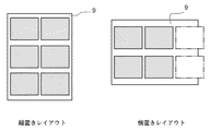
効率を劣化させずに、多種多様のサイズのパネルを生産できるラインを構築するため、最近では、図4に示すようにガラス基板9の向きを90度回転させて露光し、パネルレイアウトのバリエーションを増やす方法がとられている。
【0004】
しかし、従来の露光装置では、ガラス基板の向きを90度回転させる手段が無く、どうしても90度回転させるためには、露光装置内部にあってガラス基板を保持する保持板(以下プレートチャックという)の取付け方向を変更し、90度回転の要望に対応していた。
【0005】
さらに露光装置の内部の保持板の変更以外にも、露光の前工程の機械から露光装置にガラス基板を搬送する際に、ガラス基板を90度回転させることが必要であり、ガラス基板搬送機構にも改造が必要であった。
【0006】
【発明が解決しようとする課題】
このように、ガラス基板を90度回転させるメリットはあっても、実際には製造ラインの改造負荷が多大であり、仮に改造を行ったとしても、以下のような欠点があった。
▲1▼ ガラス基板を保持するプレートチャックは2種類必要である。
▲2▼ 2種類のプレートチャックをパネルレイアウトの変更ごとに露光装置に搭載し直さなければならない。
▲3▼ 露光装置にガラス基板を搬入する際に、ガラス基板を90度回転させる機構が必要である。
【0007】
また、2通りの保持方法が可能なチャックを作る方法もあるが、チャックが大きくなり、重くなることから、露光装置のステージ精度劣化につながる。それでも、上記項目中の▲3▼は不可欠である。
【0008】
本発明の目的は、1種類のチャックのみを用いて、露光方向に対し0から90度回転できるステージを用意し、2通りのガラス基板の位置決めが可能な露光装置を提供することである。
【0009】
【課題を解決するための手段】
上記課題を解決するための本発明に係る露光装置は、基板を露光する露光装置であって、X方向およびY方向に移動するステージと、前記基板を保持するチャックと、前記ステージに固定され、前記ステージの前記X方向の位置を計測する際に用いられるXバーミラーおよび前記ステージの前記Y方向の位置を計測する際に用いられるYバーミラーが取付けられた板と、前記板上に設けられ、前記チャックを支持して、前記板に対して前記チャックをXY面内で少なくとも90度回転させる回転機構と、を備え、前記回転機構は、前記基板の向きが前記基板のサイズと前記基板に露光されるパネルのサイズとに応じて求められた方向に合うように、前記チャックを回転させることを特徴とする。
【0011】
【実施例】
(第1の実施例)
本発明の第1の実施例について図面を参照しながら詳細に説明する。
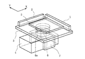
図1および図2は、本発明の第1の実施例に係わる露光装置に搭載するプレートステージの概念を示す斜視図である。
この露光装置に搭載される図1に示すプレートステージにおいて、1はX方向に面して配置されたXバーミラー、2はY方向に面して配置されたYバーミラー、3はXバーミラー1とYバーミラー2を固定しているバーミラー取付け板、4は露光用ステージを拘束しX方向に案内するX方向ガイド、5はガラス基板を固定する保持板としてのプレートチャック、6はプレートチャック5を回転させる回転機構、7はバーミラー取付け板3を搭載するX方向スライダである。
【0012】
バーミラー取付け板3は、被露光体であるガラス基板を位置合わせした後、露光できる露光用ステージを構成している。回転機構6は、X方向スライダ7の上に設置されており、バーミラー取付け板3の上に突出した回転可能な円盤6aを備え、該円盤6aでプレートチャック5を少なくとも90度回転可能に支持している。
【0013】
上記構成において、図示しないガラス基板がプレートチャック5に搬送されると、位置合わせを行った後、図中のY方向にスキャンし、露光される。必要に応じてスライダ7が図中X方向のスライド(ステップ)し、再度Y方向にスキャンしガラス基板を露光する。このような動作を繰り返し、ガラス基板全面を露光し終わると、ガラス基板はプレートチャック5から搬出され、次のガラス基板が再度プレートチャック5に搬送される。
【0014】
次に、同一サイズのガラス基板を用いて、生産するパネルのレイアウトを変更する場合は、図1に示す状態でプレートチャック5にガラス基板を保持した後、図2に示すように、プレートチャック回転機構6で該プレートチャック5を90度回転させることにより、露光方向に対するガラス基板の方向が90度変わり、同一サイズのガラス基板でありながら、別のパネルレイアウトが構築でき、別のサイズの液晶パネルを生産することができる。
【0015】
(第2の実施例)
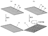
図3は本発明の第2の実施例の説明用斜視図である。
ガラス基板に縦横のストライプを描画するような製造工程においては、はじめに、図3(a)に示すように縦線8aを有するマスク8を用いて縦線を描画した後、図3(b)に示すようにガラス基板9を90度回転させ、同一マスク8を用いて露光することにより、横線を描画することができる。
この本発明の第2の実施例によれば、縦横ストライプ工程の場合、縦のストライプ用マスク1枚のみで、ガラス基板9上に縦横のストライプを描画することができる。
(第3の実施例)
次に、本発明の第3の実施例を構成する回転機構6は、ガラス基板9上に露光されるパネルのレイアウトを定義するジョブの入力に応じて求められた方向にガラス基板9が合うように、プレートチャック5を回転させる。
この本発明の第3の実施例によれば、ガラス基板9のサイズと希望するパネルサイズを入力することにより、露光装置が最適なガラス基板9の方向を計算し、自動的に回転機構6が0あるいは90度方向にガラス基板9の向きを変え、効率よくパネルを生産することができる。
【0016】
【デバイス生産方法の実施例】
次に上記説明した投影露光装置を利用したデバイスの生産方法の実施例を説明する。
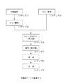
図5は微小デバイス(ICやLSI等の半導体チップ、液晶パネル、CCD、薄膜磁気ヘッド、マイクロマシン等)の製造のフローを示す。ステップ1(回路設計)ではデバイスのパターン設計を行う。ステップ2(マスク製作)では設計したパターンを形成したマスクを製作する。一方、ステップ3(ウエハ製造)ではシリコンやガラス等の材料を用いてウエハ(特に、ガラス基板)を製造する。ステップ4(ウエハプロセス)は前工程と呼ばれ、上記用意したマスクとウエハを用いて、リソグラフィ技術によってウエハ上に実際の回路を形成する。次のステップ5(組み立て)は後工程と呼ばれ、ステップ4によって作製されたウエハを用いて半導体チップ化する工程であり、アッセンブリ工程(ダイシング、ボンディング)、パッケージング工程(チップ封入)等の工程を含む。ステップ6(検査)ではステップ5で作製された半導体デバイスの動作確認テスト、耐久性テスト等の検査を行う。こうした工程を経て半導体デバイスが完成し、これが出荷(ステップ7)される。
【0017】
図6は上記ウエハプロセスの詳細なフローを示す。ステップ11(酸化)ではウエハの表面を酸化させる。ステップ12(CVD)ではウエハ表面に絶縁膜を形成する。ステップ13(電極形成)ではウエハ上に電極を蒸着によって形成する。ステップ14(イオン打込み)ではウエハにイオンを打ち込む。ステップ15(レジスト処理)ではウエハに感光剤を塗布する。ステップ16(露光)では上記説明した投影露光装置によってマスクの回路パターンをウエハに焼付露光する。ステップ17(現像)では露光したウエハを現像する。ステップ18(エッチング)では現像したレジスト像以外の部分を削り取る。ステップ19(レジスト剥離)ではエッチングが済んで不要となったレジストを取り除く。これらのステップを繰り返し行うことによって、ウエハ上に多重に回路パターンが形成される。
【0018】
本実施例の生産方法を用いれば、従来は製造が難しかった高集積度のデバイスを低コストに製造することができる。
【0019】
【発明の効果】
以上説明したように、本発明によれば、液晶パネル製造露光装置において、プレートチャックの交換や、プレートの搬送機構を変更すること無く、1枚のガラス基板を縦と横の2通りの方向に搭載可能になり、その結果、1枚のガラス基板から生産できるパネルレイアウトのバリエーションが増加する。
【図面の簡単な説明】
【図1】 本発明の第1の実施例に係わる露光装置に搭載するプレートステージの概念を示す斜視図である。
【図2】 図1におけるチャックを90度回転させた状態を表した斜視図である。
【図3】 本発明の実施例に係わるガラス基板を90度回転させ、縦横ストライプを描画する方法を表した斜視図である。
【図4】 従来のパネルレイアウトを表した図である。
【図5】 微小デバイスの製造の流れを示す図である。
【図6】 図5におけるウエハプロセスの詳細な流れを示す図である。
【符号の説明】
1:Xバーミラー、2:Yバーミラー、3:バーミラー取付け板(露光用ステージを構成する)、4:X方向ガイド、5:プレートチャック(保持板)、6:回転機構、7:X方向スライダ、8:マスク(原版)、9:ガラス基板(被露光体)。[0001]
BACKGROUND OF THE INVENTION
The present invention relates to an exposure apparatus for transferring a pattern such as a mask as an original to a substrate as an exposure object in an exposure apparatus used for manufacturing a liquid crystal panel.
[0002]
[Prior art]
In recent years, the application fields of liquid crystal panels have been diversified, and as a result, panel manufacturers have been forced to respond to the demand for a large number of panel sizes.
The size of the glass substrate used in a normal liquid crystal panel production line is one type, and if the panel size to be manufactured is determined, the layout of the liquid crystal panel that can be manufactured from one glass substrate is naturally determined to be several types. Setting an unreasonable panel layout can reduce efficiency.
[0003]
In order to build a line that can produce panels of various sizes without degrading efficiency, recently, as shown in FIG. 4, the
[0004]
However, in the conventional exposure apparatus, there is no means for rotating the direction of the glass substrate by 90 degrees. To rotate the glass substrate by 90 degrees, a holding plate (hereinafter referred to as a plate chuck) that holds the glass substrate inside the exposure apparatus is unavoidable. The mounting direction was changed to meet the demand for 90 ° rotation.
[0005]
Furthermore, in addition to changing the holding plate inside the exposure apparatus, it is necessary to rotate the glass substrate by 90 degrees when transferring the glass substrate from the machine before the exposure to the exposure apparatus. Even remodeling was necessary.
[0006]
[Problems to be solved by the invention]
As described above, even if there is a merit of rotating the glass substrate by 90 degrees, there is actually a great remodeling load on the production line, and even if remodeling is performed, there are the following drawbacks.
(1) Two types of plate chucks for holding the glass substrate are required.
(2) Two types of plate chucks must be remounted on the exposure apparatus every time the panel layout is changed.
(3) A mechanism for rotating the glass substrate by 90 degrees is necessary when the glass substrate is carried into the exposure apparatus.
[0007]
There is also a method of making a chuck that can be held in two ways, but the chuck becomes larger and heavier, leading to deterioration in stage accuracy of the exposure apparatus. Nevertheless, (3) in the above item is indispensable.
[0008]
An object of the present invention is to provide an exposure apparatus capable of positioning two kinds of glass substrates by preparing a stage that can rotate from 0 to 90 degrees with respect to the exposure direction using only one type of chuck .
[0009]
[Means for Solving the Problems]
An exposure apparatus according to the present invention for solving the above problems is an exposure apparatus that exposes a substrate, a stage that moves in the X direction and the Y direction, a chuck that holds the substrate, and is fixed to the stage. An X bar mirror used when measuring the position of the stage in the X direction and a plate to which a Y bar mirror used when measuring the position of the stage in the Y direction is attached; and provided on the plate; A rotation mechanism that supports the chuck and rotates the chuck at least 90 degrees in the XY plane with respect to the plate, the rotation mechanism exposing the substrate size and the substrate. The chuck is rotated so as to match the direction determined according to the size of the panel to be adjusted .
[0011]
【Example】
(First embodiment)
A first embodiment of the present invention will be described in detail with reference to the drawings.
1 and 2 are perspective views showing the concept of a plate stage mounted on an exposure apparatus according to the first embodiment of the present invention.
In the plate stage shown in FIG. 1 mounted in this exposure apparatus, 1 is an X bar mirror arranged facing the X direction, 2 is a Y bar mirror arranged facing the Y direction, and 3 is an
[0012]
The bar
[0013]
In the above configuration, when a glass substrate (not shown) is conveyed to the
[0014]
Next, when changing the layout of the panel to be produced using the same size glass substrate, the glass substrate is held on the
[0015]
(Second embodiment)
FIG. 3 is a perspective view for explaining a second embodiment of the present invention.
In a manufacturing process in which vertical and horizontal stripes are drawn on a glass substrate, first, vertical lines are drawn using a
According to the second embodiment of the present invention, in the vertical and horizontal stripe process, vertical and horizontal stripes can be drawn on the
(Third embodiment)
Next, the
According to the third embodiment of the present invention, by inputting the size of the
[0016]
[Example of device production method]
Next, an embodiment of a device production method using the above-described projection exposure apparatus will be described.
FIG. 5 shows a manufacturing flow of a microdevice (a semiconductor chip such as an IC or LSI, a liquid crystal panel, a CCD, a thin film magnetic head, a micromachine, etc.). In step 1 (circuit design), a device pattern is designed. In step 2 (mask production), a mask on which the designed pattern is formed is produced. On the other hand, in step 3 (wafer manufacture), a wafer (particularly a glass substrate) is manufactured using a material such as silicon or glass. Step 4 (wafer process) is called a pre-process, and an actual circuit is formed on the wafer by lithography using the prepared mask and wafer. The next step 5 (assembly) is referred to as a post-process, and is a process for forming a semiconductor chip using the wafer produced in
[0017]
FIG. 6 shows a detailed flow of the wafer process. In step 11 (oxidation), the wafer surface is oxidized. In step 12 (CVD), an insulating film is formed on the wafer surface. In step 13 (electrode formation), an electrode is formed on the wafer by vapor deposition. In step 14 (ion implantation), ions are implanted into the wafer. In step 15 (resist process), a photosensitive agent is applied to the wafer. In step 16 (exposure), the circuit pattern of the mask is printed on the wafer by exposure using the projection exposure apparatus described above. In step 17 (development), the exposed wafer is developed. In step 18 (etching), portions other than the developed resist image are removed. In step 19 (resist stripping), unnecessary resist after etching is removed. By repeatedly performing these steps, multiple circuit patterns are formed on the wafer.
[0018]
By using the production method of this embodiment, a highly integrated device that has been difficult to manufacture can be manufactured at low cost.
[0019]
【The invention's effect】
As described above, according to the present invention, in a liquid crystal panel manufacturing exposure apparatus, a single glass substrate can be placed in two directions, vertical and horizontal, without changing the plate chuck or changing the plate transport mechanism. As a result, the variation of panel layouts that can be produced from a single glass substrate is increased.
[Brief description of the drawings]
FIG. 1 is a perspective view showing a concept of a plate stage mounted on an exposure apparatus according to a first embodiment of the present invention.
2 is a perspective view showing a state in which the chuck in FIG. 1 is rotated by 90 degrees. FIG.
FIG. 3 is a perspective view illustrating a method of drawing vertical and horizontal stripes by rotating a glass substrate according to an embodiment of the present invention by 90 degrees.
FIG. 4 is a diagram showing a conventional panel layout.
FIG. 5 is a diagram showing a flow of manufacturing a microdevice.
6 is a diagram showing a detailed flow of the wafer process in FIG. 5. FIG.
[Explanation of symbols]
1: X bar mirror, 2: Y bar mirror, 3: Bar mirror mounting plate (constituting exposure stage), 4: X direction guide, 5: Plate chuck (holding plate ), 6: Rotating mechanism, 7: X direction slider, 8: Mask (original), 9: Glass substrate (exposed body).
Claims (6)
X方向およびY方向に移動するステージと、
前記基板を保持するチャックと、
前記ステージに固定され、前記ステージの前記X方向の位置を計測する際に用いられるXバーミラーおよび前記ステージの前記Y方向の位置を計測する際に用いられるYバーミラーが取付けられた板と、
前記板上に設けられ、前記チャックを支持して、前記板に対して前記チャックをXY面内で少なくとも90度回転させる回転機構と、を備え、
前記回転機構は、前記基板の向きが前記基板のサイズと前記基板に露光されるパネルのサイズとに応じて求められた方向に合うように、前記チャックを回転させることを特徴とする露光装置。An exposure apparatus for exposing a substrate,
A stage that moves in the X and Y directions;
A chuck for holding the substrate;
An X-bar mirror fixed to the stage and used for measuring the position of the stage in the X direction, and a plate to which a Y-bar mirror used for measuring the position of the stage in the Y direction is attached;
A rotation mechanism provided on the plate, supporting the chuck, and rotating the chuck at least 90 degrees in the XY plane with respect to the plate ;
The exposure apparatus characterized in that the rotating mechanism rotates the chuck so that the orientation of the substrate matches a direction determined according to a size of the substrate and a size of a panel exposed to the substrate .
露光された前記基板を現像するステップと、を備えることを特徴とするデバイス製造方法。Using an exposure apparatus according to any one of claims 1 to 5, comprising the steps of exposing a substrate,
And developing the exposed substrate. A device manufacturing method comprising:
Priority Applications (1)
| Application Number | Priority Date | Filing Date | Title |
|---|---|---|---|
| JP2000060269A JP4428792B2 (en) | 2000-03-06 | 2000-03-06 | Exposure equipment |
Applications Claiming Priority (1)
| Application Number | Priority Date | Filing Date | Title |
|---|---|---|---|
| JP2000060269A JP4428792B2 (en) | 2000-03-06 | 2000-03-06 | Exposure equipment |
Publications (3)
| Publication Number | Publication Date |
|---|---|
| JP2001249462A JP2001249462A (en) | 2001-09-14 |
| JP2001249462A5 JP2001249462A5 (en) | 2007-04-05 |
| JP4428792B2 true JP4428792B2 (en) | 2010-03-10 |
Family
ID=18580611
Family Applications (1)
| Application Number | Title | Priority Date | Filing Date |
|---|---|---|---|
| JP2000060269A Expired - Fee Related JP4428792B2 (en) | 2000-03-06 | 2000-03-06 | Exposure equipment |
Country Status (1)
| Country | Link |
|---|---|
| JP (1) | JP4428792B2 (en) |
Families Citing this family (4)
| Publication number | Priority date | Publication date | Assignee | Title |
|---|---|---|---|---|
| JP4594745B2 (en) * | 2005-01-14 | 2010-12-08 | パナソニック株式会社 | Method for manufacturing member having antireflection structure |
| WO2008065977A1 (en) * | 2006-11-27 | 2008-06-05 | Nikon Corporation | Exposure method, pattern forming method, exposure device, and device manufacturing method |
| JP5549233B2 (en) * | 2010-01-18 | 2014-07-16 | 凸版印刷株式会社 | Color filter substrate exposure method |
| JP5542456B2 (en) * | 2010-01-18 | 2014-07-09 | 凸版印刷株式会社 | Color filter substrate exposure method |
-
2000
- 2000-03-06 JP JP2000060269A patent/JP4428792B2/en not_active Expired - Fee Related
Also Published As
| Publication number | Publication date |
|---|---|
| JP2001249462A (en) | 2001-09-14 |
Similar Documents
| Publication | Publication Date | Title |
|---|---|---|
| US8193100B2 (en) | Exposure mask manufacturing method, drawing apparatus, semiconductor device manufacturing method, and mask blanks product | |
| JP4794882B2 (en) | Scanning exposure apparatus and scanning exposure method | |
| US7289194B2 (en) | Positioning apparatus, exposure apparatus, and device manufacturing method | |
| JP2008103703A (en) | Substrate holding apparatus, exposure apparatus including the substrate holding apparatus, and device manufacturing method | |
| JP2001332480A (en) | Original chuck, exposure apparatus having the original chuck, and method of manufacturing semiconductor device | |
| JPH10321515A (en) | Semiconductor exposure equipment | |
| JP4332409B2 (en) | Substrate holding mechanism, exposure apparatus using the same, and device manufacturing method | |
| JP4428792B2 (en) | Exposure equipment | |
| JP2001127144A (en) | Substrate suction holding method, substrate suction holding apparatus, exposure apparatus and device manufacturing method using the substrate suction holding apparatus | |
| JP2006310446A (en) | Semiconductor device manufacturing method and exposure apparatus | |
| JP3634539B2 (en) | Mask holding apparatus, exposure apparatus, device manufacturing method, and mask structure | |
| US6309212B1 (en) | Substrate conveying system and device manufacturing method using the same | |
| JP2000228355A (en) | Semiconductor exposure apparatus and device manufacturing method | |
| JP3658091B2 (en) | Scanning exposure method and device manufacturing method using the method | |
| JP2000182936A (en) | Exposure apparatus and device manufacturing method | |
| JPH1174190A (en) | X-ray exposure equipment | |
| JP3548375B2 (en) | Coating method and apparatus | |
| JP2000138161A (en) | Exposure equipment | |
| JPH10308434A (en) | Positioning apparatus, mirror bending detecting method, positioning method and device manufacturing method | |
| JP3473821B2 (en) | Exposure amount setting method, exposure method, exposure apparatus, and device manufacturing method | |
| JP3483403B2 (en) | Exposure equipment | |
| JP2023173758A (en) | Exposure device, exposure method, and article manufacturing method | |
| US6856404B2 (en) | Scanning exposure method and apparatus, and device manufacturing method using the same | |
| KR20040016067A (en) | Method for exposing photo resist film and exposure equipment using the same | |
| JP2003297723A (en) | Alignment method, exposure method and semiconductor device manufacturing method |
Legal Events
| Date | Code | Title | Description |
|---|---|---|---|
| A521 | Written amendment |
Free format text: JAPANESE INTERMEDIATE CODE: A523 Effective date: 20070216 |
|
| A621 | Written request for application examination |
Free format text: JAPANESE INTERMEDIATE CODE: A621 Effective date: 20070216 |
|
| RD01 | Notification of change of attorney |
Free format text: JAPANESE INTERMEDIATE CODE: A7421 Effective date: 20090406 |
|
| A131 | Notification of reasons for refusal |
Free format text: JAPANESE INTERMEDIATE CODE: A131 Effective date: 20090630 |
|
| A521 | Written amendment |
Free format text: JAPANESE INTERMEDIATE CODE: A523 Effective date: 20090728 |
|
| TRDD | Decision of grant or rejection written | ||
| A01 | Written decision to grant a patent or to grant a registration (utility model) |
Free format text: JAPANESE INTERMEDIATE CODE: A01 Effective date: 20091208 |
|
| A01 | Written decision to grant a patent or to grant a registration (utility model) |
Free format text: JAPANESE INTERMEDIATE CODE: A01 |
|
| A61 | First payment of annual fees (during grant procedure) |
Free format text: JAPANESE INTERMEDIATE CODE: A61 Effective date: 20091215 |
|
| FPAY | Renewal fee payment (event date is renewal date of database) |
Free format text: PAYMENT UNTIL: 20121225 Year of fee payment: 3 |
|
| R150 | Certificate of patent or registration of utility model |
Free format text: JAPANESE INTERMEDIATE CODE: R150 |
|
| A521 | Written amendment |
Free format text: JAPANESE INTERMEDIATE CODE: A523 Effective date: 20070216 |
|
| FPAY | Renewal fee payment (event date is renewal date of database) |
Free format text: PAYMENT UNTIL: 20131225 Year of fee payment: 4 |
|
| LAPS | Cancellation because of no payment of annual fees |