JP4332409B2 - Substrate holding mechanism, exposure apparatus using the same, and device manufacturing method - Google Patents
Substrate holding mechanism, exposure apparatus using the same, and device manufacturing method Download PDFInfo
- Publication number
- JP4332409B2 JP4332409B2 JP2003372036A JP2003372036A JP4332409B2 JP 4332409 B2 JP4332409 B2 JP 4332409B2 JP 2003372036 A JP2003372036 A JP 2003372036A JP 2003372036 A JP2003372036 A JP 2003372036A JP 4332409 B2 JP4332409 B2 JP 4332409B2
- Authority
- JP
- Japan
- Prior art keywords
- substrate
- holding
- stage
- holding mechanism
- holding portion
- Prior art date
- Legal status (The legal status is an assumption and is not a legal conclusion. Google has not performed a legal analysis and makes no representation as to the accuracy of the status listed.)
- Expired - Fee Related
Links
- 239000000758 substrate Substances 0.000 title claims description 260
- 230000007246 mechanism Effects 0.000 title claims description 95
- 238000004519 manufacturing process Methods 0.000 title claims description 10
- 238000001179 sorption measurement Methods 0.000 claims description 4
- 230000014759 maintenance of location Effects 0.000 claims 1
- 238000012546 transfer Methods 0.000 description 18
- 238000012937 correction Methods 0.000 description 9
- 238000000034 method Methods 0.000 description 9
- 239000004065 semiconductor Substances 0.000 description 9
- 230000032258 transport Effects 0.000 description 8
- 230000007723 transport mechanism Effects 0.000 description 7
- 230000000694 effects Effects 0.000 description 3
- 239000011521 glass Substances 0.000 description 3
- 238000006073 displacement reaction Methods 0.000 description 2
- 238000005530 etching Methods 0.000 description 2
- 230000005484 gravity Effects 0.000 description 2
- 238000007689 inspection Methods 0.000 description 2
- 238000012360 testing method Methods 0.000 description 2
- 230000015572 biosynthetic process Effects 0.000 description 1
- 239000003795 chemical substances by application Substances 0.000 description 1
- 238000012790 confirmation Methods 0.000 description 1
- 238000013461 design Methods 0.000 description 1
- 238000011161 development Methods 0.000 description 1
- 230000008034 disappearance Effects 0.000 description 1
- 238000005538 encapsulation Methods 0.000 description 1
- 239000010408 film Substances 0.000 description 1
- 238000005468 ion implantation Methods 0.000 description 1
- 150000002500 ions Chemical class 0.000 description 1
- 239000004973 liquid crystal related substance Substances 0.000 description 1
- 238000001459 lithography Methods 0.000 description 1
- 238000012423 maintenance Methods 0.000 description 1
- 230000008531 maintenance mechanism Effects 0.000 description 1
- 239000000463 material Substances 0.000 description 1
- 238000005259 measurement Methods 0.000 description 1
- 230000003647 oxidation Effects 0.000 description 1
- 238000007254 oxidation reaction Methods 0.000 description 1
- 238000012858 packaging process Methods 0.000 description 1
- 238000002360 preparation method Methods 0.000 description 1
- 230000002265 prevention Effects 0.000 description 1
- 238000012545 processing Methods 0.000 description 1
- 230000001105 regulatory effect Effects 0.000 description 1
- 229910052710 silicon Inorganic materials 0.000 description 1
- 239000010703 silicon Substances 0.000 description 1
- 239000010409 thin film Substances 0.000 description 1
- 238000007740 vapor deposition Methods 0.000 description 1
Images


Classifications
-
- G—PHYSICS
- G03—PHOTOGRAPHY; CINEMATOGRAPHY; ANALOGOUS TECHNIQUES USING WAVES OTHER THAN OPTICAL WAVES; ELECTROGRAPHY; HOLOGRAPHY
- G03F—PHOTOMECHANICAL PRODUCTION OF TEXTURED OR PATTERNED SURFACES, e.g. FOR PRINTING, FOR PROCESSING OF SEMICONDUCTOR DEVICES; MATERIALS THEREFOR; ORIGINALS THEREFOR; APPARATUS SPECIALLY ADAPTED THEREFOR
- G03F7/00—Photomechanical, e.g. photolithographic, production of textured or patterned surfaces, e.g. printing surfaces; Materials therefor, e.g. comprising photoresists; Apparatus specially adapted therefor
- G03F7/70—Microphotolithographic exposure; Apparatus therefor
- G03F7/70691—Handling of masks or workpieces
- G03F7/707—Chucks, e.g. chucking or un-chucking operations or structural details
- G03F7/70708—Chucks, e.g. chucking or un-chucking operations or structural details being electrostatic; Electrostatically deformable vacuum chucks
Description
本発明は、半導体露光装置などにおいて用いられる、マスクやレチクル、または半導体ウエハやガラス基板などの薄板状の基板を保持する基板保持機構に関する。 The present invention relates to a substrate holding mechanism for holding a thin plate-like substrate such as a mask, a reticle, or a semiconductor wafer or a glass substrate used in a semiconductor exposure apparatus or the like.
従来、半導体露光装置においてレチクルやウエハを保持する基板保持機構は、基板の下面または上面あるいは表面または裏面など、一面を保持していた。すなわち、特許文献1〜3に示されるように、露光用のステージは、主として、基板の下面を保持し、ステージへ基板を搬入搬出する基板搬送機構においては、基板の下面または、上面のいずれか一方を保持していた。また、特許文献4に示されるように基板を縦向き(垂直)に保持する場合もあるが、この場合も、ステージおよび基板搬送機構は、それぞれ一面を保持していた。特許文献4においては、露光用のステージも、該ステージへ基板を搬入搬出する基板搬送機構も基板の裏面を保持する。
Conventionally, a substrate holding mechanism for holding a reticle or wafer in a semiconductor exposure apparatus holds one surface such as a lower surface or an upper surface, a front surface or a back surface of the substrate. That is, as disclosed in Patent Documents 1 to 3, the exposure stage mainly holds the lower surface of the substrate, and in the substrate transport mechanism that carries the substrate in and out of the stage, either the lower surface or the upper surface of the substrate. Was holding one. Also, as shown in
ここで、搬送機構における基板保持部と、ステージの基板保持部が、特許文献1および4に記載されているように基板の同一面上を保持する場合を考えると、搬送機構とステージの各基板保持機構の基板保持部は、互いに干渉を避けるために、それぞれ、保持面積が制約されてしまう。その結果、近年の搬送速度の高速化に伴う保持力増加の要求に応えることが困難となってきている。また、搬送機構とステージ間に発生するチルト補正が困難であり、補正するためには、アクチュエータによる補正機構を設ける必要がある。
Here, considering the case where the substrate holding unit in the transfer mechanism and the substrate holding unit of the stage hold the same surface of the substrate as described in
これに対して、特許文献2に記載されているように搬送機構における基板保持部とステージの基板保持部が、基板の異なる面を保持する場合を考えると、搬送機構およびステージの基板保持部は、保持面積について互いの制約を受けることは無い。また、両者間に発生するチルトの補正も、アクチュエータを構成することなく容易に補正可能である。但し、その場合は、板バネ構造等、ひずみを許容できる構造で構成される必要があり、その結果、単独で基板を保持している時には、その弾性のため、基板の面精度を維持するのは困難である。
特許文献4には、基板の同一面上を保持する場合についてではあるが、チルト補正機構を用いた例が記載されている。
On the other hand, considering the case where the substrate holding unit in the transfer mechanism and the substrate holding unit of the stage hold different surfaces of the substrate as described in Patent Document 2, the transfer mechanism and the substrate holding unit of the stage are The holding area is not restricted by each other. In addition, the tilt generated between the two can be easily corrected without configuring an actuator. However, in that case, it is necessary to be configured with a structure that can tolerate strain, such as a leaf spring structure. As a result, when the substrate is held alone, the surface accuracy of the substrate is maintained due to its elasticity. It is difficult.
また、基板を上面から吸着保持する場合、基板保持部の吸着力が消失すると、基板が落下して破損する恐れがある。特許文献3にはこのような吸着力の消失に基づく基板の落下を防止する手段が開示されている。
本発明は、基板保持機構における保持力および保持精度の向上を図ることを課題とする。 An object of the present invention is to improve the holding force and holding accuracy in a substrate holding mechanism.
上記の課題を解決するため本発明の基板保持機構は、基板の一方の面を吸着する第1保持部と、前記基板の他方の面に当接して前記基板を吸着する第2保持部と、前記第2保持部を移動させる機構と、前記第1保持部を第2保持部側へ付勢するバネとを有し、前記バネは、前記基板が前記第1保持部に押付けられた状態で前記第2保持部を前記基板に対向させた際に、前記第2保持部と前記基板との間に空間が形成されるように収縮可能であることを特徴とする。 Substrate holding mechanism of the present invention for solving the aforementioned problem, a second holding unit for attracting the first holding part for adsorbing one surface of the substrate, the contact with the substrate on the other surface of the substrate, a mechanism for moving the second holding unit, wherein the first holding portion have a spring for biasing the second holding portion, said spring, in a state where the substrate is pressed against the first holding portion When the second holding portion is opposed to the substrate, the second holding portion can contract so that a space is formed between the second holding portion and the substrate .
本発明によれば、基板の一方の面に吸着する第1保持部と、前記基板の他方の面に当接する第2保持部とにより、基板の両面を同時に保持する。
このため、基板に同時に接触可能な面を増やし、基板の保持力を増加することができ、かつ保持精度を向上させることができる。
その結果、本発明の基板保持機構を適用した露光装置や半導体製造装置などの装置においては、装置全体の基板搬送スループット向上および搬送精度の向上を実現することができる。
According to the present invention, both surfaces of the substrate are simultaneously held by the first holding portion that is attracted to one surface of the substrate and the second holding portion that is in contact with the other surface of the substrate.
For this reason, the surface which can be simultaneously contacted with a board | substrate can be increased, the holding power of a board | substrate can be increased, and a holding | maintenance precision can be improved.
As a result, in an apparatus such as an exposure apparatus or a semiconductor manufacturing apparatus to which the substrate holding mechanism of the present invention is applied, it is possible to improve the substrate transfer throughput and the transfer accuracy of the entire apparatus.
以下、本発明の実施態様を列挙する。
[実施態様1]
基板の両面の一方を吸着する第1保持部と、他方に当接してそれを支持する第2保持部と、基板を吸着した第1保持部を第2保持部側へ付勢する付勢手段とを有することを特徴とする基板保持機構。
この基板保持機構において、基板は一方の面を第1保持部により吸着され、付勢手段により第2保持部側へ付勢される。その結果、基板は第1保持部と第2保持部とに挟み込まれ、より大きな保持力で保持される。また、基板は、前記他方の面を第2保持部に押し付けられてその面位置を第2保持部により規制されるため、高い位置精度で保持される。さらに、第2保持部の基板との当接面の面精度ならびに第1および第2保持部による基板支持位置を適切に設定することにより、保持された基板の面精度が維持または修正され、搬送中の基板の位置計測が可能となり、位置計測用の他の支持機構がなくとも、基板の位置ずれ量の計測、面精度の計測等が可能となる。
なお、特許文献3の落下防止手段は、吸着力消失時に吸着から解放された基板を受け止めるもので、通常は基板から離れている。したがって、保持力を向上させる作用はない。また、基板の面位置を位置決めしたり、面精度を維持または修正する作用もない。
付勢手段は、例えば板バネであり、他の基板保持機構との間で基板を受け渡しする際には第1保持部の基板保持面を受け渡し相手の基板保持面に平行に倣わせるチルト補正機構として作用する。そのため、他の基板保持機構が基板を保持した状態で、同時に第1保持部が基板を保持することができ、基板受け渡し時における基板の位置ずれの発生を抑えることができる。
The embodiments of the present invention are listed below.
[Embodiment 1]
A first holding part that sucks one of both surfaces of the substrate, a second holding part that contacts and supports the other, and a biasing means that biases the first holding part that sucks the substrate toward the second holding part And a substrate holding mechanism.
In this substrate holding mechanism, one surface of the substrate is adsorbed by the first holding portion and is urged toward the second holding portion by the urging means. As a result, the substrate is sandwiched between the first holding unit and the second holding unit and held with a larger holding force. Further, the substrate is held with high positional accuracy because the other surface is pressed against the second holding portion and the surface position thereof is regulated by the second holding portion. Further, by appropriately setting the surface accuracy of the contact surface of the second holding unit with the substrate and the substrate support position by the first and second holding units, the surface accuracy of the held substrate is maintained or corrected and transported. The position of the inside substrate can be measured, and even if there is no other support mechanism for position measurement, it is possible to measure the amount of positional deviation of the substrate, measure the surface accuracy, and the like.
Note that the fall prevention means of
The biasing means is, for example, a leaf spring, and when the substrate is transferred to or from another substrate holding mechanism, the tilt correction is performed so that the substrate holding surface of the first holding unit is transferred in parallel with the counterpart substrate holding surface. Acts as a mechanism. Therefore, the first holding unit can hold the substrate at the same time while the other substrate holding mechanism holds the substrate, and the occurrence of the displacement of the substrate at the time of transferring the substrate can be suppressed.
[実施態様2]
前記第2保持部を、基板保持位置と保持解除位置とに駆動する手段をさらに有することを特徴とする実施態様1に記載の基板保持機構。
このような駆動手段を有することにより、他の基板保持機構との間で基板を受け渡しする際には、第2保持部を、受け渡しすべき基板の移動経路から保持解除位置に退避させて、該基板との干渉を避けることができる。
[実施態様3]
前記第1保持部が基板の上面を吸着し、前記第2保持部が該基板の下面を支持することにより、該前記基板を下向きに保持することを特徴とする実施態様1または2に記載の基板保持機構。
本発明の基板保持機構は、特に、基板を下向きに保持する基板保持手段として好適なものである。
[Embodiment 2]
2. The substrate holding mechanism according to claim 1, further comprising means for driving the second holding unit to a substrate holding position and a holding release position.
By having such a driving means, when transferring the substrate to or from another substrate holding mechanism, the second holding portion is retracted from the movement path of the substrate to be transferred to the holding release position, Interference with the substrate can be avoided.
[Embodiment 3]
3. The embodiment according to claim 1, wherein the first holding unit sucks an upper surface of the substrate and the second holding unit supports the lower surface of the substrate to hold the substrate downward. Substrate holding mechanism.
The substrate holding mechanism of the present invention is particularly suitable as a substrate holding means for holding the substrate downward.
[実施態様4]
実施態様1〜3のいずれか1つに記載の基板保持機構を有することを特徴とする露光装置。
本発明の基板保持機構は、露光装置において、露光原版としてのレチクルやマスク、あるいは被露光基板としての半導体ウエハやガラス基板を搬送する搬送ロボットまたはこれらの基板を位置決めするステージ等で露光原版や被露光基板を保持するために用いることができる。
例えば、基板をレチクルとし、基板保持機構をレチクル搬送系に構成した場合、レチクルの両面を保持し、高速搬送するレチクル搬送系を構成し、前記搬送系の搬送中に基板位置を計測し、レチクルステージとの同時吸着によって、精度良くレチクルの受け渡しが可能な受け渡し機構を実現することができ、露光装置のスループット向上および搬送精度向上を果たすことができる。
[Embodiment 4]
An exposure apparatus comprising the substrate holding mechanism according to any one of Embodiments 1 to 3.
In the exposure apparatus, the substrate holding mechanism of the present invention is used in an exposure apparatus such as a reticle or mask as an exposure original plate, a transfer robot for transferring a semiconductor wafer or glass substrate as an exposure substrate, or a stage for positioning these substrates. It can be used to hold the exposed substrate.
For example, if the substrate is a reticle and the substrate holding mechanism is configured as a reticle transport system, a reticle transport system that holds both sides of the reticle and transports at high speed is configured, and the substrate position is measured during transport of the transport system, and the reticle By simultaneous suction with the stage, it is possible to realize a delivery mechanism capable of delivering the reticle with high accuracy, and it is possible to improve the throughput of the exposure apparatus and the conveyance accuracy.
以下、図面を用いて本発明の実施例を説明する。
[第1の実施例]
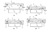
第1の実施例として、露光装置内の基板保持機構における、ステージと搬送機構間での基板の受け渡しについて、保持対象がレチクルである場合を例として説明する。
図1は本発明の一実施例に係る基板搬送装置における基板保持機構の構成を示す。同図の基板保持機構1は、基板搬送装置において、基板8を保持するもので、第1の基板保持部としての上面保持部2、3、第2の基板保持部としての下面保持部6、7を有する。上面保持部2、3は、真空吸着力または静電吸着力により、基板を吸着保持するものである。上面保持部2、3はこの上面保持部2、3を下面保持部6、7側へ付勢する付勢手段4、5を介して搬送ハンド等の搬送部20に取り付けられている。この付勢手段4、5は、例えば板バネである。付勢手段4、5は、上面保持部2、3を基板8へ押し付け、かつ基板8を下面保持部6、7に押し付けることにより、基板8を両面から同時に保持可能にしている。また、この付勢手段4、5は、他の基板保持機構であるステージ9との基板受け渡しの際に、ステージ9に搭載された基板の上面に対する上面保持部2、3のチルトを補正するチルト補正機構として作用し、ステージ9と上面保持部2、3との間で基板の同時保持を可能とする。
Embodiments of the present invention will be described below with reference to the drawings.
[First embodiment]
As a first embodiment, an explanation will be given of a case where a substrate to be held between a stage and a transfer mechanism in a substrate holding mechanism in an exposure apparatus is a reticle as an example.
FIG. 1 shows a configuration of a substrate holding mechanism in a substrate transfer apparatus according to an embodiment of the present invention. The substrate holding mechanism 1 shown in the figure holds the
下面保持部6、7は、例えば開閉式の機構を有し、他の基板保持機構との基板受け渡しの際には干渉防止のために基板端面より外側へ開く。一方、基板を搬送中には基板の下へ差し込まれるように閉じることにより、上面保持部2、3と同時に基板を保持し、基板の保持力をかせぐとともに、搬送中のトラブルにより、上面保持部2、3の保持力が低下した際の基板の落下防止に用いられる。
また、保持機構6、7が基板を保持する時の接触面の面精度が保証されるように構成することにより、搬送中の基板の面精度を保証することができる。この場合、搬送経路中、ステージ9に基板が受け渡されていない状態においても、レチクルのアライメントマークの計測、面精度の計測が可能となる。
The lower
Further, by configuring the holding
図1の基板保持機構とステージとの間の基板受け渡しのシーケンスについて説明する。
最初に、ステージ上の基板を基板保持機構が受け取る時のシーケンスついて、図2、3を用いて説明する。
受け渡しの初期状態として、ステージ9が基板8を水平または略水平に保持していることとする。また、ステージ9と基板保持機構1がZ方向(鉛直方向)に離れており、基板保持機構1は基板8を保持していないこととする。そして、基板保持機構1の下面保持部6、7は、基板8との干渉を防ぐために、基板保持機構1の端面において外側に開いているものとする(図3(a))。
基板保持機構1が基板を受け取るためには、まず、基板の上面保持部2、3が基板8の上面に接するように、基板保持機構1をZ方向に下降するか、または、ステージ9をZ方向に上昇させる(図2ステップ1)。
上面保持部2、3は、上方より基板8の上面に接したところで、基板8を保持する(図2ステップ2、図3(b))。このときステージ9と基板保持機構1の平行度が出ていない場合や、基板8の面精度が悪く、基板8の上面と基板保持機構1の平行度が出ていない場合においても、チルト補正機構として機能する付勢手段4、5により、上面保持部2、3は基板8の上面に倣うことができる。
また、この上面保持部2、3の基板保持の準備(例えば、静電チャックであれば電圧の印加、真空保持であれば、バキュームの吸引など)をZ方向への駆動と並列に処理することにより、受け渡し時間の短縮が可能となる。
A substrate transfer sequence between the substrate holding mechanism and the stage of FIG. 1 will be described.
First, the sequence when the substrate holding mechanism receives the substrate on the stage will be described with reference to FIGS.
As an initial state of delivery, it is assumed that the stage 9 holds the
In order for the substrate holding mechanism 1 to receive the substrate, first, the substrate holding mechanism 1 is lowered in the Z direction so that the upper
The upper
In addition, preparation for holding the substrate of the upper surface holding portions 2 and 3 (for example, application of voltage in the case of electrostatic chuck, suction of vacuum in the case of vacuum holding) is processed in parallel with driving in the Z direction. Thus, the delivery time can be shortened.
上面保持部2、3が基板8を保持したことが確認された後で、ステージ9は基板を解放する(図2ステップ31)。このようにして基板を受け渡す機構と受け取る機構が同時に基板を保持するタイミングを取ることにより、受け渡しの前後での基板の位置精度を上げることができる。
また、基板保持機構1の下面保持部6、7を閉じる。すなわち、下面保持部6、7を基板8の下面に移動する(図2ステップ32)。このとき、ステップ32をステップ31と並行処理することも可能である。
ステージ9の基板解放(ステップ31)および下面保持部6、7の移動(ステップ32)が終わると(図3(c))、基板保持機構1をZ方向に上昇するか、または、ステージ9をZ方向に下降させる(図2ステップ41)。これにより、基板8の下面は付勢手段4、5の付勢力により下面保持部6、7に接し、同時に基板8の下面と、ステージ9の上面がZ方向に引き離される。以上により、基板保持機構1は、ステージ9より基板8を受け取る。
After it is confirmed that the upper
Further, the lower
When the substrate release of the stage 9 (step 31) and the movement of the lower
なお、さらに基板の保持力を向上させるために、下面保持部6、7にも、静電チャック、真空吸着などの制御機構を設けている場合には、基板8がステージ9からZ方向に離れ、下面保持部6、7に接したところで、下面保持部6、7で基板8を吸着保持する。この処理は、ステップ41と並行処理することも可能である(図2ステップ42)。
以上で、ステージ9から基板保持部1への受け渡しは完了する(図3(d))。
In order to further improve the holding force of the substrate, if the lower
Thus, the delivery from the stage 9 to the substrate holding unit 1 is completed (FIG. 3D).
次に、基板保持機構1から、ステージ9が基板8を受け取る場合について、図3、4を用いて説明する。
受け渡しの初期状態として、基板保持機構1の上面保持部4、5が基板8を吸着保持していることとする。また、ステージ9と基板保持機構1がZ方向に離れており、ステージ9は基板8を保持していないこととする。そして、基板保持機構1の下面保持部6、7は、基板8の落下防止のために、基板8の下面の位置に停止し、基板を保持しているものとする(図3(d))。
ステージ9が基板を受け取るために、まず、ステージ9の基板保持部が基板8の下面に接するように、基板保持機構1をZ方向に下降するか、または、ステージ9をZ方向に上昇させる(図4ステップ51)。
基板8がステージ9の上面に達したときに、下面保持部6、7が基板を吸着していると、ステージ9に基板8が押し上げられた力で、下面保持部6、7の保持を引き剥がすことが考えられる。その場合、引き剥がす勢いで、基板の位置ずれを生じる可能性もある。それを防ぐために、基板8の下面がステージ9の上面に接するまでに、下面保持部6、7の吸着を解放する(図4ステップ52)。
Next, the case where the stage 9 receives the
As an initial state of delivery, it is assumed that the upper
In order for the stage 9 to receive the substrate, first, the substrate holding mechanism 1 is lowered in the Z direction or the stage 9 is raised in the Z direction so that the substrate holding portion of the stage 9 is in contact with the lower surface of the substrate 8 ( FIG. 4 step 51).
When the
ステップ51、52の動作が終了すると、ステージ9は基板8の吸着を開始する(図3(c)、図4ステップ61)。ここでも、図2と同様に、基板を受け渡す機構と受け取る機構が同時に基板を保持するタイミングを取ることにより、受け渡しの前後での基板の位置精度を上げることができる。
このときステージ9と基板保持機構1の平行度が出ていない場合や、基板の面精度が悪く、基板8の上面と基板保持機構1の平行度が出ていない場合においても、チルト補正機構としての付勢手段4、5によって、基板8の下面はステージ9の上面にならうことができる。
ステージ9が基板8を保持したことが確認された後で、上面保持部2、3は基板を解放する(図4ステップ7)。また、基板保持機構1の下面保持部6、7を開き、基板下面から退避させる(図4ステップ62)。このとき、ステップ62は、ステップ61や、ステップ7と並行処理することも可能である。
When the operations of Steps 51 and 52 are completed, the stage 9 starts sucking the substrate 8 (FIG. 3C, Step 61 of FIG. 4). Here, as in FIG. 2, the positional accuracy of the substrate before and after the delivery can be increased by taking the timing at which the delivery mechanism and the receiving mechanism simultaneously hold the substrate.
At this time, even when the parallelism between the stage 9 and the substrate holding mechanism 1 is not obtained, or when the surface accuracy of the substrate is poor and the parallelism between the upper surface of the
After confirming that the stage 9 has held the
下面保持部6、7の退避(ステップ62)および上面保持部2、3の基板解放が終わると(図3(b))、ステージ9は基板8を受け取る。そこで、基板8の上面と、基板保持機構1の下面をZ方向に引き離すために、基板保持機構1をZ方向に上昇するか、または、ステージ9をZ方向に下降させる(図4ステップ8)。
以上で、基板保持部1からステージ9への受け渡しは完了する(図3(a))。
このように、基板搬送機構1において基板8の両面を保持することが可能となり、結果として、搬送中の基板保持力の向上、搬送の高速化を図ることができる。また、基板受け渡しの際には、チルトを補正しつつ受け取れるため、受け渡しによる基板の位置ずれも小さく、精度良い搬送が可能となる。
When the lower
Thus, the delivery from the substrate holding unit 1 to the stage 9 is completed (FIG. 3A).
In this way, both sides of the
[第2の実施例]
第2の実施例として、露光装置内の基板保持機構における、ステージと搬送機構間での基板の受け渡しについて、保持対象がレチクルである場合において、ステージが基板上面に位置する場合を例として説明する。
図5は本発明の第2の実施例に係るレチクルステージにおける基板保持機構の構成を示す。本実施例では、第1の実施例とは異なり、ステージ9に基板両面を保持する機構を構成している。すなわち、上面保持部2、3と、その付勢手段(チルト補正機構)3、4と、下面保持部6、7である。
ここで、上面保持部2、3による基板保持手段は例えば静電チャックであり、上面保持部2、3は静電チャックのピンである。このピンはステージ9にバネ的に固定されており、基板8の受け渡しの際には、チルトを補正する。
[Second Embodiment]
As a second embodiment, an explanation will be given of a case where a substrate is transferred between a stage and a transport mechanism in a substrate holding mechanism in an exposure apparatus when the holding target is a reticle and the stage is positioned on the upper surface of the substrate. .
FIG. 5 shows the configuration of the substrate holding mechanism in the reticle stage according to the second embodiment of the present invention. In this embodiment, unlike the first embodiment, a mechanism for holding both surfaces of the substrate on the stage 9 is configured. That is, the upper
Here, the substrate holding means by the upper
また、ステージ9が基板8を保持したとき、上面保持部2、3それぞれの基板接触面の重心と、下面保持部6、7それぞれの基板接触面の重心を合わせることにより、基板を歪ませること無く保持することができる。その結果、下面保持部6、7の面精度を保証することにより基板下面の平行度が保証される。すなわち、基板8の下面Aが、例えば露光用のレンズ10の上面Cと平行になるように、下面保持部6、7の面精度を保証することにより、露光中の基板下面の面精度は保証される。この結果、搬送機構1の上面Bと、ステージに保持された基板下面Aの面精度が平行でなくなったとしても、基板の受け渡し時はチルト補正機構4、5により、精度良く基板の受け渡しが可能となる。
また、基板の高速搬送、基板を位置精度良く受け渡し可能な効果については第1の実施例と同様に実現される。
Further, when the stage 9 holds the
In addition, the high-speed conveyance of the substrate and the effect of transferring the substrate with high positional accuracy are realized in the same manner as in the first embodiment.
上述の実施例によれば、基板の両面を同時に保持することによる基板の受け渡しが可能となる。その結果、保持面積の拡大、保持力の向上が実現でき、基板搬送の高速化が実現できる。また、基板受け渡し面のチルト補正により、基板の面精度の維持が可能な基板の保持機構を提案し、搬送精度の向上を実現することができる。 According to the above-described embodiment, the substrate can be transferred by simultaneously holding both surfaces of the substrate. As a result, the holding area can be increased and the holding force can be improved, and the substrate transfer speed can be increased. Further, it is possible to propose a substrate holding mechanism capable of maintaining the surface accuracy of the substrate by correcting the tilt of the substrate transfer surface, and to improve the conveyance accuracy.
[発明の適用範囲]
本発明は、上述の実施例に限定されるものではない。すなわち、本発明の両面保持機構は、搬送機構やステージに限らず、基板のストッカー、アライメント機構など、基板を保持する機構全てにおいて適用することができる。また、露光装置に限らず、電子顕微鏡など他の精密機械または精密加工機においても基板を保持する機構全てにおいて適用することができる。
また、基板下面の面精度の保証についても、ステージ対レンズの関係に限定されるものではない。すなわち、ステージ対アライメント用計測機構、搬送機構対アライメント機構など、下面に他の支持形態を接触させること無く精度を保証する機構であれば本発明は適用される。
[Scope of invention]
The present invention is not limited to the embodiments described above. That is, the double-sided holding mechanism of the present invention can be applied not only to the transport mechanism and the stage, but also to all mechanisms that hold the substrate, such as a substrate stocker and an alignment mechanism. Further, the present invention can be applied not only to the exposure apparatus but also to other mechanisms that hold the substrate in other precision machines or precision processing machines such as an electron microscope.
Further, the guarantee of the surface accuracy of the lower surface of the substrate is not limited to the stage-to-lens relationship. That is, the present invention is applied to any mechanism that guarantees accuracy without bringing another support form into contact with the lower surface, such as a stage-to-alignment measuring mechanism and a transport mechanism-to-alignment mechanism.
[第3の実施例]
次に上記説明した基板保持機構を有する露光装置を利用したデバイス製造方法の実施例を説明する。図6は微小デバイス(ICやLSI等の半導体チップ、液晶パネル、CCD、薄膜磁気ヘッド、マイクロマシン等)の製造のフローを示す。ステップ1(回路設計)ではデバイスのパターン設計を行う。ステップ2(マスク製作)では設計したパターンを形成したマスクを製作する。一方、ステップ3(ウエハ製造)ではシリコンやガラス等の材料を用いてウエハを製造する。ステップ4(ウエハプロセス)は前工程と呼ばれ、上記用意したマスクとウエハを用いて、リソグラフィ技術によってウエハ上に実際の回路を形成する。次のステップ5(組み立て)は後工程と呼ばれ、ステップ4によって作製されたウエハを用いて半導体チップ化する工程であり、アッセンブリ工程(ダイシング、ボンディング)、パッケージング工程(チップ封入)等の工程を含む。ステップ6(検査)ではステップ5で作製された半導体デバイスの動作確認テスト、耐久性テスト等の検査を行う。こうした工程を経て半導体デバイスが完成し、これが出荷(ステップ7)される。
[Third embodiment]
Next, an embodiment of a device manufacturing method using the exposure apparatus having the substrate holding mechanism described above will be described. FIG. 6 shows a manufacturing flow of a microdevice (a semiconductor chip such as an IC or LSI, a liquid crystal panel, a CCD, a thin film magnetic head, a micromachine, etc.). In step 1 (circuit design), a device pattern is designed. In step 2 (mask production), a mask on which the designed pattern is formed is produced. On the other hand, in step 3 (wafer manufacture), a wafer is manufactured using a material such as silicon or glass. Step 4 (wafer process) is called a pre-process, and an actual circuit is formed on the wafer by lithography using the prepared mask and wafer. The next step 5 (assembly) is referred to as a post-process, and is a process for forming a semiconductor chip using the wafer produced in
図7は上記ウエハプロセスの詳細なフローを示す。ステップ11(酸化)ではウエハの表面を酸化させる。ステップ12(CVD)ではウエハ表面に絶縁膜を形成する。ステップ13(電極形成)ではウエハ上に電極を蒸着によって形成する。ステップ14(イオン打込み)ではウエハにイオンを打ち込む。ステップ15(レジスト処理)ではウエハに感光剤を塗布する。ステップ16(露光)では上記説明した基板保持機構を有する露光装置によってマスクの回路パターンをウエハに焼付露光する。ステップ17(現像)では露光したウエハを現像する。ステップ18(エッチング)では現像したレジスト像以外の部分を削り取る。ステップ19(レジスト剥離)ではエッチングが済んで不要となったレジストを取り除く。これらのステップを繰り返し行うことによって、ウエハ上に多重に回路パターンが形成される。本実施例の生産方法を用いれば、従来は製造が難しかった高集積度のデバイスを低コストに製造することができる。 FIG. 7 shows a detailed flow of the wafer process. In step 11 (oxidation), the wafer surface is oxidized. In step 12 (CVD), an insulating film is formed on the wafer surface. In step 13 (electrode formation), an electrode is formed on the wafer by vapor deposition. In step 14 (ion implantation), ions are implanted into the wafer. In step 15 (resist process), a photosensitive agent is applied to the wafer. In step 16 (exposure), the circuit pattern of the mask is printed onto the wafer by exposure using the exposure apparatus having the substrate holding mechanism described above. In step 17 (development), the exposed wafer is developed. In step 18 (etching), portions other than the developed resist image are removed. In step 19 (resist stripping), unnecessary resist after etching is removed. By repeatedly performing these steps, multiple circuit patterns are formed on the wafer. By using the production method of this embodiment, a highly integrated device that has been difficult to manufacture can be manufactured at low cost.
1:基板保持機構
2、3:上面保持部(第1保持部)
4、5:付勢手段(チルト補正機構)
6、7:下面保持部(第2保持部)
8:基板
9:ステージ
10:レンズ
20:搬送部
1: Substrate holding mechanism 2, 3: Upper surface holding part (first holding part)
4, 5: Energizing means (tilt correction mechanism)
6, 7: Lower surface holding part (second holding part)
8: Substrate 9: Stage 10: Lens 20: Transfer section
Claims (6)
前記バネは、前記基板が前記第1保持部に押付けられた状態で前記第2保持部を前記基板に対向させた際に、前記第2保持部と前記基板との間に空間が形成されるように収縮可能であることを特徴とする基板保持機構。 A first holding portion that sucks one surface of the substrate; a second holding portion that contacts the other surface of the substrate and sucks the substrate; a mechanism that moves the second holding portion; and the first holding portion A spring that biases the portion toward the second holding portion,
The spring forms a space between the second holding portion and the substrate when the second holding portion is opposed to the substrate in a state where the substrate is pressed against the first holding portion. The substrate holding mechanism can be contracted as described above.
Priority Applications (3)
| Application Number | Priority Date | Filing Date | Title |
|---|---|---|---|
| JP2003372036A JP4332409B2 (en) | 2003-10-31 | 2003-10-31 | Substrate holding mechanism, exposure apparatus using the same, and device manufacturing method |
| US10/972,497 US7295287B2 (en) | 2003-10-31 | 2004-10-26 | Substrate holder and exposure apparatus having the same |
| US11/769,035 US7834982B2 (en) | 2003-10-31 | 2007-06-27 | Substrate holder and exposure apparatus having the same |
Applications Claiming Priority (1)
| Application Number | Priority Date | Filing Date | Title |
|---|---|---|---|
| JP2003372036A JP4332409B2 (en) | 2003-10-31 | 2003-10-31 | Substrate holding mechanism, exposure apparatus using the same, and device manufacturing method |
Related Child Applications (1)
| Application Number | Title | Priority Date | Filing Date |
|---|---|---|---|
| JP2009123179A Division JP4617385B2 (en) | 2009-05-21 | 2009-05-21 | Substrate holding mechanism, exposure apparatus using the same, and device manufacturing method |
Publications (3)
| Publication Number | Publication Date |
|---|---|
| JP2005136289A JP2005136289A (en) | 2005-05-26 |
| JP2005136289A5 JP2005136289A5 (en) | 2006-12-14 |
| JP4332409B2 true JP4332409B2 (en) | 2009-09-16 |
Family
ID=34543990
Family Applications (1)
| Application Number | Title | Priority Date | Filing Date |
|---|---|---|---|
| JP2003372036A Expired - Fee Related JP4332409B2 (en) | 2003-10-31 | 2003-10-31 | Substrate holding mechanism, exposure apparatus using the same, and device manufacturing method |
Country Status (2)
| Country | Link |
|---|---|
| US (2) | US7295287B2 (en) |
| JP (1) | JP4332409B2 (en) |
Families Citing this family (11)
| Publication number | Priority date | Publication date | Assignee | Title |
|---|---|---|---|---|
| JP2007273620A (en) * | 2006-03-30 | 2007-10-18 | Tokyo Electron Ltd | Substrate conveyor and substrate processing apparatus |
| WO2009113317A1 (en) * | 2008-03-13 | 2009-09-17 | 株式会社ニコン | Substrate holder, substrate holder unit, substrate transfer apparatus and substrate bonding apparatus |
| US8575573B2 (en) * | 2011-05-20 | 2013-11-05 | Hermes Microvision, Inc. | Structure for discharging extreme ultraviolet mask |
| US9859089B2 (en) | 2011-05-20 | 2018-01-02 | Hermes Microvision Inc. | Method and system for inspecting and grounding an EUV mask |
| US9485846B2 (en) | 2011-05-20 | 2016-11-01 | Hermes Microvision Inc. | Method and system for inspecting an EUV mask |
| JP5565495B2 (en) * | 2013-04-12 | 2014-08-06 | 大日本印刷株式会社 | Substrate fixing device |
| US9618857B2 (en) * | 2015-02-28 | 2017-04-11 | Kla-Tencor Corporation | End effectors and reticle handling at a high throughput |
| CN107561868A (en) * | 2016-06-30 | 2018-01-09 | 上海微电子装备(集团)股份有限公司 | For mask transmission exchange version robot device and there is its litho machine |
| JP6402227B2 (en) * | 2017-09-20 | 2018-10-10 | 株式会社東京精密 | Wafer transfer device |
| NL2021006B1 (en) * | 2018-05-29 | 2019-12-04 | Suss Microtec Lithography Gmbh | Holding apparatus and method for holding a substrate |
| JP7100556B2 (en) * | 2018-10-05 | 2022-07-13 | 株式会社荏原製作所 | A device for causing the board holder to hold the board and / or releasing the holding of the board by the board holder, and a plating device having the same device. |
Family Cites Families (16)
| Publication number | Priority date | Publication date | Assignee | Title |
|---|---|---|---|---|
| US4711438A (en) * | 1986-05-08 | 1987-12-08 | Micrion Limited Partnership | Mask holding |
| JPH01321257A (en) | 1988-06-21 | 1989-12-27 | Nitto Denko Corp | Method of sticking thin plate to adhesive tape |
| JP2691299B2 (en) | 1989-06-12 | 1997-12-17 | 株式会社ニコン | Board holder |
| JP2862632B2 (en) | 1990-04-26 | 1999-03-03 | キヤノン株式会社 | Vertical transfer device for substrates |
| JPH0555351A (en) | 1991-08-23 | 1993-03-05 | Mitsubishi Electric Corp | Work handling mechanism |
| JPH098103A (en) * | 1995-06-19 | 1997-01-10 | Nikon Corp | Projection exposing device and method thereof |
| KR100207451B1 (en) * | 1995-12-14 | 1999-07-15 | 윤종용 | Semiconductor wafer fixing apparatus |
| JPH09270383A (en) | 1996-03-29 | 1997-10-14 | Nikon Corp | Water transfer apparatus and water transfer method |
| US6167893B1 (en) * | 1999-02-09 | 2001-01-02 | Novellus Systems, Inc. | Dynamic chuck for semiconductor wafer or other substrate |
| JP4309992B2 (en) | 1999-04-16 | 2009-08-05 | キヤノン株式会社 | Sample holding device and exposure apparatus using the holding device |
| TW446858B (en) | 1999-04-21 | 2001-07-21 | Asm Lithography Bv | Lithographic projection apparatus, method of manufacturing a device using such a lithographic projection apparatus, and device made by such a method of manufacturing |
| JP3513437B2 (en) | 1999-09-01 | 2004-03-31 | キヤノン株式会社 | Substrate management method and semiconductor exposure apparatus |
| JP2001156151A (en) | 1999-11-25 | 2001-06-08 | Tokyo Seimitsu Co Ltd | Wafer-attracting conveyor with fall preventing function |
| KR100597035B1 (en) * | 2001-03-01 | 2006-07-04 | 에이에스엠엘 네델란즈 비.브이. | Mask handling method, and mask and device or apparatus comprising a gripper therefor, device manufacturing method and device manufactured thereby |
| US6906783B2 (en) * | 2002-02-22 | 2005-06-14 | Asml Holding N.V. | System for using a two part cover for protecting a reticle |
| AU2002367724A1 (en) * | 2002-02-27 | 2003-09-09 | Tokyo Electron Limited | Method of carrying substrate |
-
2003
- 2003-10-31 JP JP2003372036A patent/JP4332409B2/en not_active Expired - Fee Related
-
2004
- 2004-10-26 US US10/972,497 patent/US7295287B2/en active Active
-
2007
- 2007-06-27 US US11/769,035 patent/US7834982B2/en not_active Expired - Fee Related
Also Published As
| Publication number | Publication date |
|---|---|
| US20050094126A1 (en) | 2005-05-05 |
| JP2005136289A (en) | 2005-05-26 |
| US7295287B2 (en) | 2007-11-13 |
| US20070252971A1 (en) | 2007-11-01 |
| US7834982B2 (en) | 2010-11-16 |
Similar Documents
| Publication | Publication Date | Title |
|---|---|---|
| JP4794882B2 (en) | Scanning exposure apparatus and scanning exposure method | |
| JP6245308B2 (en) | Substrate transport method, device manufacturing method, substrate transport apparatus, and exposure apparatus | |
| JP2008103703A (en) | Substrate retaining unit, exposure apparatus provided with substrate retaining unit, and device manufacturing method | |
| US20050185166A1 (en) | Exposure apparatus and device manufacturing method | |
| US20080068580A1 (en) | Substrate-retaining unit | |
| JP4332409B2 (en) | Substrate holding mechanism, exposure apparatus using the same, and device manufacturing method | |
| CN107275269B (en) | Processing apparatus and method for manufacturing article | |
| JP2001127145A (en) | Method and device for holding substrate with suction and exposing device and device manufacturing method using the device | |
| JP2007184342A (en) | Exposure system, exposure method and device manufacturing method | |
| US6573979B2 (en) | Cleaning method for use in exposure apparatus | |
| JP4411158B2 (en) | Exposure equipment | |
| JP5743437B2 (en) | Exposure apparatus, exposure method, transport method, and device manufacturing method | |
| JP4617385B2 (en) | Substrate holding mechanism, exposure apparatus using the same, and device manufacturing method | |
| JP2009016388A (en) | Original transfer device, exposure device, and method for manufacturing device | |
| US6309212B1 (en) | Substrate conveying system and device manufacturing method using the same | |
| US20050018168A1 (en) | Substrate holding device, substrate processing apparatus using the same, and method for aligning and holding substrate | |
| JP2001168008A (en) | Substrate stage device and semiconductor exposure device using the same | |
| JP2005109332A (en) | Exposure device | |
| JP3468398B2 (en) | Substrate processing apparatus and device manufacturing method | |
| JP2007207996A (en) | Substrate holding device | |
| JP2004165439A (en) | Stage equipment | |
| JP3624057B2 (en) | Exposure equipment | |
| JP7196734B2 (en) | Substrate transport apparatus, exposure apparatus, flat panel display manufacturing method, device manufacturing method, and exposure method | |
| JP7287058B2 (en) | Substrate transport apparatus, exposure apparatus, flat panel display manufacturing method, device manufacturing method, and exposure method | |
| JP3359330B2 (en) | Mask holding method and mask, and device manufacturing method using the same |
Legal Events
| Date | Code | Title | Description |
|---|---|---|---|
| A521 | Request for written amendment filed |
Free format text: JAPANESE INTERMEDIATE CODE: A523 Effective date: 20061027 |
|
| A621 | Written request for application examination |
Free format text: JAPANESE INTERMEDIATE CODE: A621 Effective date: 20061027 |
|
| A977 | Report on retrieval |
Free format text: JAPANESE INTERMEDIATE CODE: A971007 Effective date: 20080404 |
|
| A131 | Notification of reasons for refusal |
Free format text: JAPANESE INTERMEDIATE CODE: A131 Effective date: 20080409 |
|
| A521 | Request for written amendment filed |
Free format text: JAPANESE INTERMEDIATE CODE: A523 Effective date: 20080606 |
|
| RD02 | Notification of acceptance of power of attorney |
Free format text: JAPANESE INTERMEDIATE CODE: A7422 Effective date: 20080606 |
|
| A131 | Notification of reasons for refusal |
Free format text: JAPANESE INTERMEDIATE CODE: A131 Effective date: 20090204 |
|
| A521 | Request for written amendment filed |
Free format text: JAPANESE INTERMEDIATE CODE: A523 Effective date: 20090403 |
|
| RD01 | Notification of change of attorney |
Free format text: JAPANESE INTERMEDIATE CODE: A7421 Effective date: 20090406 |
|
| A131 | Notification of reasons for refusal |
Free format text: JAPANESE INTERMEDIATE CODE: A131 Effective date: 20090428 |
|
| A521 | Request for written amendment filed |
Free format text: JAPANESE INTERMEDIATE CODE: A523 Effective date: 20090521 |
|
| TRDD | Decision of grant or rejection written | ||
| A01 | Written decision to grant a patent or to grant a registration (utility model) |
Free format text: JAPANESE INTERMEDIATE CODE: A01 Effective date: 20090616 |
|
| A01 | Written decision to grant a patent or to grant a registration (utility model) |
Free format text: JAPANESE INTERMEDIATE CODE: A01 |
|
| A61 | First payment of annual fees (during grant procedure) |
Free format text: JAPANESE INTERMEDIATE CODE: A61 Effective date: 20090622 |
|
| R150 | Certificate of patent or registration of utility model |
Free format text: JAPANESE INTERMEDIATE CODE: R150 |
|
| FPAY | Renewal fee payment (event date is renewal date of database) |
Free format text: PAYMENT UNTIL: 20120626 Year of fee payment: 3 |
|
| FPAY | Renewal fee payment (event date is renewal date of database) |
Free format text: PAYMENT UNTIL: 20120626 Year of fee payment: 3 |
|
| FPAY | Renewal fee payment (event date is renewal date of database) |
Free format text: PAYMENT UNTIL: 20130626 Year of fee payment: 4 |
|
| LAPS | Cancellation because of no payment of annual fees |