JP4402109B2 - Low voltage NMOS type electrostatic discharge clamp - Google Patents
Low voltage NMOS type electrostatic discharge clamp Download PDFInfo
- Publication number
- JP4402109B2 JP4402109B2 JP2006503295A JP2006503295A JP4402109B2 JP 4402109 B2 JP4402109 B2 JP 4402109B2 JP 2006503295 A JP2006503295 A JP 2006503295A JP 2006503295 A JP2006503295 A JP 2006503295A JP 4402109 B2 JP4402109 B2 JP 4402109B2
- Authority
- JP
- Japan
- Prior art keywords
- transistor
- well
- source
- drain
- electrode extraction
- Prior art date
- Legal status (The legal status is an assumption and is not a legal conclusion. Google has not performed a legal analysis and makes no representation as to the accuracy of the status listed.)
- Expired - Lifetime
Links
- 238000000605 extraction Methods 0.000 claims description 25
- 239000012535 impurity Substances 0.000 claims description 14
- 239000000758 substrate Substances 0.000 claims description 7
- 230000006870 function Effects 0.000 description 12
- 238000010586 diagram Methods 0.000 description 6
- 238000000034 method Methods 0.000 description 6
- 239000004065 semiconductor Substances 0.000 description 6
- 238000004519 manufacturing process Methods 0.000 description 4
- 229910044991 metal oxide Inorganic materials 0.000 description 4
- 150000004706 metal oxides Chemical class 0.000 description 4
- 230000003071 parasitic effect Effects 0.000 description 4
- 230000005540 biological transmission Effects 0.000 description 3
- VYPSYNLAJGMNEJ-UHFFFAOYSA-N Silicium dioxide Chemical compound O=[Si]=O VYPSYNLAJGMNEJ-UHFFFAOYSA-N 0.000 description 2
- 230000015556 catabolic process Effects 0.000 description 2
- 230000002950 deficient Effects 0.000 description 2
- 238000002955 isolation Methods 0.000 description 2
- 230000001681 protective effect Effects 0.000 description 2
- 229910004298 SiO 2 Inorganic materials 0.000 description 1
- 238000007792 addition Methods 0.000 description 1
- 238000004458 analytical method Methods 0.000 description 1
- 239000004020 conductor Substances 0.000 description 1
- 239000000470 constituent Substances 0.000 description 1
- 230000001419 dependent effect Effects 0.000 description 1
- 230000000694 effects Effects 0.000 description 1
- 238000005516 engineering process Methods 0.000 description 1
- 230000001747 exhibiting effect Effects 0.000 description 1
- 239000012467 final product Substances 0.000 description 1
- 238000009413 insulation Methods 0.000 description 1
- 239000000463 material Substances 0.000 description 1
- 239000002184 metal Substances 0.000 description 1
- 238000012986 modification Methods 0.000 description 1
- 230000004048 modification Effects 0.000 description 1
- 229910021420 polycrystalline silicon Inorganic materials 0.000 description 1
- 229920005591 polysilicon Polymers 0.000 description 1
- 235000012239 silicon dioxide Nutrition 0.000 description 1
- 239000000377 silicon dioxide Substances 0.000 description 1
- 239000007858 starting material Substances 0.000 description 1
- 230000001960 triggered effect Effects 0.000 description 1
Images


Classifications
-
- H—ELECTRICITY
- H01—ELECTRIC ELEMENTS
- H01L—SEMICONDUCTOR DEVICES NOT COVERED BY CLASS H10
- H01L27/00—Devices consisting of a plurality of semiconductor or other solid-state components formed in or on a common substrate
- H01L27/02—Devices consisting of a plurality of semiconductor or other solid-state components formed in or on a common substrate including semiconductor components specially adapted for rectifying, oscillating, amplifying or switching and having at least one potential-jump barrier or surface barrier; including integrated passive circuit elements with at least one potential-jump barrier or surface barrier
- H01L27/04—Devices consisting of a plurality of semiconductor or other solid-state components formed in or on a common substrate including semiconductor components specially adapted for rectifying, oscillating, amplifying or switching and having at least one potential-jump barrier or surface barrier; including integrated passive circuit elements with at least one potential-jump barrier or surface barrier the substrate being a semiconductor body
-
- H—ELECTRICITY
- H01—ELECTRIC ELEMENTS
- H01L—SEMICONDUCTOR DEVICES NOT COVERED BY CLASS H10
- H01L27/00—Devices consisting of a plurality of semiconductor or other solid-state components formed in or on a common substrate
- H01L27/02—Devices consisting of a plurality of semiconductor or other solid-state components formed in or on a common substrate including semiconductor components specially adapted for rectifying, oscillating, amplifying or switching and having at least one potential-jump barrier or surface barrier; including integrated passive circuit elements with at least one potential-jump barrier or surface barrier
- H01L27/0203—Particular design considerations for integrated circuits
- H01L27/0248—Particular design considerations for integrated circuits for electrical or thermal protection, e.g. electrostatic discharge [ESD] protection
- H01L27/0251—Particular design considerations for integrated circuits for electrical or thermal protection, e.g. electrostatic discharge [ESD] protection for MOS devices
- H01L27/0266—Particular design considerations for integrated circuits for electrical or thermal protection, e.g. electrostatic discharge [ESD] protection for MOS devices using field effect transistors as protective elements
- H01L27/027—Particular design considerations for integrated circuits for electrical or thermal protection, e.g. electrostatic discharge [ESD] protection for MOS devices using field effect transistors as protective elements specially adapted to provide an electrical current path other than the field effect induced current path
- H01L27/0277—Particular design considerations for integrated circuits for electrical or thermal protection, e.g. electrostatic discharge [ESD] protection for MOS devices using field effect transistors as protective elements specially adapted to provide an electrical current path other than the field effect induced current path involving a parasitic bipolar transistor triggered by the local electrical biasing of the layer acting as base of said parasitic bipolar transistor
-
- H—ELECTRICITY
- H01—ELECTRIC ELEMENTS
- H01L—SEMICONDUCTOR DEVICES NOT COVERED BY CLASS H10
- H01L27/00—Devices consisting of a plurality of semiconductor or other solid-state components formed in or on a common substrate
- H01L27/02—Devices consisting of a plurality of semiconductor or other solid-state components formed in or on a common substrate including semiconductor components specially adapted for rectifying, oscillating, amplifying or switching and having at least one potential-jump barrier or surface barrier; including integrated passive circuit elements with at least one potential-jump barrier or surface barrier
- H01L27/0203—Particular design considerations for integrated circuits
- H01L27/0248—Particular design considerations for integrated circuits for electrical or thermal protection, e.g. electrostatic discharge [ESD] protection
- H01L27/0251—Particular design considerations for integrated circuits for electrical or thermal protection, e.g. electrostatic discharge [ESD] protection for MOS devices
- H01L27/0266—Particular design considerations for integrated circuits for electrical or thermal protection, e.g. electrostatic discharge [ESD] protection for MOS devices using field effect transistors as protective elements
Description
本発明は概して半導体分野に関する。特に、本発明は低電圧静電気放電クランプに関する。 The present invention relates generally to the semiconductor field. In particular, the present invention relates to low voltage electrostatic discharge clamps.
静電気放電(ESD)はほとんどの種類の集積回路にとって信頼性上重要な現象である。コアの回路部分を保護するために、回路設計者は回路に並列接続されて入力/出力(I/O)パッドを接地に接続する構成の保護素子を使用することができる。しかしながら、低いクランプ電圧を維持しつつ大きなESD電流をコアの回路に影響しないように逃がすことができ、占有面積がかなり小さく、かつ既存のICプロセス技術を利用することができるESD保護素子を実現することは特に難しい作業である。 Electrostatic discharge (ESD) is a reliability critical phenomenon for most types of integrated circuits. To protect the circuit portion of the core, circuit designers can use a protection element configured to connect the input / output (I / O) pad to ground in parallel with the circuit. However, an ESD protection element that can release a large ESD current without affecting the circuit of the core while maintaining a low clamp voltage, occupies a considerably small area, and can use an existing IC process technology is realized. This is a particularly difficult task.
ESD保護素子は寄生動作を行ない、かつ負荷の掛かる領域を最小限に抑えつつ大きな保護機能を提供する必要がある。更に、ESD保護素子は、大きく、かつ保護素子自体の面積通りの大きさの素子故障電流(保護素子が不良に至る電流)を示す必要がある。 The ESD protection element needs to perform a parasitic operation and provide a large protection function while minimizing a load area. Furthermore, the ESD protection element needs to exhibit an element failure current (current that causes the protection element to fail) that is large and has a size corresponding to the area of the protection element itself.
回路をESDから保護するための手法が十分なものとなっていないのは、ボディが浮遊電位となる構成のnチャネル金属酸化物半導体(NMOS)素子を使用するからである。ボディが浮遊電位となる構成のNMOSトランジスタは、ESDクランプとして、かつ大概は良好なESD保護として使用することができる。しかしながら、この技術には、大きな直流電流(DCリーク)が流れ、そしてラッチアップに対して非常に弱いという問題がある。NMOSトランジスタの場合、例えばDCリークはドレインからソースに流れる不所望な電流となって現われる。ラッチアップは、例えばNMOSが形成する寄生サイリスタ構造及びこの構造の隣接素子に何かの拍子でトリガーが掛かってこれらの構造及び素子が動作すると生じる。 The reason why the method for protecting the circuit from ESD is not sufficient is that an n-channel metal oxide semiconductor (NMOS) element having a structure in which the body is at a floating potential is used. An NMOS transistor with a body at a floating potential can be used as an ESD clamp and generally as good ESD protection. However, this technique has the problem that a large direct current (DC leakage) flows and is very vulnerable to latch-up. In the case of an NMOS transistor, for example, DC leakage appears as an undesired current flowing from the drain to the source. Latch-up occurs when, for example, a parasitic thyristor structure formed by an NMOS and an adjacent element of this structure are triggered by some time and these structures and elements operate.
従って、DCリークが小さく、かつラッチアップ耐性の高い良好なESD保護特性を示す素子が必要になる。 Therefore, it is necessary to provide an element exhibiting good ESD protection characteristics with small DC leakage and high latch-up resistance.
本発明及び本発明の種々の特徴及び利点について、添付の図に例示され、次の記述に詳細が示され、かつ本発明を制限しない実施形態を参照しながら更に完全な形で説明する。公知の出発材料、処理技術、構成要素、及び機器に関する記述は、本発明の細部が不必要に不明瞭にならないようにするために省略する。しかしながら、本発明の特定の実施形態を示しながら、詳細な記述及び特定の実施例を例示のためにのみ提供するのであって、本発明を制限するために提供するのではないことを理解されたい。この技術分野の当業者には本開示から、種々の置き換え、変更、追加、及び/又は再構成を本発明の重要なコンセプトに示される技術思想及び/又は技術範囲から逸脱しない範囲において為し得ることが明らかになるものと考えられる。 The invention and various features and advantages of the invention will be described more fully with reference to the embodiments illustrated in the accompanying drawings, shown in detail in the following description, and not limiting the invention. Descriptions of known starting materials, processing techniques, components, and equipment are omitted so as not to unnecessarily obscure the details of the present invention. However, it is to be understood that the detailed description and specific examples are provided for purposes of illustration only and are not intended to limit the invention, while indicating specific embodiments of the invention. . From the present disclosure, various replacements, modifications, additions, and / or reconfigurations can be made by those skilled in the art without departing from the spirit and / or scope of the important concepts of the present invention. This is considered to be clear.
本発明の一の態様によれば、一の方法において、回路を静電気放電から保護するが、この保護は、抵抗体−pウェル接続(resistor p−well connected:抵抗及びpウェルを接続する構成)型トランジスタを入力/出力パッド及び接地に、回路に並列になるように接続することにより行われる。 According to one aspect of the present invention, in one method, a circuit is protected from electrostatic discharge, which protection is a resistor-p-well connection (resistor p-well connected). This is done by connecting the type transistor to the input / output pad and ground in parallel with the circuit.
本発明の別の態様によれば、抵抗体−pウェル接続型トランジスタは、基板、基板内の絶縁構造、絶縁構造に隣接する絶縁層、絶縁層及び絶縁構造に隣接するウェル、ウェル内
の第1不純物領域、ボディを制御する第1不純物領域に隣接する第1電極取出し部、ウェル内の第2不純物領域、ソースを画定する第2不純物領域に隣接する第2電極取出し部、ウェルに隣接する誘電体層、ゲートを画定する誘電体層に隣接する第3電極取出し部、ウェル内の第3不純物領域、ドレインを画定する第3不純物領域に隣接する第4電極取出し部、及び第1電極取出し部と第2電極取出し部との間に接続される抵抗素子を含む。
According to another aspect of the present invention, a resistor-p-well connection type transistor includes a substrate, an insulating structure in the substrate, an insulating layer adjacent to the insulating structure, an insulating layer and a well adjacent to the insulating structure, and a first electrode in the well. 1 impurity region, first electrode extraction portion adjacent to the first impurity region controlling the body, second impurity region in the well, second electrode extraction portion adjacent to the second impurity region defining the source, adjacent to the well A dielectric layer; a third electrode extraction portion adjacent to the dielectric layer defining the gate; a third impurity region in the well; a fourth electrode extraction portion adjacent to the third impurity region defining the drain; and a first electrode extraction. A resistance element connected between the first electrode extraction portion and the second electrode extraction portion.
本明細書の一部を構成する添付の図は本発明の幾つかの態様を示すために提供される。本発明に関する、かつ本発明が備えるシステムの構成要素及び動作に関するコンセプトは、例示の、従って制限的ではない図示の実施形態を参照することにより一層容易に理解でき、かつ一層明確になる。これらの図においては、同様の参照番号(これらの番号が複数の図に渡って現われる場合)は同じ、または同様な構成要素を指す。本発明についての理解は、これらの図の一つ以上を本明細書の記述に関連付けながら参照することにより一層深まる。ここで、図に示す形状は必ずしも寸法通りには描かれていないことに留意されたい。 The accompanying drawings, which form a part of this specification, are provided to illustrate some aspects of the present invention. The concepts relating to the components and operation of the system with which the invention is provided and which the invention is equipped with can be more easily understood and clarified by reference to the illustrated and thus non-limiting illustrated embodiments. In these figures, like reference numerals (when these numbers appear across figures) refer to the same or similar components. The understanding of the present invention may be further enhanced by reference to one or more of these figures in connection with the description herein. Here, it should be noted that the shapes shown in the drawings are not necessarily drawn to scale.
図1を参照すると、先行技術によるESD保護システム100の組合せ回路及びブロック図が示される。ボディ102、ゲート103、ソース104、及びドレイン105を有するフローティングボディ型トランジスタ(またはクランプ)101は、I/Oパッド110にドレイン105を通して、そして接地120にソース104を通して接続される。ゲート103はソース104に接続される。回路または回路コア130はドレイン105に、そしてソース104に、フローティングボディ型トランジスタ101に並列になるように接続される。
Referring to FIG. 1, a combined circuit and block diagram of a prior art
フローティングボディ型トランジスタ101はnチャネル金属酸化物半導体(NMOS)トランジスタまたは接合絶縁構造のNMOSトランジスタ(isolated NMOS transistor)などとすることができる。ボディ102はフローティング(浮遊)である、すなわちボディの取出し部の電圧が不定である。
The
動作状態においては、フローティングボディ型トランジスタ101は、このトランジスタが寄生の横方向NPNトランジスタ動作を示すので(電圧を固定する)クランプとして機能することができる。フローティングボディ型トランジスタはブレークダウンモードにおいてバイポーラ接合トランジスタ(bipolar junction transistor:BJT)として動作し、このモードのBJTは通常、非常に大きな電流をその低い「オン」抵抗によって流すことができるので、合計消費電力を小さくすることができる。理想的には、ESDが生じている間は、回路130に損傷が生じる前にフローティングボディ型トランジスタ101がオンする(トランジスタが導通する)。フローティングボディ型トランジスタ101は通常の回路動作の間はオフしている(非導通である)。
In the operating state, the
図2を参照すると、本発明の例示としての実施形態によるESD保護システム200の組合せ回路及びブロック図が示される。ボディ202、ゲート203、ソース204、及びドレイン205を有するESD保護トランジスタ(またはクランプ)201は、I/Oパッド110にドレイン205を通して、そして接地端子120にソース204を通して接続される。ゲート203はソース204に接続される。ボディ202はソース204に抵抗体206を通して接続される。回路130はドレイン205に、そしてソース204に、ESD保護トランジスタ201に並列になるように接続される。実際には、ESD保護トランジスタ201は「オンチップ(on−chip)」とすることができる、すなわち回路130と同じ半導体基板に形成することができる。
Referring to FIG. 2, a combined circuit and block diagram of an
一の実施形態では、ESDクランプ201は、抵抗体−pウェル接続型(resistor p−well connected)トランジスタ201とすることができ抵抗体
−pウェル連結型(resistor p−well tied:RPWT)トランジスタ201とも呼ぶ。RPWTトランジスタ201はRPWTnチャネル金属酸化物半導体(NMOS)トランジスタまたは接合絶縁構造のRPWTNMOSトランジスタなどとすることができる。
In one embodiment, the
別の実施形態では、ESDクランプ201は、抵抗体−nウェル接続型(resistor n−well connected)トランジスタ201とすることができる。抵抗体−nウェル接続型トランジスタ201はpチャネル金属酸化物半導体(PMOS)トランジスタまたは絶縁PMOSトランジスタなどとすることができる。
In another embodiment,
動作状態においては、RPWTトランジスタ201はNPN接合トランジスタと見なすことができる。寄生の横方向NPN動作プロセスが「オン」すると、ドレイン205がコレクタとして機能し、ソース204がエミッタとして機能し、そしてボディ202がベースとして機能するので、回路130を有効に保護することができる。ESD電流がRPWTトランジスタ201を、I/Oパッド110から接地120に流れる。NPNトランジスタの動作はこの技術分野の当業者に公知である。RPWTトランジスタ201が「オフ」すると、抵抗体206がドレイン205からソース204に向かう直流リーク電流を小さくすることができ、かつRPWTトランジスタ201がラッチアップするのを防止することができる。
In the operating state, the
本発明においては、抵抗性素子をクランプ201のボディ202とソース204との間に接続する。一の実施形態では、抵抗体206を抵抗性素子として使用することができる。別の実施形態では、トランジスタまたはスイッチを抵抗性素子として使用することができる。
In the present invention, a resistive element is connected between the
図3を参照すると、本発明の例示としての実施形態によるESD保護システム250の組合せ回路及びブロック図が示される。スイッチ207は、例えばNMOSトランジスタとすることができる。本実施形態では、スイッチのドレイン208はESDクランプ201のボディ202に接続され、スイッチのソース209はESDクランプ201のソース204に接続され、そしてスイッチのゲート210は電圧源VDDに接続される。一の実施形態では、電圧源VDDは回路コア130が使用する電源と同じである。
Referring to FIG. 3, a combined circuit and block diagram of an
動作状態においては、電圧源VDDがオンすると、スイッチ207は低抵抗(オン状態)を示す。電圧源VDDがオフすると、スイッチ207は高抵抗(オフ状態)を示す。このようにスイッチ207は、電源がオフすると抵抗として有効に機能する。この技術分野の当業者が本開示を一読することにより理解することであるが、ESD現象は、電源がオフし、回路を人が触って扱うときに生じ易い。
In the operating state, when the voltage source V DD is turned on, the
図4を参照すると、本発明の例示としての実施形態による接合絶縁構造のRPWTNMOSトランジスタ(またはクランプ)300の断面が示される。p基板302はnウェルリング303に、かつn型不純物層304に隣接する。nウェルリング303及びn型不純物層304によってpウェル305がp基板302から絶縁される。p+領域306、第1n+領域307、及び第2n+領域308はpウェル305に隣接する。
Referring to FIG. 4, a cross-section of a junction isolation RPWT NMOS transistor (or clamp) 300 according to an exemplary embodiment of the present invention is shown. The
第1電極取出し部309は、ボディ202を制御するp+領域306に隣接する。第2電極取出し部311は、ソース204を形成する第1n+領域307に隣接する。第1電極取出し部309は、第2電極取出し部311に抵抗体317を通して接続される。誘電体層313はpウェル305に、かつ第1及び第2n+領域307,308に隣接する。誘電体層313はまた、ゲート203を制御する第3電極取出し部314に隣接する。一の実施形態では、誘電体層313は二酸化シリコン層(SiO2)とすることができる。
第3電極取出し部314は第2電極取出し部311に隣接し、この取出し部311はゲート203をソース204に直接接続する。第4電極取出し部315は、ドレイン205を画定する第2n+領域308に隣接する。
The first
The third
一の実施形態では、nウェルリング303は、例えばディープトレンチアイソレーション構造のような別の絶縁構造に置き換えることができる。別の実施形態では、第1、第2、第3及び第4電極取出し部309,311,314,315は金属取出し部とすることができる、または例えばポリシリコンのような他のどのような導電材料によっても作製することができる。
In one embodiment, the n-
接合絶縁構造のRPWTNMOSトランジスタ300は、例えば図2に示すESD保護システム200のRPWTトランジスタ201として使用することができる。一の実施形態では、抵抗体317はpウェル305の内部に設ける(pウェル305それ自体の一部とする)ことができる。
The
接合絶縁構造のRPWTNMOSトランジスタ300が「オン」すると、電子なだれ(アバランシェ増倍現象)がドレイン接合を逆バイアスすることにより生じ、ホールがドリフトしてボディ電位を高くし、そしてソース−pウェルにより形成されるダイオードが順バイアスされてソース204がNPNトランジスタのエミッタとして機能し、ボディ202がNPNトランジスタのベースとして機能し、そしてドレイン205がNPNトランジスタのコレクタとして機能する。接合絶縁構造のRPWTNMOSトランジスタ300が「オフ」すると、抵抗体317によってドレイン205からソース204に流れるDCリーク電流を小さくすることができ、かつトランジスタ300がラッチアップするのを防止することができる。
When the junction-
図5を参照すると、図2または図3に詳細が示されるようなRPWTクランプのトランスミッションラインパルス(TLP:幅の狭い安定した矩形波パルス)曲線402特性が、図1に詳細が示されるような先行技術によるクランプのTLP曲線401特性と比較される形で示され、この図によって本発明の一の態様が分かる。縦軸はESD保護素子を流れるESD電流をミリアンペアで示す。横軸は保護素子の両端に掛かる電圧をボルトで示す。
Referring to FIG. 5, the transmission line pulse (TLP: narrow stable rectangular wave pulse)
トランスミッションラインパルステストは、ESD現象を模擬し、ESD破壊テストに使用することができる公知の電気解析ツールである。第1の×印403はRPWTクランプが不良に至るポイントを示し、第2の×印404は先行技術によるクランプが不良に至るポイントを示す。曲線401,402はほぼ同じであり、本明細書に開示するRPWTクランプが先行技術によるフローティングボヂィ型クランプのESD特性と同様なESD特性を有することを示している。
The transmission line pulse test is a known electrical analysis tool that simulates an ESD phenomenon and can be used for an ESD breakdown test. A
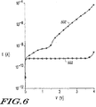
図6を参照すると、図2または図3に詳細が示されるようなRPWTクランプの直流(DC)リーク電流曲線501(中抜きの円)特性が、図1に詳細が示されるような先行技術によるクランプの別のDCリーク電流曲線502(中抜きの方形)特性と比較される形で示され、この図によって本発明の一の態様が分かる。縦軸はESD保護素子を流れるDCリーク電流をアンペアで示す。横軸は保護素子の両端に掛かる電圧をボルトで示す。 Referring to FIG. 6, the direct current (DC) leakage current curve 501 (hollow circle) characteristic of the RPWT clamp as detailed in FIG. 2 or FIG. 3 is according to the prior art as detailed in FIG. Shown in comparison with another DC leakage current curve 502 (open square) characteristic of the clamp, this figure shows one aspect of the present invention. The vertical axis indicates the DC leakage current flowing through the ESD protection element in amperes. The horizontal axis indicates the voltage applied to both ends of the protective element in volts.
直流リークテストを使用して、DC電圧がトランジスタのドレインを正電位とし、ソースを負電位としてこられの間に印加されるときにトランジスタのドレインからソースに流れるリーク電流を測定することができる。図6に示すように、図5に示すESD特性と同様なESD特性を維持しながら、RPWTクランプ501のDCリーク電流は先行技術によるフローティングボディ型クランプ502のリーク電流よりもはるかに小さいことが分
かる。
A DC leakage test can be used to measure the leakage current that flows from the drain of a transistor to the source when a DC voltage is applied while the drain of the transistor is at a positive potential and the source is at a negative potential. As shown in FIG. 6, it can be seen that the DC leakage current of the
別の実施形態においては、本発明では、RPWTトランジスタのゲートをソースに接続する別の抵抗性素子を使用し、ゲート接続による効果を利用してESD保護を更に強化する。本発明は、低い接合電圧を利用して絶縁され、かつそのボディがそのソースに抵抗体を通して接続される構造のNMOSトランジスタにより形成されるRPWTNMOSトランジスタを含むことができる。更に本発明では、RPWTNMOSトランジスタを使用して、DCリーク電流を最小化し、かつラッチアップの発生を最大限防止しつつ、低電圧MOS素子をESDから保護することができる。 In another embodiment, the present invention uses another resistive element that connects the gate of the RPWT transistor to the source and takes advantage of the effect of the gate connection to further enhance ESD protection. The present invention may include an RPWT NMOS transistor formed by an NMOS transistor that is isolated utilizing a low junction voltage and whose body is connected to its source through a resistor. Furthermore, in the present invention, the RPWTMOS transistor can be used to protect the low voltage MOS device from ESD while minimizing the DC leakage current and preventing the occurrence of latch-up to the maximum.
本発明のRPWTトランジスタに使用する特定の製造プロセスはこの技術分野の当業者の技術レベルを用いて実施できるので、この製造プロセスによって記載の機能が実現する限りこの製造プロセスはここでは重要ではない。通常、本発明を実施する、または使用する場合、製造プロセスは先行技術から分かるように、必要な種々の設備及びエネルギー供給源、最終製品の予測される必要な適用形態、及び総合的な製造プロセスの必要性に基づいて選択することができる。 Since the specific manufacturing process used for the RPWT transistor of the present invention can be implemented using the level of skill of those skilled in the art, this manufacturing process is not critical here as long as the described function achieves the described function. In general, when implementing or using the present invention, the manufacturing process is, as can be seen from the prior art, the various equipment and energy sources required, the expected required application form of the final product, and the overall manufacturing process. You can choose based on your needs.
本明細書において使用する“a”または“an”という用語は、特に断らない限り、一つ、または一つよりも多い状態を指す。本明細書において使用する“substantially”という用語は、少なくとも所与の状態にほぼ近いことを意味する(例えば、好適には所与の状態の10%以内、更に好適には所与の状態の1%以内、そして最も好適には所与の状態の0.1%以内)。本明細書において使用する“another”という用語は、少なくとも2番目以降を意味する。本明細書において使用する“including”及び/又は“having”という用語は、“comprising”を意味する(すなわち、オープンランゲージ:権利範囲の解釈の場合、発明の本質を変更しない範囲で他の構成要件を含みうる用語)。本明細書において使用する“coupled”という用語は、必ずしも直接ではないが、そして必ずしも機械的ではないが、“connected”を意味する。 The terms “a” or “an” as used herein refer to one or more than one state unless otherwise specified. As used herein, the term “substantially” means at least approximately close to a given state (eg, preferably within 10% of a given state, more preferably 1 of a given state). Within 0.1%, and most preferably within 0.1% of a given condition). As used herein, the term “another” means at least a second or later. As used herein, the terms “including” and / or “having” mean “comprising” (ie, open language: in the interpretation of the scope of rights, other constituents may be used without changing the essence of the invention). Terminology). As used herein, the term “coupled” means “connected”, although not necessarily directly and not necessarily mechanically.
添付の請求項はmeans−plus−functionの制約(means−plus−functionの機能と当該開示された構造とを明確に関連付ける記載がない場合には、当該他の構造は米国特許法112条§6にいう「対応する」ものとは認められない」との判決による)を含むとは解釈されないものであると考える。本発明の構成の直下の構成を示す実施形態は添付の独立請求項及びこれらの請求項の等価物によって規定される。本発明の特定の実施形態は添付の従属請求項及びこれらの請求項の等価物によって差別化される。 The appended claims are a means-plus-function restriction (unless there is a statement associating the function of the means-plus-function with the disclosed structure clearly) It is considered that it is not construed to include “by the judgment that“ corresponding ”is not recognized”). Embodiments illustrating the structure immediately below the structure of the invention are defined by the appended independent claims and the equivalents of those claims. Particular embodiments of the present invention are differentiated by the appended dependent claims and their equivalents.
Claims (2)
基板と、
基板内の絶縁構造と、
絶縁構造に隣接する絶縁層と、
絶縁層及び絶縁構造に隣接するウェルと、
ウェル内の第1不純物領域と、
ボディを制御する第1不純物領域に隣接する第1電極取出し部と、
ウェル内の第2不純物領域と、
ソースを画定する第2不純物領域に隣接する第2電極取出し部と、前記ソースは接地に接続されていることと、
ウェルに隣接する誘電体層と、
ゲートを画定する誘電体層に隣接する第3電極取出し部と、
ウェル内の第3不純物領域と、
ドレインを画定する第3不純物領域に隣接する第4電極取出し部と、前記ドレインは保護されている回路のノードに接続されていることと、
第1電極取出し部と第2電極取出し部との間に接続される抵抗性素子とを備えるトランジスタ。A transistor configured to connect a resistor and a p-well;
A substrate,
An insulating structure in the substrate;
An insulating layer adjacent to the insulating structure;
A well adjacent to the insulating layer and the insulating structure;
A first impurity region in the well;
A first electrode extraction portion adjacent to a first impurity region for controlling the body;
A second impurity region in the well;
A second electrode extraction portion adjacent to a second impurity region defining the source; the source connected to ground;
A dielectric layer adjacent to the well;
A third electrode extraction portion adjacent to the dielectric layer defining the gate;
A third impurity region in the well;
A fourth electrode extraction portion adjacent to the third impurity region defining the drain; the drain connected to a node of the circuit being protected;
A transistor comprising a resistive element connected between a first electrode extraction portion and a second electrode extraction portion.
ドレインは入力/出力パッドに接続され、
ソースは接地端子に接続され、
ゲートはソースに接続され、
前記ボディの取り出し電極と前記ソースとの間に前記抵抗性素子を接続する、静電気保護回路。An electrostatic protection circuit for protecting a circuit having at least two terminals, wherein the first terminal is connected to an input / output pad and the second terminal is connected to a ground terminal. And a transistor configured to connect a p-well, the transistor including a resistive element made of the resistor, a gate, a body including the p-well, and a drain and a source having a conductivity type opposite to the p-well. Have
The drain is connected to the input / output pad,
The source is connected to the ground terminal,
The gate is connected to the source
An electrostatic protection circuit that connects the resistive element between an extraction electrode of the body and the source.
Applications Claiming Priority (2)
| Application Number | Priority Date | Filing Date | Title |
|---|---|---|---|
| US10/361,469 US6844597B2 (en) | 2003-02-10 | 2003-02-10 | Low voltage NMOS-based electrostatic discharge clamp |
| PCT/US2004/003094 WO2004073023A2 (en) | 2003-02-10 | 2004-02-04 | Low voltage nmos-based electrostatic discharge clamp |
Publications (3)
| Publication Number | Publication Date |
|---|---|
| JP2006517350A JP2006517350A (en) | 2006-07-20 |
| JP2006517350A5 JP2006517350A5 (en) | 2007-03-22 |
| JP4402109B2 true JP4402109B2 (en) | 2010-01-20 |
Family
ID=32824249
Family Applications (1)
| Application Number | Title | Priority Date | Filing Date |
|---|---|---|---|
| JP2006503295A Expired - Lifetime JP4402109B2 (en) | 2003-02-10 | 2004-02-04 | Low voltage NMOS type electrostatic discharge clamp |
Country Status (7)
| Country | Link |
|---|---|
| US (2) | US6844597B2 (en) |
| EP (1) | EP1595277A2 (en) |
| JP (1) | JP4402109B2 (en) |
| KR (1) | KR101006827B1 (en) |
| CN (1) | CN100416824C (en) |
| TW (1) | TWI322501B (en) |
| WO (1) | WO2004073023A2 (en) |
Families Citing this family (29)
| Publication number | Priority date | Publication date | Assignee | Title |
|---|---|---|---|---|
| JP2005311134A (en) * | 2004-04-22 | 2005-11-04 | Nec Electronics Corp | Electrostatic discharge protecting device |
| KR20060010979A (en) * | 2004-07-29 | 2006-02-03 | 현대자동차주식회사 | A remote monitoring and control system of vehicle and method thereof |
| US7122867B2 (en) * | 2004-11-19 | 2006-10-17 | United Microelectronics Corp. | Triple well structure and method for manufacturing the same |
| DE102005000801A1 (en) * | 2005-01-05 | 2006-07-13 | Infineon Technologies Ag | Device, arrangement and system for ESD protection |
| US7508038B1 (en) * | 2005-04-29 | 2009-03-24 | Zilog, Inc. | ESD protection transistor |
| US7394133B1 (en) * | 2005-08-31 | 2008-07-01 | National Semiconductor Corporation | Dual direction ESD clamp based on snapback NMOS cell with embedded SCR |
| US7268613B2 (en) * | 2005-10-31 | 2007-09-11 | International Business Machines Corporation | Transistor switch with integral body connection to prevent latchup |
| JP2008218564A (en) * | 2007-03-01 | 2008-09-18 | Matsushita Electric Ind Co Ltd | Semiconductor device |
| EP2150976A1 (en) * | 2007-04-27 | 2010-02-10 | Freescale Semiconductor, Inc. | Integrated circuit, electronic device and esd protection therefor |
| CN101373770B (en) * | 2007-08-20 | 2011-10-05 | 天津南大强芯半导体芯片设计有限公司 | Chip substrate electric potential isolating circuit and use thereof, and method for using the same |
| US8279566B2 (en) * | 2008-04-30 | 2012-10-02 | Freescale Semiconductor, Inc. | Multi-voltage electrostatic discharge protection |
| US20100067155A1 (en) | 2008-09-15 | 2010-03-18 | Altera Corporation | Method and apparatus for enhancing the triggering of an electrostatic discharge protection device |
| US8194370B2 (en) | 2008-11-25 | 2012-06-05 | Nuvoton Technology Corporation | Electrostatic discharge protection circuit and device |
| US8399909B2 (en) | 2009-05-12 | 2013-03-19 | Osi Optoelectronics, Inc. | Tetra-lateral position sensing detector |
| DE102011109596B4 (en) | 2011-08-05 | 2018-05-09 | Austriamicrosystems Ag | Circuit arrangement for protection against electrostatic discharges |
| CN102646601B (en) * | 2012-04-19 | 2016-09-28 | 北京燕东微电子有限公司 | A kind of semiconductor structure and manufacture method thereof |
| US9257463B2 (en) * | 2012-05-31 | 2016-02-09 | Taiwan Semiconductor Manufacturing Company, Ltd. | Self-aligned implantation process for forming junction isolation regions |
| CN103280458B (en) * | 2013-05-17 | 2015-07-29 | 电子科技大学 | A kind of integrated circuit (IC) chip ESD protection MOS device |
| CN103887194A (en) * | 2013-05-23 | 2014-06-25 | 上海华力微电子有限公司 | Parallel test device |
| KR101847227B1 (en) | 2013-05-31 | 2018-04-10 | 매그나칩 반도체 유한회사 | Electrostatic discharge transistor |
| KR101975608B1 (en) | 2013-06-12 | 2019-05-08 | 매그나칩 반도체 유한회사 | Electrostatic discharge high voltage type transistor and electrostatic dscharge protection circuit thereof |
| KR102098663B1 (en) | 2013-10-11 | 2020-04-08 | 삼성전자주식회사 | Electrostatic discharge protection device |
| JP6349217B2 (en) * | 2014-09-29 | 2018-06-27 | 日立オートモティブシステムズ株式会社 | Electronic control unit |
| CN104392995B (en) * | 2014-10-30 | 2017-09-22 | 京东方科技集团股份有限公司 | A kind of transistor, drive circuit and its driving method, display device |
| US9997510B2 (en) * | 2015-09-09 | 2018-06-12 | Vanguard International Semiconductor Corporation | Semiconductor device layout structure |
| US10680435B2 (en) * | 2016-04-26 | 2020-06-09 | Intersil Americas LLC | Enhanced electrostatic discharge (ESD) clamp |
| US20200066709A1 (en) * | 2018-08-21 | 2020-02-27 | Mediatek Inc. | Semiconductor device having noise isolation between power regulator circuit and electrostatic discharge clamp circuit |
| US10896953B2 (en) * | 2019-04-12 | 2021-01-19 | Globalfoundries Inc. | Diode structures |
| JP7455016B2 (en) | 2020-07-15 | 2024-03-25 | ルネサスエレクトロニクス株式会社 | semiconductor equipment |
Family Cites Families (7)
| Publication number | Priority date | Publication date | Assignee | Title |
|---|---|---|---|---|
| DE69331807T2 (en) * | 1992-09-30 | 2002-09-26 | Vladimir Feingold | INTRAOCULAR LENS INSERTION SYSTEM |
| US5563525A (en) * | 1995-02-13 | 1996-10-08 | Taiwan Semiconductor Manufacturing Company Ltd | ESD protection device with FET circuit |
| US5686751A (en) * | 1996-06-28 | 1997-11-11 | Winbond Electronics Corp. | Electrostatic discharge protection circuit triggered by capacitive-coupling |
| CN1051171C (en) * | 1997-04-14 | 2000-04-05 | 世界先进积体电路股份有限公司 | Electrostatic protecting circuits for semiconductor device and structure thereof |
| US6013932A (en) * | 1998-01-07 | 2000-01-11 | Micron Technology, Inc. | Supply voltage reduction circuit for integrated circuit |
| US6329692B1 (en) * | 1998-11-30 | 2001-12-11 | Motorola Inc. | Circuit and method for reducing parasitic bipolar effects during eletrostatic discharges |
| US6329691B1 (en) * | 1999-12-13 | 2001-12-11 | Tower Semiconductor Ltd. | Device for protection of sensitive gate dielectrics of advanced non-volatile memory devices from damage due to plasma charging |
-
2003
- 2003-02-10 US US10/361,469 patent/US6844597B2/en not_active Expired - Lifetime
-
2004
- 2004-02-04 JP JP2006503295A patent/JP4402109B2/en not_active Expired - Lifetime
- 2004-02-04 CN CNB2004800038357A patent/CN100416824C/en not_active Expired - Lifetime
- 2004-02-04 KR KR1020057014761A patent/KR101006827B1/en active IP Right Grant
- 2004-02-04 EP EP04708128A patent/EP1595277A2/en not_active Withdrawn
- 2004-02-04 WO PCT/US2004/003094 patent/WO2004073023A2/en active Application Filing
- 2004-02-06 TW TW093102773A patent/TWI322501B/en not_active IP Right Cessation
- 2004-12-01 US US11/000,584 patent/US7288820B2/en not_active Expired - Lifetime
Also Published As
| Publication number | Publication date |
|---|---|
| JP2006517350A (en) | 2006-07-20 |
| WO2004073023A2 (en) | 2004-08-26 |
| KR20050107753A (en) | 2005-11-15 |
| TWI322501B (en) | 2010-03-21 |
| TW200417022A (en) | 2004-09-01 |
| US6844597B2 (en) | 2005-01-18 |
| CN1748309A (en) | 2006-03-15 |
| CN100416824C (en) | 2008-09-03 |
| EP1595277A2 (en) | 2005-11-16 |
| WO2004073023A3 (en) | 2004-12-23 |
| US20050093073A1 (en) | 2005-05-05 |
| US20040155300A1 (en) | 2004-08-12 |
| US7288820B2 (en) | 2007-10-30 |
| KR101006827B1 (en) | 2011-01-12 |
Similar Documents
| Publication | Publication Date | Title |
|---|---|---|
| JP4402109B2 (en) | Low voltage NMOS type electrostatic discharge clamp | |
| US7187527B2 (en) | Electrostatic discharge conduction device and mixed power integrated circuits using same | |
| KR100517770B1 (en) | Electrostatic Discharge Protection Element | |
| US20080055805A1 (en) | Semiconductor device having electro static discharge detection circuit | |
| US7576961B2 (en) | Electrostatic discharge protection circuit using triple welled silicon controlled rectifier | |
| JPH08222643A (en) | Input protective circuit for semiconductor device | |
| KR100387189B1 (en) | Semiconductor device on insulator and its protection circuit | |
| US20030043517A1 (en) | Electro-static discharge protecting circuit | |
| JP3559075B2 (en) | Polarity reversal protection device for integrated electronic circuits in CMOS technology | |
| US8384124B2 (en) | Semiconductor device and semiconductor integrated circuit device for driving plasma display using the semiconductor device | |
| KR20180058432A (en) | Esd protection circuit | |
| KR100357191B1 (en) | ESD protection circuit using metal coupling capacitor | |
| KR100907894B1 (en) | Electrostatic Discharge Protection Circuit | |
| JP2008172216A (en) | Well potential triggered esd protection | |
| KR100608437B1 (en) | ESD protection circuit using diode | |
| JP2650276B2 (en) | Semiconductor integrated circuit device | |
| KR100652314B1 (en) | Esd protection circuit | |
| JP2005513782A (en) | Polarity reversal allowable electric circuit for ESD protection | |
| KR100253585B1 (en) | Semiconductor device for electrostatic discharge protecting | |
| KR100613055B1 (en) | Electrostatic discharge protection circuit in a semiconductor | |
| KR101369194B1 (en) | Esd protection circuit for semiconductor integrated circuit | |
| KR100713923B1 (en) | Electrostatic protection device for semiconductor circuit | |
| KR100329074B1 (en) | Semiconductor device | |
| KR100329073B1 (en) | Semiconductor device | |
| KR20100085226A (en) | Floating body ggnmos |
Legal Events
| Date | Code | Title | Description |
|---|---|---|---|
| A521 | Request for written amendment filed |
Free format text: JAPANESE INTERMEDIATE CODE: A523 Effective date: 20070202 |
|
| A621 | Written request for application examination |
Free format text: JAPANESE INTERMEDIATE CODE: A621 Effective date: 20070202 |
|
| A131 | Notification of reasons for refusal |
Free format text: JAPANESE INTERMEDIATE CODE: A131 Effective date: 20090217 |
|
| A977 | Report on retrieval |
Free format text: JAPANESE INTERMEDIATE CODE: A971007 Effective date: 20090219 |
|
| A521 | Request for written amendment filed |
Free format text: JAPANESE INTERMEDIATE CODE: A523 Effective date: 20090518 |
|
| A131 | Notification of reasons for refusal |
Free format text: JAPANESE INTERMEDIATE CODE: A131 Effective date: 20090616 |
|
| A521 | Request for written amendment filed |
Free format text: JAPANESE INTERMEDIATE CODE: A523 Effective date: 20090701 |
|
| TRDD | Decision of grant or rejection written | ||
| A01 | Written decision to grant a patent or to grant a registration (utility model) |
Free format text: JAPANESE INTERMEDIATE CODE: A01 Effective date: 20091006 |
|
| A01 | Written decision to grant a patent or to grant a registration (utility model) |
Free format text: JAPANESE INTERMEDIATE CODE: A01 |
|
| A61 | First payment of annual fees (during grant procedure) |
Free format text: JAPANESE INTERMEDIATE CODE: A61 Effective date: 20091028 |
|
| R150 | Certificate of patent or registration of utility model |
Ref document number: 4402109 Country of ref document: JP Free format text: JAPANESE INTERMEDIATE CODE: R150 Free format text: JAPANESE INTERMEDIATE CODE: R150 |
|
| FPAY | Renewal fee payment (event date is renewal date of database) |
Free format text: PAYMENT UNTIL: 20121106 Year of fee payment: 3 |
|
| FPAY | Renewal fee payment (event date is renewal date of database) |
Free format text: PAYMENT UNTIL: 20121106 Year of fee payment: 3 |
|
| FPAY | Renewal fee payment (event date is renewal date of database) |
Free format text: PAYMENT UNTIL: 20131106 Year of fee payment: 4 |
|
| R250 | Receipt of annual fees |
Free format text: JAPANESE INTERMEDIATE CODE: R250 |
|
| R250 | Receipt of annual fees |
Free format text: JAPANESE INTERMEDIATE CODE: R250 |
|
| R250 | Receipt of annual fees |
Free format text: JAPANESE INTERMEDIATE CODE: R250 |
|
| R250 | Receipt of annual fees |
Free format text: JAPANESE INTERMEDIATE CODE: R250 |
|
| R250 | Receipt of annual fees |
Free format text: JAPANESE INTERMEDIATE CODE: R250 |
|
| S533 | Written request for registration of change of name |
Free format text: JAPANESE INTERMEDIATE CODE: R313533 |
|
| R250 | Receipt of annual fees |
Free format text: JAPANESE INTERMEDIATE CODE: R250 |
|
| R350 | Written notification of registration of transfer |
Free format text: JAPANESE INTERMEDIATE CODE: R350 |
|
| R250 | Receipt of annual fees |
Free format text: JAPANESE INTERMEDIATE CODE: R250 |
|
| R250 | Receipt of annual fees |
Free format text: JAPANESE INTERMEDIATE CODE: R250 |
|
| R250 | Receipt of annual fees |
Free format text: JAPANESE INTERMEDIATE CODE: R250 |
|
| R250 | Receipt of annual fees |
Free format text: JAPANESE INTERMEDIATE CODE: R250 |
|
| R250 | Receipt of annual fees |
Free format text: JAPANESE INTERMEDIATE CODE: R250 |
|
| R250 | Receipt of annual fees |
Free format text: JAPANESE INTERMEDIATE CODE: R250 |