JP4388429B2 - Resist underlayer film material and pattern forming method - Google Patents
Resist underlayer film material and pattern forming method Download PDFInfo
- Publication number
- JP4388429B2 JP4388429B2 JP2004212005A JP2004212005A JP4388429B2 JP 4388429 B2 JP4388429 B2 JP 4388429B2 JP 2004212005 A JP2004212005 A JP 2004212005A JP 2004212005 A JP2004212005 A JP 2004212005A JP 4388429 B2 JP4388429 B2 JP 4388429B2
- Authority
- JP
- Japan
- Prior art keywords
- group
- resist
- film
- derivatives
- underlayer film
- Prior art date
- Legal status (The legal status is an assumption and is not a legal conclusion. Google has not performed a legal analysis and makes no representation as to the accuracy of the status listed.)
- Active
Links
- 0 C*(C)(*)CC(C1)C2C(CC(C(F)(F)F)(C(F)(F)F)O)CC1C2 Chemical compound C*(C)(*)CC(C1)C2C(CC(C(F)(F)F)(C(F)(F)F)O)CC1C2 0.000 description 1
- KXVLSLKTHZGJJR-UHFFFAOYSA-N CC(C)(C)OC(C1C(CC2)CC2C1)O Chemical compound CC(C)(C)OC(C1C(CC2)CC2C1)O KXVLSLKTHZGJJR-UHFFFAOYSA-N 0.000 description 1
Images


Description
本発明は、半導体素子などの製造工程における微細加工に用いられる反射防止膜材料として有効なレジスト下層膜材料に関し、特に、遠紫外線、KrFエキシマレーザー光(248nm)、ArFエキシマレーザー光(193nm)、F2レーザー光(157nm)、Kr2レーザー光(146nm)、Ar2レーザー光(126nm)等での露光に好適な多層レジスト膜のレジスト下層膜材料に関する。さらに、本発明は、これを用いてリソグラフィーにより基板にパターンを形成する方法に関する。 The present invention relates to a resist underlayer film material that is effective as an antireflection film material used for microfabrication in a manufacturing process of a semiconductor element or the like, and in particular, far ultraviolet light, KrF excimer laser light (248 nm), ArF excimer laser light (193 nm), The present invention relates to a resist underlayer film material of a multilayer resist film suitable for exposure with F 2 laser light (157 nm), Kr 2 laser light (146 nm), Ar 2 laser light (126 nm), or the like. Furthermore, this invention relates to the method of forming a pattern in a board | substrate by lithography using this.
近年、LSIの高集積化と高速度化に伴い、パターンルールの微細化が求められている中、現在汎用技術として用いられている光露光を用いたリソグラフィーにおいては、光源の波長に由来する本質的な解像度の限界に近づきつつある。 In recent years, with the increasing integration and speed of LSIs, there is a need for finer pattern rules. In lithography using light exposure, which is currently used as a general-purpose technology, the essence derived from the wavelength of the light source The resolution limit is approaching.
レジストパターン形成の際に使用するリソグラフィー用の光源として、水銀灯のg線(436nm)もしくはi線(365nm)を光源とする光露光が広く用いられているが、更なる微細化のための手段として、露光光を短波長化する方法が有効とされてきた。このため、例えば64MビットDRAM加工方法の量産プロセスには、露光光源としてi線(365nm)に代わって短波長のKrFエキシマレーザー(248nm)が利用されている。しかし、更に微細な加工技術(例えば、加工寸法が0.13μm以下)を必要とする集積度1G以上のDRAMの製造には、より短波長の光源が必要とされ、特にArFエキシマレーザー(193nm)を用いたリソグラフィーが検討されてきている。 As a light source for lithography used in forming a resist pattern, light exposure using a g-ray (436 nm) or i-line (365 nm) of a mercury lamp as a light source is widely used, but as a means for further miniaturization. A method of shortening the wavelength of exposure light has been considered effective. For this reason, for example, in a mass production process of a 64-Mbit DRAM processing method, a short wavelength KrF excimer laser (248 nm) is used as an exposure light source instead of i-line (365 nm). However, in order to manufacture a DRAM having a degree of integration of 1G or more, which requires a finer processing technique (for example, a processing dimension of 0.13 μm or less), a light source with a shorter wavelength is required, particularly an ArF excimer laser (193 nm). Lithography using a material has been studied.
一方、従来、段差基板上に高アスペクト比のパターンを形成するには、例えば2層レジストプロセスのような多層レジストプロセスが優れていることが知られている。2層レジストプロセスにおいて、2層レジスト膜を一般的なアルカリ現像液で現像するためには、レジスト上層膜としてヒドロキシ基やカルボキシル基等の親水基を有する高分子シリコーン化合物を用いるのが好適であるとされている。 On the other hand, it is conventionally known that a multilayer resist process such as a two-layer resist process is excellent for forming a pattern with a high aspect ratio on a stepped substrate. In the two-layer resist process, in order to develop the two-layer resist film with a general alkaline developer, it is preferable to use a high molecular silicone compound having a hydrophilic group such as a hydroxy group or a carboxyl group as the resist upper layer film. It is said that.
このような高分子シリコーン化合物としては、KrFエキシマレーザー用として、安定なアルカリ可溶性シリコーンポリマーであるポリヒドロキシベンジルシルセスキオキサンのフェノール性水酸基の一部をt−Boc基で保護したものをベース樹脂として使用し、これと酸発生剤とを組み合わせたシリコーン系化学増幅ポジ型レジスト材料が提案されている(例えば、特許文献1、非特許文献1参照。)。また、ArFエキシマレーザー用としては、シクロヘキシルカルボン酸を酸不安定基で置換したタイプのシルセスキオキサンをベースにしたポジ型レジストが提案されている(例えば、特許文献2、特許文献3、非特許文献2参照。)。更に、F2レーザー用としては、ヘキサフルオロイソプロパノールを溶解性基として持つシルセスキオキサンをベースにしたポジ型レジストが提案されている(例えば、特許文献4参照。)。上記ポリマーは、トリアルコキシシシラン、又はトリハロゲン化シランの縮重合によるラダー骨格を含むポリシルセスキオキサンを主鎖に含むものである。
As such a high molecular silicone compound, a base resin in which a part of the phenolic hydroxyl group of polyhydroxybenzylsilsesquioxane, which is a stable alkali-soluble silicone polymer, is protected with a t-Boc group is used for a KrF excimer laser. A silicone-based chemically amplified positive resist material that is used in combination with an acid generator has been proposed (see, for example,
珪素が側鎖にペンダントされた高分子シリコーン化合物としては、珪素含有(メタ)アクリルエステル系ポリマーが提案されている(例えば、特許文献5、非特許文献3参照。)。 As a high molecular silicone compound in which silicon is pendant on a side chain, a silicon-containing (meth) acrylic ester-based polymer has been proposed (see, for example, Patent Document 5 and Non-Patent Document 3).
2層レジストプロセスに用いるレジスト下層膜としては、例えば酸素ガスによるエッチングが可能な炭化水素化合物等を挙げることができ、更にその下の基板をエッチングする場合におけるマスクになるため、基板エッチング時には高いエッチング耐性を有することが望ましい。レジスト上層膜をマスクにしたレジスト下層膜のエッチングが、酸素ガスエッチングによる場合は、レジスト下層膜は珪素原子を含まない炭化水素のみで構成されるのが望ましい。また、珪素原子を含有したレジスト上層膜の線幅制御性を向上させ、定在波によるパターン側壁の凹凸とパターンの崩壊を低減させるためには、レジスト下層膜は、反射防止膜としての機能も有し、具体的には、レジスト下層膜からレジスト上層膜内への反射率を1%以下に抑えることができるのが望ましい。 As the resist underlayer film used in the two-layer resist process, for example, a hydrocarbon compound that can be etched with oxygen gas, and the like can be used. Further, since it serves as a mask when etching the substrate underneath, high etching is performed during substrate etching. It is desirable to have resistance. When the etching of the resist lower layer film using the resist upper layer film as a mask is based on oxygen gas etching, the resist lower layer film is preferably composed only of hydrocarbons not containing silicon atoms. In addition, in order to improve the line width controllability of the resist upper layer film containing silicon atoms and to reduce the pattern sidewall irregularities and pattern collapse due to standing waves, the resist underlayer film also functions as an antireflection film. Specifically, it is desirable that the reflectance from the resist lower layer film into the resist upper layer film can be suppressed to 1% or less.
ところで、単層レジストプロセス用の下地反射防止膜は、その下の基板がポリシリコンやアルミニウムなどの高反射基板の場合でも、最適な屈折率(n値)、消光係数(k値)の材料を適切な膜厚に設定することによって、基板からの反射を1%以下に低減でき、極めて大きな反射防止効果を発揮することができる。 By the way, the base antireflection film for the single layer resist process is made of a material having an optimum refractive index (n value) and extinction coefficient (k value) even when the underlying substrate is a highly reflective substrate such as polysilicon or aluminum. By setting the film thickness to an appropriate thickness, the reflection from the substrate can be reduced to 1% or less, and an extremely large antireflection effect can be exhibited.
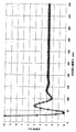
図1は、波長193nmにおける単層レジストプロセス用の下地反射防止膜の膜厚と反射率の関係を示すグラフである。図1から、例えば、波長193nmにおいて、レジスト膜の屈折率が1.7として、その下の反射防止膜の屈折率(屈折率の実数部)nが1.5、消光係数(屈折率の虚数部)kが0.5、膜厚が42nmであれば、反射率が0.5%以下になることが判る。 FIG. 1 is a graph showing the relationship between the film thickness and reflectance of a base antireflection film for a single layer resist process at a wavelength of 193 nm. From FIG. 1, for example, at a wavelength of 193 nm, the refractive index of the resist film is 1.7, the refractive index (real part of the refractive index) n of the underlying antireflection film is 1.5, and the extinction coefficient (imaginary number of refractive index). Part) When k is 0.5 and the film thickness is 42 nm, it can be seen that the reflectance is 0.5% or less.
しかし、下地基板に段差がある場合は、段差上で反射防止膜の膜厚が大きく変動する。図1を見て判るように、下地反射防止膜の反射防止効果は、光の吸収だけでなく、最適な膜厚を設定することによる干渉効果も利用しているため、干渉効果が強い40〜45nmの第一底辺はそれだけ反射防止効果も高いが、膜厚の変動によって大きく反射率が変動する。 However, when there is a step in the base substrate, the film thickness of the antireflection film varies greatly on the step. As can be seen from FIG. 1, the antireflection effect of the base antireflection film not only absorbs light but also uses an interference effect by setting an optimum film thickness, so that the interference effect is strong. The first bottom of 45 nm also has a high antireflection effect, but the reflectivity varies greatly with the change in film thickness.
そこで、反射防止膜材料に用いるベース樹脂の分子量を上げて段差上での膜厚変動を抑えコンフォーマル性を高めた材料が提案されている(例えば、特許文献6参照。)。しかし、この場合、ベース樹脂の分子量が高くなると、スピンコート後にピンホールが発生し易くなるといった問題や、濾過できなくなるといった問題、更には経時的に粘度変動が生じて膜厚が変化するといった問題や、ノズルの先端に結晶物が析出するといった問題が生じる。しかも、コンフォーマル性が発揮できるのは比較的高さの低い段差に限定される。 Thus, a material has been proposed in which the molecular weight of the base resin used for the antireflection film material is increased to suppress the film thickness fluctuation on the step and to improve the conformality (for example, see Patent Document 6). However, in this case, if the molecular weight of the base resin is high, problems such as pinholes are likely to occur after spin coating, filtration is impossible, and the film thickness changes due to changes in viscosity over time. In addition, there arises a problem that crystals are deposited at the tip of the nozzle. In addition, conformal properties can be exhibited only at steps having a relatively low height.
そこで次に、図1から膜厚変動による反射率の変動が比較的小さい第3底辺以上の膜厚(170nm以上)を採用する方法が考えられる。この場合、反射防止膜のk値が0.2〜0.3の間で、膜厚が170nm以上であれば、膜厚の変化に対する反射率の変動が小さく、しかも反射率を1.5%以下に抑えることができることが知られている。しかしながら、その上のレジスト膜のエッチング負荷を考えると、反射防止膜の厚膜化は限界があり、せいぜい100nm程度以下の第2底辺程度の厚膜化が限界である。 Then, from FIG. 1, a method of adopting a film thickness (170 nm or more) of the third base or more in which the change in reflectance due to the film thickness change is relatively small can be considered. In this case, if the k value of the antireflection film is between 0.2 and 0.3 and the film thickness is 170 nm or more, the change in the reflectivity with respect to the change in the film thickness is small, and the reflectivity is 1.5%. It is known that the following can be suppressed. However, considering the etching load of the resist film thereon, there is a limit to increasing the thickness of the antireflection film, and it is limiting to increase the thickness of the second bottom side of about 100 nm or less.
また、反射防止膜の下地が酸化膜や窒化膜などの透明膜で、更にその透明膜の下に段差がある場合、透明膜の表面がCMP(化学的機械研磨;Chemical Mechanical Polishing)などで平坦化されていたとしても、透明膜の膜厚が変動する。この場合、その上の反射防止膜の膜厚は一定にすることは可能であるが、反射防止膜の下の透明膜の膜厚が変動すると最低反射率となる膜の厚みが透明膜の膜厚分だけずれることになる。反射防止膜の膜厚を、下地が反射膜の時の最低反射率となる膜厚に設定しても、透明膜の膜厚変動によって反射率が高くなる場合がある。 When the base of the antireflection film is a transparent film such as an oxide film or a nitride film, and there is a step under the transparent film, the surface of the transparent film is flattened by CMP (Chemical Mechanical Polishing) or the like. Even if the thickness is changed, the thickness of the transparent film varies. In this case, it is possible to make the film thickness of the antireflection film constant on the film, but when the film thickness of the transparent film under the antireflection film varies, the film thickness that provides the minimum reflectance is the film of the transparent film. It will shift by the thickness. Even when the film thickness of the antireflection film is set to a film thickness that provides the minimum reflectance when the base is a reflection film, the reflectance may increase due to a change in the film thickness of the transparent film.
このような反射防止膜の材料は、無機系と有機系に大別できる。
無機系はSiON膜が挙げられる。これは、シランとアンモニアの混合ガスによるCVD(化学気相成長;Chemical Vapor Deposition)などで形成され、レジスト膜に対するエッチング選択比が大きいため、レジストへのエッチングの負荷が小さい利点があるが、剥離が困難なため、適用できる場合に制限がある。また、窒素原子を含む塩基性基板であるため、ポジレジストではフッティング、ネガレジストではアンダーカットプロファイルになり易いという欠点もある。
Such antireflection film materials can be broadly classified into inorganic and organic materials.
An inorganic system is a SiON film. This is formed by CVD (Chemical Vapor Deposition) using a mixed gas of silane and ammonia and has a large etching selection ratio with respect to the resist film. However, there are limitations when applicable. In addition, since it is a basic substrate containing nitrogen atoms, there is a drawback that it tends to have a footing in a positive resist and an undercut profile in a negative resist.
有機系は、スピンコート可能でCVDやスパッタリングなどの特別な装置を必要としない点、レジスト膜と同時に剥離可能な点、裾引き等の発生がなく、形状が素直で、レジスト膜との接着性も良好である点が利点であり、多くの有機材料をベースとした反射防止膜が提案された。例えば、ジフェニルアミン誘導体とホルムアルデヒド変性メラミン樹脂との縮合体、アルカリ可溶性樹脂と吸光剤とからなるもの(例えば、特許文献7参照。)や、無水マレイン酸共重合体とジアミン型吸光剤の反応物(例えば、特許文献8参照。)、樹脂バインダーとメチロールメラミン系熱架橋剤を含有するもの(例えば、特許文献9参照。)、カルボン酸基とエポキシ基と吸光基を同一分子内に有するアクリル樹脂ベース型(例えば、特許文献10参照。)、メチロールメラミンとベンゾフェノン系吸光剤からなるもの(例えば、特許文献11参照。)、ポリビニルアルコール樹脂に低分子吸光剤を添加したもの(例えば、特許文献12参照。)等が挙げられる。これらのすべての有機材料をベースとした反射防止膜は、バインダーポリマーに吸光剤を添加、あるいはポリマーに置換基として導入する方法をとっている。しかし、吸光剤の多くが芳香族基、あるいは2重結合を有するため、吸光剤の添加によってドライエッチング耐性が高まり、レジスト膜とのドライエッチング選択比がそれほど高くないという欠点がある。微細化が進行し、レジスト膜の薄膜化にも拍車がかかっており、更に次世代のArF露光においては、レジスト膜材料にアクリル又は脂環族のポリマーを使うことになるため、レジスト膜のエッチング耐性が低下する。更に、前述の通り、反射防止膜の膜厚を厚くしなければならないという問題もある。このため、エッチングは深刻な問題であり、レジスト膜に対してエッチング選択比の高い、即ち、エッチングスピードが速い反射防止膜が求められている。 Organic systems can be spin-coated and do not require special equipment such as CVD or sputtering, can be peeled off simultaneously with the resist film, have no tailing, have a straight shape, and adhere to the resist film The anti-reflection film based on many organic materials has been proposed. For example, a condensate of a diphenylamine derivative and a formaldehyde-modified melamine resin, an alkali-soluble resin and a light absorber (see, for example, Patent Document 7), a reaction product of a maleic anhydride copolymer and a diamine type light absorber ( For example, see Patent Document 8), an acrylic resin base containing a resin binder and a methylolmelamine-based thermal crosslinking agent (see, for example, Patent Document 9), a carboxylic acid group, an epoxy group, and a light-absorbing group in the same molecule. Type (for example, see Patent Document 10), one comprising methylol melamine and a benzophenone-based light absorber (for example, see Patent Document 11), or one obtained by adding a low molecular light absorber to a polyvinyl alcohol resin (for example, see Patent Document 12). Etc.). Antireflection films based on all these organic materials employ a method in which a light absorber is added to the binder polymer or introduced as a substituent into the polymer. However, since many of the light-absorbing agents have aromatic groups or double bonds, the addition of the light-absorbing agent increases the resistance to dry etching and has a drawback that the dry etching selectivity with the resist film is not so high. Since the miniaturization has progressed and the thinning of the resist film has been spurred, and in the next-generation ArF exposure, an acrylic or alicyclic polymer is used as the resist film material, so the resist film is etched. Resistance is reduced. Further, as described above, there is a problem that the thickness of the antireflection film must be increased. For this reason, etching is a serious problem, and an antireflection film having a high etching selectivity relative to a resist film, that is, a high etching speed is required.
一方、2層レジストプロセス用のレジスト下層膜における反射防止膜として要求される機能は、単層レジストプロセス用の反射防止膜のものとは異なっている。2層レジストプロセス用のレジスト下層膜は、基板をエッチングするときのマスクとなるため、基板エッチングの条件で高いエッチング耐性を有しなければならない。このように、単層レジストプロセスにおける反射防止膜には、単層レジスト膜のエッチング負荷を軽くするために早いエッチング速度が要求されるのに対して、逆の特性が要求される。また、基板エッチング時に十分なエッチング耐性を確保するため、レジスト下層膜の膜厚は単層レジスト膜と同等程度又はそれ以上の300nm以上にまで厚くしなければならない。ただ、300nm以上の膜厚では、膜厚の変化による反射率の変動はほぼ収束し、位相差制御による反射防止効果は期待できない。 On the other hand, the function required as an antireflection film in the resist underlayer film for the two-layer resist process is different from that of the antireflection film for the single-layer resist process. Since the resist underlayer film for the two-layer resist process serves as a mask for etching the substrate, it must have high etching resistance under the substrate etching conditions. As described above, the antireflection film in the single-layer resist process is required to have a high etching rate in order to lighten the etching load of the single-layer resist film, whereas the reverse characteristics are required. In addition, in order to ensure sufficient etching resistance during substrate etching, the thickness of the resist underlayer film must be increased to about 300 nm, which is equal to or higher than that of the single-layer resist film. However, when the film thickness is 300 nm or more, the change in reflectance due to the change in film thickness almost converges, and the antireflection effect by phase difference control cannot be expected.
ここで、レジスト下層膜の膜厚を0〜500nmの範囲で変動させた時の基板反射率を計算した結果を図2、3に示す。露光波長を193nm、レジスト上層膜のn値を1.74、k値を0.02と仮定している。
図2にはレジスト下層膜のk値を0.3に固定し、縦軸をn値、横軸を膜厚として、n値を1.0〜2.0の範囲、膜厚を0〜500nmの範囲で変動させたときの基板反射率を示す。図2を見ると、膜厚が300nm以上の2層レジストプロセス用のレジスト下層膜を想定した場合、n値が、レジスト上層膜と同程度かあるいはそれよりも少し高い1.6〜1.9の範囲で反射率を1%以下にできる最適値が存在することが判る。
Here, the results of calculating the substrate reflectivity when the thickness of the resist underlayer film is varied in the range of 0 to 500 nm are shown in FIGS. It is assumed that the exposure wavelength is 193 nm, the n value of the resist upper layer film is 1.74, and the k value is 0.02.
In FIG. 2, the k value of the resist underlayer film is fixed at 0.3, the vertical axis is the n value, the horizontal axis is the film thickness, the n value is in the range of 1.0 to 2.0, and the film thickness is 0 to 500 nm. The substrate reflectivity when it is varied in the range is shown. Referring to FIG. 2, assuming a resist underlayer film for a two-layer resist process having a film thickness of 300 nm or more, the n value is about 1.6 to 1.9 which is the same as or slightly higher than the resist upper layer film. It can be seen that there exists an optimum value that can reduce the reflectance to 1% or less in the range of.
図3には、レジスト下層膜のn値を1.5に固定し、縦軸をk値、横軸を膜厚として、k値を0.1〜0.8の範囲、膜厚を0〜500nmの範囲で変動させたときの反射率を示す。図3を見ると、膜厚が300nm以上の2層レジストプロセス用のレジスト下層膜を想定した場合、k値が0.24〜0.15の範囲で反射率をほぼ1%以下にすることが可能であることが判る。一方、40nm程度の薄膜で用いられる単層レジストプロセス用の反射防止膜の最適k値は0.4〜0.5であり、300nm以上の2層レジストプロセス用レジスト下層膜の最適k値とは異なる。このように、2層レジストプロセス用レジスト下層膜では、より低いk値、即ちより高透明である必要があることが示されている。 In FIG. 3, the n value of the resist underlayer film is fixed to 1.5, the vertical axis is the k value, the horizontal axis is the film thickness, the k value is in the range of 0.1 to 0.8, and the film thickness is 0 to The reflectivity when varied in the range of 500 nm is shown. Referring to FIG. 3, assuming a resist underlayer film for a two-layer resist process having a film thickness of 300 nm or more, the reflectance may be reduced to approximately 1% or less in the range of k value from 0.24 to 0.15. It turns out that it is possible. On the other hand, the optimum k value of an antireflection film for a single layer resist process used for a thin film of about 40 nm is 0.4 to 0.5, and what is the optimum k value of a resist underlayer film for a two layer resist process of 300 nm or more. Different. Thus, it is shown that the resist underlayer film for a two-layer resist process needs to have a lower k value, that is, a higher transparency.
そこで、波長193nm用のレジスト下層膜材料として、ポリヒドロキシスチレンとアクリルの共重合体が検討されている(例えば、非特許文献4参照。)。ポリヒドロキシスチレンは波長193nmに非常に強い吸収を持ち、そのもの単独ではk値が0.6前後と高い値である。そこで、k値が殆ど0であるアクリルと共重合させることによって、k値を0.25前後に調整しているのである。 Therefore, a polyhydroxystyrene / acrylic copolymer has been studied as a resist underlayer film material for a wavelength of 193 nm (for example, see Non-Patent Document 4). Polyhydroxystyrene has very strong absorption at a wavelength of 193 nm, and the k value itself is a high value of around 0.6. Therefore, the k value is adjusted to around 0.25 by copolymerizing with acrylic whose k value is almost zero.
しかしながら、ポリヒドロキシスチレンに対して、アクリルの基板エッチングにおけるエッチング耐性は弱く、しかもk値を下げるためにかなりの割合のアクリルを共重合せざるを得ず、結果的に基板エッチング時のエッチング耐性はかなり低下する。エッチング耐性は、エッチング速度だけでなく、エッチング後の表面ラフネスの発生にも現れてくる。アクリルの共重合によってエッチング後の表面ラフネスの増大が深刻なほど顕著になっている。 However, with respect to polyhydroxystyrene, the etching resistance in acrylic substrate etching is weak, and in order to lower the k value, a considerable proportion of acrylic must be copolymerized. As a result, the etching resistance during substrate etching is low. It drops considerably. Etching resistance appears not only in the etching rate but also in the occurrence of surface roughness after etching. The increase in surface roughness after etching becomes more prominent as a result of acrylic copolymerization.
そこで、ベンゼン環よりも波長193nmにおける透明性が高く、エッチング耐性が高いものの一つにナフタレン環があり、これを用いることが提案されている。例えば、ナフタレン環、アントラセン環を有するレジスト下層膜が提案されている(例えば、特許文献13参照。)。しかしながら、ナフトール共縮合ノボラック樹脂、ポリビニルナフタレン樹脂のk値は0.3〜0.4の間であり、目標の0.1〜0.3の透明性には未達であり、所望の反射防止効果を得るには更に透明性を上げなくてはならない。また、ナフトール共縮合ノボラック樹脂、ポリビニルナフタレン樹脂の波長193nmにおけるn値は低く、本発明者らの測定した結果では、ナフトール共縮合ノボラック樹脂で1.4、ポリビニルナフタレン樹脂に至っては1.2であり、目標とする範囲には未達である。さらに、アセナフチレン重合体が提案されているが(例えば、特許文献14、特許文献15参照)、これは波長248nmに比べて波長193nmにおけるn値が低く、k値は高く、共に目標値には達していない。
このように、n値が高く、k値が低く透明でかつエッチング耐性が高いレジスト下層膜が求められている。
Therefore, a naphthalene ring is one of those having higher transparency at a wavelength of 193 nm and higher etching resistance than a benzene ring, and it has been proposed to use this. For example, a resist underlayer film having a naphthalene ring or an anthracene ring has been proposed (see, for example, Patent Document 13). However, the k value of naphthol co-condensed novolak resin and polyvinyl naphthalene resin is between 0.3 and 0.4, and the target transparency of 0.1 to 0.3 is not achieved, and the desired antireflection In order to obtain the effect, the transparency must be further increased. In addition, the n value at a wavelength of 193 nm of the naphthol co-condensed novolak resin and the polyvinyl naphthalene resin is low, and as a result of measurement by the present inventors, it is 1.4 for the naphthol co-condensed novolak resin and 1.2 for the polyvinyl naphthalene resin. Yes, the target range has not been achieved. Furthermore, although an acenaphthylene polymer has been proposed (see, for example, Patent Document 14 and Patent Document 15), this has a lower n value at a wavelength of 193 nm than that of a wavelength of 248 nm, a higher k value, and both reach the target value. Not.
Thus, there is a demand for a resist underlayer film having a high n value, a low k value, and transparency and high etching resistance.
本発明はこのような問題点に鑑みてなされたもので、例えばレジスト上層膜が珪素を含有するものといった多層レジストプロセス用、特には2層レジストプロセス用のレジスト下層膜材料であって、特に短波長の露光に対して、優れた反射防止膜として機能し、すなわちポリヒドロキシスチレン、クレゾールノボラック、ナフトールノボラックなどよりも透明性が高く、最適なn値、k値を有し、しかも基板加工におけるエッチング耐性に優れたレジスト下層膜材料、及びこれを用いてリソグラフィーにより基板にパターンを形成する方法を提供することを目的とする。 The present invention has been made in view of such problems, and is a resist underlayer film material for a multilayer resist process, for example, a resist upper layer film containing silicon, particularly for a two-layer resist process. It functions as an excellent anti-reflection film for wavelength exposure, that is, it is more transparent than polyhydroxystyrene, cresol novolak, naphthol novolak, etc., and has optimal n and k values, and etching in substrate processing An object of the present invention is to provide a resist underlayer film material having excellent resistance and a method of forming a pattern on a substrate by lithography using the resist underlayer film material.
本発明は、上記課題を解決するためになされたもので、リソグラフィーで用いられる多層レジスト膜のレジスト下層膜材料であって、少なくとも、アセナフチレン類の繰り返し単位と、置換又は非置換のヒドロキシ基を有する繰り返し単位とを共重合してなる重合体を含むものであることを特徴とするレジスト下層膜材料を提供する。 The present invention has been made to solve the above problems, and is a resist underlayer film material for a multilayer resist film used in lithography, which has at least a repeating unit of acenaphthylenes and a substituted or unsubstituted hydroxy group. that provides a resist underlayer film material characterized by a repeating unit is intended to include copolymerized formed by polymer.
そして、この場合、前記重合体が、下記一般式(1)で示される繰り返し単位を有するものであるのが好ましい。

このように、アセナフチレン類の繰り返し単位と、置換又は非置換のヒドロキシ基を有する繰り返し単位とを共重合してなる重合体、特には上記一般式(1)で示される繰り返し単位を有する重合体を含むレジスト下層膜材料は、特に短波長の露光に対して、優れた反射防止膜として機能し、すなわち透明性が高く、最適なn値、k値を有し、しかも基板加工時におけるエッチング耐性に優れたものである。 Thus, a polymer obtained by copolymerizing a repeating unit of acenaphthylenes and a repeating unit having a substituted or unsubstituted hydroxy group, particularly a polymer having a repeating unit represented by the general formula (1) above. The resist underlayer film material that is included functions as an excellent antireflection film, particularly for exposure at a short wavelength, that is, has high transparency, has an optimal n value, k value, and etching resistance during substrate processing. It is excellent.
そして、本発明のレジスト下層膜材料では、さらに有機溶剤、酸発生剤、架橋剤のうちいずれか1つ以上のものを含有するのが好ましい。 Then, a resist underlayer film material of the present invention, furthermore organic solvents, acid generators, have the preferred to contain any one or more ones of the cross-linking agent.
このように、上記本発明のレジスト下層膜材料が、さらに有機溶剤、架橋剤、酸発生剤のうちいずれか一つ以上のものを含有することで、該材料の基板等への塗布性を向上させたり、基板等への塗布後にベーク等により、レジスト下層膜内での架橋反応を促進することができる。従って、このようなレジスト下層膜は、膜厚均一性が良く、レジスト上層膜とのインターミキシングの恐れが少なく、レジスト上層膜への低分子成分の拡散が少ないものとなる。 Thus, the resist underlayer film material of the present invention further contains any one or more of an organic solvent, a crosslinking agent, and an acid generator, thereby improving the applicability of the material to a substrate or the like. The crosslinking reaction in the resist underlayer film can be promoted by baking or after applying to the substrate or the like. Therefore, such a resist underlayer film has good film thickness uniformity, is less likely to be intermixed with the resist upper layer film, and has low diffusion of low molecular components into the resist upper layer film.
さらに、本発明は、リソグラフィーにより基板にパターンを形成する方法であって、少なくとも、前記本発明のレジスト下層膜材料を用いてレジスト下層膜を基板上に形成し、該下層膜の上にフォトレジスト組成物のレジスト上層膜を形成して、多層レジスト膜とし、該多層レジスト膜のパターン回路領域を露光した後、現像液で現像してレジスト上層膜にレジストパターンを形成し、該パターンが形成されたレジスト上層膜をマスクにしてレジスト下層膜をエッチングし、さらにパターンが形成された多層レジスト膜をマスクにして基板をエッチングして基板にパターンを形成することを特徴とするパターン形成方法を提供する。 Furthermore, the present invention is a method of forming a pattern on a substrate by lithography, wherein at least a resist underlayer film is formed on the substrate using the resist underlayer film material of the present invention, and a photoresist is formed on the underlayer film. The resist upper layer film of the composition is formed to form a multilayer resist film, the pattern circuit region of the multilayer resist film is exposed, and then developed with a developing solution to form a resist pattern on the resist upper layer film. A pattern forming method is provided, in which a resist underlayer film is etched using a resist upper layer film as a mask, and a substrate is etched using a multilayer resist film having a pattern formed as a mask to form a pattern on the substrate. The
このように、本発明のレジスト下層膜材料を用いてリソグラフィーによりパターンを形成すれば、高精度で基板にパターンを形成することができる。 Thus, if a pattern is formed by lithography using the resist underlayer film material of the present invention, the pattern can be formed on the substrate with high accuracy.
前記レジスト上層膜として、珪素原子を含有したものを用い、前記レジスト上層膜をマスクにしたレジスト下層膜のエッチングを、酸素ガスを主体とするドライエッチングで行うのが好ましい。 Examples resist upper layer film, using a material obtained by containing a silicon atom, the resist etching of the upper film using the resist underlayer film as a mask, has the preferred to carry out the oxygen gas in the dry etching mainly.
このように、本発明のレジスト下層膜材料を用いて形成したレジスト下層膜は、レジスト上層膜として、珪素原子を含有したものを用い、レジスト上層膜をマスクにした下層膜のエッチングを、酸素ガスを主体とするドライエッチングで行うことでパターンを形成するのに特に適したものとなっている。従って、この多層レジスト膜をマスクにして基板をエッチングし、基板にパターンを形成すれば、高精度のパターンを形成することができる。 As described above, the resist underlayer film formed using the resist underlayer film material of the present invention uses a silicon atom-containing resist upper layer film, and etching of the lower layer film using the resist upper layer film as a mask is performed using oxygen gas. It is particularly suitable for forming a pattern by performing dry etching mainly composed of. Therefore, if the substrate is etched using the multilayer resist film as a mask and a pattern is formed on the substrate, a highly accurate pattern can be formed.
また、この場合、前記パターンが形成された多層レジスト膜をマスクにした基板のエッチングを、フロン系ガス、塩素系ガス、臭素系ガスのいずれかを主体とするドライエッチングで行うことができる。 In this case, the etching of the substrate in which the multi-layer resist film on which the pattern is formed on the mask, flon gas, chlorine gas, Ru can either bromine-based gas carried by dry etching mainly.
本発明のレジスト下層膜材料を用いて形成したレジスト下層膜は、フロン系ガス、塩素系ガス、臭素系ガスのいずれかを主体とするドライエッチングに対して、特にエッチング耐性に優れるものである。従って、この多層レジスト膜をマスクにして基板をエッチングするのに、フロン系ガス、塩素系ガス、臭素系ガスのいずれかを主体とするドライエッチングで基板にパターンを形成すれば、高精度のパターンを形成することができる。 The resist underlayer film formed by using the resist underlayer film material of the present invention is particularly excellent in etching resistance against dry etching mainly composed of any one of a fluorocarbon gas, a chlorine gas, and a bromine gas. Therefore, if the substrate is etched using this multilayer resist film as a mask, a pattern with high accuracy can be obtained by forming a pattern on the substrate by dry etching mainly using any of a fluorocarbon gas, a chlorine gas, or a bromine gas. Can be formed.
以上説明したように、本発明によれば、例えばレジスト上層膜が珪素を含有するものといった多層レジストプロセス用、特には2層レジストプロセス用のレジスト下層膜材料であって、特に短波長の露光に対して、優れた反射防止膜として機能し、すなわちポリヒドロキシスチレン、クレゾールノボラック、ナフトールノボラックなどよりも透明性が高く、最適なn値(屈折率)、k値(消光係数)を有し、しかも基板加工におけるエッチング耐性に優れたレジスト下層膜材料を得ることができる。 As described above, according to the present invention, for example, a resist underlayer film material for a multi-layer resist process such as one in which the resist upper layer film contains silicon, particularly for a two-layer resist process, particularly for exposure at a short wavelength. On the other hand, it functions as an excellent antireflection film, that is, it is more transparent than polyhydroxystyrene, cresol novolak, naphthol novolak, etc., and has an optimal n value (refractive index) and k value (quenching coefficient). A resist underlayer film material having excellent etching resistance in substrate processing can be obtained.
以下、本発明を実施するための最良の形態について説明するが、本発明はこれらに限定されるものではない。
本発明者らは、上記目的を達成するために鋭意検討を行った結果、アセナフチレン類の繰り返し単位と、置換又は非置換のヒドロキシ基を有する繰り返し単位とを共重合してなる重合体が、例えば波長193nmといった短波長の露光において、最適なn値、k値を有し、かつエッチング耐性にも優れ、珪素含有2層レジストプロセスといった多層レジストプロセス用レジスト下層膜として有望な材料であることを見出し、本発明をなすに至った。
Hereinafter, the best mode for carrying out the present invention will be described, but the present invention is not limited thereto.
As a result of intensive studies to achieve the above object, the present inventors have obtained a polymer obtained by copolymerizing a repeating unit of acenaphthylenes and a repeating unit having a substituted or unsubstituted hydroxy group, for example, It has been found that it is a promising material as a resist underlayer film for a multilayer resist process such as a silicon-containing two-layer resist process, having an optimum n value and k value in exposure at a short wavelength such as 193 nm and excellent etching resistance. The present invention has been made.
すなわち、本発明のレジスト下層膜材料は、リソグラフィーで用いられる多層レジスト膜のレジスト下層膜材料であって、少なくとも、アセナフチレン類の繰り返し単位と、置換又は非置換のヒドロキシ基を有する繰り返し単位とを共重合してなる重合体を含むものであることを特徴とする。 That is, the resist underlayer film material of the present invention is a resist underlayer film material of a multilayer resist film used in lithography, and includes at least a repeating unit of acenaphthylenes and a repeating unit having a substituted or unsubstituted hydroxy group. It is characterized by containing a polymer obtained by polymerization.
そして、この場合、前記重合体が、下記一般式(1)で示される繰り返し単位を有するものであるのが好ましい。
このような本発明のレジスト下層膜材料から形成したレジスト下層膜は、珪素含有2層レジストプロセス、珪素含有中間層を有する3層レジストプロセスといった多層レジストプロセスに適用可能な新規なレジスト下層膜である。特に、波長193nmといった短波長での露光において膜厚200nm以上とした時に反射防止効果に優れ、かつ基板エッチングの条件におけるエッチング耐性に優れるものである。 The resist underlayer film formed from the resist underlayer film material of the present invention is a novel resist underlayer film applicable to a multilayer resist process such as a silicon-containing two-layer resist process and a three-layer resist process having a silicon-containing intermediate layer. . In particular, when exposure is performed at a short wavelength such as 193 nm, the antireflection effect is excellent when the film thickness is 200 nm or more, and the etching resistance under substrate etching conditions is excellent.
また、レジスト下層膜材料に、さらに有機溶剤、架橋剤、酸発生剤のうちいずれか一つ以上のものを含有させることで、該材料の基板等への塗布性を向上させたり、基板等への塗布後にベーク等により、レジスト下層膜内での架橋反応を促進することができる。従って、このようなレジスト下層膜は、膜厚均一性が良く、レジスト上層膜とのインターミキシングの恐れが少なく、レジスト上層膜への低分子成分の拡散が少ないものとなる。 Further, by adding any one or more of an organic solvent, a crosslinking agent, and an acid generator to the resist underlayer film material, it is possible to improve the coating property of the material on the substrate or the like. The crosslinking reaction in the resist underlayer film can be promoted by baking or the like after coating. Therefore, such a resist underlayer film has good film thickness uniformity, is less likely to be intermixed with the resist upper layer film, and has low diffusion of low molecular components into the resist upper layer film.
ここで、本発明のレジスト下層膜材料に含まれる重合体中の繰り返し単位で、置換又は非置換のヒドロキシ基を有する繰り返し単位、特には一般式(1)で示される繰り返し単位a、bとしては、具体的には下記に例示することができる。 Here, as a repeating unit in the polymer contained in the resist underlayer film material of the present invention, a repeating unit having a substituted or unsubstituted hydroxy group, particularly the repeating units a and b represented by the general formula (1) Specifically, it can be exemplified below.
上記一般式(1)で示される繰り返し単位a、bを得るためのモノマーは、エチレン不飽和結合を有するものであり、またヒドロキシ基は重合時にはアセチル基やホルミル基、ピバロイル基、アセタール基、トリメチルシリル基などで置換されていてもよい。 The monomer for obtaining the repeating units a and b represented by the general formula (1) has an ethylenically unsaturated bond, and the hydroxy group is an acetyl group, a formyl group, a pivaloyl group, an acetal group, trimethylsilyl during polymerization. It may be substituted with a group or the like.
本発明のレジスト下層膜材料は、アセナフチレン類の繰り返し単位と、置換又は非置換のヒドロキシ基を有する繰り返し単位とを共重合してなる重合体をベースとするが、他のモノマーと共重合したものを用いることもできる。共重合可能なモノマーとしては、スチレン、インデン、インドール、メチレンインダン、(メタ)アクリル誘導体、ノルボルナジエン誘導体、ノルボルネン誘導体、無水マレイン酸、マレイミド誘導体、ビニルナフタレン誘導体、ビニルアントラセン誘導体、ビニルエーテル誘導体、アリルエーテル誘導体、(メタ)アクリロニトリル、ビニルピロリドン、テトラフルオロエチレンなどが挙げられ、これらのものを加えた3元以上の共重合体であっても構わない。 The resist underlayer film material of the present invention is based on a polymer obtained by copolymerizing a repeating unit of acenaphthylenes and a repeating unit having a substituted or unsubstituted hydroxy group, but is copolymerized with other monomers. Can also be used. Examples of copolymerizable monomers include styrene, indene, indole, methyleneindane, (meth) acryl derivatives, norbornadiene derivatives, norbornene derivatives, maleic anhydride, maleimide derivatives, vinyl naphthalene derivatives, vinyl anthracene derivatives, vinyl ether derivatives, allyl ether derivatives. , (Meth) acrylonitrile, vinyl pyrrolidone, tetrafluoroethylene, etc. may be mentioned, and a ternary or higher copolymer containing these may be used.
これら本発明のレジスト下層膜材料に含まれる重合体を合成するには、1つの方法としてはアセナフチレンとヒドロキシ基を有するモノマーを有機溶剤中、ラジカル開始剤あるいはカチオン重合開始剤を加え加熱重合を行う。ヒドロキシ基を含むモノマーのヒドロキシ基をアセチル基で置換させておき、得られた高分子化合物を有機溶剤中アルカリ加水分解を行い、アセチル基を脱保護することもできる。また、アセナフチレンとグリシジルエーテル基を有するモノマーと共重合した後、加水分解によってエポキシ環を開環させてアルコールにすることもできる。重合時に使用する有機溶剤としてはトルエン、ベンゼン、テトラヒドロフラン、ジエチルエーテル、ジオキサン等が例示できる。ラジカル重合開始剤としては、2,2´−アゾビスイソブチロニトリル(AIBN)、2,2´−アゾビス(2,4−ジメチルバレロニトリル)、ジメチル2,2−アゾビス(2−メチルプロピオネート)、ベンゾイルパーオキシド、ラウロイルパーオキシド等が例示でき、好ましくは50℃から80℃に加熱して重合できる。カチオン重合開始剤としては、硫酸、燐酸、塩酸、硝酸、次亜塩素酸、トリクロロ酢酸、トリフルオロ酢酸、メタンスルホン酸、トリフルオロメタンスルホン酸、カンファースルホン酸、トシル酸などの酸、BF3、AlCl3、TiCl4、SnCl4などのフリーデルクラフツ触媒のほか、I2、(C6H5)3CClのようにカチオンを生成しやすい物質が使用される。
In order to synthesize the polymer contained in the resist underlayer film material of the present invention, one method is to perform polymerization by adding acenaphthylene and a hydroxyl group-containing monomer in an organic solvent and adding a radical initiator or a cationic polymerization initiator. . The hydroxy group of the monomer containing a hydroxy group can be substituted with an acetyl group, and the resulting polymer compound can be subjected to alkaline hydrolysis in an organic solvent to deprotect the acetyl group. Moreover, after copolymerizing with the monomer which has acenaphthylene and a glycidyl ether group, an epoxy ring can be opened by hydrolysis and it can also be set as alcohol. Examples of the organic solvent used at the time of polymerization include toluene, benzene, tetrahydrofuran, diethyl ether, dioxane and the like. Examples of radical polymerization initiators include 2,2′-azobisisobutyronitrile (AIBN), 2,2′-azobis (2,4-dimethylvaleronitrile),
反応時間としては2〜100時間、好ましくは5〜20時間である。アルカリ加水分解時の塩基としては、アンモニア水、トリエチルアミン等が使用できる。また反応温度としては−20〜100℃、好ましくは0〜60℃であり、反応時間としては0.2〜100時間、好ましくは0.5〜20時間である。 The reaction time is 2 to 100 hours, preferably 5 to 20 hours. Ammonia water, triethylamine, etc. can be used as the base during the alkali hydrolysis. The reaction temperature is −20 to 100 ° C., preferably 0 to 60 ° C., and the reaction time is 0.2 to 100 hours, preferably 0.5 to 20 hours.
質量平均分子量は1,500〜200,000の範囲が好ましく、より好ましくは2,000〜100,000の範囲である。分子量分布は特に制限がなく、分画によって低分子体及び高分子体を除去し、分散度を小さくすることも可能であり、分子量、分散度が異なる2つ以上の一般式(1)の重合体の混合、あるいは組成比の異なる2種以上の一般式(1)の重合体を混合してもかまわない。 The mass average molecular weight is preferably in the range of 1,500 to 200,000, more preferably in the range of 2,000 to 100,000. The molecular weight distribution is not particularly limited, and low molecular weight and high molecular weight substances can be removed by fractionation to reduce the degree of dispersion. The weight of two or more general formulas (1) having different molecular weights and degrees of dispersion can be reduced. Mixtures of blends or two or more polymers of the general formula (1) having different composition ratios may be mixed.
本発明のレジスト下層膜材料に含まれる重合体、特には一般式(1)で示される繰り返し単位を有する重合体の波長193nmにおける透明性を更に向上させるために、水素添加を行うことができる。好ましい水素添加の割合は、芳香族基の80モル%以下、より好ましくは60モル%以下である。 In order to further improve the transparency of the polymer contained in the resist underlayer film material of the present invention, particularly the polymer having a repeating unit represented by the general formula (1) at a wavelength of 193 nm, hydrogenation can be performed. A preferable hydrogenation ratio is 80 mol% or less, more preferably 60 mol% or less of the aromatic group.
本発明のレジスト下層膜材料用のベース樹脂は、アセナフチレン類の繰り返し単位と、置換又は非置換のヒドロキシ基を有する繰り返し単位とを共重合してなる重合体を含むことを特徴とするが、前述の反射防止膜材料として挙げられている従来のポリマーとブレンドすることもできる。ポリアセナフチレンのガラス転移点は150℃以上であり、このもの単独ではビアホールなどの深いホールの埋め込み特性が劣る場合がある。ホールをボイドを発生させずに埋め込むためには、ガラス転移点の低いポリマーを用い、架橋温度よりも低い温度で熱フローさせながらホールの底にまで樹脂を埋め込む手法がとられる(例えば、特開2000−294504号公報参照。)。ガラス転移点の低いポリマー、特にガラス転移点が180℃以下、とりわけ100〜170℃のポリマー、例えばアクリル誘導体、ビニルアルコール、ビニルエーテル類、アリルエーテル類、スチレン誘導体、アリルベンゼン誘導体、エチレン、プロピレン、ブタジエンなどのオレフィン類から選ばれる1種あるいは2種以上の共重合ポリマー、メタセシス開環重合などによるポリマーとブレンドすることによってガラス転移点を低下させ、ビアホールの埋め込み特性を向上させることができる。 The base resin for the resist underlayer film material of the present invention includes a polymer obtained by copolymerizing a repeating unit of acenaphthylenes and a repeating unit having a substituted or unsubstituted hydroxy group. It can also be blended with conventional polymers mentioned as antireflective coating materials. Polyacenaphthylene has a glass transition point of 150 ° C. or higher, and this alone may have poor deep hole filling characteristics such as via holes. In order to embed holes without generating voids, a technique is employed in which a polymer having a low glass transition point is used and a resin is embedded to the bottom of the hole while heat-flowing at a temperature lower than the crosslinking temperature (for example, JP 2000-294504 gazette.) Polymers having a low glass transition point, especially polymers having a glass transition point of 180 ° C. or lower, particularly 100 to 170 ° C., such as acrylic derivatives, vinyl alcohol, vinyl ethers, allyl ethers, styrene derivatives, allylbenzene derivatives, ethylene, propylene, butadiene By blending with one or two or more types of copolymer selected from olefins such as metathesis ring-opening polymerization, the glass transition point can be lowered, and the via hole embedding property can be improved.
レジスト下層膜に要求される性能の一つとして、レジスト上層膜とのインターミキシングがないこと、レジスト上層膜ヘの低分子成分の拡散がないことが挙げられる(例えば、「Proc. SPIE Vol.2195、p225−229(1994)」参照。)。これらを防止するために、一般的にレジスト下層膜をスピンコート法などで基板に形成後、ベークで熱架橋するという方法がとられている。そのため、レジスト下層膜材料の成分として架橋剤を添加する場合、ポリマーに架橋性の置換基を導入するようにしてもよい。 One of the performances required for the resist underlayer film is that there is no intermixing with the resist upper layer film and that there is no diffusion of low molecular components into the resist upper layer film (for example, “Proc. SPIE Vol. 2195”). P225-229 (1994) ". In order to prevent these problems, a method is generally employed in which a resist underlayer film is formed on a substrate by spin coating or the like and then thermally crosslinked by baking. Therefore, when a crosslinking agent is added as a component of the resist underlayer film material, a crosslinkable substituent may be introduced into the polymer.
本発明で使用可能な架橋剤の具体例を列挙すると、メチロール基、アルコキシメチル基、アシロキシメチル基から選ばれる少なくとも一つの基で置換されたメラミン化合物、グアナミン化合物、グリコールウリル化合物又はウレア化合物、エポキシ化合物、イソシアネート化合物、アジド化合物、アルケニルエーテル基などの2重結合を含む化合物等を挙げることができる。これらは添加剤として用いてもよいが、ポリマー側鎖にペンダント基として導入してもよい。また、ヒドロキシ基を含む化合物も架橋剤として用いることができる。 Specific examples of the crosslinking agent that can be used in the present invention include a melamine compound, a guanamine compound, a glycoluril compound, or a urea compound substituted with at least one group selected from a methylol group, an alkoxymethyl group, and an acyloxymethyl group. Examples include compounds containing double bonds such as epoxy compounds, isocyanate compounds, azide compounds, and alkenyl ether groups. These may be used as additives, but may be introduced as pendant groups in the polymer side chain. A compound containing a hydroxy group can also be used as a crosslinking agent.
前記架橋剤の具体例のうち、さらにエポキシ化合物を例示すると、トリス(2,3−エポキシプロピル)イソシアヌレート、トリメチロールメタントリグリシジルエーテル、トリメチロールプロパントリグリシジルエーテル、トリエチロールエタントリグリシジルエーテルなどが例示される。メラミン化合物を具体的に例示すると、ヘキサメチロールメラミン、ヘキサメトキシメチルメラミン、ヘキサメチロールメラミンの1〜6個のメチロール基がメトキシメチル化した化合物及びその混合物、ヘキサメトキシエチルメラミン、ヘキサアシロキシメチルメラミン、ヘキサメチロールメラミンのメチロール基の1〜6個がアシロキシメチル化した化合物又はその混合物が挙げられる。グアナミン化合物としては、テトラメチロールグアナミン、テトラメトキシメチルグアナミン、テトラメチロールグアナミンの1〜4個のメチロール基がメトキシメチル化した化合物及びその混合物、テトラメトキシエチルグアナミン、テトラアシロキシグアナミン、テトラメチロールグアナミンの1〜4個のメチロール基がアシロキシメチル化した化合物及びその混合物が挙げられる。グリコールウリル化合物としては、テトラメチロールグリコールウリル、テトラメトキシグリコールウリル、テトラメトキシメチルグリコールウリル、テトラメチロールグリコールウリルのメチロール基の1〜4個がメトキシメチル基化した化合物、又はその混合物、テトラメチロールグリコールウリルのメチロール基の1〜4個がアシロキシメチル化した化合物又はその混合物が挙げられる。ウレア化合物としてはテトラメチロールウレア、テトラメトキシメチルウレア、テトラメチロールウレアの1〜4個のメチロール基がメトキシメチル基化した化合物又はその混合物、テトラメトキシエチルウレアなどが挙げられる。
イソシアネート化合物としては、トリレンジイソシアネート、ジフェニルメタンジイソシアネート、ヘキサメチレンジイソシアネート、シクロヘキサンジイソシアネート等が挙げられ、アジド化合物としては、1,1’−ビフェニル−4,4’−ビスアジド、4,4’−メチリデンビスアジド、4,4’−オキシビスアジドが挙げられる。
Among specific examples of the crosslinking agent, when an epoxy compound is further exemplified, tris (2,3-epoxypropyl) isocyanurate, trimethylolmethane triglycidyl ether, trimethylolpropane triglycidyl ether, triethylolethane triglycidyl ether, and the like. Illustrated. Specific examples of the melamine compound include hexamethylol melamine, hexamethoxymethyl melamine, a compound in which 1 to 6 methylol groups of hexamethylol melamine are methoxymethylated, and a mixture thereof, hexamethoxyethyl melamine, hexaacyloxymethyl melamine, Examples thereof include compounds in which 1 to 6 methylol groups of hexamethylolmelamine are acyloxymethylated, or a mixture thereof. Examples of the guanamine compound include tetramethylolguanamine, tetramethoxymethylguanamine, a compound in which 1 to 4 methylol groups of tetramethylolguanamine are methoxymethylated, and a mixture thereof, tetramethoxyethylguanamine, tetraacyloxyguanamine, and tetramethylolguanamine. Examples include compounds in which 4 methylol groups are acyloxymethylated and mixtures thereof. Examples of the glycoluril compound include tetramethylol glycoluril, tetramethoxyglycoluril, tetramethoxymethylglycoluril, a compound in which 1 to 4 of the methylol groups of tetramethylolglycoluril are methoxymethylated, or a mixture thereof, tetramethylolglycoluril Or a mixture thereof in which 1 to 4 of the methylol groups are acyloxymethylated. Examples of the urea compound include tetramethylol urea, tetramethoxymethyl urea, a compound in which 1 to 4 methylol groups of tetramethylol urea are methoxymethylated, or a mixture thereof, tetramethoxyethyl urea, and the like.
Examples of the isocyanate compound include tolylene diisocyanate, diphenylmethane diisocyanate, hexamethylene diisocyanate, and cyclohexane diisocyanate. Examples of the azide compound include 1,1′-biphenyl-4,4′-bisazide and 4,4′-methylidenebis. Examples include azide and 4,4′-oxybisazide.
アルケニルエーテル基を含む化合物としては、エチレングリコールジビニルエーテル、トリエチレングリコールジビニルエーテル、1,2−プロパンジオールジビニルエーテル、1,4−ブタンジオールジビニルエーテル、テトラメチレングリコールジビニルエーテル、ネオペンチルグリコールジビニルエーテル、トリメチロールプロパントリビニルエーテル、ヘキサンジオールジビニルエーテル、1,4−シクロヘキサンジオールジビニルエーテル、ペンタエリスリトールトリビニルエーテル、ペンタエリスリトールテトラビニルエーテル、ソルビトールテトラビニルエーテル、ソルビトールペンタビニルエーテル、トリメチロールプロパントリビニルエーテルなどが挙げられる。 Examples of the compound containing an alkenyl ether group include ethylene glycol divinyl ether, triethylene glycol divinyl ether, 1,2-propanediol divinyl ether, 1,4-butanediol divinyl ether, tetramethylene glycol divinyl ether, neopentyl glycol divinyl ether, Examples include trimethylolpropane trivinyl ether, hexanediol divinyl ether, 1,4-cyclohexanediol divinyl ether, pentaerythritol trivinyl ether, pentaerythritol tetravinyl ether, sorbitol tetravinyl ether, sorbitol pentavinyl ether, and trimethylolpropane trivinyl ether.
本発明のレジスト下層膜材料に含まれる重合体、例えば一般式(1)で示される繰り返し単位を有する重合体のヒドロキシ基がグリシジル基で置換されている場合は、ヒドロキシ基を含む化合物の添加が有効である。特に分子内に2個以上のヒドロキシ基を含む化合物が好ましい。ヒドロキシ基を含む化合物としては、例えば、ナフトールノボラック、m−及びp−クレゾールノボラック、ナフトール−ジシクロペンタジエンノボラック、m−及びp−クレゾール−ジシクロペンタジエンノボラック、4,8−ビス(ヒドロキシメチル)トリシクロ[5.2.1.02,6]−デカン、ペンタエリトリトール、1,2,6−ヘキサントリオール、4,4’,4’’−メチリデントリスシクロヘキサノール、4,4’−[1−[4−[1−(4−ヒドロキシシクロヘキシル)−1−メチルエチル]フェニル]エチリデン]ビスシクロヘキサノール、[1,1’−ビシクロヘキシル]−4,4’−ジオール、メチレンビスシクロヘキサノール、デカヒドロナフタレン−2,6−ジオール、[1,1’−ビシクロヘキシル]−3,3’,4,4’−テトラヒドロキシなどのアルコール基含有化合物、ビスフェノール、メチレンビスフェノール、2,2’−メチレンビス[4−メチルフェノール]、4,4’−メチリデン−ビス[2,6−ジメチルフェノール]、4,4’−(1−メチル−エチリデン)ビス[2−メチルフェノール]、4,4’−シクロヘキシリデンビスフェノール、4,4’−(1,3−ジメチルブチリデン)ビスフェノール、4,4’−(1−メチルエチリデン)ビス[2,6−ジーメチルフェノール]、4,4’−オキシビスフェノール、4,4’−メチレンビスフェノール、ビス(4−ヒドロキシフェニル)メタノン、4,4’−メチレンビス[2−メチルフェノール]、4,4’−[1,4−フェニレンビス(1−メチルエチリデン)]ビスフェノール、4,4’−(1,2−エタンジイル)ビスフェノール、4,4’−(ジエチルシリレン)ビスフェノール、4,4’−[2,2,2−トリフルオロ−1−(トリフルオロメチル)エチリデン]ビスフェノール、4,4’,4’’−メチリデントリスフェノール、4,4’−[1−(4−ヒドロキシフェニル)−1−メチルエチル]フェニル]エチリデン]ビスフェノール、2,6−ビス[(2−ヒドロキシ−5−メチルフェニル)メチル]−4−メチルフェノール、4,4’,4’’−エチリジントリス[2−メチルフェノール]、4,4’,4’’−エチリジントリスフェノール、4,6−ビス[(4−ヒドロキシフェニル)メチル]1,3−ベンゼンジオール、4,4’−[(3,4−ジヒドロキシフェニル)メチレン]ビス[2−メチルフェノール]、4,4’,4’’,4’’’−(1,2−エタンジイリデン)テトラキスフェノール、4,4’,4’’,4’’’−エタンジイリデン)テトラキス[2−メチルフェノール]、2,2’−メチレンビス[6−[(2−ヒドロキシ−5−メチルフェニル)メチル]−4−メチルフェノール]、4,4’,4’’,4’’’−(1,4−フェニレンジメチリジン)テトラキスフェノール、2,4,6−トリス(4−ヒドロキシフェニルメチル)1,3−ベンゼンジオール、2,4’,4’’−メチリデントリスフェノール、4,4’,4’’’−(3−メチル−1−プロパニル−3−イリデン)トリスフェノール、2,6−ビス[(4−ヒドロキシ−3−フロロフェニル)メチル]−4−フルオロフェノール、2,6−ビス[4−ヒドロキシ−3−フルオロフェニル]メチル]−4−フルオロフェノール、3,6−ビス「(3,5−ジメチル−4−ヒドロキシフェニル)メチル」1,2−ベンゼンジオール、4,6−ビス「(3,5−ジメチル−4−ヒドロキシフェニル)メチル」1,3−ベンゼンジオール、p−メチルカリックス[4]アレン、2,2’−メチレンビス[6−[(2,5/3,6−ジメチル−4/2−ヒドロキシフェニル)メチル]−4−メチルフェノール、2,2’−メチレンビス[6−[(3,5−ジメチル−4−ヒドロキシフェニル)メチル]−4−メチルフェノール、4,4’,4’’,4’’’−テトラキス[(1−メチルエチリデン)ビス(1,4−シクロヘキシリデン)]フェノール、6,6’−メチレンビス[4−(4−ヒドロキシフェニルメチル)−1,2,3−ベンゼントリオール、3,3’,5,5’−テトラキス[(5−メチル−2−ヒドロキシフェニル)メチル]−[(1,1’−ビフェニル)−4,4’−ジオール]などのフェノール低核体が挙げられる。 When the hydroxy group of the polymer contained in the resist underlayer film material of the present invention, for example, the polymer having a repeating unit represented by the general formula (1) is substituted with a glycidyl group, addition of a compound containing a hydroxy group It is valid. Particularly preferred are compounds containing two or more hydroxy groups in the molecule. Examples of the compound containing a hydroxy group include naphthol novolak, m- and p-cresol novolak, naphthol-dicyclopentadiene novolak, m- and p-cresol-dicyclopentadiene novolak, 4,8-bis (hydroxymethyl) tricyclo. [5.2.1.0 2,6 ] -decane, pentaerythritol, 1,2,6-hexanetriol, 4,4 ′, 4 ″ -methylidenetriscyclohexanol, 4,4 ′-[1- [4- [1- (4-Hydroxycyclohexyl) -1-methylethyl] phenyl] ethylidene] biscyclohexanol, [1,1′-bicyclohexyl] -4,4′-diol, methylenebiscyclohexanol, decahydro Naphthalene-2,6-diol, [1,1′-bicyclohexyl] -3,3 ′, 4,4 Alcohol group-containing compounds such as '-tetrahydroxy, bisphenol, methylenebisphenol, 2,2'-methylenebis [4-methylphenol], 4,4'-methylidene-bis [2,6-dimethylphenol], 4,4' -(1-methyl-ethylidene) bis [2-methylphenol], 4,4'-cyclohexylidenebisphenol, 4,4 '-(1,3-dimethylbutylidene) bisphenol, 4,4'-(1- Methylethylidene) bis [2,6-dimethylphenol], 4,4′-oxybisphenol, 4,4′-methylenebisphenol, bis (4-hydroxyphenyl) methanone, 4,4′-methylenebis [2-methylphenol ], 4,4 '-[1,4-phenylenebis (1-methylethylidene)] bisphenol, 4,4'-(1,2 Ethanediyl) bisphenol, 4,4 ′-(diethylsilylene) bisphenol, 4,4 ′-[2,2,2-trifluoro-1- (trifluoromethyl) ethylidene] bisphenol, 4,4 ′, 4 ″- Methylidenetrisphenol, 4,4 ′-[1- (4-hydroxyphenyl) -1-methylethyl] phenyl] ethylidene] bisphenol, 2,6-bis [(2-hydroxy-5-methylphenyl) methyl]- 4-methylphenol, 4,4 ′, 4 ″ -ethylidene tris [2-methylphenol], 4,4 ′, 4 ″ -ethylidene trisphenol, 4,6-bis [(4-hydroxyphenyl) Methyl] 1,3-benzenediol, 4,4 ′-[(3,4-dihydroxyphenyl) methylene] bis [2-methylphenol], 4,4 ′, 4 ″, 4 ′ ″- 1,2-ethanediylidene) tetrakisphenol, 4,4 ′, 4 ″, 4 ′ ″-ethanediylidene) tetrakis [2-methylphenol], 2,2′-methylenebis [6-[(2-hydroxy-5- Methylphenyl) methyl] -4-methylphenol], 4,4 ′, 4 ″, 4 ′ ″-(1,4-phenylenedimethylidyne) tetrakisphenol, 2,4,6-tris (4-hydroxyphenyl) Methyl) 1,3-benzenediol, 2,4 ′, 4 ″ -methylidenetrisphenol, 4,4 ′, 4 ′ ″-(3-methyl-1-propanyl-3-ylidene) trisphenol, 2 , 6-bis [(4-hydroxy-3-fluorophenyl) methyl] -4-fluorophenol, 2,6-bis [4-hydroxy-3-fluorophenyl] methyl] -4-fluorophenol, 3,6-bis “(3,5-dimethyl-4-hydroxyphenyl) methyl” 1,2-benzenediol, 4,6-bis “(3,5-dimethyl-4-hydroxyphenyl) methyl” 1,3 Benzenediol, p-methylcalix [4] arene, 2,2′-methylenebis [6-[(2,5 / 3,6-dimethyl-4 / 2-hydroxyphenyl) methyl] -4-methylphenol, 2 , 2′-methylenebis [6-[(3,5-dimethyl-4-hydroxyphenyl) methyl] -4-methylphenol, 4,4 ′, 4 ″, 4 ′ ″-tetrakis [(1-methylethylidene ) Bis (1,4-cyclohexylidene)] phenol, 6,6'-methylenebis [4- (4-hydroxyphenylmethyl) -1,2,3-benzenetriol, 3,3 ', 5,5'- Tetrakis [ 5-methyl-2-hydroxyphenyl) methyl] - [(1,1'-biphenyl) -4,4'-diol] phenol low nuclear bodies and the like.
本発明のレジスト下層膜材料における架橋剤の配合量は、ベースポリマー(全樹脂分)100部(質量部、以下同じ)に対して5〜50部が好ましく、特に10〜40部が好ましい。5部未満であるとレジストとミキシングを起こす場合があり、50部を超えると反射防止効果が低下したり、架橋後の膜にひび割れが入ることがある。 The blending amount of the crosslinking agent in the resist underlayer film material of the present invention is preferably 5 to 50 parts, particularly preferably 10 to 40 parts, relative to 100 parts (parts by mass, the same applies hereinafter) of the base polymer (total resin). If it is less than 5 parts, it may cause mixing with the resist. If it exceeds 50 parts, the antireflection effect may be reduced, or cracks may occur in the crosslinked film.
本発明のレジスト下層膜材料においては、熱などによる架橋反応を更に促進させるための酸発生剤を添加することができる。酸発生剤は熱分解によって酸を発生するものや、光照射によって酸を発生するものがあるが、いずれのものも添加することができる。 In the resist underlayer film material of the present invention, an acid generator for further promoting the crosslinking reaction by heat or the like can be added. There are acid generators that generate an acid by thermal decomposition and those that generate an acid by light irradiation, and any of them can be added.
本発明のレジスト下層膜材料で使用される酸発生剤としては、
i.) 下記一般式(P1a−1)、(P1a−2)、(P1a−3)又は(P1b)のオニウム塩、
ii.) 下記一般式(P2)のジアゾメタン誘導体、
iii.) 下記一般式(P3)のグリオキシム誘導体、
iv.) 下記一般式(P4)のビススルホン誘導体、
v.) 下記一般式(P5)のN−ヒドロキシイミド化合物のスルホン酸エステル、
vi.) β−ケトスルホン酸誘導体、
vii.) ジスルホン誘導体、
viii.) ニトロベンジルスルホネート誘導体、
ix.) スルホン酸エステル誘導体
等が挙げられる。
As an acid generator used in the resist underlayer film material of the present invention,
i. An onium salt of the following general formula (P1a-1), (P1a-2), (P1a-3) or (P1b),
ii. A diazomethane derivative of the following general formula (P2):
iii. ) Glyoxime derivative of the following general formula (P3),
iv. ) Bissulfone derivatives of the following general formula (P4),
v. ) A sulfonic acid ester of an N-hydroxyimide compound of the following general formula (P5),
vi. ) Β-ketosulfonic acid derivatives,
vii. ) Disulfone derivatives,
viii. ) Nitrobenzyl sulfonate derivative,
ix. ) Sulfonic acid ester derivatives and the like.
上記R101a、R101b、R101c、R101d、R101e、R101f、R101gは互いに同一であっても異なっていてもよく、具体的にはアルキル基として、メチル基、エチル基、プロピル基、イソプロピル基、n−ブチル基、sec−ブチル基、tert−ブチル基、ペンチル基、ヘキシル基、ヘプチル基、オクチル基、シクロペンチル基、シクロヘキシル基、シクロヘプチル基、シクロプロピルメチル基、4−メチルシクロヘキシル基、シクロヘキシルメチル基、ノルボルニル基、アダマンチル基等が挙げられる。アルケニル基としては、ビニル基、アリル基、プロぺニル基、ブテニル基、ヘキセニル基、シクロヘキセニル基等が挙げられる。オキソアルキル基としては、2−オキソシクロペンチル基、2−オキソシクロヘキシル基等が挙げられ、2−オキソプロピル基、2−シクロペンチル−2−オキソエチル基、2−シクロヘキシル−2−オキソエチル基、2−(4−メチルシクロヘキシル)−2−オキソエチル基等を挙げることができる。オキソアルケニル基としては、2−オキソ−4−シクロヘキセニル基、2−オキソ−4−プロペニル基等が挙げられる。アリール基としては、フェニル基、ナフチル基等や、p−メトキシフェニル基、m−メトキシフェニル基、o−メトキシフェニル基、エトキシフェニル基、p−tert−ブトキシフェニル基、m−tert−ブトキシフェニル基等のアルコキシフェニル基、2−メチルフェニル基、3−メチルフェニル基、4−メチルフェニル基、エチルフェニル基、4−tert−ブチルフェニル基、4−ブチルフェニル基、ジメチルフェニル基等のアルキルフェニル基、メチルナフチル基、エチルナフチル基等のアルキルナフチル基、メトキシナフチル基、エトキシナフチル基等のアルコキシナフチル基、ジメチルナフチル基、ジエチルナフチル基等のジアルキルナフチル基、ジメトキシナフチル基、ジエトキシナフチル基等のジアルコキシナフチル基等が挙げられる。アラルキル基としてはベンジル基、フェニルエチル基、フェネチル基等が挙げられる。アリールオキソアルキル基としては、2−フェニル−2−オキソエチル基、2−(1−ナフチル)−2−オキソエチル基、2−(2−ナフチル)−2−オキソエチル基等の2−アリール−2−オキソエチル基等が挙げられる。K-の非求核性対向イオンとしては塩化物イオン、臭化物イオン等のハライドイオン、トリフレート、1,1,1−トリフルオロエタンスルホネート、ノナフルオロブタンスルホネート等のフルオロアルキルスルホネート、トシレート、ベンゼンスルホネート、4−フルオロベンゼンスルホネート、1,2,3,4,5−ペンタフルオロベンゼンスルホネート等のアリールスルホネート、メシレート、ブタンスルホネート等のアルキルスルホネートが挙げられる。 R 101a , R 101b , R 101c , R 101d , R 101e , R 101f and R 101g may be the same as or different from each other. Specifically, as an alkyl group, a methyl group, an ethyl group, a propyl group , Isopropyl group, n-butyl group, sec-butyl group, tert-butyl group, pentyl group, hexyl group, heptyl group, octyl group, cyclopentyl group, cyclohexyl group, cycloheptyl group, cyclopropylmethyl group, 4-methylcyclohexyl Group, cyclohexylmethyl group, norbornyl group, adamantyl group and the like. Examples of the alkenyl group include a vinyl group, an allyl group, a propenyl group, a butenyl group, a hexenyl group, and a cyclohexenyl group. Examples of the oxoalkyl group include 2-oxocyclopentyl group, 2-oxocyclohexyl group, and the like. 2-oxopropyl group, 2-cyclopentyl-2-oxoethyl group, 2-cyclohexyl-2-oxoethyl group, 2- (4 -Methylcyclohexyl) -2-oxoethyl group and the like can be mentioned. Examples of the oxoalkenyl group include 2-oxo-4-cyclohexenyl group and 2-oxo-4-propenyl group. Examples of the aryl group include a phenyl group, a naphthyl group, a p-methoxyphenyl group, an m-methoxyphenyl group, an o-methoxyphenyl group, an ethoxyphenyl group, a p-tert-butoxyphenyl group, and an m-tert-butoxyphenyl group. Alkylphenyl groups such as alkoxyphenyl groups, 2-methylphenyl groups, 3-methylphenyl groups, 4-methylphenyl groups, ethylphenyl groups, 4-tert-butylphenyl groups, 4-butylphenyl groups, dimethylphenyl groups, etc. Alkyl naphthyl groups such as methyl naphthyl group and ethyl naphthyl group, alkoxy naphthyl groups such as methoxy naphthyl group and ethoxy naphthyl group, dialkyl naphthyl groups such as dimethyl naphthyl group and diethyl naphthyl group, dimethoxy naphthyl group and diethoxy naphthyl group Dialkoxynaphthyl group And the like. Examples of the aralkyl group include a benzyl group, a phenylethyl group, and a phenethyl group. As the aryloxoalkyl group, 2-aryl-2-oxoethyl group such as 2-phenyl-2-oxoethyl group, 2- (1-naphthyl) -2-oxoethyl group, 2- (2-naphthyl) -2-oxoethyl group and the like Groups and the like. Non-nucleophilic counter ions of K − include halide ions such as chloride ion and bromide ion, fluoroalkyl sulfonates such as triflate, 1,1,1-trifluoroethane sulfonate, and nonafluorobutane sulfonate, tosylate, and benzene sulfonate. And aryl sulfonates such as 4-fluorobenzene sulfonate and 1,2,3,4,5-pentafluorobenzene sulfonate, and alkyl sulfonates such as mesylate and butane sulfonate.
また、R101d、R101e、R101f、R101gが式中の窒素原子を環の中に有する複素芳香族環は、イミダゾール誘導体(例えばイミダゾール、4−メチルイミダゾール、4−メチル−2−フェニルイミダゾール等)、ピラゾール誘導体、フラザン誘導体、ピロリン誘導体(例えばピロリン、2−メチル−1−ピロリン等)、ピロリジン誘導体(例えばピロリジン、N−メチルピロリジン、ピロリジノン、N−メチルピロリドン等)、イミダゾリン誘導体、イミダゾリジン誘導体、ピリジン誘導体(例えばピリジン、メチルピリジン、エチルピリジン、プロピルピリジン、ブチルピリジン、4−(1−ブチルペンチル)ピリジン、ジメチルピリジン、トリメチルピリジン、トリエチルピリジン、フェニルピリジン、3−メチル−2−フェニルピリジン、4−tert−ブチルピリジン、ジフェニルピリジン、ベンジルピリジン、メトキシピリジン、ブトキシピリジン、ジメトキシピリジン、1−メチル−2−ピリドン、4−ピロリジノピリジン、1−メチル−4−フェニルピリジン、2−(1−エチルプロピル)ピリジン、アミノピリジン、ジメチルアミノピリジン等)、ピリダジン誘導体、ピリミジン誘導体、ピラジン誘導体、ピラゾリン誘導体、ピラゾリジン誘導体、ピペリジン誘導体、ピペラジン誘導体、モルホリン誘導体、インドール誘導体、イソインドール誘導体、1H−インダゾール誘導体、インドリン誘導体、キノリン誘導体(例えばキノリン、3−キノリンカルボニトリル等)、イソキノリン誘導体、シンノリン誘導体、キナゾリン誘導体、キノキサリン誘導体、フタラジン誘導体、プリン誘導体、プテリジン誘導体、カルバゾール誘導体、フェナントリジン誘導体、アクリジン誘導体、フェナジン誘導体、1,10−フェナントロリン誘導体、アデニン誘導体、アデノシン誘導体、グアニン誘導体、グアノシン誘導体、ウラシル誘導体、ウリジン誘導体等が例示される。 The heteroaromatic ring in which R 101d , R 101e , R 101f and R 101g have a nitrogen atom in the formula is an imidazole derivative (for example, imidazole, 4-methylimidazole, 4-methyl-2-phenylimidazole). Etc.), pyrazole derivatives, furazane derivatives, pyrroline derivatives (eg pyrroline, 2-methyl-1-pyrroline etc.), pyrrolidine derivatives (eg pyrrolidine, N-methylpyrrolidine, pyrrolidinone, N-methylpyrrolidone etc.), imidazoline derivatives, imidazolidine Derivatives, pyridine derivatives (eg pyridine, methylpyridine, ethylpyridine, propylpyridine, butylpyridine, 4- (1-butylpentyl) pyridine, dimethylpyridine, trimethylpyridine, triethylpyridine, phenylpyridine, 3-methyl-2-phenylpyridy 4-tert-butylpyridine, diphenylpyridine, benzylpyridine, methoxypyridine, butoxypyridine, dimethoxypyridine, 1-methyl-2-pyridone, 4-pyrrolidinopyridine, 1-methyl-4-phenylpyridine, 2- (1 -Ethylpropyl) pyridine, aminopyridine, dimethylaminopyridine, etc.), pyridazine derivatives, pyrimidine derivatives, pyrazine derivatives, pyrazoline derivatives, pyrazolidine derivatives, piperidine derivatives, piperazine derivatives, morpholine derivatives, indole derivatives, isoindole derivatives, 1H-indazole derivatives , Indoline derivatives, quinoline derivatives (eg quinoline, 3-quinolinecarbonitrile, etc.), isoquinoline derivatives, cinnoline derivatives, quinazoline derivatives, quinoxaline derivatives, phthalazi Exemplified derivatives, purine derivatives, pteridine derivatives, carbazole derivatives, phenanthridine derivatives, acridine derivatives, phenazine derivatives, 1,10-phenanthroline derivatives, adenine derivatives, adenosine derivatives, guanine derivatives, guanosine derivatives, uracil derivatives, uridine derivatives, etc. Is done.
(P1a−1)と(P1a−2)は光酸発生剤、熱酸発生剤の両方の効果があるが、(P1a−3)は熱酸発生剤として作用する。 (P1a-1) and (P1a-2) have the effects of both a photoacid generator and a thermal acid generator, while (P1a-3) acts as a thermal acid generator.
上記R102a、R102bのアルキル基として具体的には、メチル基、エチル基、プロピル基、イソプロピル基、n−ブチル基、sec−ブチル基、tert−ブチル基、ペンチル基、ヘキシル基、ヘプチル基、オクチル基、シクロペンチル基、シクロヘキシル基、シクロプロピルメチル基、4−メチルシクロヘキシル基、シクロヘキシルメチル基等が挙げられる。R103のアルキレン基としては、メチレン基、エチレン基、プロピレン基、ブチレン基、ペンチレン基、へキシレン基、へプチレン基、オクチレン基、ノニレン基、1,4−シクロへキシレン基、1,2−シクロへキシレン基、1,3−シクロペンチレン基、1,4−シクロオクチレン基、1,4−シクロヘキサンジメチレン基等が挙げられる。R104a、R104bの2−オキソアルキル基としては、2−オキソプロピル基、2−オキソシクロペンチル基、2−オキソシクロヘキシル基、2−オキソシクロヘプチル基等が挙げられる。K-は式(P1a−1)、(P1a−2)及び(P1a−3)で説明したものと同様のものを挙げることができる。 Specific examples of the alkyl group for R 102a and R 102b include a methyl group, an ethyl group, a propyl group, an isopropyl group, an n-butyl group, a sec-butyl group, a tert-butyl group, a pentyl group, a hexyl group, and a heptyl group. Octyl group, cyclopentyl group, cyclohexyl group, cyclopropylmethyl group, 4-methylcyclohexyl group, cyclohexylmethyl group and the like. As the alkylene group for R 103 , methylene group, ethylene group, propylene group, butylene group, pentylene group, hexylene group, heptylene group, octylene group, nonylene group, 1,4-cyclohexylene group, 1,2- Examples include cyclohexylene group, 1,3-cyclopentylene group, 1,4-cyclooctylene group, 1,4-cyclohexanedimethylene group and the like. Examples of the 2-oxoalkyl group of R 104a and R 104b include a 2-oxopropyl group, a 2-oxocyclopentyl group, a 2-oxocyclohexyl group, and a 2-oxocycloheptyl group. K - is the formula (P1a-1), can be exemplified the same ones as described in (P1a-2) and (P1a-3).
R105、R106のアルキル基としてはメチル基、エチル基、プロピル基、イソプロピル基、n−ブチル基、sec−ブチル基、tert−ブチル基、ペンチル基、ヘキシル基、ヘプチル基、オクチル基、アミル基、シクロペンチル基、シクロヘキシル基、シクロヘプチル基、ノルボルニル基、アダマンチル基等が挙げられる。ハロゲン化アルキル基としてはトリフルオロメチル基、1,1,1−トリフルオロエチル基、1,1,1−トリクロロエチル基、ノナフルオロブチル基等が挙げられる。アリール基としてはフェニル基、p−メトキシフェニル基、m−メトキシフェニル基、o−メトキシフェニル基、エトキシフェニル基、p−tert−ブトキシフェニル基、m−tert−ブトキシフェニル基等のアルコキシフェニル基、2−メチルフェニル基、3−メチルフェニル基、4−メチルフェニル基、エチルフェニル基、4−tert−ブチルフェニル基、4−ブチルフェニル基、ジメチルフェニル基等のアルキルフェニル基が挙げられる。ハロゲン化アリール基としてはフルオロフェニル基、クロロフェニル基、1,2,3,4,5−ペンタフルオロフェニル基等が挙げられる。アラルキル基としてはベンジル基、フェネチル基等が挙げられる。 Examples of the alkyl group of R 105 and R 106 include methyl group, ethyl group, propyl group, isopropyl group, n-butyl group, sec-butyl group, tert-butyl group, pentyl group, hexyl group, heptyl group, octyl group, amyl Group, cyclopentyl group, cyclohexyl group, cycloheptyl group, norbornyl group, adamantyl group and the like. Examples of the halogenated alkyl group include a trifluoromethyl group, a 1,1,1-trifluoroethyl group, a 1,1,1-trichloroethyl group, and a nonafluorobutyl group. As the aryl group, an alkoxyphenyl group such as a phenyl group, p-methoxyphenyl group, m-methoxyphenyl group, o-methoxyphenyl group, ethoxyphenyl group, p-tert-butoxyphenyl group, m-tert-butoxyphenyl group, Examples thereof include alkylphenyl groups such as 2-methylphenyl group, 3-methylphenyl group, 4-methylphenyl group, ethylphenyl group, 4-tert-butylphenyl group, 4-butylphenyl group, and dimethylphenyl group. Examples of the halogenated aryl group include a fluorophenyl group, a chlorophenyl group, and 1,2,3,4,5-pentafluorophenyl group. Examples of the aralkyl group include a benzyl group and a phenethyl group.
R107、R108、R109のアルキル基、ハロゲン化アルキル基、アリール基、ハロゲン化アリール基、アラルキル基としては、R105、R106で説明したものと同様の基が挙げられる。なお、R108、R109のアルキレン基としてはメチレン基、エチレン基、プロピレン基、ブチレン基、ヘキシレン基等が挙げられる。 Examples of the alkyl group, halogenated alkyl group, aryl group, halogenated aryl group, and aralkyl group of R 107 , R 108 , and R 109 include the same groups as those described for R 105 and R 106 . Examples of the alkylene group for R 108 and R 109 include a methylene group, an ethylene group, a propylene group, a butylene group, and a hexylene group.
ここで、R110のアリーレン基としては、1,2−フェニレン基、1,8−ナフチレン基等が、アルキレン基としては、メチレン基、エチレン基、トリメチレン基、テトラメチレン基、フェニルエチレン基、ノルボルナン−2,3−ジイル基等が、アルケニレン基としては、1,2−ビニレン基、1−フェニル−1,2−ビニレン基、5−ノルボルネン−2,3−ジイル基等が挙げられる。R111のアルキル基としては、R101a〜R101cと同様のものが、アルケニル基としては、ビニル基、1−プロペニル基、アリル基、1−ブテニル基、3−ブテニル基、イソプレニル基、1−ペンテニル基、3−ペンテニル基、4−ペンテニル基、ジメチルアリル基、1−ヘキセニル基、3−ヘキセニル基、5−ヘキセニル基、1−ヘプテニル基、3−ヘプテニル基、6−ヘプテニル基、7−オクテニル基等が、アルコキシアルキル基としては、メトキシメチル基、エトキシメチル基、プロポキシメチル基、ブトキシメチル基、ペンチロキシメチル基、ヘキシロキシメチル基、ヘプチロキシメチル基、メトキシエチル基、エトキシエチル基、プロポキシエチル基、ブトキシエチル基、ペンチロキシエチル基、ヘキシロキシエチル基、メトキシプロピル基、エトキシプロピル基、プロポキシプロピル基、ブトキシプロピル基、メトキシブチル基、エトキシブチル基、プロポキシブチル基、メトキシペンチル基、エトキシペンチル基、メトキシヘキシル基、メトキシヘプチル基等が挙げられる。 Here, as the arylene group of R 110 , 1,2-phenylene group, 1,8-naphthylene group, etc., and as the alkylene group, methylene group, ethylene group, trimethylene group, tetramethylene group, phenylethylene group, norbornane Examples of the alkenylene group such as -2,3-diyl group include 1,2-vinylene group, 1-phenyl-1,2-vinylene group, 5-norbornene-2,3-diyl group and the like. The alkyl group for R 111 is the same as R 101a to R 101c, and the alkenyl group is a vinyl group, 1-propenyl group, allyl group, 1-butenyl group, 3-butenyl group, isoprenyl group, 1- Pentenyl group, 3-pentenyl group, 4-pentenyl group, dimethylallyl group, 1-hexenyl group, 3-hexenyl group, 5-hexenyl group, 1-heptenyl group, 3-heptenyl group, 6-heptenyl group, 7-octenyl Groups such as alkoxyalkyl groups include methoxymethyl, ethoxymethyl, propoxymethyl, butoxymethyl, pentyloxymethyl, hexyloxymethyl, heptyloxymethyl, methoxyethyl, ethoxyethyl, Propoxyethyl, butoxyethyl, pentyloxyethyl, hexyloxyethyl, methoxypro Group, ethoxypropyl group, propoxypropyl group, butoxy propyl group, methoxybutyl group, ethoxybutyl group, propoxybutyl group, a methoxy pentyl group, an ethoxy pentyl group, a methoxy hexyl group, a methoxy heptyl group.
なお、更に置換されていてもよい炭素数1〜4のアルキル基としては、メチル基、エチル基、プロピル基、イソプロピル基、n−ブチル基、イソブチル基、tert−ブチル基等が、炭素数1〜4のアルコキシ基としては、メトキシ基、エトキシ基、プロポキシ基、イソプロポキシ基、n−ブトキシ基、イソブトキシ基、tert−ブトキシ基等が、炭素数1〜4のアルキル基、アルコキシ基、ニトロ基又はアセチル基で置換されていてもよいフェニル基としては、フェニル基、トリル基、p−tert−ブトキシフェニル基、p−アセチルフェニル基、p−ニトロフェニル基等が、炭素数3〜5のヘテロ芳香族基としては、ピリジル基、フリル基等が挙げられる。 In addition, examples of the optionally substituted alkyl group having 1 to 4 carbon atoms include a methyl group, an ethyl group, a propyl group, an isopropyl group, an n-butyl group, an isobutyl group, and a tert-butyl group. As the alkoxy group of ˜4, a methoxy group, an ethoxy group, a propoxy group, an isopropoxy group, an n-butoxy group, an isobutoxy group, a tert-butoxy group and the like are an alkyl group having 1 to 4 carbon atoms, an alkoxy group, and a nitro group. As the phenyl group which may be substituted with an acetyl group, a phenyl group, a tolyl group, a p-tert-butoxyphenyl group, a p-acetylphenyl group, a p-nitrophenyl group, etc. are heterocycles having 3 to 5 carbon atoms. Examples of the aromatic group include a pyridyl group and a furyl group.
酸発生剤は、具体的には、オニウム塩としては、例えばトリフルオロメタンスルホン酸テトラメチルアンモニウム、ノナフルオロブタンスルホン酸テトラメチルアンモニウム、ノナフルオロブタンスルホン酸トリエチルアンモニウム、ノナフルオロブタンスルホン酸ピリジニウム、カンファースルホン酸トリエチルアンモニウム、カンファースルホン酸ピリジニウム、ノナフルオロブタンスルホン酸テトラn−ブチルアンモニウム、ノナフルオロブタンスルホン酸テトラフェニルアンモニウム、p−トルエンスルホン酸テトラメチルアンモニウム、トリフルオロメタンスルホン酸ジフェニルヨードニウム、トリフルオロメタンスルホン酸(p−tert−ブトキシフェニル)フェニルヨードニウム、p−トルエンスルホン酸ジフェニルヨードニウム、p−トルエンスルホン酸(p−tert−ブトキシフェニル)フェニルヨードニウム、トリフルオロメタンスルホン酸トリフェニルスルホニウム、トリフルオロメタンスルホン酸(p−tert−ブトキシフェニル)ジフェニルスルホニウム、トリフルオロメタンスルホン酸ビス(p−tert−ブトキシフェニル)フェニルスルホニウム、トリフルオロメタンスルホン酸トリス(p−tert−ブトキシフェニル)スルホニウム、p−トルエンスルホン酸トリフェニルスルホニウム、p−トルエンスルホン酸(p−tert−ブトキシフェニル)ジフェニルスルホニウム、p−トルエンスルホン酸ビス(p−tert−ブトキシフェニル)フェニルスルホニウム、p−トルエンスルホン酸トリス(p−tert−ブトキシフェニル)スルホニウム、ノナフルオロブタンスルホン酸トリフェニルスルホニウム、ブタンスルホン酸トリフェニルスルホニウム、トリフルオロメタンスルホン酸トリメチルスルホニウム、p−トルエンスルホン酸トリメチルスルホニウム、トリフルオロメタンスルホン酸シクロヘキシルメチル(2−オキソシクロヘキシル)スルホニウム、p−トルエンスルホン酸シクロヘキシルメチル(2−オキソシクロヘキシル)スルホニウム、トリフルオロメタンスルホン酸ジメチルフェニルスルホニウム、p−トルエンスルホン酸ジメチルフェニルスルホニウム、トリフルオロメタンスルホン酸ジシクロヘキシルフェニルスルホニウム、p−トルエンスルホン酸ジシクロヘキシルフェニルスルホニウム、トリフルオロメタンスルホン酸トリナフチルスルホニウム、トリフルオロメタンスルホン酸(2−ノルボニル)メチル(2−オキソシクロヘキシル)スルホニウム、エチレンビス[メチル(2−オキソシクロペンチル)スルホニウムトリフルオロメタンスルホナート]、1,2’−ナフチルカルボニルメチルテトラヒドロチオフェニウムトリフレート等のオニウム塩を挙げることができる。 Specific examples of the acid generator include onium salts such as tetramethylammonium trifluoromethanesulfonate, tetramethylammonium nonafluorobutanesulfonate, triethylammonium nonafluorobutanesulfonate, pyridinium nonafluorobutanesulfonate, camphorsulfone. Triethylammonium acid, pyridinium camphorsulfonate, tetra-n-butylammonium nonafluorobutanesulfonate, tetraphenylammonium nonafluorobutanesulfonate, tetramethylammonium p-toluenesulfonate, diphenyliodonium trifluoromethanesulfonate, trifluoromethanesulfonic acid ( p-tert-butoxyphenyl) phenyliodonium, p-toluenesulfonic acid diphenyliodo , P-toluenesulfonic acid (p-tert-butoxyphenyl) phenyliodonium, trifluoromethanesulfonic acid triphenylsulfonium, trifluoromethanesulfonic acid (p-tert-butoxyphenyl) diphenylsulfonium, trifluoromethanesulfonic acid bis (p-tert -Butoxyphenyl) phenylsulfonium, trifluoromethanesulfonic acid tris (p-tert-butoxyphenyl) sulfonium, p-toluenesulfonic acid triphenylsulfonium, p-toluenesulfonic acid (p-tert-butoxyphenyl) diphenylsulfonium, p-toluene Bis (p-tert-butoxyphenyl) sulfonic acid phenylsulfonium, Tris (p-tert-butoxyphenyl) p-toluenesulfonic acid Sulfonium, triphenylsulfonium nonafluorobutanesulfonate, triphenylsulfonium butanesulfonate, trimethylsulfonium trifluoromethanesulfonate, trimethylsulfonium p-toluenesulfonate, cyclohexylmethyl (2-oxocyclohexyl) sulfonium trifluoromethanesulfonate, p-toluene Cyclohexylmethyl (2-oxocyclohexyl) sulfonium sulfonate, dimethylphenylsulfonium trifluoromethanesulfonate, dimethylphenylsulfonium p-toluenesulfonate, dicyclohexylphenylsulfonium trifluoromethanesulfonate, dicyclohexylphenylsulfonium p-toluenesulfonate, trifluoromethanesulfonic acid Trinaphthylsulfoni , Trifluoromethanesulfonic acid (2-norbornyl) methyl (2-oxocyclohexyl) sulfonium, ethylenebis [methyl (2-oxocyclopentyl) sulfonium trifluoromethanesulfonate], 1,2'-naphthylcarbonylmethyltetrahydrothiophenium trif Examples include onium salts such as a rate.
ジアゾメタン誘導体としては、ビス(ベンゼンスルホニル)ジアゾメタン、ビス(p−トルエンスルホニル)ジアゾメタン、ビス(キシレンスルホニル)ジアゾメタン、ビス(シクロヘキシルスルホニル)ジアゾメタン、ビス(シクロペンチルスルホニル)ジアゾメタン、ビス(n−ブチルスルホニル)ジアゾメタン、ビス(イソブチルスルホニル)ジアゾメタン、ビス(sec−ブチルスルホニル)ジアゾメタン、ビス(n−プロピルスルホニル)ジアゾメタン、ビス(イソプロピルスルホニル)ジアゾメタン、ビス(tert−ブチルスルホニル)ジアゾメタン、ビス(n−アミルスルホニル)ジアゾメタン、ビス(イソアミルスルホニル)ジアゾメタン、ビス(sec−アミルスルホニル)ジアゾメタン、ビス(tert−アミルスルホニル)ジアゾメタン、1−シクロヘキシルスルホニル−1−(tert−ブチルスルホニル)ジアゾメタン、1−シクロヘキシルスルホニル−1−(tert−アミルスルホニル)ジアゾメタン、1−tert−アミルスルホニル−1−(tert−ブチルスルホニル)ジアゾメタン等のジアゾメタン誘導体を挙げることができる。 Diazomethane derivatives include bis (benzenesulfonyl) diazomethane, bis (p-toluenesulfonyl) diazomethane, bis (xylenesulfonyl) diazomethane, bis (cyclohexylsulfonyl) diazomethane, bis (cyclopentylsulfonyl) diazomethane, bis (n-butylsulfonyl) diazomethane Bis (isobutylsulfonyl) diazomethane, bis (sec-butylsulfonyl) diazomethane, bis (n-propylsulfonyl) diazomethane, bis (isopropylsulfonyl) diazomethane, bis (tert-butylsulfonyl) diazomethane, bis (n-amylsulfonyl) diazomethane Bis (isoamylsulfonyl) diazomethane, bis (sec-amylsulfonyl) diazomethane, bis (tert-amylsulfur) Nyl) diazomethane, 1-cyclohexylsulfonyl-1- (tert-butylsulfonyl) diazomethane, 1-cyclohexylsulfonyl-1- (tert-amylsulfonyl) diazomethane, 1-tert-amylsulfonyl-1- (tert-butylsulfonyl) diazomethane And the like.
グリオキシム誘導体としては、ビス−O−(p−トルエンスルホニル)−α−ジメチルグリオキシム、ビス−O−(p−トルエンスルホニル)−α−ジフェニルグリオキシム、ビス−O−(p−トルエンスルホニル)−α−ジシクロヘキシルグリオキシム、ビス−O−(p−トルエンスルホニル)−2,3−ペンタンジオングリオキシム、ビス−O−(p−トルエンスルホニル)−2−メチル−3,4−ペンタンジオングリオキシム、ビス−O−(n−ブタンスルホニル)−α−ジメチルグリオキシム、ビス−O−(n−ブタンスルホニル)−α−ジフェニルグリオキシム、ビス−O−(n−ブタンスルホニル)−α−ジシクロヘキシルグリオキシム、ビス−O−(n−ブタンスルホニル)−2,3−ペンタンジオングリオキシム、ビス−O−(n−ブタンスルホニル)−2−メチル−3,4−ペンタンジオングリオキシム、ビス−O−(メタンスルホニル)−α−ジメチルグリオキシム、ビス−O−(トリフルオロメタンスルホニル)−α−ジメチルグリオキシム、ビス−O−(1,1,1−トリフルオロエタンスルホニル)−α−ジメチルグリオキシム、ビス−O−(tert−ブタンスルホニル)−α−ジメチルグリオキシム、ビス−O−(パーフルオロオクタンスルホニル)−α−ジメチルグリオキシム、ビス−O−(シクロヘキサンスルホニル)−α−ジメチルグリオキシム、ビス−O−(ベンゼンスルホニル)−α−ジメチルグリオキシム、ビス−O−(p−フルオロベンゼンスルホニル)−α−ジメチルグリオキシム、ビス−O−(p−tert−ブチルベンゼンスルホニル)−α−ジメチルグリオキシム、ビス−O−(キシレンスルホニル)−α−ジメチルグリオキシム、ビス−O−(カンファースルホニル)−α−ジメチルグリオキシム等のグリオキシム誘導体を挙げることができる。 Examples of glyoxime derivatives include bis-O- (p-toluenesulfonyl) -α-dimethylglyoxime, bis-O- (p-toluenesulfonyl) -α-diphenylglyoxime, bis-O- (p-toluenesulfonyl)- α-dicyclohexylglyoxime, bis-O- (p-toluenesulfonyl) -2,3-pentanedione glyoxime, bis-O- (p-toluenesulfonyl) -2-methyl-3,4-pentanedione glyoxime, Bis-O- (n-butanesulfonyl) -α-dimethylglyoxime, bis-O- (n-butanesulfonyl) -α-diphenylglyoxime, bis-O- (n-butanesulfonyl) -α-dicyclohexylglyoxime Bis-O- (n-butanesulfonyl) -2,3-pentanedione glyoxime, bis-O- ( -Butanesulfonyl) -2-methyl-3,4-pentanedione glyoxime, bis-O- (methanesulfonyl) -α-dimethylglyoxime, bis-O- (trifluoromethanesulfonyl) -α-dimethylglyoxime, bis -O- (1,1,1-trifluoroethanesulfonyl) -α-dimethylglyoxime, bis-O- (tert-butanesulfonyl) -α-dimethylglyoxime, bis-O- (perfluorooctanesulfonyl)- α-dimethylglyoxime, bis-O- (cyclohexanesulfonyl) -α-dimethylglyoxime, bis-O- (benzenesulfonyl) -α-dimethylglyoxime, bis-O- (p-fluorobenzenesulfonyl) -α- Dimethylglyoxime, bis-O- (p-tert-butylbenzenesulfonyl) α- dimethylglyoxime, bis -O- (xylene sulfonyl)-.alpha.-dimethylglyoxime, and bis -O- (camphorsulfonyl)-.alpha.-glyoxime derivatives such as dimethylglyoxime.
ビススルホン誘導体としては、ビスナフチルスルホニルメタン、ビストリフルオロメチルスルホニルメタン、ビスメチルスルホニルメタン、ビスエチルスルホニルメタン、ビスプロピルスルホニルメタン、ビスイソプロピルスルホニルメタン、ビス−p−トルエンスルホニルメタン、ビスベンゼンスルホニルメタン等のビススルホン誘導体を挙げることができる。 Examples of bissulfone derivatives include bisnaphthylsulfonylmethane, bistrifluoromethylsulfonylmethane, bismethylsulfonylmethane, bisethylsulfonylmethane, bispropylsulfonylmethane, bisisopropylsulfonylmethane, bis-p-toluenesulfonylmethane, and bisbenzenesulfonylmethane. Bissulfone derivatives can be mentioned.
β−ケトスルホン誘導体としては、2−シクロヘキシルカルボニル−2−(p−トルエンスルホニル)プロパン、2−イソプロピルカルボニル−2−(p−トルエンスルホニル)プロパン等のβ−ケトスルホン誘導体を挙げることができる。
ジスルホン誘導体としては、ジフェニルジスルホン誘導体、ジシクロヘキシルジスルホン誘導体等のジスルホン誘導体を挙げることができる。
Examples of β-ketosulfone derivatives include β-ketosulfone derivatives such as 2-cyclohexylcarbonyl-2- (p-toluenesulfonyl) propane and 2-isopropylcarbonyl-2- (p-toluenesulfonyl) propane.
Examples of the disulfone derivative include disulfone derivatives such as diphenyl disulfone derivatives and dicyclohexyl disulfone derivatives.
ニトロベンジルスルホネート誘導体としては、p−トルエンスルホン酸2,6−ジニトロベンジル、p−トルエンスルホン酸2,4−ジニトロベンジル等のニトロベンジルスルホネート誘導体を挙げることができる。
スルホン酸エステル誘導体としては、1,2,3−トリス(メタンスルホニルオキシ)ベンゼン、1,2,3−トリス(トリフルオロメタンスルホニルオキシ)ベンゼン、1,2,3−トリス(p−トルエンスルホニルオキシ)ベンゼン等のスルホン酸エステル誘導体を挙げることができる。
Examples of the nitrobenzyl sulfonate derivative include nitrobenzyl sulfonate derivatives such as 2,6-dinitrobenzyl p-toluenesulfonate and 2,4-dinitrobenzyl p-toluenesulfonate.
Examples of sulfonic acid ester derivatives include 1,2,3-tris (methanesulfonyloxy) benzene, 1,2,3-tris (trifluoromethanesulfonyloxy) benzene, 1,2,3-tris (p-toluenesulfonyloxy). Mention may be made of sulfonic acid ester derivatives such as benzene.
N−ヒドロキシイミド化合物のスルホン酸エステル誘導体としては、N−ヒドロキシスクシンイミドメタンスルホン酸エステル、N−ヒドロキシスクシンイミドトリフルオロメタンスルホン酸エステル、N−ヒドロキシスクシンイミドエタンスルホン酸エステル、N−ヒドロキシスクシンイミド1−プロパンスルホン酸エステル、N−ヒドロキシスクシンイミド2−プロパンスルホン酸エステル、N−ヒドロキシスクシンイミド1−ペンタンスルホン酸エステル、N−ヒドロキシスクシンイミド1−オクタンスルホン酸エステル、N−ヒドロキシスクシンイミドp−トルエンスルホン酸エステル、N−ヒドロキシスクシンイミドp−メトキシベンゼンスルホン酸エステル、N−ヒドロキシスクシンイミド2−クロロエタンスルホン酸エステル、N−ヒドロキシスクシンイミドベンゼンスルホン酸エステル、N−ヒドロキシスクシンイミド−2,4,6−トリメチルベンゼンスルホン酸エステル、N−ヒドロキシスクシンイミド1−ナフタレンスルホン酸エステル、N−ヒドロキシスクシンイミド2−ナフタレンスルホン酸エステル、N−ヒドロキシ−2−フェニルスクシンイミドメタンスルホン酸エステル、N−ヒドロキシマレイミドメタンスルホン酸エステル、N−ヒドロキシマレイミドエタンスルホン酸エステル、N−ヒドロキシ−2−フェニルマレイミドメタンスルホン酸エステル、N−ヒドロキシグルタルイミドメタンスルホン酸エステル、N−ヒドロキシグルタルイミドベンゼンスルホン酸エステル、N−ヒドロキシフタルイミドメタンスルホン酸エステル、N−ヒドロキシフタルイミドベンゼンスルホン酸エステル、N−ヒドロキシフタルイミドトリフルオロメタンスルホン酸エステル、N−ヒドロキシフタルイミドp−トルエンスルホン酸エステル、N−ヒドロキシナフタルイミドメタンスルホン酸エステル、N−ヒドロキシナフタルイミドベンゼンスルホン酸エステル、N−ヒドロキシ−5−ノルボルネン−2,3−ジカルボキシイミドメタンスルホン酸エステル、N−ヒドロキシ−5−ノルボルネン−2,3−ジカルボキシイミドトリフルオロメタンスルホン酸エステル、N−ヒドロキシ−5−ノルボルネン−2,3−ジカルボキシイミドp−トルエンスルホン酸エステル等のN−ヒドロキシイミド化合物のスルホン酸エステル誘導体が挙げられる。 Examples of sulfonic acid ester derivatives of N-hydroxyimide compounds include N-hydroxysuccinimide methanesulfonic acid ester, N-hydroxysuccinimide trifluoromethanesulfonic acid ester, N-hydroxysuccinimide ethanesulfonic acid ester, N-hydroxysuccinimide 1-propanesulfonic acid. Ester, N-hydroxysuccinimide 2-propanesulfonic acid ester, N-hydroxysuccinimide 1-pentanesulfonic acid ester, N-hydroxysuccinimide 1-octanesulfonic acid ester, N-hydroxysuccinimide p-toluenesulfonic acid ester, N-hydroxysuccinimide p-methoxybenzenesulfonic acid ester, N-hydroxysuccinimide 2-chloroethanesulfonic acid ester N-hydroxysuccinimide benzenesulfonic acid ester, N-hydroxysuccinimide-2,4,6-trimethylbenzenesulfonic acid ester, N-hydroxysuccinimide 1-naphthalenesulfonic acid ester, N-hydroxysuccinimide 2-naphthalenesulfonic acid ester, N- Hydroxy-2-phenylsuccinimide methanesulfonate, N-hydroxymaleimide methanesulfonate, N-hydroxymaleimide ethanesulfonate, N-hydroxy-2-phenylmaleimide methanesulfonate, N-hydroxyglutarimide methanesulfonate Ester, N-hydroxyglutarimide benzenesulfonic acid ester, N-hydroxyphthalimide methanesulfonic acid ester, N-hydro Siphthalimidobenzenesulfonic acid ester, N-hydroxyphthalimide trifluoromethanesulfonic acid ester, N-hydroxyphthalimide p-toluenesulfonic acid ester, N-hydroxynaphthalimide methanesulfonic acid ester, N-hydroxynaphthalimide benzenesulfonic acid ester, N- Hydroxy-5-norbornene-2,3-dicarboximide methanesulfonate, N-hydroxy-5-norbornene-2,3-dicarboximide trifluoromethanesulfonate, N-hydroxy-5-norbornene-2,3 -Sulphonic acid ester derivatives of N-hydroxyimide compounds such as dicarboximide p-toluenesulfonic acid ester.
特に、トリフルオロメタンスルホン酸トリフェニルスルホニウム、トリフルオロメタンスルホン酸(p−tert−ブトキシフェニル)ジフェニルスルホニウム、トリフルオロメタンスルホン酸トリス(p−tert−ブトキシフェニル)スルホニウム、p−トルエンスルホン酸トリフェニルスルホニウム、p−トルエンスルホン酸(p−tert−ブトキシフェニル)ジフェニルスルホニウム、p−トルエンスルホン酸トリス(p−tert−ブトキシフェニル)スルホニウム、トリフルオロメタンスルホン酸トリナフチルスルホニウム、トリフルオロメタンスルホン酸シクロヘキシルメチル(2−オキソシクロヘキシル)スルホニウム、トリフルオロメタンスルホン酸(2−ノルボニル)メチル(2−オキソシクロヘキシル)スルホニウム、1,2’−ナフチルカルボニルメチルテトラヒドロチオフェニウムトリフレート等のオニウム塩、
ビス(ベンゼンスルホニル)ジアゾメタン、ビス(p−トルエンスルホニル)ジアゾメタン、ビス(シクロヘキシルスルホニル)ジアゾメタン、ビス(n−ブチルスルホニル)ジアゾメタン、ビス(イソブチルスルホニル)ジアゾメタン、ビス(sec−ブチルスルホニル)ジアゾメタン、ビス(n−プロピルスルホニル)ジアゾメタン、ビス(イソプロピルスルホニル)ジアゾメタン、ビス(tert−ブチルスルホニル)ジアゾメタン等のジアゾメタン誘導体、
ビス−O−(p−トルエンスルホニル)−α−ジメチルグリオキシム、ビス−O−(n−ブタンスルホニル)−α−ジメチルグリオキシム等のグリオキシム誘導体、
ビスナフチルスルホニルメタン等のビススルホン誘導体、
N−ヒドロキシスクシンイミドメタンスルホン酸エステル、N−ヒドロキシスクシンイミドトリフルオロメタンスルホン酸エステル、N−ヒドロキシスクシンイミド1−プロパンスルホン酸エステル、N−ヒドロキシスクシンイミド2−プロパンスルホン酸エステル、N−ヒドロキシスクシンイミド1−ペンタンスルホン酸エステル、N−ヒドロキシスクシンイミドp−トルエンスルホン酸エステル、N−ヒドロキシナフタルイミドメタンスルホン酸エステル、N−ヒドロキシナフタルイミドベンゼンスルホン酸エステル等のN−ヒドロキシイミド化合物のスルホン酸エステル誘導体が好ましく用いられる。
In particular, triphenylsulfonium trifluoromethanesulfonate, trifluoromethanesulfonate (p-tert-butoxyphenyl) diphenylsulfonium, tris (p-tert-butoxyphenyl) sulfonium trifluoromethanesulfonate, triphenylsulfonium p-toluenesulfonate, p -Toluenesulfonic acid (p-tert-butoxyphenyl) diphenylsulfonium, p-toluenesulfonic acid tris (p-tert-butoxyphenyl) sulfonium, trifluoromethanesulfonic acid trinaphthylsulfonium, trifluoromethanesulfonic acid cyclohexylmethyl (2-oxocyclohexyl) ) Sulfonium, (2-norbornyl) methyl (2-oxocyclohexyl) sulfonyl trifluoromethanesulfonate , 1,2'-naphthyl carbonyl methyl tetrahydrothiophenium triflate onium salts such as,
Bis (benzenesulfonyl) diazomethane, bis (p-toluenesulfonyl) diazomethane, bis (cyclohexylsulfonyl) diazomethane, bis (n-butylsulfonyl) diazomethane, bis (isobutylsulfonyl) diazomethane, bis (sec-butylsulfonyl) diazomethane, bis ( diazomethane derivatives such as n-propylsulfonyl) diazomethane, bis (isopropylsulfonyl) diazomethane, bis (tert-butylsulfonyl) diazomethane,
Glyoxime derivatives such as bis-O- (p-toluenesulfonyl) -α-dimethylglyoxime, bis-O- (n-butanesulfonyl) -α-dimethylglyoxime,
Bissulfone derivatives such as bisnaphthylsulfonylmethane,
N-hydroxysuccinimide methanesulfonic acid ester, N-hydroxysuccinimide trifluoromethanesulfonic acid ester, N-hydroxysuccinimide 1-propanesulfonic acid ester, N-hydroxysuccinimide 2-propanesulfonic acid ester, N-hydroxysuccinimide 1-pentanesulfonic acid A sulfonic acid ester derivative of an N-hydroxyimide compound such as an ester, N-hydroxysuccinimide p-toluenesulfonic acid ester, N-hydroxynaphthalimide methanesulfonic acid ester, or N-hydroxynaphthalimide benzenesulfonic acid ester is preferably used.
なお、上記酸発生剤は1種を単独で又は2種以上を組み合わせて用いることができる。 In addition, the said acid generator can be used individually by 1 type or in combination of 2 or more types.
酸発生剤の添加量は、ベースポリマー100部に対して好ましくは0.1〜50部、より好ましくは0.5〜40部である。0.1部より少ないと酸発生量が少なく、架橋反応が不十分な場合があり、50部を超えると上層レジストへ酸が移動することによるミキシング現象が起こる場合がある。 The addition amount of the acid generator is preferably 0.1 to 50 parts, more preferably 0.5 to 40 parts with respect to 100 parts of the base polymer. If the amount is less than 0.1 part, the amount of acid generated is small and the crosslinking reaction may be insufficient. If the amount exceeds 50 parts, a mixing phenomenon may occur due to the acid moving to the upper resist.
更に、本発明のレジスト下層膜材料には、保存安定性を向上させるための塩基性化合物を配合することができる。
塩基性化合物は、保存中等に酸発生剤より微量に発生した酸が架橋反応を進行させるのを防ぐための、酸に対するクエンチャーの役割を果たす。
Furthermore, the resist underlayer film material of the present invention can be blended with a basic compound for improving storage stability.
The basic compound serves as a quencher for the acid to prevent the acid generated in a trace amount from the acid generator during storage and the like from causing the crosslinking reaction to proceed.
このような塩基性化合物としては、第一級、第二級、第三級の脂肪族アミン類、混成アミン類、芳香族アミン類、複素環アミン類、カルボキシ基を有する含窒素化合物、スルホニル基を有する含窒素化合物、水酸基を有する含窒素化合物、ヒドロキシフェニル基を有する含窒素化合物、アルコール性含窒素化合物、アミド誘導体、イミド誘導体等が挙げられる。 Examples of such basic compounds include primary, secondary, and tertiary aliphatic amines, hybrid amines, aromatic amines, heterocyclic amines, nitrogen-containing compounds having a carboxy group, and sulfonyl groups. A nitrogen-containing compound having a hydroxyl group, a nitrogen-containing compound having a hydroxyl group, a nitrogen-containing compound having a hydroxyphenyl group, an alcoholic nitrogen-containing compound, an amide derivative, an imide derivative, and the like.
具体的には、第一級の脂肪族アミン類として、アンモニア、メチルアミン、エチルアミン、n−プロピルアミン、イソプロピルアミン、n−ブチルアミン、イソブチルアミン、sec−ブチルアミン、tert−ブチルアミン、ペンチルアミン、tert−アミルアミン、シクロペンチルアミン、ヘキシルアミン、シクロヘキシルアミン、ヘプチルアミン、オクチルアミン、ノニルアミン、デシルアミン、ドデシルアミン、セチルアミン、メチレンジアミン、エチレンジアミン、テトラエチレンペンタミン等が例示され、第二級の脂肪族アミン類として、ジメチルアミン、ジエチルアミン、ジ−n−プロピルアミン、ジイソプロピルアミン、ジ−n−ブチルアミン、ジイソブチルアミン、ジ−sec−ブチルアミン、ジペンチルアミン、ジシクロペンチルアミン、ジヘキシルアミン、ジシクロヘキシルアミン、ジヘプチルアミン、ジオクチルアミン、ジノニルアミン、ジデシルアミン、ジドデシルアミン、ジセチルアミン、N,N−ジメチルメチレンジアミン、N,N−ジメチルエチレンジアミン、N,N−ジメチルテトラエチレンペンタミン等が例示され、第三級の脂肪族アミン類として、トリメチルアミン、トリエチルアミン、トリ−n−プロピルアミン、トリイソプロピルアミン、トリ−n−ブチルアミン、トリイソブチルアミン、トリ−sec−ブチルアミン、トリペンチルアミン、トリシクロペンチルアミン、トリヘキシルアミン、トリシクロヘキシルアミン、トリヘプチルアミン、トリオクチルアミン、トリノニルアミン、トリデシルアミン、トリドデシルアミン、トリセチルアミン、N,N,N’,N’−テトラメチルメチレンジアミン、N,N,N’,N’−テトラメチルエチレンジアミン、N,N,N’,N’−テトラメチルテトラエチレンペンタミン等が例示される。 Specifically, primary aliphatic amines include ammonia, methylamine, ethylamine, n-propylamine, isopropylamine, n-butylamine, isobutylamine, sec-butylamine, tert-butylamine, pentylamine, tert- Amylamine, cyclopentylamine, hexylamine, cyclohexylamine, heptylamine, octylamine, nonylamine, decylamine, dodecylamine, cetylamine, methylenediamine, ethylenediamine, tetraethylenepentamine, etc. are exemplified as secondary aliphatic amines. Dimethylamine, diethylamine, di-n-propylamine, diisopropylamine, di-n-butylamine, diisobutylamine, di-sec-butylamine, dipentylamine, disi Lopentylamine, dihexylamine, dicyclohexylamine, diheptylamine, dioctylamine, dinonylamine, didecylamine, didodecylamine, dicetylamine, N, N-dimethylmethylenediamine, N, N-dimethylethylenediamine, N, N-dimethyltetraethylenepenta Examples of tertiary aliphatic amines include trimethylamine, triethylamine, tri-n-propylamine, triisopropylamine, tri-n-butylamine, triisobutylamine, tri-sec-butylamine, and tripentylamine. , Tricyclopentylamine, trihexylamine, tricyclohexylamine, triheptylamine, trioctylamine, trinonylamine, tridecylamine, tridodecylamine, Examples include cetylamine, N, N, N ′, N′-tetramethylmethylenediamine, N, N, N ′, N′-tetramethylethylenediamine, N, N, N ′, N′-tetramethyltetraethylenepentamine and the like. Is done.
また、混成アミン類としては、例えばジメチルエチルアミン、メチルエチルプロピルアミン、ベンジルアミン、フェネチルアミン、ベンジルジメチルアミン等が例示される。 Examples of hybrid amines include dimethylethylamine, methylethylpropylamine, benzylamine, phenethylamine, and benzyldimethylamine.
芳香族アミン類及び複素環アミン類の具体例としては、アニリン誘導体(例えばアニリン、N−メチルアニリン、N−エチルアニリン、N−プロピルアニリン、N,N−ジメチルアニリン、2−メチルアニリン、3−メチルアニリン、4−メチルアニリン、エチルアニリン、プロピルアニリン、トリメチルアニリン、2−ニトロアニリン、3−ニトロアニリン、4−ニトロアニリン、2,4−ジニトロアニリン、2,6−ジニトロアニリン、3,5−ジニトロアニリン、N,N−ジメチルトルイジン等)、ジフェニル(p−トリル)アミン、メチルジフェニルアミン、トリフェニルアミン、フェニレンジアミン、ナフチルアミン、ジアミノナフタレン、ピロール誘導体(例えばピロール、2H−ピロール、1−メチルピロール、2,4−ジメチルピロール、2,5−ジメチルピロール、N−メチルピロール等)、オキサゾール誘導体(例えばオキサゾール、イソオキサゾール等)、チアゾール誘導体(例えばチアゾール、イソチアゾール等)、イミダゾール誘導体(例えばイミダゾール、4−メチルイミダゾール、4−メチル−2−フェニルイミダゾール等)、ピラゾール誘導体、フラザン誘導体、ピロリン誘導体(例えばピロリン、2−メチル−1−ピロリン等)、ピロリジン誘導体(例えばピロリジン、N−メチルピロリジン、ピロリジノン、N−メチルピロリドン等)、イミダゾリン誘導体、イミダゾリジン誘導体、ピリジン誘導体(例えばピリジン、メチルピリジン、エチルピリジン、プロピルピリジン、ブチルピリジン、4−(1−ブチルペンチル)ピリジン、ジメチルピリジン、トリメチルピリジン、トリエチルピリジン、フェニルピリジン、3−メチル−2−フェニルピリジン、4−tert−ブチルピリジン、ジフェニルピリジン、ベンジルピリジン、メトキシピリジン、ブトキシピリジン、ジメトキシピリジン、1−メチル−2−ピリドン、4−ピロリジノピリジン、1−メチル−4−フェニルピリジン、2−(1−エチルプロピル)ピリジン、アミノピリジン、ジメチルアミノピリジン等)、ピリダジン誘導体、ピリミジン誘導体、ピラジン誘導体、ピラゾリン誘導体、ピラゾリジン誘導体、ピペリジン誘導体、ピペラジン誘導体、モルホリン誘導体、インドール誘導体、イソインドール誘導体、1H−インダゾール誘導体、インドリン誘導体、キノリン誘導体(例えばキノリン、3−キノリンカルボニトリル等)、イソキノリン誘導体、シンノリン誘導体、キナゾリン誘導体、キノキサリン誘導体、フタラジン誘導体、プリン誘導体、プテリジン誘導体、カルバゾール誘導体、フェナントリジン誘導体、アクリジン誘導体、フェナジン誘導体、1,10−フェナントロリン誘導体、アデニン誘導体、アデノシン誘導体、グアニン誘導体、グアノシン誘導体、ウラシル誘導体、ウリジン誘導体等が例示される。 Specific examples of aromatic amines and heterocyclic amines include aniline derivatives (eg, aniline, N-methylaniline, N-ethylaniline, N-propylaniline, N, N-dimethylaniline, 2-methylaniline, 3- Methylaniline, 4-methylaniline, ethylaniline, propylaniline, trimethylaniline, 2-nitroaniline, 3-nitroaniline, 4-nitroaniline, 2,4-dinitroaniline, 2,6-dinitroaniline, 3,5- Dinitroaniline, N, N-dimethyltoluidine, etc.), diphenyl (p-tolyl) amine, methyldiphenylamine, triphenylamine, phenylenediamine, naphthylamine, diaminonaphthalene, pyrrole derivatives (eg pyrrole, 2H-pyrrole, 1-methylpyrrole, 2,4-dim Lupyrrole, 2,5-dimethylpyrrole, N-methylpyrrole, etc.), oxazole derivatives (eg oxazole, isoxazole etc.), thiazole derivatives (eg thiazole, isothiazole etc.), imidazole derivatives (eg imidazole, 4-methylimidazole, 4 -Methyl-2-phenylimidazole, etc.), pyrazole derivatives, furazane derivatives, pyrroline derivatives (eg pyrroline, 2-methyl-1-pyrroline etc.), pyrrolidine derivatives (eg pyrrolidine, N-methylpyrrolidine, pyrrolidinone, N-methylpyrrolidone etc.) ), Imidazoline derivatives, imidazolidine derivatives, pyridine derivatives (eg pyridine, methylpyridine, ethylpyridine, propylpyridine, butylpyridine, 4- (1-butylpentyl) pyridine, dimethyl) Lysine, trimethylpyridine, triethylpyridine, phenylpyridine, 3-methyl-2-phenylpyridine, 4-tert-butylpyridine, diphenylpyridine, benzylpyridine, methoxypyridine, butoxypyridine, dimethoxypyridine, 1-methyl-2-pyridone, 4-pyrrolidinopyridine, 1-methyl-4-phenylpyridine, 2- (1-ethylpropyl) pyridine, aminopyridine, dimethylaminopyridine, etc.), pyridazine derivatives, pyrimidine derivatives, pyrazine derivatives, pyrazoline derivatives, pyrazolidine derivatives, piperidine Derivatives, piperazine derivatives, morpholine derivatives, indole derivatives, isoindole derivatives, 1H-indazole derivatives, indoline derivatives, quinoline derivatives (eg quinoline, 3-quinoline carbo Nitriles), isoquinoline derivatives, cinnoline derivatives, quinazoline derivatives, quinoxaline derivatives, phthalazine derivatives, purine derivatives, pteridine derivatives, carbazole derivatives, phenanthridine derivatives, acridine derivatives, phenazine derivatives, 1,10-phenanthroline derivatives, adenine derivatives, adenosine Examples include derivatives, guanine derivatives, guanosine derivatives, uracil derivatives, uridine derivatives and the like.
更に、カルボキシ基を有する含窒素化合物としては、例えばアミノ安息香酸、インドールカルボン酸、アミノ酸誘導体(例えばニコチン酸、アラニン、アルギニン、アスパラギン酸、グルタミン酸、グリシン、ヒスチジン、イソロイシン、グリシルロイシン、ロイシン、メチオニン、フェニルアラニン、スレオニン、リジン、3−アミノピラジン−2−カルボン酸、メトキシアラニン)等が例示され、スルホニル基を有する含窒素化合物として3−ピリジンスルホン酸、p−トルエンスルホン酸ピリジニウム等が例示され、水酸基を有する含窒素化合物、ヒドロキシフェニル基を有する含窒素化合物、アルコール性含窒素化合物としては、2−ヒドロキシピリジン、アミノクレゾール、2,4−キノリンジオール、3−インドールメタノールヒドレート、モノエタノールアミン、ジエタノールアミン、トリエタノールアミン、N−エチルジエタノールアミン、N,N−ジエチルエタノールアミン、トリイソプロパノールアミン、2,2’−イミノジエタノール、2−アミノエタノ−ル、3−アミノ−1−プロパノール、4−アミノ−1−ブタノール、4−(2−ヒドロキシエチル)モルホリン、2−(2−ヒドロキシエチル)ピリジン、1−(2−ヒドロキシエチル)ピペラジン、1−[2−(2−ヒドロキシエトキシ)エチル]ピペラジン、ピペリジンエタノール、1−(2−ヒドロキシエチル)ピロリジン、1−(2−ヒドロキシエチル)−2−ピロリジノン、3−ピペリジノ−1,2−プロパンジオール、3−ピロリジノ−1,2−プロパンジオール、8−ヒドロキシユロリジン、3−クイヌクリジノール、3−トロパノール、1−メチル−2−ピロリジンエタノール、1−アジリジンエタノール、N−(2−ヒドロキシエチル)フタルイミド、N−(2−ヒドロキシエチル)イソニコチンアミド等が例示される。 Furthermore, examples of the nitrogen-containing compound having a carboxy group include aminobenzoic acid, indolecarboxylic acid, amino acid derivatives (eg, nicotinic acid, alanine, arginine, aspartic acid, glutamic acid, glycine, histidine, isoleucine, glycylleucine, leucine, methionine , Phenylalanine, threonine, lysine, 3-aminopyrazine-2-carboxylic acid, methoxyalanine) and the like, and examples of the nitrogen-containing compound having a sulfonyl group include 3-pyridinesulfonic acid, pyridinium p-toluenesulfonate, and the like. Nitrogen-containing compounds having a hydroxyl group, nitrogen-containing compounds having a hydroxyphenyl group, and alcoholic nitrogen-containing compounds include 2-hydroxypyridine, aminocresol, 2,4-quinolinediol, and 3-indolemethanol. Drate, monoethanolamine, diethanolamine, triethanolamine, N-ethyldiethanolamine, N, N-diethylethanolamine, triisopropanolamine, 2,2'-iminodiethanol, 2-aminoethanol, 3-amino-1-propanol 4-amino-1-butanol, 4- (2-hydroxyethyl) morpholine, 2- (2-hydroxyethyl) pyridine, 1- (2-hydroxyethyl) piperazine, 1- [2- (2-hydroxyethoxy) Ethyl] piperazine, piperidineethanol, 1- (2-hydroxyethyl) pyrrolidine, 1- (2-hydroxyethyl) -2-pyrrolidinone, 3-piperidino-1,2-propanediol, 3-pyrrolidino-1,2-propane Diol, 8-hydroxyuroli , 3-cuincridinol, 3-tropanol, 1-methyl-2-pyrrolidineethanol, 1-aziridineethanol, N- (2-hydroxyethyl) phthalimide, N- (2-hydroxyethyl) isonicotinamide, etc. Illustrated.
アミド誘導体としては、ホルムアミド、N−メチルホルムアミド、N,N−ジメチルホルムアミド、アセトアミド、N−メチルアセトアミド、N,N−ジメチルアセトアミド、プロピオンアミド、ベンズアミド等が例示される。
イミド誘導体としては、フタルイミド、サクシンイミド、マレイミド等が例示される。
Examples of the amide derivatives include formamide, N-methylformamide, N, N-dimethylformamide, acetamide, N-methylacetamide, N, N-dimethylacetamide, propionamide, benzamide and the like.
Examples of imide derivatives include phthalimide, succinimide, maleimide and the like.
塩基性化合物の配合量は全ベースポリマー100部に対して0.001〜2部、特に0.01〜1部が好適である。配合量が0.001部より少ないと配合効果が少なく、2部を超えると熱で発生した酸を全てトラップして架橋しなくなる場合がある。 The compounding amount of the basic compound is suitably 0.001 to 2 parts, particularly 0.01 to 1 part, based on 100 parts of the total base polymer. If the blending amount is less than 0.001 part, the blending effect is small, and if it exceeds 2 parts, all of the acid generated by heat may be trapped and not crosslinked.
本発明のレジスト下層膜材料において使用可能な有機溶剤としては、前記のベースポリマー、酸発生剤、架橋剤、その他添加剤等が溶解するものであれば特に制限はない。その具体例を列挙すると、シクロヘキサノン、メチル−2−アミルケトン等のケトン類;3−メトキシブタノール、3−メチル−3−メトキシブタノール、1−メトキシ−2−プロパノール、1−エトキシ−2−プロパノール等のアルコール類;プロピレングリコールモノメチルエーテル、エチレングリコールモノメチルエーテル、プロピレングリコールモノエチルエーテル、エチレングリコールモノエチルエーテル、プロピレングリコールジメチルエーテル、ジエチレングリコールジメチルエーテル等のエーテル類;プロピレングリコールモノメチルエーテルアセテート、プロピレングリコールモノエチルエーテルアセテート、乳酸エチル、ピルビン酸エチル、酢酸ブチル、3−メトキシプロピオン酸メチル、3−エトキシプロピオン酸エチル、酢酸tert−ブチル,プロピオン酸tert−ブチル、プロピレングリコールモノメチルエーテルアセテート、プロピレングリコールモノtert−ブチルエーテルアセテート等のエステル類が挙げられ、これらの1種又は2種以上を混合使用できるが、これらに限定されるものではない。本発明のレジスト下層膜材料においては、これら有機溶剤の中でもジエチレングリコールジメチルエーテルや1−エトキシ−2−プロパノール、乳酸エチル、プロピレングリコールモノメチルエーテルアセテート及びこれらの混合溶剤が好ましく使用される。 The organic solvent that can be used in the resist underlayer film material of the present invention is not particularly limited as long as it dissolves the base polymer, acid generator, crosslinking agent, and other additives. Specific examples thereof include ketones such as cyclohexanone and methyl-2-amyl ketone; 3-methoxybutanol, 3-methyl-3-methoxybutanol, 1-methoxy-2-propanol, 1-ethoxy-2-propanol and the like. Alcohols: ethers such as propylene glycol monomethyl ether, ethylene glycol monomethyl ether, propylene glycol monoethyl ether, ethylene glycol monoethyl ether, propylene glycol dimethyl ether, diethylene glycol dimethyl ether; propylene glycol monomethyl ether acetate, propylene glycol monoethyl ether acetate, lactic acid Ethyl, ethyl pyruvate, butyl acetate, methyl 3-methoxypropionate, ethyl 3-ethoxypropionate , Tert-butyl acetate, tert-butyl propionate, propylene glycol monomethyl ether acetate, propylene glycol mono tert-butyl ether acetate and the like, and one or more of these can be used in combination. It is not limited. Among these organic solvents, diethylene glycol dimethyl ether, 1-ethoxy-2-propanol, ethyl lactate, propylene glycol monomethyl ether acetate and mixed solvents thereof are preferably used in the resist underlayer film material of the present invention.
有機溶剤の配合量は、全ベースポリマー100部に対して200〜10,000部が好ましく、特に300〜5,000部とすることが好ましい。 The blending amount of the organic solvent is preferably 200 to 10,000 parts, particularly preferably 300 to 5,000 parts with respect to 100 parts of the total base polymer.
さらに、本発明は、リソグラフィーにより基板にパターンを形成する方法であって、少なくとも、前記本発明のレジスト下層膜材料を用いてレジスト下層膜を基板上に形成し、該下層膜の上にフォトレジスト組成物のレジスト上層膜を形成して、多層レジスト膜とし、該多層レジスト膜のパターン回路領域を露光した後、現像液で現像してレジスト上層膜にレジストパターンを形成し、該パターンが形成されたレジスト上層膜をマスクにしてレジスト下層膜をエッチングし、さらにパターンが形成された多層レジスト膜をマスクにして基板をエッチングして基板にパターンを形成することを特徴とするパターン形成方法を提供する。 Furthermore, the present invention is a method of forming a pattern on a substrate by lithography, wherein at least a resist underlayer film is formed on the substrate using the resist underlayer film material of the present invention, and a photoresist is formed on the underlayer film. The resist upper layer film of the composition is formed to form a multilayer resist film, the pattern circuit region of the multilayer resist film is exposed, and then developed with a developing solution to form a resist pattern on the resist upper layer film. A pattern forming method is provided in which a resist underlayer film is etched using a resist upper layer film as a mask, and a substrate is etched using a multilayer resist film having a pattern formed as a mask to form a pattern on the substrate. .
以下、図4を参照して、本発明のパターン形成方法について説明する。
先ず、レジスト下層膜12は、通常のフォトレジスト膜の形成法と同様にスピンコート法などで基板11上に形成することが可能である。スピンコート法などでレジスト下層膜12を形成した後、有機溶剤を蒸発させ、レジスト上層膜13とのミキシング防止のため、架橋反応を促進させるためにベークをすることが望ましい。ベーク温度は80〜300℃の範囲内で、10〜300秒の範囲内が好ましく用いられる。なお、このレジスト下層膜12の厚さは適宜選定されるが、100〜20,000nm、特に150〜15,000nmとすることが好ましい。レジスト下層膜12を形成した後、その上にレジスト上層膜13を形成する(図4(a)参照)。
Hereinafter, the pattern forming method of the present invention will be described with reference to FIG.
First, the resist
この場合、このレジスト上層膜13を形成するためのフォトレジスト組成物としては公知のものを使用することができる。酸素ガスエッチング耐性等の点から、ベースポリマーとしてポリシルセスキオキサン誘導体又はビニルシラン誘導体等の珪素原子含有ポリマーを使用し、更に有機溶剤、酸発生剤、必要により塩基性化合物等を含むポジ型等のフォトレジスト組成物が使用される。なお、珪素原子含有ポリマーとしては、この種のレジスト組成物に用いられる公知のポリマーを使用することができる。 In this case, a known composition can be used as the photoresist composition for forming the resist upper layer film 13. From the point of oxygen gas etching resistance, etc., using a silicon atom-containing polymer such as a polysilsesquioxane derivative or vinylsilane derivative as a base polymer, and a positive type containing an organic solvent, an acid generator, and a basic compound if necessary The photoresist composition is used. In addition, as a silicon atom containing polymer, the well-known polymer used for this kind of resist composition can be used.
上記フォトレジスト組成物によりレジスト上層膜13を形成する場合、前記レジスト下層膜を形成する場合と同様に、スピンコート法などが好ましく用いられる。レジスト上層膜13をスピンコート法などで形成後、プリベークを行うが、80〜180℃で、10〜300秒の範囲で行うのが好ましい。
その後、常法に従い、多層レジスト膜のパターン回路領域の露光を行い、ポストエクスポジュアーベーク(PEB)、現像を行い、レジストパターンを得る(図4(b)参照)。
なお、レジスト上層膜13の厚さは特に制限されないが、30〜500nm、特に50〜400nmが好ましい。
現像は、アルカリ水溶液を用いたパドル法、ディップ法などが用いられ、特にはテトラメチルアンモニウムヒドロキシドの2.38質量%水溶液を用いたパドル法が好ましく用いられ、室温で10秒〜300秒の範囲で行われ、その後純水でリンスし、スピンドライあるいは窒素ブロー等によって乾燥される。
When forming the resist upper layer film 13 with the said photoresist composition, a spin coat method etc. are used preferably similarly to the case where the said resist lower layer film is formed. Pre-baking is performed after the resist upper layer film 13 is formed by spin coating or the like, but it is preferably performed at 80 to 180 ° C. for 10 to 300 seconds.
Thereafter, according to a conventional method, the pattern circuit region of the multilayer resist film is exposed, post-exposure bake (PEB), and developed to obtain a resist pattern (see FIG. 4B).
The thickness of the resist upper layer film 13 is not particularly limited, but is preferably 30 to 500 nm, particularly 50 to 400 nm.
For the development, a paddle method using an alkaline aqueous solution, a dip method, or the like is used, and in particular, a paddle method using a 2.38% by mass aqueous solution of tetramethylammonium hydroxide is preferably used. Then, the substrate is rinsed with pure water and dried by spin drying or nitrogen blowing.
次に、レジストパターンが形成されたレジスト上層膜13をマスクにして酸素ガスを主体とするドライエッチングなどで、レジスト下層膜12のエッチングを行う(図4(c)参照)。このエッチングは常法によって行うことができる。酸素ガスを主体とするドライエッチングの場合、酸素ガスに加えて、He、Arなどの不活性ガスや、CO、CO2、NH3、SO2、N2、NO2ガスを加えることも可能である。特に後者のガスはパターン側壁のアンダーカット防止のための側壁保護のために用いられる。
Next, the resist
次の基板11のエッチングも、常法によって行うことができ、例えば基板がSiO2、SiNであればフロン系ガスを主体としたエッチング、ポリシリコン(p−Si)やAl、Wでは塩素系、臭素系ガスを主体としたエッチングを行う(図4(d)参照)。本発明のレジスト下層膜は、これら基板のエッチング時のエッチング耐性に優れる特徴がある。この時、レジスト上層膜は必要に応じ、除去した後に基板のエッチングをしても良いし、レジスト上層膜をそのまま残して基板のエッチングを行うこともできる。
Etching of the
なお、図4に示すように、基板11は、被加工層11aとベース層11bとで構成されても良い。基板11のベース層11bとしては、特に限定されるものではなく、Si、アモルファスシリコン(α−Si)、p−Si、SiO2、SiN、SiON、W、TiN、Al等で被加工層11aと異なる材質のものが用いられても良い。被加工層11aとしては、Si、SiO2、SiON、SiN、p−Si、α−Si、W、W−Si、Al、Cu、Al−Si等および種々の低誘電膜及びそのエッチングストッパー膜が用いられ、通常50〜10,000nm、特に100〜5,000nm厚さに形成し得る。
As shown in FIG. 4, the
以下、合成例、比較合成例、実施例及び比較例を示して本発明をより具体的に説明するが、本発明はこれらの記載によって限定されるものではない。
(合成例1)
200mLのフラスコにアセナフチレンを15.2g、N−ヒドロキシエチルマレイミドを14.1g、溶媒としてテトラヒドロフランを15g添加した。この反応容器を窒素雰囲気下、−70℃まで冷却し、減圧脱気、窒素フローを3回繰り返した。室温まで昇温後、重合開始剤として2,2´−アゾビス(2,4−ジメチルバレロニトリル)を2.5g加え、55℃まで昇温後、25時間反応させた。この反応溶液にアセトン5mLを加えて希釈後、イソプロピルアルコール2L溶液中に沈殿させ、得られた白色固体を濾過後、40℃で減圧乾燥し、白色重合体21gを得た。
EXAMPLES Hereinafter, although a synthesis example, a comparative synthesis example, an Example, and a comparative example are shown and this invention is demonstrated more concretely, this invention is not limited by these description.
(Synthesis Example 1)
To a 200 mL flask, 15.2 g of acenaphthylene, 14.1 g of N-hydroxyethylmaleimide and 15 g of tetrahydrofuran as a solvent were added. The reaction vessel was cooled to −70 ° C. in a nitrogen atmosphere, and vacuum degassing and nitrogen flow were repeated three times. After raising the temperature to room temperature, 2.5 g of 2,2′-azobis (2,4-dimethylvaleronitrile) was added as a polymerization initiator, and the temperature was raised to 55 ° C., followed by reaction for 25 hours. The reaction solution was diluted by adding 5 mL of acetone and then precipitated in 2 L of isopropyl alcohol, and the resulting white solid was filtered and dried under reduced pressure at 40 ° C. to obtain 21 g of a white polymer.
得られた重合体を13C,1H−NMR、及び、GPC測定したところ、以下の分析結果となった。
共重合組成比
アセナフチレン:N−ヒドロキシエチルマレイミド=50:50
質量平均分子量(Mw)=9800
分子量分布(Mw/Mn)=1.79
この重合体をポリマー1とする。
When the obtained polymer was measured by 13 C, 1 H-NMR and GPC, the following analysis results were obtained.
Copolymerization composition ratio Acenaphthylene: N-hydroxyethylmaleimide = 50: 50
Mass average molecular weight (Mw) = 9800
Molecular weight distribution (Mw / Mn) = 1.79
This polymer is referred to as
(合成例2)
200mLのフラスコにアセナフチレンを15.2g、酢酸アリルを4.5g、溶媒としてテトラヒドロフランを15g添加した。重合開始剤として濃硫酸を1g加え、60℃まで昇温後、25時間反応させた。この反応溶液に、トリエチルアミン30g、水10gを加え、60℃で2時間、脱保護反応を行い、酢酸を用いて中和した。反応溶液を濃縮後、アセトン0.5Lに溶解し、上記と同様の沈殿、濾過、乾燥を行い、白色重合体14gを得た。
(Synthesis Example 2)
To a 200 mL flask, 15.2 g of acenaphthylene, 4.5 g of allyl acetate, and 15 g of tetrahydrofuran as a solvent were added. 1 g of concentrated sulfuric acid was added as a polymerization initiator, and the temperature was raised to 60 ° C., followed by reaction for 25 hours. To this reaction solution, 30 g of triethylamine and 10 g of water were added, a deprotection reaction was performed at 60 ° C. for 2 hours, and neutralized with acetic acid. The reaction solution was concentrated and then dissolved in 0.5 L of acetone, and precipitation, filtration and drying were performed in the same manner as above to obtain 14 g of a white polymer.
得られた重合体を13C,1H−NMR、及び、GPC測定したところ、以下の分析結果となった。
共重合組成比
アセナフチレン:アリルアルコール=66:34
質量平均分子量(Mw)=8500
分子量分布(Mw/Mn)=1.98
この重合体をポリマー2とする。
When the obtained polymer was measured by 13 C, 1 H-NMR and GPC, the following analysis results were obtained.
Copolymerization composition ratio Acenaphthylene: Allyl alcohol = 66: 34
Mass average molecular weight (Mw) = 8500
Molecular weight distribution (Mw / Mn) = 1.98
This polymer is designated as
(合成例3)
200mLのフラスコにアセナフチレンを15.2g、3,4−ジヒドロ−2−アセトキシエチル−2H−ピランを11.5g、溶媒としてテトラヒドロフランを15g添加した。重合開始剤として濃硫酸を1g加え、60℃まで昇温後、25時間反応させた。この反応溶液に、トリエチルアミン30g、水10gを加え、脱保護反応を行い、酢酸を用いて中和した。反応溶液を濃縮後、アセトン0.5Lに溶解し、上記と同様の沈殿、濾過、乾燥を行い、白色重合体16gを得た。
(Synthesis Example 3)
To a 200 mL flask, 15.2 g of acenaphthylene, 11.5 g of 3,4-dihydro-2-acetoxyethyl-2H-pyran, and 15 g of tetrahydrofuran as a solvent were added. 1 g of concentrated sulfuric acid was added as a polymerization initiator, and the temperature was raised to 60 ° C., followed by reaction for 25 hours. To this reaction solution, 30 g of triethylamine and 10 g of water were added for deprotection reaction, and neutralized with acetic acid. The reaction solution was concentrated and then dissolved in 0.5 L of acetone, and precipitation, filtration and drying were performed in the same manner as above to obtain 16 g of a white polymer.
得られた重合体を13C,1H−NMR、及び、GPC測定したところ、以下の分析結果となった。
共重合組成比
アセナフチレン:3,4−ジヒドロ−2−ヒドロキシエチル−2H−ピラン
=62:38
質量平均分子量(Mw)=6700
分子量分布(Mw/Mn)=1.58
この重合体をポリマー3とする。
When the obtained polymer was measured by 13 C, 1 H-NMR and GPC, the following analysis results were obtained.
Copolymerization composition ratio Acenaphthylene: 3,4-dihydro-2-hydroxyethyl-2H-pyran = 62: 38
Mass average molecular weight (Mw) = 6700
Molecular weight distribution (Mw / Mn) = 1.58
This polymer is designated as
(合成例4)
200mLのフラスコにアセナフチレンを15.2g、4−ヒドロキシスチレンを3.3g、溶媒として1,2−ジクロロエタンを60g添加した。重合開始剤としてトリフルオロホウ素を1g加え、60℃まで昇温後、25時間反応させた。この反応溶液に、メタノール1L、水500gを加え重合物を沈殿させ、得られた白色固体を濾過後、乾燥を行い、白色重合体12gを得た。
(Synthesis Example 4)
To a 200 mL flask, 15.2 g of acenaphthylene, 3.3 g of 4-hydroxystyrene, and 60 g of 1,2-dichloroethane as a solvent were added. 1 g of trifluoroboron was added as a polymerization initiator, and the temperature was raised to 60 ° C., followed by reaction for 25 hours. 1 L of methanol and 500 g of water were added to this reaction solution to precipitate a polymer, and the resulting white solid was filtered and dried to obtain 12 g of a white polymer.
得られた重合体を13C,1H−NMR、及び、GPC測定したところ、以下の分析結果となった。
共重合組成比
アセナフチレン:4−ヒドロキシスチレン
=75:25
質量平均分子量(Mw)=8800
分子量分布(Mw/Mn)=1.82
この重合体をポリマー4とする。
When the obtained polymer was measured by 13 C, 1 H-NMR and GPC, the following analysis results were obtained.
Copolymerization composition ratio Acenaphthylene: 4-hydroxystyrene = 75:25
Mass average molecular weight (Mw) = 8800
Molecular weight distribution (Mw / Mn) = 1.82
This polymer is designated as polymer 4.
(比較合成例1)
500mLのフラスコに4−ヒドロキシスチレンを40g、2−メタクリル酸―1−アダマンタンを160g、溶媒としてトルエンを40g添加した。この反応容器を窒素雰囲気下、−70℃まで冷却し、減圧脱気、窒素フローを3回繰り返した。室温まで昇温後、重合開始剤としてAIBNを4.1g加え、80℃まで昇温後、24時間反応させた。この反応溶液を1/2まで濃縮し、メタノール300mL、水50mLの混合溶液中に沈殿させ、得られた白色固体を濾過後、60℃で減圧乾燥し、白色重合体188gを得た。
(Comparative Synthesis Example 1)
To a 500 mL flask, 40 g of 4-hydroxystyrene, 160 g of 2-methacrylic acid-1-adamantane, and 40 g of toluene as a solvent were added. The reaction vessel was cooled to −70 ° C. in a nitrogen atmosphere, and vacuum degassing and nitrogen flow were repeated three times. After raising the temperature to room temperature, 4.1 g of AIBN was added as a polymerization initiator, and the temperature was raised to 80 ° C. and reacted for 24 hours. This reaction solution was concentrated to 1/2, precipitated in a mixed solution of 300 mL of methanol and 50 mL of water, and the obtained white solid was filtered and dried under reduced pressure at 60 ° C. to obtain 188 g of a white polymer.
得られた重合体を1H−NMR、及び、GPC測定したところ、以下の分析結果となった。
共重合組成比
4−ヒドロキシスチレン:2−メタクリル酸―1−アダマンタン
=0.32:0.68
質量平均分子量(Mw)=10900
分子量分布(Mw/Mn)=1.77
この重合体を比較ポリマー1とする。
When the obtained polymer was measured by 1 H-NMR and GPC, the following analysis results were obtained.
Copolymerization composition ratio 4-hydroxystyrene: 2-methacrylic acid-1-adamantane = 0.32: 0.68
Mass average molecular weight (Mw) = 10900
Molecular weight distribution (Mw / Mn) = 1.77
This polymer is referred to as
(実施例、比較例)
[レジスト下層膜材料の調製]
上記ポリマー1〜4で示される樹脂、比較ポリマー1で示される樹脂、下記AG1、2で示される酸発生剤、下記CR1で示される架橋剤を、FC−430(住友スリーエム社製)0.1質量%を含む有機溶剤中に表1に示す割合で溶解させ、0.1μmのフッ素樹脂製のフィルターで濾過することによってレジスト下層膜材料(実施例1〜5、比較例1)をそれぞれ調製した。
(Examples and comparative examples)
[Preparation of resist underlayer film material]
FC-430 (manufactured by Sumitomo 3M) 0.1 resin represented by the
ポリマー1〜4: 合成例1〜4より
比較ポリマー1: 比較合成例1より
酸発生剤: AG1、AG2(下記構造式参照)
PGME(プロピレングリコールモノメチルエーテル)
Polymers 1-4: From Synthesis Examples 1-4 Comparative polymer 1: From Comparative Synthesis Example 1 Acid generators: AG1, AG2 (see the following structural formula)
PGME (propylene glycol monomethyl ether)
このようにして調製したレジスト下層膜材料(実施例1〜5、比較例1)の溶液をシリコン基板上に塗布して、200℃で60秒間ベークしてそれぞれ膜厚500nmのレジスト下層膜を形成した。
レジスト下層膜の形成後、J.A.ウーラム社の入射角度可変の分光エリプソメーター(VASE)で波長193nmにおける屈折率(n,k)を求め、その結果を表1に示した。
A solution of the resist underlayer film material (Examples 1 to 5 and Comparative Example 1) thus prepared is applied on a silicon substrate and baked at 200 ° C. for 60 seconds to form a resist underlayer film having a thickness of 500 nm. did.
After formation of the resist underlayer film, J.P. A. The refractive index (n, k) at a wavelength of 193 nm was determined using a spectroscopic ellipsometer (VASE) with variable incident angle from Woollam, and the results are shown in Table 1.
表1に示されるように、実施例1〜5では、レジスト下層膜の屈折率のn値が1.5〜1.9、k値が0.13〜0.4の範囲であり、特に200nm以上の膜厚で十分な反射防止効果を発揮できるだけの最適な屈折率(n)と消光係数(k)を有することが判る。 As shown in Table 1, in Examples 1 to 5, the n value of the refractive index of the resist underlayer film is in the range of 1.5 to 1.9, and the k value is in the range of 0.13 to 0.4, particularly 200 nm. It can be seen that the film has the optimum refractive index (n) and extinction coefficient (k) that can exhibit a sufficient antireflection effect with the above film thickness.
[レジスト上層膜材料の調製]
レジスト上層膜のベース樹脂として下記重合体(ArF珪素含有ポリマー1,2)を準備した。
[Preparation of resist upper layer film material]
The following polymers (ArF silicon-containing
ArF珪素含有ポリマー1は、上に示される繰り返し単位d,e,fからなる重合体である。この重合体の共重合組成比及び質量平均分子量(Mw)を以下に示す。
共重合組成比 d:e:f=0.4:0.5:0.1
質量平均分子量(Mw)=8,800
ArF silicon-containing
Copolymerization composition ratio d: e: f = 0.4: 0.5: 0.1
Mass average molecular weight (Mw) = 8,800
ArF珪素含有ポリマー2は、上に示される繰り返し単位g,h,iからなる重合体である。この重合体の共重合組成比及び質量平均分子量(Mw)を以下に示す。
共重合組成比 g:h:i=0.3:0.5:0.2
質量平均分子量(Mw)=3,500
The ArF silicon-containing
Copolymer composition ratio g: h: i = 0.3: 0.5: 0.2
Mass average molecular weight (Mw) = 3,500
上記準備した重合体(ArF珪素含有ポリマー1,2)、酸発生剤PAG1,2、塩基添加剤AACN、有機溶剤からなるレジスト上層膜材料1,2の溶液をそれぞれ調製した。
Solutions of resist upper
表2中の各組成は次の通りである。
酸発生剤: PAG1、PAG2(下記構造式参照)
Acid generator: PAG1, PAG2 (see structural formula below)
[パターン形状の観察、エッチング耐性試験]
(1) パターン形状の観察
1) レジストパターン形状の観察
上記調製したレジスト下層膜材料(実施例1〜5,比較例1)の溶液を膜厚300nmのSiO2を有する基板上に塗布して、200℃で60秒間ベークして膜厚500nmのレジスト下層膜を形成した。
[Observation of pattern shape, etching resistance test]
(1) Observation of pattern shape 1) Observation of resist pattern shape A solution of the resist underlayer film material (Examples 1 to 5 and Comparative Example 1) prepared above was applied on a substrate having a SiO 2 film thickness of 300 nm. The resist underlayer film having a thickness of 500 nm was formed by baking at 200 ° C. for 60 seconds.
次に、上記調製したレジスト上層膜材料1,2の溶液を、表3に示される組合せで上記レジスト下層膜上に塗布して、110℃で60秒間ベークし、膜厚200nmの珪素含有レジスト上層膜を形成した。
Next, the above-prepared solutions of resist upper
次いで、ArF露光装置(ニコン社製;S305B、NA0.68、σ0.85、2/3輪体照明、Crマスク)で露光し、110℃で90秒間ベーク(PEB)し、2.38質量%テトラメチルアンモニウムヒドロキシド(TMAH)水溶液で60秒間現像し、0.12μmL/S(ラインアンドスペース)のポジ型のパターンを得た。この得られたレジストパターン形状(珪素含有レジスト上層膜の断面形状)を日立製作所製電子顕微鏡(S−4700)にて観察した結果を表3に示す。 Next, the film was exposed with an ArF exposure apparatus (Nikon Corp .; S305B, NA 0.68, σ 0.85, 2/3 ring illumination, Cr mask), baked at 110 ° C. for 90 seconds (PEB), and 2.38% by mass. Development was carried out with an aqueous solution of tetramethylammonium hydroxide (TMAH) for 60 seconds to obtain a positive pattern of 0.12 μmL / S (line and space). Table 3 shows the results obtained by observing the obtained resist pattern shape (cross-sectional shape of the silicon-containing resist upper layer film) with an electron microscope (S-4700) manufactured by Hitachi, Ltd.
その結果、実施例1〜5のレジスト下層膜材料を用いた場合では、レジスト下層膜付近で裾引きやアンダーカット、インターミキシング現象が起きておらず、矩形のパターンが得られていることを確認した。 As a result, when the resist underlayer film materials of Examples 1 to 5 were used, it was confirmed that no bottoming, undercut, or intermixing phenomenon occurred in the vicinity of the resist underlayer film, and a rectangular pattern was obtained. did.
2) 酸素ガスを主体とするドライエッチング後のレジスト下層膜の断面形状の観察
次に、上記ArF露光と現像後に得られた0.12μmL/Sのレジストパターンを形成した珪素含有レジスト上層膜をマスクにして酸素ガスを主体とするドライエッチングを行い、レジスト下層膜にパターンを転写した。
2) Observation of the cross-sectional shape of the resist underlayer film after dry etching mainly containing oxygen gas Next, the silicon-containing resist upper layer film formed with the resist pattern of 0.12 μmL / S obtained after the ArF exposure and development is masked Then, dry etching mainly using oxygen gas was performed to transfer the pattern to the resist underlayer film.
エッチング条件は下記に示す通りである。
チャンバー圧力 450mTorr(60.0Pa)
RFパワー 600W
Arガス流量 40sccm
O2ガス流量 60sccm
ギャップ 9mm
時間 20sec
Etching conditions are as shown below.
RF power 600W
Ar gas flow rate 40sccm
O 2 gas flow rate 60sccm
Gap 9mm
Time 20sec
上記酸素ガスを主体とするドライエッチング後のパターン形状(レジスト下層膜の断面形状)を、日立製作所製電子顕微鏡(S−4700)にて観察した結果を表3に合せて示す。その結果、実施例1〜5のレジスト下層膜材料を用いた場合では、レジスト下層膜の断面形状は垂直形状であることが確認された。 Table 3 shows the results of observation of the pattern shape (cross-sectional shape of the resist underlayer film) after dry etching mainly containing the oxygen gas with an electron microscope (S-4700) manufactured by Hitachi, Ltd. As a result, when the resist underlayer film materials of Examples 1 to 5 were used, it was confirmed that the cross-sectional shape of the resist underlayer film was a vertical shape.
3) CHF3/CF4系ガスでのエッチング後のレジスト下層膜の断面形状の観察
次に、上記酸素ガスを主体とするドライエッチング後、パターンが形成されたレジスト下層膜をマスクにしてCHF3/CF4系ガスでのエッチングを行い、SiO2基板を加工した。
3) Observation of cross-sectional shape of resist underlayer film after etching with CHF 3 / CF 4 gas Next, after dry etching mainly using the oxygen gas, the resist underlayer film having a pattern is used as a mask to form CHF 3 Etching with / CF 4 gas was performed to process the SiO 2 substrate.
エッチング条件は下記に示す通りである。
チャンバー圧力 40.0Pa
RFパワー 1,300W
ギャップ 9mm
CHF3ガス流量 30ml/min
CF4ガス流量 30ml/min
Arガス流量 100ml/min
時間 60sec
Etching conditions are as shown below.
Chamber pressure 40.0Pa
RF power 1,300W
Gap 9mm
CHF 3 gas flow rate 30ml / min
CF 4 gas flow rate 30ml / min
Ar gas flow rate 100ml / min
60 sec
基板加工のCHF3/CF4系ガスでのエッチング後のパターンの断面形状(レジスト下層膜の断面形状)を、日立製作所製電子顕微鏡(S−4700)にて観察し、その結果を表3にまとめた。その結果、実施例1〜5のレジスト下層膜材料を用いた場合では、基板加工エッチング後のレジスト下層膜の断面形状も垂直形状であり、良好であることが認められた。 The cross-sectional shape of the pattern after etching with CHF 3 / CF 4 gas for substrate processing (cross-sectional shape of the resist underlayer film) was observed with an electron microscope (S-4700) manufactured by Hitachi, Ltd., and the results are shown in Table 3. Summarized. As a result, in the case where the resist underlayer film materials of Examples 1 to 5 were used, it was confirmed that the cross-sectional shape of the resist underlayer film after the substrate processing etching was also vertical and good.
(2) ドライエッチング耐性試験
ドライエッチング耐性試験では、上記調製したレジスト下層膜材料(実施例1〜5,比較例1)の溶液をシリコン基板上に塗布して、200℃で60秒間ベークして膜厚500nmのレジスト下層膜を形成した。これを以下の2系統の条件で評価した。
(2) Dry etching resistance test In the dry etching resistance test, the solution of the resist underlayer film material (Examples 1 to 5 and Comparative Example 1) prepared above was applied on a silicon substrate and baked at 200 ° C for 60 seconds. A resist underlayer film having a thickness of 500 nm was formed. This was evaluated under the following two conditions.
1) CHF3/CF4系ガスでのエッチング耐性試験
東京エレクトロン株式会社製ドライエッチング装置TE−8500Pを用い、エッチング前後のレジスト下層膜の膜厚差を測定した。
エッチング条件は上記と同様である。
この結果を表4に示す。
1) Etch resistance test with CHF 3 / CF 4 gas The difference in film thickness of the resist underlayer film before and after etching was measured using a dry etching apparatus TE-8500P manufactured by Tokyo Electron Limited.
Etching conditions are the same as above.
The results are shown in Table 4.
2) Cl2/BCl3系ガスでのエッチング試験
日電アネルバ株式会社製ドライエッチング装置L−507D−Lを用い、エッチング前後のレジスト下層膜の膜厚差を求めた。
2)
エッチング条件は下記に示す通りである。
チャンバー圧力 40.0Pa
RFパワー 300W
ギャップ 9mm
Cl2ガス流量 30ml/min
BCl3ガス流量 30ml/min
CHF3ガス流量 100ml/min
O2ガス流量 2ml/min
時間 60sec
この結果を表5に示す。
Etching conditions are as shown below.
Chamber pressure 40.0Pa
RF power 300W
Gap 9mm
Cl 2 gas flow rate 30ml / min
BCl 3 gas flow rate 30ml / min
CHF 3 gas flow rate 100ml / min
O 2 gas flow rate 2ml / min
60 sec
The results are shown in Table 5.
表4,5に示すように、CHF3/CF4ガス及びCl2/BCl3系ガスエッチングの速度もノボラック樹脂と同程度であり、比較例1のポリヒドロキシスチレンアダマンタンアクリレート共重合に比べるとエッチング速度が低く、高いエッチング耐性を有することが判る。 As shown in Tables 4 and 5, the rate of CHF 3 / CF 4 gas and Cl 2 / BCl 3 gas etching is also comparable to that of the novolak resin, and compared with the polyhydroxystyrene adamantane acrylate copolymer of Comparative Example 1. It can be seen that the speed is low and the etching resistance is high.
尚、本発明は、上記実施形態に限定されるものではない。上記実施形態は、例示であり、本発明の特許請求の範囲に記載された技術的思想と実質的に同一な構成を有し、同様な作用効果を奏するものは、いかなるものであっても本発明の技術的範囲に包含される。 The present invention is not limited to the above embodiment. The above-described embodiment is an exemplification, and the present invention has substantially the same configuration as the technical idea described in the claims of the present invention, and any device that exhibits the same function and effect is the present invention. It is included in the technical scope of the invention.
11…基板、 11a…被加工層、 11b…ベース層、
12…レジスト下層膜、 13…レジスト上層膜。
11 ... Substrate, 11a ... Layer to be processed, 11b ... Base layer,
12: resist underlayer film, 13 ... resist upper layer film.
Claims (5)
Priority Applications (1)
| Application Number | Priority Date | Filing Date | Title |
|---|---|---|---|
| JP2004212005A JP4388429B2 (en) | 2004-02-04 | 2004-07-20 | Resist underlayer film material and pattern forming method |
Applications Claiming Priority (2)
| Application Number | Priority Date | Filing Date | Title |
|---|---|---|---|
| JP2004028506 | 2004-02-04 | ||
| JP2004212005A JP4388429B2 (en) | 2004-02-04 | 2004-07-20 | Resist underlayer film material and pattern forming method |
Publications (2)
| Publication Number | Publication Date |
|---|---|
| JP2005250434A JP2005250434A (en) | 2005-09-15 |
| JP4388429B2 true JP4388429B2 (en) | 2009-12-24 |
Family
ID=35030930
Family Applications (1)
| Application Number | Title | Priority Date | Filing Date |
|---|---|---|---|
| JP2004212005A Active JP4388429B2 (en) | 2004-02-04 | 2004-07-20 | Resist underlayer film material and pattern forming method |
Country Status (1)
| Country | Link |
|---|---|
| JP (1) | JP4388429B2 (en) |
Cited By (2)
| Publication number | Priority date | Publication date | Assignee | Title |
|---|---|---|---|---|
| CN104718497A (en) * | 2012-10-24 | 2015-06-17 | 第一毛织株式会社 | Hard mask composition and method for forming pattern using same |
| US9862668B2 (en) | 2014-11-24 | 2018-01-09 | Samsung Sdi Co., Ltd. | Monomer, polymer, organic layer composition, organic layer, and method of forming patterns |
Families Citing this family (131)
| Publication number | Priority date | Publication date | Assignee | Title |
|---|---|---|---|---|
| US20100022090A1 (en) | 2006-11-28 | 2010-01-28 | Nissan Chemical Industries, Ltd. | Resist underlayer film forming composition for lithography, containing aromatic fused ring-containing resin |
| JP5106911B2 (en) * | 2007-04-13 | 2012-12-26 | 株式会社ダイセル | Polymer and antireflection film-forming composition using the same |
| WO2009128513A1 (en) * | 2008-04-18 | 2009-10-22 | 日産化学工業株式会社 | Resist underlayer film-forming composition for lithography containing aromatic fused ring-containing resin |
| JP5101541B2 (en) | 2008-05-15 | 2012-12-19 | 信越化学工業株式会社 | Pattern formation method |
| JP5336306B2 (en) | 2008-10-20 | 2013-11-06 | 信越化学工業株式会社 | Resist underlayer film forming method, pattern forming method using the same, and resist underlayer film material |
| JP4813537B2 (en) | 2008-11-07 | 2011-11-09 | 信越化学工業株式会社 | Resist underlayer material containing thermal acid generator, resist underlayer film forming substrate, and pattern forming method |
| JP4826841B2 (en) | 2009-01-15 | 2011-11-30 | 信越化学工業株式会社 | Pattern formation method |
| JP4826840B2 (en) | 2009-01-15 | 2011-11-30 | 信越化学工業株式会社 | Pattern formation method |
| JP4826846B2 (en) | 2009-02-12 | 2011-11-30 | 信越化学工業株式会社 | Pattern formation method |
| JP5112380B2 (en) | 2009-04-24 | 2013-01-09 | 信越化学工業株式会社 | Pattern formation method |
| JP4955732B2 (en) * | 2009-05-29 | 2012-06-20 | 信越化学工業株式会社 | Negative resist composition and pattern forming method using the same |
| CN102574963B (en) | 2009-09-15 | 2014-11-19 | 三菱瓦斯化学株式会社 | Aromatic hydrocarbon resin and composition for forming underlayer film for lithograph |
| KR101344794B1 (en) * | 2009-12-31 | 2014-01-16 | 제일모직주식회사 | Aromatic ring-containing polymer for resist underlayer and resist underlayer composition including same |
| JP5728822B2 (en) | 2010-04-22 | 2015-06-03 | 信越化学工業株式会社 | Near infrared light absorbing film forming material and laminated film |
| JP5229278B2 (en) | 2010-06-21 | 2013-07-03 | 信越化学工業株式会社 | Naphthalene derivative, resist underlayer film material, resist underlayer film forming method and pattern forming method |
| JP5556773B2 (en) | 2010-09-10 | 2014-07-23 | 信越化学工業株式会社 | Naphthalene derivative and method for producing the same, resist underlayer film material, resist underlayer film forming method and pattern forming method |
| JP5782797B2 (en) | 2010-11-12 | 2015-09-24 | 信越化学工業株式会社 | Near infrared light absorbing dye compound, near infrared light absorbing film forming material, and near infrared light absorbing film formed thereby |
| EP2660257B1 (en) | 2010-12-28 | 2018-09-19 | Mitsubishi Gas Chemical Company, Inc. | Aromatic hydrocarbon resin, composition for forming lithographic underlayer film, and method for forming multilayer resist pattern |
| JP5598489B2 (en) | 2011-03-28 | 2014-10-01 | 信越化学工業株式会社 | Biphenyl derivative, resist underlayer film material, resist underlayer film forming method and pattern forming method |
| US8722307B2 (en) | 2011-05-27 | 2014-05-13 | International Business Machines Corporation | Near-infrared absorptive layer-forming composition and multilayer film comprising near-infrared absorptive layer |
| US9110373B2 (en) | 2011-06-03 | 2015-08-18 | Mitsubishi Gas Chemical Company, Inc. | Phenolic resin and material for forming underlayer film for lithography |
| US9316913B2 (en) | 2011-08-12 | 2016-04-19 | Mitsubishi Gas Chemical Company, Inc. | Underlayer film-forming material for lithography, underlayer film for lithography, and pattern formation method |
| WO2013047106A1 (en) | 2011-09-30 | 2013-04-04 | 三菱瓦斯化学株式会社 | Resin having fluorene structure and underlayer film-forming material for lithography |
| JP5653880B2 (en) | 2011-10-11 | 2015-01-14 | 信越化学工業株式会社 | Resist underlayer film forming material and pattern forming method |
| US8697336B2 (en) * | 2011-12-15 | 2014-04-15 | Az Electronic Materials Usa Corp. | Composition for forming a developable bottom antireflective coating |
| WO2014123032A1 (en) | 2013-02-08 | 2014-08-14 | 三菱瓦斯化学株式会社 | Resist composition, resist pattern formation method, and polyphenol derivative used in same |
| US9828355B2 (en) | 2013-02-08 | 2017-11-28 | Mitsubishi Gas Chemical Company, Inc. | Compound, material for forming underlayer film for lithography, underlayer film for lithography and pattern forming method |
| US9809601B2 (en) | 2013-02-08 | 2017-11-07 | Mitsubishi Gas Chemical Company, Inc. | Compound, material for forming underlayer film for lithography, underlayer film for lithography and pattern forming method |
| JP5790678B2 (en) | 2013-02-15 | 2015-10-07 | 信越化学工業株式会社 | Pattern formation method |
| JP6119668B2 (en) | 2013-06-11 | 2017-04-26 | 信越化学工業株式会社 | Underlayer film material and pattern forming method |
| JP6119669B2 (en) | 2013-06-11 | 2017-04-26 | 信越化学工業株式会社 | Underlayer film material and pattern forming method |
| JP6135600B2 (en) | 2013-06-11 | 2017-05-31 | 信越化学工業株式会社 | Underlayer film material and pattern forming method |
| JP6119667B2 (en) | 2013-06-11 | 2017-04-26 | 信越化学工業株式会社 | Underlayer film material and pattern forming method |
| US10294183B2 (en) | 2014-03-13 | 2019-05-21 | Mitsubishi Gas Chemical Company, Inc. | Compound, resin, material for forming underlayer film for lithography, underlayer film for lithography, pattern forming method, and method for purifying the compound or resin |
| EP3118684B1 (en) | 2014-03-13 | 2019-07-24 | Mitsubishi Gas Chemical Company, Inc. | Resist composition and method for forming resist pattern |
| EP3141957B1 (en) | 2014-05-08 | 2021-03-24 | Mitsubishi Gas Chemical Company, Inc. | Resist material, resist composition, and resist pattern formation method |
| TWI679501B (en) | 2014-05-08 | 2019-12-11 | 日商三菱瓦斯化學股份有限公司 | Film-forming material for lithography, film-forming composition for lithography, method for forming film or pattern for lithography, and purification method |
| JP6196190B2 (en) | 2014-07-08 | 2017-09-13 | 信越化学工業株式会社 | Multilayer film forming method and pattern forming method |
| JP6646895B2 (en) | 2014-08-08 | 2020-02-14 | 三菱瓦斯化学株式会社 | Composition for forming lower layer film for lithography, lower layer film for lithography, and pattern forming method |
| JP6165690B2 (en) | 2014-08-22 | 2017-07-19 | 信越化学工業株式会社 | Method for producing composition for forming organic film |
| JP6378146B2 (en) | 2014-10-16 | 2018-08-22 | 信越化学工業株式会社 | Multilayer film forming method and pattern forming method |
| WO2016104214A1 (en) | 2014-12-25 | 2016-06-30 | 三菱瓦斯化学株式会社 | Compound, resin, underlayer film forming material for lithography, underlayer film for lithography, pattern forming method and purification method |
| CN107531597A (en) | 2015-03-06 | 2018-01-02 | 三菱瓦斯化学株式会社 | Compound, resin, lower layer film for lithography form material, lower layer film for lithography, pattern formation method and the purification process of compound or resin |
| KR20170128287A (en) | 2015-03-13 | 2017-11-22 | 미쯔비시 가스 케미칼 컴파니, 인코포레이티드 | Compound, resin, lower layer film forming material for lithography, composition for forming a lower layer film for lithography, lower layer film for lithography, pattern forming method, and purification method of compound or resin |
| US10747112B2 (en) | 2015-03-30 | 2020-08-18 | Mitsubishi Gas Chemical Company, Inc. | Compound, resin, and purification method thereof, material for forming underlayer film for lithography, composition for forming underlayer film, and underlayer film, as well as resist pattern forming method and circuit pattern forming method |
| US10642156B2 (en) | 2015-03-30 | 2020-05-05 | Mitsubishi Gas Chemical Company, Inc. | Resist base material, resist composition and method for forming resist pattern |
| US11256170B2 (en) | 2015-03-31 | 2022-02-22 | Mitsubishi Gas Chemical Company, Inc. | Compound, resist composition, and method for forming resist pattern using it |
| US11480877B2 (en) | 2015-03-31 | 2022-10-25 | Mitsubishi Gas Chemical Company, Inc. | Resist composition, method for forming resist pattern, and polyphenol compound used therein |
| US10359701B2 (en) | 2015-04-07 | 2019-07-23 | Mitsubishi Gas Chemical Company, Inc. | Material for forming underlayer film for lithography, composition for forming underlayer film for lithography, underlayer film for lithography and pattern forming method |
| JP6372887B2 (en) | 2015-05-14 | 2018-08-15 | 信越化学工業株式会社 | Organic film material, organic film forming method, pattern forming method, and compound |
| JP6502885B2 (en) | 2015-05-18 | 2019-04-17 | 信越化学工業株式会社 | Resist underlayer film material and pattern formation method |
| US9899218B2 (en) | 2015-06-04 | 2018-02-20 | Shin-Etsu Chemical Co., Ltd. | Resist under layer film composition and patterning process |
| JP6404799B2 (en) * | 2015-06-04 | 2018-10-17 | 信越化学工業株式会社 | Resist underlayer film material and pattern forming method |
| JP6625934B2 (en) | 2015-07-14 | 2019-12-25 | 信越化学工業株式会社 | Resist underlayer film material, pattern forming method, and compound |
| JP6880537B2 (en) | 2015-07-22 | 2021-06-02 | 三菱瓦斯化学株式会社 | Compounds, resins, lithographic underlayer film forming materials, lithography underlayer film forming compositions, lithography underlayer film and resist pattern forming methods, circuit pattern forming methods, and purification methods. |
| JP6883291B2 (en) | 2015-08-24 | 2021-06-09 | 学校法人 関西大学 | Lithography materials and methods for producing them, lithography compositions, pattern forming methods, and compounds, resins, and methods for purifying them. |
| JP7020912B2 (en) | 2015-08-31 | 2022-02-16 | 三菱瓦斯化学株式会社 | Underlayer film forming material for lithography, composition for forming underlayer film for lithography, underlayer film for lithography and its manufacturing method, and resist pattern forming method. |
| CN107949808B (en) | 2015-08-31 | 2021-10-22 | 三菱瓦斯化学株式会社 | Material for forming underlayer film for lithography, composition for forming underlayer film for lithography, and method for producing same |
| US11243467B2 (en) | 2015-09-10 | 2022-02-08 | Mitsubishi Gas Chemical Company, Inc. | Compound, resin, resist composition or radiation-sensitive composition, resist pattern formation method, method for producing amorphous film, underlayer film forming material for lithography, composition for underlayer film formation for lithography, method for forming circuit pattern, and purification method |
| JP6714492B2 (en) | 2015-12-24 | 2020-06-24 | 信越化学工業株式会社 | Organic film forming compound, organic film forming composition, organic film forming method, and pattern forming method |
| JP6714493B2 (en) | 2015-12-24 | 2020-06-24 | 信越化学工業株式会社 | Organic film forming compound, organic film forming composition, organic film forming method, and pattern forming method |
| CN108473639A (en) | 2015-12-25 | 2018-08-31 | 三菱瓦斯化学株式会社 | Compound, resin, composition, corrosion-resisting pattern forming method and circuit pattern forming method |
| JP6462602B2 (en) | 2016-01-12 | 2019-01-30 | 信越化学工業株式会社 | Multilayer film forming method and pattern forming method |
| JP7110979B2 (en) | 2016-07-21 | 2022-08-02 | 三菱瓦斯化学株式会社 | Compound, resin, composition, resist pattern forming method and circuit pattern forming method |
| TW201817699A (en) | 2016-07-21 | 2018-05-16 | 日商三菱瓦斯化學股份有限公司 | Compound, resin, composition, method for forming resist pattern, and method for forming circuit pattern |
| KR20190032379A (en) | 2016-07-21 | 2019-03-27 | 미쯔비시 가스 케미칼 컴파니, 인코포레이티드 | COMPOSITIONS, RESINS, COMPOSITIONS |
| CN109415286A (en) | 2016-07-21 | 2019-03-01 | 三菱瓦斯化学株式会社 | Compound, resin, composition and pattern forming method |
| TW201817721A (en) | 2016-07-21 | 2018-05-16 | 日商三菱瓦斯化學股份有限公司 | Compound, resin, composition, method for forming resist pattern, and method for forming circuit pattern |
| KR20190049731A (en) | 2016-09-13 | 2019-05-09 | 미쯔비시 가스 케미칼 컴파니, 인코포레이티드 | COMPOUND, RESIN, COMPOSITION, AND RESIST PATTERN FORMING METHOD |
| WO2018052028A1 (en) | 2016-09-13 | 2018-03-22 | 三菱瓦斯化学株式会社 | Compound, resin, composition, and pattern formation method |
| TW201827389A (en) | 2016-09-20 | 2018-08-01 | 日商三菱瓦斯化學股份有限公司 | Compound, resin, composition, method for forming resist pattern, and method for forming circuit pattern |
| JP7068661B2 (en) | 2016-09-20 | 2022-05-17 | 三菱瓦斯化学株式会社 | Compounds, resins, compositions, resist pattern forming methods and pattern forming methods |
| WO2018101376A1 (en) | 2016-11-30 | 2018-06-07 | 三菱瓦斯化学株式会社 | Compound, resin, composition, resist pattern formation method, and circuit pattern formation method |
| JP7205716B2 (en) | 2016-11-30 | 2023-01-17 | 三菱瓦斯化学株式会社 | Compound, resin, composition, resist pattern forming method and circuit pattern forming method |
| JP7083455B2 (en) | 2017-01-18 | 2022-06-13 | 三菱瓦斯化学株式会社 | Compounds, resins, compositions and pattern forming methods |
| EP3587385A4 (en) | 2017-02-23 | 2021-02-24 | Mitsubishi Gas Chemical Company, Inc. | Compound, resin, composition, pattern forming method and purification method |
| JP6853716B2 (en) | 2017-03-31 | 2021-03-31 | 信越化学工業株式会社 | Resist underlayer film material, pattern forming method, and resist underlayer film forming method |
| JP6718406B2 (en) | 2017-03-31 | 2020-07-08 | 信越化学工業株式会社 | Resist underlayer film material, pattern forming method, and resist underlayer film forming method |
| KR102561006B1 (en) | 2017-05-15 | 2023-07-28 | 미쯔비시 가스 케미칼 컴파니, 인코포레이티드 | Film-forming material for lithography, film-forming composition for lithography, underlayer film for lithography, and pattern formation method |
| WO2019004142A1 (en) | 2017-06-28 | 2019-01-03 | 三菱瓦斯化学株式会社 | Film-forming material, lithographic film-forming composition, optical component-forming material, resist composition, resist pattern formation method, resist permanent film, radiation-sensitive composition, amorphous film production method, lithographic underlayer film-forming material, lithographic underlayer film-forming composition, lithographic underlayer film production method, and circuit pattern formation method |
| JP6800105B2 (en) | 2017-07-21 | 2020-12-16 | 信越化学工業株式会社 | Organic film forming composition, pattern forming method, and organic film forming resin |
| CN111373326A (en) | 2017-11-20 | 2020-07-03 | 三菱瓦斯化学株式会社 | Composition for forming film for lithography, method for forming resist pattern, and method for forming circuit pattern |
| JP7165029B2 (en) | 2017-12-05 | 2022-11-02 | 信越化学工業株式会社 | ANTI-REFLECTING LAMINATED FILM, METHOD FOR FORMING ANTI-REFLECTING LAMINATED FILM, AND GLASS-TYPE DISPLAY |
| US20210047457A1 (en) | 2018-01-22 | 2021-02-18 | Mitsubishi Gas Chemical Company, Inc. | Compound, resin, composition and pattern formation method |
| CN111655662B (en) | 2018-01-31 | 2023-09-26 | 三菱瓦斯化学株式会社 | Compound, resin, composition, resist pattern forming method, circuit pattern forming method, and resin purifying method |
| EP3760611A4 (en) | 2018-02-28 | 2021-04-21 | Mitsubishi Gas Chemical Company, Inc. | Compound, resin, composition and film-forming material for lithography using same |
| CN112088336A (en) | 2018-04-27 | 2020-12-15 | 三菱瓦斯化学株式会社 | Composition for forming resist underlayer film and pattern forming method |
| KR20210014101A (en) | 2018-05-28 | 2021-02-08 | 미쯔비시 가스 케미칼 컴파니, 인코포레이티드 | Compound, resin, composition, resist pattern forming method, circuit pattern forming method, and resin purification method |
| EP3816728A4 (en) | 2018-06-26 | 2021-08-11 | Mitsubishi Gas Chemical Company, Inc. | Film forming material for lithography, film forming composition for lithography, underlayer film for lithography, and method for forming pattern |
| EP3832390A4 (en) | 2018-07-31 | 2021-09-22 | Mitsubishi Gas Chemical Company, Inc. | Underlayer film-forming composition |
| WO2020039966A1 (en) | 2018-08-20 | 2020-02-27 | 三菱瓦斯化学株式会社 | Film formation material for lithography, composition for film formation for lithography, underlayer film for lithography, and pattern formation method |
| JP6981945B2 (en) | 2018-09-13 | 2021-12-17 | 信越化学工業株式会社 | Pattern formation method |
| WO2020105692A1 (en) | 2018-11-21 | 2020-05-28 | 三菱瓦斯化学株式会社 | Film formation material for lithography, composition for forming film for lithography, underlayer film for lithography and pattern forming method |
| TW202030229A (en) | 2018-11-21 | 2020-08-16 | 日商三菱瓦斯化學股份有限公司 | Film-forming material for lithography, film-forming composition for lithography, underlayer film for lithography and method for forming pattern |
| TW202030227A (en) | 2018-11-21 | 2020-08-16 | 日商三菱瓦斯化學股份有限公司 | Film-forming material for lithography, film-forming composition for lithography, underlayer film for lithography and method for forming pattern |
| WO2020145406A1 (en) | 2019-01-11 | 2020-07-16 | 三菱瓦斯化学株式会社 | Film forming composition, resist composition, radiation-sensitive composition, method for producing amorphous film, resist pattern formation method, composition for forming lower layer film for lithography, method for producing lower layer film for lithography, and circuit pattern formation method |
| KR20210121061A (en) | 2019-01-31 | 2021-10-07 | 미쯔비시 가스 케미칼 컴파니, 인코포레이티드 | Compound, resin, composition, resist pattern formation method, circuit pattern formation method and resin purification method |
| WO2020189712A1 (en) | 2019-03-19 | 2020-09-24 | 三菱瓦斯化学株式会社 | Film forming material for lithography, composition for forming film for lithography, underlayer film for lithography, pattern forming method, and purification method |
| KR20200114438A (en) * | 2019-03-28 | 2020-10-07 | 삼성전자주식회사 | Polymer and composition for forming anti-reflective film, and method of manufacturing integrated circuit device using anti-reflective film |
| JP7082087B2 (en) | 2019-05-08 | 2022-06-07 | 信越化学工業株式会社 | Organic film forming composition, pattern forming method and polymer |
| JP7103993B2 (en) | 2019-05-16 | 2022-07-20 | 信越化学工業株式会社 | Organic film forming composition, pattern forming method and polymer |
| WO2020241576A1 (en) | 2019-05-27 | 2020-12-03 | 三菱瓦斯化学株式会社 | Composition for forming underlayer film for lithography, underlayer film for lithography, pattern forming method and purification method |
| JP7209588B2 (en) | 2019-06-04 | 2023-01-20 | 信越化学工業株式会社 | Organic film forming composition, pattern forming method and polymer |
| JP7194651B2 (en) | 2019-07-12 | 2022-12-22 | 信越化学工業株式会社 | COMPOSITION FOR FORMING RESIST UNDERLAYER FILM, PATTERN FORMING METHOD AND POLYMER |
| JP7145143B2 (en) | 2019-12-12 | 2022-09-30 | 信越化学工業株式会社 | Organic film forming material, organic film forming method, pattern forming method, and compound |
| JP7285209B2 (en) | 2019-12-26 | 2023-06-01 | 信越化学工業株式会社 | Underlayer film forming material, underlayer film forming method, and pattern forming method |
| JP7316237B2 (en) | 2020-03-02 | 2023-07-27 | 信越化学工業株式会社 | Organic film forming material, organic film forming method, pattern forming method and compound |
| JP7465679B2 (en) | 2020-03-05 | 2024-04-11 | 信越化学工業株式会社 | Coating-type organic film-forming composition, pattern forming method, polymer, and method for producing polymer |
| KR20230035520A (en) | 2020-07-08 | 2023-03-14 | 미쯔비시 가스 케미칼 컴파니, 인코포레이티드 | Composition for film formation, resist composition, radiation-sensitive composition, method for producing amorphous film, method for forming resist pattern, composition for forming lower layer film for lithography, method for producing lower layer film for lithography and method for forming circuit pattern, composition for forming optical member, film Resin for forming, resist resin, radiation sensitive resin, resin for forming lower layer film for lithography |
| CN115836045A (en) | 2020-07-08 | 2023-03-21 | 三菱瓦斯化学株式会社 | Composition for forming photoresist, method for forming resist pattern, and method for forming circuit pattern |
| WO2022014684A1 (en) | 2020-07-15 | 2022-01-20 | 三菱瓦斯化学株式会社 | Polycyclic polyphenol resin, composition, method for producing polycyclic polyphenol resin, composition for forming film, resist composition, method for forming resist pattern, radiation-sensitive composition, composition for forming under layer film for lithography, method for producing under layer film for lithography, method for forming circuit pattern, and composition for forming optical member |
| WO2022014679A1 (en) | 2020-07-15 | 2022-01-20 | 三菱瓦斯化学株式会社 | Polymer, composition, method for producing polymer, composition, film-forming composition, resist composition, radiation-sensitive composition, composition for forming underlayer film for lithography, method for forming resist pattern, method for producing underlayer film for lithography, method for forming circuit pattern, and composition for forming optical member |
| JPWO2022034831A1 (en) | 2020-08-14 | 2022-02-17 | ||
| US20220214617A1 (en) | 2020-12-25 | 2022-07-07 | Shin-Etsu Chemical Co., Ltd. | Material for forming organic film, patterning process, compound, and polymer |
| JP7401424B2 (en) | 2020-12-25 | 2023-12-19 | 信越化学工業株式会社 | Organic film-forming materials, pattern-forming methods, and polymers |
| KR20230129974A (en) | 2021-01-19 | 2023-09-11 | 미쯔비시 가스 케미칼 컴파니, 인코포레이티드 | Polymer, composition, polymer manufacturing method, film forming composition, resist composition, resist pattern forming method, radiation-sensitive composition, composition for forming an underlayer film for lithography, manufacturing method of an underlayer film for lithography, circuit pattern forming method, optical member forming dragon composition |
| KR20230145562A (en) | 2021-02-16 | 2023-10-17 | 미쯔비시 가스 케미칼 컴파니, 인코포레이티드 | Resin, composition, resist pattern formation method, circuit pattern formation method, and resin purification method |
| CN116964528A (en) | 2021-03-02 | 2023-10-27 | 三菱瓦斯化学株式会社 | Material for forming film for lithography, composition, underlayer film for lithography, and pattern forming method |
| KR20240039091A (en) | 2021-07-30 | 2024-03-26 | 미쯔비시 가스 케미칼 컴파니, 인코포레이티드 | Resist auxiliary film composition and method of forming a pattern using the composition |
| JP2023048891A (en) | 2021-09-28 | 2023-04-07 | 信越化学工業株式会社 | Composition for forming organic film, patterning process, and compound and polymer for forming organic film |
| JP2023056788A (en) | 2021-10-08 | 2023-04-20 | 信越化学工業株式会社 | Material for forming organic film, patterning process, and compound |
| JP2023070577A (en) | 2021-11-09 | 2023-05-19 | 信越化学工業株式会社 | Resist underlayer film material, patterning method, and method for forming resist underlayer film |
| JP2023074248A (en) | 2021-11-17 | 2023-05-29 | 信越化学工業株式会社 | Composition for forming organic film, patterning process, and compound and polymer for forming organic film |
| JP2023077221A (en) | 2021-11-24 | 2023-06-05 | 信越化学工業株式会社 | Resist underlay film material, pattern formation method, and resist underlay film formation method |
| JP2023124171A (en) | 2022-02-25 | 2023-09-06 | 信越化学工業株式会社 | Flattening agent for organic film formation, composition for organic film formation, organic film formation method, and pattern formation method |
| JP2023128578A (en) | 2022-03-03 | 2023-09-14 | 信越化学工業株式会社 | Composition for forming organic film, patterning method, and compound |
| JP2023129266A (en) | 2022-03-03 | 2023-09-14 | 信越化学工業株式会社 | Composition for forming metal oxide film, patterning method, and method for forming metal oxide film |
| JP2023166976A (en) | 2022-05-10 | 2023-11-22 | 信越化学工業株式会社 | Composition for forming metal oxide film, method for forming pattern, and method for forming metal oxide film |
| JP2024008372A (en) | 2022-07-08 | 2024-01-19 | 信越化学工業株式会社 | Composition for forming metal oxide film, pattern formation method and metal oxide film formation method |
| JP2024024828A (en) | 2022-08-10 | 2024-02-26 | 信越化学工業株式会社 | Wafer edge protective film forming method, pattern forming method, and wafer edge protective film forming composition |
| IL305619A (en) | 2022-09-14 | 2024-04-01 | Shin Etsu Chemical Co Ltd | Compound for forming metal-containing film, composition for forming metal-containing film, patterning process, and semiconductor photoresist material |
-
2004
- 2004-07-20 JP JP2004212005A patent/JP4388429B2/en active Active
Cited By (3)
| Publication number | Priority date | Publication date | Assignee | Title |
|---|---|---|---|---|
| CN104718497A (en) * | 2012-10-24 | 2015-06-17 | 第一毛织株式会社 | Hard mask composition and method for forming pattern using same |
| CN104718497B (en) * | 2012-10-24 | 2019-03-19 | 第一毛织株式会社 | Hard cover screen constituent and the pattern forming method for using hard cover screen constituent |
| US9862668B2 (en) | 2014-11-24 | 2018-01-09 | Samsung Sdi Co., Ltd. | Monomer, polymer, organic layer composition, organic layer, and method of forming patterns |
Also Published As
| Publication number | Publication date |
|---|---|
| JP2005250434A (en) | 2005-09-15 |
Similar Documents
| Publication | Publication Date | Title |
|---|---|---|
| JP4388429B2 (en) | Resist underlayer film material and pattern forming method | |
| JP4666166B2 (en) | Resist underlayer film material and pattern forming method | |
| JP4013057B2 (en) | Pattern forming method and lower layer film forming material | |
| JP3981825B2 (en) | Pattern forming method and lower layer film forming material | |
| JP3981030B2 (en) | Resist underlayer film material and pattern forming method | |
| JP4823959B2 (en) | Resist underlayer film material and pattern forming method | |
| JP4482763B2 (en) | Photoresist underlayer film forming material and pattern forming method | |
| JP4069025B2 (en) | Resist underlayer film material and pattern forming method | |
| JP4809378B2 (en) | Resist underlayer film material and pattern forming method using the same | |
| JP4105036B2 (en) | Resist underlayer film material and pattern forming method | |
| JP4496432B2 (en) | Photoresist underlayer film forming material and pattern forming method | |
| US7416833B2 (en) | Photoresist undercoat-forming material and patterning process | |
| JP5741518B2 (en) | Resist underlayer film material and pattern forming method | |
| JP5415982B2 (en) | Resist underlayer film material, pattern formation method | |
| JP4573050B2 (en) | Resist underlayer film forming material and pattern forming method | |
| JP4252872B2 (en) | Resist underlayer film material and pattern forming method | |
| JP4013058B2 (en) | Pattern forming method and lower layer film forming material | |
| JP4809376B2 (en) | Antireflection film material and pattern forming method using the same | |
| JP4220361B2 (en) | Photoresist underlayer film forming material and pattern forming method | |
| JP5579553B2 (en) | Resist underlayer film material, resist underlayer film forming method, pattern forming method | |
| US7427464B2 (en) | Patterning process and undercoat-forming material | |
| JP4355643B2 (en) | Resist underlayer film material and pattern forming method | |
| JP4745298B2 (en) | Resist underlayer film material and pattern forming method using the same |
Legal Events
| Date | Code | Title | Description |
|---|---|---|---|
| A621 | Written request for application examination |
Free format text: JAPANESE INTERMEDIATE CODE: A621 Effective date: 20060713 |
|
| A977 | Report on retrieval |
Free format text: JAPANESE INTERMEDIATE CODE: A971007 Effective date: 20090401 |
|
| A131 | Notification of reasons for refusal |
Free format text: JAPANESE INTERMEDIATE CODE: A131 Effective date: 20090602 |
|
| A521 | Written amendment |
Free format text: JAPANESE INTERMEDIATE CODE: A523 Effective date: 20090707 |
|
| A131 | Notification of reasons for refusal |
Free format text: JAPANESE INTERMEDIATE CODE: A131 Effective date: 20090804 |
|
| A521 | Written amendment |
Free format text: JAPANESE INTERMEDIATE CODE: A523 Effective date: 20090820 |
|
| TRDD | Decision of grant or rejection written | ||
| A01 | Written decision to grant a patent or to grant a registration (utility model) |
Free format text: JAPANESE INTERMEDIATE CODE: A01 Effective date: 20090915 |
|
| A01 | Written decision to grant a patent or to grant a registration (utility model) |
Free format text: JAPANESE INTERMEDIATE CODE: A01 |
|
| A61 | First payment of annual fees (during grant procedure) |
Free format text: JAPANESE INTERMEDIATE CODE: A61 Effective date: 20091002 |
|
| R150 | Certificate of patent or registration of utility model |
Ref document number: 4388429 Country of ref document: JP Free format text: JAPANESE INTERMEDIATE CODE: R150 Free format text: JAPANESE INTERMEDIATE CODE: R150 |
|
| FPAY | Renewal fee payment (event date is renewal date of database) |
Free format text: PAYMENT UNTIL: 20121009 Year of fee payment: 3 |
|
| FPAY | Renewal fee payment (event date is renewal date of database) |
Free format text: PAYMENT UNTIL: 20151009 Year of fee payment: 6 |