JP7401424B2 - Organic film-forming materials, pattern-forming methods, and polymers - Google Patents
Organic film-forming materials, pattern-forming methods, and polymers Download PDFInfo
- Publication number
- JP7401424B2 JP7401424B2 JP2020217018A JP2020217018A JP7401424B2 JP 7401424 B2 JP7401424 B2 JP 7401424B2 JP 2020217018 A JP2020217018 A JP 2020217018A JP 2020217018 A JP2020217018 A JP 2020217018A JP 7401424 B2 JP7401424 B2 JP 7401424B2
- Authority
- JP
- Japan
- Prior art keywords
- film
- pattern
- organic
- forming
- polymer
- Prior art date
- Legal status (The legal status is an assumption and is not a legal conclusion. Google has not performed a legal analysis and makes no representation as to the accuracy of the status listed.)
- Active
Links
- 239000000463 material Substances 0.000 title claims description 138
- 229920000642 polymer Polymers 0.000 title claims description 126
- 238000000034 method Methods 0.000 title claims description 122
- 239000000758 substrate Substances 0.000 claims description 116
- 238000005530 etching Methods 0.000 claims description 104
- 229910052710 silicon Inorganic materials 0.000 claims description 84
- XUIMIQQOPSSXEZ-UHFFFAOYSA-N Silicon Chemical compound [Si] XUIMIQQOPSSXEZ-UHFFFAOYSA-N 0.000 claims description 81
- 239000010703 silicon Substances 0.000 claims description 80
- 239000000203 mixture Substances 0.000 claims description 48
- 125000001624 naphthyl group Chemical group 0.000 claims description 42
- 125000001997 phenyl group Chemical group [H]C1=C([H])C([H])=C(*)C([H])=C1[H] 0.000 claims description 42
- 125000004432 carbon atom Chemical group C* 0.000 claims description 36
- 125000000962 organic group Chemical group 0.000 claims description 33
- 238000009835 boiling Methods 0.000 claims description 29
- 239000003960 organic solvent Substances 0.000 claims description 28
- 239000003431 cross linking reagent Substances 0.000 claims description 27
- 229910052751 metal Inorganic materials 0.000 claims description 25
- 239000002184 metal Substances 0.000 claims description 25
- 229920002120 photoresistant polymer Polymers 0.000 claims description 25
- 125000003118 aryl group Chemical group 0.000 claims description 23
- 239000002253 acid Substances 0.000 claims description 19
- 229910052814 silicon oxide Inorganic materials 0.000 claims description 16
- 239000004065 semiconductor Substances 0.000 claims description 13
- 238000011161 development Methods 0.000 claims description 12
- 230000018109 developmental process Effects 0.000 claims description 12
- 239000011248 coating agent Substances 0.000 claims description 10
- 238000000576 coating method Methods 0.000 claims description 10
- 125000004435 hydrogen atom Chemical group [H]* 0.000 claims description 10
- 229910052581 Si3N4 Inorganic materials 0.000 claims description 8
- VYPSYNLAJGMNEJ-UHFFFAOYSA-N Silicium dioxide Chemical compound O=[Si]=O VYPSYNLAJGMNEJ-UHFFFAOYSA-N 0.000 claims description 8
- 125000000217 alkyl group Chemical group 0.000 claims description 8
- HQVNEWCFYHHQES-UHFFFAOYSA-N silicon nitride Chemical compound N12[Si]34N5[Si]62N3[Si]51N64 HQVNEWCFYHHQES-UHFFFAOYSA-N 0.000 claims description 8
- 239000004014 plasticizer Substances 0.000 claims description 7
- XEEYBQQBJWHFJM-UHFFFAOYSA-N Iron Chemical compound [Fe] XEEYBQQBJWHFJM-UHFFFAOYSA-N 0.000 claims description 6
- KDLHZDBZIXYQEI-UHFFFAOYSA-N Palladium Chemical compound [Pd] KDLHZDBZIXYQEI-UHFFFAOYSA-N 0.000 claims description 6
- 229910052782 aluminium Inorganic materials 0.000 claims description 6
- 238000010894 electron beam technology Methods 0.000 claims description 6
- 230000007261 regionalization Effects 0.000 claims description 6
- 239000004094 surface-active agent Substances 0.000 claims description 6
- 229910052721 tungsten Inorganic materials 0.000 claims description 6
- 238000005229 chemical vapour deposition Methods 0.000 claims description 5
- 229910052802 copper Inorganic materials 0.000 claims description 5
- 239000010949 copper Substances 0.000 claims description 5
- 150000002739 metals Chemical class 0.000 claims description 4
- VYZAMTAEIAYCRO-UHFFFAOYSA-N Chromium Chemical compound [Cr] VYZAMTAEIAYCRO-UHFFFAOYSA-N 0.000 claims description 3
- RYGMFSIKBFXOCR-UHFFFAOYSA-N Copper Chemical compound [Cu] RYGMFSIKBFXOCR-UHFFFAOYSA-N 0.000 claims description 3
- GYHNNYVSQQEPJS-UHFFFAOYSA-N Gallium Chemical compound [Ga] GYHNNYVSQQEPJS-UHFFFAOYSA-N 0.000 claims description 3
- ZOKXTWBITQBERF-UHFFFAOYSA-N Molybdenum Chemical compound [Mo] ZOKXTWBITQBERF-UHFFFAOYSA-N 0.000 claims description 3
- KJTLSVCANCCWHF-UHFFFAOYSA-N Ruthenium Chemical compound [Ru] KJTLSVCANCCWHF-UHFFFAOYSA-N 0.000 claims description 3
- BQCADISMDOOEFD-UHFFFAOYSA-N Silver Chemical compound [Ag] BQCADISMDOOEFD-UHFFFAOYSA-N 0.000 claims description 3
- RTAQQCXQSZGOHL-UHFFFAOYSA-N Titanium Chemical compound [Ti] RTAQQCXQSZGOHL-UHFFFAOYSA-N 0.000 claims description 3
- QCWXUUIWCKQGHC-UHFFFAOYSA-N Zirconium Chemical compound [Zr] QCWXUUIWCKQGHC-UHFFFAOYSA-N 0.000 claims description 3
- 239000000956 alloy Substances 0.000 claims description 3
- 229910045601 alloy Inorganic materials 0.000 claims description 3
- XAGFODPZIPBFFR-UHFFFAOYSA-N aluminium Chemical compound [Al] XAGFODPZIPBFFR-UHFFFAOYSA-N 0.000 claims description 3
- 229910052785 arsenic Inorganic materials 0.000 claims description 3
- RQNWIZPPADIBDY-UHFFFAOYSA-N arsenic atom Chemical compound [As] RQNWIZPPADIBDY-UHFFFAOYSA-N 0.000 claims description 3
- 229910052804 chromium Inorganic materials 0.000 claims description 3
- 239000011651 chromium Substances 0.000 claims description 3
- 229910017052 cobalt Inorganic materials 0.000 claims description 3
- 239000010941 cobalt Substances 0.000 claims description 3
- GUTLYIVDDKVIGB-UHFFFAOYSA-N cobalt atom Chemical compound [Co] GUTLYIVDDKVIGB-UHFFFAOYSA-N 0.000 claims description 3
- 229910052733 gallium Inorganic materials 0.000 claims description 3
- 229910052732 germanium Inorganic materials 0.000 claims description 3
- GNPVGFCGXDBREM-UHFFFAOYSA-N germanium atom Chemical compound [Ge] GNPVGFCGXDBREM-UHFFFAOYSA-N 0.000 claims description 3
- PCHJSUWPFVWCPO-UHFFFAOYSA-N gold Chemical compound [Au] PCHJSUWPFVWCPO-UHFFFAOYSA-N 0.000 claims description 3
- 229910052737 gold Inorganic materials 0.000 claims description 3
- 239000010931 gold Substances 0.000 claims description 3
- 229910052735 hafnium Inorganic materials 0.000 claims description 3
- VBJZVLUMGGDVMO-UHFFFAOYSA-N hafnium atom Chemical compound [Hf] VBJZVLUMGGDVMO-UHFFFAOYSA-N 0.000 claims description 3
- 229910052738 indium Inorganic materials 0.000 claims description 3
- APFVFJFRJDLVQX-UHFFFAOYSA-N indium atom Chemical compound [In] APFVFJFRJDLVQX-UHFFFAOYSA-N 0.000 claims description 3
- 229910052741 iridium Inorganic materials 0.000 claims description 3
- GKOZUEZYRPOHIO-UHFFFAOYSA-N iridium atom Chemical compound [Ir] GKOZUEZYRPOHIO-UHFFFAOYSA-N 0.000 claims description 3
- 229910052742 iron Inorganic materials 0.000 claims description 3
- 229910044991 metal oxide Inorganic materials 0.000 claims description 3
- 150000004706 metal oxides Chemical class 0.000 claims description 3
- 229910052750 molybdenum Inorganic materials 0.000 claims description 3
- 239000011733 molybdenum Substances 0.000 claims description 3
- 150000004767 nitrides Chemical class 0.000 claims description 3
- 229910052763 palladium Inorganic materials 0.000 claims description 3
- 238000000206 photolithography Methods 0.000 claims description 3
- 229910052707 ruthenium Inorganic materials 0.000 claims description 3
- 229910052709 silver Inorganic materials 0.000 claims description 3
- 239000004332 silver Substances 0.000 claims description 3
- 229910052715 tantalum Inorganic materials 0.000 claims description 3
- GUVRBAGPIYLISA-UHFFFAOYSA-N tantalum atom Chemical compound [Ta] GUVRBAGPIYLISA-UHFFFAOYSA-N 0.000 claims description 3
- 229910052719 titanium Inorganic materials 0.000 claims description 3
- 239000010936 titanium Substances 0.000 claims description 3
- WFKWXMTUELFFGS-UHFFFAOYSA-N tungsten Chemical compound [W] WFKWXMTUELFFGS-UHFFFAOYSA-N 0.000 claims description 3
- 239000010937 tungsten Substances 0.000 claims description 3
- 229910052726 zirconium Inorganic materials 0.000 claims description 3
- WPBNNNQJVZRUHP-UHFFFAOYSA-L manganese(2+);methyl n-[[2-(methoxycarbonylcarbamothioylamino)phenyl]carbamothioyl]carbamate;n-[2-(sulfidocarbothioylamino)ethyl]carbamodithioate Chemical compound [Mn+2].[S-]C(=S)NCCNC([S-])=S.COC(=O)NC(=S)NC1=CC=CC=C1NC(=S)NC(=O)OC WPBNNNQJVZRUHP-UHFFFAOYSA-L 0.000 claims description 2
- 239000010410 layer Substances 0.000 description 104
- OKKJLVBELUTLKV-UHFFFAOYSA-N Methanol Chemical compound OC OKKJLVBELUTLKV-UHFFFAOYSA-N 0.000 description 72
- -1 aromatic alcohols Chemical class 0.000 description 48
- 238000006243 chemical reaction Methods 0.000 description 44
- 239000002904 solvent Substances 0.000 description 36
- WYURNTSHIVDZCO-UHFFFAOYSA-N Tetrahydrofuran Chemical compound C1CCOC1 WYURNTSHIVDZCO-UHFFFAOYSA-N 0.000 description 34
- 239000007789 gas Substances 0.000 description 34
- 230000015572 biosynthetic process Effects 0.000 description 32
- 230000008569 process Effects 0.000 description 31
- AFVFQIVMOAPDHO-UHFFFAOYSA-N Methanesulfonic acid Chemical compound CS(O)(=O)=O AFVFQIVMOAPDHO-UHFFFAOYSA-N 0.000 description 30
- 239000011572 manganese Substances 0.000 description 30
- 238000003786 synthesis reaction Methods 0.000 description 30
- 230000000052 comparative effect Effects 0.000 description 29
- XLYOFNOQVPJJNP-UHFFFAOYSA-N water Substances O XLYOFNOQVPJJNP-UHFFFAOYSA-N 0.000 description 28
- 239000013078 crystal Substances 0.000 description 24
- 239000012044 organic layer Substances 0.000 description 18
- NTIZESTWPVYFNL-UHFFFAOYSA-N Methyl isobutyl ketone Chemical compound CC(C)CC(C)=O NTIZESTWPVYFNL-UHFFFAOYSA-N 0.000 description 17
- UIHCLUNTQKBZGK-UHFFFAOYSA-N Methyl isobutyl ketone Natural products CCC(C)C(C)=O UIHCLUNTQKBZGK-UHFFFAOYSA-N 0.000 description 17
- 238000005227 gel permeation chromatography Methods 0.000 description 17
- 229920005989 resin Polymers 0.000 description 17
- 239000011347 resin Substances 0.000 description 17
- 238000001914 filtration Methods 0.000 description 16
- 239000012456 homogeneous solution Substances 0.000 description 16
- 150000001875 compounds Chemical class 0.000 description 15
- RTZKZFJDLAIYFH-UHFFFAOYSA-N Diethyl ether Chemical compound CCOCC RTZKZFJDLAIYFH-UHFFFAOYSA-N 0.000 description 14
- 239000007788 liquid Substances 0.000 description 14
- 229940098779 methanesulfonic acid Drugs 0.000 description 14
- 239000012299 nitrogen atmosphere Substances 0.000 description 14
- 238000005406 washing Methods 0.000 description 14
- WSLDOOZREJYCGB-UHFFFAOYSA-N 1,2-Dichloroethane Chemical compound ClCCCl WSLDOOZREJYCGB-UHFFFAOYSA-N 0.000 description 13
- 238000001312 dry etching Methods 0.000 description 13
- 239000006185 dispersion Substances 0.000 description 12
- 229920003986 novolac Polymers 0.000 description 11
- LLHKCFNBLRBOGN-UHFFFAOYSA-N propylene glycol methyl ether acetate Chemical compound COCC(C)OC(C)=O LLHKCFNBLRBOGN-UHFFFAOYSA-N 0.000 description 11
- 238000004528 spin coating Methods 0.000 description 11
- 238000001291 vacuum drying Methods 0.000 description 11
- OKTJSMMVPCPJKN-UHFFFAOYSA-N Carbon Chemical compound [C] OKTJSMMVPCPJKN-UHFFFAOYSA-N 0.000 description 10
- 229910004298 SiO 2 Inorganic materials 0.000 description 10
- 239000007864 aqueous solution Substances 0.000 description 10
- 229910052799 carbon Inorganic materials 0.000 description 10
- 239000003054 catalyst Substances 0.000 description 10
- UHOVQNZJYSORNB-UHFFFAOYSA-N Benzene Chemical compound C1=CC=CC=C1 UHOVQNZJYSORNB-UHFFFAOYSA-N 0.000 description 9
- YXFVVABEGXRONW-UHFFFAOYSA-N Toluene Chemical compound CC1=CC=CC=C1 YXFVVABEGXRONW-UHFFFAOYSA-N 0.000 description 9
- QVGXLLKOCUKJST-UHFFFAOYSA-N atomic oxygen Chemical compound [O] QVGXLLKOCUKJST-UHFFFAOYSA-N 0.000 description 9
- 239000003795 chemical substances by application Substances 0.000 description 9
- 238000004132 cross linking Methods 0.000 description 9
- MTHSVFCYNBDYFN-UHFFFAOYSA-N diethylene glycol Chemical compound OCCOCCO MTHSVFCYNBDYFN-UHFFFAOYSA-N 0.000 description 9
- NIHNNTQXNPWCJQ-UHFFFAOYSA-N fluorene Chemical class C1=CC=C2CC3=CC=CC=C3C2=C1 NIHNNTQXNPWCJQ-UHFFFAOYSA-N 0.000 description 9
- VLKZOEOYAKHREP-UHFFFAOYSA-N n-Hexane Chemical compound CCCCCC VLKZOEOYAKHREP-UHFFFAOYSA-N 0.000 description 9
- 229910052760 oxygen Inorganic materials 0.000 description 9
- 239000001301 oxygen Substances 0.000 description 9
- 238000012360 testing method Methods 0.000 description 9
- ZMXDDKWLCZADIW-UHFFFAOYSA-N N,N-Dimethylformamide Chemical compound CN(C)C=O ZMXDDKWLCZADIW-UHFFFAOYSA-N 0.000 description 8
- 238000001459 lithography Methods 0.000 description 8
- 238000004519 manufacturing process Methods 0.000 description 8
- 125000003983 fluorenyl group Chemical group C1(=CC=CC=2C3=CC=CC=C3CC12)* 0.000 description 7
- 239000000047 product Substances 0.000 description 7
- 238000000926 separation method Methods 0.000 description 7
- 238000012546 transfer Methods 0.000 description 7
- WEVYAHXRMPXWCK-UHFFFAOYSA-N Acetonitrile Chemical compound CC#N WEVYAHXRMPXWCK-UHFFFAOYSA-N 0.000 description 6
- YMWUJEATGCHHMB-UHFFFAOYSA-N Dichloromethane Chemical compound ClCCl YMWUJEATGCHHMB-UHFFFAOYSA-N 0.000 description 6
- LFQSCWFLJHTTHZ-UHFFFAOYSA-N Ethanol Chemical compound CCO LFQSCWFLJHTTHZ-UHFFFAOYSA-N 0.000 description 6
- XEKOWRVHYACXOJ-UHFFFAOYSA-N Ethyl acetate Chemical compound CCOC(C)=O XEKOWRVHYACXOJ-UHFFFAOYSA-N 0.000 description 6
- LYCAIKOWRPUZTN-UHFFFAOYSA-N Ethylene glycol Chemical compound OCCO LYCAIKOWRPUZTN-UHFFFAOYSA-N 0.000 description 6
- MUBZPKHOEPUJKR-UHFFFAOYSA-N Oxalic acid Chemical compound OC(=O)C(O)=O MUBZPKHOEPUJKR-UHFFFAOYSA-N 0.000 description 6
- 230000002378 acidificating effect Effects 0.000 description 6
- JHIVVAPYMSGYDF-UHFFFAOYSA-N cyclohexanone Chemical compound O=C1CCCCC1 JHIVVAPYMSGYDF-UHFFFAOYSA-N 0.000 description 6
- 230000000694 effects Effects 0.000 description 6
- 238000011156 evaluation Methods 0.000 description 6
- AFMVESZOYKHDBJ-UHFFFAOYSA-N fluoren-9-ol Chemical compound C1=CC=C2C(O)C3=CC=CC=C3C2=C1 AFMVESZOYKHDBJ-UHFFFAOYSA-N 0.000 description 6
- ISWSIDIOOBJBQZ-UHFFFAOYSA-N phenol group Chemical group C1(=CC=CC=C1)O ISWSIDIOOBJBQZ-UHFFFAOYSA-N 0.000 description 6
- 238000012545 processing Methods 0.000 description 6
- 239000002994 raw material Substances 0.000 description 6
- ARXJGSRGQADJSQ-UHFFFAOYSA-N 1-methoxypropan-2-ol Chemical compound COCC(C)O ARXJGSRGQADJSQ-UHFFFAOYSA-N 0.000 description 5
- ZWEHNKRNPOVVGH-UHFFFAOYSA-N 2-Butanone Chemical compound CCC(C)=O ZWEHNKRNPOVVGH-UHFFFAOYSA-N 0.000 description 5
- PEDCQBHIVMGVHV-UHFFFAOYSA-N Glycerine Chemical compound OCC(O)CO PEDCQBHIVMGVHV-UHFFFAOYSA-N 0.000 description 5
- DNIAPMSPPWPWGF-UHFFFAOYSA-N Propylene glycol Chemical compound CC(O)CO DNIAPMSPPWPWGF-UHFFFAOYSA-N 0.000 description 5
- 229910004541 SiN Inorganic materials 0.000 description 5
- 239000012298 atmosphere Substances 0.000 description 5
- DKPFZGUDAPQIHT-UHFFFAOYSA-N butyl acetate Chemical compound CCCCOC(C)=O DKPFZGUDAPQIHT-UHFFFAOYSA-N 0.000 description 5
- NBVXSUQYWXRMNV-UHFFFAOYSA-N fluoromethane Chemical compound FC NBVXSUQYWXRMNV-UHFFFAOYSA-N 0.000 description 5
- 238000010438 heat treatment Methods 0.000 description 5
- 150000002576 ketones Chemical class 0.000 description 5
- 238000002156 mixing Methods 0.000 description 5
- 239000000243 solution Substances 0.000 description 5
- JOXIMZWYDAKGHI-UHFFFAOYSA-N toluene-4-sulfonic acid Chemical compound CC1=CC=C(S(O)(=O)=O)C=C1 JOXIMZWYDAKGHI-UHFFFAOYSA-N 0.000 description 5
- GZVHEAJQGPRDLQ-UHFFFAOYSA-N 6-phenyl-1,3,5-triazine-2,4-diamine Chemical compound NC1=NC(N)=NC(C=2C=CC=CC=2)=N1 GZVHEAJQGPRDLQ-UHFFFAOYSA-N 0.000 description 4
- KYNSBQPICQTCGU-UHFFFAOYSA-N Benzopyrane Chemical group C1=CC=C2C=CCOC2=C1 KYNSBQPICQTCGU-UHFFFAOYSA-N 0.000 description 4
- 229930185605 Bisphenol Natural products 0.000 description 4
- HEDRZPFGACZZDS-UHFFFAOYSA-N Chloroform Chemical compound ClC(Cl)Cl HEDRZPFGACZZDS-UHFFFAOYSA-N 0.000 description 4
- IAZDPXIOMUYVGZ-UHFFFAOYSA-N Dimethylsulphoxide Chemical compound CS(C)=O IAZDPXIOMUYVGZ-UHFFFAOYSA-N 0.000 description 4
- VEXZGXHMUGYJMC-UHFFFAOYSA-N Hydrochloric acid Chemical compound Cl VEXZGXHMUGYJMC-UHFFFAOYSA-N 0.000 description 4
- IMNFDUFMRHMDMM-UHFFFAOYSA-N N-Heptane Chemical compound CCCCCCC IMNFDUFMRHMDMM-UHFFFAOYSA-N 0.000 description 4
- NBIIXXVUZAFLBC-UHFFFAOYSA-N Phosphoric acid Chemical compound OP(O)(O)=O NBIIXXVUZAFLBC-UHFFFAOYSA-N 0.000 description 4
- QAOWNCQODCNURD-UHFFFAOYSA-N Sulfuric acid Chemical compound OS(O)(=O)=O QAOWNCQODCNURD-UHFFFAOYSA-N 0.000 description 4
- DTQVDTLACAAQTR-UHFFFAOYSA-N Trifluoroacetic acid Chemical compound OC(=O)C(F)(F)F DTQVDTLACAAQTR-UHFFFAOYSA-N 0.000 description 4
- XSQUKJJJFZCRTK-UHFFFAOYSA-N Urea Chemical compound NC(N)=O XSQUKJJJFZCRTK-UHFFFAOYSA-N 0.000 description 4
- 239000000654 additive Substances 0.000 description 4
- YCIMNLLNPGFGHC-UHFFFAOYSA-N catechol Chemical compound OC1=CC=CC=C1O YCIMNLLNPGFGHC-UHFFFAOYSA-N 0.000 description 4
- 229920001577 copolymer Polymers 0.000 description 4
- 150000002148 esters Chemical class 0.000 description 4
- 150000002170 ethers Chemical class 0.000 description 4
- 238000007654 immersion Methods 0.000 description 4
- BWHMMNNQKKPAPP-UHFFFAOYSA-L potassium carbonate Chemical compound [K+].[K+].[O-]C([O-])=O BWHMMNNQKKPAPP-UHFFFAOYSA-L 0.000 description 4
- 230000001681 protective effect Effects 0.000 description 4
- GHMLBKRAJCXXBS-UHFFFAOYSA-N resorcinol Chemical compound OC1=CC=CC(O)=C1 GHMLBKRAJCXXBS-UHFFFAOYSA-N 0.000 description 4
- YLQBMQCUIZJEEH-UHFFFAOYSA-N tetrahydrofuran Natural products C=1C=COC=1 YLQBMQCUIZJEEH-UHFFFAOYSA-N 0.000 description 4
- WGTYBPLFGIVFAS-UHFFFAOYSA-M tetramethylammonium hydroxide Chemical compound [OH-].C[N+](C)(C)C WGTYBPLFGIVFAS-UHFFFAOYSA-M 0.000 description 4
- HRDCVMSNCBAMAM-UHFFFAOYSA-N 3-prop-2-ynoxyprop-1-yne Chemical compound C#CCOCC#C HRDCVMSNCBAMAM-UHFFFAOYSA-N 0.000 description 3
- CSCPPACGZOOCGX-UHFFFAOYSA-N Acetone Chemical compound CC(C)=O CSCPPACGZOOCGX-UHFFFAOYSA-N 0.000 description 3
- UFHFLCQGNIYNRP-UHFFFAOYSA-N Hydrogen Chemical compound [H][H] UFHFLCQGNIYNRP-UHFFFAOYSA-N 0.000 description 3
- KFZMGEQAYNKOFK-UHFFFAOYSA-N Isopropanol Chemical compound CC(C)O KFZMGEQAYNKOFK-UHFFFAOYSA-N 0.000 description 3
- SJRJJKPEHAURKC-UHFFFAOYSA-N N-Methylmorpholine Chemical compound CN1CCOCC1 SJRJJKPEHAURKC-UHFFFAOYSA-N 0.000 description 3
- GRYLNZFGIOXLOG-UHFFFAOYSA-N Nitric acid Chemical compound O[N+]([O-])=O GRYLNZFGIOXLOG-UHFFFAOYSA-N 0.000 description 3
- CTQNGGLPUBDAKN-UHFFFAOYSA-N O-Xylene Chemical compound CC1=CC=CC=C1C CTQNGGLPUBDAKN-UHFFFAOYSA-N 0.000 description 3
- 239000004793 Polystyrene Substances 0.000 description 3
- KWYUFKZDYYNOTN-UHFFFAOYSA-M Potassium hydroxide Chemical compound [OH-].[K+] KWYUFKZDYYNOTN-UHFFFAOYSA-M 0.000 description 3
- HEMHJVSKTPXQMS-UHFFFAOYSA-M Sodium hydroxide Chemical compound [OH-].[Na+] HEMHJVSKTPXQMS-UHFFFAOYSA-M 0.000 description 3
- ZMANZCXQSJIPKH-UHFFFAOYSA-N Triethylamine Chemical compound CCN(CC)CC ZMANZCXQSJIPKH-UHFFFAOYSA-N 0.000 description 3
- HXGDTGSAIMULJN-UHFFFAOYSA-N acetnaphthylene Natural products C1=CC(C=C2)=C3C2=CC=CC3=C1 HXGDTGSAIMULJN-UHFFFAOYSA-N 0.000 description 3
- 239000003377 acid catalyst Substances 0.000 description 3
- 230000009471 action Effects 0.000 description 3
- WNLRTRBMVRJNCN-UHFFFAOYSA-N adipic acid Chemical compound OC(=O)CCCCC(O)=O WNLRTRBMVRJNCN-UHFFFAOYSA-N 0.000 description 3
- 150000001298 alcohols Chemical class 0.000 description 3
- 239000002585 base Substances 0.000 description 3
- IISBACLAFKSPIT-UHFFFAOYSA-N bisphenol A Chemical compound C=1C=C(O)C=CC=1C(C)(C)C1=CC=C(O)C=C1 IISBACLAFKSPIT-UHFFFAOYSA-N 0.000 description 3
- 238000004140 cleaning Methods 0.000 description 3
- 238000001816 cooling Methods 0.000 description 3
- 230000006866 deterioration Effects 0.000 description 3
- CATSNJVOTSVZJV-UHFFFAOYSA-N heptan-2-one Chemical compound CCCCCC(C)=O CATSNJVOTSVZJV-UHFFFAOYSA-N 0.000 description 3
- 150000002430 hydrocarbons Chemical class 0.000 description 3
- 125000002887 hydroxy group Chemical group [H]O* 0.000 description 3
- 230000010354 integration Effects 0.000 description 3
- 229910017604 nitric acid Inorganic materials 0.000 description 3
- 230000003647 oxidation Effects 0.000 description 3
- 238000007254 oxidation reaction Methods 0.000 description 3
- 230000000704 physical effect Effects 0.000 description 3
- 229920002223 polystyrene Polymers 0.000 description 3
- 229920006395 saturated elastomer Polymers 0.000 description 3
- 238000006467 substitution reaction Methods 0.000 description 3
- 239000008096 xylene Substances 0.000 description 3
- PUPZLCDOIYMWBV-UHFFFAOYSA-N (+/-)-1,3-Butanediol Chemical compound CC(O)CCO PUPZLCDOIYMWBV-UHFFFAOYSA-N 0.000 description 2
- GRWFGVWFFZKLTI-IUCAKERBSA-N (-)-α-pinene Chemical compound CC1=CC[C@@H]2C(C)(C)[C@H]1C2 GRWFGVWFFZKLTI-IUCAKERBSA-N 0.000 description 2
- SCYULBFZEHDVBN-UHFFFAOYSA-N 1,1-Dichloroethane Chemical compound CC(Cl)Cl SCYULBFZEHDVBN-UHFFFAOYSA-N 0.000 description 2
- RYHBNJHYFVUHQT-UHFFFAOYSA-N 1,4-Dioxane Chemical compound C1COCCO1 RYHBNJHYFVUHQT-UHFFFAOYSA-N 0.000 description 2
- FRASJONUBLZVQX-UHFFFAOYSA-N 1,4-dioxonaphthalene Natural products C1=CC=C2C(=O)C=CC(=O)C2=C1 FRASJONUBLZVQX-UHFFFAOYSA-N 0.000 description 2
- BOKGTLAJQHTOKE-UHFFFAOYSA-N 1,5-dihydroxynaphthalene Chemical compound C1=CC=C2C(O)=CC=CC2=C1O BOKGTLAJQHTOKE-UHFFFAOYSA-N 0.000 description 2
- KBPLFHHGFOOTCA-UHFFFAOYSA-N 1-Octanol Chemical compound CCCCCCCCO KBPLFHHGFOOTCA-UHFFFAOYSA-N 0.000 description 2
- RRQYJINTUHWNHW-UHFFFAOYSA-N 1-ethoxy-2-(2-ethoxyethoxy)ethane Chemical compound CCOCCOCCOCC RRQYJINTUHWNHW-UHFFFAOYSA-N 0.000 description 2
- JOLQKTGDSGKSKJ-UHFFFAOYSA-N 1-ethoxypropan-2-ol Chemical compound CCOCC(C)O JOLQKTGDSGKSKJ-UHFFFAOYSA-N 0.000 description 2
- KJCVRFUGPWSIIH-UHFFFAOYSA-N 1-naphthol Chemical compound C1=CC=C2C(O)=CC=CC2=C1 KJCVRFUGPWSIIH-UHFFFAOYSA-N 0.000 description 2
- YBYIRNPNPLQARY-UHFFFAOYSA-N 1H-indene Chemical compound C1=CC=C2CC=CC2=C1 YBYIRNPNPLQARY-UHFFFAOYSA-N 0.000 description 2
- OGRAOKJKVGDSFR-UHFFFAOYSA-N 2,3,5-trimethylphenol Chemical compound CC1=CC(C)=C(C)C(O)=C1 OGRAOKJKVGDSFR-UHFFFAOYSA-N 0.000 description 2
- QWBBPBRQALCEIZ-UHFFFAOYSA-N 2,3-dimethylphenol Chemical compound CC1=CC=CC(O)=C1C QWBBPBRQALCEIZ-UHFFFAOYSA-N 0.000 description 2
- NKTOLZVEWDHZMU-UHFFFAOYSA-N 2,5-xylenol Chemical compound CC1=CC=C(C)C(O)=C1 NKTOLZVEWDHZMU-UHFFFAOYSA-N 0.000 description 2
- NXXYKOUNUYWIHA-UHFFFAOYSA-N 2,6-Dimethylphenol Chemical compound CC1=CC=CC(C)=C1O NXXYKOUNUYWIHA-UHFFFAOYSA-N 0.000 description 2
- XNWFRZJHXBZDAG-UHFFFAOYSA-N 2-METHOXYETHANOL Chemical compound COCCO XNWFRZJHXBZDAG-UHFFFAOYSA-N 0.000 description 2
- IMSODMZESSGVBE-UHFFFAOYSA-N 2-Oxazoline Chemical compound C1CN=CO1 IMSODMZESSGVBE-UHFFFAOYSA-N 0.000 description 2
- OVOUKWFJRHALDD-UHFFFAOYSA-N 2-[2-(2-acetyloxyethoxy)ethoxy]ethyl acetate Chemical compound CC(=O)OCCOCCOCCOC(C)=O OVOUKWFJRHALDD-UHFFFAOYSA-N 0.000 description 2
- WAEVWDZKMBQDEJ-UHFFFAOYSA-N 2-[2-(2-methoxypropoxy)propoxy]propan-1-ol Chemical compound COC(C)COC(C)COC(C)CO WAEVWDZKMBQDEJ-UHFFFAOYSA-N 0.000 description 2
- YJLUBHOZZTYQIP-UHFFFAOYSA-N 2-[5-[2-(2,3-dihydro-1H-inden-2-ylamino)pyrimidin-5-yl]-1,3,4-oxadiazol-2-yl]-1-(2,4,6,7-tetrahydrotriazolo[4,5-c]pyridin-5-yl)ethanone Chemical compound C1C(CC2=CC=CC=C12)NC1=NC=C(C=N1)C1=NN=C(O1)CC(=O)N1CC2=C(CC1)NN=N2 YJLUBHOZZTYQIP-UHFFFAOYSA-N 0.000 description 2
- YIWUKEYIRIRTPP-UHFFFAOYSA-N 2-ethylhexan-1-ol Chemical compound CCCCC(CC)CO YIWUKEYIRIRTPP-UHFFFAOYSA-N 0.000 description 2
- CRBJBYGJVIBWIY-UHFFFAOYSA-N 2-isopropylphenol Chemical compound CC(C)C1=CC=CC=C1O CRBJBYGJVIBWIY-UHFFFAOYSA-N 0.000 description 2
- IFNDEOYXGHGERA-UHFFFAOYSA-N 2-methoxy-5-methylphenol Chemical compound COC1=CC=C(C)C=C1O IFNDEOYXGHGERA-UHFFFAOYSA-N 0.000 description 2
- SVTBMSDMJJWYQN-UHFFFAOYSA-N 2-methylpentane-2,4-diol Chemical compound CC(O)CC(C)(C)O SVTBMSDMJJWYQN-UHFFFAOYSA-N 0.000 description 2
- JWAZRIHNYRIHIV-UHFFFAOYSA-N 2-naphthol Chemical compound C1=CC=CC2=CC(O)=CC=C21 JWAZRIHNYRIHIV-UHFFFAOYSA-N 0.000 description 2
- 125000001494 2-propynyl group Chemical group [H]C#CC([H])([H])* 0.000 description 2
- XOUQAVYLRNOXDO-UHFFFAOYSA-N 2-tert-butyl-5-methylphenol Chemical compound CC1=CC=C(C(C)(C)C)C(O)=C1 XOUQAVYLRNOXDO-UHFFFAOYSA-N 0.000 description 2
- FDQQNNZKEJIHMS-UHFFFAOYSA-N 3,4,5-trimethylphenol Chemical compound CC1=CC(O)=CC(C)=C1C FDQQNNZKEJIHMS-UHFFFAOYSA-N 0.000 description 2
- YCOXTKKNXUZSKD-UHFFFAOYSA-N 3,4-xylenol Chemical compound CC1=CC=C(O)C=C1C YCOXTKKNXUZSKD-UHFFFAOYSA-N 0.000 description 2
- TUAMRELNJMMDMT-UHFFFAOYSA-N 3,5-xylenol Chemical compound CC1=CC(C)=CC(O)=C1 TUAMRELNJMMDMT-UHFFFAOYSA-N 0.000 description 2
- BMYNFMYTOJXKLE-UHFFFAOYSA-N 3-azaniumyl-2-hydroxypropanoate Chemical compound NCC(O)C(O)=O BMYNFMYTOJXKLE-UHFFFAOYSA-N 0.000 description 2
- JSGVZVOGOQILFM-UHFFFAOYSA-N 3-methoxy-1-butanol Chemical compound COC(C)CCO JSGVZVOGOQILFM-UHFFFAOYSA-N 0.000 description 2
- ASHGTJPOSUFTGB-UHFFFAOYSA-N 3-methoxyphenol Chemical compound COC1=CC=CC(O)=C1 ASHGTJPOSUFTGB-UHFFFAOYSA-N 0.000 description 2
- VLJSLTNSFSOYQR-UHFFFAOYSA-N 3-propan-2-ylphenol Chemical compound CC(C)C1=CC=CC(O)=C1 VLJSLTNSFSOYQR-UHFFFAOYSA-N 0.000 description 2
- MPWGZBWDLMDIHO-UHFFFAOYSA-N 3-propylphenol Chemical compound CCCC1=CC=CC(O)=C1 MPWGZBWDLMDIHO-UHFFFAOYSA-N 0.000 description 2
- YEJRWHAVMIAJKC-UHFFFAOYSA-N 4-Butyrolactone Chemical compound O=C1CCCO1 YEJRWHAVMIAJKC-UHFFFAOYSA-N 0.000 description 2
- YQUQWHNMBPIWGK-UHFFFAOYSA-N 4-isopropylphenol Chemical compound CC(C)C1=CC=C(O)C=C1 YQUQWHNMBPIWGK-UHFFFAOYSA-N 0.000 description 2
- FNYDIAAMUCQQDE-UHFFFAOYSA-N 4-methylbenzene-1,3-diol Chemical compound CC1=CC=C(O)C=C1O FNYDIAAMUCQQDE-UHFFFAOYSA-N 0.000 description 2
- ZMFWEWMHABZQNB-UHFFFAOYSA-N 6-acetyloxyhexyl acetate Chemical compound CC(=O)OCCCCCCOC(C)=O ZMFWEWMHABZQNB-UHFFFAOYSA-N 0.000 description 2
- IXCOKTMGCRJMDR-UHFFFAOYSA-N 9h-fluorene;phenol Chemical compound OC1=CC=CC=C1.OC1=CC=CC=C1.C1=CC=C2CC3=CC=CC=C3C2=C1 IXCOKTMGCRJMDR-UHFFFAOYSA-N 0.000 description 2
- 229910018125 Al-Si Inorganic materials 0.000 description 2
- 229910018520 Al—Si Inorganic materials 0.000 description 2
- QGZKDVFQNNGYKY-UHFFFAOYSA-N Ammonia Chemical compound N QGZKDVFQNNGYKY-UHFFFAOYSA-N 0.000 description 2
- IJGRMHOSHXDMSA-UHFFFAOYSA-N Atomic nitrogen Chemical compound N#N IJGRMHOSHXDMSA-UHFFFAOYSA-N 0.000 description 2
- NOWKCMXCCJGMRR-UHFFFAOYSA-N Aziridine Chemical compound C1CN1 NOWKCMXCCJGMRR-UHFFFAOYSA-N 0.000 description 2
- WKBOTKDWSSQWDR-UHFFFAOYSA-N Bromine atom Chemical compound [Br] WKBOTKDWSSQWDR-UHFFFAOYSA-N 0.000 description 2
- XMWRBQBLMFGWIX-UHFFFAOYSA-N C60 fullerene Chemical compound C12=C3C(C4=C56)=C7C8=C5C5=C9C%10=C6C6=C4C1=C1C4=C6C6=C%10C%10=C9C9=C%11C5=C8C5=C8C7=C3C3=C7C2=C1C1=C2C4=C6C4=C%10C6=C9C9=C%11C5=C5C8=C3C3=C7C1=C1C2=C4C6=C2C9=C5C3=C12 XMWRBQBLMFGWIX-UHFFFAOYSA-N 0.000 description 2
- VTYYLEPIZMXCLO-UHFFFAOYSA-L Calcium carbonate Chemical compound [Ca+2].[O-]C([O-])=O VTYYLEPIZMXCLO-UHFFFAOYSA-L 0.000 description 2
- ZAMOUSCENKQFHK-UHFFFAOYSA-N Chlorine atom Chemical compound [Cl] ZAMOUSCENKQFHK-UHFFFAOYSA-N 0.000 description 2
- 239000004593 Epoxy Substances 0.000 description 2
- OTMSDBZUPAUEDD-UHFFFAOYSA-N Ethane Chemical compound CC OTMSDBZUPAUEDD-UHFFFAOYSA-N 0.000 description 2
- XPDWGBQVDMORPB-UHFFFAOYSA-N Fluoroform Chemical compound FC(F)F XPDWGBQVDMORPB-UHFFFAOYSA-N 0.000 description 2
- WSFSSNUMVMOOMR-UHFFFAOYSA-N Formaldehyde Chemical compound O=C WSFSSNUMVMOOMR-UHFFFAOYSA-N 0.000 description 2
- VZCYOOQTPOCHFL-OWOJBTEDSA-N Fumaric acid Chemical compound OC(=O)\C=C\C(O)=O VZCYOOQTPOCHFL-OWOJBTEDSA-N 0.000 description 2
- 229920000877 Melamine resin Polymers 0.000 description 2
- LRHPLDYGYMQRHN-UHFFFAOYSA-N N-Butanol Chemical compound CCCCO LRHPLDYGYMQRHN-UHFFFAOYSA-N 0.000 description 2
- 239000002202 Polyethylene glycol Substances 0.000 description 2
- JUJWROOIHBZHMG-UHFFFAOYSA-N Pyridine Chemical compound C1=CC=NC=C1 JUJWROOIHBZHMG-UHFFFAOYSA-N 0.000 description 2
- CDBYLPFSWZWCQE-UHFFFAOYSA-L Sodium Carbonate Chemical compound [Na+].[Na+].[O-]C([O-])=O CDBYLPFSWZWCQE-UHFFFAOYSA-L 0.000 description 2
- UIIMBOGNXHQVGW-UHFFFAOYSA-M Sodium bicarbonate Chemical compound [Na+].OC([O-])=O UIIMBOGNXHQVGW-UHFFFAOYSA-M 0.000 description 2
- ATJFFYVFTNAWJD-UHFFFAOYSA-N Tin Chemical compound [Sn] ATJFFYVFTNAWJD-UHFFFAOYSA-N 0.000 description 2
- XSTXAVWGXDQKEL-UHFFFAOYSA-N Trichloroethylene Chemical group ClC=C(Cl)Cl XSTXAVWGXDQKEL-UHFFFAOYSA-N 0.000 description 2
- 229910008938 W—Si Inorganic materials 0.000 description 2
- 238000010521 absorption reaction Methods 0.000 description 2
- 125000004054 acenaphthylenyl group Chemical group C1(=CC2=CC=CC3=CC=CC1=C23)* 0.000 description 2
- ORILYTVJVMAKLC-UHFFFAOYSA-N adamantane Chemical class C1C(C2)CC3CC1CC2C3 ORILYTVJVMAKLC-UHFFFAOYSA-N 0.000 description 2
- 230000000996 additive effect Effects 0.000 description 2
- 239000003513 alkali Substances 0.000 description 2
- 125000003545 alkoxy group Chemical group 0.000 description 2
- 229910000147 aluminium phosphate Inorganic materials 0.000 description 2
- MWPLVEDNUUSJAV-UHFFFAOYSA-N anthracene Chemical compound C1=CC=CC2=CC3=CC=CC=C3C=C21 MWPLVEDNUUSJAV-UHFFFAOYSA-N 0.000 description 2
- 150000007514 bases Chemical class 0.000 description 2
- 238000005452 bending Methods 0.000 description 2
- 230000008901 benefit Effects 0.000 description 2
- SRSXLGNVWSONIS-UHFFFAOYSA-N benzenesulfonic acid Chemical compound OS(=O)(=O)C1=CC=CC=C1 SRSXLGNVWSONIS-UHFFFAOYSA-N 0.000 description 2
- 229940092714 benzenesulfonic acid Drugs 0.000 description 2
- LLEMOWNGBBNAJR-UHFFFAOYSA-N biphenyl-2-ol Chemical compound OC1=CC=CC=C1C1=CC=CC=C1 LLEMOWNGBBNAJR-UHFFFAOYSA-N 0.000 description 2
- YXVFYQXJAXKLAK-UHFFFAOYSA-N biphenyl-4-ol Chemical compound C1=CC(O)=CC=C1C1=CC=CC=C1 YXVFYQXJAXKLAK-UHFFFAOYSA-N 0.000 description 2
- ILAHWRKJUDSMFH-UHFFFAOYSA-N boron tribromide Chemical compound BrB(Br)Br ILAHWRKJUDSMFH-UHFFFAOYSA-N 0.000 description 2
- WTEOIRVLGSZEPR-UHFFFAOYSA-N boron trifluoride Chemical compound FB(F)F WTEOIRVLGSZEPR-UHFFFAOYSA-N 0.000 description 2
- GDTBXPJZTBHREO-UHFFFAOYSA-N bromine Substances BrBr GDTBXPJZTBHREO-UHFFFAOYSA-N 0.000 description 2
- 229910052794 bromium Inorganic materials 0.000 description 2
- 239000004202 carbamide Substances 0.000 description 2
- 239000000460 chlorine Substances 0.000 description 2
- 229910052801 chlorine Inorganic materials 0.000 description 2
- 238000009833 condensation Methods 0.000 description 2
- 230000005494 condensation Effects 0.000 description 2
- 239000000470 constituent Substances 0.000 description 2
- 238000007796 conventional method Methods 0.000 description 2
- RWGFKTVRMDUZSP-UHFFFAOYSA-N cumene Chemical compound CC(C)C1=CC=CC=C1 RWGFKTVRMDUZSP-UHFFFAOYSA-N 0.000 description 2
- BGTOWKSIORTVQH-UHFFFAOYSA-N cyclopentanone Chemical compound O=C1CCCC1 BGTOWKSIORTVQH-UHFFFAOYSA-N 0.000 description 2
- MWKFXSUHUHTGQN-UHFFFAOYSA-N decan-1-ol Chemical compound CCCCCCCCCCO MWKFXSUHUHTGQN-UHFFFAOYSA-N 0.000 description 2
- 239000008367 deionised water Substances 0.000 description 2
- 229910021641 deionized water Inorganic materials 0.000 description 2
- 238000010586 diagram Methods 0.000 description 2
- 229940019778 diethylene glycol diethyl ether Drugs 0.000 description 2
- SBZXBUIDTXKZTM-UHFFFAOYSA-N diglyme Chemical compound COCCOCCOC SBZXBUIDTXKZTM-UHFFFAOYSA-N 0.000 description 2
- 238000007865 diluting Methods 0.000 description 2
- 150000002009 diols Chemical class 0.000 description 2
- ZUOUZKKEUPVFJK-UHFFFAOYSA-N diphenyl Chemical compound C1=CC=CC=C1C1=CC=CC=C1 ZUOUZKKEUPVFJK-UHFFFAOYSA-N 0.000 description 2
- 239000003480 eluent Substances 0.000 description 2
- LZCLXQDLBQLTDK-UHFFFAOYSA-N ethyl 2-hydroxypropanoate Chemical compound CCOC(=O)C(C)O LZCLXQDLBQLTDK-UHFFFAOYSA-N 0.000 description 2
- 125000002534 ethynyl group Chemical group [H]C#C* 0.000 description 2
- 238000010304 firing Methods 0.000 description 2
- 229910003472 fullerene Inorganic materials 0.000 description 2
- 235000011187 glycerol Nutrition 0.000 description 2
- 125000003827 glycol group Chemical group 0.000 description 2
- VPVSTMAPERLKKM-UHFFFAOYSA-N glycoluril Chemical compound N1C(=O)NC2NC(=O)NC21 VPVSTMAPERLKKM-UHFFFAOYSA-N 0.000 description 2
- 125000001046 glycoluril group Chemical class [H]C12N(*)C(=O)N(*)C1([H])N(*)C(=O)N2* 0.000 description 2
- LHGVFZTZFXWLCP-UHFFFAOYSA-N guaiacol Chemical compound COC1=CC=CC=C1O LHGVFZTZFXWLCP-UHFFFAOYSA-N 0.000 description 2
- 150000004820 halides Chemical class 0.000 description 2
- 229930195733 hydrocarbon Natural products 0.000 description 2
- 239000001257 hydrogen Substances 0.000 description 2
- 229910052739 hydrogen Inorganic materials 0.000 description 2
- 125000004356 hydroxy functional group Chemical group O* 0.000 description 2
- 230000001771 impaired effect Effects 0.000 description 2
- 230000006872 improvement Effects 0.000 description 2
- 239000012535 impurity Substances 0.000 description 2
- 239000011229 interlayer Substances 0.000 description 2
- ZFSLODLOARCGLH-UHFFFAOYSA-N isocyanuric acid Chemical compound OC1=NC(O)=NC(O)=N1 ZFSLODLOARCGLH-UHFFFAOYSA-N 0.000 description 2
- XMGQYMWWDOXHJM-UHFFFAOYSA-N limonene Chemical compound CC(=C)C1CCC(C)=CC1 XMGQYMWWDOXHJM-UHFFFAOYSA-N 0.000 description 2
- RLSSMJSEOOYNOY-UHFFFAOYSA-N m-cresol Chemical compound CC1=CC=CC(O)=C1 RLSSMJSEOOYNOY-UHFFFAOYSA-N 0.000 description 2
- JDSHMPZPIAZGSV-UHFFFAOYSA-N melamine Chemical compound NC1=NC(N)=NC(N)=N1 JDSHMPZPIAZGSV-UHFFFAOYSA-N 0.000 description 2
- 150000007974 melamines Chemical group 0.000 description 2
- VNWKTOKETHGBQD-UHFFFAOYSA-N methane Chemical compound C VNWKTOKETHGBQD-UHFFFAOYSA-N 0.000 description 2
- 150000007522 mineralic acids Chemical class 0.000 description 2
- MNZMMCVIXORAQL-UHFFFAOYSA-N naphthalene-2,6-diol Chemical compound C1=C(O)C=CC2=CC(O)=CC=C21 MNZMMCVIXORAQL-UHFFFAOYSA-N 0.000 description 2
- 150000002790 naphthalenes Chemical class 0.000 description 2
- 230000007935 neutral effect Effects 0.000 description 2
- ZWRUINPWMLAQRD-UHFFFAOYSA-N nonan-1-ol Chemical compound CCCCCCCCCO ZWRUINPWMLAQRD-UHFFFAOYSA-N 0.000 description 2
- GJQIMXVRFNLMTB-UHFFFAOYSA-N nonyl acetate Chemical compound CCCCCCCCCOC(C)=O GJQIMXVRFNLMTB-UHFFFAOYSA-N 0.000 description 2
- QWVGKYWNOKOFNN-UHFFFAOYSA-N o-cresol Chemical compound CC1=CC=CC=C1O QWVGKYWNOKOFNN-UHFFFAOYSA-N 0.000 description 2
- OIPPWFOQEKKFEE-UHFFFAOYSA-N orcinol Chemical compound CC1=CC(O)=CC(O)=C1 OIPPWFOQEKKFEE-UHFFFAOYSA-N 0.000 description 2
- 150000007524 organic acids Chemical class 0.000 description 2
- 235000005985 organic acids Nutrition 0.000 description 2
- 229920000620 organic polymer Polymers 0.000 description 2
- 235000006408 oxalic acid Nutrition 0.000 description 2
- IWDCLRJOBJJRNH-UHFFFAOYSA-N p-cresol Chemical compound CC1=CC=C(O)C=C1 IWDCLRJOBJJRNH-UHFFFAOYSA-N 0.000 description 2
- 229920001223 polyethylene glycol Polymers 0.000 description 2
- 229920006254 polymer film Polymers 0.000 description 2
- 229920001451 polypropylene glycol Polymers 0.000 description 2
- 229920001296 polysiloxane Polymers 0.000 description 2
- 229910000027 potassium carbonate Inorganic materials 0.000 description 2
- WQGWDDDVZFFDIG-UHFFFAOYSA-N pyrogallol Chemical compound OC1=CC=CC(O)=C1O WQGWDDDVZFFDIG-UHFFFAOYSA-N 0.000 description 2
- 238000007789 sealing Methods 0.000 description 2
- 239000002356 single layer Substances 0.000 description 2
- 125000001424 substituent group Chemical group 0.000 description 2
- 230000002194 synthesizing effect Effects 0.000 description 2
- ZUHZGEOKBKGPSW-UHFFFAOYSA-N tetraglyme Chemical compound COCCOCCOCCOCCOC ZUHZGEOKBKGPSW-UHFFFAOYSA-N 0.000 description 2
- 238000005979 thermal decomposition reaction Methods 0.000 description 2
- MGSRCZKZVOBKFT-UHFFFAOYSA-N thymol Chemical compound CC(C)C1=CC=C(C)C=C1O MGSRCZKZVOBKFT-UHFFFAOYSA-N 0.000 description 2
- JMXKSZRRTHPKDL-UHFFFAOYSA-N titanium ethoxide Chemical compound [Ti+4].CC[O-].CC[O-].CC[O-].CC[O-] JMXKSZRRTHPKDL-UHFFFAOYSA-N 0.000 description 2
- VZCYOOQTPOCHFL-UHFFFAOYSA-N trans-butenedioic acid Natural products OC(=O)C=CC(O)=O VZCYOOQTPOCHFL-UHFFFAOYSA-N 0.000 description 2
- URAYPUMNDPQOKB-UHFFFAOYSA-N triacetin Chemical compound CC(=O)OCC(OC(C)=O)COC(C)=O URAYPUMNDPQOKB-UHFFFAOYSA-N 0.000 description 2
- UBOXGVDOUJQMTN-UHFFFAOYSA-N trichloroethylene Natural products ClCC(Cl)Cl UBOXGVDOUJQMTN-UHFFFAOYSA-N 0.000 description 2
- PYOKUURKVVELLB-UHFFFAOYSA-N trimethyl orthoformate Chemical compound COC(OC)OC PYOKUURKVVELLB-UHFFFAOYSA-N 0.000 description 2
- LWIHDJKSTIGBAC-UHFFFAOYSA-K tripotassium phosphate Chemical compound [K+].[K+].[K+].[O-]P([O-])([O-])=O LWIHDJKSTIGBAC-UHFFFAOYSA-K 0.000 description 2
- 229910021642 ultra pure water Inorganic materials 0.000 description 2
- 239000012498 ultrapure water Substances 0.000 description 2
- KJIOQYGWTQBHNH-UHFFFAOYSA-N undecanol Chemical compound CCCCCCCCCCCO KJIOQYGWTQBHNH-UHFFFAOYSA-N 0.000 description 2
- WTARULDDTDQWMU-RKDXNWHRSA-N (+)-β-pinene Chemical compound C1[C@H]2C(C)(C)[C@@H]1CCC2=C WTARULDDTDQWMU-RKDXNWHRSA-N 0.000 description 1
- WTARULDDTDQWMU-IUCAKERBSA-N (-)-Nopinene Natural products C1[C@@H]2C(C)(C)[C@H]1CCC2=C WTARULDDTDQWMU-IUCAKERBSA-N 0.000 description 1
- ZKMXNMPKOUUQGT-UHFFFAOYSA-N 1,2-dimethoxyethene urea Chemical class NC(=O)N.COC=COC ZKMXNMPKOUUQGT-UHFFFAOYSA-N 0.000 description 1
- LEEANUDEDHYDTG-UHFFFAOYSA-N 1,2-dimethoxypropane Chemical compound COCC(C)OC LEEANUDEDHYDTG-UHFFFAOYSA-N 0.000 description 1
- OUPZKGBUJRBPGC-UHFFFAOYSA-N 1,3,5-tris(oxiran-2-ylmethyl)-1,3,5-triazinane-2,4,6-trione Chemical compound O=C1N(CC2OC2)C(=O)N(CC2OC2)C(=O)N1CC1CO1 OUPZKGBUJRBPGC-UHFFFAOYSA-N 0.000 description 1
- KOMNUTZXSVSERR-UHFFFAOYSA-N 1,3,5-tris(prop-2-enyl)-1,3,5-triazinane-2,4,6-trione Chemical compound C=CCN1C(=O)N(CC=C)C(=O)N(CC=C)C1=O KOMNUTZXSVSERR-UHFFFAOYSA-N 0.000 description 1
- 229940058015 1,3-butylene glycol Drugs 0.000 description 1
- XUKSWKGOQKREON-UHFFFAOYSA-N 1,4-diacetoxybutane Chemical compound CC(=O)OCCCCOC(C)=O XUKSWKGOQKREON-UHFFFAOYSA-N 0.000 description 1
- LAVARTIQQDZFNT-UHFFFAOYSA-N 1-(1-methoxypropan-2-yloxy)propan-2-yl acetate Chemical compound COCC(C)OCC(C)OC(C)=O LAVARTIQQDZFNT-UHFFFAOYSA-N 0.000 description 1
- UWFRVQVNYNPBEF-UHFFFAOYSA-N 1-(2,4-dimethylphenyl)propan-1-one Chemical compound CCC(=O)C1=CC=C(C)C=C1C UWFRVQVNYNPBEF-UHFFFAOYSA-N 0.000 description 1
- 239000005968 1-Decanol Substances 0.000 description 1
- JEIHSRORUWXJGF-UHFFFAOYSA-N 1-[(2-methylpropan-2-yl)oxy]propan-2-yl acetate Chemical compound CC(=O)OC(C)COC(C)(C)C JEIHSRORUWXJGF-UHFFFAOYSA-N 0.000 description 1
- LORVPHHKJFSORQ-UHFFFAOYSA-N 1-[1-(1-butoxypropan-2-yloxy)propan-2-yloxy]propan-2-ol Chemical compound CCCCOCC(C)OCC(C)OCC(C)O LORVPHHKJFSORQ-UHFFFAOYSA-N 0.000 description 1
- JKEHLQXXZMANPK-UHFFFAOYSA-N 1-[1-(1-propoxypropan-2-yloxy)propan-2-yloxy]propan-2-ol Chemical compound CCCOCC(C)OCC(C)OCC(C)O JKEHLQXXZMANPK-UHFFFAOYSA-N 0.000 description 1
- HYLLZXPMJRMUHH-UHFFFAOYSA-N 1-[2-(2-methoxyethoxy)ethoxy]butane Chemical compound CCCCOCCOCCOC HYLLZXPMJRMUHH-UHFFFAOYSA-N 0.000 description 1
- SNAQINZKMQFYFV-UHFFFAOYSA-N 1-[2-[2-(2-methoxyethoxy)ethoxy]ethoxy]butane Chemical compound CCCCOCCOCCOCCOC SNAQINZKMQFYFV-UHFFFAOYSA-N 0.000 description 1
- HMUNWXXNJPVALC-UHFFFAOYSA-N 1-[4-[2-(2,3-dihydro-1H-inden-2-ylamino)pyrimidin-5-yl]piperazin-1-yl]-2-(2,4,6,7-tetrahydrotriazolo[4,5-c]pyridin-5-yl)ethanone Chemical compound C1C(CC2=CC=CC=C12)NC1=NC=C(C=N1)N1CCN(CC1)C(CN1CC2=C(CC1)NN=N2)=O HMUNWXXNJPVALC-UHFFFAOYSA-N 0.000 description 1
- MUVQKFGNPGZBII-UHFFFAOYSA-N 1-anthrol Chemical compound C1=CC=C2C=C3C(O)=CC=CC3=CC2=C1 MUVQKFGNPGZBII-UHFFFAOYSA-N 0.000 description 1
- YQMXOIAIYXXXEE-UHFFFAOYSA-N 1-benzylpyrrolidin-3-ol Chemical compound C1C(O)CCN1CC1=CC=CC=C1 YQMXOIAIYXXXEE-UHFFFAOYSA-N 0.000 description 1
- DURPTKYDGMDSBL-UHFFFAOYSA-N 1-butoxybutane Chemical compound CCCCOCCCC DURPTKYDGMDSBL-UHFFFAOYSA-N 0.000 description 1
- LIPRQQHINVWJCH-UHFFFAOYSA-N 1-ethoxypropan-2-yl acetate Chemical compound CCOCC(C)OC(C)=O LIPRQQHINVWJCH-UHFFFAOYSA-N 0.000 description 1
- RERATEUBWLKDFE-UHFFFAOYSA-N 1-methoxy-2-[2-(2-methoxypropoxy)propoxy]propane Chemical compound COCC(C)OCC(C)OCC(C)OC RERATEUBWLKDFE-UHFFFAOYSA-N 0.000 description 1
- JRBVOJLBGNYDSQ-UHFFFAOYSA-N 1-phenyl-9h-fluorene-2,3-diol Chemical compound OC=1C(O)=CC=2C3=CC=CC=C3CC=2C=1C1=CC=CC=C1 JRBVOJLBGNYDSQ-UHFFFAOYSA-N 0.000 description 1
- HECLRDQVFMWTQS-RGOKHQFPSA-N 1755-01-7 Chemical compound C1[C@H]2[C@@H]3CC=C[C@@H]3[C@@H]1C=C2 HECLRDQVFMWTQS-RGOKHQFPSA-N 0.000 description 1
- KWRSKZMCJVFUGU-UHFFFAOYSA-N 1h-inden-1-ol Chemical compound C1=CC=C2C(O)C=CC2=C1 KWRSKZMCJVFUGU-UHFFFAOYSA-N 0.000 description 1
- MTMDDUQOOHMEJH-UHFFFAOYSA-N 2,7-bis(prop-2-ynoxy)naphthalene Chemical compound C1=CC(OCC#C)=CC2=CC(OCC#C)=CC=C21 MTMDDUQOOHMEJH-UHFFFAOYSA-N 0.000 description 1
- VZSRBBMJRBPUNF-UHFFFAOYSA-N 2-(2,3-dihydro-1H-inden-2-ylamino)-N-[3-oxo-3-(2,4,6,7-tetrahydrotriazolo[4,5-c]pyridin-5-yl)propyl]pyrimidine-5-carboxamide Chemical compound C1C(CC2=CC=CC=C12)NC1=NC=C(C=N1)C(=O)NCCC(N1CC2=C(CC1)NN=N2)=O VZSRBBMJRBPUNF-UHFFFAOYSA-N 0.000 description 1
- LDXJRKWFNNFDSA-UHFFFAOYSA-N 2-(2,4,6,7-tetrahydrotriazolo[4,5-c]pyridin-5-yl)-1-[4-[2-[[3-(trifluoromethoxy)phenyl]methylamino]pyrimidin-5-yl]piperazin-1-yl]ethanone Chemical compound C1CN(CC2=NNN=C21)CC(=O)N3CCN(CC3)C4=CN=C(N=C4)NCC5=CC(=CC=C5)OC(F)(F)F LDXJRKWFNNFDSA-UHFFFAOYSA-N 0.000 description 1
- DBUMQODMPXCGAY-UHFFFAOYSA-N 2-(2-butan-2-yloxypropoxy)propan-1-ol Chemical compound CCC(C)OC(C)COC(C)CO DBUMQODMPXCGAY-UHFFFAOYSA-N 0.000 description 1
- OAYXUHPQHDHDDZ-UHFFFAOYSA-N 2-(2-butoxyethoxy)ethanol Chemical compound CCCCOCCOCCO OAYXUHPQHDHDDZ-UHFFFAOYSA-N 0.000 description 1
- VXQBJTKSVGFQOL-UHFFFAOYSA-N 2-(2-butoxyethoxy)ethyl acetate Chemical compound CCCCOCCOCCOC(C)=O VXQBJTKSVGFQOL-UHFFFAOYSA-N 0.000 description 1
- WMDZKDKPYCNCDZ-UHFFFAOYSA-N 2-(2-butoxypropoxy)propan-1-ol Chemical compound CCCCOC(C)COC(C)CO WMDZKDKPYCNCDZ-UHFFFAOYSA-N 0.000 description 1
- FPZWZCWUIYYYBU-UHFFFAOYSA-N 2-(2-ethoxyethoxy)ethyl acetate Chemical compound CCOCCOCCOC(C)=O FPZWZCWUIYYYBU-UHFFFAOYSA-N 0.000 description 1
- OHJYHAOODFPJOD-UHFFFAOYSA-N 2-(2-ethylhexoxy)ethanol Chemical compound CCCCC(CC)COCCO OHJYHAOODFPJOD-UHFFFAOYSA-N 0.000 description 1
- GZMAAYIALGURDQ-UHFFFAOYSA-N 2-(2-hexoxyethoxy)ethanol Chemical compound CCCCCCOCCOCCO GZMAAYIALGURDQ-UHFFFAOYSA-N 0.000 description 1
- BJINVQNEBGOMCR-UHFFFAOYSA-N 2-(2-methoxyethoxy)ethyl acetate Chemical compound COCCOCCOC(C)=O BJINVQNEBGOMCR-UHFFFAOYSA-N 0.000 description 1
- DRLRGHZJOQGQEC-UHFFFAOYSA-N 2-(2-methoxypropoxy)propyl acetate Chemical compound COC(C)COC(C)COC(C)=O DRLRGHZJOQGQEC-UHFFFAOYSA-N 0.000 description 1
- ZUAURMBNZUCEAF-UHFFFAOYSA-N 2-(2-phenoxyethoxy)ethanol Chemical compound OCCOCCOC1=CC=CC=C1 ZUAURMBNZUCEAF-UHFFFAOYSA-N 0.000 description 1
- LJVNVNLFZQFJHU-UHFFFAOYSA-N 2-(2-phenylmethoxyethoxy)ethanol Chemical compound OCCOCCOCC1=CC=CC=C1 LJVNVNLFZQFJHU-UHFFFAOYSA-N 0.000 description 1
- HRWADRITRNUCIY-UHFFFAOYSA-N 2-(2-propan-2-yloxyethoxy)ethanol Chemical compound CC(C)OCCOCCO HRWADRITRNUCIY-UHFFFAOYSA-N 0.000 description 1
- XYVAYAJYLWYJJN-UHFFFAOYSA-N 2-(2-propoxypropoxy)propan-1-ol Chemical compound CCCOC(C)COC(C)CO XYVAYAJYLWYJJN-UHFFFAOYSA-N 0.000 description 1
- KKKKCPPTESQGQH-UHFFFAOYSA-N 2-(4,5-dihydro-1,3-oxazol-2-yl)-4,5-dihydro-1,3-oxazole Chemical compound O1CCN=C1C1=NCCO1 KKKKCPPTESQGQH-UHFFFAOYSA-N 0.000 description 1
- RWLALWYNXFYRGW-UHFFFAOYSA-N 2-Ethyl-1,3-hexanediol Chemical compound CCCC(O)C(CC)CO RWLALWYNXFYRGW-UHFFFAOYSA-N 0.000 description 1
- COBPKKZHLDDMTB-UHFFFAOYSA-N 2-[2-(2-butoxyethoxy)ethoxy]ethanol Chemical compound CCCCOCCOCCOCCO COBPKKZHLDDMTB-UHFFFAOYSA-N 0.000 description 1
- LCZVSXRMYJUNFX-UHFFFAOYSA-N 2-[2-(2-hydroxypropoxy)propoxy]propan-1-ol Chemical compound CC(O)COC(C)COC(C)CO LCZVSXRMYJUNFX-UHFFFAOYSA-N 0.000 description 1
- YJTIFIMHZHDNQZ-UHFFFAOYSA-N 2-[2-(2-methylpropoxy)ethoxy]ethanol Chemical compound CC(C)COCCOCCO YJTIFIMHZHDNQZ-UHFFFAOYSA-N 0.000 description 1
- HMOZDINWBHMBSQ-UHFFFAOYSA-N 2-[3-(4,5-dihydro-1,3-oxazol-2-yl)phenyl]-4,5-dihydro-1,3-oxazole Chemical compound O1CCN=C1C1=CC=CC(C=2OCCN=2)=C1 HMOZDINWBHMBSQ-UHFFFAOYSA-N 0.000 description 1
- ZDNUPMSZKVCETJ-UHFFFAOYSA-N 2-[4-(4,5-dihydro-1,3-oxazol-2-yl)phenyl]-4,5-dihydro-1,3-oxazole Chemical compound O1CCN=C1C1=CC=C(C=2OCCN=2)C=C1 ZDNUPMSZKVCETJ-UHFFFAOYSA-N 0.000 description 1
- SHKUUQIDMUMQQK-UHFFFAOYSA-N 2-[4-(oxiran-2-ylmethoxy)butoxymethyl]oxirane Chemical compound C1OC1COCCCCOCC1CO1 SHKUUQIDMUMQQK-UHFFFAOYSA-N 0.000 description 1
- PLDLPVSQYMQDBL-UHFFFAOYSA-N 2-[[3-(oxiran-2-ylmethoxy)-2,2-bis(oxiran-2-ylmethoxymethyl)propoxy]methyl]oxirane Chemical compound C1OC1COCC(COCC1OC1)(COCC1OC1)COCC1CO1 PLDLPVSQYMQDBL-UHFFFAOYSA-N 0.000 description 1
- NQBXSWAWVZHKBZ-UHFFFAOYSA-N 2-butoxyethyl acetate Chemical compound CCCCOCCOC(C)=O NQBXSWAWVZHKBZ-UHFFFAOYSA-N 0.000 description 1
- ZNQVEEAIQZEUHB-UHFFFAOYSA-N 2-ethoxyethanol Chemical compound CCOCCO ZNQVEEAIQZEUHB-UHFFFAOYSA-N 0.000 description 1
- SVONRAPFKPVNKG-UHFFFAOYSA-N 2-ethoxyethyl acetate Chemical compound CCOCCOC(C)=O SVONRAPFKPVNKG-UHFFFAOYSA-N 0.000 description 1
- KYQXCPBNIIFERU-UHFFFAOYSA-N 2-fluoro-4-[9-(3-fluoro-4-hydroxyphenyl)fluoren-9-yl]phenol Chemical compound C1=C(F)C(O)=CC=C1C1(C=2C=C(F)C(O)=CC=2)C2=CC=CC=C2C2=CC=CC=C21 KYQXCPBNIIFERU-UHFFFAOYSA-N 0.000 description 1
- UPGSWASWQBLSKZ-UHFFFAOYSA-N 2-hexoxyethanol Chemical compound CCCCCCOCCO UPGSWASWQBLSKZ-UHFFFAOYSA-N 0.000 description 1
- CRWNQZTZTZWPOF-UHFFFAOYSA-N 2-methyl-4-phenylpyridine Chemical compound C1=NC(C)=CC(C=2C=CC=CC=2)=C1 CRWNQZTZTZWPOF-UHFFFAOYSA-N 0.000 description 1
- ZTMADXFOCUXMJE-UHFFFAOYSA-N 2-methylbenzene-1,3-diol Chemical compound CC1=C(O)C=CC=C1O ZTMADXFOCUXMJE-UHFFFAOYSA-N 0.000 description 1
- SRJCJJKWVSSELL-UHFFFAOYSA-N 2-methylnaphthalen-1-ol Chemical compound C1=CC=CC2=C(O)C(C)=CC=C21 SRJCJJKWVSSELL-UHFFFAOYSA-N 0.000 description 1
- FUZLRTGGPPIBJQ-UHFFFAOYSA-N 2-n,2-n,4-n,4-n-tetramethylpyrimidine-2,4-diamine Chemical compound CN(C)C1=CC=NC(N(C)C)=N1 FUZLRTGGPPIBJQ-UHFFFAOYSA-N 0.000 description 1
- DYXBPOGHFMDEDL-UHFFFAOYSA-N 2-naphthalen-2-ylphenol Chemical compound OC1=CC=CC=C1C1=CC=C(C=CC=C2)C2=C1 DYXBPOGHFMDEDL-UHFFFAOYSA-N 0.000 description 1
- QCDWFXQBSFUVSP-UHFFFAOYSA-N 2-phenoxyethanol Chemical compound OCCOC1=CC=CC=C1 QCDWFXQBSFUVSP-UHFFFAOYSA-N 0.000 description 1
- CUZKCNWZBXLAJX-UHFFFAOYSA-N 2-phenylmethoxyethanol Chemical compound OCCOCC1=CC=CC=C1 CUZKCNWZBXLAJX-UHFFFAOYSA-N 0.000 description 1
- 229940061334 2-phenylphenol Drugs 0.000 description 1
- 125000003903 2-propenyl group Chemical group [H]C([*])([H])C([H])=C([H])[H] 0.000 description 1
- LCHYEKKJCUJAKN-UHFFFAOYSA-N 2-propylphenol Chemical compound CCCC1=CC=CC=C1O LCHYEKKJCUJAKN-UHFFFAOYSA-N 0.000 description 1
- WJQOZHYUIDYNHM-UHFFFAOYSA-N 2-tert-Butylphenol Chemical compound CC(C)(C)C1=CC=CC=C1O WJQOZHYUIDYNHM-UHFFFAOYSA-N 0.000 description 1
- QQOMQLYQAXGHSU-UHFFFAOYSA-N 236TMPh Natural products CC1=CC=C(C)C(O)=C1C QQOMQLYQAXGHSU-UHFFFAOYSA-N 0.000 description 1
- CSYMXGSXCONTDD-UHFFFAOYSA-N 3,5-diphenylphenol Chemical compound C=1C(O)=CC(C=2C=CC=CC=2)=CC=1C1=CC=CC=C1 CSYMXGSXCONTDD-UHFFFAOYSA-N 0.000 description 1
- YLZOPXRUQYQQID-UHFFFAOYSA-N 3-(2,4,6,7-tetrahydrotriazolo[4,5-c]pyridin-5-yl)-1-[4-[2-[[3-(trifluoromethoxy)phenyl]methylamino]pyrimidin-5-yl]piperazin-1-yl]propan-1-one Chemical compound N1N=NC=2CN(CCC=21)CCC(=O)N1CCN(CC1)C=1C=NC(=NC=1)NCC1=CC(=CC=C1)OC(F)(F)F YLZOPXRUQYQQID-UHFFFAOYSA-N 0.000 description 1
- QCAHUFWKIQLBNB-UHFFFAOYSA-N 3-(3-methoxypropoxy)propan-1-ol Chemical compound COCCCOCCCO QCAHUFWKIQLBNB-UHFFFAOYSA-N 0.000 description 1
- UWHCZFSSKUSDNV-UHFFFAOYSA-N 3-(aziridin-1-yl)propanoic acid;2-ethyl-2-(hydroxymethyl)propane-1,3-diol Chemical compound OC(=O)CCN1CC1.OC(=O)CCN1CC1.OC(=O)CCN1CC1.CCC(CO)(CO)CO UWHCZFSSKUSDNV-UHFFFAOYSA-N 0.000 description 1
- MPAGVACEWQNVQO-UHFFFAOYSA-N 3-acetyloxybutyl acetate Chemical compound CC(=O)OC(C)CCOC(C)=O MPAGVACEWQNVQO-UHFFFAOYSA-N 0.000 description 1
- MFZDWVIWDAFDRL-UHFFFAOYSA-N 3-naphthalen-1-ylphenol Chemical compound OC1=CC=CC(C=2C3=CC=CC=C3C=CC=2)=C1 MFZDWVIWDAFDRL-UHFFFAOYSA-N 0.000 description 1
- MECNWXGGNCJFQJ-UHFFFAOYSA-N 3-piperidin-1-ylpropane-1,2-diol Chemical compound OCC(O)CN1CCCCC1 MECNWXGGNCJFQJ-UHFFFAOYSA-N 0.000 description 1
- CYEKUDPFXBLGHH-UHFFFAOYSA-N 3-tert-Butylphenol Chemical compound CC(C)(C)C1=CC=CC(O)=C1 CYEKUDPFXBLGHH-UHFFFAOYSA-N 0.000 description 1
- UFERIGCCDYCZLN-UHFFFAOYSA-N 3a,4,7,7a-tetrahydro-1h-indene Chemical compound C1C=CCC2CC=CC21 UFERIGCCDYCZLN-UHFFFAOYSA-N 0.000 description 1
- VPWNQTHUCYMVMZ-UHFFFAOYSA-N 4,4'-sulfonyldiphenol Chemical class C1=CC(O)=CC=C1S(=O)(=O)C1=CC=C(O)C=C1 VPWNQTHUCYMVMZ-UHFFFAOYSA-N 0.000 description 1
- BOTGCZBEERTTDQ-UHFFFAOYSA-N 4-Methoxy-1-naphthol Chemical compound C1=CC=C2C(OC)=CC=C(O)C2=C1 BOTGCZBEERTTDQ-UHFFFAOYSA-N 0.000 description 1
- KLSLBUSXWBJMEC-UHFFFAOYSA-N 4-Propylphenol Chemical compound CCCC1=CC=C(O)C=C1 KLSLBUSXWBJMEC-UHFFFAOYSA-N 0.000 description 1
- BBDKZWKEPDTENS-UHFFFAOYSA-N 4-Vinylcyclohexene Chemical compound C=CC1CCC=CC1 BBDKZWKEPDTENS-UHFFFAOYSA-N 0.000 description 1
- TVMMYPOBNFBLJS-UHFFFAOYSA-N 4-[9-(4-hydroxy-3-methoxyphenyl)fluoren-9-yl]-2-methoxyphenol Chemical compound C1=C(O)C(OC)=CC(C2(C3=CC=CC=C3C3=CC=CC=C32)C=2C=C(OC)C(O)=CC=2)=C1 TVMMYPOBNFBLJS-UHFFFAOYSA-N 0.000 description 1
- NUDSREQIJYWLRA-UHFFFAOYSA-N 4-[9-(4-hydroxy-3-methylphenyl)fluoren-9-yl]-2-methylphenol Chemical compound C1=C(O)C(C)=CC(C2(C3=CC=CC=C3C3=CC=CC=C32)C=2C=C(C)C(O)=CC=2)=C1 NUDSREQIJYWLRA-UHFFFAOYSA-N 0.000 description 1
- FLMZHPQIDVOWEJ-UHFFFAOYSA-N 4-[9-(4-hydroxy-3-phenylphenyl)fluoren-9-yl]-2-phenylphenol Chemical compound OC1=CC=C(C2(C3=CC=CC=C3C3=CC=CC=C32)C=2C=C(C(O)=CC=2)C=2C=CC=CC=2)C=C1C1=CC=CC=C1 FLMZHPQIDVOWEJ-UHFFFAOYSA-N 0.000 description 1
- GAKCKAKYRQUVRK-UHFFFAOYSA-N 4-benzyl-2-[2-(4-benzyl-4,5-dihydro-1,3-oxazol-2-yl)propan-2-yl]-4,5-dihydro-1,3-oxazole Chemical compound N=1C(CC=2C=CC=CC=2)COC=1C(C)(C)C(OC1)=NC1CC1=CC=CC=C1 GAKCKAKYRQUVRK-UHFFFAOYSA-N 0.000 description 1
- UEULEVKFYSYUCZ-UHFFFAOYSA-N 4-naphthalen-1-ylphenol Chemical compound C1=CC(O)=CC=C1C1=CC=CC2=CC=CC=C12 UEULEVKFYSYUCZ-UHFFFAOYSA-N 0.000 description 1
- JTNVCJCSECAMLD-UHFFFAOYSA-N 4-phenyl-2-[2-(4-phenyl-4,5-dihydro-1,3-oxazol-2-yl)propan-2-yl]-4,5-dihydro-1,3-oxazole Chemical compound N=1C(C=2C=CC=CC=2)COC=1C(C)(C)C(OC1)=NC1C1=CC=CC=C1 JTNVCJCSECAMLD-UHFFFAOYSA-N 0.000 description 1
- XESZUVZBAMCAEJ-UHFFFAOYSA-N 4-tert-butylcatechol Chemical compound CC(C)(C)C1=CC=C(O)C(O)=C1 XESZUVZBAMCAEJ-UHFFFAOYSA-N 0.000 description 1
- QHPQWRBYOIRBIT-UHFFFAOYSA-N 4-tert-butylphenol Chemical compound CC(C)(C)C1=CC=C(O)C=C1 QHPQWRBYOIRBIT-UHFFFAOYSA-N 0.000 description 1
- NIPKXTKKYSKEON-UHFFFAOYSA-N 4-tritylphenol Chemical compound C1=CC(O)=CC=C1C(C=1C=CC=CC=1)(C=1C=CC=CC=1)C1=CC=CC=C1 NIPKXTKKYSKEON-UHFFFAOYSA-N 0.000 description 1
- INYHZQLKOKTDAI-UHFFFAOYSA-N 5-ethenylbicyclo[2.2.1]hept-2-ene Chemical compound C1C2C(C=C)CC1C=C2 INYHZQLKOKTDAI-UHFFFAOYSA-N 0.000 description 1
- CONKBQPVFMXDOV-QHCPKHFHSA-N 6-[(5S)-5-[[4-[2-(2,3-dihydro-1H-inden-2-ylamino)pyrimidin-5-yl]piperazin-1-yl]methyl]-2-oxo-1,3-oxazolidin-3-yl]-3H-1,3-benzoxazol-2-one Chemical compound C1C(CC2=CC=CC=C12)NC1=NC=C(C=N1)N1CCN(CC1)C[C@H]1CN(C(O1)=O)C1=CC2=C(NC(O2)=O)C=C1 CONKBQPVFMXDOV-QHCPKHFHSA-N 0.000 description 1
- UNFNRIIETORURP-UHFFFAOYSA-N 7-methoxynaphthalen-2-ol Chemical compound C1=CC(O)=CC2=CC(OC)=CC=C21 UNFNRIIETORURP-UHFFFAOYSA-N 0.000 description 1
- YWFPGFJLYRKYJZ-UHFFFAOYSA-N 9,9-bis(4-hydroxyphenyl)fluorene Chemical compound C1=CC(O)=CC=C1C1(C=2C=CC(O)=CC=2)C2=CC=CC=C2C2=CC=CC=C21 YWFPGFJLYRKYJZ-UHFFFAOYSA-N 0.000 description 1
- MMZVVJGCZZAWBN-UHFFFAOYSA-N 9-ethynylfluoren-9-ol Chemical compound C1=CC=C2C(O)(C#C)C3=CC=CC=C3C2=C1 MMZVVJGCZZAWBN-UHFFFAOYSA-N 0.000 description 1
- QGZKDVFQNNGYKY-UHFFFAOYSA-O Ammonium Chemical compound [NH4+] QGZKDVFQNNGYKY-UHFFFAOYSA-O 0.000 description 1
- 229910015900 BF3 Inorganic materials 0.000 description 1
- HKMTVMBEALTRRR-UHFFFAOYSA-N Benzo[a]fluorene Chemical group C1=CC=CC2=C3CC4=CC=CC=C4C3=CC=C21 HKMTVMBEALTRRR-UHFFFAOYSA-N 0.000 description 1
- LSNNMFCWUKXFEE-UHFFFAOYSA-M Bisulfite Chemical compound OS([O-])=O LSNNMFCWUKXFEE-UHFFFAOYSA-M 0.000 description 1
- 208000033999 Device damage Diseases 0.000 description 1
- YUXIBTJKHLUKBD-UHFFFAOYSA-N Dibutyl succinate Chemical compound CCCCOC(=O)CCC(=O)OCCCC YUXIBTJKHLUKBD-UHFFFAOYSA-N 0.000 description 1
- VIZORQUEIQEFRT-UHFFFAOYSA-N Diethyl adipate Chemical compound CCOC(=O)CCCCC(=O)OCC VIZORQUEIQEFRT-UHFFFAOYSA-N 0.000 description 1
- DKMROQRQHGEIOW-UHFFFAOYSA-N Diethyl succinate Chemical compound CCOC(=O)CCC(=O)OCC DKMROQRQHGEIOW-UHFFFAOYSA-N 0.000 description 1
- ZAFNJMIOTHYJRJ-UHFFFAOYSA-N Diisopropyl ether Chemical compound CC(C)OC(C)C ZAFNJMIOTHYJRJ-UHFFFAOYSA-N 0.000 description 1
- UDSFAEKRVUSQDD-UHFFFAOYSA-N Dimethyl adipate Chemical compound COC(=O)CCCCC(=O)OC UDSFAEKRVUSQDD-UHFFFAOYSA-N 0.000 description 1
- MYMOFIZGZYHOMD-UHFFFAOYSA-N Dioxygen Chemical compound O=O MYMOFIZGZYHOMD-UHFFFAOYSA-N 0.000 description 1
- XXRCUYVCPSWGCC-UHFFFAOYSA-N Ethyl pyruvate Chemical compound CCOC(=O)C(C)=O XXRCUYVCPSWGCC-UHFFFAOYSA-N 0.000 description 1
- 239000002841 Lewis acid Substances 0.000 description 1
- PWHULOQIROXLJO-UHFFFAOYSA-N Manganese Chemical compound [Mn] PWHULOQIROXLJO-UHFFFAOYSA-N 0.000 description 1
- BZLVMXJERCGZMT-UHFFFAOYSA-N Methyl tert-butyl ether Chemical compound COC(C)(C)C BZLVMXJERCGZMT-UHFFFAOYSA-N 0.000 description 1
- SECXISVLQFMRJM-UHFFFAOYSA-N N-Methylpyrrolidone Chemical compound CN1CCCC1=O SECXISVLQFMRJM-UHFFFAOYSA-N 0.000 description 1
- OFOBLEOULBTSOW-UHFFFAOYSA-N Propanedioic acid Natural products OC(=O)CC(O)=O OFOBLEOULBTSOW-UHFFFAOYSA-N 0.000 description 1
- WTARULDDTDQWMU-UHFFFAOYSA-N Pseudopinene Natural products C1C2C(C)(C)C1CCC2=C WTARULDDTDQWMU-UHFFFAOYSA-N 0.000 description 1
- KEAYESYHFKHZAL-UHFFFAOYSA-N Sodium Chemical compound [Na] KEAYESYHFKHZAL-UHFFFAOYSA-N 0.000 description 1
- 239000005844 Thymol Substances 0.000 description 1
- 229910021623 Tin(IV) bromide Inorganic materials 0.000 description 1
- 229910021627 Tin(IV) chloride Inorganic materials 0.000 description 1
- GWEVSGVZZGPLCZ-UHFFFAOYSA-N Titan oxide Chemical compound O=[Ti]=O GWEVSGVZZGPLCZ-UHFFFAOYSA-N 0.000 description 1
- 125000004036 acetal group Chemical group 0.000 description 1
- 150000007513 acids Chemical class 0.000 description 1
- 239000001361 adipic acid Substances 0.000 description 1
- 235000011037 adipic acid Nutrition 0.000 description 1
- 230000002411 adverse Effects 0.000 description 1
- 150000001299 aldehydes Chemical class 0.000 description 1
- 229910000288 alkali metal carbonate Inorganic materials 0.000 description 1
- 150000008041 alkali metal carbonates Chemical class 0.000 description 1
- 150000008044 alkali metal hydroxides Chemical class 0.000 description 1
- 229910052784 alkaline earth metal Inorganic materials 0.000 description 1
- 229910001860 alkaline earth metal hydroxide Inorganic materials 0.000 description 1
- 125000005336 allyloxy group Chemical group 0.000 description 1
- XCPQUQHBVVXMRQ-UHFFFAOYSA-N alpha-Fenchene Natural products C1CC2C(=C)CC1C2(C)C XCPQUQHBVVXMRQ-UHFFFAOYSA-N 0.000 description 1
- HSFWRNGVRCDJHI-UHFFFAOYSA-N alpha-acetylene Natural products C#C HSFWRNGVRCDJHI-UHFFFAOYSA-N 0.000 description 1
- MVNCAPSFBDBCGF-UHFFFAOYSA-N alpha-pinene Natural products CC1=CCC23C1CC2C3(C)C MVNCAPSFBDBCGF-UHFFFAOYSA-N 0.000 description 1
- SMZOGRDCAXLAAR-UHFFFAOYSA-N aluminium isopropoxide Chemical compound [Al+3].CC(C)[O-].CC(C)[O-].CC(C)[O-] SMZOGRDCAXLAAR-UHFFFAOYSA-N 0.000 description 1
- VSCWAEJMTAWNJL-UHFFFAOYSA-K aluminium trichloride Chemical compound Cl[Al](Cl)Cl VSCWAEJMTAWNJL-UHFFFAOYSA-K 0.000 description 1
- JPUHCPXFQIXLMW-UHFFFAOYSA-N aluminium triethoxide Chemical compound CCO[Al](OCC)OCC JPUHCPXFQIXLMW-UHFFFAOYSA-N 0.000 description 1
- 229910021529 ammonia Inorganic materials 0.000 description 1
- 229910003481 amorphous carbon Inorganic materials 0.000 description 1
- 239000003849 aromatic solvent Substances 0.000 description 1
- 229920005601 base polymer Polymers 0.000 description 1
- RFRXIWQYSOIBDI-UHFFFAOYSA-N benzarone Chemical compound CCC=1OC2=CC=CC=C2C=1C(=O)C1=CC=C(O)C=C1 RFRXIWQYSOIBDI-UHFFFAOYSA-N 0.000 description 1
- 229930006722 beta-pinene Natural products 0.000 description 1
- 229950011260 betanaphthol Drugs 0.000 description 1
- 235000010290 biphenyl Nutrition 0.000 description 1
- 239000004305 biphenyl Substances 0.000 description 1
- UBXYXCRCOKCZIT-UHFFFAOYSA-N biphenyl-3-ol Chemical compound OC1=CC=CC(C=2C=CC=CC=2)=C1 UBXYXCRCOKCZIT-UHFFFAOYSA-N 0.000 description 1
- 235000019437 butane-1,3-diol Nutrition 0.000 description 1
- 229940043232 butyl acetate Drugs 0.000 description 1
- FJDQFPXHSGXQBY-UHFFFAOYSA-L caesium carbonate Chemical compound [Cs+].[Cs+].[O-]C([O-])=O FJDQFPXHSGXQBY-UHFFFAOYSA-L 0.000 description 1
- 229910000024 caesium carbonate Inorganic materials 0.000 description 1
- 229910000019 calcium carbonate Inorganic materials 0.000 description 1
- 238000003763 carbonization Methods 0.000 description 1
- 150000001728 carbonyl compounds Chemical class 0.000 description 1
- RECUKUPTGUEGMW-UHFFFAOYSA-N carvacrol Chemical compound CC(C)C1=CC=C(C)C(O)=C1 RECUKUPTGUEGMW-UHFFFAOYSA-N 0.000 description 1
- 239000007795 chemical reaction product Substances 0.000 description 1
- KRKNYBCHXYNGOX-UHFFFAOYSA-N citric acid Chemical class OC(=O)CC(O)(C(O)=O)CC(O)=O KRKNYBCHXYNGOX-UHFFFAOYSA-N 0.000 description 1
- 230000018044 dehydration Effects 0.000 description 1
- 238000006297 dehydration reaction Methods 0.000 description 1
- RJGHQTVXGKYATR-UHFFFAOYSA-L dibutyl(dichloro)stannane Chemical compound CCCC[Sn](Cl)(Cl)CCCC RJGHQTVXGKYATR-UHFFFAOYSA-L 0.000 description 1
- JGFBRKRYDCGYKD-UHFFFAOYSA-N dibutyl(oxo)tin Chemical compound CCCC[Sn](=O)CCCC JGFBRKRYDCGYKD-UHFFFAOYSA-N 0.000 description 1
- 229960002097 dibutylsuccinate Drugs 0.000 description 1
- XXJWXESWEXIICW-UHFFFAOYSA-N diethylene glycol monoethyl ether Chemical compound CCOCCOCCO XXJWXESWEXIICW-UHFFFAOYSA-N 0.000 description 1
- 229940075557 diethylene glycol monoethyl ether Drugs 0.000 description 1
- GYZLOYUZLJXAJU-UHFFFAOYSA-N diglycidyl ether Chemical compound C1OC1COCC1CO1 GYZLOYUZLJXAJU-UHFFFAOYSA-N 0.000 description 1
- XEYHWMQDXTVNJW-UHFFFAOYSA-N dihexyl butanedioate Chemical compound CCCCCCOC(=O)CCC(=O)OCCCCCC XEYHWMQDXTVNJW-UHFFFAOYSA-N 0.000 description 1
- MQXAJNXSULJYCY-UHFFFAOYSA-N dihexyl propanedioate Chemical compound CCCCCCOC(=O)CC(=O)OCCCCCC MQXAJNXSULJYCY-UHFFFAOYSA-N 0.000 description 1
- 150000005205 dihydroxybenzenes Chemical class 0.000 description 1
- UYAAVKFHBMJOJZ-UHFFFAOYSA-N diimidazo[1,3-b:1',3'-e]pyrazine-5,10-dione Chemical compound O=C1C2=CN=CN2C(=O)C2=CN=CN12 UYAAVKFHBMJOJZ-UHFFFAOYSA-N 0.000 description 1
- 229910001882 dioxygen Inorganic materials 0.000 description 1
- CZZYITDELCSZES-UHFFFAOYSA-N diphenylmethane Chemical compound C=1C=CC=CC=1CC1=CC=CC=C1 CZZYITDELCSZES-UHFFFAOYSA-N 0.000 description 1
- SZXQTJUDPRGNJN-UHFFFAOYSA-N dipropylene glycol Chemical compound OCCCOCCCO SZXQTJUDPRGNJN-UHFFFAOYSA-N 0.000 description 1
- 238000005516 engineering process Methods 0.000 description 1
- 239000004210 ether based solvent Substances 0.000 description 1
- BHXIWUJLHYHGSJ-UHFFFAOYSA-N ethyl 3-ethoxypropanoate Chemical compound CCOCCC(=O)OCC BHXIWUJLHYHGSJ-UHFFFAOYSA-N 0.000 description 1
- 229940116333 ethyl lactate Drugs 0.000 description 1
- 229940117360 ethyl pyruvate Drugs 0.000 description 1
- 239000001530 fumaric acid Substances 0.000 description 1
- LCWMKIHBLJLORW-UHFFFAOYSA-N gamma-carene Natural products C1CC(=C)CC2C(C)(C)C21 LCWMKIHBLJLORW-UHFFFAOYSA-N 0.000 description 1
- 239000001087 glyceryl triacetate Substances 0.000 description 1
- 235000013773 glyceryl triacetate Nutrition 0.000 description 1
- 229960001867 guaiacol Drugs 0.000 description 1
- 229910052736 halogen Inorganic materials 0.000 description 1
- 150000002367 halogens Chemical group 0.000 description 1
- 238000007542 hardness measurement Methods 0.000 description 1
- XVEOUOTUJBYHNL-UHFFFAOYSA-N heptane-2,4-diol Chemical compound CCCC(O)CC(C)O XVEOUOTUJBYHNL-UHFFFAOYSA-N 0.000 description 1
- 125000005842 heteroatom Chemical group 0.000 description 1
- 125000000623 heterocyclic group Chemical group 0.000 description 1
- GNOIPBMMFNIUFM-UHFFFAOYSA-N hexamethylphosphoric triamide Chemical compound CN(C)P(=O)(N(C)C)N(C)C GNOIPBMMFNIUFM-UHFFFAOYSA-N 0.000 description 1
- OHMBHFSEKCCCBW-UHFFFAOYSA-N hexane-2,5-diol Chemical compound CC(O)CCC(C)O OHMBHFSEKCCCBW-UHFFFAOYSA-N 0.000 description 1
- FUZZWVXGSFPDMH-UHFFFAOYSA-M hexanoate Chemical compound CCCCCC([O-])=O FUZZWVXGSFPDMH-UHFFFAOYSA-M 0.000 description 1
- 238000005286 illumination Methods 0.000 description 1
- 239000011261 inert gas Substances 0.000 description 1
- 239000004615 ingredient Substances 0.000 description 1
- DSTPUJAJSXTJHM-UHFFFAOYSA-N isothymol Natural products CC(C)C1=CC(C)=CC=C1O DSTPUJAJSXTJHM-UHFFFAOYSA-N 0.000 description 1
- 238000010030 laminating Methods 0.000 description 1
- 229940087305 limonene Drugs 0.000 description 1
- 235000001510 limonene Nutrition 0.000 description 1
- 125000005647 linker group Chemical group 0.000 description 1
- 239000002075 main ingredient Substances 0.000 description 1
- VZCYOOQTPOCHFL-UPHRSURJSA-N maleic acid Chemical compound OC(=O)\C=C/C(O)=O VZCYOOQTPOCHFL-UPHRSURJSA-N 0.000 description 1
- 239000011976 maleic acid Substances 0.000 description 1
- 229910052748 manganese Inorganic materials 0.000 description 1
- 238000005259 measurement Methods 0.000 description 1
- QSHDDOUJBYECFT-UHFFFAOYSA-N mercury Chemical compound [Hg] QSHDDOUJBYECFT-UHFFFAOYSA-N 0.000 description 1
- YQXQWFASZYSARF-UHFFFAOYSA-N methanol;titanium Chemical compound [Ti].OC YQXQWFASZYSARF-UHFFFAOYSA-N 0.000 description 1
- YVVBECLPRBAATK-UHFFFAOYSA-N methyl 3-hydroxynaphthalene-2-carboxylate Chemical compound C1=CC=C2C=C(O)C(C(=O)OC)=CC2=C1 YVVBECLPRBAATK-UHFFFAOYSA-N 0.000 description 1
- BDJSOPWXYLFTNW-UHFFFAOYSA-N methyl 3-methoxypropanoate Chemical compound COCCC(=O)OC BDJSOPWXYLFTNW-UHFFFAOYSA-N 0.000 description 1
- 125000000325 methylidene group Chemical group [H]C([H])=* 0.000 description 1
- 125000004170 methylsulfonyl group Chemical group [H]C([H])([H])S(*)(=O)=O 0.000 description 1
- 239000000178 monomer Substances 0.000 description 1
- OKRNLSUTBJUVKA-UHFFFAOYSA-N n,n,n',n'-Tetrakis(2-hydroxyethyl)adipamide Chemical group OCCN(CCO)C(=O)CCCCC(=O)N(CCO)CCO OKRNLSUTBJUVKA-UHFFFAOYSA-N 0.000 description 1
- NXPPAOGUKPJVDI-UHFFFAOYSA-N naphthalene-1,2-diol Chemical class C1=CC=CC2=C(O)C(O)=CC=C21 NXPPAOGUKPJVDI-UHFFFAOYSA-N 0.000 description 1
- UFWIBTONFRDIAS-UHFFFAOYSA-N naphthalene-acid Natural products C1=CC=CC2=CC=CC=C21 UFWIBTONFRDIAS-UHFFFAOYSA-N 0.000 description 1
- 150000004780 naphthols Chemical class 0.000 description 1
- 150000002825 nitriles Chemical class 0.000 description 1
- 229910052757 nitrogen Inorganic materials 0.000 description 1
- SJYNFBVQFBRSIB-UHFFFAOYSA-N norbornadiene Chemical compound C1=CC2C=CC1C2 SJYNFBVQFBRSIB-UHFFFAOYSA-N 0.000 description 1
- 235000010292 orthophenyl phenol Nutrition 0.000 description 1
- 125000004430 oxygen atom Chemical group O* 0.000 description 1
- GTCCGKPBSJZVRZ-UHFFFAOYSA-N pentane-2,4-diol Chemical compound CC(O)CC(C)O GTCCGKPBSJZVRZ-UHFFFAOYSA-N 0.000 description 1
- 230000010363 phase shift Effects 0.000 description 1
- 229960005323 phenoxyethanol Drugs 0.000 description 1
- ZAEQTGTVGUJEFV-UHFFFAOYSA-N phenylmethanesulfonate;pyridin-1-ium Chemical compound C1=CC=[NH+]C=C1.[O-]S(=O)(=O)CC1=CC=CC=C1 ZAEQTGTVGUJEFV-UHFFFAOYSA-N 0.000 description 1
- 150000003014 phosphoric acid esters Chemical class 0.000 description 1
- XNGIFLGASWRNHJ-UHFFFAOYSA-N phthalic acid Chemical class OC(=O)C1=CC=CC=C1C(O)=O XNGIFLGASWRNHJ-UHFFFAOYSA-N 0.000 description 1
- 238000001020 plasma etching Methods 0.000 description 1
- 239000002798 polar solvent Substances 0.000 description 1
- 229920003227 poly(N-vinyl carbazole) Polymers 0.000 description 1
- 229920002454 poly(glycidyl methacrylate) polymer Polymers 0.000 description 1
- 229920000636 poly(norbornene) polymer Polymers 0.000 description 1
- 229920000728 polyester Polymers 0.000 description 1
- 229920000570 polyether Polymers 0.000 description 1
- 229920000193 polymethacrylate Polymers 0.000 description 1
- 229920006324 polyoxymethylene Polymers 0.000 description 1
- 239000011148 porous material Substances 0.000 description 1
- 229910000160 potassium phosphate Inorganic materials 0.000 description 1
- 235000011009 potassium phosphates Nutrition 0.000 description 1
- 239000000843 powder Substances 0.000 description 1
- 238000002360 preparation method Methods 0.000 description 1
- YORCIIVHUBAYBQ-UHFFFAOYSA-N propargyl bromide Chemical compound BrCC#C YORCIIVHUBAYBQ-UHFFFAOYSA-N 0.000 description 1
- 229940116423 propylene glycol diacetate Drugs 0.000 description 1
- UMJSCPRVCHMLSP-UHFFFAOYSA-N pyridine Natural products COC1=CC=CN=C1 UMJSCPRVCHMLSP-UHFFFAOYSA-N 0.000 description 1
- 229940079877 pyrogallol Drugs 0.000 description 1
- GRWFGVWFFZKLTI-UHFFFAOYSA-N rac-alpha-Pinene Natural products CC1=CCC2C(C)(C)C1C2 GRWFGVWFFZKLTI-UHFFFAOYSA-N 0.000 description 1
- 238000011084 recovery Methods 0.000 description 1
- 238000007363 ring formation reaction Methods 0.000 description 1
- 150000003839 salts Chemical class 0.000 description 1
- 125000000123 silicon containing inorganic group Chemical group 0.000 description 1
- 239000000377 silicon dioxide Substances 0.000 description 1
- 150000003384 small molecules Chemical class 0.000 description 1
- 229910000030 sodium bicarbonate Inorganic materials 0.000 description 1
- 235000017557 sodium bicarbonate Nutrition 0.000 description 1
- 229910000029 sodium carbonate Inorganic materials 0.000 description 1
- 239000012312 sodium hydride Substances 0.000 description 1
- 229910000104 sodium hydride Inorganic materials 0.000 description 1
- 238000000859 sublimation Methods 0.000 description 1
- 230000008022 sublimation Effects 0.000 description 1
- 239000013076 target substance Substances 0.000 description 1
- WMOVHXAZOJBABW-UHFFFAOYSA-N tert-butyl acetate Chemical compound CC(=O)OC(C)(C)C WMOVHXAZOJBABW-UHFFFAOYSA-N 0.000 description 1
- 125000000999 tert-butyl group Chemical group [H]C([H])([H])C(*)(C([H])([H])[H])C([H])([H])[H] 0.000 description 1
- 229920001187 thermosetting polymer Polymers 0.000 description 1
- 229960000790 thymol Drugs 0.000 description 1
- LTSUHJWLSNQKIP-UHFFFAOYSA-J tin(iv) bromide Chemical compound Br[Sn](Br)(Br)Br LTSUHJWLSNQKIP-UHFFFAOYSA-J 0.000 description 1
- HPGGPRDJHPYFRM-UHFFFAOYSA-J tin(iv) chloride Chemical compound Cl[Sn](Cl)(Cl)Cl HPGGPRDJHPYFRM-UHFFFAOYSA-J 0.000 description 1
- 235000010215 titanium dioxide Nutrition 0.000 description 1
- UBZYKBZMAMTNKW-UHFFFAOYSA-J titanium tetrabromide Chemical compound Br[Ti](Br)(Br)Br UBZYKBZMAMTNKW-UHFFFAOYSA-J 0.000 description 1
- XJDNKRIXUMDJCW-UHFFFAOYSA-J titanium tetrachloride Chemical compound Cl[Ti](Cl)(Cl)Cl XJDNKRIXUMDJCW-UHFFFAOYSA-J 0.000 description 1
- VXUYXOFXAQZZMF-UHFFFAOYSA-N titanium(IV) isopropoxide Chemical compound CC(C)O[Ti](OC(C)C)(OC(C)C)OC(C)C VXUYXOFXAQZZMF-UHFFFAOYSA-N 0.000 description 1
- 125000002088 tosyl group Chemical group [H]C1=C([H])C(=C([H])C([H])=C1C([H])([H])[H])S(*)(=O)=O 0.000 description 1
- 125000005490 tosylate group Chemical group 0.000 description 1
- 229960002622 triacetin Drugs 0.000 description 1
- FAQYAMRNWDIXMY-UHFFFAOYSA-N trichloroborane Chemical compound ClB(Cl)Cl FAQYAMRNWDIXMY-UHFFFAOYSA-N 0.000 description 1
- ZIBGPFATKBEMQZ-UHFFFAOYSA-N triethylene glycol Chemical compound OCCOCCOCCO ZIBGPFATKBEMQZ-UHFFFAOYSA-N 0.000 description 1
- JLGLQAWTXXGVEM-UHFFFAOYSA-N triethylene glycol monomethyl ether Chemical compound COCCOCCOCCO JLGLQAWTXXGVEM-UHFFFAOYSA-N 0.000 description 1
- ITMCEJHCFYSIIV-UHFFFAOYSA-N triflic acid Chemical compound OS(=O)(=O)C(F)(F)F ITMCEJHCFYSIIV-UHFFFAOYSA-N 0.000 description 1
- YFNKIDBQEZZDLK-UHFFFAOYSA-N triglyme Chemical compound COCCOCCOCCOC YFNKIDBQEZZDLK-UHFFFAOYSA-N 0.000 description 1
- 125000005591 trimellitate group Chemical group 0.000 description 1
- 125000000391 vinyl group Chemical group [H]C([*])=C([H])[H] 0.000 description 1
- 230000004580 weight loss Effects 0.000 description 1
Images


Classifications
-
- G—PHYSICS
- G03—PHOTOGRAPHY; CINEMATOGRAPHY; ANALOGOUS TECHNIQUES USING WAVES OTHER THAN OPTICAL WAVES; ELECTROGRAPHY; HOLOGRAPHY
- G03F—PHOTOMECHANICAL PRODUCTION OF TEXTURED OR PATTERNED SURFACES, e.g. FOR PRINTING, FOR PROCESSING OF SEMICONDUCTOR DEVICES; MATERIALS THEREFOR; ORIGINALS THEREFOR; APPARATUS SPECIALLY ADAPTED THEREFOR
- G03F7/00—Photomechanical, e.g. photolithographic, production of textured or patterned surfaces, e.g. printing surfaces; Materials therefor, e.g. comprising photoresists; Apparatus specially adapted therefor
- G03F7/004—Photosensitive materials
- G03F7/09—Photosensitive materials characterised by structural details, e.g. supports, auxiliary layers
- G03F7/11—Photosensitive materials characterised by structural details, e.g. supports, auxiliary layers having cover layers or intermediate layers, e.g. subbing layers
-
- G—PHYSICS
- G03—PHOTOGRAPHY; CINEMATOGRAPHY; ANALOGOUS TECHNIQUES USING WAVES OTHER THAN OPTICAL WAVES; ELECTROGRAPHY; HOLOGRAPHY
- G03F—PHOTOMECHANICAL PRODUCTION OF TEXTURED OR PATTERNED SURFACES, e.g. FOR PRINTING, FOR PROCESSING OF SEMICONDUCTOR DEVICES; MATERIALS THEREFOR; ORIGINALS THEREFOR; APPARATUS SPECIALLY ADAPTED THEREFOR
- G03F7/00—Photomechanical, e.g. photolithographic, production of textured or patterned surfaces, e.g. printing surfaces; Materials therefor, e.g. comprising photoresists; Apparatus specially adapted therefor
- G03F7/004—Photosensitive materials
- G03F7/09—Photosensitive materials characterised by structural details, e.g. supports, auxiliary layers
- G03F7/094—Multilayer resist systems, e.g. planarising layers
-
- C—CHEMISTRY; METALLURGY
- C08—ORGANIC MACROMOLECULAR COMPOUNDS; THEIR PREPARATION OR CHEMICAL WORKING-UP; COMPOSITIONS BASED THEREON
- C08F—MACROMOLECULAR COMPOUNDS OBTAINED BY REACTIONS ONLY INVOLVING CARBON-TO-CARBON UNSATURATED BONDS
- C08F38/00—Homopolymers and copolymers of compounds having one or more carbon-to-carbon triple bonds
-
- C—CHEMISTRY; METALLURGY
- C08—ORGANIC MACROMOLECULAR COMPOUNDS; THEIR PREPARATION OR CHEMICAL WORKING-UP; COMPOSITIONS BASED THEREON
- C08G—MACROMOLECULAR COMPOUNDS OBTAINED OTHERWISE THAN BY REACTIONS ONLY INVOLVING UNSATURATED CARBON-TO-CARBON BONDS
- C08G61/00—Macromolecular compounds obtained by reactions forming a carbon-to-carbon link in the main chain of the macromolecule
- C08G61/02—Macromolecular compounds containing only carbon atoms in the main chain of the macromolecule, e.g. polyxylylenes
-
- C—CHEMISTRY; METALLURGY
- C08—ORGANIC MACROMOLECULAR COMPOUNDS; THEIR PREPARATION OR CHEMICAL WORKING-UP; COMPOSITIONS BASED THEREON
- C08G—MACROMOLECULAR COMPOUNDS OBTAINED OTHERWISE THAN BY REACTIONS ONLY INVOLVING UNSATURATED CARBON-TO-CARBON BONDS
- C08G61/00—Macromolecular compounds obtained by reactions forming a carbon-to-carbon link in the main chain of the macromolecule
- C08G61/12—Macromolecular compounds containing atoms other than carbon in the main chain of the macromolecule
-
- C—CHEMISTRY; METALLURGY
- C08—ORGANIC MACROMOLECULAR COMPOUNDS; THEIR PREPARATION OR CHEMICAL WORKING-UP; COMPOSITIONS BASED THEREON
- C08G—MACROMOLECULAR COMPOUNDS OBTAINED OTHERWISE THAN BY REACTIONS ONLY INVOLVING UNSATURATED CARBON-TO-CARBON BONDS
- C08G65/00—Macromolecular compounds obtained by reactions forming an ether link in the main chain of the macromolecule
- C08G65/34—Macromolecular compounds obtained by reactions forming an ether link in the main chain of the macromolecule from hydroxy compounds or their metallic derivatives
- C08G65/38—Macromolecular compounds obtained by reactions forming an ether link in the main chain of the macromolecule from hydroxy compounds or their metallic derivatives derived from phenols
- C08G65/40—Macromolecular compounds obtained by reactions forming an ether link in the main chain of the macromolecule from hydroxy compounds or their metallic derivatives derived from phenols from phenols (I) and other compounds (II), e.g. OH-Ar-OH + X-Ar-X, where X is halogen atom, i.e. leaving group
- C08G65/4081—Macromolecular compounds obtained by reactions forming an ether link in the main chain of the macromolecule from hydroxy compounds or their metallic derivatives derived from phenols from phenols (I) and other compounds (II), e.g. OH-Ar-OH + X-Ar-X, where X is halogen atom, i.e. leaving group forming cyclic polymers or oligomers
-
- G—PHYSICS
- G03—PHOTOGRAPHY; CINEMATOGRAPHY; ANALOGOUS TECHNIQUES USING WAVES OTHER THAN OPTICAL WAVES; ELECTROGRAPHY; HOLOGRAPHY
- G03F—PHOTOMECHANICAL PRODUCTION OF TEXTURED OR PATTERNED SURFACES, e.g. FOR PRINTING, FOR PROCESSING OF SEMICONDUCTOR DEVICES; MATERIALS THEREFOR; ORIGINALS THEREFOR; APPARATUS SPECIALLY ADAPTED THEREFOR
- G03F7/00—Photomechanical, e.g. photolithographic, production of textured or patterned surfaces, e.g. printing surfaces; Materials therefor, e.g. comprising photoresists; Apparatus specially adapted therefor
- G03F7/0002—Lithographic processes using patterning methods other than those involving the exposure to radiation, e.g. by stamping
-
- G—PHYSICS
- G03—PHOTOGRAPHY; CINEMATOGRAPHY; ANALOGOUS TECHNIQUES USING WAVES OTHER THAN OPTICAL WAVES; ELECTROGRAPHY; HOLOGRAPHY
- G03F—PHOTOMECHANICAL PRODUCTION OF TEXTURED OR PATTERNED SURFACES, e.g. FOR PRINTING, FOR PROCESSING OF SEMICONDUCTOR DEVICES; MATERIALS THEREFOR; ORIGINALS THEREFOR; APPARATUS SPECIALLY ADAPTED THEREFOR
- G03F7/00—Photomechanical, e.g. photolithographic, production of textured or patterned surfaces, e.g. printing surfaces; Materials therefor, e.g. comprising photoresists; Apparatus specially adapted therefor
- G03F7/004—Photosensitive materials
- G03F7/0045—Photosensitive materials with organic non-macromolecular light-sensitive compounds not otherwise provided for, e.g. dissolution inhibitors
-
- G—PHYSICS
- G03—PHOTOGRAPHY; CINEMATOGRAPHY; ANALOGOUS TECHNIQUES USING WAVES OTHER THAN OPTICAL WAVES; ELECTROGRAPHY; HOLOGRAPHY
- G03F—PHOTOMECHANICAL PRODUCTION OF TEXTURED OR PATTERNED SURFACES, e.g. FOR PRINTING, FOR PROCESSING OF SEMICONDUCTOR DEVICES; MATERIALS THEREFOR; ORIGINALS THEREFOR; APPARATUS SPECIALLY ADAPTED THEREFOR
- G03F7/00—Photomechanical, e.g. photolithographic, production of textured or patterned surfaces, e.g. printing surfaces; Materials therefor, e.g. comprising photoresists; Apparatus specially adapted therefor
- G03F7/004—Photosensitive materials
- G03F7/038—Macromolecular compounds which are rendered insoluble or differentially wettable
- G03F7/0384—Macromolecular compounds which are rendered insoluble or differentially wettable with ethylenic or acetylenic bands in the main chain of the photopolymer
-
- G—PHYSICS
- G03—PHOTOGRAPHY; CINEMATOGRAPHY; ANALOGOUS TECHNIQUES USING WAVES OTHER THAN OPTICAL WAVES; ELECTROGRAPHY; HOLOGRAPHY
- G03F—PHOTOMECHANICAL PRODUCTION OF TEXTURED OR PATTERNED SURFACES, e.g. FOR PRINTING, FOR PROCESSING OF SEMICONDUCTOR DEVICES; MATERIALS THEREFOR; ORIGINALS THEREFOR; APPARATUS SPECIALLY ADAPTED THEREFOR
- G03F7/00—Photomechanical, e.g. photolithographic, production of textured or patterned surfaces, e.g. printing surfaces; Materials therefor, e.g. comprising photoresists; Apparatus specially adapted therefor
- G03F7/20—Exposure; Apparatus therefor
-
- G—PHYSICS
- G03—PHOTOGRAPHY; CINEMATOGRAPHY; ANALOGOUS TECHNIQUES USING WAVES OTHER THAN OPTICAL WAVES; ELECTROGRAPHY; HOLOGRAPHY
- G03F—PHOTOMECHANICAL PRODUCTION OF TEXTURED OR PATTERNED SURFACES, e.g. FOR PRINTING, FOR PROCESSING OF SEMICONDUCTOR DEVICES; MATERIALS THEREFOR; ORIGINALS THEREFOR; APPARATUS SPECIALLY ADAPTED THEREFOR
- G03F7/00—Photomechanical, e.g. photolithographic, production of textured or patterned surfaces, e.g. printing surfaces; Materials therefor, e.g. comprising photoresists; Apparatus specially adapted therefor
- G03F7/26—Processing photosensitive materials; Apparatus therefor
- G03F7/30—Imagewise removal using liquid means
- G03F7/32—Liquid compositions therefor, e.g. developers
-
- H—ELECTRICITY
- H01—ELECTRIC ELEMENTS
- H01L—SEMICONDUCTOR DEVICES NOT COVERED BY CLASS H10
- H01L21/00—Processes or apparatus adapted for the manufacture or treatment of semiconductor or solid state devices or of parts thereof
- H01L21/02—Manufacture or treatment of semiconductor devices or of parts thereof
- H01L21/027—Making masks on semiconductor bodies for further photolithographic processing not provided for in group H01L21/18 or H01L21/34
- H01L21/033—Making masks on semiconductor bodies for further photolithographic processing not provided for in group H01L21/18 or H01L21/34 comprising inorganic layers
- H01L21/0334—Making masks on semiconductor bodies for further photolithographic processing not provided for in group H01L21/18 or H01L21/34 comprising inorganic layers characterised by their size, orientation, disposition, behaviour, shape, in horizontal or vertical plane
- H01L21/0337—Making masks on semiconductor bodies for further photolithographic processing not provided for in group H01L21/18 or H01L21/34 comprising inorganic layers characterised by their size, orientation, disposition, behaviour, shape, in horizontal or vertical plane characterised by the process involved to create the mask, e.g. lift-off masks, sidewalls, or to modify the mask, e.g. pre-treatment, post-treatment
-
- C—CHEMISTRY; METALLURGY
- C08—ORGANIC MACROMOLECULAR COMPOUNDS; THEIR PREPARATION OR CHEMICAL WORKING-UP; COMPOSITIONS BASED THEREON
- C08G—MACROMOLECULAR COMPOUNDS OBTAINED OTHERWISE THAN BY REACTIONS ONLY INVOLVING UNSATURATED CARBON-TO-CARBON BONDS
- C08G2261/00—Macromolecular compounds obtained by reactions forming a carbon-to-carbon link in the main chain of the macromolecule
- C08G2261/10—Definition of the polymer structure
- C08G2261/12—Copolymers
- C08G2261/124—Copolymers alternating
-
- C—CHEMISTRY; METALLURGY
- C08—ORGANIC MACROMOLECULAR COMPOUNDS; THEIR PREPARATION OR CHEMICAL WORKING-UP; COMPOSITIONS BASED THEREON
- C08G—MACROMOLECULAR COMPOUNDS OBTAINED OTHERWISE THAN BY REACTIONS ONLY INVOLVING UNSATURATED CARBON-TO-CARBON BONDS
- C08G2261/00—Macromolecular compounds obtained by reactions forming a carbon-to-carbon link in the main chain of the macromolecule
- C08G2261/10—Definition of the polymer structure
- C08G2261/14—Side-groups
- C08G2261/142—Side-chains containing oxygen
- C08G2261/1424—Side-chains containing oxygen containing ether groups, including alkoxy
-
- C—CHEMISTRY; METALLURGY
- C08—ORGANIC MACROMOLECULAR COMPOUNDS; THEIR PREPARATION OR CHEMICAL WORKING-UP; COMPOSITIONS BASED THEREON
- C08G—MACROMOLECULAR COMPOUNDS OBTAINED OTHERWISE THAN BY REACTIONS ONLY INVOLVING UNSATURATED CARBON-TO-CARBON BONDS
- C08G2261/00—Macromolecular compounds obtained by reactions forming a carbon-to-carbon link in the main chain of the macromolecule
- C08G2261/10—Definition of the polymer structure
- C08G2261/18—Definition of the polymer structure conjugated
-
- C—CHEMISTRY; METALLURGY
- C08—ORGANIC MACROMOLECULAR COMPOUNDS; THEIR PREPARATION OR CHEMICAL WORKING-UP; COMPOSITIONS BASED THEREON
- C08G—MACROMOLECULAR COMPOUNDS OBTAINED OTHERWISE THAN BY REACTIONS ONLY INVOLVING UNSATURATED CARBON-TO-CARBON BONDS
- C08G2261/00—Macromolecular compounds obtained by reactions forming a carbon-to-carbon link in the main chain of the macromolecule
- C08G2261/30—Monomer units or repeat units incorporating structural elements in the main chain
- C08G2261/31—Monomer units or repeat units incorporating structural elements in the main chain incorporating aromatic structural elements in the main chain
- C08G2261/314—Condensed aromatic systems, e.g. perylene, anthracene or pyrene
- C08G2261/3142—Condensed aromatic systems, e.g. perylene, anthracene or pyrene fluorene-based, e.g. fluorene, indenofluorene, or spirobifluorene
-
- C—CHEMISTRY; METALLURGY
- C08—ORGANIC MACROMOLECULAR COMPOUNDS; THEIR PREPARATION OR CHEMICAL WORKING-UP; COMPOSITIONS BASED THEREON
- C08G—MACROMOLECULAR COMPOUNDS OBTAINED OTHERWISE THAN BY REACTIONS ONLY INVOLVING UNSATURATED CARBON-TO-CARBON BONDS
- C08G2261/00—Macromolecular compounds obtained by reactions forming a carbon-to-carbon link in the main chain of the macromolecule
- C08G2261/30—Monomer units or repeat units incorporating structural elements in the main chain
- C08G2261/32—Monomer units or repeat units incorporating structural elements in the main chain incorporating heteroaromatic structural elements in the main chain
- C08G2261/324—Monomer units or repeat units incorporating structural elements in the main chain incorporating heteroaromatic structural elements in the main chain condensed
- C08G2261/3242—Monomer units or repeat units incorporating structural elements in the main chain incorporating heteroaromatic structural elements in the main chain condensed containing one or more oxygen atoms as the only heteroatom, e.g. benzofuran
Description
本発明は、半導体素子などの製造工程における微細加工に適用される塗布型有機膜形成材料及びこれを用いた遠紫外線、KrFエキシマレーザー光(248nm)、ArFエキシマレーザー光(193nm)、F2レーザー光(157nm)、Kr2レーザー光(146nm)、Ar2レーザー光(126nm)、極端紫外線(EUV、13.5nm)、電子線(EB)、X線露光に好適なパターン形成方法に関するものである。 The present invention relates to a coating-type organic film-forming material that is applied to microfabrication in the manufacturing process of semiconductor devices, etc., and a coating-type organic film-forming material using the same that can be applied to far ultraviolet rays, KrF excimer laser light (248 nm), ArF excimer laser light (193 nm), and F 2 laser. The present invention relates to a pattern forming method suitable for light (157 nm), Kr 2 laser light (146 nm), Ar 2 laser light (126 nm), extreme ultraviolet (EUV, 13.5 nm), electron beam (EB), and X-ray exposure. .
近年、半導体素子の高集積化と高速度化に伴い、パターンルールの微細化が求められている中、現在汎用技術として用いられている光露光を用いたリソグラフィーにおいては、用いられる光源に対して如何により微細かつ高精度なパターン加工を行うかについて種々の技術開発が行われている。 In recent years, with the increasing integration and speed of semiconductor devices, there has been a demand for finer pattern rules.In lithography using light exposure, which is currently used as a general-purpose technology, there are Various techniques are being developed to determine how to perform finer and more precise pattern processing.
レジストパターン形成の際に使用するリソグラフィー用の光源として、集積度の低い部分では水銀灯のg線(436nm)もしくはi線(365nm)を光源とする光露光が広く用いられている。一方、集積度が高く微細化が必要な部分ではより短波長のKrFエキシマレーザー(248nm)やArFエキシマレーザー(193nm)を用いたリソグラフィーも実用化されており、更に微細化が必要な最先端世代では極端紫外線(EUV、13.5nm)によるリソグラフィーも実用化が近づいている。 As a light source for lithography used in resist pattern formation, light exposure using a mercury vapor lamp's g-line (436 nm) or i-line (365 nm) as a light source is widely used in areas with a low degree of integration. On the other hand, lithography using shorter wavelength KrF excimer lasers (248 nm) and ArF excimer lasers (193 nm) has been put into practical use in areas with a high degree of integration that require miniaturization. Now, lithography using extreme ultraviolet (EUV, 13.5 nm) is also approaching practical application.
このようにレジストパターンの細線化が進むと、典型的なレジストパターン形成方法として用いられる単層レジスト法では、パターン線幅に対するパターンの高さの比(アスペクト比)が大きくなり、現像時に現像液の表面張力によりパターン倒れを起こすことは良く知られている。そこで、段差基板上に高アスペクト比のパターンを形成するにはドライエッチング特性の異なる膜を積層させてパターンを形成する多層レジスト法が優れることが知られており、ケイ素含有感光性ポリマーによるフォトレジスト層と、炭素と水素および酸素を主構成元素とする有機系ポリマー、例えばノボラック系ポリマーによる下層を組み合わせた2層レジスト法(特許文献1等)や、単層レジスト法に用いられる有機系感光性ポリマーによるフォトレジスト層とケイ素系ポリマーあるいはケイ素系CVD膜による下層と有機系ポリマーによる有機層を組み合わせた3層レジスト法(特許文献2等)が開発されてきている。
As resist patterns become thinner, the ratio of the height of the pattern to the pattern line width (aspect ratio) becomes larger in the single-layer resist method used as a typical resist pattern forming method, and the developer solution during development increases. It is well known that pattern collapse occurs due to surface tension. Therefore, in order to form a pattern with a high aspect ratio on a stepped substrate, it is known that a multilayer resist method in which a pattern is formed by laminating films with different dry etching characteristics is superior. and a lower layer made of an organic polymer whose main constituent elements are carbon, hydrogen, and oxygen, such as a novolac polymer (
この3層レジスト法では、まず、フルオロカーボン系のドライエッチングガスを用いてフォトレジスト層のパターンをケイ素含有の下層にパターン転写した後、そのパターンをマスクとして、酸素含有ガスによるによって炭素及び水素を主構成元素とする有機膜にドライエッチングでパターン転写して、これをマスクとして被加工基板上にドライエッチングでパターン形成を行う。しかしながら、20nm世代以降の半導体素子製造プロセスでは、この有機膜パターンをハードマスクとして被加工基板にドライエッチングでパターン転写すると、当該有機膜パターンでよれたり曲がったりする現象が見られている。 In this three-layer resist method, first, the pattern of the photoresist layer is transferred to the silicon-containing lower layer using a fluorocarbon-based dry etching gas, and then using the pattern as a mask, carbon and hydrogen are mainly removed by using an oxygen-containing gas. A pattern is transferred to an organic film as a constituent element by dry etching, and using this as a mask, a pattern is formed on a substrate to be processed by dry etching. However, in the semiconductor device manufacturing process of the 20 nm generation and later, when this organic film pattern is used as a hard mask and is transferred to a substrate to be processed by dry etching, a phenomenon has been observed in which the organic film pattern becomes twisted or bent.
被加工基板直上に形成されるカーボンハードマスクとしては、メタンガス、エタンガス、アセチレンガスなどを原料としてCVD法で作製したアモルファスカーボン(以後CVD-C)膜が一般である。このCVD-C膜では、膜中の水素原子を極めて少なくすることが出来、上記のようなパターンのよれや曲りに対して非常に有効であることが知られているが、下地の被加工基板に段差がある場合、CVDプロセスの特性上このような段差をフラットに埋め込むことが困難であることも知られている。そのため、段差のある被加工基板をCVD-C膜で埋め込んだ後、フォトレジストでパターニングすると、被加工基板の段差の影響でフォトレジストの塗布面に段差が発生し、そのためフォトレジストの膜厚が不均一になり、結果としてリソグラフィー時の焦点裕度やパターン形状が劣化する。 The carbon hard mask formed directly on the substrate to be processed is generally an amorphous carbon (hereinafter referred to as CVD-C) film produced by a CVD method using methane gas, ethane gas, acetylene gas, or the like as a raw material. This CVD-C film can reduce the amount of hydrogen atoms in the film to an extremely low level, and is known to be very effective against twisting and bending the pattern as described above. It is also known that when there is a step, it is difficult to embed such a step flatly due to the characteristics of the CVD process. Therefore, when a substrate with steps is embedded with a CVD-C film and then patterned with photoresist, steps will occur on the coated surface of the photoresist due to the effect of the steps on the substrate, resulting in a decrease in the film thickness of the photoresist. This results in non-uniformity, resulting in deterioration of focus latitude and pattern shape during lithography.
一方、被加工基板直上に形成されるカーボンハードマスクとしての有機膜を回転塗布法によって形成した場合、段差基板の段差を平坦に埋め込むことができる長所があることが知られている。この有機膜材料で当該基板を平坦化すると、その上に成膜するケイ素含有下層やフォトレジストの膜厚変動が抑えられ、リソグラフィーの焦点裕度を拡大することができ、正常なパターンを形成できる。 On the other hand, it is known that when an organic film is formed as a carbon hard mask directly on a substrate to be processed by a spin coating method, there is an advantage that the steps of the step substrate can be flattened. When the substrate is flattened using this organic film material, variations in the thickness of the silicon-containing lower layer or photoresist deposited thereon can be suppressed, expanding the focus latitude of lithography and forming a normal pattern. .
そこで、被加工基板のドライエッチング加工を行う際にエッチング耐性が高く、被加工基板上に高い平坦性を持つ膜の形成が可能な有機膜を回転塗布法によって形成できる有機膜材料および有機膜を形成するための方法が求められている。 Therefore, we have developed an organic film material and an organic film that can be formed using a spin coating method to form an organic film that has high etching resistance and can form a film with high flatness on the processed substrate when performing dry etching processing on the processed substrate. There is a need for a method for forming.
従来、このような有機膜材料にはフェノール系やナフトール系化合物に対して縮合剤としてケトン類やアルデヒド類などのカルボニル化合物や芳香族アルコール類を用いた縮合樹脂類が多層レジスト法用の有機膜形成用材料として知られている。例えば、特許文献2に記載のフルオレンビスフェノールノボラック樹脂、特許文献3に記載のビスフェノール化合物及びこのノボラック樹脂、特許文献4に記載のアダマンタンフェノール化合物のノボラック樹脂、特許文献5に記載のビスナフトール化合物及びこのノボラック樹脂などが例示できる。このような材料に用いられる樹脂は炭素密度の高いナフタレン、フルオレン、アダマンタン等を主骨格として構成しているがフェノール性水酸基に起因する酸素原子によるエッチング耐性劣化は回避することができなかった。
Conventionally, such organic film materials include condensation resins that use carbonyl compounds such as ketones and aldehydes and aromatic alcohols as condensing agents for phenolic and naphthol compounds. Known as a forming material. For example, the fluorene bisphenol novolak resin described in
更にエッチング耐性を損なわないため酸素のようなヘテロ原子を含まない有機膜材料用の樹脂として特許文献6に記載のフルオレン構造を有する樹脂が例示されるが、メチロール化合物などの架橋剤を添加した組成物を用いることで硬化膜を形成しているため、樹脂の炭素含量を上げたとしても炭素含量の低い架橋剤が含まれるためエッチング耐性が損なわれる問題があった。 Further, a resin having a fluorene structure described in Patent Document 6 is exemplified as a resin for organic film materials that does not contain heteroatoms such as oxygen so as not to impair etching resistance. Since a cured film is formed by using a resin, even if the carbon content of the resin is increased, there is a problem that etching resistance is impaired because a crosslinking agent with a low carbon content is included.
また、エッチング耐性を改善するための有機膜材料として特許文献7に示すようなベンゾピラン構造を導入した有機膜材料が検討されているが耐熱性やエッチング耐性といった有機膜材料に要求されている諸物性については改善の余地を残す。また、被加工基板の形状は複雑化し、被加工基板自体の材質も多種多様な材料が使用されており、プロセス裕度に優れる有機膜材料が求められている。
In addition, organic film materials incorporating a benzopyran structure as shown in
本発明は上記事情に鑑みなされたもので、樹脂本来の炭素含量を損なうことなく高いエッチング耐性、優れたよれ耐性を発現できる有機膜形成材料、これを用いたパターン形成方法、ならびにこのような有機膜形成材料に好適な重合体を提供することを目的とする。 The present invention was made in view of the above circumstances, and provides an organic film-forming material that can exhibit high etching resistance and excellent kink resistance without impairing the original carbon content of the resin, a pattern forming method using the same, and a method for forming a pattern using the same. The purpose of this invention is to provide a polymer suitable for film-forming materials.
上記課題を解決するため、本発明は、
(A)下記一般式(1)で示される繰り返し単位を有する重合体および(B)有機溶剤を含有するものである有機膜形成材料を提供する。

An organic film-forming material containing (A) a polymer having a repeating unit represented by the following general formula (1) and (B) an organic solvent is provided.
一般式(1)で示される本発明の重合体は炭素含量が高い縮合芳香環構造を多く含む構造により主骨格を形成し、さらにベンゾピラン環を含む繰り返し単位の作用により架橋反応を起こし緻密な膜を形成できるため、本発明の重合体を用いた有機膜形成材料であればよれ耐性(曲り耐性)が高くドライエッチング耐性も高い有機膜を形成でき有機膜材料として用いる際に有用である。 The polymer of the present invention represented by general formula (1) forms a main skeleton with a structure containing many fused aromatic ring structures with high carbon content, and further undergoes a crosslinking reaction due to the action of repeating units containing benzopyran rings to form a dense film. Therefore, an organic film-forming material using the polymer of the present invention can form an organic film with high kink resistance (bending resistance) and high dry etching resistance, and is useful when used as an organic film material.
そして、前記重合体が下記一般式(2)または(3)で示される繰り返し単位を有する重合体であることが好ましい。


このような部分構造を繰り返し単位中に導入することでエッチング耐性、よれ耐性をさらに高めることができる。 By introducing such a partial structure into the repeating unit, the etching resistance and twist resistance can be further improved.
更に、前記重合体が下記一般式(4)または(5)で示される繰り返し単位を有する重合体であることが好ましい。


このような部分構造とすることでエッチング耐性、よれ耐性だけでなく、溶剤溶解性などのハンドリング性能をさらに高めることができる。 With such a partial structure, not only etching resistance and twist resistance but also handling performance such as solvent solubility can be further improved.
加えて、前記重合体の末端構造が下記一般式(6)または(7)のいずれかであることが好ましい。


このような末端構造を導入することにより、熱または酸の作用により硬化し、緻密でよれ耐性が強い有機膜を形成可能となる。 By introducing such a terminal structure, it becomes possible to form an organic film that is hardened by the action of heat or acid, and is dense and has high resistance to twisting.
そして、前記重合体の重量平均分子量が、500~5000であることが好ましい。 The weight average molecular weight of the polymer is preferably 500 to 5,000.
このような範囲の重量平均分子量を有する重合体を含む有機膜形成材料であれば、有機溶剤への溶解性を損なわず、ベーク時のアウトガスを抑制できるものとなる。 An organic film-forming material containing a polymer having a weight average molecular weight within such a range can suppress outgas during baking without impairing solubility in organic solvents.
前記(B)有機溶剤は、沸点が180度未満の有機溶剤1種以上と、沸点が180度以上の有機溶剤1種以上との混合物であることが好ましい。 The organic solvent (B) is preferably a mixture of one or more organic solvents with a boiling point of less than 180 degrees and one or more organic solvents with a boiling point of 180 degrees or higher.
上記有機溶剤が上記混合物であれば、上記重合体に高沸点溶剤の添加による有機膜の熱流動性が付与されることで、有機膜形成材料は高度な埋め込み/平坦化特性を併せ持つものとなる。 If the above-mentioned organic solvent is the above-mentioned mixture, the addition of a high-boiling point solvent to the above-mentioned polymer imparts thermal fluidity to the organic film, so that the organic film-forming material has both advanced embedding/flattening properties. .
更に前記有機膜形成材料が(C)酸発生剤、(D)界面活性剤、(E)架橋剤および(F)可塑剤のうち1種以上を含有するものであることが好ましい。 Furthermore, it is preferable that the organic film-forming material contains one or more of (C) an acid generator, (D) a surfactant, (E) a crosslinking agent, and (F) a plasticizer.
上記添加剤を含む有機膜形成材料であれば、塗布性、埋め込み/平坦化特性のより優れたものとなる。 An organic film-forming material containing the above additives has better coating properties and embedding/flattening properties.
本発明では、被加工基板にパターンを形成する方法であって、
被加工基板上に上記の有機膜形成材料を用いて有機膜を形成し、該有機膜の上にケイ素含有レジスト下層膜材料を用いてケイ素含有レジスト下層膜を形成し、該ケイ素含有レジスト下層膜の上にフォトレジスト組成物を用いてレジスト上層膜を形成し、該レジスト上層膜に回路パターンを形成し、該パターンが形成されたレジスト上層膜をマスクにして前記ケイ素含有レジスト下層膜にエッチングでパターン転写し、該パターンが転写されたケイ素含有レジスト下層膜をマスクにして前記有機膜にエッチングでパターン転写し、さらに、該パターンが転写された有機膜をマスクにして前記被加工基板にエッチングでパターンを形成することを特徴とするパターン形成方法を提供する。
The present invention provides a method for forming a pattern on a substrate to be processed, comprising:
forming an organic film on a substrate to be processed using the above organic film forming material; forming a silicon-containing resist underlayer film on the organic film using a silicon-containing resist underlayer film material; forming a resist upper layer film using a photoresist composition thereon, forming a circuit pattern on the resist upper layer film, and etching the silicon-containing resist lower layer film using the resist upper layer film with the pattern formed thereon as a mask; The pattern is transferred, the pattern is transferred to the organic film by etching using the silicon-containing resist underlayer film to which the pattern is transferred as a mask, and the pattern is further etched to the substrate to be processed using the organic film to which the pattern is transferred as a mask. Provided is a pattern forming method characterized by forming a pattern.
上記3層レジストプロセスによるパターン形成方法により、被加工基板に微細なパターンを高精度で形成することができる。 By the pattern forming method using the three-layer resist process described above, a fine pattern can be formed on a processed substrate with high precision.
また、本発明では、被加工基板にパターンを形成する方法であって、
被加工基板上に上記の有機膜形成材料を用いて有機膜を形成し、該有機膜の上にケイ素含有レジスト下層膜材料を用いてケイ素含有レジスト下層膜を形成し、該ケイ素含有レジスト下層膜の上に有機反射防止膜(BARC)を形成し、該BARC上にフォトレジスト組成物を用いてレジスト上層膜を形成して4層膜構造とし、該レジスト上層膜に回路パターンを形成し、該パターンが形成されたレジスト上層膜をマスクにして前記BARC膜と前記ケイ素含有レジスト下層膜にエッチングでパターン転写し、該パターンが転写されたケイ素含有レジスト下層膜をマスクにして前記有機膜にエッチングでパターン転写し、さらに、該パターンが転写された有機膜をマスクにして前記被加工基板をエッチングして該被加工基板にパターンを形成するパターン形成方法を提供する。
The present invention also provides a method for forming a pattern on a substrate to be processed, comprising:
forming an organic film on a substrate to be processed using the above organic film forming material; forming a silicon-containing resist underlayer film on the organic film using a silicon-containing resist underlayer film material; An organic anti-reflection coating (BARC) is formed on the BARC, a resist upper layer film is formed using a photoresist composition on the BARC to form a four-layer film structure, a circuit pattern is formed on the resist upper layer film, and a resist upper layer film is formed on the resist upper layer film. A pattern is transferred by etching to the BARC film and the silicon-containing resist lower layer film using the patterned upper resist film as a mask, and etching is performed to the organic film using the silicon-containing resist lower film to which the pattern is transferred as a mask. A pattern forming method is provided in which a pattern is transferred, and further, the processed substrate is etched using the organic film onto which the pattern has been transferred as a mask to form a pattern on the processed substrate.
上記4層レジストプロセスによるパターン形成方法により、被加工基板に微細なパターンをより一層高精度で形成することができる。 By the pattern forming method using the four-layer resist process described above, a fine pattern can be formed on the substrate to be processed with even higher precision.
更に、本発明では、被加工基板にパターンを形成する方法であって、
被加工基板上に上記の有機膜形成材料を用いて有機膜を形成し、該有機膜の上にケイ素酸化膜、ケイ素窒化膜、ケイ素酸化窒化膜から選ばれる無機ハードマスクを形成し、該無機ハードマスクの上にフォトレジスト組成物を用いてレジスト上層膜を形成して、該レジスト上層膜に回路パターンを形成し、該パターンが形成されたレジスト上層膜をマスクにして前記無機ハードマスクにエッチングでパターンを転写し、該パターンが転写された無機ハードマスクをマスクにして前記有機膜にエッチングでパターンを転写し、さらに、該パターンが転写された有機膜をマスクにして前記被加工基板をエッチングして該被加工基板にパターンを形成するパターン形成方法を提供する。
Furthermore, the present invention provides a method for forming a pattern on a substrate to be processed, comprising:
An organic film is formed on the substrate to be processed using the above organic film forming material, an inorganic hard mask selected from a silicon oxide film, a silicon nitride film, and a silicon oxynitride film is formed on the organic film, and A resist upper layer film is formed using a photoresist composition on the hard mask, a circuit pattern is formed on the resist upper layer film, and the inorganic hard mask is etched using the resist upper layer film with the pattern formed thereon as a mask. The pattern is transferred to the organic film by etching using the inorganic hard mask to which the pattern has been transferred as a mask, and the substrate to be processed is further etched using the organic film to which the pattern has been transferred as a mask. The present invention provides a pattern forming method for forming a pattern on the substrate to be processed.
この3層レジストプロセスによるパターン形成方法により、被加工基板に微細なパターンを高精度で形成することができる。 By this pattern forming method using the three-layer resist process, a fine pattern can be formed on the substrate to be processed with high precision.
加えて、本発明では、被加工基板にパターンを形成する方法であって、
被加工基板上に上記の有機膜形成材料を用いて有機膜を形成し、該有機膜の上にケイ素酸化膜、ケイ素窒化膜、ケイ素酸化窒化膜から選ばれる無機ハードマスクを形成し、該無機ハードマスクの上に有機反射防止膜(BARC)を形成し、該BARC上にフォトレジスト組成物を用いてレジスト上層膜を形成して4層膜構造とし、該レジスト上層膜に回路パターンを形成し、該パターンが形成されたレジスト上層膜をマスクにして前記BARC膜と前記無機ハードマスクにエッチングでパターンを転写し、該パターンが転写された無機ハードマスクをマスクにして前記有機膜にエッチングでパターンを転写し、さらに、該パターンが転写された有機膜をマスクにして前記被加工基板をエッチングして該被加工基板にパターンを形成するパターン形成方法を提供する。
In addition, the present invention provides a method of forming a pattern on a substrate to be processed, comprising:
An organic film is formed on the substrate to be processed using the above organic film forming material, an inorganic hard mask selected from a silicon oxide film, a silicon nitride film, and a silicon oxynitride film is formed on the organic film, and An organic anti-reflection coating (BARC) is formed on the hard mask, a resist upper layer film is formed using a photoresist composition on the BARC to form a four-layer film structure, and a circuit pattern is formed on the resist upper layer film. A pattern is transferred by etching to the BARC film and the inorganic hard mask using the upper resist film on which the pattern is formed as a mask, and a pattern is etched to the organic film using the inorganic hard mask to which the pattern is transferred as a mask. The present invention provides a pattern forming method in which a pattern is formed on the processed substrate by etching the processed substrate using the organic film onto which the pattern has been transferred as a mask.
この4層レジストプロセスによるパターン形成方法により、被加工基板に微細なパターンをより高精度で形成することができる。 By this pattern forming method using the four-layer resist process, a fine pattern can be formed on the substrate to be processed with higher precision.
この場合、前記無機ハードマスクを、CVD法あるいはALD法によって形成することが好ましい。 In this case, the inorganic hard mask is preferably formed by a CVD method or an ALD method.
上記無機ハードマスクをCVD法あるいはALD法によって形成すると、被加工基板に微細なパターンをより高精度で形成することができる。 When the inorganic hard mask is formed by the CVD method or the ALD method, a fine pattern can be formed on the substrate to be processed with higher precision.
前記レジスト上層膜のパターン形成方法として、波長が10nm以上300nm以下の光リソグラフィー、電子線による直接描画、ナノインプリンティングまたはこれらの組み合わせによるパターン形成とすることが好ましい。 As a pattern forming method for the resist upper layer film, it is preferable to use photolithography with a wavelength of 10 nm or more and 300 nm or less, direct writing with an electron beam, nanoimprinting, or a combination thereof.
上記レジスト上層膜に回路パターンを形成する方法として上記方法を用いると、被加工基板に微細なパターンをより高精度で形成することができる。 When the above method is used to form a circuit pattern on the resist upper layer film, a fine pattern can be formed on the substrate to be processed with higher precision.
前記パターン形成方法における現像方法を、アルカリ現像または有機溶剤による現像とすることが好ましい。 The developing method in the pattern forming method is preferably an alkali development or an organic solvent development.
現像方法として、アルカリ現像または有機溶剤による現像を用いると、被加工基板に微細なパターンをより高精度で形成することができる。 If alkaline development or organic solvent development is used as the development method, a fine pattern can be formed on the substrate to be processed with higher precision.
前記被加工基板を、半導体装置基板、金属膜、金属炭化膜、金属酸化膜、金属窒化膜、金属酸化炭化膜または金属酸化窒化膜とすることが好ましい。 The substrate to be processed is preferably a semiconductor device substrate, a metal film, a metal carbide film, a metal oxide film, a metal nitride film, a metal oxycarbide film, or a metal oxynitride film.
本発明では、上記被加工基板として、例えば、上記のものを用いることができる。 In the present invention, for example, the above substrate can be used as the substrate to be processed.
前記金属を、ケイ素、チタン、タングステン、ハフニウム、ジルコニウム、クロム、ゲルマニウム、コバルト、銅、銀、金、アルミニウム、インジウム、ガリウム、ヒ素、パラジウム、鉄、タンタル、イリジウム、マンガン、モリブデン、ルテニウムまたはこれらの合金とすることが好ましい。 The metal may be silicon, titanium, tungsten, hafnium, zirconium, chromium, germanium, cobalt, copper, silver, gold, aluminum, indium, gallium, arsenic, palladium, iron, tantalum, iridium, manganese, molybdenum, ruthenium, or any of these metals. An alloy is preferable.
前記金属としてこれらのものを用いることができる。このように、本発明の有機膜形成材料を用いてパターン形成を行うと、被加工基板に上層フォトレジストのパターンを高精度で転写、形成することが可能になる。 These metals can be used as the metal. In this way, when pattern formation is performed using the organic film forming material of the present invention, it becomes possible to transfer and form the pattern of the upper layer photoresist onto the substrate to be processed with high precision.
本発明では、下記一般式(1)で示される繰り返し単位を有するものである重合体を提供する。

一般式(1)で示される重合体であれば繰り返し単位に縮合芳香環構造および縮環構造を多数含むため、耐熱性、よれ耐性、ドライエッチング耐性に優れた有機膜を形成可能な有機膜形成材料用重合体となる。 Since the polymer represented by general formula (1) contains a large number of fused aromatic ring structures and fused ring structures in its repeating units, it is possible to form an organic film with excellent heat resistance, kink resistance, and dry etching resistance. Becomes a polymer for materials.
前記重合体が、下記一般式(2)または(3)で示される繰り返し単位を有するものであることが好ましい。


前記重合体が、下記一般式(4)または(5)で示される繰り返し単位を有するものであることが好ましい。


このような繰り返し単位中にカルド構造を複数含むため、有機膜形成材料用重合体として用いた場合、エッチング耐性、耐熱性、埋め込み特性、平坦化特性、溶剤溶解性などのトレードオフとなる諸物性を両立することが可能となる。 Because these repeating units contain multiple cardo structures, when used as a polymer for organic film-forming materials, there are trade-offs in physical properties such as etching resistance, heat resistance, embedding properties, flattening properties, and solvent solubility. It becomes possible to achieve both.
前記重合体の末端構造が下記一般式(6)または(7)のいずれかであることが好ましい。


![]()
![]()
このような末端構造は硬化基として機能し、熱にまたは酸の作用により熱架橋を起こし、緻密な有機膜を形成可能な有機膜形成材料用重合体となる。 Such a terminal structure functions as a curing group and causes thermal crosslinking by the action of heat or acid, resulting in a polymer for an organic film forming material capable of forming a dense organic film.
以上説明したように、本発明の重合体は縮合芳香環を多く含む構造により主骨格を構成されているためエッチング耐性とよれ耐性に優れた有機膜を形成するために有用な重合体となる。また、この重合体を含む有機膜形成材料は、優れたエッチング耐性やよれ耐性を有するとともに耐熱性、埋め込み/平坦化特性などの諸特性を兼ね備えた有機膜を形成するのに有用な材料となる。そのため、例えば、2層レジストプロセス、ケイ素含有レジスト下層膜を用いた3層レジストプロセス又はケイ素含有レジスト下層膜及び有機反射防止膜を用いた4層レジストプロセスといった多層レジストプロセスにおける有機膜形成材料として極めて有用である。また、本発明のパターン形成方法であれば、多層レジストプロセスにおいて、被加工基板に微細なパターンを高精度で形成することができる。 As explained above, the polymer of the present invention has a main skeleton composed of a structure containing a large number of condensed aromatic rings, so it is a useful polymer for forming an organic film with excellent etching resistance and kink resistance. In addition, organic film-forming materials containing this polymer have excellent etching resistance and kink resistance, and are useful materials for forming organic films that have various properties such as heat resistance and embedding/planarization properties. . Therefore, it is extremely useful as an organic film forming material in multilayer resist processes, such as a two-layer resist process, a three-layer resist process using a silicon-containing resist underlayer film, or a four-layer resist process using a silicon-containing resist underlayer film and an organic antireflection film. Useful. Moreover, with the pattern forming method of the present invention, a fine pattern can be formed on a processed substrate with high precision in a multilayer resist process.
樹脂本来の炭素含量を損なうことなく高いエッチング耐性、優れたよれ耐性を発現できる有機膜形成材料、これを用いたパターン形成方法、ならびにこのような有機膜形成材料に好適な重合体が求められていた。 There is a need for an organic film-forming material that can exhibit high etching resistance and excellent kink resistance without impairing the original carbon content of the resin, a pattern forming method using the same, and a polymer suitable for such an organic film-forming material. Ta.
本発明者は、本発明の重合体が縮合芳香環を多く含む構造により主骨格を構成されているためエッチング耐性とよれ耐性に優れた有機膜を形成するために有用な重合体となることを見出し、本発明を完成するに至った。 The present inventor has found that the polymer of the present invention has a main skeleton composed of a structure containing many fused aromatic rings, and therefore is useful for forming organic films with excellent etching resistance and kink resistance. This discovery led to the completion of the present invention.
すなわち、本発明は、
(A)下記一般式(1)で示される繰り返し単位を有する重合体および(B)有機溶剤を含有するものである有機膜形成材料である。

This is an organic film-forming material containing (A) a polymer having a repeating unit represented by the following general formula (1) and (B) an organic solvent.
以下、本発明の実施の形態について説明するが、本発明はこれらに限定されるものではない。 Embodiments of the present invention will be described below, but the present invention is not limited thereto.
[(A)一般式(1)で示される繰り返し単位を有する重合体]
上記一般式(1)中の重合体のAR1、AR2、AR3、AR4で構成されるフルオレン型の部分構造としては下記を例示することができる。これらの芳香環上にはビニル基、エチニル基、エチニルフェニル基、アリル基、プロパルギル基、アリール基、アリルオキシ基、プロパルギルオキシ基などの置換基を有してもよい。下記のうちフルオレン、ベンゾフルオレン構造が原料入手の容易さから好ましい。

Examples of the fluorene-type partial structure composed of AR1, AR2, AR3, and AR4 of the polymer in general formula (1) above can be exemplified below. These aromatic rings may have substituents such as a vinyl group, ethynyl group, ethynylphenyl group, allyl group, propargyl group, aryl group, allyloxy group, and propargyloxy group. Among the following, fluorene and benzofluorene structures are preferred from the viewpoint of easy availability of raw materials.
上記一般式(1)中のW1は少なくとも1つ以上の芳香環を有す炭素数6~70の4価の有機基であり、具体的には下記に示される構造などを例示することができる。 W1 in the above general formula (1) is a tetravalent organic group having 6 to 70 carbon atoms and having at least one aromatic ring, and specific examples include the structures shown below. .


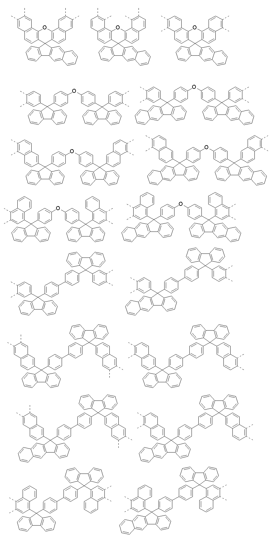
W1で表される4価の有機基は芳香環上に結合手を有し、結合手は芳香環の一辺に隣接して存在することが好ましく、その場合、フルオレンの9位の置換基とベンゾピラン型のヘテロ環構造を2組構成する。このような構造を取ることにより硬化性と伴に耐熱性とエッチング耐性が向上する。 The tetravalent organic group represented by W1 has a bond on the aromatic ring, and the bond is preferably present adjacent to one side of the aromatic ring. In that case, the substituent at the 9-position of fluorene and benzopyran It constitutes two sets of heterocyclic structures of the type. By adopting such a structure, not only curability but also heat resistance and etching resistance are improved.
上記一般式中(1)中のW2は炭素数1~50の2価の有機基であり、具体的には下記に示される構造などを例示することができる。

さらに本発明の重合体は、下記一般式(2)または(3)で示される繰り返し単位を有することが好ましい。


上記一般式(2)のAR5はベンゼン環、ナフタレン環を表し、下記を好ましい例として例示できる。この中でもナフタレン環がエッチング耐性の観点から好ましい。

上記一般式(3)中のAR6、AR7、W3で構成される4価の有機基の好ましい例として下記などを例示できる、この中でもナフタレン環、フルオレン構造を有するものが特に好ましく、ナフタレン環、フルオレン環構造を両方有するものが特に好ましい。

さらに本発明の重合体は、下記一般式(4)または(5)で示される繰り返し単位を有することが好ましい。
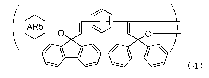

このようにW2で示される2価の有機基はベンゼン環であることが特に好ましく、AR1、AR2、AR3、AR4で構成される構造はフルオレンであることが原料入手の容易さから特に好ましい。 Thus, the divalent organic group represented by W2 is particularly preferably a benzene ring, and the structure composed of AR1, AR2, AR3, and AR4 is particularly preferably fluorene from the viewpoint of easy availability of raw materials.
さらに本発明の重合体の末端構造が下記一般式(6)または(7)のいずれかであることが好ましい。


![]()
![]()
上記一般式(6)としては下記などが例示できる。この中でも原料入手の容易さからAR8、AR9で構成される構造がフルオレン、かつ、R1が水素原子であることが特に好ましい。 Examples of the above general formula (6) include the following. Among these, it is particularly preferable that the structure composed of AR8 and AR9 is fluorene, and R1 is a hydrogen atom, in view of easy availability of raw materials.

AR8、AR9、R1の構造を要求性能に合わせて調整することが可能である。例えば、R1のアルキル鎖長を調整することで、重合体の溶剤溶解性、熱流動性、硬化性を制御することができる。また、AR8、AR9に耐熱性、エッチング耐性を向上させるためナフタレン環を導入、また、AR8,AR9をベンゼン環、ナフタレン環の組み合わせとすることで重合体の凝集性を低下させ溶剤溶解性を改善することなどができる。 It is possible to adjust the structures of AR8, AR9, and R1 to meet required performance. For example, by adjusting the alkyl chain length of R1, the solvent solubility, thermal fluidity, and curability of the polymer can be controlled. In addition, a naphthalene ring is introduced into AR8 and AR9 to improve heat resistance and etching resistance, and by combining AR8 and AR9 with a benzene ring and a naphthalene ring, the cohesiveness of the polymer is reduced and solvent solubility is improved. You can do things like that.
上記一般式(7)としては下記などが例示できる。この中でも原料入手の容易さからAR10、AR11で構成される構造がフルオレン、かつ、W4がベンゼン環、またはナフタレン環であることが特に好ましい。 Examples of the above general formula (7) include the following. Among these, it is particularly preferable that the structure composed of AR10 and AR11 is fluorene, and W4 is a benzene ring or a naphthalene ring, in view of easy availability of raw materials.


AR10、AR11、W4の構造はエッチング耐性、耐熱性、溶剤溶解性、熱流動性などの要求性能に合わせて調整することが可能であり、上記式(8)で示される熱硬化基として作用するR2の構造もベーク温度に合わせて適宜選択することが可能である。例えば、AR10、AR11がベンゼン環となった場合はフルオレン構造となり、原料の入手が容易となる。W4がベンゼン環、ナフタレン環となった場合も同様である。また、W4にフルオレン構造などの縮合芳香環構造を多く含む構造を導入することで耐熱性やエッチング耐性の向上も期待できる。また、R2の置換数を多くすることでベーク温度を下げることも可能となる。 The structures of AR10, AR11, and W4 can be adjusted to meet the required performance such as etching resistance, heat resistance, solvent solubility, and thermal fluidity, and act as a thermosetting group represented by the above formula (8). The structure of R2 can also be appropriately selected depending on the baking temperature. For example, when AR10 and AR11 are benzene rings, the structure becomes a fluorene structure, and the raw materials can be easily obtained. The same applies when W4 is a benzene ring or a naphthalene ring. Further, by introducing a structure containing a large amount of condensed aromatic ring structures such as a fluorene structure into W4, improvement in heat resistance and etching resistance can be expected. Furthermore, by increasing the number of R2 substitutions, it is also possible to lower the baking temperature.
さらに上記記載の重合体のMw(重量平均分子量)が500~5000であることが好ましく、さらにMwが600~4000であることが好ましい。なお、分子量は、テトラヒドロフランを溶離液としたゲルパーミエーションクロマトグラフィー(GPC)によるポリスチレン換算の重量平均分子量(Mw)として求めることができる。 Further, the Mw (weight average molecular weight) of the above-mentioned polymer is preferably 500 to 5,000, and more preferably 600 to 4,000. The molecular weight can be determined as a weight average molecular weight (Mw) in terms of polystyrene by gel permeation chromatography (GPC) using tetrahydrofuran as an eluent.
このような分子量であれば、有機溶剤への溶解性を確保でき、ベーク時に生じる昇華物を抑制することができる。また有機膜形成材料用重合体の熱流動性が良好なものとなるため、組成物に配合した際に、基板上に形成されている微細構造を良好に埋め込むことが可能になるだけでなく、基板全体が平坦となる有機膜を形成することができる。 With such a molecular weight, solubility in organic solvents can be ensured, and sublimation products generated during baking can be suppressed. In addition, since the polymer for organic film forming material has good thermal fluidity, when it is blended into a composition, it not only becomes possible to embed the fine structure formed on the substrate well, but also An organic film whose entire substrate is flat can be formed.
[重合体の製造方法]
本発明の一般式(1)で示される繰り返し単位を有する重合体の製造方法の一例として、下記に示されるW1を部分構造とするジオール化合物とAR1、AR2、AR3、AR4、W2から構成されるフルオレノール類をモノマーとして用いた、脱水を伴う環化反応を繰り返すことにより重合体を合成することができる。縮合によりベンゾピラン構造を形成するためジオールの水酸基はフェノール性水酸基を表し、ジオール化合物は具体的にはカテコール、レゾルシノールなどのベンゼンジオール類や1,5-ジヒドロキシナフタレン、2,6-ジヒドロキシナフタレンなどのナフタレンジオール類、ビスフェノールA、ビスヒドロキシフェニルフルオレンなどのビスフェノール類、ビスヒドロキシナフチルフルオレンなどのビスナフトール類を表す。下記式中のW1、AR1、AR2、AR3、AR4、W2は前記と同じ。
[Production method of polymer]
As an example of the method for producing a polymer having a repeating unit represented by the general formula (1) of the present invention, it is composed of a diol compound having W1 as a partial structure shown below and AR1, AR2, AR3, AR4, and W2. A polymer can be synthesized by repeating a cyclization reaction accompanied by dehydration using fluorenols as a monomer. In order to form a benzopyran structure through condensation, the hydroxyl group of the diol represents a phenolic hydroxyl group, and diol compounds include benzenediols such as catechol and resorcinol, and naphthalenes such as 1,5-dihydroxynaphthalene and 2,6-dihydroxynaphthalene. Represents diols, bisphenols such as bisphenol A and bishydroxyphenylfluorene, and bisnaphthols such as bishydroxynaphthylfluorene. W1, AR1, AR2, AR3, AR4, and W2 in the following formula are the same as above.

上記の重合体は、通常、有機溶媒中で酸触媒の存在下、室温または必要に応じて冷却または加熱下で得ることが出来る。用いられる酸触媒として、塩酸、臭化水素酸、硫酸、硝酸、リン酸、ヘテロポリ酸等の無機酸類、シュウ酸、トリフルオロ酢酸、メタンスルホン酸、ベンゼンスルホン酸、p-トルエンスルホン酸、トリフルオロメタンスルホン酸等の有機酸類、三塩化アルミニウム、アルミニウムエトキシド、アルミニウムイソプロポキシド、三フッ化ホウ素、三塩化ホウ素、三臭化ホウ素、四塩化錫、四臭化錫、二塩化ジブチル錫、ジブチル錫ジメトキシド、ジブチル錫オキシド、四塩化チタン、四臭化チタン、チタン(IV)メトキシド、チタン(IV)エトキシド、チタン(IV)イソプロポキシド、酸化チタン(IV)等のルイス酸類を用いることができる。 The above polymer can be obtained usually in an organic solvent in the presence of an acid catalyst at room temperature or under cooling or heating as required. Acid catalysts used include inorganic acids such as hydrochloric acid, hydrobromic acid, sulfuric acid, nitric acid, phosphoric acid, and heteropolyacids, oxalic acid, trifluoroacetic acid, methanesulfonic acid, benzenesulfonic acid, p-toluenesulfonic acid, and trifluoromethane. Organic acids such as sulfonic acid, aluminum trichloride, aluminum ethoxide, aluminum isopropoxide, boron trifluoride, boron trichloride, boron tribromide, tin tetrachloride, tin tetrabromide, dibutyltin dichloride, dibutyltin Lewis acids such as dimethoxide, dibutyltin oxide, titanium tetrachloride, titanium tetrabromide, titanium (IV) methoxide, titanium (IV) ethoxide, titanium (IV) isopropoxide, and titanium (IV) oxide can be used.
用いられる有機溶媒としては、特に制限はないが、メタノール、エタノール、イソプロピルアルコール、ブタノール、エチレングリコール、プロピレングリコール、ジエチレングリコール、グリセロール、エチレングリコールモノメチルエーテル、プロピレングリコールモノメチルエーテル等のアルコール類、ジエチルエーテル、ジブチルエーテル、ジエチレングリコールジエチルエーテル、ジエチレングリコールジメチルエーテル、テトラヒドロフラン、1,4-ジオキサン等のエーテル類、塩化メチレン、クロロホルム、ジクロロエタン、トリクロロエチレン等の塩素系溶剤類、ヘキサン、ヘプタン、ベンゼン、トルエン、キシレン、クメン等の炭化水素類、アセトニトリル等のニトリル類、アセトン、エチルメチルケトン、イソブチルメチルケトンなどのケトン類、酢酸エチル、酢酸n-ブチル、プロピレングリコールメチルエーテルアセテートなどのエステル類、ジメチルスルホキシド、N,N-ジメチルホルムアミド、ヘキサメチルホスホリックトリアミド等の非プロトン性極性溶媒類が例示でき、これらを単独あるいは2種類以上を混合して用いることができる。 The organic solvent used is not particularly limited, but alcohols such as methanol, ethanol, isopropyl alcohol, butanol, ethylene glycol, propylene glycol, diethylene glycol, glycerol, ethylene glycol monomethyl ether, propylene glycol monomethyl ether, diethyl ether, diethylene glycol, etc. Ethers such as butyl ether, diethylene glycol diethyl ether, diethylene glycol dimethyl ether, tetrahydrofuran, 1,4-dioxane, chlorinated solvents such as methylene chloride, chloroform, dichloroethane, trichloroethylene, carbonization of hexane, heptane, benzene, toluene, xylene, cumene, etc. Hydrogens, nitriles such as acetonitrile, ketones such as acetone, ethyl methyl ketone, isobutyl methyl ketone, esters such as ethyl acetate, n-butyl acetate, propylene glycol methyl ether acetate, dimethyl sulfoxide, N,N-dimethylformamide Examples include aprotic polar solvents such as , hexamethylphosphoric triamide, etc., and these can be used alone or in combination of two or more.
反応方法としては、ジオール化合物、フルオレノール類と触媒である酸触媒を一括で仕込む方法、ジオール化合物、フルオレノール類を分散または溶解後、触媒を一括または分割により添加する方法や溶剤で希釈し滴下する方法、触媒を分散後または溶解後、フルオレノール類またはジオール化合物を一括または分割により添加する方法や、溶剤で希釈し滴下する方法がある。反応終了後、反応に使用した触媒を除去するために有機溶剤に希釈後、分液洗浄を行い目的物を回収できる。 Reaction methods include adding the diol compound, fluorenol and the acid catalyst all at once, dispersing or dissolving the diol compound and fluorenol, then adding the catalyst all at once or in portions, or diluting with a solvent and adding it dropwise. After dispersing or dissolving the catalyst, there is a method in which fluorenols or diol compounds are added all at once or in portions, and a method in which the catalyst is diluted with a solvent and added dropwise. After the reaction is completed, the target product can be recovered by diluting it with an organic solvent to remove the catalyst used in the reaction and then performing liquid separation washing.
この時使用する有機溶剤としては、目的物を溶解でき、水と混合しても2層分離するものであれば特に制限はないが、例えばヘキサン、ヘプタン、ベンゼン、トルエン、キシレン等の炭化水素類、酢酸エチル、酢酸n-ブチル、プロピレングリコールメチルエーテルアセテート等のエステル類、メチルエチルケトン、メチルアミルケトン、シクロヘキサノン、メチルイソブチルケトン等のケトン類、ジエチルエーテル、ジイソプロピルエーテル、メチル-t-ブチルエーテル、エチルシクロペンチルメチルエーテル等のエーテル類、塩化メチレン、クロロホルム、ジクロロエタン、トリクロロエチレン等の塩素系溶剤類、及びこれらの混合物などを挙げることが出来る。この際に使用する洗浄水は、通常、脱イオン水や超純水と呼ばれているものを使用すればよい。洗浄回数は1回以上あればよいが、10回以上洗浄しても洗浄しただけの効果は得られるとは限らないため、好ましくは1~5回程度である。 The organic solvent used at this time is not particularly limited as long as it can dissolve the target substance and separate into two layers even when mixed with water, but examples include hydrocarbons such as hexane, heptane, benzene, toluene, and xylene. , esters such as ethyl acetate, n-butyl acetate, propylene glycol methyl ether acetate, ketones such as methyl ethyl ketone, methyl amyl ketone, cyclohexanone, methyl isobutyl ketone, diethyl ether, diisopropyl ether, methyl t-butyl ether, ethyl cyclopentyl methyl Examples include ethers such as ether, chlorinated solvents such as methylene chloride, chloroform, dichloroethane, trichloroethylene, and mixtures thereof. The cleaning water used at this time may be generally deionized water or ultrapure water. The number of times of washing may be one or more times, but it is preferably about 1 to 5 times since washing 10 times or more does not necessarily provide the same effect as washing alone.
分液洗浄の際に系内の酸性成分を除去するため、塩基性水溶液で洗浄を行ってもよい。塩基としては、具体的には、アルカリ金属の水酸化物、アルカリ金属の炭酸塩、アルカリ土類金属の水酸化物、アルカリ土類金属の炭酸塩、アンモニア、及び有機アンモニウム等が挙げられる。 In order to remove acidic components in the system during liquid separation washing, washing may be performed with a basic aqueous solution. Specific examples of the base include alkali metal hydroxides, alkali metal carbonates, alkaline earth metal hydroxides, alkaline earth metal carbonates, ammonia, and organic ammonium.
更に、分液洗浄の際に系内の金属不純物または塩基成分を除去するため、酸性水溶液で洗浄を行ってもよい。酸としては、具体的には、塩酸、臭化水素酸、硫酸、硝酸、リン酸、ヘテロポリ酸等の無機酸類、シュウ酸、フマル酸、マレイン酸、トリフルオロ酢酸、メタンスルホン酸、ベンゼンスルホン酸、p-トルエンスルホン酸、トリフルオロメタンスルホン酸等の有機酸類等が挙げられる。 Furthermore, in order to remove metal impurities or basic components in the system during liquid separation cleaning, cleaning may be performed with an acidic aqueous solution. Examples of acids include inorganic acids such as hydrochloric acid, hydrobromic acid, sulfuric acid, nitric acid, phosphoric acid, and heteropolyacids, oxalic acid, fumaric acid, maleic acid, trifluoroacetic acid, methanesulfonic acid, and benzenesulfonic acid. , p-toluenesulfonic acid, trifluoromethanesulfonic acid, and other organic acids.
上記の塩基性水溶液、酸性水溶液による分液洗浄はいずれか一方のみでもよいが、組み合わせて行うこともできる。分液洗浄は、塩基性水溶液、酸性水溶液の順に行うのが金属不純物除去の観点から好ましい。 The above-mentioned separation washing using a basic aqueous solution or an acidic aqueous solution may be carried out using only one of them, but they can also be carried out in combination. From the viewpoint of removing metal impurities, it is preferable to perform liquid separation washing in the order of a basic aqueous solution and an acidic aqueous solution.
上記の塩基性水溶液、酸性水溶液による分液洗浄後、続けて中性の水で洗浄してもよい。洗浄回数は1回以上行えばよいが、好ましくは1~5回程度である。中性水としては、上記で述べた脱イオン水や超純水等を使用すればよい。洗浄回数は1回以上であればよいが、回数が少なくては塩基成分、酸性成分を除去できないことがある。10回以上洗浄しても洗浄しただけの効果は得られるとは限らないため、好ましくは1~5回程度である。 After the liquid separation washing with the above basic aqueous solution and acidic aqueous solution, washing with neutral water may be continued. The number of washings may be one or more times, but preferably about 1 to 5 times. As the neutral water, the above-mentioned deionized water, ultrapure water, etc. may be used. The number of washings may be one or more times, but if the number of washings is too small, the basic components and acidic components may not be removed. Even if it is washed 10 times or more, the effect of washing alone will not necessarily be obtained, so it is preferably about 1 to 5 times.
更に、分液操作後の反応生成物は減圧又は常圧で溶剤を濃縮乾固又は晶出操作を行い粉体として回収することもできるが、有機膜形成材料を調製する際の操作性改善のため、適度な濃度の溶液状態にしておくことも可能である。このときの濃度としては、0.1~50質量%が好ましく、より好ましくは0.5~30重量%である。このような濃度であれば、粘度が高くなりにくいことから操作性を損なうことを防止することができ、また、溶剤の量が過大となることがないことから経済的になる。 Furthermore, the reaction product after the liquid separation operation can be recovered as a powder by concentrating the solvent to dryness or crystallizing it under reduced pressure or normal pressure. Therefore, it is also possible to keep it in a solution state with an appropriate concentration. The concentration at this time is preferably 0.1 to 50% by weight, more preferably 0.5 to 30% by weight. With such a concentration, the viscosity does not easily increase, so it is possible to prevent the operability from being impaired, and it is also economical because the amount of solvent does not become excessive.
このときの溶剤としては、重合体を溶解できるものであれば特に制限はないが、具体例を挙げると、シクロヘキサノン、メチル-2-アミルケトン等のケトン類;3-メトキシブタノール、3-メチル-3-メトキシブタノール、1-メトキシ-2-プロパノール、1-エトキシ-2-プロパノール等のアルコール類、プロピレングリコールモノメチルエーテル、エチレングリコールモノメチルエーテル、プロピレングリコールモノエチルエーテル、エチレングリコールモノエチルエーテル、プロピレングリコールジメチルエーテル、ジエチレングリコールジメチルエーテル等のエーテル類;プロピレングリコールモノメチルエーテルアセテート、プロピレングリコールモノエチルエーテルアセテート、乳酸エチル、ピルビン酸エチル、酢酸ブチル、3-メトキシプロピオン酸メチル、3-エトキシプロピオン酸エチル、酢酸tert-ブチル、プロピオン酸tert-ブチル、プロピレングリコールモノtert-ブチルエーテルアセテート等のエステル類が挙げられ、これらを単独あるいは2種類以上を混合して用いることができる。 The solvent at this time is not particularly limited as long as it can dissolve the polymer, but specific examples include ketones such as cyclohexanone and methyl-2-amyl ketone; 3-methoxybutanol, 3-methyl-3 -Alcohols such as methoxybutanol, 1-methoxy-2-propanol, 1-ethoxy-2-propanol, propylene glycol monomethyl ether, ethylene glycol monomethyl ether, propylene glycol monoethyl ether, ethylene glycol monoethyl ether, propylene glycol dimethyl ether, Ethers such as diethylene glycol dimethyl ether; propylene glycol monomethyl ether acetate, propylene glycol monoethyl ether acetate, ethyl lactate, ethyl pyruvate, butyl acetate, methyl 3-methoxypropionate, ethyl 3-ethoxypropionate, tert-butyl acetate, propion Examples include esters such as tert-butyl acid and propylene glycol mono-tert-butyl ether acetate, and these can be used alone or in combination of two or more.
本発明の一般式(6)で示される末端構造を有する重合体としては、例えば、下記の通り、上記のジオール化合物とフルオレノール類の仕込み比率をフルオレノール類を過剰にして反応後、さらに末端を水またはR1-OHで表されるアルコールにより封止することにより得ることができる。下記式中のAR1、AR2、AR3、AR4、AR8、AR9、W1、W2、R1は上記と同じである。 The polymer having the terminal structure represented by the general formula (6) of the present invention can be prepared, for example, by changing the charging ratio of the diol compound and fluorenol to an excess of the fluorenol as shown below, and then reacting the terminal with water. Alternatively, it can be obtained by sealing with an alcohol represented by R1-OH. AR1, AR2, AR3, AR4, AR8, AR9, W1, W2, and R1 in the following formula are the same as above.

本発明の一般式(7)で示される末端構造を有する重合体としては、例えば、下記の通り、上記ジオール化合物とフルオレノール類の仕込み比率をフルオレノール類を過剰にして反応後、W4を部分構造としてもつアルコール類で封止することにより得ることができる。下記式中のAR1、AR2、AR3、AR4、AR10、AR11、W1、W2、W4、R2、nは前記と同じである。 The polymer having the terminal structure represented by the general formula (7) of the present invention can be prepared, for example, as shown below, by changing the charging ratio of the diol compound and fluorenols to an excess of fluorenol, and then reacting with W4 as a partial structure. It can be obtained by sealing with alcohols. AR1, AR2, AR3, AR4, AR10, AR11, W1, W2, W4, R2, and n in the following formula are the same as above.

上記の重合体の反応方法、回収方法は上記の重合体の製造方法のうち一般式(1)で示される繰り返し単位を有する重合体を合成する方法の箇所で記載した方法で反応、回収することができる。 The reaction and recovery method for the above polymer is as described in the method for synthesizing a polymer having a repeating unit represented by general formula (1) among the above polymer production methods. I can do it.
また、本発明の有機膜形成材料に用いられる重合体のうち一般式(7)で表される末端構造基のうちR2がプロパルギルエーテルの場合、下記のとおり、1段階目に上記ジオール化合物とフルオレノール類の仕込み比率をジオール化合物を過剰にして反応を行い末端にアルコールが残存した重合体を合成後、さらに2段階目として残存したアルコールをプロパルギルエーテル化する方法などが例示できる。プロパルギルエーテル基を導入できる反応であれば特に限定は無いが、下記のようなプロパルギル基を有するハロゲン化物またはトシレート、メシレートと塩基触媒を用いた置換反応等が例示できる。下記式中のXはハロゲン、トシル基またはメシル基を表す、下記式中のAR1、AR2、AR3、AR4、AR10、AR11、W1、W2、W4は前記と同じである。 In addition, when R2 of the terminal structural group represented by general formula (7) in the polymer used in the organic film-forming material of the present invention is propargyl ether, the above diol compound and fluorenol are added in the first step as described below. Examples include a method in which the reaction is carried out using an excess of the diol compound to synthesize a polymer in which alcohol remains at the terminal, and then the remaining alcohol is converted into propargyl ether in a second step. There is no particular limitation as long as the reaction can introduce a propargyl ether group, but the following substitution reaction using a halide, tosylate, or mesylate and a base catalyst having a propargyl group can be exemplified. In the following formula, X represents a halogen, tosyl group or mesyl group, and AR1, AR2, AR3, AR4, AR10, AR11, W1, W2, and W4 in the following formula are the same as above.


置換反応に用いられる塩基触媒としては炭酸水素ナトリウム、炭酸ナトリウム、炭酸カリウム、炭酸カルシウム、炭酸セシウム、水酸化ナトリウム、水酸化カリウム、水素化ナトリウム、リン酸カリウム等の無機塩基化合物、トリエチルアミン、ピリジン、N-メチルモルホリン等の有機アミン化合等が挙げられ、これらを単独でも2種以上を組み合わせて用いてもよい。 Base catalysts used in the substitution reaction include inorganic base compounds such as sodium hydrogen carbonate, sodium carbonate, potassium carbonate, calcium carbonate, cesium carbonate, sodium hydroxide, potassium hydroxide, sodium hydride, potassium phosphate, triethylamine, pyridine, Examples include organic amine compounds such as N-methylmorpholine, and these may be used alone or in combination of two or more.
このときに用いられる溶媒としては、上記反応に不活性な溶剤であれば特に制限はないが、例えば、ジエチルエーテル、テトラヒドロフラン、ジオキサン等のエーテル系溶媒、ベンゼン、トルエン、キシレン等の芳香族系溶媒、アセトニトリル、ジメチルスルホキシド、N,N-ジメチルホルムアミド、N-メチルピロリドン、水等、これらを単独または混合して用いることができる。 The solvent used at this time is not particularly limited as long as it is inert to the above reaction, but examples include ether solvents such as diethyl ether, tetrahydrofuran, and dioxane, and aromatic solvents such as benzene, toluene, and xylene. , acetonitrile, dimethyl sulfoxide, N,N-dimethylformamide, N-methylpyrrolidone, water, etc. These can be used alone or in combination.
反応方法および重合体の回収方法については上記の重合体の製造方法のうち一般式(1)で示される繰り返し単位を有する重合体を合成する方法の箇所で記載した方法によって回収することができる。 Regarding the reaction method and the method for recovering the polymer, it can be recovered by the method described in the section of the method for synthesizing a polymer having a repeating unit represented by general formula (1) among the above-mentioned methods for producing a polymer.
この方法で得られる有機膜形成材料に用いられる重合体の調製には種々のハロゲン化物やトシレートおよびメシレートを要求性能に合わせて単独または複数組み合わせて用いることが可能である。例えば平坦化特性の向上に寄与する側鎖構造、エッチング耐性、耐熱性に寄与する剛直な芳香環構造などを持つものを任意の割合で組み合わせることができる。そのためこれらの重合体を用いた有機膜形成材料は埋め込み/平坦化特性とエッチング耐性を高い次元で両立することが可能となる。 In preparing the polymer used in the organic film-forming material obtained by this method, various halides, tosylates, and mesylates can be used singly or in combination depending on the required performance. For example, materials having a side chain structure that contributes to improving planarization properties, a rigid aromatic ring structure that contributes to etching resistance, heat resistance, etc. can be combined in any proportion. Therefore, organic film forming materials using these polymers can achieve both high levels of embedding/planarization characteristics and etching resistance.
以上のように、本発明の有機膜形成材料用重合体であれば、高いエッチング耐性、優れたよれ耐性を発現できる有機膜形成材料を与えるものとなる。 As described above, the polymer for organic film-forming materials of the present invention provides an organic film-forming material that can exhibit high etching resistance and excellent kink resistance.
<有機膜形成材料>
また、本発明では、有機膜形成用の材料であって、(A)上述の本発明の有機膜形成材料用重合体及び(B)有機溶剤を含有する有機膜形成材料を提供する。なお、本発明の有機膜形成材料において、本発明の有機膜形成材料用重合体を単独又は複数組み合わせて用いることができる。
<Organic film forming material>
The present invention also provides an organic film-forming material containing (A) the above-described polymer for organic film-forming materials of the present invention and (B) an organic solvent. In addition, in the organic film-forming material of the present invention, the polymer for organic film-forming material of the present invention can be used alone or in combination.
[(B)有機溶剤]
本発明の有機膜形成材料において使用可能な有機溶剤としては、上記の重合体(ベースポリマー)、及び含まれる場合には後述の酸発生剤、架橋剤、その他添加剤等が溶解するものであれば特に制限はない。具体的には、特開2007-199653号公報中の[0091]~[0092]段落に記載されている溶剤などの沸点が180℃未満の溶剤を使用することができる。中でも、プロピレングリコールモノメチルエーテルアセテート、プロピレングリコールモノメチルエーテル、2-ヘプタノン、シクロペンタノン、シクロヘキサノン及びこれらのうち2種以上の混合物が好ましく用いられる。有機溶剤の配合量は、(A)前記重合体100部に対して好ましくは200~10,000部、より好ましくは300~5,000部である。
[(B) Organic solvent]
Examples of organic solvents that can be used in the organic film-forming material of the present invention include those that can dissolve the above polymer (base polymer) and, if included, the acid generator, crosslinking agent, and other additives described below. There are no particular restrictions. Specifically, a solvent having a boiling point of less than 180° C. can be used, such as the solvents described in paragraphs [0091] to [0092] of JP-A-2007-199653. Among them, propylene glycol monomethyl ether acetate, propylene glycol monomethyl ether, 2-heptanone, cyclopentanone, cyclohexanone, and mixtures of two or more of these are preferably used. The amount of the organic solvent to be blended is preferably 200 to 10,000 parts, more preferably 300 to 5,000 parts, based on 100 parts of the polymer (A).
このような有機膜形成材料であれば、回転塗布で塗布することができ、また上述のような本発明の有機膜形成材料用重合体を含有するため、良好なドライエッチング耐性を有するとともに耐熱性及び高度な埋め込み/平坦化特性を併せ持つ有機膜形成材料となる。 Such an organic film-forming material can be applied by spin coating, and since it contains the above-mentioned polymer for organic film-forming materials of the present invention, it has good dry etching resistance and heat resistance. It is an organic film forming material that also has advanced embedding/planarization properties.
さらに、本発明の有機膜形成材料には有機溶剤として、上記の沸点が180℃未満の溶剤に沸点が180℃以上の高沸点溶剤を添加する事も可能である(沸点が180℃未満の溶剤と沸点が180℃以上の溶剤の混合物)。高沸点有機溶剤としては、有機膜形成材料用重合体を溶解できるものであれば、炭化水素類、アルコール類、ケトン類、エステル類、エーテル類、塩素系溶剤等の制限は特にはないが、具体例として1-オクタノール、2-エチルヘキサノール、1-ノナノール、1-デカノール、1-ウンデカノール、エチレングリコール、1,2-プロピレングリコール、1,3-ブチレングリコール、2,4-ペンタンジオール、2-メチル-2,4-ペンタンジオール、2,5-ヘキサンジオール、2,4-ヘプタンジオール、2-エチル-1,3-ヘキサンジオール、ジエチレングリコール、ジプロピレングリコール、トリエチレングリコール、トリプロピレングリコール、グリセリン、酢酸n-ノニル、エチレングリコールモノヘキシルエーテル、エチレングリコールモノー2-エチルヘキシルエーテル、エチレングリコールモノフェニルエーテル、エチレングリコールモノベンジルエーテル、ジエチレングリコールモノエチルエーテル、ジエチレングリコールモノイソプロピルエーテル、ジエチレングリコールモノ-n-ブチルエーテル、ジエチレングリコールモノイソブチルエーテル、ジエチレングリコールモノヘキシルエーテル、ジエチレングリコールモノフェニルエーテル、ジエチレングリコールモノベンジルエーテル、ジエチレングリコールジエチルエーテル、ジエチレングリコールジブチルエーテル、ジエチレングリコールブチルメチルエーテル、トリエチレングリコールジメチルエーテル、トリエチレングリコールモノメチルエーテル、トリエチレングリコール-n-ブチルエーテル、トリエチレングリコールブチルメチルエーテル、トリエチレングリコールジアセテート、テトラエチレングリコールジメチルエーテル、ジプロピレングリコールモノメチルエーテル、ジプロピレングリコールモノ-n-プロピルエーテル、ジプロピレングリコールモノ-n-ブチルエーテル、トリプロピレングリコールジメチルエーテル、トリプロピレングリコールモノメチルエーテル、トリプロピレングリコールモノ-n-プロピルエーテル、トリプロピレングリコールモノ-n-ブチルエーテル、エチレングリコールモノエチルエーテルアセテート、エチレングリコールモノブチルエーテルアセテート、ジエチレングリコールモノメチルエーテルアセテート、ジエチレングリコールモノエチルエーテルアセテート、ジエチレングリコールモノブチルエーテルアセテート、トリアセチン、プロピレングリコールジアセテート、ジプロピレングリコールモノメチルエーテルアセテート、ジプロピレングリコールメチル-n-プロピルエーテル、ジプロピレングリコールメチルエーテルアセテート、1,4―ブタンジオールジアセテート、1,3―ブチレングリコールジアセテート、1,6-ヘキサンジオールジアセテート、トリエチレングリコールジアセテート、γ-ブチロラクトン、マロン酸ジヘキシル、コハク酸ジエチル、コハク酸ジプロピル、コハク酸ジブチル、コハク酸ジヘキシル、アジピン酸ジメチル、アジピン酸ジエチル、アジピン酸ジブチルなどを例示することができ、これらを単独または混合し用いても良い。 Furthermore, it is also possible to add a high boiling point solvent with a boiling point of 180°C or more to the above-mentioned solvent with a boiling point of less than 180°C as an organic solvent to the organic film-forming material of the present invention. and a solvent with a boiling point of 180°C or higher). There are no particular restrictions on the high boiling point organic solvent, as long as it can dissolve the polymer for organic film forming materials, such as hydrocarbons, alcohols, ketones, esters, ethers, chlorinated solvents, etc. Specific examples include 1-octanol, 2-ethylhexanol, 1-nonanol, 1-decanol, 1-undecanol, ethylene glycol, 1,2-propylene glycol, 1,3-butylene glycol, 2,4-pentanediol, 2- Methyl-2,4-pentanediol, 2,5-hexanediol, 2,4-heptanediol, 2-ethyl-1,3-hexanediol, diethylene glycol, dipropylene glycol, triethylene glycol, tripropylene glycol, glycerin, n-nonyl acetate, ethylene glycol monohexyl ether, ethylene glycol mono-2-ethylhexyl ether, ethylene glycol monophenyl ether, ethylene glycol monobenzyl ether, diethylene glycol monoethyl ether, diethylene glycol monoisopropyl ether, diethylene glycol mono-n-butyl ether, diethylene glycol mono Isobutyl ether, diethylene glycol monohexyl ether, diethylene glycol monophenyl ether, diethylene glycol monobenzyl ether, diethylene glycol diethyl ether, diethylene glycol dibutyl ether, diethylene glycol butyl methyl ether, triethylene glycol dimethyl ether, triethylene glycol monomethyl ether, triethylene glycol-n-butyl ether, Triethylene glycol butyl methyl ether, triethylene glycol diacetate, tetraethylene glycol dimethyl ether, dipropylene glycol monomethyl ether, dipropylene glycol mono-n-propyl ether, dipropylene glycol mono-n-butyl ether, tripropylene glycol dimethyl ether, tripropylene Glycol monomethyl ether, tripropylene glycol mono-n-propyl ether, tripropylene glycol mono-n-butyl ether, ethylene glycol monoethyl ether acetate, ethylene glycol monobutyl ether acetate, diethylene glycol monomethyl ether acetate, diethylene glycol monoethyl ether acetate, diethylene glycol monobutyl ether Acetate, triacetin, propylene glycol diacetate, dipropylene glycol monomethyl ether acetate, dipropylene glycol methyl-n-propyl ether, dipropylene glycol methyl ether acetate, 1,4-butanediol diacetate, 1,3-butylene glycol diacetate , 1,6-hexanediol diacetate, triethylene glycol diacetate, γ-butyrolactone, dihexyl malonate, diethyl succinate, dipropyl succinate, dibutyl succinate, dihexyl succinate, dimethyl adipate, diethyl adipate, adipic acid Examples include dibutyl, which may be used alone or in combination.
上記、高沸点溶剤の沸点は、有機膜形成材料を熱処理する温度に合わせて適宜選択すればよく、添加する高沸点溶剤の沸点は180℃~300℃であることが好ましく、200℃~300℃であることがより好ましい。このような沸点であれば沸点が低すぎることによってベーク(熱処理)した際の揮発が速すぎる恐れがないため、十分な熱流動性を得ることができる。また、このような沸点であれば沸点が高すぎることなくベーク後も膜中に揮発せずに残存してしまうことがないため、エッチング耐性等の膜物性に悪影響を及ぼす恐れがない。 The boiling point of the above-mentioned high boiling point solvent may be appropriately selected according to the temperature at which the organic film forming material is heat treated, and the boiling point of the high boiling point solvent to be added is preferably 180°C to 300°C, and preferably 200°C to 300°C. It is more preferable that With such a boiling point, sufficient thermal fluidity can be obtained because there is no risk that the boiling point will be too low and volatilization will be too rapid during baking (heat treatment). In addition, if the boiling point is such, the boiling point will not be too high and will not remain in the film without being volatilized even after baking, so there is no risk of adversely affecting the physical properties of the film such as etching resistance.
また、上記、高沸点溶剤を使用する場合、高沸点溶剤の配合量は、沸点180℃未満の溶剤100質量部に対して1~30質量部とすることが好ましい。このような配合量であれば、配合量が少なすぎてベーク時に十分な熱流動性が付与することができなくなったり、配合量が多すぎて膜中に残存しエッチング耐性などの膜物性の劣化につながったりする恐れがない。 Further, when the above-mentioned high boiling point solvent is used, the amount of the high boiling point solvent blended is preferably 1 to 30 parts by mass per 100 parts by mass of the solvent having a boiling point of less than 180°C. If this amount is used, the amount may be too small to provide sufficient thermal fluidity during baking, or the amount may be too large and may remain in the film, resulting in deterioration of film properties such as etching resistance. There is no fear that it will lead to
このような有機膜形成材料であれば、上記の有機膜形成材料に高沸点溶剤の添加による熱流動性が付与されることで、高度な埋め込み/平坦化特性を併せ持つ有機膜形成用組成物となる。 Such an organic film-forming material can be made into an organic film-forming composition that has advanced embedding/flattening properties by imparting thermal fluidity to the above-mentioned organic film-forming material by adding a high boiling point solvent. Become.
[(C)酸発生剤]
本発明の有機膜形成材料においては、硬化反応を更に促進させるために(C)酸発生剤を添加することができる。酸発生剤は熱分解によって酸を発生するものや、光照射によって酸を発生するものがあるが、いずれのものも添加することができる。具体的には、特開2007-199653号公報中の[0061]~[0085]段落に記載されている材料を添加することができるがこれらに限定されない。
[(C) Acid generator]
In the organic film-forming material of the present invention, an acid generator (C) can be added to further promote the curing reaction. There are acid generators that generate acid through thermal decomposition and those that generate acid through light irradiation, and any of these can be added. Specifically, materials described in paragraphs [0061] to [0085] of JP-A No. 2007-199653 can be added, but are not limited thereto.
上記酸発生剤は1種を単独で又は2種以上を組み合わせて用いることができる。酸発生剤を添加する場合の添加量は、(A)前記重合体100部に対して好ましくは0.05~50部、より好ましくは0.1~10部である。 The above acid generators can be used alone or in combination of two or more. When adding an acid generator, the amount added is preferably 0.05 to 50 parts, more preferably 0.1 to 10 parts, based on 100 parts of the polymer (A).
[(D)界面活性剤]
本発明の有機膜形成材料には、スピンコーティングにおける塗布性を向上させるために(D)界面活性剤を添加することができる。界面活性剤としては、例えば、特開2009-269953号公報中の[0142]~[0147]記載のものを用いることができる。界面活性剤を添加する場合の添加量は、(A)前記重合体100部に対して好ましくは0.01~10部、より好ましくは0.05~5部である。
[(D) Surfactant]
(D) a surfactant can be added to the organic film-forming material of the present invention in order to improve coating properties in spin coating. As the surfactant, for example, those described in [0142] to [0147] in JP-A No. 2009-269953 can be used. When adding a surfactant, the amount added is preferably 0.01 to 10 parts, more preferably 0.05 to 5 parts, based on 100 parts of the polymer (A).
[(E)架橋剤]
また、本発明の有機膜形成材料には、硬化性を高め、上層膜とのインターミキシングを更に抑制するために、(E)架橋剤を添加することもできる。架橋剤としては、特に限定されることはなく、公知の種々の系統の架橋剤を広く用いることができる。一例として、メラミン系架橋剤、グリコールウリル系架橋剤、ベンゾグアナミン系架橋剤、ウレア系架橋剤、β-ヒドロキシアルキルアミド系架橋剤、イソシアヌレート系架橋剤、アジリジン系架橋剤、オキサゾリン系架橋剤、エポキシ系架橋剤を例示できる。
[(E) Crosslinking agent]
Moreover, (E) a crosslinking agent can also be added to the organic film-forming material of the present invention in order to enhance curability and further suppress intermixing with the upper layer film. The crosslinking agent is not particularly limited, and a wide variety of known crosslinking agents can be used. Examples include melamine crosslinking agents, glycoluril crosslinking agents, benzoguanamine crosslinking agents, urea crosslinking agents, β-hydroxyalkylamide crosslinking agents, isocyanurate crosslinking agents, aziridine crosslinking agents, oxazoline crosslinking agents, and epoxy Examples include crosslinking agents.
メラミン系架橋剤として、具体的には、ヘキサメトキシメチル化メラミン、ヘキサブトキシメチル化メラミン、これらのアルコキシ及び/又はヒドロキシ置換体、及びこれらの部分自己縮合体を例示できる。グリコールウリル系架橋剤として、具体的には、テトラメトキシメチル化グリコールウリル、テトラブトキシメチル化グリコールウリル、これらのアルコキシ及び/又はヒドロキシ置換体、及びこれらの部分自己縮合体を例示できる。ベンゾグアナミン系架橋剤として、具体的には、テトラメトキシメチル化ベンゾグアナミン、テトラブトキシメチル化ベンゾグアナミン、これらのアルコキシ及び/又はヒドロキシ置換体、及びこれらの部分自己縮合体を例示できる。ウレア系架橋剤として、具体的には、ジメトキシメチル化ジメトキシエチレンウレア、このアルコキシ及び/又はヒドロキシ置換体、及びこれらの部分自己縮合体を例示できる。β-ヒドロキシアルキルアミド系架橋剤として具体的には、N,N,N’,N’-テトラ(2-ヒドロキシエチル)アジピン酸アミドを例示できる。イソシアヌレート系架橋剤として具体的には、トリグリシジルイソシアヌレート、トリアリルイソシアヌレートを例示できる。アジリジン系架橋剤として具体的には、4,4’-ビス(エチレンイミノカルボニルアミノ)ジフェニルメタン、2,2-ビスヒドロキシメチルブタノール-トリス[3-(1-アジリジニル)プロピオナート]を例示できる。オキサゾリン系架橋剤として具体的には、2,2’-イソプロピリデンビス(4-ベンジル-2-オキサゾリン)、2,2’-イソプロピリデンビス(4-フェニル-2-オキサゾリン)、2,2’-メチレンビス4,5-ジフェニル-2-オキサゾリン、2,2’-メチレンビス-4-フェニル-2-オキサゾリン、2,2’-メチレンビス-4-tertブチル-2-オキサゾリン、2,2’-ビス(2-オキサゾリン)、1,3-フェニレンビス(2-オキサゾリン)、1,4-フェニレンビス(2-オキサゾリン)、2-イソプロペニルオキサゾリン共重合体を例示できる。エポキシ系架橋剤として具体的には、ジグリシジルエーテル、エチレングリコールジグリシジルエーテル、1,4-ブタンジオールジグリシジルエーテル、1,4-シクロヘキサンジメタノールジグリシジルエーテル、ポリ(メタクリル酸グリシジル)、トリメチロールエタントリグリシジルエーテル、トリメチロールプロパントリグリシジルエーテル、ペンタエリスリトールテトラグリシジルエーテルを例示できる。架橋剤を添加する場合の添加量は、(A)前記重合体100部に対して好ましくは1~100部、より好ましくは5~50部である。 Specific examples of the melamine crosslinking agent include hexamethoxymethylated melamine, hexabutoxymethylated melamine, alkoxy and/or hydroxy substituted products thereof, and partial self-condensates thereof. Specific examples of the glycoluril crosslinking agent include tetramethoxymethylated glycoluril, tetrabutoxymethylated glycoluril, alkoxy- and/or hydroxy-substituted products thereof, and partial self-condensates thereof. Specific examples of the benzoguanamine crosslinking agent include tetramethoxymethylated benzoguanamine, tetrabutoxymethylated benzoguanamine, alkoxy and/or hydroxy substituted products thereof, and partially self-condensed products thereof. Specific examples of the urea-based crosslinking agent include dimethoxymethylated dimethoxyethylene urea, alkoxy- and/or hydroxy-substituted products thereof, and partial self-condensates thereof. A specific example of the β-hydroxyalkylamide crosslinking agent is N,N,N',N'-tetra(2-hydroxyethyl)adipamide. Specific examples of the isocyanurate-based crosslinking agent include triglycidyl isocyanurate and triallyl isocyanurate. Specific examples of the aziridine crosslinking agent include 4,4'-bis(ethyleneiminocarbonylamino)diphenylmethane and 2,2-bishydroxymethylbutanol-tris[3-(1-aziridinyl)propionate]. Specifically, the oxazoline crosslinking agents include 2,2'-isopropylidene bis(4-benzyl-2-oxazoline), 2,2'-isopropylidene bis(4-phenyl-2-oxazoline), 2,2' -Methylenebis4,5-diphenyl-2-oxazoline, 2,2'-methylenebis-4-phenyl-2-oxazoline, 2,2'-methylenebis-4-tertbutyl-2-oxazoline, 2,2'-bis( 2-oxazoline), 1,3-phenylenebis(2-oxazoline), 1,4-phenylenebis(2-oxazoline), and 2-isopropenyloxazoline copolymers. Specifically, the epoxy crosslinking agents include diglycidyl ether, ethylene glycol diglycidyl ether, 1,4-butanediol diglycidyl ether, 1,4-cyclohexanedimethanol diglycidyl ether, poly(glycidyl methacrylate), and trimethylol. Examples include ethane triglycidyl ether, trimethylolpropane triglycidyl ether, and pentaerythritol tetraglycidyl ether. When adding a crosslinking agent, the amount added is preferably 1 to 100 parts, more preferably 5 to 50 parts, based on 100 parts of the polymer (A).
[(F)可塑剤]
また、本発明の有機膜形成材料には、平坦化/埋め込み特性を更に向上させるために、(F)可塑剤を添加することができる。可塑剤としては、特に限定されることはなく、公知の種々の系統の可塑剤を広く用いることができる。一例として、フタル酸エステル類、アジピン酸エステル類、リン酸エステル類、トリメリット酸エステル類、クエン酸エステル類などの低分子化合物、ポリエーテル系、ポリエステル系、特開2013-253227記載のポリアセタール系重合体などのポリマーを例示できる。可塑剤を添加する場合の添加量は、(A)前記重合体100部に対して好ましくは1~100部、より好ましくは5~30部である。
[(F) Plasticizer]
Moreover, (F) a plasticizer can be added to the organic film forming material of the present invention in order to further improve the flattening/embedding characteristics. The plasticizer is not particularly limited, and a wide variety of known plasticizers can be used. Examples include low molecular weight compounds such as phthalate esters, adipate esters, phosphate esters, trimellitate esters, citric acid esters, polyethers, polyesters, and polyacetals as described in JP-A No. 2013-253227. Examples include polymers such as polymers. When adding a plasticizer, the amount added is preferably 1 to 100 parts, more preferably 5 to 30 parts, based on 100 parts of the polymer (A).
また、本発明の有機膜形成材料には、埋め込み/平坦化特性を可塑剤と同じように付与するための添加剤として、例えば、ポリエチレングリコール、ポリプロピレングリコール構造を有する液状添加剤、又は30℃から250℃までの間の重量減少率が40質量%以上であり、かつ重量平均分子量が300~200,000である熱分解性重合体が好ましく用いられる。この熱分解性重合体は、下記一般式(DP1)、(DP1a)で示されるアセタール構造を有する繰り返し単位を含有するものであることが好ましい。 In addition, the organic film forming material of the present invention may contain, for example, a liquid additive having a polyethylene glycol or polypropylene glycol structure, or a liquid additive having a polyethylene glycol or polypropylene glycol structure, or A thermally decomposable polymer having a weight loss rate of 40% by mass or more up to 250°C and a weight average molecular weight of 300 to 200,000 is preferably used. This thermally decomposable polymer preferably contains repeating units having an acetal structure represented by the following general formulas (DP1) and (DP1a).


[(G)その他の成分]
本発明の有機膜形成材料には更に別の化合物やポリマーをブレンドすることもできる。ブレンド用化合物又はブレンド用ポリマーは、本発明の有機膜形成材料と混合し、スピンコーティングの成膜性や、段差を有する基板での埋め込み特性を向上させる役割を持つ。
[(G) Other ingredients]
Other compounds and polymers can also be blended with the organic film-forming material of the present invention. The blending compound or blending polymer is mixed with the organic film-forming material of the present invention and has the role of improving the film-forming property of spin coating and the embedding property in a substrate having steps.
このような材料としては、フェノール、o-クレゾール、m-クレゾール、p-クレゾール、2,3-ジメチルフェノール、2,5-ジメチルフェノール、3,4-ジメチルフェノール、3,5-ジメチルフェノール、2,4-ジメチルフェノール、2,6-ジメチルフェノール、2,3,5-トリメチルフェノール、3,4,5-トリメチルフェノール、2-tert-ブチルフェノール、3-tert-ブチルフェノール、4-tert-ブチルフェノール、2-フェニルフェノール、3-フェニルフェノール、4-フェニルフェノール、3,5-ジフェニルフェノール、2-ナフチルフェノール、3-ナフチルフェノール、4-ナフチルフェノール、4-トリチルフェノール、レゾルシノール、2-メチルレゾルシノール、4-メチルレゾルシノール、5-メチルレゾルシノール、カテコール、4-tert-ブチルカテコール、2-メトキシフェノール、3-メトキシフェノール、2-プロピルフェノール、3-プロピルフェノール、4-プロピルフェノール、2-イソプロピルフェノール、3-イソプロピルフェノール、4-イソプロピルフェノール、2-メトキシ-5-メチルフェノール、2-tert-ブチル-5-メチルフェノール、ピロガロール、チモール、イソチモール、4,4’-(9H-フルオレン-9-イリデン)ビスフェノール、2,2’ジメチル-4,4’-(9H-フルオレン-9-イリデン)ビスフェノール、2,2’ジアリル-4,4’-(9H-フルオレン-9-イリデン)ビスフェノール、2,2’ジフルオロ-4,4’-(9H-フルオレン-9-イリデン)ビスフェノール、2,2’ジフェニル-4,4’-(9H-フルオレン-9-イリデン)ビスフェノール、2,2’ジメトキシ-4,4’-(9H-フルオレン-9-イリデン)ビスフェノール、2,3,2’,3’-テトラヒドロ-(1,1’)-スピロビインデン-6,6’-ジオール、3,3,3’,3’-テトラメチル-2,3,2’,3’-テトラヒドロ-(1,1’)-スピロビインデン-6,6’-ジオール、3,3,3’,3’,4,4’-ヘキサメチル-2,3,2’,3’-テトラヒドロ-(1,1’)-スピロビインデン-6,6’-ジオール、2,3,2’,3’-テトラヒドロ-(1,1’)-スピロビインデン-5,5’-ジオール、5,5’-ジメチル-3,3,3’,3’-テトラメチル-2,3,2’,3’-テトラヒドロ-(1,1’)-スピロビインデン-6,6’-ジオール、1-ナフトール、2-ナフトール、2-メチル-1-ナフトール、4-メトキシ-1-ナフトール、7-メトキシ-2-ナフトール及び1,5-ジヒドロキシナフタレン、1,7-ジヒドロキシナフタレン、2,6-ジヒドロキシナフタレン等のジヒドロキシナフタレン、3-ヒドロキシナフタレン-2-カルボン酸メチル、インデン、ヒドロキシインデン、ベンゾフラン、ヒドロキシアントラセン、アセナフチレン、ビフェニル、ビスフェノール、トリスフェノール、ジシクロペンタジエン、テトラヒドロインデン、4-ビニルシクロヘキセン、ノルボルナジエン、5-ビニルノルボルナ-2-エン、α-ピネン、β-ピネン、リモネン等のノボラック樹脂、ポリヒドロキシスチレン、ポリスチレン、ポリビニルナフタレン、ポリビニルアントラセン、ポリビニルカルバゾール、ポリインデン、ポリアセナフチレン、ポリノルボルネン、ポリシクロデセン、ポリテトラシクロドデセン、ポリノルトリシクレン、ポリ(メタ)アクリレート及びこれらの共重合体が挙げられる。また、特開2004-205685号公報記載のナフトールジシクロペンタジエン共重合体、特開2005-128509号公報記載のフルオレンビスフェノールノボラック樹脂、特開2005-250434号公報記載のアセナフチレン共重合体、特開2006-227391号公報記載のフェノール基を有するフラーレン、特開2006-293298号公報記載のビスフェノール化合物及びこのノボラック樹脂、特開2006-285095号公報記載のアダマンタンフェノール化合物のノボラック樹脂、特開2010-122656号公報記載のビスナフトール化合物及びこのノボラック樹脂、特開2008-158002号公報記載のフラーレン樹脂化合物等をブレンドすることもできる。 Such materials include phenol, o-cresol, m-cresol, p-cresol, 2,3-dimethylphenol, 2,5-dimethylphenol, 3,4-dimethylphenol, 3,5-dimethylphenol, , 4-dimethylphenol, 2,6-dimethylphenol, 2,3,5-trimethylphenol, 3,4,5-trimethylphenol, 2-tert-butylphenol, 3-tert-butylphenol, 4-tert-butylphenol, 2 -Phenylphenol, 3-phenylphenol, 4-phenylphenol, 3,5-diphenylphenol, 2-naphthylphenol, 3-naphthylphenol, 4-naphthylphenol, 4-tritylphenol, resorcinol, 2-methylresorcinol, 4- Methylresorcinol, 5-methylresorcinol, catechol, 4-tert-butylcatechol, 2-methoxyphenol, 3-methoxyphenol, 2-propylphenol, 3-propylphenol, 4-propylphenol, 2-isopropylphenol, 3-isopropyl Phenol, 4-isopropylphenol, 2-methoxy-5-methylphenol, 2-tert-butyl-5-methylphenol, pyrogallol, thymol, isothymol, 4,4'-(9H-fluoren-9-ylidene)bisphenol, 2 , 2'dimethyl-4,4'-(9H-fluoren-9-ylidene)bisphenol, 2,2'diallyl-4,4'-(9H-fluoren-9-ylidene)bisphenol, 2,2'difluoro-4 , 4'-(9H-fluoren-9-ylidene)bisphenol, 2,2'diphenyl-4,4'-(9H-fluoren-9-ylidene)bisphenol, 2,2'dimethoxy-4,4'-(9H -Fluorene-9-ylidene)bisphenol, 2,3,2',3'-tetrahydro-(1,1')-spirobiindene-6,6'-diol, 3,3,3',3'-tetra Methyl-2,3,2',3'-tetrahydro-(1,1')-spirobiindene-6,6'-diol, 3,3,3',3',4,4'-hexamethyl-2 , 3,2',3'-tetrahydro-(1,1')-spirobiindene-6,6'-diol, 2,3,2',3'-tetrahydro-(1,1')-spirobiindene Indene-5,5'-diol, 5,5'-dimethyl-3,3,3',3'-tetramethyl-2,3,2',3'-tetrahydro-(1,1')-spirobi indene-6,6'-diol, 1-naphthol, 2-naphthol, 2-methyl-1-naphthol, 4-methoxy-1-naphthol, 7-methoxy-2-naphthol and 1,5-dihydroxynaphthalene, 1, Dihydroxynaphthalenes such as 7-dihydroxynaphthalene and 2,6-dihydroxynaphthalene, methyl 3-hydroxynaphthalene-2-carboxylate, indene, hydroxyindene, benzofuran, hydroxyanthracene, acenaphthylene, biphenyl, bisphenol, trisphenol, dicyclopentadiene, Novolak resins such as tetrahydroindene, 4-vinylcyclohexene, norbornadiene, 5-vinylnorborn-2-ene, α-pinene, β-pinene, limonene, polyhydroxystyrene, polystyrene, polyvinylnaphthalene, polyvinyanthracene, polyvinylcarbazole, polyindene, poly Examples include acenaphthylene, polynorbornene, polycyclodecene, polytetracyclododecene, polynortricylene, poly(meth)acrylate, and copolymers thereof. Further, naphthol dicyclopentadiene copolymer described in JP-A No. 2004-205685, fluorene bisphenol novolac resin described in JP-A No. 2005-128509, acenaphthylene copolymer described in JP-A No. 2005-250434, and JP-A No. 2006 Fullerene having a phenol group described in JP-A-227391, bisphenol compound and its novolak resin described in JP-A-2006-293298, novolak resin of adamantane phenol compound described in JP-A-2006-285095, JP-A-2010-122656 It is also possible to blend the bisnaphthol compound and the novolac resin described in the publication, the fullerene resin compound described in JP-A-2008-158002, and the like.
上記ブレンド用化合物又はブレンド用ポリマーの配合量は、本発明の有機膜形成材料100質量部に対して0~1,000質量部が好ましく、より好ましくは0~500質量部である。 The blending compound or blending polymer is preferably blended in an amount of 0 to 1,000 parts by mass, more preferably 0 to 500 parts by mass, per 100 parts by mass of the organic film-forming material of the present invention.
なお、本発明の有機膜形成材料は1種を単独で又は2種以上を組み合わせて用いることができる。上記有機膜形成材料は有機膜材料又は半導体装置製造用平坦化材料の用途に用いることができる。 Note that the organic film forming materials of the present invention can be used alone or in combination of two or more. The above-mentioned organic film forming material can be used as an organic film material or a planarization material for manufacturing semiconductor devices.
また、本発明の有機膜形成材料は、2層レジストプロセス、ケイ素含有下層膜を用いた3層レジストプロセス、ケイ素含有無機ハードマスク下層膜及び有機反射防止膜を用いた4層レジストプロセス等といった多層レジストプロセス用有機膜材料として、極めて有用である。 In addition, the organic film forming material of the present invention can be used in a multilayer resist process such as a two-layer resist process, a three-layer resist process using a silicon-containing underlayer film, a four-layer resist process using a silicon-containing inorganic hard mask underlayer film and an organic antireflection film, etc. It is extremely useful as an organic film material for resist processes.
(有機膜形成方法)
本発明では、上述の有機膜形成材料を用い、リソグラフィーで用いられる多層レジスト膜の有機膜又は半導体製造用平坦化膜として機能する有機膜を形成する方法を提供する。
(Organic film formation method)
The present invention provides a method of forming an organic film that functions as a multilayer resist film used in lithography or a flattening film for semiconductor manufacturing using the above-mentioned organic film forming material.
本発明の有機膜形成材料を用いた有機膜形成方法では、上記の有機膜形成材料を、スピンコート法等で被加工基板上にコーティングする。スピンコート法等を用いることで、良好な埋め込み特性を得ることができる。スピンコート後、溶媒を蒸発し、レジスト上層膜やレジスト下層膜とのミキシング防止のため、架橋反応を促進させるためにベーク(熱処理)を行う。ベークは100℃以上600℃以下、10~600秒の範囲内で行うことが好ましく、より好ましくは200℃以上500℃以下、10~300秒の範囲内で行う。デバイスダメージやウエハーの変形への影響を考えると、リソグラフィーのウエハープロセスでの加熱温度の上限は、600℃以下とすることが好ましく、より好ましくは500℃以下である。 In the organic film forming method using the organic film forming material of the present invention, the organic film forming material described above is coated on a substrate to be processed using a spin coating method or the like. Good embedding characteristics can be obtained by using a spin coating method or the like. After spin coating, the solvent is evaporated, and baking (heat treatment) is performed to promote crosslinking reaction in order to prevent mixing with the resist upper layer film and resist lower layer film. Baking is preferably carried out at 100°C or higher and 600°C or lower for 10 to 600 seconds, more preferably 200°C or higher and 500°C or lower for 10 to 300 seconds. Considering the influence on device damage and wafer deformation, the upper limit of the heating temperature in the wafer process of lithography is preferably 600°C or less, more preferably 500°C or less.
また、本発明の有機膜形成材料を用いた有機膜形成方法では、被加工基板上に本発明の有機膜形成材料を、上記同様スピンコート法等でコーティングし、該有機膜形成材料を、酸素濃度0.1%以上21%以下の雰囲気中で焼成して硬化させることにより有機膜を形成することもできる。 In addition, in the organic film forming method using the organic film forming material of the present invention, the organic film forming material of the present invention is coated on the substrate to be processed by the spin coating method as described above, and the organic film forming material is coated with oxygen. An organic film can also be formed by baking and curing in an atmosphere with a concentration of 0.1% or more and 21% or less.
本発明の有機膜形成材料をこのような酸素雰囲気中で焼成することにより、十分に硬化した膜を得ることができる。ベーク中の雰囲気としては空気中でも構わないが、酸素を低減させるためにN2、Ar、He等の不活性ガスを封入しておくことは、有機膜の酸化を防止するために好ましい。酸化を防止するためには酸素濃度をコントロールする必要があり、好ましくは1000ppm以下、より好ましくは100ppm以下である。ベーク中の有機膜の酸化を防止すると、吸収が増大したりエッチング耐性が低下したりすることがないため好ましい。 By firing the organic film-forming material of the present invention in such an oxygen atmosphere, a sufficiently hardened film can be obtained. Although air may be used as the atmosphere during baking, it is preferable to fill in an inert gas such as N 2 , Ar, or He to reduce oxygen in order to prevent oxidation of the organic film. In order to prevent oxidation, it is necessary to control the oxygen concentration, preferably 1000 ppm or less, more preferably 100 ppm or less. Preventing oxidation of the organic film during baking is preferable because it does not increase absorption or reduce etching resistance.
このような本発明の有機膜形成材料を用いた有機膜形成方法は、その優れた埋め込み/平坦化特性により、被加工基板の凹凸に係らず平坦な硬化膜を得ることができるため、高さ30nm以上の構造体又は段差を有する被加工基板上に平坦な硬化膜を形成する場合に、極めて有用である。 The organic film forming method using the organic film forming material of the present invention can obtain a flat cured film regardless of the unevenness of the processed substrate due to its excellent embedding/planarizing properties. It is extremely useful when forming a flat cured film on a substrate to be processed that has a structure or a step of 30 nm or more.
なお、この有機膜又は半導体装置製造用平坦化膜等の有機膜の厚さは適宜選定されるが、30~20,000nmとすることが好ましく、特に50~15,000nmとすることが好ましい。 The thickness of this organic film or an organic film such as a flattening film for semiconductor device manufacturing is appropriately selected, but is preferably 30 to 20,000 nm, particularly preferably 50 to 15,000 nm.
(パターン形成方法)
本発明では、このような有機膜形成材料を用いた3層レジストプロセスによるパターン形成方法として、被加工基板にパターンを形成する方法であって、少なくとも、被加工基板上に本発明の有機膜形成材料を用いて有機膜を形成し、該有機膜上にケイ素原子を含有するレジスト下層膜材料を用いてケイ素含有レジスト下層膜を形成し、該ケイ素含有レジスト下層膜上にフォトレジスト組成物からなるレジスト上層膜材料を用いてレジスト上層膜を形成して多層レジスト膜とし、上記レジスト上層膜のパターン回路領域を露光した後、現像液で現像して上記レジスト上層膜にレジストパターンを形成し、該得られたレジストパターンをエッチングマスクにして上記ケイ素含有レジスト下層膜にエッチングでパターンを転写し、得られたケイ素含有レジスト下層膜パターンをエッチングマスクにして前記有機膜にエッチングでパターン転写し、さらに得られた有機膜パターンをエッチングマスクにして前記被加工基板にエッチングでパターン転写するパターン形成方法を提供する。
(Pattern formation method)
The present invention provides a method for forming a pattern on a substrate to be processed as a pattern forming method using a three-layer resist process using such an organic film forming material, the method comprising at least forming the organic film of the present invention on the substrate to be processed. forming an organic film using a material, forming a silicon-containing resist underlayer film on the organic film using a resist underlayer film material containing silicon atoms, and forming a photoresist composition on the silicon-containing resist underlayer film. A resist upper layer film is formed using a resist upper layer film material to form a multilayer resist film, a pattern circuit area of the resist upper layer film is exposed to light, and then developed with a developer to form a resist pattern on the resist upper layer film. Using the obtained resist pattern as an etching mask, the pattern is transferred to the silicon-containing resist underlayer film by etching, and the obtained silicon-containing resist underlayer film pattern is used as an etching mask to transfer the pattern to the organic film by etching. The present invention provides a pattern forming method in which a pattern is transferred to the substrate to be processed by etching using the organic film pattern obtained as an etching mask.
上記3層レジストプロセスのケイ素含有レジスト下層膜は、酸素ガス又は水素ガスによるエッチング耐性を示すため、上記3層レジストプロセスにおいて、ケイ素含有レジスト下層膜をマスクにして行う有機膜のドライエッチングを、酸素ガス又は水素ガスを主体とするエッチングガスを用いて行うことが好ましい。 The silicon-containing resist underlayer film in the above three-layer resist process exhibits etching resistance with oxygen gas or hydrogen gas. It is preferable to use an etching gas mainly composed of gas or hydrogen gas.
上記3層レジストプロセスのケイ素含有レジスト下層膜としては、ポリシロキサンベースの下層膜も好ましく用いられる。ケイ素含有レジスト下層膜に反射防止効果を持たせることによって、反射を抑えることができる。特に193nm露光用としては、有機膜として芳香族基を多く含み基板とのエッチング選択性の高い材料を用いると、k値が高くなり基板反射が高くなるが、ケイ素含有レジスト下層膜として適切なk値になるような吸収を持たせることで反射を抑えることが可能になり、基板反射を0.5%以下にすることができる。反射防止効果があるケイ素含有レジスト下層膜としては、248nm、157nm露光用としてはアントラセン、193nm露光用としてはフェニル基又はケイ素-ケイ素結合を有する吸光基をペンダントし、酸あるいは熱で架橋するポリシロキサンが好ましく用いられる。 As the silicon-containing resist lower layer film in the above three-layer resist process, a polysiloxane-based lower layer film is also preferably used. Reflection can be suppressed by imparting an antireflection effect to the silicon-containing resist underlayer film. Particularly for 193 nm exposure, if a material containing many aromatic groups and high etching selectivity with the substrate is used as an organic film, the k value will be high and the substrate reflection will be high. Reflection can be suppressed by providing absorption that satisfies the desired value, and substrate reflection can be reduced to 0.5% or less. Silicon-containing resist underlayer films with antireflection effects include anthracene for 248 nm and 157 nm exposure, and polysiloxane with pendant light-absorbing groups having phenyl groups or silicon-silicon bonds and crosslinked with acid or heat for 193 nm exposure. is preferably used.
また、有機反射防止膜を用いた4層レジストプロセスとしても好適で、この場合、少なくとも、被加工基板上に本発明の有機膜形成材料を用いて有機膜を形成し、該有機膜上にケイ素含有レジスト下層膜材料を用いてケイ素含有レジスト下層膜を形成し、該ケイ素含有レジスト下層膜上に有機反射防止膜を形成し、該有機反射防止膜上にフォトレジスト組成物のレジスト上層膜材料を用いてレジスト上層膜を形成して多層レジスト膜とし、上記レジスト上層膜のパターン回路領域を露光した後、現像液で現像して上記レジスト上層膜にレジストパターンを形成し、該得られたレジストパターンをエッチングマスクにして上記有機反射防止膜と上記ケイ素含有レジスト下層膜にエッチングでパターンを転写し、得られたケイ素含有レジスト下層膜パターンをエッチングマスクにして上記有機膜にエッチングでパターンを転写し、さらに得られた有機膜パターンをエッチングマスクにして上記被加工基板にエッチングで上記被加工基板にパターンを転写することで、基板に半導体装置回路パターンを形成できる。 It is also suitable as a four-layer resist process using an organic antireflection film. In this case, at least an organic film is formed on the substrate to be processed using the organic film forming material of the present invention, and silicon is deposited on the organic film. forming a silicon-containing resist underlayer film using a resist underlayer film material containing the silicon-containing resist underlayer film, forming an organic antireflection film on the silicon-containing resist underlayer film, and applying a resist overlayer film material of the photoresist composition on the organic antireflection film. to form a resist upper layer film to form a multilayer resist film, and after exposing the pattern circuit area of the resist upper layer film to light, develop with a developer to form a resist pattern on the resist upper layer film, and the obtained resist pattern. using as an etching mask to transfer a pattern to the organic antireflection film and the silicon-containing resist underlayer film by etching, using the obtained silicon-containing resist underlayer film pattern as an etching mask to transfer the pattern to the organic film by etching, Further, by using the obtained organic film pattern as an etching mask and transferring the pattern to the substrate to be processed by etching, a semiconductor device circuit pattern can be formed on the substrate.
また、ケイ素含有レジスト下層膜の代わりに無機ハードマスクを形成してもよく、この場合には、少なくとも、被加工基板上に本発明の有機膜形成材料を用いて有機膜を形成し、該有機膜上にケイ素酸化膜、ケイ素窒化膜、及びケイ素酸化窒化膜から選ばれる無機ハードマスクを形成し、該無機ハードマスク上にフォトレジスト組成物からなるレジスト上層膜材料を用いてレジスト上層膜を形成して上記レジスト上層膜のパターン回路領域を露光した後、現像液で現像して上記レジスト上層膜にレジストパターンを形成し、得られたレジストパターンをエッチングマスクにして上記無機ハードマスクにエッチングでパターンを転写し、得られた無機ハードマスクパターンをエッチングマスクにして上記有機膜にエッチングでパターンを転写し、さらに得られた有機膜パターンをエッチングマスクにして前記被加工基板にエッチングでパターンを転写することで、基板に半導体装置回路パターンを形成できる。 Further, an inorganic hard mask may be formed instead of the silicon-containing resist underlayer film. In this case, at least an organic film is formed on the substrate to be processed using the organic film forming material of the present invention, and the organic film is formed on the substrate to be processed. An inorganic hard mask selected from a silicon oxide film, a silicon nitride film, and a silicon oxynitride film is formed on the film, and a resist upper layer film is formed on the inorganic hard mask using a resist upper layer film material made of a photoresist composition. After exposing the patterned circuit area of the resist upper layer film, a resist pattern is formed on the resist upper layer film by developing with a developer, and the obtained resist pattern is used as an etching mask to form a pattern on the inorganic hard mask by etching. The obtained inorganic hard mask pattern is used as an etching mask to transfer the pattern to the organic film by etching, and the obtained organic film pattern is used as an etching mask to transfer the pattern to the substrate to be processed by etching. In this manner, a semiconductor device circuit pattern can be formed on the substrate.
上記のように、有機膜の上に無機ハードマスクを形成する場合は、CVD法やALD法等で、ケイ素酸化膜、ケイ素窒化膜、及びケイ素酸化窒化膜(SiON膜)を形成できる。例えばケイ素窒化膜の形成方法としては、特開2002-334869号公報、国際公開第2004/066377号に記載されている。無機ハードマスクの膜厚は5~200nmが好ましく、より好ましくは10~100nmである。また、無機ハードマスクとしては、反射防止膜としての効果が高いSiON膜が最も好ましく用いられる。SiON膜を形成する時の基板温度は300~500℃となるために、有機膜としては300~500℃の温度に耐える必要がある。本発明で用いる有機膜形成材料は、高い耐熱性を有しており300℃~500℃の高温に耐えることができるため、CVD法又はALD法で形成された無機ハードマスクと、回転塗布法で形成された有機膜の組み合わせが可能である。 As described above, when forming an inorganic hard mask on an organic film, a silicon oxide film, a silicon nitride film, and a silicon oxynitride film (SiON film) can be formed by a CVD method, an ALD method, or the like. For example, a method for forming a silicon nitride film is described in Japanese Patent Application Publication No. 2002-334869 and International Publication No. 2004/066377. The thickness of the inorganic hard mask is preferably 5 to 200 nm, more preferably 10 to 100 nm. Further, as the inorganic hard mask, a SiON film is most preferably used because it is highly effective as an antireflection film. Since the substrate temperature when forming the SiON film is 300 to 500°C, the organic film must be able to withstand temperatures of 300 to 500°C. The organic film-forming material used in the present invention has high heat resistance and can withstand high temperatures of 300°C to 500°C. Combinations of formed organic films are possible.
また、有機反射防止膜を用いた4層レジストプロセスとしても好適で、この場合、少なくとも、被加工基板上に本発明の有機膜形成材料を用いて有機膜を形成し、該有機膜上にケイ素酸化膜、ケイ素窒化膜、及びケイ素酸化窒化膜から選ばれる無機ハードマスクを形成し、該無機ハードマスク上に有機反射防止膜を形成し、該有機反射防止膜上にフォトレジスト組成物のレジスト上層膜材料を用いてレジスト上層膜を形成して多層レジスト膜とし、上記レジスト上層膜のパターン回路領域を露光した後、現像液で現像して上記レジスト上層膜にレジストパターンを形成し、該得られたレジストパターンをエッチングマスクにして上記有機反射防止膜と上記無機ハードマスクにエッチングでパターンを転写し、得られた無機ハードマスクパターンをエッチングマスクにして上記有機膜にエッチングでパターンを転写し、さらに得られた有機膜パターンをエッチングマスクにして上記被加工基板にエッチングでパターンを転写することで、基板に半導体装置回路パターンを形成できる。 It is also suitable as a four-layer resist process using an organic antireflection film. In this case, at least an organic film is formed on the substrate to be processed using the organic film forming material of the present invention, and silicon is deposited on the organic film. An inorganic hard mask selected from an oxide film, a silicon nitride film, and a silicon oxynitride film is formed, an organic antireflection film is formed on the inorganic hardmask, and a resist upper layer of a photoresist composition is formed on the organic antireflection film. A resist upper layer film is formed using a film material to form a multilayer resist film, a pattern circuit area of the resist upper layer film is exposed, and then developed with a developer to form a resist pattern on the resist upper layer film, and the obtained resist film is formed by forming a resist upper layer film using a film material. Using the resulting resist pattern as an etching mask, the pattern is transferred to the organic anti-reflection film and the inorganic hard mask by etching, the resulting inorganic hard mask pattern is used as an etching mask, and the pattern is transferred to the organic film by etching, and further By using the obtained organic film pattern as an etching mask and transferring the pattern to the substrate to be processed by etching, a semiconductor device circuit pattern can be formed on the substrate.
上記のように、無機ハードマスクの上にレジスト上層膜としてフォトレジスト膜を形成してもよいが、無機ハードマスクの上に有機反射防止膜(BARC)をスピンコートで形成して、その上にフォトレジスト膜を形成してもよい。特に、無機ハードマスクとしてSiON膜を用いた場合、SiON膜とBARCの2層の反射防止膜によって1.0を超える高NAの液浸露光においても反射を抑えることが可能となる。BARCを形成するもう一つのメリットとしては、SiON膜直上でのフォトレジストパターンの裾引きを低減させる効果があることである。 As mentioned above, a photoresist film may be formed as a resist upper layer film on an inorganic hard mask, but an organic anti-reflection coating (BARC) is formed by spin coating on an inorganic hard mask, and then A photoresist film may also be formed. In particular, when a SiON film is used as an inorganic hard mask, reflection can be suppressed even in immersion exposure with a high NA exceeding 1.0 by the two-layer antireflection film of the SiON film and BARC. Another advantage of forming BARC is that it has the effect of reducing trailing of the photoresist pattern directly above the SiON film.
上記3層レジストプロセスにおけるレジスト上層膜は、ポジ型でもネガ型でもどちらでもよく、通常用いられているフォトレジスト組成物と同じものを用いることができる。フォトレジスト組成物をスピンコート後、プリベークを行うが、60~180℃で10~300秒の範囲が好ましい。その後常法に従い、露光を行い、さらに、ポストエクスポジュアーベーク(PEB)、現像を行い、レジストパターンを得る。なお、レジスト上層膜の厚さは特に制限されないが、30~500nmが好ましく、特に50~400nmが好ましい。 The resist upper layer film in the above three-layer resist process may be either positive type or negative type, and the same photoresist composition as commonly used photoresist compositions can be used. After spin coating the photoresist composition, prebaking is performed, preferably at 60 to 180° C. for 10 to 300 seconds. Thereafter, exposure is performed according to a conventional method, followed by post-exposure bake (PEB) and development to obtain a resist pattern. Note that the thickness of the resist upper layer film is not particularly limited, but is preferably 30 to 500 nm, particularly preferably 50 to 400 nm.
また、露光光としては、波長300nm以下の高エネルギー線、具体的には248nm、193nm、157nmのエキシマレーザー、3~20nmの軟X線、電子ビーム、X線等を挙げることができる。 Examples of the exposure light include high-energy rays with a wavelength of 300 nm or less, specifically excimer lasers with wavelengths of 248 nm, 193 nm, and 157 nm, soft X-rays with a wavelength of 3 to 20 nm, electron beams, X-rays, and the like.
上記レジスト上層膜のパターン形成方法として、波長が10nm以上300nm以下の光リソグラフィー、電子線による直接描画、ナノインプリンティングまたはこれらの組み合わせによるパターン形成とすることが好ましい。 As a pattern forming method for the resist upper layer film, it is preferable to use photolithography with a wavelength of 10 nm or more and 300 nm or less, direct writing with an electron beam, nanoimprinting, or a combination thereof.
また、前記パターン形成方法における現像方法を、アルカリ現像または有機溶剤による現像とすることが好ましい。 Further, it is preferable that the developing method in the pattern forming method be an alkali development or an organic solvent development.
次に、得られたレジストパターンをマスクにしてエッチングを行う。3層レジストプロセスにおけるケイ素含有レジスト下層膜や無機ハードマスクのエッチングは、フルオロカーボン系のガスを用いて上層レジストパターンをマスクにして行う。これにより、ケイ素含有レジスト下層膜パターンや無機ハードマスクパターンを形成する。 Next, etching is performed using the obtained resist pattern as a mask. Etching of the silicon-containing resist lower layer film and the inorganic hard mask in the three-layer resist process is performed using a fluorocarbon-based gas using the upper resist pattern as a mask. As a result, a silicon-containing resist underlayer film pattern and an inorganic hard mask pattern are formed.
次いで、得られたケイ素含有レジスト下層膜パターンや無機ハードマスクパターンをマスクにして、有機膜のエッチング加工を行う。 Next, the organic film is etched using the obtained silicon-containing resist underlayer film pattern and inorganic hard mask pattern as a mask.
次の被加工基板のエッチングも、常法によって行うことができ、例えば被加工基板がSiO2、SiN、シリカ系低誘電率絶縁膜であればフロン系ガスを主体としたエッチング、p-SiやAl、Wでは塩素系、臭素系ガスを主体としたエッチングを行う。基板加工をフロン系ガスでエッチングした場合、3層レジストプロセスにおけるケイ素含有レジスト下層膜パターンは基板加工と同時に剥離される。塩素系、臭素系ガスで基板をエッチングした場合は、ケイ素含有レジスト下層膜パターンの剥離は基板加工後にフロン系ガスによるドライエッチング剥離を別途行う必要がある。 The subsequent etching of the substrate to be processed can also be carried out by a conventional method. For example, if the substrate to be processed is a SiO 2 , SiN, or silica-based low dielectric constant insulating film, etching using a fluorocarbon-based gas as a main ingredient, p-Si or For Al and W, etching is performed mainly using chlorine-based or bromine-based gas. When a substrate is processed by etching with a fluorocarbon-based gas, the silicon-containing resist lower layer film pattern in a three-layer resist process is peeled off at the same time as the substrate is processed. When the substrate is etched with a chlorine-based or bromine-based gas, it is necessary to separately perform dry etching removal using a fluorocarbon-based gas after processing the substrate to remove the silicon-containing resist underlayer film pattern.
本発明の有機膜形成材料によって得られる有機膜は、これら被加工基板エッチング時のエッチング耐性に優れる特徴がある。 The organic film obtained using the organic film forming material of the present invention is characterized by excellent etching resistance during etching of these processed substrates.
なお、被加工基板としては、特に限定されるものではなく、Si、α-Si、p-Si、SiO2、SiN、SiON、W、TiN、Al等の基板や、該基板上に被加工層が成膜されたもの等が用いられる。被加工層としては、Si、SiO2、SiON、SiN、p-Si、α-Si、W、W-Si、Al、Cu、Al-Si等種々のLow-k膜及びそのストッパー膜が用いられ、通常50~10,000nm、特に100~5,000nmの厚さに形成し得る。なお、被加工層を成膜する場合、基板と被加工層とは、異なる材質のものが用いられる。 Note that the substrate to be processed is not particularly limited, and may be a substrate made of Si, α-Si, p-Si, SiO 2 , SiN, SiON, W, TiN, Al, etc., or a layer to be processed on the substrate. A film on which is formed is used. Various low-k films and their stopper films such as Si, SiO 2 , SiON, SiN, p-Si, α-Si, W, W-Si, Al, Cu, and Al-Si are used as the layer to be processed. , usually with a thickness of 50 to 10,000 nm, particularly 100 to 5,000 nm. Note that when forming the processed layer, the substrate and the processed layer are made of different materials.
被加工基板としては、半導体装置基板、又は該半導体装置基板上に金属膜、金属炭化膜、金属酸化膜、金属窒化膜、金属酸化炭化膜、及び金属酸化窒化膜のいずれかが成膜されたものを用いることが好ましく、より具体的には、特に限定されないが、Si、α-Si、p-Si、SiO2、SiN、SiON、W、TiN、Al等の基板や、該基板上に被加工層として、上記の金属膜等が成膜されたもの等が用いられる。 The substrate to be processed is a semiconductor device substrate, or a metal film, a metal carbide film, a metal oxide film, a metal nitride film, a metal oxycarbide film, or a metal oxynitride film formed on the semiconductor device substrate. More specifically, it is preferable to use a substrate made of, but not limited to, Si, α-Si, p-Si, SiO 2 , SiN, SiON, W, TiN, Al, etc., or a material coated on the substrate. As the processing layer, a layer formed with the above-mentioned metal film or the like is used.
被加工層としては、Si、SiO2、SiON、SiN、p-Si、α-Si、W、W-Si、Al、Cu、Al-Si等種々のLow-k膜及びそのストッパー膜が用いられ、通常50~10,000nm、特に100~5,000nmの厚さに形成し得る。なお、被加工層を成膜する場合、基板と被加工層とは、異なる材質のものが用いられる。 Various low-k films and their stopper films such as Si, SiO 2 , SiON, SiN, p-Si, α-Si, W, W-Si, Al, Cu, and Al-Si are used as the layer to be processed. , usually with a thickness of 50 to 10,000 nm, particularly 100 to 5,000 nm. Note that when forming the processed layer, the substrate and the processed layer are made of different materials.
なお、被加工基板を構成する金属は、ケイ素、チタン、タングステン、ハフニウム、ジルコニウム、クロム、ゲルマニウム、銅、銀、金、アルミニウム、インジウム、ガリウム、ヒ素、パラジウム、鉄、タンタル、イリジウム、コバルト、マンガン、モリブデン、ルテニウム又はこれらの合金であることが好ましい。 The metals that make up the substrate to be processed include silicon, titanium, tungsten, hafnium, zirconium, chromium, germanium, copper, silver, gold, aluminum, indium, gallium, arsenic, palladium, iron, tantalum, iridium, cobalt, and manganese. , molybdenum, ruthenium, or an alloy thereof.
また、被加工基板として、高さ30nm以上の構造体又は段差を有する被加工基板を用いることが好ましい。 Furthermore, it is preferable to use a substrate to be processed that has a structure or a step with a height of 30 nm or more.
3層レジストプロセスの一例について、図1を用いて具体的に示すと下記の通りである。3層レジストプロセスの場合、図1(A)に示したように、基板1の上に積層された被加工層2上に本発明の有機膜形成材料を用いて有機膜3を形成した後、ケイ素含有レジスト下層膜4を形成し、その上にレジスト上層膜5を形成する。
An example of the three-layer resist process is specifically shown below using FIG. 1. In the case of the three-layer resist process, as shown in FIG. 1(A), after forming the
次いで、図1(B)に示したように、レジスト上層膜5の所用部分6を露光し、PEB及び現像を行ってレジストパターン5aを形成する(図1(C))。この得られたレジストパターン5aをマスクとし、CF系ガスを用いてケイ素含有レジスト下層膜4をエッチング加工してケイ素含有レジスト下層膜パターン4aを形成する(図1(D))。レジストパターン5aを除去後、この得られたケイ素含有レジスト下層膜パターン4aをマスクとして有機膜3を酸素プラズマエッチングし、有機膜パターン3aを形成する(図1(E))。さらにケイ素含有レジスト下層膜パターン4aを除去後、有機膜パターン3aをマスクに被加工層2をエッチング加工し、パターン2aを形成する(図1(F))。
Next, as shown in FIG. 1(B), a required portion 6 of the resist
無機ハードマスクを用いる場合、ケイ素含有レジスト下層膜4が無機ハードマスクであり、BARCを敷く場合はケイ素含有レジスト下層膜4とレジスト上層膜5との間にBARC層を設ける。BARCのエッチングはケイ素含有レジスト下層膜4のエッチングに先立って連続して行われる場合もあるし、BARCだけのエッチングを行ってからエッチング装置を変える等してケイ素含有レジスト下層膜4のエッチングを行うことができる。
When an inorganic hard mask is used, the silicon-containing resist
このように、本発明のパターン形成方法であれば、多層レジストプロセスにおいて、被加工基板に微細なパターンを高精度で形成することができる。
As described above, with the pattern forming method of the present invention, a fine pattern can be formed on a processed substrate with high precision in a multilayer resist process.
以下、合成例、実施例、及び比較例を示して本発明を更に具体的に説明するが、本発明はこれらによって限定されるものではない。なお、分子量及び分散度としては、テトラヒドロフランを溶離液としたゲルパーミエーションクロマトグラフィー(GPC)によるポリスチレン換算の重量平均分子量(Mw)、数平均分子量(Mn)を求め、分散度(Mw/Mn)を求めた。 Hereinafter, the present invention will be explained in more detail by showing synthesis examples, examples, and comparative examples, but the present invention is not limited thereto. As for the molecular weight and dispersity, the weight average molecular weight (Mw) and number average molecular weight (Mn) in terms of polystyrene were determined by gel permeation chromatography (GPC) using tetrahydrofuran as an eluent, and the dispersity (Mw/Mn) was determined. I asked for
合成例 有機膜形成材料用重合体の合成Synthesis example: Synthesis of polymer for organic film forming material
有機膜形成材料用の重合体(A1)~(A11)および比較例用化合物(R1)、(R2)の合成には下記に示すジオール化合物(B1)~(B6)、フルオレノール類(C1)~(C4)、末端封止剤として水または(D1)~(D3)を用いた。 For the synthesis of polymers (A1) to (A11) for organic film-forming materials and compounds for comparative examples (R1) and (R2), the following diol compounds (B1) to (B6) and fluorenols (C1) to (C4), water or (D1) to (D3) were used as an end-capping agent.
ジオール化合物:

フルオレノール類:

末端封止剤:

(合成例1)
重合体(A1)の合成

GPCにより重量平均分子量(Mw)、分散度(Mw/Mn)を求めたところ、以下のような結果となった。
(A1):Mw=2700、Mw/Mn=1.58
(Synthesis example 1)
Synthesis of polymer (A1)
When the weight average molecular weight (Mw) and dispersity (Mw/Mn) were determined by GPC, the following results were obtained.
(A1): Mw=2700, Mw/Mn=1.58
(合成例2)
重合体(A2)の合成

GPCにより重量平均分子量(Mw)、分散度(Mw/Mn)を求めたところ、以下のような結果となった。
(A2):Mw=3400、Mw/Mn=1.78
(Synthesis example 2)
Synthesis of polymer (A2)
When the weight average molecular weight (Mw) and dispersity (Mw/Mn) were determined by GPC, the following results were obtained.
(A2): Mw=3400, Mw/Mn=1.78
(合成例3)
重合体(A3)の合成

GPCにより重量平均分子量(Mw)、分散度(Mw/Mn)を求めたところ、以下のような結果となった。
(A3):Mw=3100、Mw/Mn=1.59
(Synthesis example 3)
Synthesis of polymer (A3)
When the weight average molecular weight (Mw) and dispersity (Mw/Mn) were determined by GPC, the following results were obtained.
(A3): Mw=3100, Mw/Mn=1.59
(合成例4)
重合体(A4)の合成

GPCにより重量平均分子量(Mw)、分散度(Mw/Mn)を求めたところ、以下のような結果となった。
(A4):Mw=3200、Mw/Mn=1.51
(Synthesis example 4)
Synthesis of polymer (A4)
When the weight average molecular weight (Mw) and dispersity (Mw/Mn) were determined by GPC, the following results were obtained.
(A4): Mw=3200, Mw/Mn=1.51
(合成例5)
重合体(A5)の合成

GPCにより重量平均分子量(Mw)、分散度(Mw/Mn)を求めたところ、以下のような結果となった。
(A5):Mw=3800、Mw/Mn=1.84
(Synthesis example 5)
Synthesis of polymer (A5)
When the weight average molecular weight (Mw) and dispersity (Mw/Mn) were determined by GPC, the following results were obtained.
(A5): Mw=3800, Mw/Mn=1.84
(合成例6)
重合体(A6)の合成

GPCにより重量平均分子量(Mw)、分散度(Mw/Mn)を求めたところ、以下のような結果となった。
(A6):Mw=2900、Mw/Mn=1.59
(Synthesis example 6)
Synthesis of polymer (A6)
When the weight average molecular weight (Mw) and dispersity (Mw/Mn) were determined by GPC, the following results were obtained.
(A6): Mw=2900, Mw/Mn=1.59
(合成例7)
重合体(A7)の合成

GPCにより重量平均分子量(Mw)、分散度(Mw/Mn)を求めたところ、以下のような結果となった。
(A7):Mw=3200、Mw/Mn=1.67
(Synthesis example 7)
Synthesis of polymer (A7)
When the weight average molecular weight (Mw) and dispersity (Mw/Mn) were determined by GPC, the following results were obtained.
(A7): Mw=3200, Mw/Mn=1.67
(合成例8)
重合体(A8)の合成

GPCにより重量平均分子量(Mw)、分散度(Mw/Mn)を求めたところ、以下のような結果となった。
(A8):Mw=3000、Mw/Mn=1.71
(Synthesis example 8)
Synthesis of polymer (A8)
When the weight average molecular weight (Mw) and dispersity (Mw/Mn) were determined by GPC, the following results were obtained.
(A8): Mw=3000, Mw/Mn=1.71
(合成例9)
重合体(A9)の合成

GPCにより重量平均分子量(Mw)、分散度(Mw/Mn)を求めたところ、以下のような結果となった。
(A9):Mw=3500、Mw/Mn=1.74
(Synthesis example 9)
Synthesis of polymer (A9)
When the weight average molecular weight (Mw) and dispersity (Mw/Mn) were determined by GPC, the following results were obtained.
(A9): Mw=3500, Mw/Mn=1.74
(合成例10)
重合体(A10)の合成

GPCにより重量平均分子量(Mw)、分散度(Mw/Mn)を求めたところ、以下のような結果となった。
(A10):Mw=2900、Mw/Mn=1.53
(Synthesis example 10)
Synthesis of polymer (A10)
When the weight average molecular weight (Mw) and dispersity (Mw/Mn) were determined by GPC, the following results were obtained.
(A10): Mw=2900, Mw/Mn=1.53
(合成例11)
重合体(A11)の合成

GPCにより重量平均分子量(Mw)、分散度(Mw/Mn)を求めたところ、以下のような結果となった。
(A11):Mw=3900、Mw/Mn=2.03
(Synthesis example 11)
Synthesis of polymer (A11)
When the weight average molecular weight (Mw) and dispersity (Mw/Mn) were determined by GPC, the following results were obtained.
(A11): Mw=3900, Mw/Mn=2.03
(合成例12)
比較例用化合物(R1)の合成

GPCにより重量平均分子量(Mw)、分散度(Mw/Mn)を求めたところ、以下のような結果となった。
(R1):Mw=900、Mw/Mn=1.04
(Synthesis example 12)
Synthesis of Comparative Example Compound (R1)
When the weight average molecular weight (Mw) and dispersity (Mw/Mn) were determined by GPC, the following results were obtained.
(R1): Mw=900, Mw/Mn=1.04
(合成例13)
比較例用化合物(R2)の合成

GPCにより重量平均分子量(Mw)、分散度(Mw/Mn)を求めたところ、以下のような結果となった。
(R2):Mw=2900、Mw/Mn=1.57
(Synthesis example 13)
Synthesis of Comparative Example Compound (R2)
When the weight average molecular weight (Mw) and dispersity (Mw/Mn) were determined by GPC, the following results were obtained.
(R2): Mw=2900, Mw/Mn=1.57
実施例に用いた重合体(A1)~(A11)および比較例に用いた化合物(R1)および(R2)のMw、Mw/Mnの結果一覧を表1~3に示す。 Tables 1 to 3 list the results of Mw and Mw/Mn of polymers (A1) to (A11) used in Examples and compounds (R1) and (R2) used in Comparative Examples.


有機膜形成材料(UDL-1~17、比較UDL-1~2)の調製
上記重合体(A1)~(A11)および(R1)、(R2)、酸発生剤(AG)、高沸点溶剤として(S1)1,6-ジアセトキシヘキサン:沸点260℃、(S2)トリプロピレングリコールモノメチルエーテル:沸点242℃を用い、PF-6320(オムノバ社製)を0.1質量%含むプロピレングリコールモノメチルエーテルアセテート(PGMEA)を用いて表4に示す割合で溶解させ、0.1μmのフッ素樹脂製のフィルターで濾過することによって有機膜形成材料(UDL-1~17、比較UDL-1~2)をそれぞれ調製した。

用いた酸発生剤(AG)の構造式を以下に示す。

実施例1 溶媒耐性測定(実施例1-1~1-17、比較例1-1~1-2)
上記で調製したUDL-1~17、比較UDL-1~2をシリコン基板上に塗布し、大気中、350℃で60秒間ベークした後、膜厚を測定し、その上にPGMEA溶媒をディスペンスし、30秒間放置しスピンドライ、100℃で60秒間ベークしてPGMEAを蒸発させ、PGMEA処理前後の膜厚を測定した。成膜後の膜厚とPGMEA処理後の膜厚を用いて残膜率を求めた、その結果を表5に示す。
Example 1 Solvent resistance measurement (Examples 1-1 to 1-17, Comparative Examples 1-1 to 1-2)
UDL-1 to 17 and comparative UDL-1 to 2 prepared above were coated on a silicon substrate, baked at 350°C for 60 seconds in the air, and then the film thickness was measured, and PGMEA solvent was dispensed onto it. The film was left to stand for 30 seconds, spin-dried, and baked at 100° C. for 60 seconds to evaporate the PGMEA, and the film thickness before and after the PGMEA treatment was measured. The remaining film rate was determined using the film thickness after film formation and the film thickness after PGMEA treatment, and the results are shown in Table 5.

表5に示されるように、本発明の重合体を用いた有機膜(実施例1-1~1-17)は、PGMEA処理後の残膜率が99.5%以上あり、熱処理により架橋反応が起き十分な溶剤耐性を発現していることがわかる。それに対して比較例1-1は架橋部位が単分子化合物のため両末端のみしか架橋部位がないためほかの実施例と比べるとわずかに溶剤耐性試験での膜減りが大きかった。 As shown in Table 5, the organic films using the polymer of the present invention (Examples 1-1 to 1-17) had a residual film rate of 99.5% or more after PGMEA treatment, and the crosslinking reaction occurred by heat treatment. It can be seen that sufficient solvent resistance has been developed. On the other hand, in Comparative Example 1-1, the crosslinking site was a monomolecular compound, so there was a crosslinking site only at both ends, so the film loss in the solvent resistance test was slightly greater than in the other Examples.
実施例2 耐熱特性評価(実施例2-1~2-17、比較例2-1~2-2)
上記の有機膜形成材料(UDL-1~17、比較UDL-1~2)をそれぞれシリコン基板上に塗布し、大気中、350℃で60秒間、焼成して200nmの塗布膜を形成し、膜厚Aを測定した。この基板を更に酸素濃度が0.2%以下に管理された窒素気流下450℃でさらに10分間焼成して膜厚Bを測定した。これらの結果を表6に示す。
Example 2 Heat resistance property evaluation (Examples 2-1 to 2-17, Comparative Examples 2-1 to 2-2)
The above organic film-forming materials (UDL-1 to 17, Comparative UDL-1 to 2) were each applied onto a silicon substrate, and baked in the air at 350°C for 60 seconds to form a 200 nm coating film. Thickness A was measured. This substrate was further baked for 10 minutes at 450° C. under a nitrogen stream with an oxygen concentration controlled to be 0.2% or less, and the film thickness B was measured. These results are shown in Table 6.

表6に示されるように、本発明の有機膜形成材料(実施例2-1~2-17)は、450℃での焼成後も膜厚減少が5%未満となり、本発明の有機膜形成材料は450℃焼成後においても高温ベーク前の膜厚を保持していることがわかる。特に実施例2-3~2-17のようにアルキル鎖ではなく芳香環を連結基として導入したことにより残膜率が99%以上保持されており耐熱性が改善されていることがわかる。一方、比較例2-1においては実施例1の結果より架橋密度が不足により耐熱性が劣る結果となった。比較例2-2においては実施例1の結果の通り、膜の硬化性は十分であったが、重合体を構成するメチレン部位の熱分解により耐熱性の劣化を生じたと考えられる。 As shown in Table 6, the organic film-forming materials of the present invention (Examples 2-1 to 2-17) showed less than 5% decrease in film thickness even after firing at 450°C. It can be seen that even after baking at 450° C., the material maintains the same film thickness as before high-temperature baking. In particular, as in Examples 2-3 to 2-17, by introducing an aromatic ring instead of an alkyl chain as a linking group, the residual film ratio was maintained at 99% or more, indicating that heat resistance was improved. On the other hand, in Comparative Example 2-1, the heat resistance was inferior to the results of Example 1 due to insufficient crosslinking density. In Comparative Example 2-2, as in the results of Example 1, the curability of the film was sufficient, but it is thought that the heat resistance deteriorated due to thermal decomposition of the methylene moiety constituting the polymer.
実施例3 ハードネス測定(実施例3-1~3-17、比較例3-1~3-2)
上記で調製したUDL-1~17、比較UDL-1~2をシリコン基板上に塗布し、大気中、350℃で60秒間ベークし膜厚200nmの塗布膜を形成した。これらの膜を東陽テクニカ社製ナノインデンターSA2型装置でナノインデンテーション試験を行い、上記塗布膜のハードネスを測定、その結果を表7に示す。
Example 3 Hardness measurement (Examples 3-1 to 3-17, Comparative Examples 3-1 to 3-2)
UDL-1 to 17 and Comparative UDL-1 to 2 prepared above were coated on a silicon substrate and baked in the air at 350° C. for 60 seconds to form a coating film with a thickness of 200 nm. These films were subjected to a nanoindentation test using a nanoindenter SA2 model manufactured by Toyo Technica Co., Ltd. to measure the hardness of the coating film, and the results are shown in Table 7.

表7で示されるように実施例3-1~3-17はハードネス0.6以上の膜を形成できており、比較例3-1に比べ緻密で強度の高い膜が形成可能なことが確認できた。これは実施例1の結果から示唆される結果である。また、比較例3-2においては実施例1の結果の通り、硬化性は十分であるため0.6以上のハードネスを有していた。 As shown in Table 7, Examples 3-1 to 3-17 were able to form films with a hardness of 0.6 or higher, confirming that it was possible to form denser and stronger films compared to Comparative Example 3-1. did it. This is a result suggested by the results of Example 1. Furthermore, in Comparative Example 3-2, as in the results of Example 1, the hardness was sufficient and the hardness was 0.6 or more.
実施例4 エッチング試験(実施例4-1~4-17、比較例4-1~4-2)
[CF4/CHF3系ガスでのエッチング試験]
上記で調製したUDL-1~17、比較UDL―1~2をシリコン基板上に塗布して、大気中、350℃で60秒間ベークし膜厚200nmになるよう有機膜を形成後、下記条件でCF4/CHF3系ガスでのエッチング試験を行った。この場合、東京エレクトロン株式会社製ドライエッチング装置TE-8500を用いエッチング前後のポリマー膜の膜厚差を求め、エッチング速度(nm/min.)を算出した。結果を表8に示す。
Example 4 Etching test (Examples 4-1 to 4-17, Comparative Examples 4-1 to 4-2)
[Etching test with CF 4 /CHF 3 gas]
UDL-1 to 17 prepared above and comparative UDL-1 to 2 were coated on a silicon substrate and baked in the atmosphere at 350°C for 60 seconds to form an organic film with a thickness of 200 nm, and then under the following conditions. An etching test was conducted using a CF 4 /CHF 3 gas. In this case, the difference in film thickness of the polymer film before and after etching was determined using a dry etching apparatus TE-8500 manufactured by Tokyo Electron Ltd., and the etching rate (nm/min.) was calculated. The results are shown in Table 8.
エッチング条件は下記に示す通りである。
チャンバー圧力 40.0Pa
RFパワー 1,000W
CHF3ガス流量 10ml/min
CF4ガス流量 100ml/min
Heガス流量 200ml/min
時間 20sec
The etching conditions are as shown below.
Chamber pressure 40.0Pa
RF power 1,000W
CHF 3 gas flow rate 10ml/min
CF4 gas flow rate 100ml/min
He gas flow rate 200ml/min
Time 20sec
[O2 系ガスでのエッチング試験]
上記と同様にUDL-1~17、比較UDL―1~2をシリコン基板上に塗布して、空気雰囲気下、大気中、350℃で60秒間ベークし、膜厚 200nmになるよう有機膜を形成し、下記条件でO2系ガスでのエッチング試験を行った。この場合、東京エレクトロン株式会社製ドライエッチング装置TE-8500を用い、エッチング前後のポリマー膜の膜厚差を求め、エッチング速度(nm/min.)を算出した。CF4/CHF3系ガスの結果と併せて表8に示す。
[Etching test with O2 gas]
In the same manner as above, UDL-1 to 17 and Comparative UDL-1 to 2 were coated on a silicon substrate and baked at 350°C for 60 seconds in an air atmosphere to form an organic film with a thickness of 200 nm. An etching test using O 2 gas was conducted under the following conditions. In this case, using a dry etching apparatus TE-8500 manufactured by Tokyo Electron Ltd., the difference in film thickness of the polymer film before and after etching was determined, and the etching rate (nm/min.) was calculated. The results are shown in Table 8 together with the results for CF 4 /CHF 3 gas.
エッチング条件は下記に示す通りである。
チャンバー圧力 40.0Pa
RFパワー 100W
O2ガス流量 30ml/min
N2ガス流量 70ml/min
時間 60sec
The etching conditions are as shown below.
Chamber pressure 40.0Pa
RF power 100W
O2 gas flow rate 30ml/min
N2 gas flow rate 70ml/min
Time 60sec
上記、CF4/CHF3系ガスおよびO2系ガスのエッチング試験において、エッチング速度が小さいほど、エッチング耐性に優れた膜となる。 In the above-mentioned etching test using CF 4 /CHF 3 gas and O 2 gas, the lower the etching rate, the better the film has etching resistance.

表8に示す通り、実施例4-1~4-17と比較例4-1~4-2を比べるとCF4/CHF3系ガス、O2系ガスのいずれのエッチング試験においても、比較例に比べてエッチング速度が小さい値となり、エッチング耐性に優れた膜が形成されていることがわかる。 As shown in Table 8, when comparing Examples 4-1 to 4-17 and Comparative Examples 4-1 to 4-2 , the comparative example It can be seen that the etching rate is smaller than that of the film, indicating that a film with excellent etching resistance is formed.
実施例5 パターンエッチング試験(実施例5-1~5-17、比較例5-1~5-2)
上記で調製したUDL-1~17、比較UDL-1~2を膜厚200nmのSiO2膜が形成された直径300mmSiウェハー基板上に塗布し、大気中、350℃で60秒間ベーク後の膜厚200nmになるように有機膜を形成した。その上にケイ素含有レジスト下層膜材料(SOG-1)を塗布して220℃で60秒間ベークして膜厚35nmのケイ素含有レジスト下層膜を形成し、その上にレジスト上層膜材料(ArF用SLレジスト)を塗布し、105℃で60秒間ベークして膜厚100nmのレジスト上層膜を形成した。レジスト上層膜に液浸保護膜(TC-1)を塗布し90℃で60秒間ベークし膜厚50nmの保護膜を形成した。
Example 5 Pattern etching test (Examples 5-1 to 5-17, Comparative Examples 5-1 to 5-2)
UDL-1 to 17 prepared above and comparative UDL-1 to 2 were coated on a 300 mm diameter Si wafer substrate on which a 200 nm thick SiO 2 film was formed, and the film thickness after baking at 350°C for 60 seconds in the air. An organic film was formed to have a thickness of 200 nm. A silicon-containing resist underlayer film material (SOG-1) is applied thereon and baked at 220°C for 60 seconds to form a silicon-containing resist underlayer film with a thickness of 35 nm. A resist) was applied and baked at 105° C. for 60 seconds to form a resist upper layer film with a thickness of 100 nm. A liquid immersion protective film (TC-1) was applied to the resist upper layer film and baked at 90° C. for 60 seconds to form a protective film with a thickness of 50 nm.
レジスト上層膜材料(ArF用SLレジスト)としては、ポリマー(RP1)、酸発生剤(PAG1)、塩基性化合物(Amine1)を、FC-430(住友スリーエム(株)製)0.1質量%を含む溶媒中に表9の割合で溶解させ、0.1μmのフッ素樹脂製のフィルターで濾過することによって調製した。 The resist upper layer film material (SL resist for ArF) contained a polymer (RP1), an acid generator (PAG1), a basic compound (Amine1), and 0.1% by mass of FC-430 (manufactured by Sumitomo 3M Limited). It was prepared by dissolving it in a solvent containing the compound at the ratio shown in Table 9 and filtering it through a 0.1 μm fluororesin filter.
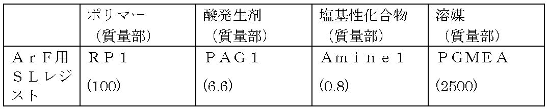
用いたポリマー(RP1)、酸発生剤(PAG1)、及び塩基性化合物(Amine1)の構造式を以下に示す。

液浸保護膜材料(TC-1)としては、保護膜ポリマー(PP1)を有機溶剤中に表10の割合で溶解させ、0.1μmのフッ素樹脂製のフィルターで濾過することによって調製した。 The liquid immersion protective film material (TC-1) was prepared by dissolving the protective film polymer (PP1) in an organic solvent at the ratio shown in Table 10, and filtering it through a 0.1 μm fluororesin filter.

用いたポリマー(PP1)の構造式を以下に示す。

ケイ素含有レジスト下層膜材料(SOG-1)としてはArF珪素含有中間膜ポリマー(SiP1)で示されるポリマー、及び架橋触媒(CAT1)を、FC-4430(住友スリーエム社製)0.1質量%を含む有機溶剤中に表11に示す割合で溶解させ、孔径0.1μmのフッ素樹脂製のフィルターで濾過することによって、ケイ素含有レジスト下層膜材料(SOG-1)を調製した。 As the silicon-containing resist underlayer film material (SOG-1), a polymer represented by ArF silicon-containing interlayer film polymer (SiP1) and a crosslinking catalyst (CAT1) were used, and 0.1% by mass of FC-4430 (manufactured by Sumitomo 3M) was used. A silicon-containing resist underlayer film material (SOG-1) was prepared by dissolving it in the proportion shown in Table 11 in an organic solvent and filtering it through a fluororesin filter with a pore size of 0.1 μm.

用いたArF珪素含有中間膜ポリマー(SiP1)、架橋触媒(CAT1)の構造式を以下に示す。

次いで、ArF液浸露光装置((株)ニコン製;NSR-S610C,NA1.30、σ0.98/0.65、35度ダイポールs偏光照明、6%ハーフトーン位相シフトマスク)で露光量を変えながら露光し、100℃で60秒間ベーク(PEB)し、2.38質量%テトラメチルアンモニウムヒドロキシド(TMAH)水溶液で30秒間現像し、ピッチ100nmでレジスト線幅を50nmから30nmまでのポジ型のラインアンドスペースパターンを得た。 Next, the exposure amount was changed using an ArF immersion exposure device (manufactured by Nikon Corporation; NSR-S610C, NA 1.30, σ 0.98/0.65, 35 degree dipole s polarized illumination, 6% halftone phase shift mask). The resist was exposed to light, baked (PEB) at 100°C for 60 seconds, developed for 30 seconds with a 2.38% by mass tetramethylammonium hydroxide (TMAH) aqueous solution, and the resist line width was changed from 50 nm to 30 nm with a pitch of 100 nm. I got a line and space pattern.
次いで、東京エレクトロン製エッチング装置Teliusを用いてドライエッチングによるレジストパターンをマスクにしてケイ素含有レジスト下層膜の加工、ケイ素含有レジスト下層膜をマスクにして有機膜、有機膜をマスクにしてSiO2膜の加工を行った。 Next, using an etching device Telius manufactured by Tokyo Electron, the silicon-containing resist lower layer film was processed using the dry etching resist pattern as a mask, the silicon-containing resist lower layer film was used as a mask to process an organic film, and the organic film was used as a mask to form a SiO 2 film. Processed.
エッチング条件は下記に示すとおりである。
レジストパターンのSOG膜への転写条件。
チャンバー圧力 10.0Pa
RFパワー 1,500W
CF4ガス流量 15sccm
O2ガス流量 75sccm
時間 15sec
The etching conditions are as shown below.
Conditions for transferring the resist pattern to the SOG film.
Chamber pressure 10.0Pa
RF power 1,500W
CF4 gas flow rate 15sccm
O2 gas flow rate 75sccm
Time 15sec
SOG膜パターンの有機膜への転写条件。
チャンバー圧力 2.0Pa
RFパワー 500W
Arガス流量 75sccm
O2ガス流量 45sccm
時間 120sec
Conditions for transferring the SOG film pattern to the organic film.
Chamber pressure 2.0Pa
RF power 500W
Ar gas flow rate 75sccm
O2 gas flow rate 45sccm
Time 120sec
有機膜パターンのSiO2膜への転写条件。
チャンバー圧力 2.0Pa
RFパワー 2,200W
C5F12ガス流量 20sccm
C2F6ガス流量 10sccm
Arガス流量 300sccm
O2ガス流量 60sccm
時間 90sec
Conditions for transferring an organic film pattern to a SiO 2 film.
Chamber pressure 2.0Pa
RF power 2,200W
C5F12 gas flow rate 20sccm
C2F6 gas flow rate 10sccm
Ar gas flow rate 300sccm
O2 gas flow rate 60sccm
Time 90sec
パターン断面を(株)日立製作所製電子顕微鏡(S-4700)にて観察し、形状を比較し、表12にまとめた。 A cross section of the pattern was observed using an electron microscope (S-4700) manufactured by Hitachi, Ltd., and the shapes were compared and summarized in Table 12.

表12に示されるように、本発明の有機膜形成材料(実施例5-1~5-17)の結果の通り、いずれの場合もレジスト上層膜パターンが最終的に基板まで良好に転写されており、本発明の有機膜形成材料は多層レジスト法による有機膜用の材料として好適に用いられることが確認された。また、露光により作られたレジスト線幅に従って、基板転写後のパターン寸法も変化し、比較例5-1においては40nm程度の線幅でパターンよれが発生したが、本発明の重合体を用いた実施例5-1~5-17においてはパターン寸法35nm以下までよれがなく、高いよれ耐性を有することが判明した。本発明の重合体のように、ハードネスが0.60GPaを超える緻密な高強度の膜が形成できる有機膜を使用することにより高いよれ耐性を得られることがわかる。 As shown in Table 12, as shown in the results of the organic film forming materials of the present invention (Examples 5-1 to 5-17), the resist upper layer film pattern was finally transferred well to the substrate in all cases. Therefore, it was confirmed that the organic film forming material of the present invention can be suitably used as a material for an organic film formed by a multilayer resist method. In addition, the pattern dimensions after transfer to the substrate changed according to the resist line width created by exposure, and in Comparative Example 5-1, pattern waviness occurred at a line width of about 40 nm, but when using the polymer of the present invention, In Examples 5-1 to 5-17, there was no twisting up to a pattern size of 35 nm or less, and it was found that they had high resistance to twisting. It can be seen that high kink resistance can be obtained by using an organic film capable of forming a dense, high-strength film with a hardness exceeding 0.60 GPa, like the polymer of the present invention.
実施例6 平坦化特性評価(実施例6-1~6-12、比較例6-1)
有機膜形成材料(UDL-3、5、6、7、9、11~17、比較UDL-2)をそれぞれ、巨大孤立トレンチパターン(トレンチ幅10μm、トレンチ深さ0.10μm)を有するSiO2基板(図2中の8)上に塗布し、大気中、350℃で60秒間焼成した後、トレンチ部分と非トレンチ部分の有機膜(図2中の7)の段差(図2中のdelta)を、パークシステムズ社製NX10原子間力顕微鏡(AFM)を用いて観察した。結果を表13に示す。本評価において、段差が小さいほど、平坦化特性が良好であるといえる。なお、本評価では、深さ0.10μmのトレンチパターンを、膜厚約0.2μmの有機膜形成材料を用いて平坦化しており、平坦化特性の優劣を評価するために厳しい評価条件となっている。
Example 6 Flattening characteristic evaluation (Examples 6-1 to 6-12, Comparative example 6-1)
The organic film forming materials (UDL-3, 5, 6, 7, 9, 11 to 17, comparative UDL-2) were each placed on a SiO 2 substrate having a giant isolated trench pattern (

表13に示されるように、本発明の有機膜形成材料は、比較例6-1に比べてトレンチ部分と非トレンチ部分の有機膜の段差が小さく、平坦化特性に優れることが確認された。これは実施例2の通り、本発明の重合体は耐熱性に優れるためベークによる膜のシュリンクが抑制されていることに起因する。また、高沸点溶剤を添加した実施例6-7~6-12と添加していない実施例6-1~6-6とを比較すると高沸点溶剤の添加により平坦性が改善していることがわかる。 As shown in Table 13, it was confirmed that the organic film forming material of the present invention had a smaller step difference between the organic film in the trench portion and the non-trench portion than in Comparative Example 6-1, and had excellent planarization properties. This is because, as in Example 2, the polymer of the present invention has excellent heat resistance, and therefore shrinkage of the film due to baking is suppressed. Furthermore, when comparing Examples 6-7 to 6-12 in which high-boiling point solvents were added and Examples 6-1 to 6-6 in which no high-boiling point solvents were added, it was found that the flatness was improved by the addition of high-boiling point solvents. Recognize.
以上のように、本発明の有機膜形成材料は、耐熱性、高いエッチング耐性、エッチング時のよれ耐性に優れており、超微細かつ高精度なパターン加工のための多層レジストプロセス、特に3層レジストプロセス用有機膜として極めて有用である。 As described above, the organic film-forming material of the present invention has excellent heat resistance, high etching resistance, and resistance to twisting during etching, and can be used in multilayer resist processes for ultra-fine and high-precision pattern processing, especially in three-layer resists. It is extremely useful as an organic film for processing.
1…基板、 2…被加工層、 2a…基板に形成されるパターン、
3…有機膜、 3a…有機膜パターン、 4…ケイ素含有レジスト下層膜、
4a…ケイ素含有レジスト下層膜パターン、 5…レジスト上層膜、
5a…レジストパターン、 6…所用部分、 7…有機膜、 8…SiO2基板
delta…段差
1... Substrate, 2... Layer to be processed, 2a... Pattern formed on the substrate,
3...Organic film, 3a...Organic film pattern, 4...Silicon-containing resist lower layer film,
4a...Silicon-containing resist lower layer film pattern, 5...Resist upper layer film,
5a...Resist pattern, 6...Required portion, 7...Organic film, 8...SiO 2 substrate delta...Step
Claims (20)


被加工基板上に請求項1から請求項7のいずれか一項に記載の有機膜形成材料を用いて有機膜を形成し、該有機膜の上にケイ素含有レジスト下層膜材料を用いてケイ素含有レジスト下層膜を形成し、該ケイ素含有レジスト下層膜の上にフォトレジスト組成物を用いてレジスト上層膜を形成し、該レジスト上層膜に回路パターンを形成し、該パターンが形成されたレジスト上層膜をマスクにして前記ケイ素含有レジスト下層膜にエッチングでパターン転写し、該パターンが転写されたケイ素含有レジスト下層膜をマスクにして前記有機膜にエッチングでパターン転写し、さらに、該パターンが転写された有機膜をマスクにして前記被加工基板にエッチングでパターンを形成することを特徴とするパターン形成方法。 A method of forming a pattern on a processed substrate, the method comprising:
An organic film is formed on a substrate to be processed using the organic film forming material according to any one of claims 1 to 7, and a silicon-containing resist underlayer film material is used on the organic film to form a silicon-containing resist underlayer film material. forming a resist lower layer film, forming a resist upper layer film using a photoresist composition on the silicon-containing resist lower layer film, forming a circuit pattern on the resist upper layer film, and resist upper layer film having the pattern formed thereon; A pattern is transferred by etching to the silicon-containing resist underlayer film using as a mask, a pattern is transferred to the organic film by etching using the silicon-containing resist underlayer film to which the pattern is transferred as a mask, and further, the pattern is transferred. A pattern forming method comprising forming a pattern on the substrate to be processed by etching using an organic film as a mask.
被加工基板上に請求項1から請求項7のいずれか一項に記載の有機膜形成材料を用いて有機膜を形成し、該有機膜の上にケイ素含有レジスト下層膜材料を用いてケイ素含有レジスト下層膜を形成し、該ケイ素含有レジスト下層膜の上に有機反射防止膜(BARC)を形成し、該BARC上にフォトレジスト組成物を用いてレジスト上層膜を形成して4層膜構造とし、該レジスト上層膜に回路パターンを形成し、該パターンが形成されたレジスト上層膜をマスクにして前記BARC膜と前記ケイ素含有レジスト下層膜にエッチングでパターン転写し、該パターンが転写されたケイ素含有レジスト下層膜をマスクにして前記有機膜にエッチングでパターン転写し、さらに、該パターンが転写された有機膜をマスクにして前記被加工基板をエッチングして該被加工基板にパターンを形成することを特徴とするパターン形成方法。 A method of forming a pattern on a processed substrate, the method comprising:
An organic film is formed on a substrate to be processed using the organic film forming material according to any one of claims 1 to 7, and a silicon-containing resist underlayer film material is used on the organic film to form a silicon-containing resist underlayer film material. A resist lower layer film is formed, an organic antireflection coating (BARC) is formed on the silicon-containing resist lower layer film, and a resist upper layer film is formed using a photoresist composition on the BARC to form a four-layer film structure. , a circuit pattern is formed on the resist upper layer film, the pattern is transferred by etching to the BARC film and the silicon-containing resist lower layer film using the resist upper layer film on which the pattern is formed as a mask, and the silicon-containing resist film to which the pattern is transferred is etched. Transferring a pattern to the organic film by etching using the resist underlayer film as a mask, and etching the substrate to be processed using the organic film to which the pattern has been transferred as a mask to form a pattern on the substrate to be processed. Characteristic pattern formation method.
被加工基板上に請求項1から請求項7のいずれか一項に記載の有機膜形成材料を用いて有機膜を形成し、該有機膜の上にケイ素酸化膜、ケイ素窒化膜、ケイ素酸化窒化膜から選ばれる無機ハードマスクを形成し、該無機ハードマスクの上にフォトレジスト組成物を用いてレジスト上層膜を形成して、該レジスト上層膜に回路パターンを形成し、該パターンが形成されたレジスト上層膜をマスクにして前記無機ハードマスクにエッチングでパターンを転写し、該パターンが転写された無機ハードマスクをマスクにして前記有機膜にエッチングでパターンを転写し、さらに、該パターンが転写された有機膜をマスクにして前記被加工基板をエッチングして該被加工基板にパターンを形成することを特徴とするパターン形成方法。 A method of forming a pattern on a processed substrate, the method comprising:
An organic film is formed on a substrate to be processed using the organic film forming material according to any one of claims 1 to 7, and a silicon oxide film, a silicon nitride film, a silicon oxynitride film is formed on the organic film. forming an inorganic hard mask selected from the films, forming a resist upper layer film using a photoresist composition on the inorganic hard mask, forming a circuit pattern on the resist upper layer film, and forming the pattern. A pattern is transferred by etching to the inorganic hard mask using the resist upper layer film as a mask, a pattern is transferred to the organic film by etching using the inorganic hard mask to which the pattern has been transferred as a mask, and further, the pattern is transferred. A pattern forming method comprising etching the substrate to be processed using an organic film as a mask to form a pattern on the substrate to be processed.
被加工基板上に請求項1から請求項7のいずれか一項に記載の有機膜形成材料を用いて有機膜を形成し、該有機膜の上にケイ素酸化膜、ケイ素窒化膜、ケイ素酸化窒化膜から選ばれる無機ハードマスクを形成し、該無機ハードマスクの上に有機反射防止膜(BARC)を形成し、該BARC上にフォトレジスト組成物を用いてレジスト上層膜を形成して4層膜構造とし、該レジスト上層膜に回路パターンを形成し、該パターンが形成されたレジスト上層膜をマスクにして前記BARC膜と前記無機ハードマスクにエッチングでパターンを転写し、該パターンが転写された無機ハードマスクをマスクにして前記有機膜にエッチングでパターンを転写し、さらに、該パターンが転写された有機膜をマスクにして前記被加工基板をエッチングして該被加工基板にパターンを形成することを特徴とするパターン形成方法。 A method of forming a pattern on a processed substrate, the method comprising:
An organic film is formed on a substrate to be processed using the organic film forming material according to any one of claims 1 to 7, and a silicon oxide film, a silicon nitride film, a silicon oxynitride film is formed on the organic film. An inorganic hard mask selected from the above films is formed, an organic anti-reflection coating (BARC) is formed on the inorganic hard mask, and a resist upper layer film is formed using a photoresist composition on the BARC to form a four-layer film. A circuit pattern is formed on the resist upper layer film, and the pattern is transferred by etching to the BARC film and the inorganic hard mask using the resist upper layer film with the pattern formed as a mask. Transferring a pattern to the organic film by etching using a hard mask as a mask, and etching the substrate to be processed using the organic film to which the pattern has been transferred as a mask to form a pattern on the substrate to be processed. Characteristic pattern formation method.


The polymer according to any one of claims 17 to 19, wherein the terminal structure of the polymer is one of the following general formulas (6) and (7).
Priority Applications (6)
| Application Number | Priority Date | Filing Date | Title |
|---|---|---|---|
| JP2020217018A JP7401424B2 (en) | 2020-12-25 | 2020-12-25 | Organic film-forming materials, pattern-forming methods, and polymers |
| US17/549,987 US20220214618A1 (en) | 2020-12-25 | 2021-12-14 | Material for forming organic film, patterning process, and polymer |
| EP21214858.9A EP4020083A1 (en) | 2020-12-25 | 2021-12-15 | Material for forming organic film, patterning process, and polymer |
| KR1020210184057A KR20220092803A (en) | 2020-12-25 | 2021-12-21 | Material for forming organic film, patterning process, and polymer |
| TW110148118A TWI801052B (en) | 2020-12-25 | 2021-12-22 | Material for forming organic film, patterning process, and polymer |
| CN202111600298.6A CN114690555A (en) | 2020-12-25 | 2021-12-24 | Organic film forming material, pattern forming method and polymer |
Applications Claiming Priority (1)
| Application Number | Priority Date | Filing Date | Title |
|---|---|---|---|
| JP2020217018A JP7401424B2 (en) | 2020-12-25 | 2020-12-25 | Organic film-forming materials, pattern-forming methods, and polymers |
Publications (2)
| Publication Number | Publication Date |
|---|---|
| JP2022102339A JP2022102339A (en) | 2022-07-07 |
| JP7401424B2 true JP7401424B2 (en) | 2023-12-19 |
Family
ID=79024346
Family Applications (1)
| Application Number | Title | Priority Date | Filing Date |
|---|---|---|---|
| JP2020217018A Active JP7401424B2 (en) | 2020-12-25 | 2020-12-25 | Organic film-forming materials, pattern-forming methods, and polymers |
Country Status (6)
| Country | Link |
|---|---|
| US (1) | US20220214618A1 (en) |
| EP (1) | EP4020083A1 (en) |
| JP (1) | JP7401424B2 (en) |
| KR (1) | KR20220092803A (en) |
| CN (1) | CN114690555A (en) |
| TW (1) | TWI801052B (en) |
Families Citing this family (2)
| Publication number | Priority date | Publication date | Assignee | Title |
|---|---|---|---|---|
| JP7161451B2 (en) * | 2019-07-05 | 2022-10-26 | 信越化学工業株式会社 | Composition for forming organic film, substrate for manufacturing semiconductor device, method for forming organic film, and method for forming pattern |
| WO2024070728A1 (en) * | 2022-09-30 | 2024-04-04 | Jsr株式会社 | Method for producing semiconductor substrate, composition and polymer |
Citations (3)
| Publication number | Priority date | Publication date | Assignee | Title |
|---|---|---|---|---|
| JP2014145088A (en) | 2009-10-28 | 2014-08-14 | Transitions Optical Inc | Photochromic material |
| WO2017208796A1 (en) | 2016-06-03 | 2017-12-07 | Jsr株式会社 | Composition for forming film, film, method for forming resist underlayer film, method for manufacturing patterned substrate, and compound |
| JP2019172605A (en) | 2018-03-28 | 2019-10-10 | 信越化学工業株式会社 | Compound, composition for forming organic film, substrate for manufacturing semiconductor device, method of forming organic film, and method of forming pattern |
Family Cites Families (18)
| Publication number | Priority date | Publication date | Assignee | Title |
|---|---|---|---|---|
| JP2657740B2 (en) | 1992-10-08 | 1997-09-24 | 日本電信電話株式会社 | Positive resist material |
| JP3774668B2 (en) | 2001-02-07 | 2006-05-17 | 東京エレクトロン株式会社 | Cleaning pretreatment method for silicon nitride film forming apparatus |
| JP3981825B2 (en) | 2002-12-24 | 2007-09-26 | 信越化学工業株式会社 | Pattern forming method and lower layer film forming material |
| JP4382750B2 (en) | 2003-01-24 | 2009-12-16 | 東京エレクトロン株式会社 | CVD method for forming a silicon nitride film on a substrate to be processed |
| GB2424895B (en) * | 2003-10-01 | 2008-07-09 | Sumitomo Chemical Co | Polymer light-emitting material and polymer light-emitting device |
| JP4355943B2 (en) | 2003-10-03 | 2009-11-04 | 信越化学工業株式会社 | Photoresist underlayer film forming material and pattern forming method |
| JP4388429B2 (en) | 2004-02-04 | 2009-12-24 | 信越化学工業株式会社 | Resist underlayer film material and pattern forming method |
| JP4496432B2 (en) | 2005-02-18 | 2010-07-07 | 信越化学工業株式会社 | Photoresist underlayer film forming material and pattern forming method |
| JP4662052B2 (en) | 2005-03-11 | 2011-03-30 | 信越化学工業株式会社 | Photoresist underlayer film forming material and pattern forming method |
| JP4575214B2 (en) | 2005-04-04 | 2010-11-04 | 信越化学工業株式会社 | Resist underlayer film material and pattern forming method |
| JP4659678B2 (en) | 2005-12-27 | 2011-03-30 | 信越化学工業株式会社 | Photoresist underlayer film forming material and pattern forming method |
| JP2008158002A (en) | 2006-12-20 | 2008-07-10 | Jsr Corp | Composition for resist underlayer film, and its manufacturing method |
| JP4569786B2 (en) | 2008-05-01 | 2010-10-27 | 信越化学工業株式会社 | Novel photoacid generator, resist material and pattern forming method using the same |
| JP5336306B2 (en) | 2008-10-20 | 2013-11-06 | 信越化学工業株式会社 | Resist underlayer film forming method, pattern forming method using the same, and resist underlayer film material |
| US20140246400A1 (en) | 2011-09-30 | 2014-09-04 | Mitsubishi Gas Chemical Company, Inc. | Resin having fluorene structure and material for forming underlayer film for lithography |
| JP5925721B2 (en) | 2012-05-08 | 2016-05-25 | 信越化学工業株式会社 | Organic film material, organic film forming method and pattern forming method using the same |
| KR101781739B1 (en) * | 2015-10-07 | 2017-09-25 | 주식회사 엘지화학 | New compound and organic light emitting device comprising the same |
| JP7082087B2 (en) * | 2019-05-08 | 2022-06-07 | 信越化学工業株式会社 | Organic film forming composition, pattern forming method and polymer |
-
2020
- 2020-12-25 JP JP2020217018A patent/JP7401424B2/en active Active
-
2021
- 2021-12-14 US US17/549,987 patent/US20220214618A1/en active Pending
- 2021-12-15 EP EP21214858.9A patent/EP4020083A1/en active Pending
- 2021-12-21 KR KR1020210184057A patent/KR20220092803A/en active IP Right Grant
- 2021-12-22 TW TW110148118A patent/TWI801052B/en active
- 2021-12-24 CN CN202111600298.6A patent/CN114690555A/en active Pending
Patent Citations (3)
| Publication number | Priority date | Publication date | Assignee | Title |
|---|---|---|---|---|
| JP2014145088A (en) | 2009-10-28 | 2014-08-14 | Transitions Optical Inc | Photochromic material |
| WO2017208796A1 (en) | 2016-06-03 | 2017-12-07 | Jsr株式会社 | Composition for forming film, film, method for forming resist underlayer film, method for manufacturing patterned substrate, and compound |
| JP2019172605A (en) | 2018-03-28 | 2019-10-10 | 信越化学工業株式会社 | Compound, composition for forming organic film, substrate for manufacturing semiconductor device, method of forming organic film, and method of forming pattern |
Also Published As
| Publication number | Publication date |
|---|---|
| TW202235477A (en) | 2022-09-16 |
| EP4020083A1 (en) | 2022-06-29 |
| CN114690555A (en) | 2022-07-01 |
| KR20220092803A (en) | 2022-07-04 |
| JP2022102339A (en) | 2022-07-07 |
| TWI801052B (en) | 2023-05-01 |
| US20220214618A1 (en) | 2022-07-07 |
Similar Documents
| Publication | Publication Date | Title |
|---|---|---|
| JP7209588B2 (en) | Organic film forming composition, pattern forming method and polymer | |
| JP7406590B2 (en) | polymer | |
| KR102274471B1 (en) | Composition for forming organic film, patterning process, and polymer | |
| KR102474405B1 (en) | Composition for forming organic film, patterning process and polymer | |
| JP7401424B2 (en) | Organic film-forming materials, pattern-forming methods, and polymers | |
| KR102619778B1 (en) | Material for forming organic film, patterning process, compound, and polymer | |
| KR102353266B1 (en) | Composition for forming organic film, patterning process, and polymer | |
| JP2019023251A (en) | Organic film forming composition, patterning method, and organic film forming resin | |
| JP7465679B2 (en) | Coating-type organic film-forming composition, pattern forming method, polymer, and method for producing polymer | |
| JP2023128578A (en) | Composition for forming organic film, patterning method, and compound | |
| JP2023074248A (en) | Composition for forming organic film, patterning process, and compound and polymer for forming organic film |
Legal Events
| Date | Code | Title | Description |
|---|---|---|---|
| A621 | Written request for application examination |
Free format text: JAPANESE INTERMEDIATE CODE: A621 Effective date: 20221221 |
|
| A977 | Report on retrieval |
Free format text: JAPANESE INTERMEDIATE CODE: A971007 Effective date: 20231024 |
|
| TRDD | Decision of grant or rejection written | ||
| A01 | Written decision to grant a patent or to grant a registration (utility model) |
Free format text: JAPANESE INTERMEDIATE CODE: A01 Effective date: 20231114 |
|
| A61 | First payment of annual fees (during grant procedure) |
Free format text: JAPANESE INTERMEDIATE CODE: A61 Effective date: 20231207 |
|
| R150 | Certificate of patent or registration of utility model |
Ref document number: 7401424 Country of ref document: JP Free format text: JAPANESE INTERMEDIATE CODE: R150 |