JP4355943B2 - Photoresist underlayer film forming material and pattern forming method - Google Patents
Photoresist underlayer film forming material and pattern forming method Download PDFInfo
- Publication number
- JP4355943B2 JP4355943B2 JP2004278933A JP2004278933A JP4355943B2 JP 4355943 B2 JP4355943 B2 JP 4355943B2 JP 2004278933 A JP2004278933 A JP 2004278933A JP 2004278933 A JP2004278933 A JP 2004278933A JP 4355943 B2 JP4355943 B2 JP 4355943B2
- Authority
- JP
- Japan
- Prior art keywords
- group
- layer
- film
- derivatives
- photoresist
- Prior art date
- Legal status (The legal status is an assumption and is not a legal conclusion. Google has not performed a legal analysis and makes no representation as to the accuracy of the status listed.)
- Active
Links
- XBTKDTQCOLSJCJ-UHFFFAOYSA-N CC[S+](C#CC)[F](C)C Chemical compound CC[S+](C#CC)[F](C)C XBTKDTQCOLSJCJ-UHFFFAOYSA-N 0.000 description 1
Images


Description
本発明は、半導体素子などの製造工程における微細加工に用いられる多層レジスト工程において有効な下層膜形成材料及びこれを用いた遠紫外線、KrFエキシマレーザー光、ArFエキシマレーザー光(193nm)、F2レーザー光(157nm)、Kr2レーザー光(146nm)、Ar2レーザー光(126nm)、軟X線、電子ビーム、イオンビーム、X線露光に好適なレジストパターン形成方法に関するものである。 The present invention relates to an underlayer film forming material effective in a multilayer resist process used for microfabrication in a manufacturing process of a semiconductor element and the like, and far ultraviolet rays, KrF excimer laser light, ArF excimer laser light (193 nm), F 2 laser using the material. The present invention relates to a resist pattern forming method suitable for light (157 nm), Kr 2 laser light (146 nm), Ar 2 laser light (126 nm), soft X-ray, electron beam, ion beam, and X-ray exposure.
近年、LSIの高集積化と高速度化に伴い、パターンルールの微細化が求められている中、現在汎用技術として用いられている光露光を用いたリソグラフィーにおいては、光源の波長に由来する本質的な解像度の限界に近づきつつある。 In recent years, with the increasing integration and speed of LSIs, there is a need for finer pattern rules. In lithography using light exposure, which is currently used as a general-purpose technology, the essence derived from the wavelength of the light source The resolution limit is approaching.
レジストパターン形成の際に使用するリソグラフィー用の光源として、水銀灯のg線(436nm)もしくはi線(365nm)を光源とする光露光が広く用いられており、更なる微細化のための手段として、露光光を短波長化する方法が有効とされてきた。このため、64MビットDRAM加工方法の量産プロセスには、露光光源としてi線(365nm)に代わって短波長のKrFエキシマレーザー(248nm)が利用された。しかし、更に微細な加工技術(加工寸法が0.13μm以下)を必要とする集積度1G以上のDRAMの製造には、より短波長の光源が必要とされ、特にArFエキシマレーザー(193nm)を用いたリソグラフィーが検討されてきている。 As a light source for lithography used in forming a resist pattern, light exposure using a mercury lamp g-line (436 nm) or i-line (365 nm) as a light source is widely used, and as a means for further miniaturization, A method of shortening the wavelength of exposure light has been considered effective. For this reason, a short wavelength KrF excimer laser (248 nm) was used as an exposure light source in place of the i-line (365 nm) in the mass production process of the 64-Mbit DRAM processing method. However, in order to manufacture a DRAM having a degree of integration of 1G or more, which requires a finer processing technique (processing dimension is 0.13 μm or less), a light source with a shorter wavelength is required, and in particular, an ArF excimer laser (193 nm) is used. Lithography has been studied.
一方、従来、段差基板上に高アスペクト比のパターンを形成するには2層レジスト法が優れていることが知られており、更に、2層レジスト膜を一般的なアルカリ現像液で現像するためには、ヒドロキシ基やカルボキシル基等の親水基を有する高分子シリコーン化合物が必要である。 On the other hand, conventionally, it is known that a two-layer resist method is excellent for forming a pattern with a high aspect ratio on a stepped substrate, and further, a two-layer resist film is developed with a general alkaline developer. Requires a high molecular silicone compound having a hydrophilic group such as a hydroxy group or a carboxyl group.
シリコーン系化学増幅ポジ型レジスト材料としては、安定なアルカリ可溶性シリコーンポリマーであるポリヒドロキシベンジルシルセスキオキサンのフェノール性水酸基の一部をt−Boc基で保護したものをベース樹脂として使用し、これと酸発生剤とを組み合わせたKrFエキシマレーザー用シリコーン系化学増幅ポジ型レジスト材料が提案された(特許文献2:特開平6−118651号公報、非特許文献1:SPIE vol.1925(1993) p377等参照)。また、ArFエキシマレーザー用としては、シクロヘキシルカルボン酸を酸不安定基で置換したタイプのシルセスキオキサンをベースにしたポジ型レジストが提案されている(特許文献3、4:特開平10−324748号公報、特開平11−302382号公報、非特許文献2:SPIE vol.3333(1998) p62参照)。更に、F2レーザー用としては、ヘキサフルオロイソプロパノールを溶解性基として持つシルセスキオキサンをベースにしたポジ型レジストが提案されている(特許文献5:特開2002−55456号公報)。上記ポリマーは、トリアルコキシシシラン、又はトリハロゲン化シランの縮重合によるラダー骨格を含むポリシルセスキオキサンを主鎖に含むものである。
As the silicone-based chemically amplified positive resist material, a base resin in which a part of the phenolic hydroxyl group of polyhydroxybenzylsilsesquioxane, which is a stable alkali-soluble silicone polymer, is protected with a t-Boc group is used. And a silicon-based chemically amplified positive resist material for KrF excimer lasers in which an acid generator is combined (Patent Document 2: JP-A-6-118651, Non-Patent Document 1: SPIE vol. 1925 (1993) p377 Etc.). For ArF excimer lasers, positive resists based on silsesquioxane in which cyclohexylcarboxylic acid is substituted with an acid labile group have been proposed (
珪素が側鎖にペンダントされたレジスト用ベースポリマーとしては、珪素含有(メタ)アクリルエステル系ポリマーが提案されている(特許文献6:特開平9−110938号公報、非特許文献3:J. Photopolymer Sci. and Technol. Vol. 9 No.3(1996) p435−446参照)。 Silicon-containing (meth) acrylic ester-based polymers have been proposed as resist base polymers in which silicon is pendant to the side chain (Patent Document 6: Japanese Patent Laid-Open No. 9-110938, Non-Patent Document 3: J. Photopolymer). Sci. And Technol., Vol. 9 No. 3 (1996) p435-446).
2層レジスト法の下層膜としては、酸素ガスによるエッチングが可能な炭化水素化合物であり、更にその下の基板をエッチングする場合におけるマスクになるため、高いエッチング耐性を有することが必要である。酸素ガスエッチングにおいては、珪素原子を含まない炭化水素のみで構成される必要がある。また、上層の珪素含有レジストの線幅制御性を向上させ、定在波によるパターン側壁の凹凸とパターンの崩壊を低減させるためには、反射防止膜としての機能も有し、具体的には下層膜からレジスト膜内への反射率を1%以下に抑える必要がある。 The lower layer film of the two-layer resist method is a hydrocarbon compound that can be etched with oxygen gas, and further serves as a mask when etching the underlying substrate, and therefore needs to have high etching resistance. In oxygen gas etching, it is necessary to be composed only of hydrocarbons that do not contain silicon atoms. In addition, in order to improve the line width controllability of the upper-layer silicon-containing resist and reduce pattern sidewall irregularities and pattern collapse due to standing waves, it also has a function as an antireflection film, specifically the lower layer It is necessary to suppress the reflectance from the film into the resist film to 1% or less.
ここで、最大500nmの膜厚までの反射率を計算した結果を図1、2に示す。露光波長は193nm、上層レジストのn値を1.74、k値を0.02と仮定し、図1では下層膜のk値を0.3に固定し、縦軸にn値を1.0〜2.0、横軸に膜厚0〜500nmの範囲で変動させたときの基板反射率を示す。膜厚が300nm以上の2層レジスト用下層膜を想定した場合、上層レジストと同程度かあるいはそれよりも少し屈折率が高い1.6〜1.9の範囲で反射率を1%以下にできる最適値が存在する。 Here, the result of calculating the reflectance up to a maximum film thickness of 500 nm is shown in FIGS. Assuming that the exposure wavelength is 193 nm, the n value of the upper layer resist is 1.74, and the k value is 0.02, the k value of the lower layer film is fixed at 0.3 in FIG. -2.0, the horizontal axis represents the substrate reflectance when the film thickness is varied in the range of 0 to 500 nm. Assuming a lower layer film for a two-layer resist having a film thickness of 300 nm or more, the reflectance can be reduced to 1% or less in the range of 1.6 to 1.9, which is the same as or slightly higher than the upper layer resist. An optimal value exists.
図2では、下層膜のn値を1.5に固定し、k値を0.1〜0.8の範囲で変動させたときの反射率を示す。k値が0.24〜0.15の範囲で反射率を1%以下にすることが可能である。一方、40nm程度の薄膜で用いられる単層レジスト用の反射防止膜の最適k値は0.4〜0.5であり、300nm以上で用いられる2層レジスト用下層の最適k値とは異なる。2層レジスト用下層では、より低いk値、即ちより高透明な下層膜が必要であることが示されている。 FIG. 2 shows the reflectance when the n value of the lower layer film is fixed to 1.5 and the k value is varied in the range of 0.1 to 0.8. The reflectance can be reduced to 1% or less when the k value is in the range of 0.24 to 0.15. On the other hand, the optimum k value of the antireflection film for a single layer resist used in a thin film of about 40 nm is 0.4 to 0.5, which is different from the optimum k value of the lower layer for a two layer resist used at 300 nm or more. It has been shown that a lower layer for a two-layer resist requires a lower k value, that is, a higher transparent lower layer film.
ここで、193nm用の下層膜形成材料として、SPIE Vol.4345(2001) p50(非特許文献4)に紹介されているようにポリヒドロキシスチレンとアクリルの共重合体が検討されている。ポリヒドロキシスチレンは193nmに非常に強い吸収を持ち、そのもの単独ではk値が0.6前後と高い値である。そこで、k値が殆ど0であるアクリルと共重合させることによって、k値を0.25前後に調整しているのである。 Here, as an underlayer film forming material for 193 nm, SPIE Vol. 4345 (2001) p50 (Non-Patent Document 4), a copolymer of polyhydroxystyrene and acrylic has been studied. Polyhydroxystyrene has a very strong absorption at 193 nm, and the k value alone is a high value of around 0.6. Therefore, the k value is adjusted to around 0.25 by copolymerizing with acrylic whose k value is almost zero.
しかしながら、ポリヒドロキシスチレンに対して、アクリルの基板エッチングにおけるエッチング耐性は弱く、しかもk値を下げるためにかなりの割合のアクリルを共重合せざるを得ず、結果的に基板エッチングの耐性はかなり低下する。エッチングの耐性は、エッチング速度だけでなく、エッチング後の表面ラフネスの発生にも現れてくる。アクリルの共重合によってエッチング後の表面ラフネスの増大が深刻なほど顕著になっている。 However, with respect to polyhydroxystyrene, the etching resistance of acrylic on the substrate etching is weak, and in order to lower the k value, a considerable proportion of acrylic must be copolymerized, resulting in a considerable decrease in the resistance of substrate etching. To do. The resistance to etching appears not only in the etching rate but also in the occurrence of surface roughness after etching. The increase in surface roughness after etching becomes more prominent as a result of acrylic copolymerization.
ベンゼン環よりも193nmにおける透明性が高く、エッチング耐性が高いものの一つにナフタレン環がある。特開2002−14474号公報(特許文献12)にナフタレン環、アントラセン環を有する下層膜が提案されている。しかしながら、ナフトール共縮合ノボラック樹脂、ポリビニルナフタレン樹脂のk値は0.3〜0.4の間であり、目標の0.1〜0.3の透明性には未達であり、更に透明性を上げなくてはならない。また、ナフトール共縮合ノボラック樹脂、ポリビニルナフタレン樹脂の193nmにおけるn値は低く、本発明者らの測定した結果では、ナフトール共縮合ノボラック樹脂で1.4、ポリビニルナフタレン樹脂に至っては1.2である。特開2001−40293号(特許文献13)、特開2002−214777号公報(特許文献14)で示されるアセナフチレン重合体においても、波長248nmに比べて193nmにおけるn値が低く、k値は高く、共に目標値には達していない。n値が高く、k値が低く透明でかつエッチング耐性が高い下層膜が求められている。 One of the ones having higher transparency at 193 nm and higher etching resistance than a benzene ring is a naphthalene ring. Japanese Unexamined Patent Application Publication No. 2002-14474 (Patent Document 12) proposes a lower layer film having a naphthalene ring and an anthracene ring. However, the k value of naphthol co-condensed novolak resin and polyvinyl naphthalene resin is between 0.3 and 0.4, and the target transparency of 0.1 to 0.3 has not been achieved. I have to raise it. Further, the n value at 193 nm of the naphthol co-condensed novolak resin and the polyvinyl naphthalene resin is low, and as a result of measurement by the present inventors, it is 1.4 for the naphthol co-condensed novolak resin and 1.2 for the polyvinyl naphthalene resin. . Also in the acenaphthylene polymer shown by Unexamined-Japanese-Patent No. 2001-40293 (patent document 13) and Unexamined-Japanese-Patent No. 2002-214777 (patent document 14), the n value in 193 nm is low compared with wavelength 248 nm, k value is high, Both have not reached the target value. There is a need for a lower layer film that has a high n value, a low k value, is transparent, and has high etching resistance.
一方、珪素を含まない単層レジストを上層、その下に珪素を含有する中間層、更にその下に有機膜を積層する3層プロセスが提案されている(非特許文献5:J.Vac.Sci.Technol.,16(6),Nov./Dec.1979参照)。
一般的には珪素含有レジストより単層レジストの方が解像性に優れ、3層プロセスでは高解像な単層レジストを露光イメージング層として用いることができる。
中間層としては、スピンオングラス(SOG)膜が用いられ、多くのSOG膜が提案されている。
On the other hand, a three-layer process has been proposed in which a single-layer resist containing no silicon is formed as an upper layer, an intermediate layer containing silicon underneath, and an organic film thereunder (Non-Patent Document 5: J. Vac. Sci). Technol., 16 (6), Nov./Dec. 1979).
In general, a single-layer resist has better resolution than a silicon-containing resist, and a high-resolution single-layer resist can be used as an exposure imaging layer in a three-layer process.
As the intermediate layer, a spin-on-glass (SOG) film is used, and many SOG films have been proposed.
ここで3層プロセスにおける基板反射を抑えるための最適な下層膜の光学定数は2層プロセスにおけるそれとは異なっている。
基板反射をできるだけ抑え、具体的には1%以下にまで低減させる目的は2層プロセスも3層プロセスも変わらないのであるが、2層プロセスは下層膜だけに反射防止効果を持たせるのに対して、3層プロセスは中間層と下層のどちらか一方あるいは両方に反射防止効果を持たせることができる。
反射防止効果を付与させた珪素含有層材料が、米国特許第6506497号明細書(特許文献9)、米国特許第6420088号明細書(特許文献10)に提案されている。
一般的に単層の反射防止膜よりも多層反射防止膜の方が反射防止効果が高く、光学材料の反射防止膜として広く工業的に用いられている。
中間層と下層の両方に反射防止効果を付与させることによって高い反射防止効果を得ることができる。
3層プロセスにおいて珪素含有中間層に反射防止膜としての機能を持たせることができれば、下層膜に反射防止膜としての最高の効果は特に必要がない。
3層プロセスの場合の下層膜としては、反射防止膜としての効果よりも基板加工における高いエッチング耐性が要求される。
そのために、エッチング耐性が高く、芳香族基を多く含有するノボラック樹脂を3層プロセス用下層膜として用いることが必要である。
Here, the optimum optical constant of the lower layer film for suppressing the substrate reflection in the three-layer process is different from that in the two-layer process.
The purpose of suppressing the substrate reflection as much as possible, specifically to reduce it to 1% or less, is the same in both the two-layer process and the three-layer process, whereas the two-layer process has an antireflection effect only on the lower layer film. In the three-layer process, one or both of the intermediate layer and the lower layer can have an antireflection effect.
A silicon-containing layer material imparted with an antireflection effect is proposed in US Pat. No. 6,506,497 (Patent Document 9) and US Pat. No. 6420088 (Patent Document 10).
In general, a multilayer antireflection film has a higher antireflection effect than a single-layer antireflection film, and is widely used industrially as an antireflection film for optical materials.
By giving an antireflection effect to both the intermediate layer and the lower layer, a high antireflection effect can be obtained.
If the silicon-containing intermediate layer can be provided with a function as an antireflection film in the three-layer process, the lower layer film does not need the highest effect as the antireflection film.
As a lower layer film in the case of a three-layer process, higher etching resistance in substrate processing is required than an effect as an antireflection film.
Therefore, it is necessary to use a novolak resin having high etching resistance and containing many aromatic groups as a lower layer film for a three-layer process.
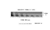
ここで、図3に中間層のk値を変化させたときの基板反射率を示す。
中間層のk値として0.2以下の低い値と、適切な膜厚設定によって、1%以下の十分な反射防止効果を得ることができる。
通常反射防止膜として、膜厚100nm以下で反射を1%に抑ええるためにはk値が0.2以上が必要であるが(図2参照)、下層膜である程度の反射を抑ええることができる3層構造の中間層としては0.2より低い値のk値が最適値となる。
次に下層膜のk値が0.2の場合と0.6の場合の、中間層と下層の膜厚を変化させたときの反射率変化を図4と5に示す。
k値が0.2の下層は、2層プロセスに最適化された下層膜を想定しており、k値が0.6の下層は、193nmにおけるノボラックやポリヒドロキシスチレンのk値に近い値である。
下層膜の膜厚は基板のトポグラフィーによって変動するが、中間層の膜厚はほとんど変動せず、設定した膜厚で塗布できると考えられる。
ここで、下層膜のk値が高い方(0.6の場合)が、より薄膜で反射を1%以下に抑えることができる。
下層膜のk値が0.2の場合、250nm膜厚では反射を1%にするために中間層の膜厚を厚くしなければならない。
中間層の膜厚を上げると、中間層を加工するときのドライエッチング時に最上層のレジストに対する負荷が大きく、好ましいことではない。
下層膜を薄膜で用いるためには、高いk値だけでなく、より強いエッチング耐性が必要である。
Here, FIG. 3 shows the substrate reflectivity when the k value of the intermediate layer is changed.
A sufficient antireflection effect of 1% or less can be obtained by a low value of 0.2 or less as the k value of the intermediate layer and an appropriate film thickness setting.
As an antireflection film, a k value of 0.2 or more is necessary in order to suppress the reflection to 1% when the film thickness is 100 nm or less (see FIG. 2). As an intermediate layer having a three-layer structure, an optimum value is k value lower than 0.2.
Next, FIGS. 4 and 5 show the reflectance change when the thickness of the intermediate layer and the lower layer is changed when the k value of the lower layer film is 0.2 and 0.6.
The lower layer with a k value of 0.2 assumes a lower layer film optimized for a two-layer process, and the lower layer with a k value of 0.6 is close to the k value of novolak or polyhydroxystyrene at 193 nm. is there.
Although the film thickness of the lower layer film varies depending on the topography of the substrate, the film thickness of the intermediate layer hardly varies, and it can be considered that the film can be applied with a set film thickness.
Here, the higher the k value of the lower layer film (in the case of 0.6), the reflection can be suppressed to 1% or less with a thinner film.
When the k value of the lower layer film is 0.2, the film thickness of the intermediate layer must be increased in order to obtain a reflection of 1% when the film thickness is 250 nm.
Increasing the thickness of the intermediate layer is not preferable because the load on the resist of the uppermost layer is large during dry etching when the intermediate layer is processed.
In order to use the lower layer film as a thin film, not only a high k value but also a higher etching resistance is required.
ここで、特開平11−24271号公報(特許文献11)においてフルオレンあるいはテトラヒドロスピロビインデン構造ノボラックをベース樹脂とし、キノンジアジド感光剤を用いた耐熱性の高いポジ型i線レジストが提案されている。
本発明においては、フルオレンあるいはテトラヒドロスピロビインデン構造ノボラックを多層プロセス用の下層膜として用いることを提案する。
これによって基板加工におけるドライエッチング耐性が高い下層膜を得ることができる。
本発明の下層膜は、主に3層プロセスに適用される。KrF、ArFの2層プロセス用としてはk値が高いため、基板反射が大きくなるが、反射防止効果のある中間層と併せて基板反射率を1%以下に抑えることができる。
Here, JP-A-11-24271 (Patent Document 11) proposes a positive-type i-line resist having high heat resistance using a fluorene or tetrahydrospirobiindene structure novolak as a base resin and a quinonediazide photosensitizer.
In the present invention, it is proposed to use a fluorene or tetrahydrospirobiindene structure novolak as an underlayer film for a multilayer process.
Thereby, a lower layer film having high dry etching resistance in substrate processing can be obtained.
The underlayer film of the present invention is mainly applied to a three-layer process. For a two-layer process of KrF and ArF, since the k value is high, the substrate reflection becomes large, but the substrate reflectance can be suppressed to 1% or less together with the intermediate layer having an antireflection effect.
本発明が解決しようとする課題は、特に、2層あるいは3層レジストプロセス用下層膜としてフルオレン構造ノボラックをベースとし、ポリヒドロキシスチレン、クレゾールノボラックよりもエッチング耐性が優れた下層膜形成材料、及びこれを用いたパターン形成方法を提供するものである。 An object of the present invention is to provide, in particular, a fluorenyl emission structure novolac as the lower layer film for a two-layer or three-layer resist process based, polyhydroxystyrene, underlayer film forming material having excellent etching resistance than cresol novolac, And a pattern forming method using the same.
本発明者らは、上記目的を達成するため鋭意検討を行った結果、フルオレン構造を有するノボラック樹脂がエッチング耐性にも優れる2層あるいは3層レジストプロセス用下層膜として有望な材料であることを見出し、本発明をなすに至った。
即ち、本発明は、2層あるいは3層レジストプロセス用下層膜として、特に波長300nm以下の高エネルギー線、具体的には248nm、193nm、157nmのエキシマレーザー、3〜20nmの軟X線、電子ビーム、X線におけるエッチング耐性に優れる、フルオレン構造を有するノボラック樹脂をベースにする材料を提案するもので、基板加工におけるドライエッチング耐性に優れる特徴がある。
The present inventors have made intensive studies to achieve the above object, novolac resin having a fluorene down structure is a promising material as an underlayer film for two-layer or three-layer resist process having excellent etching resistance The present invention has been found and the present invention has been made.
That is, the present invention is a low-layer film for a two-layer or three-layer resist process, particularly high energy rays having a wavelength of 300 nm or less, specifically, excimer lasers of 248 nm, 193 nm, 157 nm, soft X-rays of 3-20 nm, electron beams. , excellent etching resistance in the X-ray, proposes a material based on novolak resins having a fluorene down structure, is characterized with excellent dry etching resistance in the substrate processing.
従って、本発明は、下記のパターン形成方法及びこれに用いる下層膜形成材料を提供する。
請求項1:
フルオレン構造を有するノボラック樹脂を添加してなることを特徴とする下層膜形成材料。
請求項2:
フルオレン構造を有するノボラック樹脂が、下記一般式(1a)で表される繰り返し単位を有することを特徴とする請求項1記載の下層膜形成材料。

(式中、R1、R 2 は、独立して水素原子、炭素数1〜10の直鎖状、分岐状もしくは環状のアルキル基、炭素数6〜10のアリール基、アリル基又はハロゲン原子であり、R3、R 4 は、独立して水素原子、炭素数1〜6の直鎖状、分岐状もしくは環状のアルキル基、炭素数2〜6の直鎖状、分岐状もしくは環状のアルケニル基、炭素数6〜10のアリール基又はグリシジル基であり、R 5 は、独立して水素原子、炭素数1〜10の直鎖状、分岐状もしくは環状のアルキル基又は炭素数6〜10のアリール基である。n、mは1〜3の整数である。)
請求項3:
更に、有機溶剤及び酸発生剤を含有する請求項1又は2記載の下層膜形成材料。
請求項4:
更に、架橋剤を含有する請求項1,2又は3記載の下層膜形成材料。
請求項5:
請求項1〜4のいずれか1項記載の下層膜形成材料による下層膜を被加工基板上に適用し、該下層膜の上にフォトレジスト組成物の層を適用し、このフォトレジスト層の所用領域に放射線を照射し、現像液で現像してフォトレジストパターンを形成し、次にドライエッチング装置でこのフォトレジストパターン層をマスクにして下層膜層及び被加工基板を加工することを特徴とするパターン形成方法。
請求項6:
フォトレジスト組成物が珪素原子含有ポリマーを含み、フォトレジスト層をマスクにして下層膜を加工するドライエッチングを、酸素ガスを主体とするエッチングガスを用いて行う請求項5記載のパターン形成方法。
請求項7:
請求項1〜4のいずれか1項記載の下層膜形成材料による下層膜を被加工基板上に適用し、該下層膜の上に珪素原子を含有する中間層を適用し、該中間層の上にフォトレジスト組成物の層を適用し、このフォトレジスト層の所用領域に放射線を照射し、現像液で現像してフォトレジストパターンを形成し、ドライエッチング装置でこのフォトレジストパターン層をマスクにして中間膜層を加工し、フォトレジストパターン層を除去後、上記加工した中間膜層をマスクにして下層膜層、次いで被加工基板を加工することを特徴とするパターン形成方法。
請求項8:
フォトレジスト組成物が珪素原子を含有しないポリマーを含み、中間層膜をマスクにして下層膜を加工するドライエッチングを、酸素ガスを主体とするエッチングガスを用いて行う請求項7記載のパターン形成方法。
Accordingly, the present invention provides the following pattern forming method and a lower layer film forming material used therefor.
Claim 1:
Underlayer film forming material characterized by comprising adding a novolak resin having a fluorene down structure.
Claim 2:
Fluorenyl emission structure novolac resin having found underlayer film forming material according to
Wherein R 1 and R 2 are each independently a hydrogen atom, a linear, branched or cyclic alkyl group having 1 to 10 carbon atoms, an aryl group having 6 to 10 carbon atoms, an allyl group, or a halogen atom. There, R 3, R 4 are independently a hydrogen atom, a C 1 -
Claim 3:
Furthermore, the lower layer film forming material of
Claim 4:
The underlayer film-forming material according to
Claim 5:
An underlayer film made of the underlayer film forming material according to any one of
Claim 6:
6. The pattern forming method according to
Claim 7:
An underlayer film made of the underlayer film forming material according to
Claim 8:
8. The pattern forming method according to
本発明の下層膜形成材料は、必要により反射防止効果のある中間層と組み合わせることによって、200nm以上の膜厚で十分な反射防止効果を発揮できるだけの吸光係数を有し、基板加工に用いられるCF4/CHF3ガス及びCl2/BCl3系ガスエッチングの速度も通常のm−クレゾールノボラック樹脂よりも強固であり、高いエッチング耐性を有する。また、パターニング後のレジスト形状も良好である。 The lower layer film-forming material of the present invention has an extinction coefficient sufficient for exhibiting a sufficient antireflection effect at a film thickness of 200 nm or more by combining with an intermediate layer having an antireflection effect if necessary, and is used for substrate processing. The etching rates of 4 / CHF 3 gas and Cl 2 / BCl 3 gas are stronger than ordinary m-cresol novolac resins and have high etching resistance. Also, the resist shape after patterning is good.
本発明のパターン形成方法は、フォトレジスト下層膜としてフルオレン構造を有するノボラック樹脂を含むフォトレジスト下層膜を基板上に適用し、該下層膜の上に必要により中間層を介してフォトレジスト組成物の層を適用し、このフォトレジスト層の所用領域に放射線を照射し、現像液で現像してレジストパターンを形成し、ドライエッチング装置でフォトレジストパターン層をマスクにして下層膜層及び基板を加工するものであるが、ここで用いる下層膜形成材料は、
(A)ベースポリマーとしてフルオレン構造を有するノボラック樹脂を必須成分とし、好ましくは
(B)有機溶剤、
(C)架橋剤、
(D)酸発生剤
を含むものである。
The pattern forming method of the present invention, the photo-resist underlayer film containing a novolak resin having a fluorene emission structure as a photoresist underlayer film applied on a substrate, the photoresist composition through the intermediate layer as necessary on the lower layer film Apply a layer of material, irradiate the required area of the photoresist layer with radiation, develop with a developer to form a resist pattern, and use a dry etching apparatus with the photoresist pattern layer as a mask to form a lower layer film layer and a substrate. The material for forming the lower layer film used here is
(A) a novolak resin having a fluorene emission structure as the base polymer as essential components, preferably (B) an organic solvent,
(C) a crosslinking agent,
(D) An acid generator is included.
この場合、フルオレン構造を有するノボラック樹脂としては、下記一般式(1a)で表される繰り返し単位を有する。 In this case, as the novolak resin having a fluorene down structure has a repeating unit represented by the following general formula (1a).
(式中、R1、R 2 は、独立して水素原子、炭素数1〜10の直鎖状、分岐状もしくは環状のアルキル基、炭素数6〜10のアリール基、アリル基又はハロゲン原子であり、R3、R 4 は、独立して水素原子、炭素数1〜6の直鎖状、分岐状もしくは環状のアルキル基、炭素数2〜6の直鎖状、分岐状もしくは環状のアルケニル基、炭素数6〜10のアリール基又はグリシジル基であり、R 5 は、独立して水素原子、炭素数1〜10の直鎖状、分岐状もしくは環状のアルキル基又は炭素数6〜10のアリール基である。n、mは1〜3の整数である。)
Wherein R 1 and R 2 are each independently a hydrogen atom, a linear, branched or cyclic alkyl group having 1 to 10 carbon atoms, an aryl group having 6 to 10 carbon atoms, an allyl group, or a halogen atom. There, R 3, R 4 are independently a hydrogen atom, a C 1 -
この場合、上記アルキル基としては、メチル基、エチル基、プロピル基、イソプロピル基、ブチル基、イソブチル基、tert−ブチル基、ペンチル基、シクロペンチル基、ヘキシル基、シクロヘキシル基、オクチル基、デシル基等が挙げられ、アリール基としては、フェニル基、キシリル基、トリル基、ナフチル基等が挙げられ、アルケニル基としては、ビニル基、アリル基、プロペニル基、ブテニル基、ヘキセニル基、シクロヘキセニル基等が挙げられ、アルコキシ基としては、メトキシ基、エトキシ基、プロポキシ基、ブトキシ基、tert−ブトキシ基、ヘキシロキシ基、シクロヘキシロキシ基等が挙げられ、ハロゲン原子としては、F、Cl、Br等が挙げられる。 In this case, examples of the alkyl group include methyl group, ethyl group, propyl group, isopropyl group, butyl group, isobutyl group, tert-butyl group, pentyl group, cyclopentyl group, hexyl group, cyclohexyl group, octyl group, decyl group and the like. Examples of the aryl group include a phenyl group, a xylyl group, a tolyl group, and a naphthyl group. Examples of the alkenyl group include a vinyl group, an allyl group, a propenyl group, a butenyl group, a hexenyl group, and a cyclohexenyl group. Examples of the alkoxy group include a methoxy group, an ethoxy group, a propoxy group, a butoxy group, a tert-butoxy group, a hexyloxy group, and a cyclohexyloxy group, and examples of the halogen atom include F, Cl, Br, and the like. .
ここで、上記一般式(1)中(1a)に挙げられるフルオレン構造を有する繰り返し単位を得るためのフェノール類(A)は、4,4’−(9H−フルオレン−9−イリデン)ビスフェノール、2,2’ジメチル−4,4’−(9H−フルオレン−9−イリデン)ビスフェノール、2,2’ジアリル−4,4’−(9H−フルオレン−9−イリデン)ビスフェノール、2,2’ジフルオロ−4,4’−(9H−フルオレン−9−イリデン)ビスフェノール、2,2’ジフェニル−4,4’−(9H−フルオレン−9−イリデン)ビスフェノール、2,2’ジメトキシ−4,4’−(9H−フルオレン−9−イリデン)ビスフェノール等を挙げることができる。 Here, the phenols (A) for obtaining the repeating unit having a fluorene structure listed in (1a) in the general formula (1) are 4,4 ′-(9H-fluorene-9-ylidene) bisphenol, , 2′dimethyl-4,4 ′-(9H-fluorene-9-ylidene) bisphenol, 2,2′diallyl-4,4 ′-(9H-fluorene-9-ylidene) bisphenol, 2,2′difluoro-4 , 4 ′-(9H-fluorene-9-ylidene) bisphenol, 2,2′diphenyl-4,4 ′-(9H-fluorene-9-ylidene) bisphenol, 2,2′dimethoxy-4,4 ′-(9H -Fluorene-9-ylidene) bisphenol and the like.
共重合可能なフェノール類(C)は、フェノール、o−クレゾール、m−クレゾール、p−クレゾール、2,3−ジメチルフェノール、2,5−ジメチルフェノール、3,4−ジメチルフェノール、3,5−ジメチルフェノール、2,4−ジメチルフェノール、2,6−ジメチルフェノール、2,3,5−トリメチルフェノール、3,4,5−トリメチルフェノール、2−t−ブチルフェノール、3−t−ブチルフェノール、4−t−ブチルフェノール、2−フェニルフェノール、3−フェニルフェノール、4−フェニルフェノール、3,5−ジフェニルフェノール、2−ナフチルフェノール、3−ナフチルフェノール、4−ナフチルフェノール、4−トリチルフェノール、レゾルシノール、2−メチルレゾルシノール、4−メチルレゾルシノール、5−メチルレゾルシノール、カテコール、4−t−ブチルカテコール、2−メトキシフェノール、3−メトキシフェノール、2−プロピルフェノール、3−プロピルフェノール、4−プロピルフェノール、2−イソプロピルフェノール、3−イソプロピルフェノール、4−イソプロピルフェノール、2−メトキシ−5−メチルフェノール、2−t−ブチル−5−メチルフェノール、ピロガロール、チモール、イソチモール等を挙げることができる。 The copolymerizable phenols (C) are phenol, o-cresol, m-cresol, p-cresol, 2,3-dimethylphenol, 2,5-dimethylphenol, 3,4-dimethylphenol, 3,5- Dimethylphenol, 2,4-dimethylphenol, 2,6-dimethylphenol, 2,3,5-trimethylphenol, 3,4,5-trimethylphenol, 2-t-butylphenol, 3-t-butylphenol, 4-t -Butylphenol, 2-phenylphenol, 3-phenylphenol, 4-phenylphenol, 3,5-diphenylphenol, 2-naphthylphenol, 3-naphthylphenol, 4-naphthylphenol, 4-tritylphenol, resorcinol, 2-methyl Resorcinol, 4-methyl resorci , 5-methylresorcinol, catechol, 4-t-butylcatechol, 2-methoxyphenol, 3-methoxyphenol, 2-propylphenol, 3-propylphenol, 4-propylphenol, 2-isopropylphenol, 3-isopropyl Examples thereof include phenol, 4-isopropylphenol, 2-methoxy-5-methylphenol, 2-t-butyl-5-methylphenol, pyrogallol, thymol, and isothymol.
その他、共重合可能なモノマー(D)を共重合させることができ、具体的には1−ナフトール、2−ナフトール、2−メチル−1−ナフトール、4−メトキシ−1−ナフトール、7−メトキシ−2−ナフトール及び1,5−ジヒドロキシナフタレン、1,7−ジヒドロキシナフタレン、2,6−ジヒドロキシナフタレン等のジヒドロキシナフタレン、3−ヒドロキシ−ナフタレン−2−カルボン酸メチル、インデン、ヒドロキシインデン、ベンゾフラン、ヒドロキシアントラセン、アセナフチレン、ビフェニル、ビスフェノール、トリスフェノール、ジシクロペンタジエン、テトラヒドロインデン、4−ビニルシクロヘキセン、ノルボルナジエン、5−ビニルノルボルナ−2−エン、α−ピネン、β−ピネン、リモネンなどが挙げられ、これらのものを加えた3元以上の共重合体であっても構わない。
上記フェノール類をノボラック樹脂にするためには、アルデヒド類との縮合反応が用いられる。
In addition, a copolymerizable monomer (D) can be copolymerized, specifically, 1-naphthol, 2-naphthol, 2-methyl-1-naphthol, 4-methoxy-1-naphthol, 7-methoxy- 2-naphthol and 1,5-dihydroxynaphthalene, 1,7-dihydroxynaphthalene, dihydroxynaphthalene such as 2,6-dihydroxynaphthalene, methyl 3-hydroxy-naphthalene-2-carboxylate, indene, hydroxyindene, benzofuran, hydroxyanthracene Acenaphthylene, biphenyl, bisphenol, trisphenol, dicyclopentadiene, tetrahydroindene, 4-vinylcyclohexene, norbornadiene, 5-vinylnorborna-2-ene, α-pinene, β-pinene, limonene, etc. It may be a ternary or higher copolymer added with the above.
In order to convert the phenols into novolak resins, a condensation reaction with aldehydes is used.
この場合、上記フェノール類(A)、(B)とフェノール類(C)と共重合可能なモノマー(D)の割合はモル比で、
[(A)+(B)]/[(A)+(B)+(C)+(D)]=0.1〜1.0、特に0.15〜1.0、
(C)/[(A)+(B)+(C)+(D)]=0〜0.9、特に0〜0.85、
(D)/[(A)+(B)+(C)+(D)]=0〜0.8、特に0〜0.7
であることが好ましい。なお、(A)、(B)はそれぞれ単独で用いられるが、必要により適宜な割合で併用してもよい。
In this case, the ratio of the monomer (D) copolymerizable with the phenols (A) and (B) and the phenols (C) is a molar ratio,
[(A) + (B)] / [(A) + (B) + (C) + (D)] = 0.1-1.0, especially 0.15-1.0,
(C) / [(A) + (B) + (C) + (D)] = 0-0.9, in particular 0-0.85,
(D) / [(A) + (B) + (C) + (D)] = 0-0.8, especially 0-0.7
It is preferable that In addition, (A) and (B) are each used independently, but may be used together in an appropriate ratio if necessary.
ここで用いられるアルデヒド類としては、例えばホルムアルデヒド、トリオキサン、パラホルムアルデヒド、ベンズアルデヒド、アセトアルデヒド、プロピルアルデヒド、フェニルアセトアルデヒド、α−フェニルプロピルアルデヒド、β−フェニルプロピルアルデヒド、o−ヒドロキシベンズアルデヒド、m−ヒドロキシベンズアルデヒド、p−ヒドロキシベンズアルデヒド、o−クロロベンズアルデヒド、m−クロロベンズアルデヒド、p−クロロベンズアルデヒド、o−ニトロベンズアルデヒド、m−ニトロベンズアルデヒド、p−ニトロベンズアルデヒド、o−メチルベンズアルデヒド、m−メチルベンズアルデヒド、p−メチルベンズアルデヒド、p−エチルベンズアルデヒド、p−n−ブチルベンズアルデヒド、フルフラール等を挙げることができる。
これらのうち、特にホルムアルデヒドを好適に用いることができる。
これらのアルデヒド類は、単独で又は2種以上を組み合わせて用いることができる。
上記アルデヒド類の使用量は、フェノール類1モルに対して0.2〜5モルが好ましく、より好ましくは0.5〜2モルである。
フェノール類とアルデヒドの縮合反応に触媒を用いることもできる。
Examples of aldehydes used here include formaldehyde, trioxane, paraformaldehyde, benzaldehyde, acetaldehyde, propylaldehyde, phenylacetaldehyde, α-phenylpropylaldehyde, β-phenylpropylaldehyde, o-hydroxybenzaldehyde, m-hydroxybenzaldehyde, p. -Hydroxybenzaldehyde, o-chlorobenzaldehyde, m-chlorobenzaldehyde, p-chlorobenzaldehyde, o-nitrobenzaldehyde, m-nitrobenzaldehyde, p-nitrobenzaldehyde, o-methylbenzaldehyde, m-methylbenzaldehyde, p-methylbenzaldehyde, p -Ethylbenzaldehyde, pn-butylbenzaldehyde, furfural, etc. Can be mentioned.
Of these, formaldehyde can be particularly preferably used.
These aldehydes can be used alone or in combination of two or more.
0.2-5 mol is preferable with respect to 1 mol of phenols, and, as for the usage-amount of the said aldehyde, More preferably, it is 0.5-2 mol.
A catalyst can also be used for the condensation reaction of phenols and aldehydes.
具体的には塩酸、硝酸、硫酸、ギ酸、シュウ酸、酢酸、メタンスルホン酸、カンファースルホン酸、トシル酸、トリフルオロメタンスルホン酸等の酸性触媒を挙げることができる。
これらの酸性触媒の使用量は、フェノール類1モルに対して1×10⁻⁵〜5×10⁻¹モルである。インデン、ヒドロキシインデン、ベンゾフラン、ヒドロキシアントラセン、アセナフチレン、ビフェニル、ビスフェノール、トリスフェノール、ジシクロペンタジエン、テトラヒドロインデン、4−ビニルシクロヘキセン、ノルボルナジエン、5−ビニルノルボルナ−2−エン、α−ピネン、β−ピネン、リモネンなどの非共役2重結合有する化合物との共重合反応の場合は、必ずしもアルデヒド類は必要ない。
Specific examples include acidic catalysts such as hydrochloric acid, nitric acid, sulfuric acid, formic acid, oxalic acid, acetic acid, methanesulfonic acid, camphorsulfonic acid, tosylic acid, and trifluoromethanesulfonic acid.
The usage-amount of these acidic catalysts is 1 * 10 < -5 > -5 * 10 < -1 > mol with respect to 1 mol of phenols. Indene, hydroxyindene, benzofuran, hydroxyanthracene, acenaphthylene, biphenyl, bisphenol, trisphenol, dicyclopentadiene, tetrahydroindene, 4-vinylcyclohexene, norbornadiene, 5-vinylnorborna-2-ene, α-pinene, β-pinene, limonene In the case of a copolymerization reaction with a compound having a non-conjugated double bond such as aldehydes, aldehydes are not necessarily required.
重縮合における反応溶媒として水、メタノール、エタノール、プロパノール、ブタノール、テトラヒドロフラン、ジオキサン又はこれらの混合溶媒用いることができる。
これらの溶媒は、反応原料100部(質量部、以下同じ)に対して0〜2,000部の範囲である。
反応温度は、反応原料の反応性に応じて適宜選択することができるが、通常10〜200℃の範囲である。
フェノール類、アルデヒド類、触媒を一括で仕込む方法や、触媒存在下フェノール類、アルデヒド類を滴下していく方法がある。
重縮合反応終了後、系内に存在する未反応原料、触媒等を除去するために、反応釜の温度を130〜230℃にまで上昇させ、1〜50mmHg程度で揮発分を除去することができる。
As a reaction solvent in the polycondensation, water, methanol, ethanol, propanol, butanol, tetrahydrofuran, dioxane or a mixed solvent thereof can be used.
These solvents are in the range of 0 to 2,000 parts with respect to 100 parts (parts by mass, the same applies hereinafter) of reaction raw materials.
Although reaction temperature can be suitably selected according to the reactivity of the reaction raw material, it is the range of 10-200 degreeC normally.
There are a method in which phenols, aldehydes, and a catalyst are charged all at once, and a method in which phenols and aldehydes are dropped in the presence of the catalyst.
After completion of the polycondensation reaction, in order to remove unreacted raw materials, catalysts, etc. existing in the system, the temperature of the reaction kettle can be raised to 130-230 ° C., and volatile matter can be removed at about 1-50 mmHg. .
ノボラック樹脂のポリスチレン換算の分子量は、重量平均分子量(Mw)が2,000〜30,000、特に3,000〜20,000であることが好ましい。分子量分布は1.2〜7の範囲内が好ましく用いられるが、モノマー成分、オリゴマー成分又は分子量(Mw)1,000以下の低分子量体をカットして分子量分布を狭くした方が架橋効率が高くなり、またベーク中の揮発成分を抑えることによりベークカップ周辺の汚染を防ぐことができる。 As for the molecular weight in terms of polystyrene of the novolak resin, the weight average molecular weight (Mw) is preferably 2,000 to 30,000, particularly preferably 3,000 to 20,000. The molecular weight distribution is preferably in the range of 1.2-7, but the crosslinking efficiency is higher when the monomer component, oligomer component or low molecular weight body having a molecular weight (Mw) of 1,000 or less is cut to narrow the molecular weight distribution. In addition, by suppressing the volatile components in the baking, contamination around the baking cup can be prevented.
次に、酸性触媒を用いて縮合後のノボラック樹脂のフェノールに対してオルソ位又はパラ位に縮合芳香族、あるいは脂環族の置換基を導入することができる。
ここで導入可能な置換基は、具体的には下記に挙げることができる。
Next, a condensed aromatic or alicyclic substituent can be introduced into the ortho or para position with respect to the phenol of the novolak resin after condensation using an acidic catalyst.
Specific examples of the substituent that can be introduced here are listed below.
これらの中で248nm露光用には、多環芳香族基、例えばアントラセンメチル基、ピレンメチル基が最も好ましく用いられる。193nmでの透明性向上のためには脂環構造を持つものや、ナフタレン構造を持つものが好ましく用いられる。一方、波長157nmにおいてベンゼン環は透明性が向上するウィンドウがあるため、吸収波長をずらして吸収を上げてやる必要がある。フラン環はベンゼン環よりも吸収が短波長化して157nmの吸収が若干向上するが、効果は小さい。ナフタレン環やアントラセン環、ピレン環は吸収波長が長波長化することによって吸収が増大し、これらの芳香族環はエッチング耐性も向上する効果もあり、好ましく用いられる。 Of these, polycyclic aromatic groups such as anthracenemethyl group and pyrenemethyl group are most preferably used for 248 nm exposure. In order to improve transparency at 193 nm, those having an alicyclic structure and those having a naphthalene structure are preferably used. On the other hand, since the benzene ring has a window with improved transparency at a wavelength of 157 nm, it is necessary to increase the absorption by shifting the absorption wavelength. The furan ring has a shorter absorption than the benzene ring and slightly improves the absorption at 157 nm, but the effect is small. Naphthalene rings, anthracene rings, and pyrene rings are preferably used because their absorption increases as the absorption wavelength increases, and these aromatic rings also have an effect of improving etching resistance.
置換基の導入方法としては、重合後のポリマーに、上記置換基の結合位置がヒドロキシ基になっているアルコール化合物を酸触媒存在下フェノールのヒドロキシ基のオルソ位又はパラ位に導入する方法が挙げられる。酸触媒は、塩酸、硝酸、硫酸、ギ酸、シュウ酸、酢酸、メタンスルホン酸、n−ブタンスルホン酸、カンファースルホン酸、トシル酸、トリフルオロメタンスルホン酸等の酸性触媒を用いることができる。これらの酸性触媒の使用量は、フェノール類1モルに対して1×10⁻⁵〜5×10⁻¹モルである。置換基の導入量は、フェノールのヒドロキシ基1モルに対して0〜0.8モルの範囲である。 Examples of the method for introducing the substituent include a method in which an alcohol compound in which the bonding position of the substituent is a hydroxy group is introduced into the polymer after polymerization in the ortho or para position of the phenol hydroxy group in the presence of an acid catalyst. It is done. As the acid catalyst, an acidic catalyst such as hydrochloric acid, nitric acid, sulfuric acid, formic acid, oxalic acid, acetic acid, methanesulfonic acid, n-butanesulfonic acid, camphorsulfonic acid, tosylic acid, trifluoromethanesulfonic acid and the like can be used. The usage-amount of these acidic catalysts is 1 * 10 < -5 > -5 * 10 < -1 > mol with respect to 1 mol of phenols. The amount of the substituent introduced is in the range of 0 to 0.8 mol with respect to 1 mol of the phenol hydroxy group.
本発明の一般式(1)の樹脂の193nmにおける透明性を向上させるために、水素添加を行うことができる。好ましい水素添加の割合は、芳香族基の80モル%以下、特に60モル%以下である。 In order to improve the transparency at 193 nm of the resin of the general formula (1) of the present invention, hydrogenation can be performed. A preferable hydrogenation ratio is 80 mol% or less, particularly 60 mol% or less of the aromatic group.
本発明の下層膜形成材料用のベース樹脂は、フルオレン構造を有するノボラック樹脂を含むことを特徴とするが、前述の反射防止膜材料として挙げられている従来のポリマーとブレンドすることもできる。分子量(Mw)5,000のフルオレン構造を有するノボラック樹脂のガラス転移点は150℃以上であり、このもの単独ではビアホールなどの深いホールの埋め込み特性が劣る場合がある。ホールをボイドを発生させずに埋め込むためには、ガラス転移点の低いポリマーを用い、架橋温度よりも低い温度で熱フローさせながらホールの底にまで樹脂を埋め込む手法が採られる(特開2000−294504号公報参照)。このため、ガラス転移点の低いポリマー、特にガラス転移点が180℃以下、とりわけ100〜170℃のポリマー、例えばスチレン、ヒドロキシスチレン、アクリル誘導体、ビニルアルコール、ビニルエーテル類、アリルエーテル類、スチレン誘導体、アリルベンゼン誘導体、エチレン、プロピレン、ブタジエンなどのオレフィン類から選ばれる1種以上のモノマーを重合してなるポリマー、メタセシス開環重合などによるポリマーとブレンドすることによってガラス転移点を低下させ、ビアホールの埋め込み特性を向上させることができる。また、前述の縮合芳香族、あるいは脂環族の置換基をペンダントすることによって、通常のノボラック樹脂よりもガラス転移点が低下するメリットがある。ペンダントする置換基の種類、又はその割合にも依るが、10〜50℃ガラス転移点を低下させることができる。 The base resin for the lower layer material of the present invention is characterized in that it comprises a novolac resin having a fluorene down structure may also be blended with conventional polymers listed as an antireflection film material described above . The glass transition point of the novolak resin having a fluorene down structure of molecular weight (Mw) 5,000 is at 0.99 ° C. or more, alone this one there is a case where the embedding characteristics of deep holes, such as via holes is poor. In order to embed holes without generating voids, a technique is employed in which a polymer having a low glass transition point is used, and a resin is embedded to the bottom of the hole while heat-flowing at a temperature lower than the crosslinking temperature (JP-A 2000-2000). 294504). Therefore, a polymer having a low glass transition point, particularly a polymer having a glass transition point of 180 ° C. or lower, particularly 100 to 170 ° C., such as styrene, hydroxystyrene, acrylic derivatives, vinyl alcohol, vinyl ethers, allyl ethers, styrene derivatives, allyl Blending with polymers made by polymerizing one or more monomers selected from olefins such as benzene derivatives, ethylene, propylene, and butadiene, and polymers by metathesis ring-opening polymerization, etc., lowers the glass transition point and fills via holes. Can be improved. In addition, pendant with the above-mentioned condensed aromatic or alicyclic substituent has an advantage that the glass transition point is lower than that of a normal novolak resin. Although depending on the type of pendant substituent or the proportion thereof, the glass transition point of 10 to 50 ° C. can be lowered.
もう一つのガラス転移点を下げるための方法としては、一般式(1a)に示されるノボラックのヒドロキシ基の水酸基を炭素数1〜20の直鎖状、分岐状又は環状のアルキル基、t−ブチル基、t−アミル基、アセタールなどの酸不安定基、アセチル基、ピバロイル基などで置換する方法を挙げることができる。
この時の置換率は、ヒドロキシ基の10〜80モル%、好ましくは15〜70モル%の範囲である。
As another method for lowering the glass transition point, the hydroxyl group of the novolak hydroxy group represented by the general formula (1a ) is a linear, branched or cyclic alkyl group having 1 to 20 carbon atoms, t-butyl. And a method of substituting with an acid labile group such as a group, t-amyl group or acetal, an acetyl group or a pivaloyl group.
The substitution rate at this time is in the range of 10 to 80 mol%, preferably 15 to 70 mol% of the hydroxy group.
反射防止膜を含む下層膜に要求される性能の一つとして、レジストとのインターミキシングがないこと、レジスト層ヘの低分子成分の拡散がないことが挙げられる[Proc. SPIE Vol.2195、p225−229(1994)]。これらを防止するために、一般的に反射防止膜のスピンコート後のベークで熱架橋するという方法が採られている。そのため、反射防止膜材料の成分として架橋剤を添加する場合、ポリマーに架橋性の置換基を導入する方法が採られることがある。 One of the performances required for the lower layer film including the antireflection film is that there is no intermixing with the resist and there is no diffusion of low molecular components to the resist layer [Proc. SPIE Vol. 2195, p225-229 (1994)]. In order to prevent these problems, a method is generally employed in which thermal crosslinking is performed by baking after spin coating of the antireflection film. Therefore, when a crosslinking agent is added as a component of the antireflection film material, a method of introducing a crosslinkable substituent into the polymer may be employed.
本発明で使用可能な架橋剤の具体例を列挙すると、メチロール基、アルコキシメチル基、アシロキシメチル基から選ばれる少なくとも一つの基で置換されたメラミン化合物、グアナミン化合物、グリコールウリル化合物又はウレア化合物、エポキシ化合物、チオエポキシ化合物、イソシアネート化合物、アジド化合物、アルケニルエーテル基などの2重結合を含む化合物を挙げることができる。これらは添加剤として用いてもよいが、ポリマー側鎖にペンダント基として導入してもよい。また、ヒドロキシ基を含む化合物も架橋剤として用いられる。 Specific examples of the crosslinking agent that can be used in the present invention include a melamine compound, a guanamine compound, a glycoluril compound, or a urea compound substituted with at least one group selected from a methylol group, an alkoxymethyl group, and an acyloxymethyl group. Examples of the compound include a double bond such as an epoxy compound, a thioepoxy compound, an isocyanate compound, an azide compound, and an alkenyl ether group. These may be used as additives, but may be introduced as pendant groups in the polymer side chain. A compound containing a hydroxy group is also used as a crosslinking agent.
前記諸化合物のうち、エポキシ化合物を例示すると、トリス(2,3−エポキシプロピル)イソシアヌレート、トリメチロールメタントリグリシジルエーテル、トリメチロールプロパントリグリシジルエーテル、トリエチロールエタントリグリシジルエーテルなどが例示される。メラミン化合物を具体的に例示すると、ヘキサメチロールメラミン、ヘキサメトキシメチルメラミン、ヘキサメチロールメラミンの1〜6個のメチロール基がメトキシメチル化した化合物及びその混合物、ヘキサメトキシエチルメラミン、ヘキサアシロキシメチルメラミン、ヘキサメチロールメラミンのメチロール基の1〜6個がアシロキシメチル化した化合物又はその混合物が挙げられる。グアナミン化合物としては、テトラメチロールグアナミン、テトラメトキシメチルグアナミン、テトラメチロールグアナミンの1〜4個のメチロール基がメトキシメチル化した化合物及びその混合物、テトラメトキシエチルグアナミン、テトラアシロキシグアナミン、テトラメチロールグアナミンの1〜4個のメチロール基がアシロキシメチル化した化合物及びその混合物が挙げられる。グリコールウリル化合物としては、テトラメチロールグリコールウリル、テトラメトキシグリコールウリル、テトラメトキシメチルグリコールウリル、テトラメチロールグリコールウリルのメチロール基の1〜4個がメトキシメチル基化した化合物、又はその混合物、テトラメチロールグリコールウリルのメチロール基の1〜4個がアシロキシメチル化した化合物又はその混合物が挙げられる。ウレア化合物としてはテトラメチロールウレア、テトラメトキシメチルウレア、テトラメチロールウレアの1〜4個のメチロール基がメトキシメチル基化した化合物又はその混合物、テトラメトキシエチルウレアなどが挙げられる。
Examples of the epoxy compound among the various compounds include tris (2,3-epoxypropyl) isocyanurate, trimethylolmethane triglycidyl ether, trimethylolpropane triglycidyl ether, triethylolethane triglycidyl ether and the like. Specific examples of the melamine compound include hexamethylol melamine, hexamethoxymethyl melamine, a compound in which 1 to 6 methylol groups of hexamethylol melamine are methoxymethylated, and a mixture thereof, hexamethoxyethyl melamine, hexaacyloxymethyl melamine, Examples thereof include compounds in which 1 to 6 methylol groups of hexamethylolmelamine are acyloxymethylated, or a mixture thereof. Examples of the guanamine compound include tetramethylolguanamine, tetramethoxymethylguanamine, a compound in which 1 to 4 methylol groups of tetramethylolguanamine are methoxymethylated, and a mixture thereof, tetramethoxyethylguanamine, tetraacyloxyguanamine,
アルケニルエーテル基を含む化合物としては、エチレングリコールジビニルエーテル、トリエチレングリコールジビニルエーテル、1,2−プロパンジオールジビニルエーテル、1,4−ブタンジオールジビニルエーテル、テトラメチレングリコールジビニルエーテル、ネオペンチルグリコールジビニルエーテル、トリメチロールプロパントリビニルエーテル、ヘキサンジオールジビニルエーテル、1,4−シクロヘキサンジオールジビニルエーテル、ペンタエリスリトールトリビニルエーテル、ペンタエリスリトールテトラビニルエーテル、ソルビトールテトラビニルエーテル、ソルビトールペンタビニルエーテル、トリメチロールプロパントリビニルエーテルなどが挙げられる。 Examples of the compound containing an alkenyl ether group include ethylene glycol divinyl ether, triethylene glycol divinyl ether, 1,2-propanediol divinyl ether, 1,4-butanediol divinyl ether, tetramethylene glycol divinyl ether, neopentyl glycol divinyl ether, Examples include trimethylolpropane trivinyl ether, hexanediol divinyl ether, 1,4-cyclohexanediol divinyl ether, pentaerythritol trivinyl ether, pentaerythritol tetravinyl ether, sorbitol tetravinyl ether, sorbitol pentavinyl ether, and trimethylolpropane trivinyl ether.
一般式(1)に示されるフルオレン構造を有するノボラック樹脂のヒドロキシ基の水素原子がグリシジル基で置換されている場合は、ヒドロキシ基又はヒドロキシ基の水素原子がグリシジル基で置換されている基を含む化合物の添加が有効である。特に分子内に2個以上のヒドロキシ基又はグリシジルオキシ基を含む化合物が好ましい。例えば、ナフトールノボラック、m−及びp−クレゾールノボラック、ナフトール−ジシクロペンタジエンノボラック、m−及びp−クレゾール−ジシクロペンタジエンノボラック、4,8−ビス(ヒドロキシメチル)トリシクロ[5.2.1.02,6]−デカン、ペンタエリトリトール、1,2,6−ヘキサントリオール、4,4’,4’’−メチリデントリスシクロヘキサノール、4,4’−[1−[4−[1−(4−ヒドロキシシクロヘキシル)−1−メチルエチル]フェニル]エチリデン]ビスシクロヘキサノール、[1,1’−ビシクロヘキシル]−4,4’−ジオール、メチレンビスシクロヘキサノール、デカヒドロナフタレン−2,6−ジオール、[1,1’−ビシクロヘキシル]−3,3’,4,4’−テトラヒドロキシなどのアルコール基含有化合物、ビスフェノール、メチレンビスフェノール、2,2’−メチレンビス[4−メチルフェノール]、4,4’−メチリデン−ビス[2,6−ジメチルフェノール]、4,4’−(1−メチル−エチリデン)ビス[2−メチルフェノール]、4,4’−シクロヘキシリデンビスフェノール、4,4’−(1,3−ジメチルブチリデン)ビスフェノール、4,4’−(1−メチルエチリデン)ビス[2,6−ジメチルフェノール]、4,4’−オキシビスフェノール、4,4’−メチレンビスフェノール、ビス(4−ヒドロキシフェニル)メタノン、4,4’−メチレンビス[2−メチルフェノール]、4,4’−[1,4−フェニレンビス(1−メチルエチリデン)]ビスフェノール、4,4’−(1,2−エタンジイル)ビスフェノール、4,4’−(ジエチルシリレン)ビスフェノール、4,4’−[2,2,2−トリフルオロ−1−(トリフルオロメチル)エチリデン]ビスフェノール、4,4’,4’’−メチリデントリスフェノール、4,4’−[1−(4−ヒドロキシフェニル)−1−メチルエチル]フェニル]エチリデン]ビスフェノール、2,6−ビス[(2−ヒドロキシ−5−メチルフェニル)メチル]−4−メチルフェノール、4,4’,4’’−エチリジントリス[2−メチルフェノール]、4,4’,4’’−エチリジントリスフェノール、4,6−ビス[(4−ヒドロキシフェニル)メチル]1,3−ベンゼンジオール、4,4’−[(3,4−ジヒドロキシフェニル)メチレン]ビス[2−メチルフェノール]、4,4’,4’’,4’’’−(1,2−エタンジイリデン)テトラキスフェノール、4,4’,4’’,4’’’−エタンジイリデン)テトラキス[2−メチルフェノール]、2,2’−メチレンビス[6−[(2−ヒドロキシ−5−メチルフェニル)メチル]−4−メチルフェノール]、4,4’,4’’,4’’’−(1,4−フェニレンジメチリジン)テトラキスフェノール、2,4,6−トリス(4−ヒドロキシフェニルメチル)1,3−ベンゼンジオール、2,4’,4’’−メチリデントリスフェノール、4,4’,4’’’−(3−メチル−1−プロパニル−3−イリデン)トリスフェノール、2,6−ビス[(4−ヒドロキシ−3−フロロフェニル)メチル]−4−フルオロフェノール、2,6−ビス[4−ヒドロキシ−3−フルオロフェニル]メチル]−4−フルオロフェノール、3,6−ビス「(3,5−ジメチル−4−ヒドロキシフェニル)メチル」1,2−ベンゼンジオール、4,6−ビス「(3,5−ジメチル−4−ヒドロキシフェニル)メチル」1,3−ベンゼンジオール、p−メチルカリックス[4]アレン、2,2’−メチレンビス[6−[(2,5/3,6−ジメチル−4/2−ヒドロキシフェニル)メチル]−4−メチルフェノール、2,2’−メチレンビス[6−[(3,5−ジメチル−4−ヒドロキシフェニル)メチル]−4−メチルフェノール、4,4’,4’’,4’’’−テトラキス[(1−メチルエチリデン)ビス(1,4−シクロヘキシリデン)]フェノール、6,6’−メチレンビス[4−(4−ヒドロキシフェニルメチル)−1,2,3−ベンゼントリオール、3,3’,5,5’−テトラキス[(5−メチル−2−ヒドロキシフェニル)メチル]−[(1,1’−ビフェニル)−4,4’−ジオール]などのフェノール低核体又はこれらのヒドロキシ基がグリシジルエーテル化された化合物が挙げられる。 If a hydrogen atom of the hydroxy groups of the novolac resin having a fluorene emission structure represented by the general formula (1) is replaced with a glycidyl group, group in which the hydrogen atom of a hydroxy group or a hydroxy group is substituted with a glycidyl group The addition of a compound containing is effective. Particularly preferred are compounds containing two or more hydroxy groups or glycidyloxy groups in the molecule. For example, naphthol novolak, m- and p-cresol novolak, naphthol-dicyclopentadiene novolak, m- and p-cresol-dicyclopentadiene novolak, 4,8-bis (hydroxymethyl) tricyclo [5.2.1.0. 2,6 ] -decane, pentaerythritol, 1,2,6-hexanetriol, 4,4 ′, 4 ″ -methylidenetriscyclohexanol, 4,4 ′-[1- [4- [1- (4 -Hydroxycyclohexyl) -1-methylethyl] phenyl] ethylidene] biscyclohexanol, [1,1'-bicyclohexyl] -4,4'-diol, methylenebiscyclohexanol, decahydronaphthalene-2,6-diol, Alcohols such as [1,1′-bicyclohexyl] -3,3 ′, 4,4′-tetrahydroxy Group-containing compounds, bisphenol, methylene bisphenol, 2,2'-methylene bis [4-methylphenol], 4,4'-methylidene-bis [2,6-dimethylphenol], 4,4 '-(1-methyl-ethylidene) ) Bis [2-methylphenol], 4,4′-cyclohexylidene bisphenol, 4,4 ′-(1,3-dimethylbutylidene) bisphenol, 4,4 ′-(1-methylethylidene) bis [2, 6-dimethylphenol], 4,4′-oxybisphenol, 4,4′-methylenebisphenol, bis (4-hydroxyphenyl) methanone, 4,4′-methylenebis [2-methylphenol], 4,4 ′-[ 1,4-phenylenebis (1-methylethylidene)] bisphenol, 4,4 ′-(1,2-ethanediyl) bisphenol, 4, '-(Diethylsilylene) bisphenol, 4,4'-[2,2,2-trifluoro-1- (trifluoromethyl) ethylidene] bisphenol, 4,4 ', 4''-methylidenetrisphenol, 4, 4 ′-[1- (4-hydroxyphenyl) -1-methylethyl] phenyl] ethylidene] bisphenol, 2,6-bis [(2-hydroxy-5-methylphenyl) methyl] -4-methylphenol, 4, 4 ′, 4 ″ -Ethyridine tris [2-methylphenol], 4,4 ′, 4 ″ -Ethiridine trisphenol, 4,6-bis [(4-hydroxyphenyl) methyl] 1,3-benzene Diol, 4,4 ′-[(3,4-dihydroxyphenyl) methylene] bis [2-methylphenol], 4,4 ′, 4 ″, 4 ′ ″-(1,2-ethanediylidene) tetrakis Phenol, 4,4 ′, 4 ″, 4 ′ ″-ethanediylidene) tetrakis [2-methylphenol], 2,2′-methylenebis [6-[(2-hydroxy-5-methylphenyl) methyl] -4 -Methylphenol], 4,4 ′, 4 ″, 4 ′ ″-(1,4-phenylenedimethylidene) tetrakisphenol, 2,4,6-tris (4-hydroxyphenylmethyl) 1,3-benzene Diol, 2,4 ′, 4 ″ -methylidenetrisphenol, 4,4 ′, 4 ′ ″-(3-methyl-1-propanyl-3-ylidene) trisphenol, 2,6-bis [(4 -Hydroxy-3-fluorophenyl) methyl] -4-fluorophenol, 2,6-bis [4-hydroxy-3-fluorophenyl] methyl] -4-fluorophenol, 3,6-bis "(3,5- Dimethyl-4 -Hydroxyphenyl) methyl "1,2-benzenediol, 4,6-bis" (3,5-dimethyl-4-hydroxyphenyl) methyl "1,3-benzenediol, p-methylcalix [4] arene, 2 , 2′-methylenebis [6-[(2,5 / 3,6-dimethyl-4 / 2-hydroxyphenyl) methyl] -4-methylphenol, 2,2′-methylenebis [6-[(3,5- Dimethyl-4-hydroxyphenyl) methyl] -4-methylphenol, 4,4 ′, 4 ″, 4 ′ ″-tetrakis [(1-methylethylidene) bis (1,4-cyclohexylidene)] phenol, 6,6′-methylenebis [4- (4-hydroxyphenylmethyl) -1,2,3-benzenetriol, 3,3 ′, 5,5′-tetrakis [(5-methyl-2-hydroxyphenyl Methyl] - [(1,1'-biphenyl) -4,4'-diol] phenol low nuclei or their hydroxy groups, such as are exemplified compounds glycidyl etherification.
本発明における架橋剤の配合量は、ベースポリマー(全樹脂分)100部に対して5〜50部が好ましく、特に10〜40部が好ましい。5部未満であるとレジストとミキシングを起こす場合があり、50部を超えると反射防止効果が低下したり、架橋後の膜にひび割れが入ることがある。 The blending amount of the crosslinking agent in the present invention is preferably from 5 to 50 parts, particularly preferably from 10 to 40 parts, per 100 parts of the base polymer (total resin). If it is less than 5 parts, it may cause mixing with the resist. If it exceeds 50 parts, the antireflection effect may be reduced, or cracks may occur in the crosslinked film.
本発明においては、熱による架橋反応を更に促進させるための酸発生剤を添加することができる。酸発生剤は熱分解によって酸を発生するものや、光照射によって酸を発生するものがあるが、いずれのものも添加することができる。 In the present invention, an acid generator for further promoting the crosslinking reaction by heat can be added. There are acid generators that generate an acid by thermal decomposition and those that generate an acid by light irradiation, and any of them can be added.
本発明で使用される酸発生剤としては、
i.下記一般式(P1a−1)、(P1a−2)、(P1a−3)又は(P1b)のオニウム塩、
ii.下記一般式(P2)のジアゾメタン誘導体、
iii.下記一般式(P3)のグリオキシム誘導体、
iv.下記一般式(P4)のビススルホン誘導体、
v.下記一般式(P5)のN−ヒドロキシイミド化合物のスルホン酸エステル、
vi.β−ケトスルホン酸誘導体、
vii.ジスルホン誘導体、
viii.ニトロベンジルスルホネート誘導体、
ix.スルホン酸エステル誘導体
等が挙げられる。
As the acid generator used in the present invention,
i. An onium salt of the following general formula (P1a-1), (P1a-2), (P1a-3) or (P1b),
ii. A diazomethane derivative of the following general formula (P2):
iii. A glyoxime derivative of the following general formula (P3):
iv. A bissulfone derivative of the following general formula (P4):
v. A sulfonic acid ester of an N-hydroxyimide compound of the following general formula (P5),
vi. β-ketosulfonic acid derivatives,
vii. Disulfone derivatives,
viii. Nitrobenzyl sulfonate derivatives,
ix. Examples thereof include sulfonic acid ester derivatives.
上記R101a、R101b、R101c、R101d、R101e、R101f、R101gは互いに同一であっても異なっていてもよく、具体的にはアルキル基として、メチル基、エチル基、プロピル基、イソプロピル基、n−ブチル基、sec−ブチル基、tert−ブチル基、ペンチル基、ヘキシル基、ヘプチル基、オクチル基、シクロペンチル基、シクロヘキシル基、シクロヘプチル基、シクロプロピルメチル基、4−メチルシクロヘキシル基、シクロヘキシルメチル基、ノルボルニル基、アダマンチル基等が挙げられる。アルケニル基としては、ビニル基、アリル基、プロぺニル基、ブテニル基、ヘキセニル基、シクロヘキセニル基等が挙げられる。オキソアルキル基としては、2−オキソシクロペンチル基、2−オキソシクロヘキシル基等が挙げられ、2−オキソプロピル基、2−シクロペンチル−2−オキソエチル基、2−シクロヘキシル−2−オキソエチル基、2−(4−メチルシクロヘキシル)−2−オキソエチル基等を挙げることができる。アリール基としては、フェニル基、ナフチル基等や、p−メトキシフェニル基、m−メトキシフェニル基、o−メトキシフェニル基、エトキシフェニル基、p−tert−ブトキシフェニル基、m−tert−ブトキシフェニル基等のアルコキシフェニル基、2−メチルフェニル基、3−メチルフェニル基、4−メチルフェニル基、エチルフェニル基、4−tert−ブチルフェニル基、4−ブチルフェニル基、ジメチルフェニル基等のアルキルフェニル基、メチルナフチル基、エチルナフチル基等のアルキルナフチル基、メトキシナフチル基、エトキシナフチル基等のアルコキシナフチル基、ジメチルナフチル基、ジエチルナフチル基等のジアルキルナフチル基、ジメトキシナフチル基、ジエトキシナフチル基等のジアルコキシナフチル基等が挙げられる。アラルキル基としてはベンジル基、フェニルエチル基、フェネチル基等が挙げられる。アリールオキソアルキル基としては、2−フェニル−2−オキソエチル基、2−(1−ナフチル)−2−オキソエチル基、2−(2−ナフチル)−2−オキソエチル基等の2−アリール−2−オキソエチル基等が挙げられる。K-の非求核性対向イオンとしては塩化物イオン、臭化物イオン等のハライドイオン、トリフレート、1,1,1−トリフルオロエタンスルホネート、ノナフルオロブタンスルホネート等のフルオロアルキルスルホネート、トシレート、ベンゼンスルホネート、4−フルオロベンゼンスルホネート、1,2,3,4,5−ペンタフルオロベンゼンスルホネート等のアリールスルホネート、メシレート、ブタンスルホネート等のアルキルスルホネートが挙げられる。 R 101a , R 101b , R 101c , R 101d , R 101e , R 101f and R 101g may be the same as or different from each other. Specifically, as an alkyl group, a methyl group, an ethyl group, a propyl group , Isopropyl group, n-butyl group, sec-butyl group, tert-butyl group, pentyl group, hexyl group, heptyl group, octyl group, cyclopentyl group, cyclohexyl group, cycloheptyl group, cyclopropylmethyl group, 4-methylcyclohexyl Group, cyclohexylmethyl group, norbornyl group, adamantyl group and the like. Examples of the alkenyl group include a vinyl group, an allyl group, a propenyl group, a butenyl group, a hexenyl group, and a cyclohexenyl group. Examples of the oxoalkyl group include 2-oxocyclopentyl group, 2-oxocyclohexyl group, and the like. 2-oxopropyl group, 2-cyclopentyl-2-oxoethyl group, 2-cyclohexyl-2-oxoethyl group, 2- (4 -Methylcyclohexyl) -2-oxoethyl group and the like can be mentioned. Examples of the aryl group include a phenyl group, a naphthyl group, a p-methoxyphenyl group, an m-methoxyphenyl group, an o-methoxyphenyl group, an ethoxyphenyl group, a p-tert-butoxyphenyl group, and an m-tert-butoxyphenyl group. Alkylphenyl groups such as alkoxyphenyl groups, 2-methylphenyl groups, 3-methylphenyl groups, 4-methylphenyl groups, ethylphenyl groups, 4-tert-butylphenyl groups, 4-butylphenyl groups, dimethylphenyl groups, etc. Alkyl naphthyl groups such as methyl naphthyl group and ethyl naphthyl group, alkoxy naphthyl groups such as methoxy naphthyl group and ethoxy naphthyl group, dialkyl naphthyl groups such as dimethyl naphthyl group and diethyl naphthyl group, dimethoxy naphthyl group and diethoxy naphthyl group Dialkoxynaphthyl group And the like. Examples of the aralkyl group include a benzyl group, a phenylethyl group, and a phenethyl group. As the aryloxoalkyl group, 2-aryl-2-oxoethyl group such as 2-phenyl-2-oxoethyl group, 2- (1-naphthyl) -2-oxoethyl group, 2- (2-naphthyl) -2-oxoethyl group and the like Groups and the like. Non-nucleophilic counter ions of K − include halide ions such as chloride ion and bromide ion, fluoroalkyl sulfonates such as triflate, 1,1,1-trifluoroethane sulfonate, and nonafluorobutane sulfonate, tosylate, and benzene sulfonate. And aryl sulfonates such as 4-fluorobenzene sulfonate and 1,2,3,4,5-pentafluorobenzene sulfonate, and alkyl sulfonates such as mesylate and butane sulfonate.
また、R101dは、R101e、R101f、R101gが式中の窒素原子を環の中に有する複素芳香族環は、イミダゾール誘導体(例えばイミダゾール、4−メチルイミダゾール、4−メチル−2−フェニルイミダゾール等)、ピラゾール誘導体、フラザン誘導体、ピロリン誘導体(例えばピロリン、2−メチル−1−ピロリン等)、ピロリジン誘導体(例えばピロリジン、N−メチルピロリジン、ピロリジノン、N−メチルピロリドン等)、イミダゾリン誘導体、イミダゾリジン誘導体、ピリジン誘導体(例えばピリジン、メチルピリジン、エチルピリジン、プロピルピリジン、ブチルピリジン、4−(1−ブチルペンチル)ピリジン、ジメチルピリジン、トリメチルピリジン、トリエチルピリジン、フェニルピリジン、3−メチル−2−フェニルピリジン、4−tert−ブチルピリジン、ジフェニルピリジン、ベンジルピリジン、メトキシピリジン、ブトキシピリジン、ジメトキシピリジン、1−メチル−2−ピリドン、4−ピロリジノピリジン、1−メチル−4−フェニルピリジン、2−(1−エチルプロピル)ピリジン、アミノピリジン、ジメチルアミノピリジン等)、ピリダジン誘導体、ピリミジン誘導体、ピラジン誘導体、ピラゾリン誘導体、ピラゾリジン誘導体、ピペリジン誘導体、ピペラジン誘導体、モルホリン誘導体、インドール誘導体、イソインドール誘導体、1H−インダゾール誘導体、インドリン誘導体、キノリン誘導体(例えばキノリン、3−キノリンカルボニトリル等)、イソキノリン誘導体、シンノリン誘導体、キナゾリン誘導体、キノキサリン誘導体、フタラジン誘導体、プリン誘導体、プテリジン誘導体、カルバゾール誘導体、フェナントリジン誘導体、アクリジン誘導体、フェナジン誘導体、1,10−フェナントロリン誘導体、アデニン誘導体、アデノシン誘導体、グアニン誘導体、グアノシン誘導体、ウラシル誘導体、ウリジン誘導体等が例示される。 In addition, R 101d is a heteroaromatic ring in which R 101e , R 101f , and R 101g each have a nitrogen atom in the formula is an imidazole derivative (for example, imidazole, 4-methylimidazole, 4-methyl-2-phenyl). Imidazole etc.), pyrazole derivatives, furazane derivatives, pyrroline derivatives (eg pyrroline, 2-methyl-1-pyrroline etc.), pyrrolidine derivatives (eg pyrrolidine, N-methylpyrrolidine, pyrrolidinone, N-methylpyrrolidone etc.), imidazoline derivatives, imidazo Lysine derivatives, pyridine derivatives (eg pyridine, methylpyridine, ethylpyridine, propylpyridine, butylpyridine, 4- (1-butylpentyl) pyridine, dimethylpyridine, trimethylpyridine, triethylpyridine, phenylpyridine, 3-methyl-2-phenylpyridy , 4-tert-butylpyridine, diphenylpyridine, benzylpyridine, methoxypyridine, butoxypyridine, dimethoxypyridine, 1-methyl-2-pyridone, 4-pyrrolidinopyridine, 1-methyl-4-phenylpyridine, 2- ( 1-ethylpropyl) pyridine, aminopyridine, dimethylaminopyridine, etc.), pyridazine derivatives, pyrimidine derivatives, pyrazine derivatives, pyrazoline derivatives, pyrazolidine derivatives, piperidine derivatives, piperazine derivatives, morpholine derivatives, indole derivatives, isoindole derivatives, 1H-indazole Derivatives, indoline derivatives, quinoline derivatives (eg quinoline, 3-quinolinecarbonitrile, etc.), isoquinoline derivatives, cinnoline derivatives, quinazoline derivatives, quinoxaline derivatives, phthalas Exemplified derivatives, purine derivatives, pteridine derivatives, carbazole derivatives, phenanthridine derivatives, acridine derivatives, phenazine derivatives, 1,10-phenanthroline derivatives, adenine derivatives, adenosine derivatives, guanine derivatives, guanosine derivatives, uracil derivatives, uridine derivatives, etc. Is done.
上記一般式(P1a−1)と一般式(P1a−2)は光酸発生剤、熱酸発生剤の両方の効果があるが、上記一般式(P1a−3)は熱酸発生剤として作用する。 The general formula (P1a-1) and the general formula (P1a-2) have both effects of a photoacid generator and a thermal acid generator, but the general formula (P1a-3) acts as a thermal acid generator. .
上記R102a、R102bとして具体的には、メチル基、エチル基、プロピル基、イソプロピル基、n−ブチル基、sec−ブチル基、tert−ブチル基、ペンチル基、ヘキシル基、ヘプチル基、オクチル基、シクロペンチル基、シクロヘキシル基、シクロプロピルメチル基、4−メチルシクロヘキシル基、シクロヘキシルメチル基等が挙げられる。R103としては、メチレン基、エチレン基、プロピレン基、ブチレン基、ペンチレン基、へキシレン基、へプチレン基、オクチレン基、ノニレン基、1,4−シクロへキシレン基、1,2−シクロへキシレン基、1,3−シクロペンチレン基、1,4−シクロオクチレン基、1,4−シクロヘキサンジメチレン基等が挙げられる。R104a、R104bとしては、2−オキソプロピル基、2−オキソシクロペンチル基、2−オキソシクロヘキシル基、2−オキソシクロヘプチル基等が挙げられる。K-は式(P1a−1)、(P1a−2)及び(P1a−3)で説明したものと同様のものを挙げることができる。 Specific examples of R 102a and R 102b include a methyl group, an ethyl group, a propyl group, an isopropyl group, an n-butyl group, a sec-butyl group, a tert-butyl group, a pentyl group, a hexyl group, a heptyl group, and an octyl group. , Cyclopentyl group, cyclohexyl group, cyclopropylmethyl group, 4-methylcyclohexyl group, cyclohexylmethyl group and the like. R 103 is methylene group, ethylene group, propylene group, butylene group, pentylene group, hexylene group, heptylene group, octylene group, nonylene group, 1,4-cyclohexylene group, 1,2-cyclohexylene. Group, 1,3-cyclopentylene group, 1,4-cyclooctylene group, 1,4-cyclohexanedimethylene group and the like. Examples of R 104a and R 104b include a 2-oxopropyl group, a 2-oxocyclopentyl group, a 2-oxocyclohexyl group, and a 2-oxocycloheptyl group. K - is the formula (P1a-1), can be exemplified the same ones as described in (P1a-2) and (P1a-3).
R105、R106のアルキル基としては、メチル基、エチル基、プロピル基、イソプロピル基、n−ブチル基、sec−ブチル基、tert−ブチル基、ペンチル基、ヘキシル基、ヘプチル基、オクチル基、アミル基、シクロペンチル基、シクロヘキシル基、シクロヘプチル基、ノルボルニル基、アダマンチル基等が挙げられる。ハロゲン化アルキル基としては、トリフルオロメチル基、1,1,1−トリフルオロエチル基、1,1,1−トリクロロエチル基、ノナフルオロブチル基等が挙げられる。アリール基としては、フェニル基、p−メトキシフェニル基、m−メトキシフェニル基、o−メトキシフェニル基、エトキシフェニル基、p−tert−ブトキシフェニル基、m−tert−ブトキシフェニル基等のアルコキシフェニル基、2−メチルフェニル基、3−メチルフェニル基、4−メチルフェニル基、エチルフェニル基、4−tert−ブチルフェニル基、4−ブチルフェニル基、ジメチルフェニル基等のアルキルフェニル基が挙げられる。ハロゲン化アリール基としては、フルオロフェニル基、クロロフェニル基、1,2,3,4,5−ペンタフルオロフェニル基等が挙げられる。アラルキル基としては、ベンジル基、フェネチル基等が挙げられる。 Examples of the alkyl group represented by R 105 and R 106 include methyl group, ethyl group, propyl group, isopropyl group, n-butyl group, sec-butyl group, tert-butyl group, pentyl group, hexyl group, heptyl group, octyl group, Examples include amyl group, cyclopentyl group, cyclohexyl group, cycloheptyl group, norbornyl group, adamantyl group and the like. Examples of the halogenated alkyl group include a trifluoromethyl group, a 1,1,1-trifluoroethyl group, a 1,1,1-trichloroethyl group, a nonafluorobutyl group, and the like. As the aryl group, an alkoxyphenyl group such as a phenyl group, a p-methoxyphenyl group, an m-methoxyphenyl group, an o-methoxyphenyl group, an ethoxyphenyl group, a p-tert-butoxyphenyl group, or an m-tert-butoxyphenyl group. And alkylphenyl groups such as 2-methylphenyl group, 3-methylphenyl group, 4-methylphenyl group, ethylphenyl group, 4-tert-butylphenyl group, 4-butylphenyl group, and dimethylphenyl group. Examples of the halogenated aryl group include a fluorophenyl group, a chlorophenyl group, and 1,2,3,4,5-pentafluorophenyl group. Examples of the aralkyl group include a benzyl group and a phenethyl group.
R107、R108、R109のアルキル基、ハロゲン化アルキル基、アリール基、ハロゲン化アリール基、アラルキル基としては、R105、R106で説明したものと同様の基が挙げられる。なお、R108、R109のアルキレン基としてはメチレン基、エチレン基、プロピレン基、ブチレン基、ヘキシレン基等が挙げられる。 Examples of the alkyl group, halogenated alkyl group, aryl group, halogenated aryl group, and aralkyl group of R 107 , R 108 , and R 109 include the same groups as those described for R 105 and R 106 . Examples of the alkylene group for R 108 and R 109 include a methylene group, an ethylene group, a propylene group, a butylene group, and a hexylene group.
ここで、R110のアリーレン基としては、1,2−フェニレン基、1,8−ナフチレン基等が、アルキレン基としては、メチレン基、エチレン基、トリメチレン基、テトラメチレン基、フェニルエチレン基、ノルボルナン−2,3−ジイル基等が、アルケニレン基としては、1,2−ビニレン基、1−フェニル−1,2−ビニレン基、5−ノルボルネン−2,3−ジイル基等が挙げられる。R111のアルキル基としては、R101a〜R101cと同様のものが、アルケニル基としては、ビニル基、1−プロペニル基、アリル基、1−ブテニル基、3−ブテニル基、イソプレニル基、1−ペンテニル基、3−ペンテニル基、4−ペンテニル基、ジメチルアリル基、1−ヘキセニル基、3−ヘキセニル基、5−ヘキセニル基、1−ヘプテニル基、3−ヘプテニル基、6−ヘプテニル基、7−オクテニル基等が、アルコキシアルキル基としては、メトキシメチル基、エトキシメチル基、プロポキシメチル基、ブトキシメチル基、ペンチロキシメチル基、ヘキシロキシメチル基、ヘプチロキシメチル基、メトキシエチル基、エトキシエチル基、プロポキシエチル基、ブトキシエチル基、ペンチロキシエチル基、ヘキシロキシエチル基、メトキシプロピル基、エトキシプロピル基、プロポキシプロピル基、ブトキシプロピル基、メトキシブチル基、エトキシブチル基、プロポキシブチル基、メトキシペンチル基、エトキシペンチル基、メトキシヘキシル基、メトキシヘプチル基等が挙げられる。 Here, as the arylene group of R 110 , 1,2-phenylene group, 1,8-naphthylene group, etc., and as the alkylene group, methylene group, ethylene group, trimethylene group, tetramethylene group, phenylethylene group, norbornane Examples of the alkenylene group such as -2,3-diyl group include 1,2-vinylene group, 1-phenyl-1,2-vinylene group, 5-norbornene-2,3-diyl group and the like. The alkyl group for R 111 is the same as R 101a to R 101c, and the alkenyl group is a vinyl group, 1-propenyl group, allyl group, 1-butenyl group, 3-butenyl group, isoprenyl group, 1- Pentenyl group, 3-pentenyl group, 4-pentenyl group, dimethylallyl group, 1-hexenyl group, 3-hexenyl group, 5-hexenyl group, 1-heptenyl group, 3-heptenyl group, 6-heptenyl group, 7-octenyl Groups such as alkoxyalkyl groups include methoxymethyl, ethoxymethyl, propoxymethyl, butoxymethyl, pentyloxymethyl, hexyloxymethyl, heptyloxymethyl, methoxyethyl, ethoxyethyl, Propoxyethyl, butoxyethyl, pentyloxyethyl, hexyloxyethyl, methoxypro Group, ethoxypropyl group, propoxypropyl group, butoxy propyl group, methoxybutyl group, ethoxybutyl group, propoxybutyl group, a methoxy pentyl group, an ethoxy pentyl group, a methoxy hexyl group, a methoxy heptyl group.
なお、更に置換されていてもよい炭素数1〜4のアルキル基としては、メチル基、エチル基、プロピル基、イソプロピル基、n−ブチル基、イソブチル基、tert−ブチル基等が、炭素数1〜4のアルコキシ基としては、メトキシ基、エトキシ基、プロポキシ基、イソプロポキシ基、n−ブトキシ基、イソブトキシ基、tert−ブトキシ基等が、炭素数1〜4のアルキル基、アルコキシ基、ニトロ基又はアセチル基で置換されていてもよいフェニル基としては、フェニル基、トリル基、p−tert−ブトキシフェニル基、p−アセチルフェニル基、p−ニトロフェニル基等が、炭素数3〜5のヘテロ芳香族基としては、ピリジル基、フリル基等が挙げられる。 In addition, examples of the optionally substituted alkyl group having 1 to 4 carbon atoms include a methyl group, an ethyl group, a propyl group, an isopropyl group, an n-butyl group, an isobutyl group, and a tert-butyl group. As the alkoxy group of ˜4, a methoxy group, an ethoxy group, a propoxy group, an isopropoxy group, an n-butoxy group, an isobutoxy group, a tert-butoxy group and the like are an alkyl group having 1 to 4 carbon atoms, an alkoxy group, and a nitro group. As the phenyl group which may be substituted with an acetyl group, a phenyl group, a tolyl group, a p-tert-butoxyphenyl group, a p-acetylphenyl group, a p-nitrophenyl group, etc. are heterocycles having 3 to 5 carbon atoms. Examples of the aromatic group include a pyridyl group and a furyl group.
具体的には、例えばトリフルオロメタンスルホン酸テトラメチルアンモニウム、ノナフルオロブタンスルホン酸テトラメチルアンモニウム、ノナフルオロブタンスルホン酸トリエチルアンモニウム、ノナフルオロブタンスルホン酸ピリジニウム、カンファースルホン酸トリエチルアンモニウム、カンファースルホン酸ピリジニウム、ノナフルオロブタンスルホン酸テトラn−ブチルアンモニウム、ノナフルオロブタンスルホン酸テトラフェニルアンモニウム、p−トルエンスルホン酸テトラメチルアンモニウム、トリフルオロメタンスルホン酸ジフェニルヨードニウム、トリフルオロメタンスルホン酸(p−tert−ブトキシフェニル)フェニルヨードニウム、p−トルエンスルホン酸ジフェニルヨードニウム、p−トルエンスルホン酸(p−tert−ブトキシフェニル)フェニルヨードニウム、トリフルオロメタンスルホン酸トリフェニルスルホニウム、トリフルオロメタンスルホン酸(p−tert−ブトキシフェニル)ジフェニルスルホニウム、トリフルオロメタンスルホン酸ビス(p−tert−ブトキシフェニル)フェニルスルホニウム、トリフルオロメタンスルホン酸トリス(p−tert−ブトキシフェニル)スルホニウム、p−トルエンスルホン酸トリフェニルスルホニウム、p−トルエンスルホン酸(p−tert−ブトキシフェニル)ジフェニルスルホニウム、p−トルエンスルホン酸ビス(p−tert−ブトキシフェニル)フェニルスルホニウム、p−トルエンスルホン酸トリス(p−tert−ブトキシフェニル)スルホニウム、ノナフルオロブタンスルホン酸トリフェニルスルホニウム、ブタンスルホン酸トリフェニルスルホニウム、トリフルオロメタンスルホン酸トリメチルスルホニウム、p−トルエンスルホン酸トリメチルスルホニウム、トリフルオロメタンスルホン酸シクロヘキシルメチル(2−オキソシクロヘキシル)スルホニウム、p−トルエンスルホン酸シクロヘキシルメチル(2−オキソシクロヘキシル)スルホニウム、トリフルオロメタンスルホン酸ジメチルフェニルスルホニウム、p−トルエンスルホン酸ジメチルフェニルスルホニウム、トリフルオロメタンスルホン酸ジシクロヘキシルフェニルスルホニウム、p−トルエンスルホン酸ジシクロヘキシルフェニルスルホニウム、トリフルオロメタンスルホン酸トリナフチルスルホニウム、トリフルオロメタンスルホン酸シクロヘキシルメチル(2−オキソシクロヘキシル)スルホニウム、トリフルオロメタンスルホン酸(2−ノルボニル)メチル(2−オキソシクロヘキシル)スルホニウム、エチレンビス[メチル(2−オキソシクロペンチル)スルホニウムトリフルオロメタンスルホナート]、1,2’−ナフチルカルボニルメチルテトラヒドロチオフェニウムトリフレート等のオニウム塩。 Specifically, for example, tetramethylammonium trifluoromethanesulfonate, tetramethylammonium nonafluorobutanesulfonate, triethylammonium nonafluorobutanesulfonate, pyridinium nonafluorobutanesulfonate, triethylammonium camphorsulfonate, pyridinium camphorsulfonate, nona Tetra n-butylammonium fluorobutanesulfonate, tetraphenylammonium nonafluorobutanesulfonate, tetramethylammonium p-toluenesulfonate, diphenyliodonium trifluoromethanesulfonate, phenyliodonium trifluoromethanesulfonate (p-tert-butoxyphenyl) phenyliodonium, p-Toluenesulfonic acid diphenyliodonium, p-toluenesulfonic acid ( -Tert-butoxyphenyl) phenyliodonium, triphenylsulfonium trifluoromethanesulfonate, trifluoromethanesulfonic acid (p-tert-butoxyphenyl) diphenylsulfonium, bis (p-tert-butoxyphenyl) phenylsulfonium trifluoromethanesulfonate, trifluoromethane Tris (p-tert-butoxyphenyl) sulfonium sulfonate, triphenylsulfonium p-toluenesulfonate, p-toluenesulfonic acid (p-tert-butoxyphenyl) diphenylsulfonium, bis (p-tert-butoxy) p-toluenesulfonate Phenyl) phenylsulfonium, p-toluenesulfonic acid tris (p-tert-butoxyphenyl) sulfonium, nonafluorobuta Triphenylsulfonium sulfonate, triphenylsulfonium butanesulfonate, trimethylsulfonium trifluoromethanesulfonate, trimethylsulfonium p-toluenesulfonate, cyclohexylmethyl trifluoromethanesulfonate (2-oxocyclohexyl) sulfonium, cyclohexylmethyl p-toluenesulfonate ( 2-oxocyclohexyl) sulfonium, dimethylphenylsulfonium trifluoromethanesulfonate, dimethylphenylsulfonium p-toluenesulfonate, dicyclohexylphenylsulfonium trifluoromethanesulfonate, dicyclohexylphenylsulfonium p-toluenesulfonate, trinaphthylsulfonium trifluoromethanesulfonate, trifluoro Lomethanesulfone Cyclohexylmethyl (2-oxocyclohexyl) sulfonium acid, trifluoromethanesulfonic acid (2-norbornyl) methyl (2-oxocyclohexyl) sulfonium, ethylenebis [methyl (2-oxocyclopentyl) sulfonium trifluoromethanesulfonate], 1,2 ' -Onium salts such as naphthylcarbonylmethyltetrahydrothiophenium triflate.
ビス(ベンゼンスルホニル)ジアゾメタン、ビス(p−トルエンスルホニル)ジアゾメタン、ビス(キシレンスルホニル)ジアゾメタン、ビス(シクロヘキシルスルホニル)ジアゾメタン、ビス(シクロペンチルスルホニル)ジアゾメタン、ビス(n−ブチルスルホニル)ジアゾメタン、ビス(イソブチルスルホニル)ジアゾメタン、ビス(sec−ブチルスルホニル)ジアゾメタン、ビス(n−プロピルスルホニル)ジアゾメタン、ビス(イソプロピルスルホニル)ジアゾメタン、ビス(tert−ブチルスルホニル)ジアゾメタン、ビス(n−アミルスルホニル)ジアゾメタン、ビス(イソアミルスルホニル)ジアゾメタン、ビス(sec−アミルスルホニル)ジアゾメタン、ビス(tert−アミルスルホニル)ジアゾメタン、1−シクロヘキシルスルホニル−1−(tert−ブチルスルホニル)ジアゾメタン、1−シクロヘキシルスルホニル−1−(tert−アミルスルホニル)ジアゾメタン、1−tert−アミルスルホニル−1−(tert−ブチルスルホニル)ジアゾメタン等のジアゾメタン誘導体。 Bis (benzenesulfonyl) diazomethane, bis (p-toluenesulfonyl) diazomethane, bis (xylenesulfonyl) diazomethane, bis (cyclohexylsulfonyl) diazomethane, bis (cyclopentylsulfonyl) diazomethane, bis (n-butylsulfonyl) diazomethane, bis (isobutylsulfonyl) ) Diazomethane, bis (sec-butylsulfonyl) diazomethane, bis (n-propylsulfonyl) diazomethane, bis (isopropylsulfonyl) diazomethane, bis (tert-butylsulfonyl) diazomethane, bis (n-amylsulfonyl) diazomethane, bis (isoamylsulfonyl) ) Diazomethane, bis (sec-amylsulfonyl) diazomethane, bis (tert-amylsulfonyl) diazomethane, B hexylsulfonyl-1-(tert-butylsulfonyl) diazomethane, 1-cyclohexyl sulfonyl-1-(tert-amylsulfonyl) diazomethane, 1-tert-amylsulfonyl-1-(tert-butylsulfonyl) diazomethane derivatives such as diazomethane.
ビス−O−(p−トルエンスルホニル)−α−ジメチルグリオキシム、ビス−O−(p−トルエンスルホニル)−α−ジフェニルグリオキシム、ビス−O−(p−トルエンスルホニル)−α−ジシクロヘキシルグリオキシム、ビス−O−(p−トルエンスルホニル)−2,3−ペンタンジオングリオキシム、ビス−O−(p−トルエンスルホニル)−2−メチル−3,4−ペンタンジオングリオキシム、ビス−O−(n−ブタンスルホニル)−α−ジメチルグリオキシム、ビス−O−(n−ブタンスルホニル)−α−ジフェニルグリオキシム、ビス−O−(n−ブタンスルホニル)−α−ジシクロヘキシルグリオキシム、ビス−O−(n−ブタンスルホニル)−2,3−ペンタンジオングリオキシム、ビス−O−(n−ブタンスルホニル)−2−メチル−3,4−ペンタンジオングリオキシム、ビス−O−(メタンスルホニル)−α−ジメチルグリオキシム、ビス−O−(トリフルオロメタンスルホニル)−α−ジメチルグリオキシム、ビス−O−(1,1,1−トリフルオロエタンスルホニル)−α−ジメチルグリオキシム、ビス−O−(tert−ブタンスルホニル)−α−ジメチルグリオキシム、ビス−O−(パーフルオロオクタンスルホニル)−α−ジメチルグリオキシム、ビス−O−(シクロヘキサンスルホニル)−α−ジメチルグリオキシム、ビス−O−(ベンゼンスルホニル)−α−ジメチルグリオキシム、ビス−O−(p−フルオロベンゼンスルホニル)−α−ジメチルグリオキシム、ビス−O−(p−tert−ブチルベンゼンスルホニル)−α−ジメチルグリオキシム、ビス−O−(キシレンスルホニル)−α−ジメチルグリオキシム、ビス−O−(カンファースルホニル)−α−ジメチルグリオキシム等のグリオキシム誘導体。 Bis-O- (p-toluenesulfonyl) -α-dimethylglyoxime, bis-O- (p-toluenesulfonyl) -α-diphenylglyoxime, bis-O- (p-toluenesulfonyl) -α-dicyclohexylglyoxime Bis-O- (p-toluenesulfonyl) -2,3-pentanedione glyoxime, bis-O- (p-toluenesulfonyl) -2-methyl-3,4-pentanedione glyoxime, bis-O- ( n-butanesulfonyl) -α-dimethylglyoxime, bis-O- (n-butanesulfonyl) -α-diphenylglyoxime, bis-O- (n-butanesulfonyl) -α-dicyclohexylglyoxime, bis-O— (N-butanesulfonyl) -2,3-pentanedione glyoxime, bis-O- (n-butanesulfonyl) -2- Til-3,4-pentanedione glyoxime, bis-O- (methanesulfonyl) -α-dimethylglyoxime, bis-O- (trifluoromethanesulfonyl) -α-dimethylglyoxime, bis-O- (1,1 , 1-trifluoroethanesulfonyl) -α-dimethylglyoxime, bis-O- (tert-butanesulfonyl) -α-dimethylglyoxime, bis-O- (perfluorooctanesulfonyl) -α-dimethylglyoxime, bis -O- (cyclohexanesulfonyl) -α-dimethylglyoxime, bis-O- (benzenesulfonyl) -α-dimethylglyoxime, bis-O- (p-fluorobenzenesulfonyl) -α-dimethylglyoxime, bis-O -(P-tert-butylbenzenesulfonyl) -α-dimethylglyoxime, Scan -O- (xylene sulfonyl)-.alpha.-dimethylglyoxime, bis -O- (camphorsulfonyl)-.alpha.-glyoxime derivatives such as dimethylglyoxime.
ビスナフチルスルホニルメタン、ビストリフルオロメチルスルホニルメタン、ビスメチルスルホニルメタン、ビスエチルスルホニルメタン、ビスプロピルスルホニルメタン、ビスイソプロピルスルホニルメタン、ビス−p−トルエンスルホニルメタン、ビスベンゼンスルホニルメタン等のビススルホン誘導体。 Bissulfone derivatives such as bisnaphthylsulfonylmethane, bistrifluoromethylsulfonylmethane, bismethylsulfonylmethane, bisethylsulfonylmethane, bispropylsulfonylmethane, bisisopropylsulfonylmethane, bis-p-toluenesulfonylmethane, and bisbenzenesulfonylmethane.
2−シクロヘキシルカルボニル−2−(p−トルエンスルホニル)プロパン、2−イソプロピルカルボニル−2−(p−トルエンスルホニル)プロパン等のβ−ケトスルホン誘導体。 Β-ketosulfone derivatives such as 2-cyclohexylcarbonyl-2- (p-toluenesulfonyl) propane and 2-isopropylcarbonyl-2- (p-toluenesulfonyl) propane.
p−トルエンスルホン酸2,6−ジニトロベンジル、p−トルエンスルホン酸2,4−ジニトロベンジル等のニトロベンジルスルホネート誘導体。 Nitrobenzyl sulfonate derivatives such as 2,6-dinitrobenzyl p-toluenesulfonate and 2,4-dinitrobenzyl p-toluenesulfonate.
1,2,3−トリス(メタンスルホニルオキシ)ベンゼン、1,2,3−トリス(トリフルオロメタンスルホニルオキシ)ベンゼン、1,2,3−トリス(p−トルエンスルホニルオキシ)ベンゼン等のスルホン酸エステル誘導体。 Sulfonic acid ester derivatives such as 1,2,3-tris (methanesulfonyloxy) benzene, 1,2,3-tris (trifluoromethanesulfonyloxy) benzene, 1,2,3-tris (p-toluenesulfonyloxy) benzene .
N−ヒドロキシスクシンイミドメタンスルホン酸エステル、N−ヒドロキシスクシンイミドトリフルオロメタンスルホン酸エステル、N−ヒドロキシスクシンイミドエタンスルホン酸エステル、N−ヒドロキシスクシンイミド1−プロパンスルホン酸エステル、N−ヒドロキシスクシンイミド2−プロパンスルホン酸エステル、N−ヒドロキシスクシンイミド1−ペンタンスルホン酸エステル、N−ヒドロキシスクシンイミド1−オクタンスルホン酸エステル、N−ヒドロキシスクシンイミドp−トルエンスルホン酸エステル、N−ヒドロキシスクシンイミドp−メトキシベンゼンスルホン酸エステル、N−ヒドロキシスクシンイミド2−クロロエタンスルホン酸エステル、N−ヒドロキシスクシンイミドベンゼンスルホン酸エステル、N−ヒドロキシスクシンイミド−2,4,6−トリメチルベンゼンスルホン酸エステル、N−ヒドロキシスクシンイミド1−ナフタレンスルホン酸エステル、N−ヒドロキシスクシンイミド2−ナフタレンスルホン酸エステル、N−ヒドロキシ−2−フェニルスクシンイミドメタンスルホン酸エステル、N−ヒドロキシマレイミドメタンスルホン酸エステル、N−ヒドロキシマレイミドエタンスルホン酸エステル、N−ヒドロキシ−2−フェニルマレイミドメタンスルホン酸エステル、N−ヒドロキシグルタルイミドメタンスルホン酸エステル、N−ヒドロキシグルタルイミドベンゼンスルホン酸エステル、N−ヒドロキシフタルイミドメタンスルホン酸エステル、N−ヒドロキシフタルイミドベンゼンスルホン酸エステル、N−ヒドロキシフタルイミドトリフルオロメタンスルホン酸エステル、N−ヒドロキシフタルイミドp−トルエンスルホン酸エステル、N−ヒドロキシナフタルイミドメタンスルホン酸エステル、N−ヒドロキシナフタルイミドベンゼンスルホン酸エステル、N−ヒドロキシ−5−ノルボルネン−2,3−ジカルボキシイミドメタンスルホン酸エステル、N−ヒドロキシ−5−ノルボルネン−2,3−ジカルボキシイミドトリフルオロメタンスルホン酸エステル、N−ヒドロキシ−5−ノルボルネン−2,3−ジカルボキシイミドp−トルエンスルホン酸エステル等のN−ヒドロキシイミド化合物のスルホン酸エステル誘導体等が挙げられるが、トリフルオロメタンスルホン酸トリフェニルスルホニウム、トリフルオロメタンスルホン酸(p−tert−ブトキシフェニル)ジフェニルスルホニウム、トリフルオロメタンスルホン酸トリス(p−tert−ブトキシフェニル)スルホニウム、p−トルエンスルホン酸トリフェニルスルホニウム、p−トルエンスルホン酸(p−tert−ブトキシフェニル)ジフェニルスルホニウム、p−トルエンスルホン酸トリス(p−tert−ブトキシフェニル)スルホニウム、トリフルオロメタンスルホン酸トリナフチルスルホニウム、トリフルオロメタンスルホン酸シクロヘキシルメチル(2−オキソシクロヘキシル)スルホニウム、トリフルオロメタンスルホン酸(2−ノルボニル)メチル(2−オキソシクロヘキシル)スルホニウム、1,2’−ナフチルカルボニルメチルテトラヒドロチオフェニウムトリフレート等のオニウム塩、ビス(ベンゼンスルホニル)ジアゾメタン、ビス(p−トルエンスルホニル)ジアゾメタン、ビス(シクロヘキシルスルホニル)ジアゾメタン、ビス(n−ブチルスルホニル)ジアゾメタン、ビス(イソブチルスルホニル)ジアゾメタン、ビス(sec−ブチルスルホニル)ジアゾメタン、ビス(n−プロピルスルホニル)ジアゾメタン、ビス(イソプロピルスルホニル)ジアゾメタン、ビス(tert−ブチルスルホニル)ジアゾメタン等のジアゾメタン誘導体、ビス−O−(p−トルエンスルホニル)−α−ジメチルグリオキシム、ビス−O−(n−ブタンスルホニル)−α−ジメチルグリオキシム等のグリオキシム誘導体、ビスナフチルスルホニルメタン等のビススルホン誘導体、N−ヒドロキシスクシンイミドメタンスルホン酸エステル、N−ヒドロキシスクシンイミドトリフルオロメタンスルホン酸エステル、N−ヒドロキシスクシンイミド1−プロパンスルホン酸エステル、N−ヒドロキシスクシンイミド2−プロパンスルホン酸エステル、N−ヒドロキシスクシンイミド1−ペンタンスルホン酸エステル、N−ヒドロキシスクシンイミドp−トルエンスルホン酸エステル、N−ヒドロキシナフタルイミドメタンスルホン酸エステル、N−ヒドロキシナフタルイミドベンゼンスルホン酸エステル等のN−ヒドロキシイミド化合物のスルホン酸エステル誘導体が好ましく用いられる。 N-hydroxysuccinimide methanesulfonic acid ester, N-hydroxysuccinimide trifluoromethanesulfonic acid ester, N-hydroxysuccinimide ethanesulfonic acid ester, N-hydroxysuccinimide 1-propanesulfonic acid ester, N-hydroxysuccinimide 2-propanesulfonic acid ester, N-hydroxysuccinimide 1-pentanesulfonic acid ester, N-hydroxysuccinimide 1-octanesulfonic acid ester, N-hydroxysuccinimide p-toluenesulfonic acid ester, N-hydroxysuccinimide p-methoxybenzenesulfonic acid ester, N-hydroxysuccinimide 2 -Chloroethane sulfonic acid ester, N-hydroxysuccinimide benzene sulfonic acid ester, N- Droxysuccinimide-2,4,6-trimethylbenzenesulfonate, N-hydroxysuccinimide 1-naphthalenesulfonate, N-hydroxysuccinimide 2-naphthalenesulfonate, N-hydroxy-2-phenylsuccinimide methanesulfonate N-hydroxymaleimide methanesulfonic acid ester, N-hydroxymaleimide ethanesulfonic acid ester, N-hydroxy-2-phenylmaleimide methanesulfonic acid ester, N-hydroxyglutarimide methanesulfonic acid ester, N-hydroxyglutarimide benzenesulfonic acid Esters, N-hydroxyphthalimide methanesulfonate, N-hydroxyphthalimidebenzenesulfonate, N-hydroxyphthalate Imidotrifluoromethanesulfonic acid ester, N-hydroxyphthalimide p-toluenesulfonic acid ester, N-hydroxynaphthalimide methanesulfonic acid ester, N-hydroxynaphthalimide benzenesulfonic acid ester, N-hydroxy-5-norbornene-2,3- Dicarboximide methanesulfonate, N-hydroxy-5-norbornene-2,3-dicarboximide trifluoromethanesulfonate, N-hydroxy-5-norbornene-2,3-dicarboximide p-toluenesulfonate Sulfonic acid ester derivatives of N-hydroxyimide compounds such as triphenylsulfonium trifluoromethanesulfonate, trifluoromethanesulfonic acid (p-tert-butoxy), and the like. Phenyl) diphenylsulfonium, trifluoromethanesulfonic acid tris (p-tert-butoxyphenyl) sulfonium, p-toluenesulfonic acid triphenylsulfonium, p-toluenesulfonic acid (p-tert-butoxyphenyl) diphenylsulfonium, p-toluenesulfonic acid Tris (p-tert-butoxyphenyl) sulfonium, trifluoromethanesulfonic acid trinaphthylsulfonium, trifluoromethanesulfonic acid cyclohexylmethyl (2-oxocyclohexyl) sulfonium, trifluoromethanesulfonic acid (2-norbornyl) methyl (2-oxocyclohexyl) sulfonium Onium salts such as 1,2'-naphthylcarbonylmethyltetrahydrothiophenium triflate, bis (benzenesulfone L) diazomethane, bis (p-toluenesulfonyl) diazomethane, bis (cyclohexylsulfonyl) diazomethane, bis (n-butylsulfonyl) diazomethane, bis (isobutylsulfonyl) diazomethane, bis (sec-butylsulfonyl) diazomethane, bis (n-propyl) Diazomethane derivatives such as sulfonyl) diazomethane, bis (isopropylsulfonyl) diazomethane, bis (tert-butylsulfonyl) diazomethane, bis-O- (p-toluenesulfonyl) -α-dimethylglyoxime, bis-O- (n-butanesulfonyl) ) Glyoxime derivatives such as -α-dimethylglyoxime, bissulfone derivatives such as bisnaphthylsulfonylmethane, N-hydroxysuccinimide methanesulfonate, N-hydroxys Cinimide trifluoromethanesulfonate ester, N-hydroxysuccinimide 1-propanesulfonate, N-hydroxysuccinimide 2-propanesulfonate, N-hydroxysuccinimide 1-pentanesulfonate, N-hydroxysuccinimide p-toluenesulfonate A sulfonic acid ester derivative of an N-hydroxyimide compound such as an ester, N-hydroxynaphthalimide methanesulfonic acid ester, or N-hydroxynaphthalimide benzenesulfonic acid ester is preferably used.
なお、上記酸発生剤は1種を単独で又は2種以上を組み合わせて用いることができる。
酸発生剤の添加量は、ベースポリマー100部に対して好ましくは0.1〜50部、より好ましくは0.5〜40部である。0.1部より少ないと酸発生量が少なく、架橋反応が不十分な場合があり、50部を超えると上層レジストへ酸が移動することによるミキシング現象が起こる場合がある。
In addition, the said acid generator can be used individually by 1 type or in combination of 2 or more types.
The addition amount of the acid generator is preferably 0.1 to 50 parts, more preferably 0.5 to 40 parts with respect to 100 parts of the base polymer. If the amount is less than 0.1 part, the amount of acid generated is small and the crosslinking reaction may be insufficient. If the amount exceeds 50 parts, a mixing phenomenon may occur due to the acid moving to the upper resist.
更に、本発明の下層膜形成材料には、保存安定性を向上させるための塩基性化合物を配合することができる。
塩基性化合物としては、酸発生剤より微量に発生した酸が架橋反応を進行させるのを防ぐための、酸に対するクエンチャーの役割を果たす。
このような塩基性化合物としては、第一級、第二級、第三級の脂肪族アミン類、混成アミン類、芳香族アミン類、複素環アミン類、カルボキシ基を有する含窒素化合物、スルホニル基を有する含窒素化合物、水酸基を有する含窒素化合物、ヒドロキシフェニル基を有する含窒素化合物、アルコール性含窒素化合物、アミド誘導体、イミド誘導体等が挙げられる。
Furthermore, the lower layer film-forming material of the present invention can be blended with a basic compound for improving storage stability.
As a basic compound, it plays the role of the quencher with respect to an acid in order to prevent the acid which generate | occur | produced in trace amount from the acid generator to advance a crosslinking reaction.
Examples of such basic compounds include primary, secondary, and tertiary aliphatic amines, hybrid amines, aromatic amines, heterocyclic amines, nitrogen-containing compounds having a carboxy group, and sulfonyl groups. A nitrogen-containing compound having a hydroxyl group, a nitrogen-containing compound having a hydroxyl group, a nitrogen-containing compound having a hydroxyphenyl group, an alcoholic nitrogen-containing compound, an amide derivative, an imide derivative, and the like.
具体的には、第一級の脂肪族アミン類として、アンモニア、メチルアミン、エチルアミン、n−プロピルアミン、イソプロピルアミン、n−ブチルアミン、イソブチルアミン、sec−ブチルアミン、tert−ブチルアミン、ペンチルアミン、tert−アミルアミン、シクロペンチルアミン、ヘキシルアミン、シクロヘキシルアミン、ヘプチルアミン、オクチルアミン、ノニルアミン、デシルアミン、ドデシルアミン、セチルアミン、メチレンジアミン、エチレンジアミン、テトラエチレンペンタミン等が例示され、第二級の脂肪族アミン類として、ジメチルアミン、ジエチルアミン、ジ−n−プロピルアミン、ジイソプロピルアミン、ジ−n−ブチルアミン、ジイソブチルアミン、ジ−sec−ブチルアミン、ジペンチルアミン、ジシクロペンチルアミン、ジヘキシルアミン、ジシクロヘキシルアミン、ジヘプチルアミン、ジオクチルアミン、ジノニルアミン、ジデシルアミン、ジドデシルアミン、ジセチルアミン、N,N−ジメチルメチレンジアミン、N,N−ジメチルエチレンジアミン、N,N−ジメチルテトラエチレンペンタミン等が例示され、第三級の脂肪族アミン類として、トリメチルアミン、トリエチルアミン、トリ−n−プロピルアミン、トリイソプロピルアミン、トリ−n−ブチルアミン、トリイソブチルアミン、トリ−sec−ブチルアミン、トリペンチルアミン、トリシクロペンチルアミン、トリヘキシルアミン、トリシクロヘキシルアミン、トリヘプチルアミン、トリオクチルアミン、トリノニルアミン、トリデシルアミン、トリドデシルアミン、トリセチルアミン、N,N,N’,N’−テトラメチルメチレンジアミン、N,N,N’,N’−テトラメチルエチレンジアミン、N,N,N’,N’−テトラメチルテトラエチレンペンタミン等が例示される。 Specifically, primary aliphatic amines include ammonia, methylamine, ethylamine, n-propylamine, isopropylamine, n-butylamine, isobutylamine, sec-butylamine, tert-butylamine, pentylamine, tert- Amylamine, cyclopentylamine, hexylamine, cyclohexylamine, heptylamine, octylamine, nonylamine, decylamine, dodecylamine, cetylamine, methylenediamine, ethylenediamine, tetraethylenepentamine, etc. are exemplified as secondary aliphatic amines. Dimethylamine, diethylamine, di-n-propylamine, diisopropylamine, di-n-butylamine, diisobutylamine, di-sec-butylamine, dipentylamine, disi Lopentylamine, dihexylamine, dicyclohexylamine, diheptylamine, dioctylamine, dinonylamine, didecylamine, didodecylamine, dicetylamine, N, N-dimethylmethylenediamine, N, N-dimethylethylenediamine, N, N-dimethyltetraethylenepenta Examples of tertiary aliphatic amines include trimethylamine, triethylamine, tri-n-propylamine, triisopropylamine, tri-n-butylamine, triisobutylamine, tri-sec-butylamine, and tripentylamine. , Tricyclopentylamine, trihexylamine, tricyclohexylamine, triheptylamine, trioctylamine, trinonylamine, tridecylamine, tridodecylamine, Examples include cetylamine, N, N, N ′, N′-tetramethylmethylenediamine, N, N, N ′, N′-tetramethylethylenediamine, N, N, N ′, N′-tetramethyltetraethylenepentamine and the like. Is done.
また、混成アミン類としては、例えばジメチルエチルアミン、メチルエチルプロピルアミン、ベンジルアミン、フェネチルアミン、ベンジルジメチルアミン等が例示される。芳香族アミン類及び複素環アミン類の具体例としては、アニリン誘導体(例えばアニリン、N−メチルアニリン、N−エチルアニリン、N−プロピルアニリン、N,N−ジメチルアニリン、2−メチルアニリン、3−メチルアニリン、4−メチルアニリン、エチルアニリン、プロピルアニリン、トリメチルアニリン、2−ニトロアニリン、3−ニトロアニリン、4−ニトロアニリン、2,4−ジニトロアニリン、2,6−ジニトロアニリン、3,5−ジニトロアニリン、N,N−ジメチルトルイジン等)、ジフェニル(p−トリル)アミン、メチルジフェニルアミン、トリフェニルアミン、フェニレンジアミン、ナフチルアミン、ジアミノナフタレン、ピロール誘導体(例えばピロール、2H−ピロール、1−メチルピロール、2,4−ジメチルピロール、2,5−ジメチルピロール、N−メチルピロール等)、オキサゾール誘導体(例えばオキサゾール、イソオキサゾール等)、チアゾール誘導体(例えばチアゾール、イソチアゾール等)、イミダゾール誘導体(例えばイミダゾール、4−メチルイミダゾール、4−メチル−2−フェニルイミダゾール等)、ピラゾール誘導体、フラザン誘導体、ピロリン誘導体(例えばピロリン、2−メチル−1−ピロリン等)、ピロリジン誘導体(例えばピロリジン、N−メチルピロリジン、ピロリジノン、N−メチルピロリドン等)、イミダゾリン誘導体、イミダゾリジン誘導体、ピリジン誘導体(例えばピリジン、メチルピリジン、エチルピリジン、プロピルピリジン、ブチルピリジン、4−(1−ブチルペンチル)ピリジン、ジメチルピリジン、トリメチルピリジン、トリエチルピリジン、フェニルピリジン、3−メチル−2−フェニルピリジン、4−tert−ブチルピリジン、ジフェニルピリジン、ベンジルピリジン、メトキシピリジン、ブトキシピリジン、ジメトキシピリジン、1−メチル−2−ピリドン、4−ピロリジノピリジン、1−メチル−4−フェニルピリジン、2−(1−エチルプロピル)ピリジン、アミノピリジン、ジメチルアミノピリジン等)、ピリダジン誘導体、ピリミジン誘導体、ピラジン誘導体、ピラゾリン誘導体、ピラゾリジン誘導体、ピペリジン誘導体、ピペラジン誘導体、モルホリン誘導体、インドール誘導体、イソインドール誘導体、1H−インダゾール誘導体、インドリン誘導体、キノリン誘導体(例えばキノリン、3−キノリンカルボニトリル等)、イソキノリン誘導体、シンノリン誘導体、キナゾリン誘導体、キノキサリン誘導体、フタラジン誘導体、プリン誘導体、プテリジン誘導体、カルバゾール誘導体、フェナントリジン誘導体、アクリジン誘導体、フェナジン誘導体、1,10−フェナントロリン誘導体、アデニン誘導体、アデノシン誘導体、グアニン誘導体、グアノシン誘導体、ウラシル誘導体、ウリジン誘導体等が例示される。 Examples of hybrid amines include dimethylethylamine, methylethylpropylamine, benzylamine, phenethylamine, and benzyldimethylamine. Specific examples of aromatic amines and heterocyclic amines include aniline derivatives (eg, aniline, N-methylaniline, N-ethylaniline, N-propylaniline, N, N-dimethylaniline, 2-methylaniline, 3- Methylaniline, 4-methylaniline, ethylaniline, propylaniline, trimethylaniline, 2-nitroaniline, 3-nitroaniline, 4-nitroaniline, 2,4-dinitroaniline, 2,6-dinitroaniline, 3,5- Dinitroaniline, N, N-dimethyltoluidine, etc.), diphenyl (p-tolyl) amine, methyldiphenylamine, triphenylamine, phenylenediamine, naphthylamine, diaminonaphthalene, pyrrole derivatives (eg pyrrole, 2H-pyrrole, 1-methylpyrrole, 2,4-dim Lupyrrole, 2,5-dimethylpyrrole, N-methylpyrrole, etc.), oxazole derivatives (eg oxazole, isoxazole etc.), thiazole derivatives (eg thiazole, isothiazole etc.), imidazole derivatives (eg imidazole, 4-methylimidazole, 4 -Methyl-2-phenylimidazole, etc.), pyrazole derivatives, furazane derivatives, pyrroline derivatives (eg pyrroline, 2-methyl-1-pyrroline etc.), pyrrolidine derivatives (eg pyrrolidine, N-methylpyrrolidine, pyrrolidinone, N-methylpyrrolidone etc.) ), Imidazoline derivatives, imidazolidine derivatives, pyridine derivatives (eg pyridine, methylpyridine, ethylpyridine, propylpyridine, butylpyridine, 4- (1-butylpentyl) pyridine, dimethyl) Lysine, trimethylpyridine, triethylpyridine, phenylpyridine, 3-methyl-2-phenylpyridine, 4-tert-butylpyridine, diphenylpyridine, benzylpyridine, methoxypyridine, butoxypyridine, dimethoxypyridine, 1-methyl-2-pyridone, 4-pyrrolidinopyridine, 1-methyl-4-phenylpyridine, 2- (1-ethylpropyl) pyridine, aminopyridine, dimethylaminopyridine, etc.), pyridazine derivatives, pyrimidine derivatives, pyrazine derivatives, pyrazoline derivatives, pyrazolidine derivatives, piperidine Derivatives, piperazine derivatives, morpholine derivatives, indole derivatives, isoindole derivatives, 1H-indazole derivatives, indoline derivatives, quinoline derivatives (eg quinoline, 3-quinoline carbo Nitriles), isoquinoline derivatives, cinnoline derivatives, quinazoline derivatives, quinoxaline derivatives, phthalazine derivatives, purine derivatives, pteridine derivatives, carbazole derivatives, phenanthridine derivatives, acridine derivatives, phenazine derivatives, 1,10-phenanthroline derivatives, adenine derivatives, adenosine Examples include derivatives, guanine derivatives, guanosine derivatives, uracil derivatives, uridine derivatives and the like.
更に、カルボキシ基を有する含窒素化合物としては、例えばアミノ安息香酸、インドールカルボン酸、アミノ酸誘導体(例えばニコチン酸、アラニン、アルギニン、アスパラギン酸、グルタミン酸、グリシン、ヒスチジン、イソロイシン、グリシルロイシン、ロイシン、メチオニン、フェニルアラニン、スレオニン、リジン、3−アミノピラジン−2−カルボン酸、メトキシアラニン)等が例示され、スルホニル基を有する含窒素化合物として3−ピリジンスルホン酸、p−トルエンスルホン酸ピリジニウム等が例示され、水酸基を有する含窒素化合物、ヒドロキシフェニル基を有する含窒素化合物、アルコール性含窒素化合物としては、2−ヒドロキシピリジン、アミノクレゾール、2,4−キノリンジオール、3−インドールメタノールヒドレート、モノエタノールアミン、ジエタノールアミン、トリエタノールアミン、N−エチルジエタノールアミン、N,N−ジエチルエタノールアミン、トリイソプロパノールアミン、2,2’−イミノジエタノール、2−アミノエタノ−ル、3−アミノ−1−プロパノール、4−アミノ−1−ブタノール、4−(2−ヒドロキシエチル)モルホリン、2−(2−ヒドロキシエチル)ピリジン、1−(2−ヒドロキシエチル)ピペラジン、1−[2−(2−ヒドロキシエトキシ)エチル]ピペラジン、ピペリジンエタノール、1−(2−ヒドロキシエチル)ピロリジン、1−(2−ヒドロキシエチル)−2−ピロリジノン、3−ピペリジノ−1,2−プロパンジオール、3−ピロリジノ−1,2−プロパンジオール、8−ヒドロキシユロリジン、3−クイヌクリジノール、3−トロパノール、1−メチル−2−ピロリジンエタノール、1−アジリジンエタノール、N−(2−ヒドロキシエチル)フタルイミド、N−(2−ヒドロキシエチル)イソニコチンアミド等が例示される。アミド誘導体としては、ホルムアミド、N−メチルホルムアミド、N,N−ジメチルホルムアミド、アセトアミド、N−メチルアセトアミド、N,N−ジメチルアセトアミド、プロピオンアミド、ベンズアミド等が例示される。イミド誘導体としては、フタルイミド、サクシンイミド、マレイミド等が例示される。 Furthermore, examples of the nitrogen-containing compound having a carboxy group include aminobenzoic acid, indolecarboxylic acid, amino acid derivatives (eg, nicotinic acid, alanine, arginine, aspartic acid, glutamic acid, glycine, histidine, isoleucine, glycylleucine, leucine, methionine , Phenylalanine, threonine, lysine, 3-aminopyrazine-2-carboxylic acid, methoxyalanine) and the like, and examples of the nitrogen-containing compound having a sulfonyl group include 3-pyridinesulfonic acid, pyridinium p-toluenesulfonate, and the like. Nitrogen-containing compounds having a hydroxyl group, nitrogen-containing compounds having a hydroxyphenyl group, and alcoholic nitrogen-containing compounds include 2-hydroxypyridine, aminocresol, 2,4-quinolinediol, and 3-indolemethanol. Drate, monoethanolamine, diethanolamine, triethanolamine, N-ethyldiethanolamine, N, N-diethylethanolamine, triisopropanolamine, 2,2'-iminodiethanol, 2-aminoethanol, 3-amino-1-propanol 4-amino-1-butanol, 4- (2-hydroxyethyl) morpholine, 2- (2-hydroxyethyl) pyridine, 1- (2-hydroxyethyl) piperazine, 1- [2- (2-hydroxyethoxy) Ethyl] piperazine, piperidineethanol, 1- (2-hydroxyethyl) pyrrolidine, 1- (2-hydroxyethyl) -2-pyrrolidinone, 3-piperidino-1,2-propanediol, 3-pyrrolidino-1,2-propane Diol, 8-hydroxyuroli , 3-cuincridinol, 3-tropanol, 1-methyl-2-pyrrolidineethanol, 1-aziridineethanol, N- (2-hydroxyethyl) phthalimide, N- (2-hydroxyethyl) isonicotinamide, etc. Illustrated. Examples of amide derivatives include formamide, N-methylformamide, N, N-dimethylformamide, acetamide, N-methylacetamide, N, N-dimethylacetamide, propionamide, benzamide and the like. Examples of imide derivatives include phthalimide, succinimide, maleimide and the like.
塩基性化合物の配合量は全ベースポリマー100部に対して0.001〜2部、特に0.01〜1部が好適である。配合量が0.001部より少ないと配合効果がなく、2部を超えると熱で発生した酸を全てトラップして架橋しなくなる場合がある。 The compounding amount of the basic compound is suitably 0.001 to 2 parts, particularly 0.01 to 1 part, based on 100 parts of the total base polymer. When the blending amount is less than 0.001 part, there is no blending effect, and when it exceeds 2 parts, all of the acid generated by heat may be trapped and crosslinking may not occur.
本発明の下層膜形成材料において使用可能な有機溶剤としては、前記のベースポリマー、酸発生剤、架橋剤、その他添加剤等が溶解するものであれば特に制限はない。その具体例を列挙すると、シクロヘキサノン、メチル−2−アミルケトン等のケトン類;3−メトキシブタノール、3−メチル−3−メトキシブタノール、1−メトキシ−2−プロパノール、1−エトキシ−2−プロパノール等のアルコール類;プロピレングリコールモノメチルエーテル、エチレングリコールモノメチルエーテル、プロピレングリコールモノエチルエーテル、エチレングリコールモノエチルエーテル、プロピレングリコールジメチルエーテル、ジエチレングリコールジメチルエーテル等のエーテル類;プロピレングリコールモノメチルエーテルアセテート、プロピレングリコールモノエチルエーテルアセテート、乳酸エチル、ピルビン酸エチル、酢酸ブチル、3−メトキシプロピオン酸メチル、3−エトキシプロピオン酸エチル、酢酸tert−ブチル,プロピオン酸tert−ブチル、プロピレングリコールモノメチルエーテルアセテート、プロピレングリコールモノtert−ブチルエーテルアセテート等のエステル類が挙げられ、これらの1種又は2種以上を混合使用できるが、これらに限定されるものではない。本発明においては、これら有機溶剤の中でもジエチレングリコールジメチルエーテルや1−エトキシ−2−プロパノール、乳酸エチル、プロピレングリコールモノメチルエーテルアセテート、プロピレングリコールモノメチルエーテル及びこれらの混合溶剤が好ましく使用される。 The organic solvent that can be used in the lower layer film-forming material of the present invention is not particularly limited as long as the base polymer, the acid generator, the cross-linking agent, and other additives can be dissolved. Specific examples thereof include ketones such as cyclohexanone and methyl-2-amyl ketone; 3-methoxybutanol, 3-methyl-3-methoxybutanol, 1-methoxy-2-propanol, 1-ethoxy-2-propanol and the like. Alcohols: ethers such as propylene glycol monomethyl ether, ethylene glycol monomethyl ether, propylene glycol monoethyl ether, ethylene glycol monoethyl ether, propylene glycol dimethyl ether, diethylene glycol dimethyl ether; propylene glycol monomethyl ether acetate, propylene glycol monoethyl ether acetate, lactic acid Ethyl, ethyl pyruvate, butyl acetate, methyl 3-methoxypropionate, ethyl 3-ethoxypropionate , Tert-butyl acetate, tert-butyl propionate, propylene glycol monomethyl ether acetate, propylene glycol mono tert-butyl ether acetate and the like, and one or more of these can be used in combination. It is not limited. In the present invention, among these organic solvents, diethylene glycol dimethyl ether, 1-ethoxy-2-propanol, ethyl lactate, propylene glycol monomethyl ether acetate, propylene glycol monomethyl ether and a mixed solvent thereof are preferably used.
溶剤の配合量は、全ベースポリマー100部に対して200〜10,000部が好ましく、特に300〜5,000部とすることが好ましい。 The blending amount of the solvent is preferably 200 to 10,000 parts, particularly preferably 300 to 5,000 parts with respect to 100 parts of the total base polymer.
本発明の下層膜は、フォトレジストと同様にスピンコート法などで被加工基板上に作製することが可能である。スピンコート後、溶媒を蒸発し、上層レジストとミキシング防止のため、架橋反応を促進させるためにベークをすることが望ましい。ベーク温度は80〜300℃の範囲内で、10〜300秒の範囲内が好ましく用いられる。なお、この下層膜の厚さは適宜選定されるが、30〜20,000nm、特に50〜15,000nmとすることが好ましい。下層膜を作製した後、2層プロセスの場合はその上に珪素含有レジスト層、3層プロセスの場合はその上に珪素含有中間層、更にその上に珪素を含まない単層レジスト層を作製する。
この場合、このレジスト層を形成するためのフォトレジスト組成物としては公知のものを使用することができる。
The underlayer film of the present invention can be formed on a substrate to be processed by a spin coating method or the like, similar to a photoresist. After spin coating, it is desirable to evaporate the solvent and bake to accelerate the crosslinking reaction in order to prevent mixing with the upper layer resist. The baking temperature is preferably in the range of 80 to 300 ° C. and in the range of 10 to 300 seconds. Although the thickness of this lower layer film is appropriately selected, it is preferably 30 to 20,000 nm, particularly 50 to 15,000 nm. After forming the lower layer film, a silicon-containing resist layer is formed thereon in the case of a two-layer process, and a silicon-containing intermediate layer is formed thereon in the case of a three-layer process, and a single-layer resist layer not containing silicon is formed thereon. .
In this case, a well-known thing can be used as a photoresist composition for forming this resist layer.
2層プロセス用の珪素含有レジスト組成物としては、酸素ガスエッチング耐性の点から、ベースポリマーとしてポリシルセスキオキサン誘導体又はビニルシラン誘導体等の珪素原子含有ポリマーを使用し、更に有機溶剤、酸発生剤、必要により塩基性化合物等を含むポジ型のフォトレジスト組成物が使用される。なお、珪素原子含有ポリマーとしては、この種のレジスト組成物に用いられる公知のポリマーを使用することができる。 As a silicon-containing resist composition for a two-layer process, a silicon atom-containing polymer such as a polysilsesquioxane derivative or a vinylsilane derivative is used as a base polymer from the viewpoint of oxygen gas etching resistance, and further an organic solvent, an acid generator If necessary, a positive photoresist composition containing a basic compound or the like is used. In addition, as a silicon atom containing polymer, the well-known polymer used for this kind of resist composition can be used.
3層プロセス用の珪素含有中間層としてはポリシルセスキオキサンベースの中間層が好ましく用いられる。中間層に反射防止膜として効果を持たせることによって、反射を抑えることができる。 A polysilsesquioxane-based intermediate layer is preferably used as the silicon-containing intermediate layer for the three-layer process. By providing the intermediate layer with an effect as an antireflection film, reflection can be suppressed.
特に193nm露光用としては、下層膜として芳香族基を多く含み基板エッチング耐性が高い材料を用いると、k値が高くなり、基板反射が高くなるが、中間層で反射を抑えることによって基板反射を0.5%以下にすることができる。 Especially for 193 nm exposure, if a material with many aromatic groups and high substrate etching resistance is used as the lower layer film, the k value increases and the substrate reflection increases, but the substrate reflection is suppressed by suppressing the reflection in the intermediate layer. It can be made 0.5% or less.
反射防止効果がある中間層としては、248nm、157nm露光用としてはアントラセン、193nm露光用としてはフェニル基又は珪素−珪素結合を有する吸光基をペンダントし、酸あるいは熱で架橋するポリシルセスキオキサンが好ましく用いられる。 As an intermediate layer having an antireflection effect, an anthracene is used for exposure at 248 nm and 157 nm, a light-absorbing group having a phenyl group or a silicon-silicon bond is pendant for exposure at 193 nm, and polysilsesquioxane is crosslinked by acid or heat. Is preferably used.
また、Chemical Vapour Deposition(CVD)法で形成した中間層を用いることもできる。CVD法で作製した反射防止膜としての効果が高い中間層としてはSiON膜が知られている。CVD法よりスピンコート法による中間層の形成の方が簡便でコスト的なメリットがある。3層プロセスにおける上層レジストは、ポジ型でもネガ型でもどちらでもよく、通常用いられている単層レジストと同じものを用いることができる。 In addition, an intermediate layer formed by a chemical vapor deposition (CVD) method can also be used. A SiON film is known as an intermediate layer having a high effect as an antireflection film produced by a CVD method. The formation of the intermediate layer by spin coating is simpler and more cost-effective than CVD. The upper layer resist in the three-layer process may be either a positive type or a negative type, and the same one as a commonly used single layer resist can be used.
上記フォトレジスト組成物によりレジスト層を形成する場合、上記下層膜を形成する場合と同様に、スピンコート法が好ましく用いられる。レジスト組成物をスピンコート後、プリベークを行うが、80〜180℃で10〜300秒の範囲が好ましい。その後常法に従い、露光を行い、ポストエクスポジュアーベーク(PEB)、現像を行い、レジストパターンを得る。なお、レジスト膜の厚さは特に制限されないが、30〜500nm、特に50〜400nmが好ましい。
また、露光光としては、波長300nm以下の高エネルギー線、具体的には248nm、193nm、157nmのエキシマレーザー、3〜20nmの軟X線、電子ビーム、X線等を挙げることができる。
When forming a resist layer with the said photoresist composition, a spin coat method is used preferably similarly to the case where the said lower layer film is formed. Pre-baking is performed after spin-coating the resist composition, and a range of 10 to 300 seconds at 80 to 180 ° C. is preferable. Thereafter, exposure is performed according to a conventional method, post-exposure baking (PEB), and development is performed to obtain a resist pattern. The thickness of the resist film is not particularly limited, but is preferably 30 to 500 nm, particularly 50 to 400 nm.
Examples of the exposure light include high energy rays having a wavelength of 300 nm or less, specifically, excimer lasers of 248 nm, 193 nm, and 157 nm, soft X-rays of 3 to 20 nm, electron beams, and X-rays.
次に、得られたレジストパターンをマスクにしてエッチングを行う。2層プロセスにおける下層膜エッチングは酸素ガスを用いたエッチングを行う。酸素ガスに加えて、He、Arなどの不活性ガスや、CO、CO2、NH3、SO2、N2、NO2、H2ガスを加えることも可能であり、酸素ガスを使わずにCO、CO2、NH3、SO2、N2、NO2、H2ガスだけでエッチングを行うこともできる。特に後者のガスはパターン側壁のアンダーカット防止のための側壁保護のために用いられる。3層プロセスにおける中間層のエッチングは、フロン系のガスを用いてレジストパターンをマスクにして中間層の加工を行う。次いで上記酸素ガスエッチングを行い、中間層パターンをマスクにして下層膜の加工を行う。 Next, etching is performed using the obtained resist pattern as a mask. The lower layer film etching in the two-layer process is performed using oxygen gas. In addition to oxygen gas, it is also possible to add inert gases such as He and Ar, and CO, CO 2 , NH 3 , SO 2 , N 2 , NO 2 and H 2 gases without using oxygen gas. Etching can be performed using only CO, CO 2 , NH 3 , SO 2 , N 2 , NO 2, and H 2 gas. In particular, the latter gas is used for side wall protection for preventing undercut of the pattern side wall. In the etching of the intermediate layer in the three-layer process, the intermediate layer is processed by using a fluorocarbon gas with the resist pattern as a mask. Next, the oxygen gas etching is performed, and the lower layer film is processed using the intermediate layer pattern as a mask.
次の被加工基板のエッチングも、常法によって行うことができ、例えば基板がSiO2、SiNであればフロン系ガスを主体としたエッチング、p−SiやAl、Wでは塩素系、臭素系ガスを主体としたエッチングを行う。基板加工をフロン系ガスでエッチングした場合、2層レジストプロセスの珪素含有レジストと3層プロセスの珪素含有中間層は基板加工と同時に剥離される。 塩素系、臭素系ガスで基板をエッチングした場合は、珪素含有レジスト又は珪素含有中間層の剥離は基板加工後にフロン系ガスによるドライエッチング剥離を別途行う必要がある。 The next substrate to be processed can also be etched by a conventional method. For example, if the substrate is SiO 2 or SiN, etching mainly using a chlorofluorocarbon gas, and if p-Si, Al, or W is chlorine or bromine, Etching is mainly performed. When the substrate processing is etched with chlorofluorocarbon gas, the silicon-containing resist in the two-layer resist process and the silicon-containing intermediate layer in the three-layer process are peeled off simultaneously with the substrate processing. When the substrate is etched with a chlorine-based or bromine-based gas, the silicon-containing resist or the silicon-containing intermediate layer needs to be removed by dry etching using a chlorofluorocarbon-based gas after the substrate is processed.
本発明の下層膜は、これら被加工基板のエッチング耐性に優れる特徴がある。
なお、被加工基板としては、基板上に形成される。基板としては、特に限定されるものではなく、Si、α−Si、p−Si、SiO2、SiN、SiON、W、TiN、Al等で被加工膜(被加工基板)と異なる材質のものが用いられる。被加工膜としては、Si、SiO2、SiON、SiN、p−Si、α−Si、W、W−Si、Al、Cu、Al−Si等種々のLow−k膜及びそのストッパー膜が用いられ、通常50〜10,000nm、特に100〜5,000nm厚さに形成し得る。
The underlayer film of the present invention is characterized by excellent etching resistance of these substrates to be processed.
The substrate to be processed is formed on the substrate. There is no particular limitation on the substrate, and Si, α-Si, p-Si, SiO 2 , SiN, SiON, W, TiN, Al, etc. may be made of a material different from the film to be processed (substrate to be processed). Used. Various low-k films such as Si, SiO 2 , SiON, SiN, p-Si, α-Si, W, W-Si, Al, Cu, Al-Si, and their stopper films are used as the work film. Usually, it can be formed to a thickness of 50 to 10,000 nm, particularly 100 to 5,000 nm.
2層レジスト加工プロセス、3層レジスト加工プロセスの一例について更に具体的に示すと下記の通りである。
2層レジスト加工プロセスの場合、図6(A)に示したように、基板1の上に積層された被加工基板(被加工膜)2上に下層膜形成材料を用いて下層膜3を形成し、その上にフォトレジスト組成物、特に珪素原子含有ポリマーをベース樹脂とするフォトレジスト組成物によるフォトレジスト層4を形成し、次いでフォトマスクを介してフォトレジスト層4の所用部分5を露光し[図6(B)]、PEB、現像してフォトレジストパターン層4aを形成する[図6(C)]。
その後、このフォトレジストパターン層4aをマスクにして下地層3を酸素プラズマエッチング加工し[図6(D)]、更にフォトレジストパターン層を除去後、被加工基板2をエッチング加工する[図6(E)]。
A more specific example of the two-layer resist processing process and the three-layer resist processing process is as follows.
In the case of the two-layer resist processing process, as shown in FIG. 6A, the
Thereafter, the
一方、3層レジスト加工プロセスの場合、図7(A)に示したように、2層レジスト加工プロセスの場合と同様に、基板1の上に積層された被加工基板2上に下層膜3を形成した後、珪素含有中間層6を形成し、その上に単層フォトレジスト層7を形成する。
On the other hand, in the case of the three-layer resist processing process, as shown in FIG. 7A, as in the case of the two-layer resist processing process, the
次いで、図7(B)に示したように、フォトレジスト層7の所用部分8を露光し、PEB現像を行ってフォトレジストパターン層7aを形成する[図7(C)]。このフォトレジストパターン層7aをマスクとし、CF系ガスを用いて中間層6をエッチング加工し[図7(D)]、フォトレジストパターン層を除去後、この加工された中間層6aをマスクとして下地膜3を酸素プラズマエッチングし[図7(E)]、更に加工中間層6aを除去後、被加工基板2をエッチング加工するものである[図7(F)]。
Next, as shown in FIG. 7B, the desired
なお、分子量の測定法は具体的に下記の方法により行った。
ゲルパーミエーションクロマトグラフィー(GPC)によるポリスチレン換算の重量平均分子量(Mw)、数平均分子量(Mn)を求め、分散度(Mw/Mn)を求めた。
In addition, the measuring method of molecular weight was specifically performed by the following method.
The polystyrene equivalent weight average molecular weight (Mw) and number average molecular weight (Mn) were determined by gel permeation chromatography (GPC), and the degree of dispersion (Mw / Mn) was determined.
以下、合成例、重合例及び実施例と比較例を示して本発明を具体的に説明するが、本発明はこれらの記載によって限定されるものではない。 EXAMPLES Hereinafter, although a synthesis example, a polymerization example, an Example, and a comparative example are shown and this invention is demonstrated concretely, this invention is not limited by these description.
[合成例1]
300mlのフラスコにm−クレゾール120g、4,4’−(9H−フルオレン−9−イリデン)ビスフェノール150g、37%ホルマリン水溶液75g、シュウ酸5gを加え、撹拌しながら100℃で24時間撹拌させた。反応後メチルイソブチルケトン500mlに溶解し、十分な水洗により触媒と金属不純物を除去し、溶媒を減圧除去し、150℃、2mmHgまで減圧し、水分、未反応モノマーを除き、255gのポリマー1を得た。
GPCにより分子量(Mw)、分散度(Mw/Mn)を求め、1H−NMR分析によりポリマー中の比率を以下のように求めた。
ポリマー1;m−クレゾール:4,4’−(9H−フルオレン−9−イリデン)ビスフェノール(モル比)=0.67:0.33
Mw6,000、Mw/Mn3.70
[Synthesis Example 1]
To a 300 ml flask, 120 g of m-cresol, 150 g of 4,4 ′-(9H-fluorene-9-ylidene) bisphenol, 75 g of 37% formalin aqueous solution and 5 g of oxalic acid were added and stirred at 100 ° C. for 24 hours. After the reaction, it is dissolved in 500 ml of methyl isobutyl ketone, the catalyst and metal impurities are removed by washing with sufficient water, the solvent is removed under reduced pressure, the pressure is reduced to 150 ° C. and 2 mmHg, and moisture and unreacted monomers are removed to obtain 255 g of
The molecular weight (Mw) and dispersity (Mw / Mn) were determined by GPC, and the ratio in the polymer was determined by 1 H-NMR analysis as follows.
Mw 6,000, Mw / Mn 3.70
[合成例2]
300mlのフラスコにm−フェニルフェノール144g、4,4’−(9H−フルオレン−9−イリデン)ビスフェノール150g、37%ホルマリン水溶液75g、シュウ酸5gを加え、撹拌しながら100℃で24時間撹拌させた。反応後メチルイソブチルケトン500mlに溶解し、十分な水洗により触媒と金属不純物を除去し、溶媒を減圧除去し150℃、2mmHgまで減圧し、水分、未反応モノマーを除き、277gのポリマー2を得た。
GPCにより分子量(Mw)、分散度(Mw/Mn)を求め、1H−NMR分析によりポリマー中の比率を以下のように求めた。
ポリマー2;m−フェニルフェノール:4,4’−(9H−フルオレン−9−イリデン)ビスフェノール(モル比)=0.63:0.37
Mw4,800、Mw/Mn3.20
[Synthesis Example 2]
To a 300 ml flask, 144 g of m-phenylphenol, 150 g of 4,4 ′-(9H-fluorene-9-ylidene) bisphenol, 75 g of 37% formalin aqueous solution and 5 g of oxalic acid were added and stirred at 100 ° C. for 24 hours with stirring. . After the reaction, it was dissolved in 500 ml of methyl isobutyl ketone, the catalyst and metal impurities were removed by washing with sufficient water, the solvent was removed under reduced pressure, the pressure was reduced to 150 ° C. and 2 mmHg, and water and unreacted monomers were removed to obtain 277 g of
The molecular weight (Mw) and dispersity (Mw / Mn) were determined by GPC, and the ratio in the polymer was determined by 1 H-NMR analysis as follows.
Mw 4,800, Mw / Mn 3.20
[合成例3]
300mlのフラスコに前記ポリマー1の120g、9−アントラセンメタノール41gをTHF溶媒に溶解させ、トシル酸0.5gを加え、80℃で24時間撹拌させた。水洗により触媒と金属不純物を除去し、THFを減圧除去することによって、155gのポリマー3を得た。
GPCにより分子量(Mw)、分散度(Mw/Mn)を求め、1H−NMR分析によりポリマー中のアントラセンメチル基の比率を以下のように求めた。
ポリマー3;m−クレゾール:p−アントラセンメチル−m−クレゾール:4,4’−(9H−フルオレン−9−イリデン)ビスフェノール(モル比)=0.44:0.23:0.33
Mw6,700、Mw/Mn3.70
[Synthesis Example 3 ]
In a 300 ml flask, 120 g of the
The molecular weight (Mw) and dispersity (Mw / Mn) were determined by GPC, and the ratio of anthracene methyl groups in the polymer was determined by 1 H-NMR analysis as follows.
Mw 6,700, Mw / Mn 3.70
[合成例4]
300mlのフラスコに4,4’−(9H−フルオレン−9−イリデン)ビスフェノール180g、37%ホルマリン水溶液75g、シュウ酸5gを加え、撹拌しながら100℃で24時間撹拌させた。反応後メチルイソブチルケトン500mlに溶解し、十分な水洗により触媒と金属不純物を除去し、溶媒を減圧除去し、150℃、2mmHgまで減圧し、水分、未反応モノマーを除き、163gのポリマー4を得た。
GPCにより分子量(Mw)、分散度(Mw/Mn)を求め、1H−NMR分析によりポリマー中の比率を以下のように求めた。
ポリマー4;4,4’−(9H−フルオレン−9−イリデン)ビスフェノール(モル比)=1.0
Mw11,000、Mw/Mn4.40
[Synthesis Example 4 ]
To a 300 ml flask, 180 g of 4,4 ′-(9H-fluorene-9-ylidene) bisphenol, 75 g of 37% formalin aqueous solution and 5 g of oxalic acid were added and stirred at 100 ° C. for 24 hours with stirring. After the reaction, it is dissolved in 500 ml of methyl isobutyl ketone, the catalyst and metal impurities are removed by washing with sufficient water, the solvent is removed under reduced pressure, the pressure is reduced to 150 ° C. and 2 mmHg, and moisture and unreacted monomers are removed to obtain 163 g of
The molecular weight (Mw) and dispersity (Mw / Mn) were determined by GPC, and the ratio in the polymer was determined by 1 H-NMR analysis as follows.
Mw 11,000, Mw / Mn 4.40
[合成例5]
300mlのフラスコにインデン40g、4,4’−(9H−フルオレン−9−イリデン)ビスフェノール180g、37%ホルマリン水溶液75g、シュウ酸5gを加え、撹拌しながら100℃で24時間撹拌させた。反応後メチルイソブチルケトン500mlに溶解し、十分な水洗により触媒と金属不純物を除去し、溶媒を減圧除去し、150℃、2mmHgまで減圧し、水分、未反応モノマーを除き、195gのポリマー5を得た。
GPCにより分子量(Mw)、分散度(Mw/Mn)を求め、1H−NMR分析によりポリマー中の比率を以下のように求めた。
ポリマー5;インデン:4,4’−(9H−フルオレン−9−イリデン)ビスフェノール(モル比)=0.3:0.7
Mw8,800、Mw/Mn3.40
[Synthesis Example 5 ]
Indene 40 g, 4,4 ′-(9H-fluorene-9-ylidene) bisphenol 180 g, 37% formalin aqueous solution 75 g, and oxalic acid 5 g were added to a 300 ml flask and stirred at 100 ° C. for 24 hours with stirring. After the reaction, it is dissolved in 500 ml of methyl isobutyl ketone, the catalyst and metal impurities are removed by washing with sufficient water, the solvent is removed under reduced pressure, the pressure is reduced to 150 ° C. and 2 mmHg, moisture and unreacted monomers are removed, and 195 g of
The molecular weight (Mw) and dispersity (Mw / Mn) were determined by GPC, and the ratio in the polymer was determined by 1 H-NMR analysis as follows.
Mw8,800, Mw / Mn3.40
[合成例6]
300mlのフラスコにアセナフチレン58g、4,4’−(9H−フルオレン−9−イリデン)ビスフェノール180g、37%ホルマリン水溶液75g、シュウ酸5gを加え、撹拌しながら100℃で24時間撹拌させた。反応後メチルイソブチルケトン500mlに溶解し、十分な水洗により触媒と金属不純物を除去し、溶媒を減圧除去し、150℃、2mmHgまで減圧し、水分、未反応モノマーを除き、195gのポリマー6を得た。
GPCにより分子量(Mw)、分散度(Mw/Mn)を求め、1H−NMR分析によりポリマー中の比率を以下のように求めた。
ポリマー6;アセナフチレン:4,4’−(9H−フルオレン−9−イリデン)ビスフェノール(モル比)=0.34:0.66
Mw9,300、Mw/Mn3.80
[Synthesis Example 6 ]
To a 300 ml flask, 58 g of acenaphthylene, 180 g of 4,4 ′-(9H-fluorene-9-ylidene) bisphenol, 75 g of 37% formalin aqueous solution and 5 g of oxalic acid were added and stirred at 100 ° C. for 24 hours. After the reaction, it is dissolved in 500 ml of methyl isobutyl ketone, the catalyst and metal impurities are removed by washing with sufficient water, the solvent is removed under reduced pressure, the pressure is reduced to 150 ° C. and 2 mmHg, and moisture and unreacted monomers are removed to obtain 195 g of
The molecular weight (Mw) and dispersity (Mw / Mn) were determined by GPC, and the ratio in the polymer was determined by 1 H-NMR analysis as follows.
Polymer 6 : Acenaphthylene: 4,4 ′-(9H-fluorene-9-ylidene) bisphenol (molar ratio) = 0.34: 0.66
Mw 9,300, Mw / Mn 3.80
[比較合成例1]
500mlのフラスコに4−ヒドロキシスチレン82g、2−メタクリル酸−1−アントラセンメチル85g、溶媒としてトルエンを40g添加した。この反応容器を窒素雰囲気下、−70℃まで冷却し、減圧脱気、窒素フローを3回繰り返した。室温まで昇温後、重合開始剤としてAIBNを4.1g加え、80℃まで昇温後、24時間反応させた。この反応溶液を1/2まで濃縮し、メタノール300ml、水50mlの混合溶液中に沈澱させ、得られた白色固体を濾過後、60℃で減圧乾燥し、白色重合体133gを得た。
得られた重合体を1H−NMR、及び、GPC測定したところ、以下の分析結果となった。
共重合組成比
4−ヒドロキシスチレン:2−メタクリル酸−1−アントラセンメチル=56:44
重量平均分子量(Mw)=14,400
分子量分布(Mw/Mn)=1.77
[Comparative Synthesis Example 1]
To a 500 ml flask, 82 g of 4-hydroxystyrene, 85 g of 2-methacrylic acid-1-anthracenemethyl and 40 g of toluene as a solvent were added. The reaction vessel was cooled to −70 ° C. in a nitrogen atmosphere, and vacuum degassing and nitrogen flow were repeated three times. After raising the temperature to room temperature, 4.1 g of AIBN was added as a polymerization initiator, and the temperature was raised to 80 ° C. and reacted for 24 hours. This reaction solution was concentrated to 1/2, precipitated in a mixed solution of 300 ml of methanol and 50 ml of water, and the resulting white solid was filtered and dried under reduced pressure at 60 ° C. to obtain 133 g of a white polymer.
When the obtained polymer was measured by 1 H-NMR and GPC, the following analysis results were obtained.
Copolymerization composition ratio 4-hydroxystyrene: 2-methacrylic acid-1-anthracenemethyl = 56: 44
Weight average molecular weight (Mw) = 14,400
Molecular weight distribution (Mw / Mn) = 1.77
[実施例、比較例]
表1に示すようにポリマー1〜6で示される樹脂、比較合成例1で示される樹脂、珪素含有中間層用ポリマー、AG1,2で示される酸発生剤、CR1で示される架橋剤を、FC−430(住友スリーエム(株)製)0.1質量%を含む溶媒中に表1に示す割合で溶解させ、0.1μmのフッ素樹脂製のフィルターで濾過することによって下層膜溶液と中間層膜溶液をそれぞれ調製した。
比較例用ポリマーとしては、更にMw8,800、Mw/Mn4.5のm−クレゾールノボラック樹脂、Mw9,200、Mw/Mn1.05のポリヒドロキシスチレンを用いた。
上層レジストとしては、表2に示す組成の樹脂、酸発生剤、塩基化合物をFC−430(住友スリーエム(株)製)0.1質量%を含む溶媒中に溶解させ、0.1μmのフッ素樹脂製のフィルターで濾過することによって調製した。
下層膜形成材料と中間層膜溶液の溶液をシリコン基板上に塗布して、200℃で60秒間ベークしてそれぞれ下層膜としては膜厚300nmの下層膜(以下、UDL1〜7と略称する)、中間層としては膜厚100nmの珪素含有膜を形成し(以下、SOG1,2と略称する)、J.A.ウーラム社の入射角度可変の分光エリプソメーター(VASE)で波長248nm、193nm、157nmにおけるUDL1〜7、SOG1,2の屈折率(n,k)を求め、結果を表1に示した。
[Examples and Comparative Examples]
As shown in Table 1, a resin represented by
As a comparative polymer, m-cresol novolak resin having Mw 8,800 and Mw / Mn 4.5, and polyhydroxystyrene having Mw 9,200 and Mw / Mn 1.05 were further used.
As an upper layer resist, a resin having the composition shown in Table 2, an acid generator and a base compound are dissolved in a solvent containing 0.1% by mass of FC-430 (manufactured by Sumitomo 3M Limited), and a 0.1 μm fluororesin is obtained. It was prepared by filtering through a manufactured filter.
A lower layer film forming material and a solution of an intermediate layer film solution are applied on a silicon substrate, baked at 200 ° C. for 60 seconds, and each lower layer film has a thickness of 300 nm (hereinafter abbreviated as UDL1 to 7 ), As the intermediate layer, a silicon-containing film having a thickness of 100 nm is formed (hereinafter abbreviated as SOG1, 2). A. Refractive indexes (n, k) of UDL1 to 7 and SOG1, 2 at wavelengths of 248 nm, 193 nm, and 157 nm were obtained using a spectroscopic ellipsometer with variable incident angle (VASE) manufactured by Woollam, and the results are shown in Table 1.
下層膜形成材料の溶液(UDL3、比較UDL1〜3)を膜厚300nmのSiO2基板上に塗布して、220℃で90秒間ベークして膜厚300nmの下層膜を形成した。その上に珪素含有中間層材料溶液SOG1を塗布して200℃で60秒間ベークして膜厚130nmの中間層を形成し、KrFレジスト1溶液を塗布し、120℃で60秒間ベークして膜厚200nmのフォトレジスト層を形成した。
次いで、KrF露光装置((株)ニコン製;S203B、NA0.68、σ0.75、2/3輪体照明、Crマスク)で露光し、120℃で60秒間ベーク(PEB)し、2.38質量%テトラメチルアンモニウムヒドロキシド(TMAH)水溶液で60秒間現像し、ポジ型のパターンを得た。得られたパターンの0.15μml/Sのパターン形状を観察した。結果を表5に示す。
A lower layer film forming material solution (
Next, exposure was performed with a KrF exposure apparatus (manufactured by Nikon Corporation; S203B, NA 0.68, σ 0.75, 2/3 ring illumination, Cr mask), baked at 120 ° C. for 60 seconds (PEB), and 2.38. Development was performed with a mass% tetramethylammonium hydroxide (TMAH) aqueous solution for 60 seconds to obtain a positive pattern. The pattern shape of 0.15 μml / S of the obtained pattern was observed. The results are shown in Table 5.
下層膜形成材料の溶液(UDL1〜7、比較UDL1〜3)を膜厚300nmのSiO2基板上に塗布して、200℃で60秒間ベークして膜厚300nmの下層膜を形成した。
その上に珪素含有中間層材料溶液SOG2を塗布して200℃で60秒間ベークして膜厚100nmの中間層を形成しArFレジスト1溶液を塗布し、130℃で60秒間ベークして膜厚200nmのフォトレジスト層を形成した。
次いで、ArF露光装置((株)ニコン製;S305B、NA0.68、σ0.85、2/3輪体照明、Crマスク)で露光し、110℃で60秒間ベーク(PEB)し、2.38質量%テトラメチルアンモニウムヒドロキシド(TMAH)水溶液で60秒間現像し、ポジ型のパターンを得た。得られたパターンの0.12μml/Sのパターン形状を観察した。結果を表6に示す。
The solution of the lower layer material (UDL1~ 7, compared UDL1~3) to be applied to the SiO 2 substrate having a thickness of 300nm, thereby forming a lower layer film having a thickness of 300nm and baked for 60 seconds at 200 ° C..
A silicon-containing intermediate layer material solution SOG2 is applied thereon and baked at 200 ° C. for 60 seconds to form an intermediate layer having a film thickness of 100 nm. An ArF resist 1 solution is applied, and baked at 130 ° C. for 60 seconds to have a film thickness of 200 nm. A photoresist layer was formed.
Next, exposure was performed with an ArF exposure apparatus (manufactured by Nikon Corporation; S305B, NA 0.68, σ 0.85, 2/3 ring illumination, Cr mask), baked at 110 ° C. for 60 seconds (PEB), and 2.38. Development was performed with a mass% tetramethylammonium hydroxide (TMAH) aqueous solution for 60 seconds to obtain a positive pattern. A pattern shape of 0.12 μml / S of the obtained pattern was observed. The results are shown in Table 6.
次いで、ドライエッチング耐性のテストを行った。まず、前記屈折率測定に用いたものと同じ下層膜(UDL1〜7、比較UDL1〜3)を作製し、これらの下層膜のCF4/CHF3系ガスでのエッチング試験として下記(1)の条件で試験した。この場合、東京エレクトロン株式会社製ドライエッチング装置TE−8500Pを用い、エッチング前後の下層膜及びレジストの膜厚差を測定した。結果を表3に示す。 Next, a dry etching resistance test was performed. First, the same lower layer films (UDL1 to 7 and comparative UDL1 to UDL1 to 3) used for the refractive index measurement are prepared, and the etching test of these lower layer films with CF 4 / CHF 3 gas is as follows (1) Tested under conditions. In this case, the difference in film thickness between the lower layer film and the resist before and after etching was measured using a dry etching apparatus TE-8500P manufactured by Tokyo Electron Limited. The results are shown in Table 3.
(1)CF4/CHF3系ガスでのエッチング試験
エッチング条件は下記に示す通りである。
チャンバー圧力 40.0Pa
RFパワー 1,300W
ギャップ 9mm
CHF3ガス流量 30ml/min
CF4ガス流量 30ml/min
Arガス流量 100ml/min
時間 60sec
更に、上記下層膜(UDL1〜7、比較UDL1〜3)を用いて、下記(2)の条件でCl2/BCl3系ガスでのエッチング試験を行った。この場合、日電アネルバ株式会社製ドライエッチング装置L−507D−Lを用い、エッチング前後のポリマー膜の膜厚差を求めた。結果を表4に示す。
(1) Etching test with CF 4 / CHF 3 gas Etching conditions are as shown below.
Chamber pressure 40.0Pa
RF power 1,300W
Gap 9mm
CHF 3 gas flow rate 30ml / min
CF 4 gas flow rate 30ml / min
Ar gas flow rate 100ml / min
60 sec
Furthermore, an etching test with a Cl 2 / BCl 3 gas was performed using the lower layer films (UDL1 to 7 and comparative UDL1 to 3 ) under the condition (2) below. In this case, the thickness difference of the polymer film before and after etching was determined using a dry etching apparatus L-507D-L manufactured by Nidec Anelva Corporation. The results are shown in Table 4.
(2)Cl2/BCl3系ガスでのエッチング試験
エッチング条件は下記に示す通りである。
チャンバー圧力 40.0Pa
RFパワー 300W
ギャップ 9mm
Cl2ガス流量 30ml/min
BCl3ガス流量 30ml/min
CHF3ガス流量 100ml/min
O2ガス流量 2ml/min
時間 60sec
次に、上記KrF露光、ArF露光と現像後にて得られたレジストパターンをSOG膜に下記条件で転写した。エッチング条件(3)は下記に示す通りである。
チャンバー圧力 40.0Pa
RFパワー 1,000W
ギャップ 9mm
CHF3ガス流量 20ml/min
CF4ガス流量 60ml/min
Arガス流量 200ml/min
時間 30sec
次に、SOG膜に転写されたパターンを下記酸素ガスを主体とするエッチングで下層膜に転写した。エッチング条件(4)は下記に示す通りである。
チャンバー圧力 450mTorr
RFパワー 600W
Arガス流量 40sccm
O2ガス流量 60sccm
ギャップ 9mm
時間 20sec
(2) Etching test with Cl 2 / BCl 3 gas Etching conditions are as shown below.
Chamber pressure 40.0Pa
RF power 300W
Gap 9mm
Cl 2 gas flow rate 30ml / min
BCl 3 gas flow rate 30ml / min
CHF 3 gas flow rate 100ml / min
O 2 gas flow rate 2ml / min
60 sec
Next, the resist pattern obtained after the KrF exposure, ArF exposure and development was transferred to the SOG film under the following conditions. Etching conditions (3) are as shown below.
Chamber pressure 40.0Pa
RF power 1,000W
Gap 9mm
CHF 3 gas flow rate 20ml / min
CF 4 gas flow rate 60ml / min
Ar gas flow rate 200ml / min
Time 30sec
Next, the pattern transferred to the SOG film was transferred to the lower layer film by etching mainly composed of the following oxygen gas. Etching conditions (4) are as shown below.
Chamber pressure 450mTorr
RF power 600W
Ar gas flow rate 40sccm
O 2 gas flow rate 60sccm
Gap 9mm
Time 20sec
最後に(1)に示すエッチング条件で下層膜パターンをマスクにしてSiO2基板を加工した。 Finally, the SiO 2 substrate was processed using the lower layer film pattern as a mask under the etching conditions shown in (1).
パターン断面を(株)日立製作所製電子顕微鏡(S−4700)にて観察し、形状を比較し、表5,6にまとめた。 The cross sections of the patterns were observed with an electron microscope (S-4700) manufactured by Hitachi, Ltd., the shapes were compared, and are summarized in Tables 5 and 6.
表3,4に示すように、本発明の下層膜のCF4/CHF3ガス及びCl2/BCl3系ガスエッチングの速度はノボラック樹脂ポリヒドロキシスチレンよりも十分にエッチング速度が遅い。表5,6に示すように現像後のレジスト形状、酸素エッチング後、基板加工エッチング後の下層膜の形状も良好であることが認められた。 As shown in Tables 3 and 4, the etching rate of CF 4 / CHF 3 gas and Cl 2 / BCl 3 gas of the lower layer film of the present invention is sufficiently slower than that of novolac resin polyhydroxystyrene. As shown in Tables 5 and 6, it was confirmed that the resist shape after development, the shape of the lower layer film after the oxygen etching and the substrate processing etching were also good.
1 基板
2 被加工基板(被加工膜)
3 下層膜
4、7 フォトレジスト層
5、8 所用部分
6 中間層
1
3
Claims (8)
(式中、R1、R 2 は、独立して水素原子、炭素数1〜10の直鎖状、分岐状もしくは環状のアルキル基、炭素数6〜10のアリール基、アリル基又はハロゲン原子であり、R3、R 4 は、独立して水素原子、炭素数1〜6の直鎖状、分岐状もしくは環状のアルキル基、炭素数2〜6の直鎖状、分岐状もしくは環状のアルケニル基、炭素数6〜10のアリール基又はグリシジル基であり、R 5 は、独立して水素原子、炭素数1〜10の直鎖状、分岐状もしくは環状のアルキル基又は炭素数6〜10のアリール基である。n、mは1〜3の整数である。) Fluorenyl emission structure novolac resin having found underlayer film forming material according to claim 1, characterized by having a repeating unit represented by the following general formula (1a).
Wherein R 1 and R 2 are each independently a hydrogen atom, a linear, branched or cyclic alkyl group having 1 to 10 carbon atoms, an aryl group having 6 to 10 carbon atoms, an allyl group, or a halogen atom. There, R 3, R 4 are independently a hydrogen atom, a C 1 -C 6 straight, branched or cyclic alkyl group, a linear, branched or cyclic alkenyl group having 2 to 6 carbon atoms , An aryl group having 6 to 10 carbon atoms or a glycidyl group, and R 5 is independently a hydrogen atom, a linear, branched or cyclic alkyl group having 1 to 10 carbon atoms, or an aryl having 6 to 10 carbon atoms. And n and m are integers of 1 to 3. )
Priority Applications (1)
| Application Number | Priority Date | Filing Date | Title |
|---|---|---|---|
| JP2004278933A JP4355943B2 (en) | 2003-10-03 | 2004-09-27 | Photoresist underlayer film forming material and pattern forming method |
Applications Claiming Priority (2)
| Application Number | Priority Date | Filing Date | Title |
|---|---|---|---|
| JP2003345128 | 2003-10-03 | ||
| JP2004278933A JP4355943B2 (en) | 2003-10-03 | 2004-09-27 | Photoresist underlayer film forming material and pattern forming method |
Publications (2)
| Publication Number | Publication Date |
|---|---|
| JP2005128509A JP2005128509A (en) | 2005-05-19 |
| JP4355943B2 true JP4355943B2 (en) | 2009-11-04 |
Family
ID=34655843
Family Applications (1)
| Application Number | Title | Priority Date | Filing Date |
|---|---|---|---|
| JP2004278933A Active JP4355943B2 (en) | 2003-10-03 | 2004-09-27 | Photoresist underlayer film forming material and pattern forming method |
Country Status (1)
| Country | Link |
|---|---|
| JP (1) | JP4355943B2 (en) |
Cited By (12)
| Publication number | Priority date | Publication date | Assignee | Title |
|---|---|---|---|---|
| JP2006293298A (en) * | 2005-03-11 | 2006-10-26 | Shin Etsu Chem Co Ltd | Photoresist undercoat-forming material and patterning process |
| EP2447775A1 (en) | 2010-11-01 | 2012-05-02 | Shin-Etsu Chemical Co., Ltd. | Resist underlayer film composition and patterning process using the same |
| EP2461214A1 (en) | 2010-12-01 | 2012-06-06 | Shin-Etsu Chemical Co., Ltd. | Resist underlayer film composition and patterning process using the same |
| EP2474861A1 (en) | 2011-01-05 | 2012-07-11 | Shin-Etsu Chemical Co., Ltd. | Resist underlayer film composition and patterning process using the same |
| EP2476713A1 (en) | 2011-01-14 | 2012-07-18 | Shin-Etsu Chemical Co., Ltd. | Resist underlayer film composition and patterning process using the same |
| KR20130080457A (en) | 2012-01-04 | 2013-07-12 | 신에쓰 가가꾸 고교 가부시끼가이샤 | Resist underlayer film composition, method for producing polymer for resist underlayer film, and patterning process using the resist underlayer film composition |
| KR20170008179A (en) | 2015-07-13 | 2017-01-23 | 신에쓰 가가꾸 고교 가부시끼가이샤 | Composition for forming resist underlayer film and patterning process |
| US9580623B2 (en) | 2015-03-20 | 2017-02-28 | Shin-Etsu Chemical Co., Ltd. | Patterning process using a boron phosphorus silicon glass film |
| US9971243B2 (en) | 2015-06-10 | 2018-05-15 | Samsung Sdi Co., Ltd. | Polymer, organic layer composition, organic layer, and method of forming patterns |
| KR20190010493A (en) | 2017-07-21 | 2019-01-30 | 신에쓰 가가꾸 고교 가부시끼가이샤 | Composition for forming organic film, patterning process, and resin for forming organic film |
| EP3828630A1 (en) | 2019-11-28 | 2021-06-02 | Shin-Etsu Chemical Co., Ltd. | Material for forming organic film, patterning process, and polymer |
| EP4235302A1 (en) | 2022-02-25 | 2023-08-30 | Shin-Etsu Chemical Co., Ltd. | Planarizing agent for forming organic film, composition for forming organic film, method for forming organic film, and patterning process |
Families Citing this family (123)
| Publication number | Priority date | Publication date | Assignee | Title |
|---|---|---|---|---|
| KR100655064B1 (en) * | 2005-05-27 | 2006-12-06 | 제일모직주식회사 | Hardmask composition having antireflective property |
| KR100662542B1 (en) * | 2005-06-17 | 2006-12-28 | 제일모직주식회사 | Hardmask composition having antireflective property and paterning materials on printed board using thereby |
| JP4720988B2 (en) * | 2005-07-11 | 2011-07-13 | 日産化学工業株式会社 | Lithographic underlayer film forming composition comprising a compound having a fluorene structure |
| KR100671120B1 (en) * | 2005-07-28 | 2007-01-17 | 제일모직주식회사 | Novel fluorene polymer and hardmask composition having antireflective property prepared by using the same |
| US7910283B2 (en) | 2005-11-21 | 2011-03-22 | Shin-Etsu Chemical Co., Ltd. | Silicon-containing antireflective coating forming composition, silicon-containing antireflective coating, substrate processing intermediate, and substrate processing method |
| US7678529B2 (en) | 2005-11-21 | 2010-03-16 | Shin-Etsu Chemical Co., Ltd. | Silicon-containing film forming composition, silicon-containing film serving as etching mask, substrate processing intermediate, and substrate processing method |
| JP5112733B2 (en) * | 2006-04-11 | 2013-01-09 | ローム・アンド・ハース・エレクトロニック・マテリアルズ,エル.エル.シー. | Coating composition for photolithography |
| DE602007000498D1 (en) | 2006-04-11 | 2009-03-12 | Shinetsu Chemical Co | Silicon-containing, film-forming composition, silicon-containing film, silicon-containing, film-carrying substrate and structuring method |
| JP4548616B2 (en) | 2006-05-15 | 2010-09-22 | 信越化学工業株式会社 | Thermal acid generator, resist underlayer film material containing the same, and pattern formation method using this resist underlayer film material |
| JP4662063B2 (en) * | 2006-05-25 | 2011-03-30 | 信越化学工業株式会社 | Photoresist underlayer film forming material and pattern forming method |
| US7855043B2 (en) | 2006-06-16 | 2010-12-21 | Shin-Etsu Chemical Co., Ltd. | Silicon-containing film-forming composition, silicon-containing film, silicon-containing film-bearing substrate, and patterning method |
| US7704670B2 (en) | 2006-06-22 | 2010-04-27 | Az Electronic Materials Usa Corp. | High silicon-content thin film thermosets |
| KR100826104B1 (en) | 2006-12-29 | 2008-04-29 | 제일모직주식회사 | High etch resistant hardmask composition having antireflective property and process of producing patterned materials by using the same |
| US8026040B2 (en) | 2007-02-20 | 2011-09-27 | Az Electronic Materials Usa Corp. | Silicone coating composition |
| US8524441B2 (en) | 2007-02-27 | 2013-09-03 | Az Electronic Materials Usa Corp. | Silicon-based antireflective coating compositions |
| JP4586039B2 (en) * | 2007-04-06 | 2010-11-24 | 大阪瓦斯株式会社 | Phenolic resin and method for producing the same |
| JP5259117B2 (en) * | 2007-04-06 | 2013-08-07 | 大阪瓦斯株式会社 | Thermosetting resin composition and cured product thereof |
| US7875417B2 (en) | 2007-07-04 | 2011-01-25 | Shin-Etsu Chemical Co., Ltd. | Silicone-containing film-forming composition, silicon-containing film, silicon-containing film-bearing substrate, and patterning method |
| US8652750B2 (en) | 2007-07-04 | 2014-02-18 | Shin-Etsu Chemical Co., Ltd. | Silicon-containing film-forming composition, silicon-containing film, silicon-containing film-bearing substrate, and patterning method |
| KR100874655B1 (en) | 2007-07-20 | 2008-12-17 | 금호석유화학 주식회사 | Polymer for spin on carbon hardmask and preparation method thereof, spin on carbon hardmask composition containing the polymer and patterning method of semiconductor device using the composition |
| JP4793592B2 (en) | 2007-11-22 | 2011-10-12 | 信越化学工業株式会社 | Metal oxide-containing film forming composition, metal oxide-containing film, metal oxide-containing film-forming substrate, and pattern forming method using the same |
| JP5101541B2 (en) | 2008-05-15 | 2012-12-19 | 信越化学工業株式会社 | Pattern formation method |
| JP5336283B2 (en) | 2008-09-03 | 2013-11-06 | 信越化学工業株式会社 | Pattern formation method |
| JP5015892B2 (en) | 2008-10-02 | 2012-08-29 | 信越化学工業株式会社 | Silicon-containing film-forming composition, silicon-containing film-forming substrate, and pattern forming method |
| JP5015891B2 (en) | 2008-10-02 | 2012-08-29 | 信越化学工業株式会社 | Metal oxide-containing film forming composition, metal oxide-containing film forming substrate, and pattern forming method |
| KR20110086812A (en) * | 2008-10-10 | 2011-08-01 | 닛산 가가쿠 고교 가부시키 가이샤 | Composition for forming resist underlayer film for lithography, which contains fluorene-containing resin |
| JP5336306B2 (en) | 2008-10-20 | 2013-11-06 | 信越化学工業株式会社 | Resist underlayer film forming method, pattern forming method using the same, and resist underlayer film material |
| JP4813537B2 (en) | 2008-11-07 | 2011-11-09 | 信越化学工業株式会社 | Resist underlayer material containing thermal acid generator, resist underlayer film forming substrate, and pattern forming method |
| KR101156488B1 (en) | 2008-12-22 | 2012-06-18 | 제일모직주식회사 | Composition for foaming hardmask layers and Method of producing patterned materials using the same |
| JP4826841B2 (en) | 2009-01-15 | 2011-11-30 | 信越化学工業株式会社 | Pattern formation method |
| JP4826840B2 (en) | 2009-01-15 | 2011-11-30 | 信越化学工業株式会社 | Pattern formation method |
| JP4826846B2 (en) | 2009-02-12 | 2011-11-30 | 信越化学工業株式会社 | Pattern formation method |
| JP5112380B2 (en) | 2009-04-24 | 2013-01-09 | 信越化学工業株式会社 | Pattern formation method |
| JP5038354B2 (en) | 2009-05-11 | 2012-10-03 | 信越化学工業株式会社 | Silicon-containing antireflection film-forming composition, silicon-containing antireflection film-forming substrate, and pattern formation method |
| JP5385006B2 (en) * | 2009-05-25 | 2014-01-08 | 信越化学工業株式会社 | Resist underlayer film material and pattern forming method using the same |
| WO2010147155A1 (en) | 2009-06-19 | 2010-12-23 | 日産化学工業株式会社 | Carbazole novolak resin |
| JP5406605B2 (en) * | 2009-06-25 | 2014-02-05 | 新日鉄住金化学株式会社 | Heat resistant resin and resin composition containing the same |
| US8617792B2 (en) * | 2009-07-31 | 2013-12-31 | Cheil Industries, Inc. | Aromatic ring-containing polymer for resist underlayer, resist underlayer composition including the same, and method of patterning device using the same |
| JP5229278B2 (en) | 2010-06-21 | 2013-07-03 | 信越化学工業株式会社 | Naphthalene derivative, resist underlayer film material, resist underlayer film forming method and pattern forming method |
| JP5399347B2 (en) | 2010-09-01 | 2014-01-29 | 信越化学工業株式会社 | Silicon-containing film-forming composition, silicon-containing film-forming substrate, and pattern forming method using the same |
| JP5556773B2 (en) | 2010-09-10 | 2014-07-23 | 信越化学工業株式会社 | Naphthalene derivative and method for producing the same, resist underlayer film material, resist underlayer film forming method and pattern forming method |
| KR101909222B1 (en) | 2010-12-09 | 2018-10-17 | 닛산 가가쿠 가부시키가이샤 | Composition for forming resist underlayer film containing hydroxyl group-containing carbazole novolac resin |
| JP5708522B2 (en) | 2011-02-15 | 2015-04-30 | 信越化学工業株式会社 | Resist material and pattern forming method using the same |
| JP5708521B2 (en) | 2011-02-15 | 2015-04-30 | 信越化学工業株式会社 | Resist material and pattern forming method using the same |
| JP5518772B2 (en) | 2011-03-15 | 2014-06-11 | 信越化学工業株式会社 | Pattern formation method |
| JP5598489B2 (en) | 2011-03-28 | 2014-10-01 | 信越化学工業株式会社 | Biphenyl derivative, resist underlayer film material, resist underlayer film forming method and pattern forming method |
| JP5785121B2 (en) | 2011-04-28 | 2015-09-24 | 信越化学工業株式会社 | Pattern formation method |
| JP5650086B2 (en) | 2011-06-28 | 2015-01-07 | 信越化学工業株式会社 | Resist underlayer film forming composition and pattern forming method |
| JP5453361B2 (en) | 2011-08-17 | 2014-03-26 | 信越化学工業株式会社 | Silicon-containing resist underlayer film forming composition and pattern forming method |
| KR101989313B1 (en) | 2011-09-29 | 2019-06-14 | 닛산 가가쿠 가부시키가이샤 | Diarylamine novolac resin |
| JP5653880B2 (en) | 2011-10-11 | 2015-01-14 | 信越化学工業株式会社 | Resist underlayer film forming material and pattern forming method |
| JP5798102B2 (en) | 2011-11-29 | 2015-10-21 | 信越化学工業株式会社 | Silicon-containing resist underlayer film forming composition and pattern forming method |
| JP5746005B2 (en) | 2011-11-29 | 2015-07-08 | 信越化学工業株式会社 | Silicon-containing resist underlayer film forming composition and pattern forming method |
| CN104067175B (en) | 2012-02-01 | 2018-01-02 | 日产化学工业株式会社 | Resist lower membrane formation composition containing the copolymer resins with heterocycle |
| JP5739360B2 (en) | 2012-02-14 | 2015-06-24 | 信越化学工業株式会社 | Silicon-containing resist underlayer film forming composition and pattern forming method |
| JP5882776B2 (en) | 2012-02-14 | 2016-03-09 | 信越化学工業株式会社 | Resist underlayer film forming composition and pattern forming method |
| WO2013146670A1 (en) | 2012-03-27 | 2013-10-03 | 日産化学工業株式会社 | Resist underlayer film-forming composition which contains phenylindole-containing novolac resin |
| JP5833492B2 (en) | 2012-04-23 | 2015-12-16 | 信越化学工業株式会社 | Silicon compound, polysiloxane compound, composition for forming resist underlayer film containing the same, and pattern forming method |
| WO2014030579A1 (en) | 2012-08-21 | 2014-02-27 | 日産化学工業株式会社 | Composition for forming resist underlayer film, which contains novolac resin having polynuclear phenol |
| JP5829994B2 (en) | 2012-10-01 | 2015-12-09 | 信越化学工業株式会社 | Pattern formation method |
| JP5756134B2 (en) | 2013-01-08 | 2015-07-29 | 信越化学工業株式会社 | Metal oxide-containing film forming composition and pattern forming method |
| JP5790678B2 (en) | 2013-02-15 | 2015-10-07 | 信越化学工業株式会社 | Pattern formation method |
| JP6311703B2 (en) * | 2013-03-29 | 2018-04-18 | Jsr株式会社 | Composition, method for producing substrate on which pattern is formed, film and method for forming the same |
| US10017664B2 (en) | 2013-05-13 | 2018-07-10 | Nissan Chemical Industries, Ltd. | Novolac resin-containing resist underlayer film-forming composition using bisphenol aldehyde |
| JP6119668B2 (en) | 2013-06-11 | 2017-04-26 | 信越化学工業株式会社 | Underlayer film material and pattern forming method |
| JP6135600B2 (en) | 2013-06-11 | 2017-05-31 | 信越化学工業株式会社 | Underlayer film material and pattern forming method |
| JP6119667B2 (en) | 2013-06-11 | 2017-04-26 | 信越化学工業株式会社 | Underlayer film material and pattern forming method |
| JP6119669B2 (en) | 2013-06-11 | 2017-04-26 | 信越化学工業株式会社 | Underlayer film material and pattern forming method |
| KR102367638B1 (en) | 2014-03-31 | 2022-02-28 | 닛산 가가쿠 가부시키가이샤 | Composition for resist underlayer film formation containing novolak resin into which aromatic vinyl compound was incorporated through addition |
| JP6196190B2 (en) | 2014-07-08 | 2017-09-13 | 信越化学工業株式会社 | Multilayer film forming method and pattern forming method |
| WO2016021594A1 (en) | 2014-08-08 | 2016-02-11 | 日産化学工業株式会社 | Resist underlayer film forming composition containing novolac resin reacted with aromatic methylol compound |
| JP6165690B2 (en) | 2014-08-22 | 2017-07-19 | 信越化学工業株式会社 | Method for producing composition for forming organic film |
| JP6248865B2 (en) * | 2014-08-25 | 2017-12-20 | Jsr株式会社 | Film-forming composition, film, method for producing substrate on which pattern is formed, and compound |
| JP6297992B2 (en) | 2015-02-05 | 2018-03-20 | 信越化学工業株式会社 | Silicon-containing polymer, silicon-containing compound, resist underlayer film forming composition, and pattern forming method |
| JP6372887B2 (en) | 2015-05-14 | 2018-08-15 | 信越化学工業株式会社 | Organic film material, organic film forming method, pattern forming method, and compound |
| JP6502885B2 (en) | 2015-05-18 | 2019-04-17 | 信越化学工業株式会社 | Resist underlayer film material and pattern formation method |
| US9899218B2 (en) | 2015-06-04 | 2018-02-20 | Shin-Etsu Chemical Co., Ltd. | Resist under layer film composition and patterning process |
| JP6625934B2 (en) | 2015-07-14 | 2019-12-25 | 信越化学工業株式会社 | Resist underlayer film material, pattern forming method, and compound |
| US10053539B2 (en) | 2015-12-01 | 2018-08-21 | Jsr Corporation | Composition for film formation, film, production method of patterned substrate, and compound |
| JP6714493B2 (en) | 2015-12-24 | 2020-06-24 | 信越化学工業株式会社 | Organic film forming compound, organic film forming composition, organic film forming method, and pattern forming method |
| JP6714492B2 (en) | 2015-12-24 | 2020-06-24 | 信越化学工業株式会社 | Organic film forming compound, organic film forming composition, organic film forming method, and pattern forming method |
| JP6462602B2 (en) | 2016-01-12 | 2019-01-30 | 信越化学工業株式会社 | Multilayer film forming method and pattern forming method |
| JP6718406B2 (en) | 2017-03-31 | 2020-07-08 | 信越化学工業株式会社 | Resist underlayer film material, pattern forming method, and resist underlayer film forming method |
| JP6853716B2 (en) | 2017-03-31 | 2021-03-31 | 信越化学工業株式会社 | Resist underlayer film material, pattern forming method, and resist underlayer film forming method |
| JP6726142B2 (en) | 2017-08-28 | 2020-07-22 | 信越化学工業株式会社 | Organic film forming composition, semiconductor device manufacturing substrate, organic film forming method, pattern forming method, and polymer |
| JP6940335B2 (en) | 2017-08-30 | 2021-09-29 | 信越化学工業株式会社 | Organic film forming composition, semiconductor device manufacturing substrate, organic film forming method, pattern forming method, and polymer |
| JP6875310B2 (en) | 2018-03-28 | 2021-05-19 | 信越化学工業株式会社 | Organic film forming composition, semiconductor device manufacturing substrate, organic film forming method and pattern forming method |
| US11022882B2 (en) | 2018-06-20 | 2021-06-01 | Shin-Etsu Chemical Co., Ltd. | Compound and composition for forming organic film |
| US10604618B2 (en) | 2018-06-20 | 2020-03-31 | Shin-Etsu Chemical Co., Ltd. | Compound, method for manufacturing the compound, and composition for forming organic film |
| JP6981945B2 (en) | 2018-09-13 | 2021-12-17 | 信越化学工業株式会社 | Pattern formation method |
| JP7357505B2 (en) | 2018-11-21 | 2023-10-06 | 信越化学工業株式会社 | Iodine-containing thermosetting silicon-containing material, composition for forming a resist underlayer film for EUV lithography containing the same, and pattern forming method |
| JP7308167B2 (en) | 2019-04-16 | 2023-07-13 | 信越化学工業株式会社 | Organic film forming material, semiconductor device manufacturing substrate, organic film forming method, pattern forming method, and organic film forming compound |
| JP7308168B2 (en) | 2019-04-16 | 2023-07-13 | 信越化学工業株式会社 | Organic film forming material, semiconductor device manufacturing substrate, organic film forming method, pattern forming method, and organic film forming compound |
| JP7082087B2 (en) | 2019-05-08 | 2022-06-07 | 信越化学工業株式会社 | Organic film forming composition, pattern forming method and polymer |
| JP7103993B2 (en) | 2019-05-16 | 2022-07-20 | 信越化学工業株式会社 | Organic film forming composition, pattern forming method and polymer |
| JP7390964B2 (en) | 2019-05-27 | 2023-12-04 | 信越化学工業株式会社 | Organic film forming material, semiconductor device manufacturing substrate, and organic film forming method |
| JP7209588B2 (en) | 2019-06-04 | 2023-01-20 | 信越化学工業株式会社 | Organic film forming composition, pattern forming method and polymer |
| JP7161451B2 (en) | 2019-07-05 | 2022-10-26 | 信越化学工業株式会社 | Composition for forming organic film, substrate for manufacturing semiconductor device, method for forming organic film, and method for forming pattern |
| JP7194651B2 (en) | 2019-07-12 | 2022-12-22 | 信越化学工業株式会社 | COMPOSITION FOR FORMING RESIST UNDERLAYER FILM, PATTERN FORMING METHOD AND POLYMER |
| JP7368324B2 (en) | 2019-07-23 | 2023-10-24 | 信越化学工業株式会社 | Composition for forming silicon-containing resist underlayer film and pattern forming method |
| JP7145143B2 (en) | 2019-12-12 | 2022-09-30 | 信越化学工業株式会社 | Organic film forming material, organic film forming method, pattern forming method, and compound |
| JP7285209B2 (en) | 2019-12-26 | 2023-06-01 | 信越化学工業株式会社 | Underlayer film forming material, underlayer film forming method, and pattern forming method |
| JP7271461B2 (en) | 2020-02-19 | 2023-05-11 | 信越化学工業株式会社 | Organic film forming material and pattern forming method |
| JP7316237B2 (en) | 2020-03-02 | 2023-07-27 | 信越化学工業株式会社 | Organic film forming material, organic film forming method, pattern forming method and compound |
| JP7465679B2 (en) | 2020-03-05 | 2024-04-11 | 信越化学工業株式会社 | Coating-type organic film-forming composition, pattern forming method, polymer, and method for producing polymer |
| JP2021152639A (en) | 2020-03-23 | 2021-09-30 | 信越化学工業株式会社 | Material for forming organic film, substrate for manufacturing semiconductor device, method for forming organic film, patterning process, and compound for forming organic film |
| JP7352530B2 (en) | 2020-10-05 | 2023-09-28 | 信越化学工業株式会社 | Organic film forming material, semiconductor device manufacturing substrate, organic film forming method, pattern forming method, and organic film forming compound |
| JP7401424B2 (en) | 2020-12-25 | 2023-12-19 | 信越化学工業株式会社 | Organic film-forming materials, pattern-forming methods, and polymers |
| JP7472011B2 (en) | 2020-12-25 | 2024-04-22 | 信越化学工業株式会社 | Organic film forming material, pattern forming method, and compound and polymer |
| JP2022124133A (en) | 2021-02-15 | 2022-08-25 | 信越化学工業株式会社 | Material for forming organic film, substrate for manufacturing semiconductor device, method for forming organic film, patterning process, and compound for forming organic film |
| JP2023048891A (en) | 2021-09-28 | 2023-04-07 | 信越化学工業株式会社 | Composition for forming organic film, patterning process, and compound and polymer for forming organic film |
| JP2023056788A (en) | 2021-10-08 | 2023-04-20 | 信越化学工業株式会社 | Material for forming organic film, patterning process, and compound |
| JP2023070577A (en) | 2021-11-09 | 2023-05-19 | 信越化学工業株式会社 | Resist underlayer film material, patterning method, and method for forming resist underlayer film |
| JP2023074248A (en) | 2021-11-17 | 2023-05-29 | 信越化学工業株式会社 | Composition for forming organic film, patterning process, and compound and polymer for forming organic film |
| JP2023077221A (en) | 2021-11-24 | 2023-06-05 | 信越化学工業株式会社 | Resist underlay film material, pattern formation method, and resist underlay film formation method |
| JP2023128578A (en) | 2022-03-03 | 2023-09-14 | 信越化学工業株式会社 | Composition for forming organic film, patterning method, and compound |
| JP2023129266A (en) | 2022-03-03 | 2023-09-14 | 信越化学工業株式会社 | Composition for forming metal oxide film, patterning method, and method for forming metal oxide film |
| JP2023143802A (en) | 2022-03-25 | 2023-10-06 | 信越化学工業株式会社 | Composition for forming silicon-containing metal hard mask and pattern formation method |
| JP2023166976A (en) | 2022-05-10 | 2023-11-22 | 信越化学工業株式会社 | Composition for forming metal oxide film, method for forming pattern, and method for forming metal oxide film |
| JP2023180781A (en) | 2022-06-10 | 2023-12-21 | 信越化学工業株式会社 | Resist underlayer film material, pattern forming method, and resist underlayer film forming method |
| JP2024008372A (en) | 2022-07-08 | 2024-01-19 | 信越化学工業株式会社 | Composition for forming metal oxide film, pattern formation method and metal oxide film formation method |
| JP2024024828A (en) | 2022-08-10 | 2024-02-26 | 信越化学工業株式会社 | Wafer edge protective film forming method, pattern forming method, and wafer edge protective film forming composition |
| IL305619A (en) | 2022-09-14 | 2024-04-01 | Shinetsu Chemical Co | Compound for forming metal-containing film, composition for forming metal-containing film, patterning process, and semiconductor photoresist material |
-
2004
- 2004-09-27 JP JP2004278933A patent/JP4355943B2/en active Active
Cited By (22)
| Publication number | Priority date | Publication date | Assignee | Title |
|---|---|---|---|---|
| JP4662052B2 (en) * | 2005-03-11 | 2011-03-30 | 信越化学工業株式会社 | Photoresist underlayer film forming material and pattern forming method |
| JP2006293298A (en) * | 2005-03-11 | 2006-10-26 | Shin Etsu Chem Co Ltd | Photoresist undercoat-forming material and patterning process |
| EP2447775A1 (en) | 2010-11-01 | 2012-05-02 | Shin-Etsu Chemical Co., Ltd. | Resist underlayer film composition and patterning process using the same |
| US8877422B2 (en) | 2010-11-01 | 2014-11-04 | Shin-Etsu Chemical Co., Ltd. | Resist underlayer film composition and patterning process using the same |
| EP2461214A1 (en) | 2010-12-01 | 2012-06-06 | Shin-Etsu Chemical Co., Ltd. | Resist underlayer film composition and patterning process using the same |
| US8592956B2 (en) | 2010-12-01 | 2013-11-26 | Shin-Etsu Chemical Co., Ltd. | Resist underlayer film composition and patterning process using the same |
| US8663898B2 (en) | 2011-01-05 | 2014-03-04 | Shin-Etsu Chemical Co., Ltd. | Resist underlayer film composition and patterning process using the same |
| EP2474861A1 (en) | 2011-01-05 | 2012-07-11 | Shin-Etsu Chemical Co., Ltd. | Resist underlayer film composition and patterning process using the same |
| EP2476713A1 (en) | 2011-01-14 | 2012-07-18 | Shin-Etsu Chemical Co., Ltd. | Resist underlayer film composition and patterning process using the same |
| US8853031B2 (en) | 2011-01-14 | 2014-10-07 | Shin-Etsu Chemical Co., Ltd. | Resist underlayer film composition and patterning process using the same |
| KR20130080457A (en) | 2012-01-04 | 2013-07-12 | 신에쓰 가가꾸 고교 가부시끼가이샤 | Resist underlayer film composition, method for producing polymer for resist underlayer film, and patterning process using the resist underlayer film composition |
| US9046764B2 (en) | 2012-01-04 | 2015-06-02 | Shin-Etsu Chemical Co., Ltd. | Resist underlayer film composition, method for producing polymer for resist underlayer film, and patterning process using the resist underlayer film composition |
| US9580623B2 (en) | 2015-03-20 | 2017-02-28 | Shin-Etsu Chemical Co., Ltd. | Patterning process using a boron phosphorus silicon glass film |
| US9971243B2 (en) | 2015-06-10 | 2018-05-15 | Samsung Sdi Co., Ltd. | Polymer, organic layer composition, organic layer, and method of forming patterns |
| KR20170008179A (en) | 2015-07-13 | 2017-01-23 | 신에쓰 가가꾸 고교 가부시끼가이샤 | Composition for forming resist underlayer film and patterning process |
| US9857686B2 (en) | 2015-07-13 | 2018-01-02 | Shin-Etsu Chemical Co., Ltd. | Composition for forming resist underlayer film and patterning process |
| KR20190010493A (en) | 2017-07-21 | 2019-01-30 | 신에쓰 가가꾸 고교 가부시끼가이샤 | Composition for forming organic film, patterning process, and resin for forming organic film |
| US10615045B2 (en) | 2017-07-21 | 2020-04-07 | Shin-Etsu Chemical Co., Ltd. | Composition for forming organic film, patterning process, and resin for forming organic film |
| EP3828630A1 (en) | 2019-11-28 | 2021-06-02 | Shin-Etsu Chemical Co., Ltd. | Material for forming organic film, patterning process, and polymer |
| KR20210066740A (en) | 2019-11-28 | 2021-06-07 | 신에쓰 가가꾸 고교 가부시끼가이샤 | Material for forming organic film, patterning process, and polymer |
| US11680133B2 (en) | 2019-11-28 | 2023-06-20 | Shin-Etsu Chemical Co., Ltd. | Material for forming organic film, patterning process, and polymer |
| EP4235302A1 (en) | 2022-02-25 | 2023-08-30 | Shin-Etsu Chemical Co., Ltd. | Planarizing agent for forming organic film, composition for forming organic film, method for forming organic film, and patterning process |
Also Published As
| Publication number | Publication date |
|---|---|
| JP2005128509A (en) | 2005-05-19 |
Similar Documents
| Publication | Publication Date | Title |
|---|---|---|
| JP4355943B2 (en) | Photoresist underlayer film forming material and pattern forming method | |
| JP4662052B2 (en) | Photoresist underlayer film forming material and pattern forming method | |
| JP4539845B2 (en) | Photoresist underlayer film forming material and pattern forming method | |
| JP4659678B2 (en) | Photoresist underlayer film forming material and pattern forming method | |
| JP4662063B2 (en) | Photoresist underlayer film forming material and pattern forming method | |
| JP4466854B2 (en) | Photoresist underlayer film forming material and pattern forming method | |
| JP4575214B2 (en) | Resist underlayer film material and pattern forming method | |
| KR101064069B1 (en) | Photoresist Underlayer Film Forming Material and Pattern Forming Method | |
| JP3981825B2 (en) | Pattern forming method and lower layer film forming material | |
| KR100938065B1 (en) | Photoresist undercoat-forming material and patterning process | |
| JP4496432B2 (en) | Photoresist underlayer film forming material and pattern forming method | |
| JP4575220B2 (en) | Resist underlayer film material and pattern forming method | |
| JP4671046B2 (en) | Resist underlayer film material and pattern forming method | |
| JP4252872B2 (en) | Resist underlayer film material and pattern forming method | |
| JP4482763B2 (en) | Photoresist underlayer film forming material and pattern forming method | |
| JP4069025B2 (en) | Resist underlayer film material and pattern forming method | |
| JP4013058B2 (en) | Pattern forming method and lower layer film forming material | |
| JP2004354554A (en) | Material for resist lower layer film and method of forming pattern | |
| US7427464B2 (en) | Patterning process and undercoat-forming material | |
| JP4355643B2 (en) | Resist underlayer film material and pattern forming method | |
| KR100929968B1 (en) | Pattern Forming Method and Underlayer Film Forming Material |
Legal Events
| Date | Code | Title | Description |
|---|---|---|---|
| A621 | Written request for application examination |
Free format text: JAPANESE INTERMEDIATE CODE: A621 Effective date: 20060810 |
|
| A977 | Report on retrieval |
Free format text: JAPANESE INTERMEDIATE CODE: A971007 Effective date: 20090409 |
|
| A131 | Notification of reasons for refusal |
Free format text: JAPANESE INTERMEDIATE CODE: A131 Effective date: 20090507 |
|
| A521 | Request for written amendment filed |
Free format text: JAPANESE INTERMEDIATE CODE: A523 Effective date: 20090616 |
|
| TRDD | Decision of grant or rejection written | ||
| A01 | Written decision to grant a patent or to grant a registration (utility model) |
Free format text: JAPANESE INTERMEDIATE CODE: A01 Effective date: 20090708 |
|
| A01 | Written decision to grant a patent or to grant a registration (utility model) |
Free format text: JAPANESE INTERMEDIATE CODE: A01 |
|
| A61 | First payment of annual fees (during grant procedure) |
Free format text: JAPANESE INTERMEDIATE CODE: A61 Effective date: 20090721 |
|
| FPAY | Renewal fee payment (event date is renewal date of database) |
Free format text: PAYMENT UNTIL: 20120814 Year of fee payment: 3 |
|
| R150 | Certificate of patent or registration of utility model |
Ref document number: 4355943 Country of ref document: JP Free format text: JAPANESE INTERMEDIATE CODE: R150 Free format text: JAPANESE INTERMEDIATE CODE: R150 |
|
| FPAY | Renewal fee payment (event date is renewal date of database) |
Free format text: PAYMENT UNTIL: 20150814 Year of fee payment: 6 |
|
| R154 | Certificate of patent or utility model (reissue) |
Free format text: JAPANESE INTERMEDIATE CODE: R154 |