US10604618B2 - Compound, method for manufacturing the compound, and composition for forming organic film - Google Patents
Compound, method for manufacturing the compound, and composition for forming organic film Download PDFInfo
- Publication number
- US10604618B2 US10604618B2 US16/013,672 US201816013672A US10604618B2 US 10604618 B2 US10604618 B2 US 10604618B2 US 201816013672 A US201816013672 A US 201816013672A US 10604618 B2 US10604618 B2 US 10604618B2
- Authority
- US
- United States
- Prior art keywords
- compound
- udl
- film
- forming
- organic
- Prior art date
- Legal status (The legal status is an assumption and is not a legal conclusion. Google has not performed a legal analysis and makes no representation as to the accuracy of the status listed.)
- Active
Links
- 0 *C#CC(C)([Ar])[Ar] Chemical compound *C#CC(C)([Ar])[Ar] 0.000 description 36
- PKJZABVHNJDYIN-HCDOVBQBSA-N C/C=C(\C)OC.C/C=C\C.CC(C)=O.CCC.CCC(C)=O.CCCC.COC.CS(C)(=O)=O.CSC Chemical compound C/C=C(\C)OC.C/C=C\C.CC(C)=O.CCC.CCC(C)=O.CCCC.COC.CS(C)(=O)=O.CSC PKJZABVHNJDYIN-HCDOVBQBSA-N 0.000 description 5
- AMJYZISURMEKFD-UHFFFAOYSA-N CC([Ar])([Ar])[Y].OC([Ar])([Ar])[Y] Chemical compound CC([Ar])([Ar])[Y].OC([Ar])([Ar])[Y] AMJYZISURMEKFD-UHFFFAOYSA-N 0.000 description 3
- MWWBWMDGHTTWDC-UHFFFAOYSA-N C#CC1(c2ccccc2-c2ccccc12)c(cc1)ccc1-c1ccc(C2(c3ccccc3-c3ccccc23)C#C)cc1 Chemical compound C#CC1(c2ccccc2-c2ccccc12)c(cc1)ccc1-c1ccc(C2(c3ccccc3-c3ccccc23)C#C)cc1 MWWBWMDGHTTWDC-UHFFFAOYSA-N 0.000 description 2
- ULNDNHCTDATPSW-UHFFFAOYSA-N C.C.O=C([Ar])[Ar].OC([Ar])([Ar])[Y] Chemical compound C.C.O=C([Ar])[Ar].OC([Ar])([Ar])[Y] ULNDNHCTDATPSW-UHFFFAOYSA-N 0.000 description 2
- COCUJCCLTHFNHJ-UHFFFAOYSA-N OC1(C2=CC=C(C3=CC=C(C4(O)C5=C(C=CC=C5)C5=C4C=CC=C5)C=C3)C=C2)C2=C(C=CC=C2)C2=C1C=CC=C2 Chemical compound OC1(C2=CC=C(C3=CC=C(C4(O)C5=C(C=CC=C5)C5=C4C=CC=C5)C=C3)C=C2)C2=C(C=CC=C2)C2=C1C=CC=C2 COCUJCCLTHFNHJ-UHFFFAOYSA-N 0.000 description 2
- VPOZPZAZIKLEBD-UHFFFAOYSA-N B.BB.C.C(#CC1(C2=CC=C(C3=CC=C(C4(C#CC5=CC=CC=C5)C5=C(C=CC=C5)C5=C4C=CC=C5)C=C3)C=C2)C2=C(C=CC=C2)C2=C1C=CC=C2)C1=CC=CC=C1.ClC1(C2=CC=C(C3=CC=C(C4(Cl)C5=C(C=CC=C5)C5=C4C=CC=C5)C=C3)C=C2)C2=C(C=CC=C2)C2=C1C=CC=C2.OC1(C2=CC=C(C3=CC=C(C4(O)C5=C(C=CC=C5)C5=C4C=CC=C5)C=C3)C=C2)C2=C(C=CC=C2)C2=C1C=CC=C2 Chemical compound B.BB.C.C(#CC1(C2=CC=C(C3=CC=C(C4(C#CC5=CC=CC=C5)C5=C(C=CC=C5)C5=C4C=CC=C5)C=C3)C=C2)C2=C(C=CC=C2)C2=C1C=CC=C2)C1=CC=CC=C1.ClC1(C2=CC=C(C3=CC=C(C4(Cl)C5=C(C=CC=C5)C5=C4C=CC=C5)C=C3)C=C2)C2=C(C=CC=C2)C2=C1C=CC=C2.OC1(C2=CC=C(C3=CC=C(C4(O)C5=C(C=CC=C5)C5=C4C=CC=C5)C=C3)C=C2)C2=C(C=CC=C2)C2=C1C=CC=C2 VPOZPZAZIKLEBD-UHFFFAOYSA-N 0.000 description 1
- KEYREDNFURLCPQ-UHFFFAOYSA-N BB(B)B(B(B)B)B(B(B(B)B)B(B)B)B(B(B(B)B)B(B)B)B(B(B)B)B(B)B.BB(B)B(B)B(B(B)B)B(B(B(B)B)B(B)B)B(B(B(B)B)B(B)B)B(B(B)B)B(B)B.BBB(B)B(B(B)B)B(B(B(B)B)B(B)B)B(B(B(B)B)B(B)B)B(B(B)B)B(B)B.C#CC1=CC=C(OC)C(C#C)=C1.COC1=CC=C(Br)C=C1Br.COC1=CC=C(C#CC(C)(C)O)C=C1C#CC(C)(C)O Chemical compound BB(B)B(B(B)B)B(B(B(B)B)B(B)B)B(B(B(B)B)B(B)B)B(B(B)B)B(B)B.BB(B)B(B)B(B(B)B)B(B(B(B)B)B(B)B)B(B(B(B)B)B(B)B)B(B(B)B)B(B)B.BBB(B)B(B(B)B)B(B(B(B)B)B(B)B)B(B(B(B)B)B(B)B)B(B(B)B)B(B)B.C#CC1=CC=C(OC)C(C#C)=C1.COC1=CC=C(Br)C=C1Br.COC1=CC=C(C#CC(C)(C)O)C=C1C#CC(C)(C)O KEYREDNFURLCPQ-UHFFFAOYSA-N 0.000 description 1
- FPICPWPSFRBZQM-UHFFFAOYSA-N BB(B)B(B(B)B)B(B(B(B)B)B(B)B)B(B(B)B)B(B)B.BBB(B(B)B)B(B(B(B)B)B(B)B)B(B(B)B)B(B)B.C.ClC1(C2=CC=C(C3=CC=C(C4(Cl)C5=C(C=CC=C5)SC5=C4C=CC=C5)C=C3)C=C2)C2=C(C=CC=C2)SC2=C1C=CC=C2.OC1(C2=CC=C(C3=CC=C(C4(O)C5=C(C=CC=C5)SC5=C4C=CC=C5)C=C3)C=C2)C2=C(C=CC=C2)SC2=C1C=CC=C2.[H]C#CC1=CC=CC(C#CC2(C3=CC=C(C4=CC=C(C5(C#CC6=CC=CC(C#C)=C6)C6=C(C=CC=C6)SC6=C5C=CC=C6)C=C4)C=C3)C3=C(C=CC=C3)SC3=C2C=CC=C3)=C1 Chemical compound BB(B)B(B(B)B)B(B(B(B)B)B(B)B)B(B(B)B)B(B)B.BBB(B(B)B)B(B(B(B)B)B(B)B)B(B(B)B)B(B)B.C.ClC1(C2=CC=C(C3=CC=C(C4(Cl)C5=C(C=CC=C5)SC5=C4C=CC=C5)C=C3)C=C2)C2=C(C=CC=C2)SC2=C1C=CC=C2.OC1(C2=CC=C(C3=CC=C(C4(O)C5=C(C=CC=C5)SC5=C4C=CC=C5)C=C3)C=C2)C2=C(C=CC=C2)SC2=C1C=CC=C2.[H]C#CC1=CC=CC(C#CC2(C3=CC=C(C4=CC=C(C5(C#CC6=CC=CC(C#C)=C6)C6=C(C=CC=C6)SC6=C5C=CC=C6)C=C4)C=C3)C3=C(C=CC=C3)SC3=C2C=CC=C3)=C1 FPICPWPSFRBZQM-UHFFFAOYSA-N 0.000 description 1
- GEWGIKJZMUKTNO-UHFFFAOYSA-N BB(B)B(B(B)B)B(B(B)B)B(B(B(B)B)B(B)B)B(B(B)B)B(B)B.BBB(B(B)B)B(B(B)B)B(B(B(B)B)B(B)B)B(B(B)B)B(B)B.C.CC#CCOC1=CC=C(C(Cl)(C2=CC=C(OCC#CC)C=C2)C2=CC=C(C3=CC=C(C(Cl)(C4=CC=C(OCC#CC)C=C4)C4=CC=C(OCC#CC)C=C4)C=C3)C=C2)C=C1.CC#CCOC1=CC=C(C(O)(C2=CC=C(OCC#CC)C=C2)C2=CC=C(C3=CC=C(C(O)(C4=CC=C(OCC#CC)C=C4)C4=CC=C(OCC#CC)C=C4)C=C3)C=C2)C=C1.[H]C#CC1=CC=CC(C#CC(C2=CC=C(OCC#CC)C=C2)(C2=CC=C(OCC#CC)C=C2)C2=CC=C(C3=CC=C(C(C#CC4=CC=CC(C#C)=C4)(C4=CC=C(OCC#CC)C=C4)C4=CC=C(OCC#CC)C=C4)C=C3)C=C2)=C1 Chemical compound BB(B)B(B(B)B)B(B(B)B)B(B(B(B)B)B(B)B)B(B(B)B)B(B)B.BBB(B(B)B)B(B(B)B)B(B(B(B)B)B(B)B)B(B(B)B)B(B)B.C.CC#CCOC1=CC=C(C(Cl)(C2=CC=C(OCC#CC)C=C2)C2=CC=C(C3=CC=C(C(Cl)(C4=CC=C(OCC#CC)C=C4)C4=CC=C(OCC#CC)C=C4)C=C3)C=C2)C=C1.CC#CCOC1=CC=C(C(O)(C2=CC=C(OCC#CC)C=C2)C2=CC=C(C3=CC=C(C(O)(C4=CC=C(OCC#CC)C=C4)C4=CC=C(OCC#CC)C=C4)C=C3)C=C2)C=C1.[H]C#CC1=CC=CC(C#CC(C2=CC=C(OCC#CC)C=C2)(C2=CC=C(OCC#CC)C=C2)C2=CC=C(C3=CC=C(C(C#CC4=CC=CC(C#C)=C4)(C4=CC=C(OCC#CC)C=C4)C4=CC=C(OCC#CC)C=C4)C=C3)C=C2)=C1 GEWGIKJZMUKTNO-UHFFFAOYSA-N 0.000 description 1
- KUKFCXOHPFZRNN-UHFFFAOYSA-N BB(B)B(B(B)B)B(B(B)B)B(B(B)B)B(B)B.BB(B)B(B)B(B(B(B)B)B(B)B)B(B(B)B)B(B)B.BBB(B)B(B(B(B)B)B(B)B)B(B(B)B)B(B)B.C.ClC1(C2=CC=C(OC3=CC=C(C4(Cl)C5=C(C=CC=C5)OC5=C4C=CC=C5)C=C3)C=C2)C2=C(C=CC=C2)OC2=C1C=CC=C2.O=C1C2=C(C=CC=C2)OC2=C1C=CC=C2.OC1(C2=CC=C(OC3=CC=C(C4(O)C5=C(C=CC=C5)OC5=C4C=CC=C5)C=C3)C=C2)C2=C(C=CC=C2)OC2=C1C=CC=C2.[H]C#CC1=CC=CC(C#CC2(C3=CC=C(OC4=CC=C(C5(C#CC6=CC=CC(C#C)=C6)C6=C(C=CC=C6)OC6=C5C=CC=C6)C=C4)C=C3)C3=C(C=CC=C3)OC3=C2C=CC=C3)=C1 Chemical compound BB(B)B(B(B)B)B(B(B)B)B(B(B)B)B(B)B.BB(B)B(B)B(B(B(B)B)B(B)B)B(B(B)B)B(B)B.BBB(B)B(B(B(B)B)B(B)B)B(B(B)B)B(B)B.C.ClC1(C2=CC=C(OC3=CC=C(C4(Cl)C5=C(C=CC=C5)OC5=C4C=CC=C5)C=C3)C=C2)C2=C(C=CC=C2)OC2=C1C=CC=C2.O=C1C2=C(C=CC=C2)OC2=C1C=CC=C2.OC1(C2=CC=C(OC3=CC=C(C4(O)C5=C(C=CC=C5)OC5=C4C=CC=C5)C=C3)C=C2)C2=C(C=CC=C2)OC2=C1C=CC=C2.[H]C#CC1=CC=CC(C#CC2(C3=CC=C(OC4=CC=C(C5(C#CC6=CC=CC(C#C)=C6)C6=C(C=CC=C6)OC6=C5C=CC=C6)C=C4)C=C3)C3=C(C=CC=C3)OC3=C2C=CC=C3)=C1 KUKFCXOHPFZRNN-UHFFFAOYSA-N 0.000 description 1
- WWGDETBDIPZWOF-UHFFFAOYSA-N BB(B)B(B)B(B(B(B)B)B(B)B)B(B(B(B)B)B(B)B)B(B(B)B)B(B)B.BBB(B(B)B)B(B(B(B)B)B(B)B)B(B(B(B)B)B(B)B)B(B(B)B)B(B)B.BBB(B)B(B(B(B)B)B(B)B)B(B(B(B)B)B(B)B)B(B(B)B)B(B)B.C#CC1=CC(C#C)=CC(OC)=C1.COC1=CC(Br)=CC(Br)=C1.COC1=CC(C#CC(C)(C)O)=CC(C#CC(C)(C)O)=C1 Chemical compound BB(B)B(B)B(B(B(B)B)B(B)B)B(B(B(B)B)B(B)B)B(B(B)B)B(B)B.BBB(B(B)B)B(B(B(B)B)B(B)B)B(B(B(B)B)B(B)B)B(B(B)B)B(B)B.BBB(B)B(B(B(B)B)B(B)B)B(B(B(B)B)B(B)B)B(B(B)B)B(B)B.C#CC1=CC(C#C)=CC(OC)=C1.COC1=CC(Br)=CC(Br)=C1.COC1=CC(C#CC(C)(C)O)=CC(C#CC(C)(C)O)=C1 WWGDETBDIPZWOF-UHFFFAOYSA-N 0.000 description 1
- CBFMMKUWFPIKSC-UHFFFAOYSA-N BB(B)B(B)B(B(B)B)B(B(B)B)B(B)B.BBB(B(B)B)B(B(B)B)B(B(B)B)B(B)B.BBB(B)B(B(B)B)B(B(B)B)B(B)B.C.COC1=CC=C(C(=O)C2=CC=C(C)C=C2)C=C1.COC1=CC=C(C(Cl)(C2=CC=C(C)C=C2)C2=CC=C(C3=CC=C(C(Cl)(C4=CC=C(C)C=C4)C4=CC=C(OC)C=C4)C=C3)C=C2)C=C1.COC1=CC=C(C(O)(C2=CC=C(C)C=C2)C2=CC=C(C3=CC=C(C(O)(C4=CC=C(C)C=C4)C4=CC=C(OC)C=C4)C=C3)C=C2)C=C1.[H]C#CC1=CC=CC(C#CC(C2=CC=C(C)C=C2)(C2=CC=C(OC)C=C2)C2=CC=C(C3=CC=C(C(C#CC4=CC=CC(C#C)=C4)(C4=CC=C(OC)C=C4)C4=CC=C(OC)C=C4)C=C3)C=C2)=C1 Chemical compound BB(B)B(B)B(B(B)B)B(B(B)B)B(B)B.BBB(B(B)B)B(B(B)B)B(B(B)B)B(B)B.BBB(B)B(B(B)B)B(B(B)B)B(B)B.C.COC1=CC=C(C(=O)C2=CC=C(C)C=C2)C=C1.COC1=CC=C(C(Cl)(C2=CC=C(C)C=C2)C2=CC=C(C3=CC=C(C(Cl)(C4=CC=C(C)C=C4)C4=CC=C(OC)C=C4)C=C3)C=C2)C=C1.COC1=CC=C(C(O)(C2=CC=C(C)C=C2)C2=CC=C(C3=CC=C(C(O)(C4=CC=C(C)C=C4)C4=CC=C(OC)C=C4)C=C3)C=C2)C=C1.[H]C#CC1=CC=CC(C#CC(C2=CC=C(C)C=C2)(C2=CC=C(OC)C=C2)C2=CC=C(C3=CC=C(C(C#CC4=CC=CC(C#C)=C4)(C4=CC=C(OC)C=C4)C4=CC=C(OC)C=C4)C=C3)C=C2)=C1 CBFMMKUWFPIKSC-UHFFFAOYSA-N 0.000 description 1
- IUAWSBDWWVQCGA-UHFFFAOYSA-N BB(B)B(B)B.C.CC.COC.ClC1(C2=CC=C(OC3=CC=C(C4(Cl)C5=C(C=CC=C5)C5=C4C=CC=C5)C=C3)C=C2)C2=C(C=CC=C2)C2=C1C=CC=C2.[H]C#CC1=CC=CC(C#CC2(C3=CC=C(OC4=CC=C(C5(C#CC6=CC=CC(C#C)=C6)C6=C(C=CC=C6)C6=C5C=CC=C6)C=C4)C=C3)C3=C(C=CC=C3)C3=C2C=CC=C3)=C1 Chemical compound BB(B)B(B)B.C.CC.COC.ClC1(C2=CC=C(OC3=CC=C(C4(Cl)C5=C(C=CC=C5)C5=C4C=CC=C5)C=C3)C=C2)C2=C(C=CC=C2)C2=C1C=CC=C2.[H]C#CC1=CC=CC(C#CC2(C3=CC=C(OC4=CC=C(C5(C#CC6=CC=CC(C#C)=C6)C6=C(C=CC=C6)C6=C5C=CC=C6)C=C4)C=C3)C3=C(C=CC=C3)C3=C2C=CC=C3)=C1 IUAWSBDWWVQCGA-UHFFFAOYSA-N 0.000 description 1
- UIYUMLUBCKSFFW-UHFFFAOYSA-N BB(B)B(B)B.C.ClC1(C2=CC=C(OC3=CC=C(C4(Cl)C5=C(C=CC=C5)C5=C4C=CC=C5)C=C3)C=C2)C2=C(C=CC=C2)C2=C1C=CC=C2.[H]C#CC1=CC(OC)=CC(C#CC2(C3=CC=C(OC4=CC=C(C5(C#CC6=CC(OC)=CC(C#C)=C6)C6=C(C=CC=C6)C6=C5C=CC=C6)C=C4)C=C3)C3=C(C=CC=C3)C3=C2C=CC=C3)=C1 Chemical compound BB(B)B(B)B.C.ClC1(C2=CC=C(OC3=CC=C(C4(Cl)C5=C(C=CC=C5)C5=C4C=CC=C5)C=C3)C=C2)C2=C(C=CC=C2)C2=C1C=CC=C2.[H]C#CC1=CC(OC)=CC(C#CC2(C3=CC=C(OC4=CC=C(C5(C#CC6=CC(OC)=CC(C#C)=C6)C6=C(C=CC=C6)C6=C5C=CC=C6)C=C4)C=C3)C3=C(C=CC=C3)C3=C2C=CC=C3)=C1 UIYUMLUBCKSFFW-UHFFFAOYSA-N 0.000 description 1
- QMZODZJNLLOGOS-UHFFFAOYSA-N BB(B)B.BB(B)B(B(B)B)B(B(B)B)B(B)B.BBB(B(B)B)B(B(B)B)B(B)B.C.ClC1(C2=CC=C(C3=CC=C(C4(Cl)C5=C(C=CC=C5)C5=C4C=CC=C5)S3)S2)C2=C(C=CC=C2)C2=C1C=CC=C2.O=C1C2=C(C=CC=C2)C2=C1/C=C\C=C/2.OC1(C2=CC=C(C3=CC=C(C4(O)C5=C(C=CC=C5)C5=C4C=CC=C5)S3)S2)C2=C(C=CC=C2)C2=C1C=CC=C2.[H]C#CC1=CC(C#CC2(C3=CC=C(C4=CC=C(C5(C#CC6=CC=CC(C#C)=C6)C6=C(C=CC=C6)C6=C5C=CC=C6)S4)S3)C3=C(C=CC=C3)C3=C2C=CC=C3)=CC=C1 Chemical compound BB(B)B.BB(B)B(B(B)B)B(B(B)B)B(B)B.BBB(B(B)B)B(B(B)B)B(B)B.C.ClC1(C2=CC=C(C3=CC=C(C4(Cl)C5=C(C=CC=C5)C5=C4C=CC=C5)S3)S2)C2=C(C=CC=C2)C2=C1C=CC=C2.O=C1C2=C(C=CC=C2)C2=C1/C=C\C=C/2.OC1(C2=CC=C(C3=CC=C(C4(O)C5=C(C=CC=C5)C5=C4C=CC=C5)S3)S2)C2=C(C=CC=C2)C2=C1C=CC=C2.[H]C#CC1=CC(C#CC2(C3=CC=C(C4=CC=C(C5(C#CC6=CC=CC(C#C)=C6)C6=C(C=CC=C6)C6=C5C=CC=C6)S4)S3)C3=C(C=CC=C3)C3=C2C=CC=C3)=CC=C1 QMZODZJNLLOGOS-UHFFFAOYSA-N 0.000 description 1
- CEGUCJWAVNSVDJ-UHFFFAOYSA-N BB(B)B.BB(B)B(B(B)B)B(B)B.BBB(B(B)B)B(B)B.C.ClC1(C2=CC=C3C(=C2)C2=C(C=CC(C4(Cl)C5=C(C=CC=C5)C5=C4C=CC=C5)=C2)N3C2=CC=CC=C2)C2=C(C=CC=C2)C2=C1C=CC=C2.O=C1C2=C(C=CC=C2)C2=C1/C=C\C=C/2.OC1(C2=CC=C3C(=C2)C2=C(C=CC(C4(O)C5=C(C=CC=C5)C5=C4C=CC=C5)=C2)N3C2=CC=CC=C2)C2=C(C=CC=C2)C2=C1C=CC=C2.[H]C#CC1=CC=CC(C#CC2(C3=CC4=C(C=C3)N(C3=CC=CC=C3)C3=CC=C(C5(C#CC6=CC=CC(C#C)=C6)C6=C(C=CC=C6)C6=C5C=CC=C6)C=C34)C3=C(C=CC=C3)C3=C2C=CC=C3)=C1 Chemical compound BB(B)B.BB(B)B(B(B)B)B(B)B.BBB(B(B)B)B(B)B.C.ClC1(C2=CC=C3C(=C2)C2=C(C=CC(C4(Cl)C5=C(C=CC=C5)C5=C4C=CC=C5)=C2)N3C2=CC=CC=C2)C2=C(C=CC=C2)C2=C1C=CC=C2.O=C1C2=C(C=CC=C2)C2=C1/C=C\C=C/2.OC1(C2=CC=C3C(=C2)C2=C(C=CC(C4(O)C5=C(C=CC=C5)C5=C4C=CC=C5)=C2)N3C2=CC=CC=C2)C2=C(C=CC=C2)C2=C1C=CC=C2.[H]C#CC1=CC=CC(C#CC2(C3=CC4=C(C=C3)N(C3=CC=CC=C3)C3=CC=C(C5(C#CC6=CC=CC(C#C)=C6)C6=C(C=CC=C6)C6=C5C=CC=C6)C=C34)C3=C(C=CC=C3)C3=C2C=CC=C3)=C1 CEGUCJWAVNSVDJ-UHFFFAOYSA-N 0.000 description 1
- VFBUGBKYMIPSSH-UHFFFAOYSA-N BB(B)B.BB(B)B(B)B(B(B)B)B(B(B(B)B)B(B)B)B(B(B)B)B(B)B.BBB(B)B(B(B)B)B(B(B(B)B)B(B)B)B(B(B)B)B(B)B.C.ClC1(C2=CC=C(N(C3=CC=C(C4(Cl)C5=C(C=CC=C5)C5=C4C=CC=C5)C=C3)C3=CC=C(C4(Cl)C5=C(C=CC=C5)C5=C4C=CC=C5)C=C3)C=C2)C2=C(C=CC=C2)C2=C1C=CC=C2.O=C1C2=C(C=CC=C2)C2=C1/C=C\C=C/2.OC1(C2=CC=C(N(C3=CC=C(C4(O)C5=C(C=CC=C5)C5=C4C=CC=C5)C=C3)C3=CC=C(C4(O)C5=C(C=CC=C5)C5=C4C=CC=C5)C=C3)C=C2)C2=C(C=CC=C2)C2=C1C=CC=C2.[H]C#CC1=CC=CC(C#CC2(C3=CC=C(N(C4=CC=C(C5(C#CC6=CC=CC(C#C)=C6)C6=C(C=CC=C6)C6=C5C=CC=C6)C=C4)C4=CC=C(C5(C#CC6=CC(C#C[H])=CC=C6)C6=C(C=CC=C6)C6=C5C=CC=C6)C=C4)C=C3)C3=C(C=CC=C3)C3=C2C=CC=C3)=C1 Chemical compound BB(B)B.BB(B)B(B)B(B(B)B)B(B(B(B)B)B(B)B)B(B(B)B)B(B)B.BBB(B)B(B(B)B)B(B(B(B)B)B(B)B)B(B(B)B)B(B)B.C.ClC1(C2=CC=C(N(C3=CC=C(C4(Cl)C5=C(C=CC=C5)C5=C4C=CC=C5)C=C3)C3=CC=C(C4(Cl)C5=C(C=CC=C5)C5=C4C=CC=C5)C=C3)C=C2)C2=C(C=CC=C2)C2=C1C=CC=C2.O=C1C2=C(C=CC=C2)C2=C1/C=C\C=C/2.OC1(C2=CC=C(N(C3=CC=C(C4(O)C5=C(C=CC=C5)C5=C4C=CC=C5)C=C3)C3=CC=C(C4(O)C5=C(C=CC=C5)C5=C4C=CC=C5)C=C3)C=C2)C2=C(C=CC=C2)C2=C1C=CC=C2.[H]C#CC1=CC=CC(C#CC2(C3=CC=C(N(C4=CC=C(C5(C#CC6=CC=CC(C#C)=C6)C6=C(C=CC=C6)C6=C5C=CC=C6)C=C4)C4=CC=C(C5(C#CC6=CC(C#C[H])=CC=C6)C6=C(C=CC=C6)C6=C5C=CC=C6)C=C4)C=C3)C3=C(C=CC=C3)C3=C2C=CC=C3)=C1 VFBUGBKYMIPSSH-UHFFFAOYSA-N 0.000 description 1
- GAUUBJHNAYHSPZ-UHFFFAOYSA-N BB(B)B.BB(B)B(B)B(B(B)B)B(B)B.BBB(B)B(B(B)B)B(B)B.C.COC1=CC=C(C2=CC=C(C)C(C3(Cl)C4=C(C=CC=C4)C4=C3C=CC=C4)=C2)C=C1C1(Cl)C2=C(C=CC=C2)C2=C1C=CC=C2.COC1=CC=C(C2=CC=C(C)C(C3(O)C4=C(C=CC=C4)C4=C3C=CC=C4)=C2)C=C1C1(O)C2=C(C=CC=C2)C2=C1C=CC=C2.O=C1C2=C(C=CC=C2)C2=C1/C=C\C=C/2.[H]C#CC1=CC=CC(C#CC2(C3=CC(C4=CC=C(C)C(C5(C#CC6=CC=CC(C#C)=C6)C6=C(C=CC=C6)C6=C5C=CC=C6)=C4)=CC=C3OC)C3=C(C=CC=C3)C3=C2C=CC=C3)=C1 Chemical compound BB(B)B.BB(B)B(B)B(B(B)B)B(B)B.BBB(B)B(B(B)B)B(B)B.C.COC1=CC=C(C2=CC=C(C)C(C3(Cl)C4=C(C=CC=C4)C4=C3C=CC=C4)=C2)C=C1C1(Cl)C2=C(C=CC=C2)C2=C1C=CC=C2.COC1=CC=C(C2=CC=C(C)C(C3(O)C4=C(C=CC=C4)C4=C3C=CC=C4)=C2)C=C1C1(O)C2=C(C=CC=C2)C2=C1C=CC=C2.O=C1C2=C(C=CC=C2)C2=C1/C=C\C=C/2.[H]C#CC1=CC=CC(C#CC2(C3=CC(C4=CC=C(C)C(C5(C#CC6=CC=CC(C#C)=C6)C6=C(C=CC=C6)C6=C5C=CC=C6)=C4)=CC=C3OC)C3=C(C=CC=C3)C3=C2C=CC=C3)=C1 GAUUBJHNAYHSPZ-UHFFFAOYSA-N 0.000 description 1
- RSMXDWDRNWMTEL-UHFFFAOYSA-N BB(B)B.BB(B)B(B)B(B)B.BBB(B)B(B)B.C.ClC1(C2=CC=C3OC4=C(C=C(C5(Cl)C6=C(C=CC=C6)C6=C5C=CC=C6)C=C4)C3=C2)C2=C(C=CC=C2)C2=C1C=CC=C2.O=C1C2=C(C=CC=C2)C2=C1/C=C\C=C/2.OC1(C2=CC=C3OC4=C(C=C(C5(O)C6=C(C=CC=C6)C6=C5C=CC=C6)C=C4)C3=C2)C2=C(C=CC=C2)C2=C1C=CC=C2.[H]C#CC1=CC=CC(C#CC2(C3=CC4=C(C=C3)OC3=CC=C(C5(C#CC6=CC=CC(C#C)=C6)C6=C(C=CC=C6)C6=C5C=CC=C6)C=C34)C3=C(C=CC=C3)C3=C2C=CC=C3)=C1 Chemical compound BB(B)B.BB(B)B(B)B(B)B.BBB(B)B(B)B.C.ClC1(C2=CC=C3OC4=C(C=C(C5(Cl)C6=C(C=CC=C6)C6=C5C=CC=C6)C=C4)C3=C2)C2=C(C=CC=C2)C2=C1C=CC=C2.O=C1C2=C(C=CC=C2)C2=C1/C=C\C=C/2.OC1(C2=CC=C3OC4=C(C=C(C5(O)C6=C(C=CC=C6)C6=C5C=CC=C6)C=C4)C3=C2)C2=C(C=CC=C2)C2=C1C=CC=C2.[H]C#CC1=CC=CC(C#CC2(C3=CC4=C(C=C3)OC3=CC=C(C5(C#CC6=CC=CC(C#C)=C6)C6=C(C=CC=C6)C6=C5C=CC=C6)C=C34)C3=C(C=CC=C3)C3=C2C=CC=C3)=C1 RSMXDWDRNWMTEL-UHFFFAOYSA-N 0.000 description 1
- ZORKOXQPWOJRBP-UHFFFAOYSA-N BB(B)B.BB(B)B(B)B.BBB(B)B.C.ClC1(C2=CC=C(OC3=CC=C(C4(Cl)C5=C(C=CC=C5)C5=C4C=CC=C5)C=C3)C=C2)C2=C(C=CC=C2)C2=C1C=CC=C2.O=C1C2=C(C=CC=C2)C2=C1/C=C\C=C/2.OC1(C2=CC=C(OC3=CC=C(C4(O)C5=C(C=CC=C5)C5=C4C=CC=C5)C=C3)C=C2)C2=C(C=CC=C2)C2=C1C=CC=C2.[H]C#CC1=CC=CC(C#CC2(C3=CC=C(OC4=CC=C(C5(C#CC6=CC=CC(C#C)=C6)C6=C(C=CC=C6)C6=C5C=CC=C6)C=C4)C=C3)C3=C(C=CC=C3)C3=C2C=CC=C3)=C1 Chemical compound BB(B)B.BB(B)B(B)B.BBB(B)B.C.ClC1(C2=CC=C(OC3=CC=C(C4(Cl)C5=C(C=CC=C5)C5=C4C=CC=C5)C=C3)C=C2)C2=C(C=CC=C2)C2=C1C=CC=C2.O=C1C2=C(C=CC=C2)C2=C1/C=C\C=C/2.OC1(C2=CC=C(OC3=CC=C(C4(O)C5=C(C=CC=C5)C5=C4C=CC=C5)C=C3)C=C2)C2=C(C=CC=C2)C2=C1C=CC=C2.[H]C#CC1=CC=CC(C#CC2(C3=CC=C(OC4=CC=C(C5(C#CC6=CC=CC(C#C)=C6)C6=C(C=CC=C6)C6=C5C=CC=C6)C=C4)C=C3)C3=C(C=CC=C3)C3=C2C=CC=C3)=C1 ZORKOXQPWOJRBP-UHFFFAOYSA-N 0.000 description 1
- NCYAYHSSFFIWDY-UHFFFAOYSA-N BBB(B(B)B)B(B(B)B)B(B(B(B)B)B(B)B)B(B(B(B)B)B(B)B)B(B(B)B)B(B)B.C.C#CCN1C2=C(C=CC=C2)C2=C1/C=C\C=C/2.C#CCN1C2=C(C=CC=C2)C2=C1/C=C\C=C/2.CC.CC(C)C1=CC=CC=C1 Chemical compound BBB(B(B)B)B(B(B)B)B(B(B(B)B)B(B)B)B(B(B(B)B)B(B)B)B(B(B)B)B(B)B.C.C#CCN1C2=C(C=CC=C2)C2=C1/C=C\C=C/2.C#CCN1C2=C(C=CC=C2)C2=C1/C=C\C=C/2.CC.CC(C)C1=CC=CC=C1 NCYAYHSSFFIWDY-UHFFFAOYSA-N 0.000 description 1
- WOKJOLWSURPUQN-UHFFFAOYSA-N BBB(B(B)B)B(B(B)B)B(B(B(B)B)B(B)B)B(B(B(B)B)B(B)B)B(B(B)B)B(B)B.C.C#CCN1C2=C(C=CC=C2)C2=C1/C=C\C=C/2.C#CCN1C2=C(C=CC=C2)C2=C1/C=C\C=C/2.CC.CC1(C)C2=C(C=CC=C2)C2=C1/C=C\C=C/2 Chemical compound BBB(B(B)B)B(B(B)B)B(B(B(B)B)B(B)B)B(B(B(B)B)B(B)B)B(B(B)B)B(B)B.C.C#CCN1C2=C(C=CC=C2)C2=C1/C=C\C=C/2.C#CCN1C2=C(C=CC=C2)C2=C1/C=C\C=C/2.CC.CC1(C)C2=C(C=CC=C2)C2=C1/C=C\C=C/2 WOKJOLWSURPUQN-UHFFFAOYSA-N 0.000 description 1
- BUHMAJJCDWAZRG-UHFFFAOYSA-N C#CCOC1=CC2=C(C=C1)C=C(C1(C3=CC=C(C4=CC=C(C5(C6=CC7=C(C=C6)C=C(OCC#C)C=C7)C6=C(C=CC=C6)C6=C5C=CC=C6)C=C4)C=C3)C3=C(C=CC=C3)C3=C1C=CC=C3)C=C2 Chemical compound C#CCOC1=CC2=C(C=C1)C=C(C1(C3=CC=C(C4=CC=C(C5(C6=CC7=C(C=C6)C=C(OCC#C)C=C7)C6=C(C=CC=C6)C6=C5C=CC=C6)C=C4)C=C3)C3=C(C=CC=C3)C3=C1C=CC=C3)C=C2 BUHMAJJCDWAZRG-UHFFFAOYSA-N 0.000 description 1
- NNGZVTYPWNRPMF-UHFFFAOYSA-N C#CCOC1=CC=C2C=CC(OCC#C)=CC2=C1.CC.CCC Chemical compound C#CCOC1=CC=C2C=CC(OCC#C)=CC2=C1.CC.CCC NNGZVTYPWNRPMF-UHFFFAOYSA-N 0.000 description 1
- QWYFZFRHWWJGPR-UHFFFAOYSA-N C(#CC(C1=CC=CC=C1)(C1=CC=CC=C1)C1=CC=C(C(C#CC2=CC=CC=C2)(C2=CC=CC=C2)C2=CC=CC=C2)C=C1)C1=CC=CC=C1.C(#CC1(C2=CC=C(C3(C#CC4=CC=CC=C4)C4=C(C=CC=C4)C4=C3C=C3C=CC=CC3=C4)C=C2)C2=C(C=CC=C2)C2=C1C=C1C=CC=CC1=C2)C1=CC=CC=C1.C(#CC1(C2=CC=C(C3(C#CC4=CC=CC=C4)C4=C(C=CC=C4)C=CC4=C3C=CC=C4)C=C2)C2=C(C=CC=C2)C=CC2=C1C=CC=C2)C1=CC=CC=C1.C(#CC1(C2=CC=C(C3(C#CC4=CC=CC=C4)C4=C(C=CC=C4)CC4=C3C=CC=C4)C=C2)C2=CC=CC=C2CC2=C1C=CC=C2)C1=CC=CC=C1.C(#CC1(C2=CC=C(C3(C#CC4=CC=CC=C4)C4=C(C=CC=C4)OC4=C3C=CC=C4)C=C2)C2=CC=CC=C2OC2=C1C=CC=C2)C1=CC=CC=C1.C(#CC1(C2=CC=C(C3(C#CC4=CC=CC=C4)C4=C(C=CC=C4)SC4=C3C=CC=C4)C=C2)C2=CC=CC=C2SC2=C1C=CC=C2)C1=CC=CC=C1.CC#CC.CC#CCC.CCO.COC.O=C1C2=CC=CC=C2C(C#CC2=CC=CC=C2)(C2=CC=C(C3(C#CC4=CC=CC=C4)C4=C(C=CC=C4)C(=O)C4=C3C=CC=C4)C=C2)C2=C1C=CC=C2.O=S1(=O)C2=CC=CC=C2C(C#CC2=CC=CC=C2)(C2=CC=C(C3(C#CC4=CC=CC=C4)C4=C(C=CC=C4)S(=O)(=O)C4=C3C=CC=C4)C=C2)C2=C1C=CC=C2.[H]C#CC.[H]C#CC.[H]C#CC.[H]C#CC.[H]C#CC.[H]C#CC.[H]C#CC.[H]C#CC.[H]C#CC.[H]C#CC.[H]C#CC.[H]C#CC.[H]C#CC.[H]C#CC Chemical compound C(#CC(C1=CC=CC=C1)(C1=CC=CC=C1)C1=CC=C(C(C#CC2=CC=CC=C2)(C2=CC=CC=C2)C2=CC=CC=C2)C=C1)C1=CC=CC=C1.C(#CC1(C2=CC=C(C3(C#CC4=CC=CC=C4)C4=C(C=CC=C4)C4=C3C=C3C=CC=CC3=C4)C=C2)C2=C(C=CC=C2)C2=C1C=C1C=CC=CC1=C2)C1=CC=CC=C1.C(#CC1(C2=CC=C(C3(C#CC4=CC=CC=C4)C4=C(C=CC=C4)C=CC4=C3C=CC=C4)C=C2)C2=C(C=CC=C2)C=CC2=C1C=CC=C2)C1=CC=CC=C1.C(#CC1(C2=CC=C(C3(C#CC4=CC=CC=C4)C4=C(C=CC=C4)CC4=C3C=CC=C4)C=C2)C2=CC=CC=C2CC2=C1C=CC=C2)C1=CC=CC=C1.C(#CC1(C2=CC=C(C3(C#CC4=CC=CC=C4)C4=C(C=CC=C4)OC4=C3C=CC=C4)C=C2)C2=CC=CC=C2OC2=C1C=CC=C2)C1=CC=CC=C1.C(#CC1(C2=CC=C(C3(C#CC4=CC=CC=C4)C4=C(C=CC=C4)SC4=C3C=CC=C4)C=C2)C2=CC=CC=C2SC2=C1C=CC=C2)C1=CC=CC=C1.CC#CC.CC#CCC.CCO.COC.O=C1C2=CC=CC=C2C(C#CC2=CC=CC=C2)(C2=CC=C(C3(C#CC4=CC=CC=C4)C4=C(C=CC=C4)C(=O)C4=C3C=CC=C4)C=C2)C2=C1C=CC=C2.O=S1(=O)C2=CC=CC=C2C(C#CC2=CC=CC=C2)(C2=CC=C(C3(C#CC4=CC=CC=C4)C4=C(C=CC=C4)S(=O)(=O)C4=C3C=CC=C4)C=C2)C2=C1C=CC=C2.[H]C#CC.[H]C#CC.[H]C#CC.[H]C#CC.[H]C#CC.[H]C#CC.[H]C#CC.[H]C#CC.[H]C#CC.[H]C#CC.[H]C#CC.[H]C#CC.[H]C#CC.[H]C#CC QWYFZFRHWWJGPR-UHFFFAOYSA-N 0.000 description 1
- VALCGMDFSPYMRR-UHFFFAOYSA-N C(#CC(C1=CC=CC=C1)(C1=CC=CC=C1)C1=CC=C(C2=CC=C(C(C#CC3=CC=CC=C3)(C3=CC=CC=C3)C3=CC=CC=C3)C=C2)C=C1)C1=CC=CC=C1.C(#CC1(C2=CC=C(C3=CC=C(C4(C#CC5=CC=CC=C5)C5=C(C=CC=C5)C5=C4C=CC=C5)C=C3)C=C2)C2=C(C=CC=C2)C2=C1C=CC=C2)C1=CC=CC=C1.C(#CC1(C2=CC=C(C3=CC=C(C4(C#CC5=CC=CC=C5)C5=C(C=CC=C5)C5=C4C=CC=N5)C=C3)C=C2)C2=C(C=CC=C2)C2=C1C=CC=N2)C1=CC=CC=C1.C(#CC1(C2=CC=C(C3=CC=C(C4(C#CC5=CC=CC=C5)C5=CC=CC=C5CC5=C4C=CC=C5)C=C3)C=C2)C2=CC=CC=C2CC2=C1C=CC=C2)C1=CC=CC=C1.C(#CC1(C2=CC=C(C3=CC=C(C4(C#CC5=CC=CC=C5)C5=CC=CC=C5OC5=C4C=CC=C5)C=C3)C=C2)C2=CC=CC=C2OC2=C1C=CC=C2)C1=CC=CC=C1.C(#CC1(C2=CC=C(C3=CC=C(C4(C#CC5=CC=CC=C5)C5=CC=CC=C5SC5=C4C=CC=C5)C=C3)C=C2)C2=CC=CC=C2SC2=C1C=CC=C2)C1=CC=CC=C1.COC1=CC2=C(C=CC=C2)C(C#CC2=CC=CC=C2)(C2=CC=C(C3(C#CC4=CC=CC=C4)C4=C(C=CC=C4)C=C(CO)C4=C3C=CC=C4)C=C2)C2=C1C=CC=C2.O=C1=CC2=C(C=CC=C2)C(C#CC2=CC=CC=C2)(C2=CC=C(C3(C#CC4=CC=CC=C4)C4=C(C=CC=C4)C=C(=O)C4=C3C=CC=C4)C=C2)C2=C1C=CC=C2.[H]C#CC.[H]C#CC.[H]C#CC.[H]C#CC.[H]C#CC.[H]C#CC.[H]C#CC.[H]C#CC.[H]C#CC.[H]C#CC.[H]C#CC.[H]C#CC.[H]C#CC.[H]C#CC.[H]C#CC.[H]C#CC Chemical compound C(#CC(C1=CC=CC=C1)(C1=CC=CC=C1)C1=CC=C(C2=CC=C(C(C#CC3=CC=CC=C3)(C3=CC=CC=C3)C3=CC=CC=C3)C=C2)C=C1)C1=CC=CC=C1.C(#CC1(C2=CC=C(C3=CC=C(C4(C#CC5=CC=CC=C5)C5=C(C=CC=C5)C5=C4C=CC=C5)C=C3)C=C2)C2=C(C=CC=C2)C2=C1C=CC=C2)C1=CC=CC=C1.C(#CC1(C2=CC=C(C3=CC=C(C4(C#CC5=CC=CC=C5)C5=C(C=CC=C5)C5=C4C=CC=N5)C=C3)C=C2)C2=C(C=CC=C2)C2=C1C=CC=N2)C1=CC=CC=C1.C(#CC1(C2=CC=C(C3=CC=C(C4(C#CC5=CC=CC=C5)C5=CC=CC=C5CC5=C4C=CC=C5)C=C3)C=C2)C2=CC=CC=C2CC2=C1C=CC=C2)C1=CC=CC=C1.C(#CC1(C2=CC=C(C3=CC=C(C4(C#CC5=CC=CC=C5)C5=CC=CC=C5OC5=C4C=CC=C5)C=C3)C=C2)C2=CC=CC=C2OC2=C1C=CC=C2)C1=CC=CC=C1.C(#CC1(C2=CC=C(C3=CC=C(C4(C#CC5=CC=CC=C5)C5=CC=CC=C5SC5=C4C=CC=C5)C=C3)C=C2)C2=CC=CC=C2SC2=C1C=CC=C2)C1=CC=CC=C1.COC1=CC2=C(C=CC=C2)C(C#CC2=CC=CC=C2)(C2=CC=C(C3(C#CC4=CC=CC=C4)C4=C(C=CC=C4)C=C(CO)C4=C3C=CC=C4)C=C2)C2=C1C=CC=C2.O=C1=CC2=C(C=CC=C2)C(C#CC2=CC=CC=C2)(C2=CC=C(C3(C#CC4=CC=CC=C4)C4=C(C=CC=C4)C=C(=O)C4=C3C=CC=C4)C=C2)C2=C1C=CC=C2.[H]C#CC.[H]C#CC.[H]C#CC.[H]C#CC.[H]C#CC.[H]C#CC.[H]C#CC.[H]C#CC.[H]C#CC.[H]C#CC.[H]C#CC.[H]C#CC.[H]C#CC.[H]C#CC.[H]C#CC.[H]C#CC VALCGMDFSPYMRR-UHFFFAOYSA-N 0.000 description 1
- VXQNMISHZLJMEE-UHFFFAOYSA-N C(#CC(C1=CC=CC=C1)(C1=CC=CC=C1)C1=CC=C(C2=CC=C(C(C#CC3=CC=CC=C3)(C3=CC=CC=C3)C3=CC=CC=C3)C=C2)C=C1)C1=CC=CC=C1.C(#CC1(C2=CC=C(C3=CC=C(C4(C#CC5=CC=CC=C5)C5=C(C=CC=C5)C5=C4C=CC=C5)C=C3)C=C2)C2=C(C=CC=C2)C2=C1C=CC=C2)C1=CC=CC=C1.C(#CC1(C2=CC=CC=C2)C2=C(C=CC=C2)C2=C1C=CC=C2)C1=CC=CC=C1.C(#CC1(C2=CC=CC=C2)C2=C(C=CC=C2)C2=C1C=CC=C2)C1=CC=CC=C1.C(#CC1(C2=CC=CC=C2)C2=C(C=CC=C2)C2=C1C=CC=C2)C1=CC=CC=C1.C1=CC=CC=C1.CC.CC.CC.CC#CC.CC#CC.CC#CC.CC#CC.[H]C#CC.[H]C#CC.[H]C#CC Chemical compound C(#CC(C1=CC=CC=C1)(C1=CC=CC=C1)C1=CC=C(C2=CC=C(C(C#CC3=CC=CC=C3)(C3=CC=CC=C3)C3=CC=CC=C3)C=C2)C=C1)C1=CC=CC=C1.C(#CC1(C2=CC=C(C3=CC=C(C4(C#CC5=CC=CC=C5)C5=C(C=CC=C5)C5=C4C=CC=C5)C=C3)C=C2)C2=C(C=CC=C2)C2=C1C=CC=C2)C1=CC=CC=C1.C(#CC1(C2=CC=CC=C2)C2=C(C=CC=C2)C2=C1C=CC=C2)C1=CC=CC=C1.C(#CC1(C2=CC=CC=C2)C2=C(C=CC=C2)C2=C1C=CC=C2)C1=CC=CC=C1.C(#CC1(C2=CC=CC=C2)C2=C(C=CC=C2)C2=C1C=CC=C2)C1=CC=CC=C1.C1=CC=CC=C1.CC.CC.CC.CC#CC.CC#CC.CC#CC.CC#CC.[H]C#CC.[H]C#CC.[H]C#CC VXQNMISHZLJMEE-UHFFFAOYSA-N 0.000 description 1
- CXOSYSVRZZRIFJ-UHFFFAOYSA-N C(#CC(C1=CC=CC=C1)(C1=CC=CC=C1)C1=CC=C(C2=CC=C(C(C#CC3=CC=CC=C3)(C3=CC=CC=C3)C3=CC=CC=C3)S2)S1)C1=CC=CC=C1.C(#CC1(C2=CC=C(C3=CC=C(C4(C#CC5=CC=CC=C5)C5=CC=CC=C5CC5=C4C=CC=C5)S3)S2)C2=CC=CC=C2CC2=C1C=CC=C2)C1=CC=CC=C1.C(#CC1(C2=CC=C(C3=CC=C(C4(C#CC5=CC=CC=C5)C5=CC=CC=C5OC5=C4C=CC=C5)S3)S2)C2=CC=CC=C2OC2=C1C=CC=C2)C1=CC=CC=C1.C(#CC1(C2=CC=CC=C2)C2=C(C=CC=C2)C2=C1/C=C\C=C/2)C1=CC=CC=C1.C1=CC=CC=C1.C1=CC=CC=C1.CC#CC1(C)C2=C(C=CC=C2)C2=C1C=CC=C2.CC#CC1(C)C2=C(C=CC=C2)C2=C1C=CC=C2.[H]C#CC.[H]C#CC.[H]C#CC.[H]C#CC.[H]C#CC.[H]C#CC.[H]C#CC.[H]C#CC.[H]C#CC Chemical compound C(#CC(C1=CC=CC=C1)(C1=CC=CC=C1)C1=CC=C(C2=CC=C(C(C#CC3=CC=CC=C3)(C3=CC=CC=C3)C3=CC=CC=C3)S2)S1)C1=CC=CC=C1.C(#CC1(C2=CC=C(C3=CC=C(C4(C#CC5=CC=CC=C5)C5=CC=CC=C5CC5=C4C=CC=C5)S3)S2)C2=CC=CC=C2CC2=C1C=CC=C2)C1=CC=CC=C1.C(#CC1(C2=CC=C(C3=CC=C(C4(C#CC5=CC=CC=C5)C5=CC=CC=C5OC5=C4C=CC=C5)S3)S2)C2=CC=CC=C2OC2=C1C=CC=C2)C1=CC=CC=C1.C(#CC1(C2=CC=CC=C2)C2=C(C=CC=C2)C2=C1/C=C\C=C/2)C1=CC=CC=C1.C1=CC=CC=C1.C1=CC=CC=C1.CC#CC1(C)C2=C(C=CC=C2)C2=C1C=CC=C2.CC#CC1(C)C2=C(C=CC=C2)C2=C1C=CC=C2.[H]C#CC.[H]C#CC.[H]C#CC.[H]C#CC.[H]C#CC.[H]C#CC.[H]C#CC.[H]C#CC.[H]C#CC CXOSYSVRZZRIFJ-UHFFFAOYSA-N 0.000 description 1
- GXXMLAKICMXAKM-UHFFFAOYSA-N C(#CC(C1=CC=CC=C1)(C1=CC=CC=C1)C1=CC=C(C2=NC=C(C(C#CC3=CC=CC=C3)(C3=CC=CC=C3)C3=CC=CC=C3)C=C2)N=C1)C1=CC=CC=C1.C(#CC1(C2=CC=C(C3=NC=C(C4(C#CC5=CC=CC=C5)C5=C(C=CC=C5)C5=C4C=CC=C5)C=C3)N=C2)C2=C(C=CC=C2)C2=C1C=CC=C2)C1=CC=CC=C1.C(#CC1(C2=CC=C(C3=NC=C(C4(C#CC5=CC=CC=C5)C5=CC=CC=C5CC5=C4C=CC=C5)C=C3)N=C2)C2=CC=CC=C2CC2=C1C=CC=C2)C1=CC=CC=C1.C(#CC1(C2=CC=C(C3=NC=C(C4(C#CC5=CC=CC=C5)C5=CC=CC=C5OC5=C4C=CC=C5)C=C3)N=C2)C2=CC=CC=C2OC2=C1C=CC=C2)C1=CC=CC=C1.COC1=CC2=C(C=CC=C2)C(C#CC2=CC=CC=C2)(C2=CC=C(C3=CC=C(C4(C#CC5=CC=CC=C5)C5=C(C=CC=C5)C=C(CO)C5=C4C=CC=C5)S3)S2)C2=C1C=CC=C2.COC1=CC=C(C2=CC=C(CO)C(C3(C#CC4=CC=CC=C4)C4=CC=CC=C4C=CC4=C3C=CC=C4)=C2)C=C1C1(C#CC2=CC=CC=C2)C2=C(C=CC=C2)C=CC2=C1C=CC=C2.O=C1=CC2=C(C=CC=C2)C(C#CC2=CC=CC=C2)(C2=CC=C(C3=CC=C(C4(C#CC5=CC=CC=C5)C5=C(C=CC=C5)C=C(=O)C5=C4C=CC=C5)S3)S2)C2=C1C=CC=C2.[H]C#CC.[H]C#CC.[H]C#CC.[H]C#CC.[H]C#CC.[H]C#CC.[H]C#CC.[H]C#CC.[H]C#CC.[H]C#CC.[H]C#CC.[H]C#CC.[H]C#CC.[H]C#CC Chemical compound C(#CC(C1=CC=CC=C1)(C1=CC=CC=C1)C1=CC=C(C2=NC=C(C(C#CC3=CC=CC=C3)(C3=CC=CC=C3)C3=CC=CC=C3)C=C2)N=C1)C1=CC=CC=C1.C(#CC1(C2=CC=C(C3=NC=C(C4(C#CC5=CC=CC=C5)C5=C(C=CC=C5)C5=C4C=CC=C5)C=C3)N=C2)C2=C(C=CC=C2)C2=C1C=CC=C2)C1=CC=CC=C1.C(#CC1(C2=CC=C(C3=NC=C(C4(C#CC5=CC=CC=C5)C5=CC=CC=C5CC5=C4C=CC=C5)C=C3)N=C2)C2=CC=CC=C2CC2=C1C=CC=C2)C1=CC=CC=C1.C(#CC1(C2=CC=C(C3=NC=C(C4(C#CC5=CC=CC=C5)C5=CC=CC=C5OC5=C4C=CC=C5)C=C3)N=C2)C2=CC=CC=C2OC2=C1C=CC=C2)C1=CC=CC=C1.COC1=CC2=C(C=CC=C2)C(C#CC2=CC=CC=C2)(C2=CC=C(C3=CC=C(C4(C#CC5=CC=CC=C5)C5=C(C=CC=C5)C=C(CO)C5=C4C=CC=C5)S3)S2)C2=C1C=CC=C2.COC1=CC=C(C2=CC=C(CO)C(C3(C#CC4=CC=CC=C4)C4=CC=CC=C4C=CC4=C3C=CC=C4)=C2)C=C1C1(C#CC2=CC=CC=C2)C2=C(C=CC=C2)C=CC2=C1C=CC=C2.O=C1=CC2=C(C=CC=C2)C(C#CC2=CC=CC=C2)(C2=CC=C(C3=CC=C(C4(C#CC5=CC=CC=C5)C5=C(C=CC=C5)C=C(=O)C5=C4C=CC=C5)S3)S2)C2=C1C=CC=C2.[H]C#CC.[H]C#CC.[H]C#CC.[H]C#CC.[H]C#CC.[H]C#CC.[H]C#CC.[H]C#CC.[H]C#CC.[H]C#CC.[H]C#CC.[H]C#CC.[H]C#CC.[H]C#CC GXXMLAKICMXAKM-UHFFFAOYSA-N 0.000 description 1
- PELQFBSAWRPZJZ-UHFFFAOYSA-N C(#CC(C1=CC=CC=C1)(C1=CC=CC=C1)C1=CC=C(OC2=CC=C(C(C#CC3=CC=CC=C3)(C3=CC=CC=C3)C3=CC=CC=C3)C=C2)C=C1)C1=CC=CC=C1.C(#CC1(C2=CC=C(C3=CC=C(C4(C#CC5=CC=CC=C5)C5=C(C=CC=C5)C=CC5=C4C=CC=C5)C=C3)C=C2)C2=C(C=CC=C2)C=CC2=C1C=CC=C2)C1=CC=CC=C1.C(#CC1(C2=CC=C(C3=CC=C(C4(C#CC5=CC=CC=C5)C5=C(C=CC=C5)CCC5=C4C=CC=C5)C=C3)C=C2)C2=C(C=CC=C2)CCC2=C1C=CC=C2)C1=CC=CC=C1.C(#CC1(C2=CC=C(OC3=CC=C(C4(C#CC5=CC=CC=C5)C5=C(C=CC=C5)C5=C4C=CC=C5)C=C3)C=C2)C2=C(C=CC=C2)C2=C1C=CC=C2)C1=CC=CC=C1.C(#CC1(C2=CC=C(OC3=CC=C(C4(C#CC5=CC=CC=C5)C5=CC=CC=C5CC5=C4C=CC=C5)C=C3)C=C2)C2=CC=CC=C2CC2=C1C=CC=C2)C1=CC=CC=C1.COC1=CC2=C(C=CC=C2)C(C#CC2=CC=CC=C2)(C2=CC=C(C3=CC=C(C4(C#CC5=CC=CC=C5)C5=C(C=CC=C5)C=C(CO)C5=C4C=CC=C5)C=C3)C=C2)C2=C1C=CC=C2.[H]C#CC.[H]C#CC.[H]C#CC.[H]C#CC.[H]C#CC.[H]C#CC.[H]C#CC.[H]C#CC.[H]C#CC.[H]C#CC.[H]C#CC.[H]C#CC Chemical compound C(#CC(C1=CC=CC=C1)(C1=CC=CC=C1)C1=CC=C(OC2=CC=C(C(C#CC3=CC=CC=C3)(C3=CC=CC=C3)C3=CC=CC=C3)C=C2)C=C1)C1=CC=CC=C1.C(#CC1(C2=CC=C(C3=CC=C(C4(C#CC5=CC=CC=C5)C5=C(C=CC=C5)C=CC5=C4C=CC=C5)C=C3)C=C2)C2=C(C=CC=C2)C=CC2=C1C=CC=C2)C1=CC=CC=C1.C(#CC1(C2=CC=C(C3=CC=C(C4(C#CC5=CC=CC=C5)C5=C(C=CC=C5)CCC5=C4C=CC=C5)C=C3)C=C2)C2=C(C=CC=C2)CCC2=C1C=CC=C2)C1=CC=CC=C1.C(#CC1(C2=CC=C(OC3=CC=C(C4(C#CC5=CC=CC=C5)C5=C(C=CC=C5)C5=C4C=CC=C5)C=C3)C=C2)C2=C(C=CC=C2)C2=C1C=CC=C2)C1=CC=CC=C1.C(#CC1(C2=CC=C(OC3=CC=C(C4(C#CC5=CC=CC=C5)C5=CC=CC=C5CC5=C4C=CC=C5)C=C3)C=C2)C2=CC=CC=C2CC2=C1C=CC=C2)C1=CC=CC=C1.COC1=CC2=C(C=CC=C2)C(C#CC2=CC=CC=C2)(C2=CC=C(C3=CC=C(C4(C#CC5=CC=CC=C5)C5=C(C=CC=C5)C=C(CO)C5=C4C=CC=C5)C=C3)C=C2)C2=C1C=CC=C2.[H]C#CC.[H]C#CC.[H]C#CC.[H]C#CC.[H]C#CC.[H]C#CC.[H]C#CC.[H]C#CC.[H]C#CC.[H]C#CC.[H]C#CC.[H]C#CC PELQFBSAWRPZJZ-UHFFFAOYSA-N 0.000 description 1
- QEKXFYDNEANCQS-UHFFFAOYSA-N C(#CC(C1=CC=CC=C1)(C1=CC=CC=C1)C1=CC=C(OC2=CC=C(C(C#CC3=CC=CC=C3)(C3=CC=CC=C3)C3=CC=CC=C3)C=C2)C=C1)C1=CC=CC=C1.C(#CC1(C2=CC=C(OC3=CC=C(C4(C#CC5=CC=CC=C5)C5=C(C=CC=C5)C5=C4C=CC=C5)C=C3)C=C2)C2=C(C=CC=C2)C2=C1C=CC=C2)C1=CC=CC=C1.C(#CC1(C2=CC=C(OC3=CC=C(C4(C#CC5=CC=CC=C5)C5=CC=CC=C5CC5=C4/C=C\C=C\5)C=C3)C=C2)C2=CC=CC=C2CC2=C1C=CC=C2)C1=CC=CC=C1.CC#CC.CC#CC.CC#CC.CC#CC.CC#CC.CC#CC Chemical compound C(#CC(C1=CC=CC=C1)(C1=CC=CC=C1)C1=CC=C(OC2=CC=C(C(C#CC3=CC=CC=C3)(C3=CC=CC=C3)C3=CC=CC=C3)C=C2)C=C1)C1=CC=CC=C1.C(#CC1(C2=CC=C(OC3=CC=C(C4(C#CC5=CC=CC=C5)C5=C(C=CC=C5)C5=C4C=CC=C5)C=C3)C=C2)C2=C(C=CC=C2)C2=C1C=CC=C2)C1=CC=CC=C1.C(#CC1(C2=CC=C(OC3=CC=C(C4(C#CC5=CC=CC=C5)C5=CC=CC=C5CC5=C4/C=C\C=C\5)C=C3)C=C2)C2=CC=CC=C2CC2=C1C=CC=C2)C1=CC=CC=C1.CC#CC.CC#CC.CC#CC.CC#CC.CC#CC.CC#CC QEKXFYDNEANCQS-UHFFFAOYSA-N 0.000 description 1
- WNUNADCYSUMTFJ-UHFFFAOYSA-N C(#CC(C1=CC=CC=C1)(C1=CC=CC=C1)C1=CC=CC=C1)C1=CC=CC=C1.C(#CC(C1=CC=CC=C1)(C1=CC=CC=C1)C1=CC=CC=C1)C1=CC=CC=C1.C(#CC(C1=CC=CC=C1)(C1=CC=CC=C1)C1=CC=CC=C1)C1=CC=CC=C1.C(#CC1(C2=CC=CC=C2)C2=C(C=CC=C2)C2=C1C=CC=C2)C1=CC=CC=C1.C(#CC1(C2=CC=CC=C2)C2=C(C=CC=C2)C2=C1C=CC=C2)C1=CC=CC=C1.C(#CC1(C2=CC=CC=C2)C2=C(C=CC=C2)C2=C1C=CC=C2)C1=CC=CC=C1.C(#CC1(C2=CC=CC=C2)C2=C(C=CC=C2)C2=C1C=CC=C2)C1=CC=CC=C1.C(#CC1(C2=CC=CC=C2)C2=C(C=CC=C2)C2=C1C=CC=C2)C1=CC=CC=C1.C(#CC1(C2=CC=CC=C2)C2=C(C=CC=C2)C2=C1C=CC=C2)C1=CC=CC=C1.CC(C)C.CN(C)C.CN(C)C.[H]C#CC.[H]C#CC.[H]C#CC.[H]C#CC.[H]C#CC.[H]C#CC.[H]C#CC.[H]C#CC.[H]C#CC Chemical compound C(#CC(C1=CC=CC=C1)(C1=CC=CC=C1)C1=CC=CC=C1)C1=CC=CC=C1.C(#CC(C1=CC=CC=C1)(C1=CC=CC=C1)C1=CC=CC=C1)C1=CC=CC=C1.C(#CC(C1=CC=CC=C1)(C1=CC=CC=C1)C1=CC=CC=C1)C1=CC=CC=C1.C(#CC1(C2=CC=CC=C2)C2=C(C=CC=C2)C2=C1C=CC=C2)C1=CC=CC=C1.C(#CC1(C2=CC=CC=C2)C2=C(C=CC=C2)C2=C1C=CC=C2)C1=CC=CC=C1.C(#CC1(C2=CC=CC=C2)C2=C(C=CC=C2)C2=C1C=CC=C2)C1=CC=CC=C1.C(#CC1(C2=CC=CC=C2)C2=C(C=CC=C2)C2=C1C=CC=C2)C1=CC=CC=C1.C(#CC1(C2=CC=CC=C2)C2=C(C=CC=C2)C2=C1C=CC=C2)C1=CC=CC=C1.C(#CC1(C2=CC=CC=C2)C2=C(C=CC=C2)C2=C1C=CC=C2)C1=CC=CC=C1.CC(C)C.CN(C)C.CN(C)C.[H]C#CC.[H]C#CC.[H]C#CC.[H]C#CC.[H]C#CC.[H]C#CC.[H]C#CC.[H]C#CC.[H]C#CC WNUNADCYSUMTFJ-UHFFFAOYSA-N 0.000 description 1
- HIRJWGMLRVXDLX-UHFFFAOYSA-N C(#CC1(C2=CC=C(C3(C#CC4=CC=CC=C4)C4=C(C=C5C=CC=CC5=C4)C4=C3C=C3C=CC=CC3=C4)C=C2)C2=C(C=C3C=CC=CC3=C2)C2=C1C=C1C=CC=CC1=C2)C1=CC=CC=C1.C(#CC1(C2=CC=C(C3(C#CC4=CC=CC=C4)C4=C(C=CC=C4)C4=C3C=C3C=CC=CC3=C4)C=C2)C2=C(C=CC=C2)C2=C1C=C1C=CC=CC1=C2)C1=CC=CC=C1.C(#CC1(C2=CC=C(C3(C#CC4=CC=CC=C4)C4=C(C=CC=C4)C4=C3C=CC=C4)C=C2)C2=C(C=CC=C2)C2=C1C=CC=C2)C1=CC=CC=C1.C(#CC1(C2=CC=C(C3(C#CC4=CC=CC=C4)C4=C(C=CC=C4)C4=C3C=CN=C4)C=C2)C2=C(C=CC=C2)C2=C1C=CC=C2)C1=CC=CC=C1.C(#CC1(C2=CC=C(C3(C#CC4=CC=CC=C4)C4=C(C=CC=C4)C4=C3C=CN=C4)C=C2)C2=C(C=CC=C2)C2=C1C=CC=C2)C1=CC=CC=C1.C(#CC1(C2=CC=C(C3(C#CC4=CC=CC=C4)C4=C(C=CC=C4)C4=C3C=CN=C4)C=C2)C2=C(C=CC=C2)C2=C1C=CN=C2)C1=CC=CC=C1.C(#CC1(C2=CC=C(C3(C#CC4=CC=CC=C4)C4=C(C=NC=C4)C4=C3C=C3C=CC=CC3=C4)C=C2)C2=C(C=NC=C2)C2=C1C=C1C=CC=CC1=C2)C1=CC=CC=C1.C(#CC1(C2=CC=C(C3(C#CC4=CC=CC=C4)C4=C(C=NC=C4)C4=C3C=CN=C4)C=C2)C2=C(C=NC=C2)C2=C1C=CN=C2)C1=CC=CC=C1.CC.CC.CCO.COC.[H]C#CC.[H]C#CC.[H]C#CC.[H]C#CC.[H]C#CC.[H]C#CC.[H]C#CC.[H]C#CC.[H]C#CC.[H]C#CC.[H]C#CC.[H]C#CC.[H]C#CC.[H]C#CC.[H]C#CC.[H]C#CC Chemical compound C(#CC1(C2=CC=C(C3(C#CC4=CC=CC=C4)C4=C(C=C5C=CC=CC5=C4)C4=C3C=C3C=CC=CC3=C4)C=C2)C2=C(C=C3C=CC=CC3=C2)C2=C1C=C1C=CC=CC1=C2)C1=CC=CC=C1.C(#CC1(C2=CC=C(C3(C#CC4=CC=CC=C4)C4=C(C=CC=C4)C4=C3C=C3C=CC=CC3=C4)C=C2)C2=C(C=CC=C2)C2=C1C=C1C=CC=CC1=C2)C1=CC=CC=C1.C(#CC1(C2=CC=C(C3(C#CC4=CC=CC=C4)C4=C(C=CC=C4)C4=C3C=CC=C4)C=C2)C2=C(C=CC=C2)C2=C1C=CC=C2)C1=CC=CC=C1.C(#CC1(C2=CC=C(C3(C#CC4=CC=CC=C4)C4=C(C=CC=C4)C4=C3C=CN=C4)C=C2)C2=C(C=CC=C2)C2=C1C=CC=C2)C1=CC=CC=C1.C(#CC1(C2=CC=C(C3(C#CC4=CC=CC=C4)C4=C(C=CC=C4)C4=C3C=CN=C4)C=C2)C2=C(C=CC=C2)C2=C1C=CC=C2)C1=CC=CC=C1.C(#CC1(C2=CC=C(C3(C#CC4=CC=CC=C4)C4=C(C=CC=C4)C4=C3C=CN=C4)C=C2)C2=C(C=CC=C2)C2=C1C=CN=C2)C1=CC=CC=C1.C(#CC1(C2=CC=C(C3(C#CC4=CC=CC=C4)C4=C(C=NC=C4)C4=C3C=C3C=CC=CC3=C4)C=C2)C2=C(C=NC=C2)C2=C1C=C1C=CC=CC1=C2)C1=CC=CC=C1.C(#CC1(C2=CC=C(C3(C#CC4=CC=CC=C4)C4=C(C=NC=C4)C4=C3C=CN=C4)C=C2)C2=C(C=NC=C2)C2=C1C=CN=C2)C1=CC=CC=C1.CC.CC.CCO.COC.[H]C#CC.[H]C#CC.[H]C#CC.[H]C#CC.[H]C#CC.[H]C#CC.[H]C#CC.[H]C#CC.[H]C#CC.[H]C#CC.[H]C#CC.[H]C#CC.[H]C#CC.[H]C#CC.[H]C#CC.[H]C#CC HIRJWGMLRVXDLX-UHFFFAOYSA-N 0.000 description 1
- ZCPJJEODXLUOFQ-UHFFFAOYSA-N C(#CC1(C2=CC=C(C3(C#CC4=CC=CC=C4)C4=C(C=CC=C4)C4=C3C=C3C=CC=CC3=C4)C=C2)C2=C(C=CC=C2)C2=C1C=C1C=CC=CC1=C2)C1=CC=CC=C1.C(#CC1(C2=CC=C(C3(C#CC4=CC=CC=C4)C4=C(C=CC=C4)C4=C3C=CC=C4)C=C2)C2=C(C=CC=C2)C2=C1C=CC=C2)C1=CC=CC=C1.C(#CC1(C2=CC=C(C3(C#CC4=CC=CC=C4)C4=C(C=CC=C4)C4=C3C=CC=C4)C=C2)C2=C(C=CC=C2)C2=C1C=CC=C2)C1=CC=CC=C1.C(#CC1(C2=CC=C(C3(C#CC4=CC=CC=C4)C4=C(C=CC=C4)C4=C3C=CC=C4)C=C2)C2=C(C=CC=C2)C2=C1C=CC=C2)C1=CC=CC=C1.C(#CC1(C2=CC=C(C3(C#CC4=CC=CC=C4)C4=C(C=CC=C4)C4=C3C=CC=C4)C=C2)C2=C(C=CC=C2)C2=C1C=CC=C2)C1=CC=CC=C1.C(#CC1(C2=CC=C(C3(C#CC4=CC=CC=C4)C4=C(C=CC=C4)C4=C3C=CN=C4)C=C2)C2=C(C=CC=C2)C2=C1C=CN=C2)C1=CC=CC=C1.CC.CC.CC#CC.CC#CC.CC#CC.CC#CC.CC#CCC.CC#CCC.CC#CCC.CC#CCC.CCO.CCO.COC.COC.COC1=CC=CC=C1.COC1=CC=CC=C1.[H]C#CC.[H]C#CC.[H]C#CC.[H]C#CC Chemical compound C(#CC1(C2=CC=C(C3(C#CC4=CC=CC=C4)C4=C(C=CC=C4)C4=C3C=C3C=CC=CC3=C4)C=C2)C2=C(C=CC=C2)C2=C1C=C1C=CC=CC1=C2)C1=CC=CC=C1.C(#CC1(C2=CC=C(C3(C#CC4=CC=CC=C4)C4=C(C=CC=C4)C4=C3C=CC=C4)C=C2)C2=C(C=CC=C2)C2=C1C=CC=C2)C1=CC=CC=C1.C(#CC1(C2=CC=C(C3(C#CC4=CC=CC=C4)C4=C(C=CC=C4)C4=C3C=CC=C4)C=C2)C2=C(C=CC=C2)C2=C1C=CC=C2)C1=CC=CC=C1.C(#CC1(C2=CC=C(C3(C#CC4=CC=CC=C4)C4=C(C=CC=C4)C4=C3C=CC=C4)C=C2)C2=C(C=CC=C2)C2=C1C=CC=C2)C1=CC=CC=C1.C(#CC1(C2=CC=C(C3(C#CC4=CC=CC=C4)C4=C(C=CC=C4)C4=C3C=CC=C4)C=C2)C2=C(C=CC=C2)C2=C1C=CC=C2)C1=CC=CC=C1.C(#CC1(C2=CC=C(C3(C#CC4=CC=CC=C4)C4=C(C=CC=C4)C4=C3C=CN=C4)C=C2)C2=C(C=CC=C2)C2=C1C=CN=C2)C1=CC=CC=C1.CC.CC.CC#CC.CC#CC.CC#CC.CC#CC.CC#CCC.CC#CCC.CC#CCC.CC#CCC.CCO.CCO.COC.COC.COC1=CC=CC=C1.COC1=CC=CC=C1.[H]C#CC.[H]C#CC.[H]C#CC.[H]C#CC ZCPJJEODXLUOFQ-UHFFFAOYSA-N 0.000 description 1
- SBJVIBCEOYOGOU-UHFFFAOYSA-N C(#CC1(C2=CC=C(C3(C#CC4=CC=CC=C4)C4=C(C=CC=C4)C4=C3C=CC=C4)C=C2)C2=C(C=CC=C2)C2=C1C=CC=C2)C1=CC=CC=C1.C(#CC1(C2=CC=C(C3(C#CC4=CC=CC=C4)C4=C(C=CC=C4)C4=C3C=CC=C4)C=C2)C2=C(C=CC=C2)C2=C1C=CC=C2)C1=CC=CC=C1.C(#CC1(C2=CC=C(C3(C#CC4=CC=CC=C4)C4=C(C=CC=C4)C4=C3C=CC=C4)C=C2)C2=C(C=CC=C2)C2=C1C=CC=C2)C1=CC=CC=C1.C(#CC1(C2=CC=C(C3(C#CC4=CC=CC=C4)C4=C(C=CC=C4)C4=C3C=CC=C4)C=C2)C2=C(C=CC=C2)C2=C1C=CC=C2)C1=CC=CC=C1.C(#CC1(C2=CC=C(C3(C#CC4=CC=CC=C4)C4=C(C=CC=C4)C4=C3C=CC=C4)C=C2)C2=C(C=CC=C2)C2=C1C=CC=C2)C1=CC=CC=C1.C(#CC1(C2=CC=C(C3(C#CC4=CC=CC=C4)C4=C(C=CC=C4)C4=C3C=CC=C4)C=C2)C2=C(C=CC=C2)C2=C1C=CC=C2)C1=CC=CC=C1.C(#CC1(C2=CC=C(C3(C#CC4=CC=CC=C4)C4=C(C=CC=C4)C4=C3C=CC=C4)C=C2)C2=C(C=CC=C2)C2=C1C=CC=C2)C1=CC=CC=C1.C(#CC1(C2=CC=C(C3(C#CC4=CC=CC=C4)C4=C(C=CC=C4)C4=C3C=CC=C4)C=C2)C2=C(C=CC=C2)C2=C1C=CC=C2)C1=CC=CC=C1.CC.CC.CC.CC.CC.CC.CC.CC.CC1=CC=CC=C1.CC1=CC=CC=C1.CC1=CC=CC=C1.CC1=CC=CC=C1.CC1=CC=CC=C1.CC1=CC=CC=C1.CCO.CCO.COC.COC.COC1=CC=CC=C1.COC1=CC=CC=C1.COC1=CC=CC=C1.COC1=CC=CC=C1.COC1=CC=CC=C1.[H]C#CC.[H]C#CC.[H]C#CC.[H]C#CC.[H]C#CC.[H]C#CC.[H]C#CC.[H]C#CC.[H]C#CC.[H]C#CC.[H]C#CC.[H]C#CC.[H]C#CC.[H]C#CC.[H]C#CC.[H]C#CC Chemical compound C(#CC1(C2=CC=C(C3(C#CC4=CC=CC=C4)C4=C(C=CC=C4)C4=C3C=CC=C4)C=C2)C2=C(C=CC=C2)C2=C1C=CC=C2)C1=CC=CC=C1.C(#CC1(C2=CC=C(C3(C#CC4=CC=CC=C4)C4=C(C=CC=C4)C4=C3C=CC=C4)C=C2)C2=C(C=CC=C2)C2=C1C=CC=C2)C1=CC=CC=C1.C(#CC1(C2=CC=C(C3(C#CC4=CC=CC=C4)C4=C(C=CC=C4)C4=C3C=CC=C4)C=C2)C2=C(C=CC=C2)C2=C1C=CC=C2)C1=CC=CC=C1.C(#CC1(C2=CC=C(C3(C#CC4=CC=CC=C4)C4=C(C=CC=C4)C4=C3C=CC=C4)C=C2)C2=C(C=CC=C2)C2=C1C=CC=C2)C1=CC=CC=C1.C(#CC1(C2=CC=C(C3(C#CC4=CC=CC=C4)C4=C(C=CC=C4)C4=C3C=CC=C4)C=C2)C2=C(C=CC=C2)C2=C1C=CC=C2)C1=CC=CC=C1.C(#CC1(C2=CC=C(C3(C#CC4=CC=CC=C4)C4=C(C=CC=C4)C4=C3C=CC=C4)C=C2)C2=C(C=CC=C2)C2=C1C=CC=C2)C1=CC=CC=C1.C(#CC1(C2=CC=C(C3(C#CC4=CC=CC=C4)C4=C(C=CC=C4)C4=C3C=CC=C4)C=C2)C2=C(C=CC=C2)C2=C1C=CC=C2)C1=CC=CC=C1.C(#CC1(C2=CC=C(C3(C#CC4=CC=CC=C4)C4=C(C=CC=C4)C4=C3C=CC=C4)C=C2)C2=C(C=CC=C2)C2=C1C=CC=C2)C1=CC=CC=C1.CC.CC.CC.CC.CC.CC.CC.CC.CC1=CC=CC=C1.CC1=CC=CC=C1.CC1=CC=CC=C1.CC1=CC=CC=C1.CC1=CC=CC=C1.CC1=CC=CC=C1.CCO.CCO.COC.COC.COC1=CC=CC=C1.COC1=CC=CC=C1.COC1=CC=CC=C1.COC1=CC=CC=C1.COC1=CC=CC=C1.[H]C#CC.[H]C#CC.[H]C#CC.[H]C#CC.[H]C#CC.[H]C#CC.[H]C#CC.[H]C#CC.[H]C#CC.[H]C#CC.[H]C#CC.[H]C#CC.[H]C#CC.[H]C#CC.[H]C#CC.[H]C#CC SBJVIBCEOYOGOU-UHFFFAOYSA-N 0.000 description 1
- OCAJSPZQQZZBPQ-UHFFFAOYSA-N C(#CC1(C2=CC=C(C3(C#CC4=CC=CC=C4)C4=C(C=CC=C4)C4=C3C=CC=C4)C=C2)C2=C(C=CC=C2)C2=C1C=CC=C2)C1=CC=CC=C1.C(#CC1(C2=CC=C(C3(C#CC4=CC=CC=C4)C4=C(C=CC=C4)C4=C3C=CC=C4)C=C2)C2=C(C=CC=C2)C2=C1C=CC=C2)C1=CC=CC=C1.C(#CC1(C2=CC=C(C3(C#CC4=CC=CC=C4)C4=C(C=CC=C4)C4=C3C=CC=C4)C=C2)C2=C(C=CC=C2)C2=C1C=CC=C2)C1=CC=CC=C1.C(#CC1(C2=CC=C(C3(C#CC4=CC=CC=C4)C4=C(C=CC=C4)C4=C3C=CC=C4)C=C2)C2=C(C=CC=C2)C2=C1C=CC=C2)C1=CC=CC=C1.C(#CC1(C2=CC=C(C3(C#CC4=CC=CC=C4)C4=C(C=CC=C4)C4=C3C=CC=C4)C=C2)C2=C(C=CC=C2)C2=C1C=CC=C2)C1=CC=CC=C1.C(#CC1(C2=CC=C(C3(C#CC4=CC=CC=C4)C4=C(C=CC=C4)C4=C3C=CC=C4)C=C2)C2=C(C=CC=C2)C2=C1C=CC=C2)C1=CC=CC=C1.C(#CC1(C2=CC=C(C3(C#CC4=CC=CC=C4)C4=C(C=CC=C4)C4=C3C=CC=C4)C=C2)C2=C(C=CC=C2)C2=C1C=CC=C2)C1=CC=CC=C1.C(#CC1(C2=CC=C(C3(C#CC4=CC=CC=C4)C4=C(C=CC=C4)C4=C3C=CC=C4)C=C2)C2=C(C=CC=C2)C2=C1C=CC=C2)C1=CC=CC=C1.CC.CC.CC.CC.CC.CCO.CCO.CCO.CCO.CCO.CCO.CCO.COC.COC.COC.COC.COC.COC.COC.COC.COC.COC.COC.COC1=CC=CC=C1.[H]C#CC.[H]C#CC.[H]C#CC.[H]C#CC.[H]C#CC.[H]C#CC.[H]C#CC.[H]C#CC.[H]C#CC.[H]C#CC.[H]C#CC.[H]C#CC.[H]C#CC.[H]C#CC.[H]C#CC.[H]C#CC Chemical compound C(#CC1(C2=CC=C(C3(C#CC4=CC=CC=C4)C4=C(C=CC=C4)C4=C3C=CC=C4)C=C2)C2=C(C=CC=C2)C2=C1C=CC=C2)C1=CC=CC=C1.C(#CC1(C2=CC=C(C3(C#CC4=CC=CC=C4)C4=C(C=CC=C4)C4=C3C=CC=C4)C=C2)C2=C(C=CC=C2)C2=C1C=CC=C2)C1=CC=CC=C1.C(#CC1(C2=CC=C(C3(C#CC4=CC=CC=C4)C4=C(C=CC=C4)C4=C3C=CC=C4)C=C2)C2=C(C=CC=C2)C2=C1C=CC=C2)C1=CC=CC=C1.C(#CC1(C2=CC=C(C3(C#CC4=CC=CC=C4)C4=C(C=CC=C4)C4=C3C=CC=C4)C=C2)C2=C(C=CC=C2)C2=C1C=CC=C2)C1=CC=CC=C1.C(#CC1(C2=CC=C(C3(C#CC4=CC=CC=C4)C4=C(C=CC=C4)C4=C3C=CC=C4)C=C2)C2=C(C=CC=C2)C2=C1C=CC=C2)C1=CC=CC=C1.C(#CC1(C2=CC=C(C3(C#CC4=CC=CC=C4)C4=C(C=CC=C4)C4=C3C=CC=C4)C=C2)C2=C(C=CC=C2)C2=C1C=CC=C2)C1=CC=CC=C1.C(#CC1(C2=CC=C(C3(C#CC4=CC=CC=C4)C4=C(C=CC=C4)C4=C3C=CC=C4)C=C2)C2=C(C=CC=C2)C2=C1C=CC=C2)C1=CC=CC=C1.C(#CC1(C2=CC=C(C3(C#CC4=CC=CC=C4)C4=C(C=CC=C4)C4=C3C=CC=C4)C=C2)C2=C(C=CC=C2)C2=C1C=CC=C2)C1=CC=CC=C1.CC.CC.CC.CC.CC.CCO.CCO.CCO.CCO.CCO.CCO.CCO.COC.COC.COC.COC.COC.COC.COC.COC.COC.COC.COC.COC1=CC=CC=C1.[H]C#CC.[H]C#CC.[H]C#CC.[H]C#CC.[H]C#CC.[H]C#CC.[H]C#CC.[H]C#CC.[H]C#CC.[H]C#CC.[H]C#CC.[H]C#CC.[H]C#CC.[H]C#CC.[H]C#CC.[H]C#CC OCAJSPZQQZZBPQ-UHFFFAOYSA-N 0.000 description 1
- CCEFYEZNNZTOQL-UHFFFAOYSA-N C(#CC1(C2=CC=C(C3(C#CC4=CC=CC=C4)C4=C(C=CC=C4)C4=C3C=CC=C4)C=C2)C2=C(C=CC=C2)C2=C1C=CC=C2)C1=CC=CC=C1.C(#CC1(C2=CC=C(C3=CC=C(C4(C#CC5=CC=CC=C5)C5=C(C=CC=C5)C5=C4C=CC=C5)C=C3)C=C2)C2=C(C=CC=C2)C2=C1C=CC=C2)C1=CC=CC=C1.CC#CC1(C2=CC=C(C3(C#CC)C4=C(C=CC=C4)C4=C3C=CC=C4)C=C2)C2=C(C=CC=C2)C2=C1C=CC=C2.CC#CC1(C2=CC=C(C3=CC=C(C4(C#CC)C5=C(C=CC=C5)C5=C4C=CC=C5)C=C3)C=C2)C2=C(C=CC=C2)C2=C1C=CC=C2.[H]C#CC1(C2=CC=C(C3(C#C[H])C4=C(C=CC=C4)C4=C3C=CC=C4)C=C2)C2=C(C=CC=C2)C2=C1C=CC=C2.[H]C#CC1(C2=CC=C(C3=CC=C(C4(C#C[H])C5=C(C=CC=C5)C5=C4C=CC=C5)C=C3)C=C2)C2=C(C=CC=C2)C2=C1C=CC=C2 Chemical compound C(#CC1(C2=CC=C(C3(C#CC4=CC=CC=C4)C4=C(C=CC=C4)C4=C3C=CC=C4)C=C2)C2=C(C=CC=C2)C2=C1C=CC=C2)C1=CC=CC=C1.C(#CC1(C2=CC=C(C3=CC=C(C4(C#CC5=CC=CC=C5)C5=C(C=CC=C5)C5=C4C=CC=C5)C=C3)C=C2)C2=C(C=CC=C2)C2=C1C=CC=C2)C1=CC=CC=C1.CC#CC1(C2=CC=C(C3(C#CC)C4=C(C=CC=C4)C4=C3C=CC=C4)C=C2)C2=C(C=CC=C2)C2=C1C=CC=C2.CC#CC1(C2=CC=C(C3=CC=C(C4(C#CC)C5=C(C=CC=C5)C5=C4C=CC=C5)C=C3)C=C2)C2=C(C=CC=C2)C2=C1C=CC=C2.[H]C#CC1(C2=CC=C(C3(C#C[H])C4=C(C=CC=C4)C4=C3C=CC=C4)C=C2)C2=C(C=CC=C2)C2=C1C=CC=C2.[H]C#CC1(C2=CC=C(C3=CC=C(C4(C#C[H])C5=C(C=CC=C5)C5=C4C=CC=C5)C=C3)C=C2)C2=C(C=CC=C2)C2=C1C=CC=C2 CCEFYEZNNZTOQL-UHFFFAOYSA-N 0.000 description 1
- FFTICTOPEMKGPN-UHFFFAOYSA-N C(#CC1(C2=CC=C(C3=CC=C(C4(C#CC5=CC=CC=C5)C5=C(C=CC=C5)C5=C4C=CC=C5)S3)S2)C2=C(C=CC=C2)C2=C1C=CC=C2)C1=CC=CC=C1.C(#CC1(C2=CC=C(C3=NC=C(C4(C#CC5=CC=CC=C5)C5=C(C=CC=C5)C=CC5=C4C=CC=C5)C=C3)N=C2)C2=C(C=CC=C2)C=CC2=C1C=CC=C2)C1=CC=CC=C1.C(#CC1(C2=CC=C(C3=NC=C(C4(C#CC5=CC=CC=C5)C5=C(C=CC=C5)CCC5=C4C=CC=C5)C=C3)N=C2)C2=C(C=CC=C2)CCC2=C1C=CC=C2)C1=CC=CC=C1.COC1=CC2=C(C=CC=C2)C(C#CC2=CC=CC=C2)(C2=CN=C(C3=CC=C(C4(C#CC5=CC=CC=C5)C5=C(C=CC=C5)C=C(CO)C5=C4C=CC=C5)C=N3)C=C2)C2=C1C=CC=C2.O=C1CC2=C(C=CC=C2)C(C#CC2=CC=CC=C2)(C2=CC=C(C3=NC=C(C4(C#CC5=CC=CC=C5)C5=C(C=CC=C5)C=C(=O)C5=C4C=CC=C5)C=C3)N=C2)C2=C1C=CC=C2.O=C1CC2=C(C=CC=C2)C(C#CC2=CC=CC=C2)(C2=CC=C(OC3=CC=C(C4(C#CC5=CC=CC=C5)C5=C(C=CC=C5)C=C(=O)C5=C4C=CC=C5)C=C3)C=C2)C2=C1C=CC=C2.[H]C#CC.[H]C#CC.[H]C#CC.[H]C#CC.[H]C#CC.[H]C#CC.[H]C#CC.[H]C#CC.[H]C#CC.[H]C#CC.[H]C#CC.[H]C#CC Chemical compound C(#CC1(C2=CC=C(C3=CC=C(C4(C#CC5=CC=CC=C5)C5=C(C=CC=C5)C5=C4C=CC=C5)S3)S2)C2=C(C=CC=C2)C2=C1C=CC=C2)C1=CC=CC=C1.C(#CC1(C2=CC=C(C3=NC=C(C4(C#CC5=CC=CC=C5)C5=C(C=CC=C5)C=CC5=C4C=CC=C5)C=C3)N=C2)C2=C(C=CC=C2)C=CC2=C1C=CC=C2)C1=CC=CC=C1.C(#CC1(C2=CC=C(C3=NC=C(C4(C#CC5=CC=CC=C5)C5=C(C=CC=C5)CCC5=C4C=CC=C5)C=C3)N=C2)C2=C(C=CC=C2)CCC2=C1C=CC=C2)C1=CC=CC=C1.COC1=CC2=C(C=CC=C2)C(C#CC2=CC=CC=C2)(C2=CN=C(C3=CC=C(C4(C#CC5=CC=CC=C5)C5=C(C=CC=C5)C=C(CO)C5=C4C=CC=C5)C=N3)C=C2)C2=C1C=CC=C2.O=C1CC2=C(C=CC=C2)C(C#CC2=CC=CC=C2)(C2=CC=C(C3=NC=C(C4(C#CC5=CC=CC=C5)C5=C(C=CC=C5)C=C(=O)C5=C4C=CC=C5)C=C3)N=C2)C2=C1C=CC=C2.O=C1CC2=C(C=CC=C2)C(C#CC2=CC=CC=C2)(C2=CC=C(OC3=CC=C(C4(C#CC5=CC=CC=C5)C5=C(C=CC=C5)C=C(=O)C5=C4C=CC=C5)C=C3)C=C2)C2=C1C=CC=C2.[H]C#CC.[H]C#CC.[H]C#CC.[H]C#CC.[H]C#CC.[H]C#CC.[H]C#CC.[H]C#CC.[H]C#CC.[H]C#CC.[H]C#CC.[H]C#CC FFTICTOPEMKGPN-UHFFFAOYSA-N 0.000 description 1
- SHVNSPAVKUVBRE-UHFFFAOYSA-N C(#CC1(C2=CC=C(C3=CC=C(C4(C#CC5=CC=CC=C5)C5=C(C=CC=C5)C5=C4C=CC=N5)C=C3)C=C2)C2=C(C=CC=C2)C2=C1C=CC=C2)C1=CC=CC=C1.C(#CC1(C2=CC=C(C3=CC=C(C4(C#CC5=CC=CC=C5)C5=C(C=CC=C5)C5=C4C=CC=N5)C=C3)C=C2)C2=C(C=CC=C2)C2=C1C=CC=N2)C1=CC=CC=C1.C(#CC1(C2=CC=C(C3=CC=C(C4(C#CC5=CC=CC=C5)C5=C(C=CC=C5)C5=C4C=CN=C5)C=C3)C=C2)C2=C(C=CC=C2)C2=C1C=CC=C2)C1=CC=CC=C1.C(#CC1(C2=CC=C(C3=CC=C(C4(C#CC5=CC=CC=C5)C5=C(C=CC=C5)C5=C4C=CN=C5)C=C3)C=C2)C2=C(C=CC=C2)C2=C1C=CN=C2)C1=CC=CC=C1.CCO.COC.O=C1C2=CC=CC=C2C(C#CC2=CC=CC=C2)(C2=CC=C(C3=CC=C(C4(C#CC5=CC=CC=C5)C5=CC=CC=C5C(=O)C5=C4C=CC=C5)C=C3)C=C2)C2=C1C=CC=C2.O=S1(=O)C2=CC=CC=C2C(C#CC2=CC=CC=C2)(C2=CC=C(C3=CC=C(C4(C#CC5=CC=CC=C5)C5=CC=CC=C5S(=O)(=O)C5=C4C=CC=C5)C=C3)C=C2)C2=C1C=CC=C2.[H]C#CC.[H]C#CC.[H]C#CC.[H]C#CC.[H]C#CC.[H]C#CC.[H]C#CC.[H]C#CC.[H]C#CC.[H]C#CC.[H]C#CC.[H]C#CC Chemical compound C(#CC1(C2=CC=C(C3=CC=C(C4(C#CC5=CC=CC=C5)C5=C(C=CC=C5)C5=C4C=CC=N5)C=C3)C=C2)C2=C(C=CC=C2)C2=C1C=CC=C2)C1=CC=CC=C1.C(#CC1(C2=CC=C(C3=CC=C(C4(C#CC5=CC=CC=C5)C5=C(C=CC=C5)C5=C4C=CC=N5)C=C3)C=C2)C2=C(C=CC=C2)C2=C1C=CC=N2)C1=CC=CC=C1.C(#CC1(C2=CC=C(C3=CC=C(C4(C#CC5=CC=CC=C5)C5=C(C=CC=C5)C5=C4C=CN=C5)C=C3)C=C2)C2=C(C=CC=C2)C2=C1C=CC=C2)C1=CC=CC=C1.C(#CC1(C2=CC=C(C3=CC=C(C4(C#CC5=CC=CC=C5)C5=C(C=CC=C5)C5=C4C=CN=C5)C=C3)C=C2)C2=C(C=CC=C2)C2=C1C=CN=C2)C1=CC=CC=C1.CCO.COC.O=C1C2=CC=CC=C2C(C#CC2=CC=CC=C2)(C2=CC=C(C3=CC=C(C4(C#CC5=CC=CC=C5)C5=CC=CC=C5C(=O)C5=C4C=CC=C5)C=C3)C=C2)C2=C1C=CC=C2.O=S1(=O)C2=CC=CC=C2C(C#CC2=CC=CC=C2)(C2=CC=C(C3=CC=C(C4(C#CC5=CC=CC=C5)C5=CC=CC=C5S(=O)(=O)C5=C4C=CC=C5)C=C3)C=C2)C2=C1C=CC=C2.[H]C#CC.[H]C#CC.[H]C#CC.[H]C#CC.[H]C#CC.[H]C#CC.[H]C#CC.[H]C#CC.[H]C#CC.[H]C#CC.[H]C#CC.[H]C#CC SHVNSPAVKUVBRE-UHFFFAOYSA-N 0.000 description 1
- CWUAEMCEKQZWML-UHFFFAOYSA-N C(#CC1(C2=CC=C(C3=CC=C(C4(C#CC5=CC=CC=C5)C5=C(C=CC=C5)C=CC5=C4C=CC=C5)S3)S2)C2=C(C=CC=C2)C=CC2=C1C=CC=C2)C1=CC=CC=C1.C(#CC1(C2=CC=C(C3=CC=C(C4(C#CC5=CC=CC=C5)C5=C(C=CC=C5)CCC5=C4C=CC=C5)S3)S2)C2=C(C=CC=C2)CCC2=C1C=CC=C2)C1=CC=CC=C1.COC1=CC=C(C2=CC=C(CO)C(C3(C#CC4=CC=CC=C4)C4=CC=CC=C4C(=O)CC4=C3C=CC=C4)=C2)C=C1C1(C#CC2=CC=CC=C2)C2=C(C=CC=C2)CC(=O)C2=C1C=CC=C2.O=C1CC2=C(C=CC=C2)C(C#CC2=CC=CC=C2)(C2=CN=C(C3=CC=C(C4(C#CC5=CC=CC=C5)C5=C(C=CC=C5)C=C(=O)C5=C4C=CC=C5)C=N3)C=C2)C2=C1C=CC=C2.[H]C#CC.[H]C#CC.[H]C#CC.[H]C#CC.[H]C#CC.[H]C#CC.[H]C#CC.[H]C#CC Chemical compound C(#CC1(C2=CC=C(C3=CC=C(C4(C#CC5=CC=CC=C5)C5=C(C=CC=C5)C=CC5=C4C=CC=C5)S3)S2)C2=C(C=CC=C2)C=CC2=C1C=CC=C2)C1=CC=CC=C1.C(#CC1(C2=CC=C(C3=CC=C(C4(C#CC5=CC=CC=C5)C5=C(C=CC=C5)CCC5=C4C=CC=C5)S3)S2)C2=C(C=CC=C2)CCC2=C1C=CC=C2)C1=CC=CC=C1.COC1=CC=C(C2=CC=C(CO)C(C3(C#CC4=CC=CC=C4)C4=CC=CC=C4C(=O)CC4=C3C=CC=C4)=C2)C=C1C1(C#CC2=CC=CC=C2)C2=C(C=CC=C2)CC(=O)C2=C1C=CC=C2.O=C1CC2=C(C=CC=C2)C(C#CC2=CC=CC=C2)(C2=CN=C(C3=CC=C(C4(C#CC5=CC=CC=C5)C5=C(C=CC=C5)C=C(=O)C5=C4C=CC=C5)C=N3)C=C2)C2=C1C=CC=C2.[H]C#CC.[H]C#CC.[H]C#CC.[H]C#CC.[H]C#CC.[H]C#CC.[H]C#CC.[H]C#CC CWUAEMCEKQZWML-UHFFFAOYSA-N 0.000 description 1
- NRRFYGPZRGTKQI-UHFFFAOYSA-N C(#CC1(C2=CC=C(C3=CC=C(C4(C#CC5=CC=CC=C5)C5=C(C=CC=C5)CCC5=C4C=CC=C5)C=C3)C=C2)C2=C(C=CC=C2)C=CC2=C1C=CC=C2)C1=CC=CC=C1.C(#CC1(C2=CC=C(OC3=CC=C(C4(C#CC5=CC=CC=C5)C5=C(C=CC=C5)C5=C4C=CC=C5)C=C3)C=C2)C2=C(C=CC=C2)C2=C1C=CC=C2)C1=CC=CC=C1.CC#CC.CC#CC.CC#CC.CC#CC.CC#CC.CC#CC.COC1CC2=C(C=CC=C2)C(C#CC2=CC=CC=C2)(C2=CC=C(C3=CC=C(C4(C#CC5=CC=CC=C5)C5=C(C=CC=C5)C=C(CO)C5=C4C=CC=C5)C=C3)C=C2)C2=C1C=CC=C2 Chemical compound C(#CC1(C2=CC=C(C3=CC=C(C4(C#CC5=CC=CC=C5)C5=C(C=CC=C5)CCC5=C4C=CC=C5)C=C3)C=C2)C2=C(C=CC=C2)C=CC2=C1C=CC=C2)C1=CC=CC=C1.C(#CC1(C2=CC=C(OC3=CC=C(C4(C#CC5=CC=CC=C5)C5=C(C=CC=C5)C5=C4C=CC=C5)C=C3)C=C2)C2=C(C=CC=C2)C2=C1C=CC=C2)C1=CC=CC=C1.CC#CC.CC#CC.CC#CC.CC#CC.CC#CC.CC#CC.COC1CC2=C(C=CC=C2)C(C#CC2=CC=CC=C2)(C2=CC=C(C3=CC=C(C4(C#CC5=CC=CC=C5)C5=C(C=CC=C5)C=C(CO)C5=C4C=CC=C5)C=C3)C=C2)C2=C1C=CC=C2 NRRFYGPZRGTKQI-UHFFFAOYSA-N 0.000 description 1
- JICIALZNYNXPEL-UHFFFAOYSA-N C(#CC1(C2=CC=C(C3=CC=C(C4(C#CC5=CC=CC=C5)C5=C(C=CC=C5)CCC5=C4C=CC=C5)C=C3)C=C2)C2=C(C=CC=C2)CCC2=C1C=CC=C2)C1=CC=CC=C1.CC#CC.CC#CC.CC#CC.CC#CC.CC#CC.CC#CC.O=C1C2=CC=CC=C2C(C#CC2=CC=CC=C2)(C2=CC=C(C3=CC=C(C4(C#CC5=CC=CC=C5)C5=CC=CC=C5C(=O)C5=C4/C=C\C=C\5)C=C3)C=C2)C2=C1C=CC=C2.O=S1(=O)C2=CC=CC=C2C(C#CC2=CC=CC=C2)(C2=CC=C(C3=CC=C(C4(C#CC5=CC=CC=C5)C5=CC=CC=C5S(=O)(=O)C5=C4/C=C\C=C\5)C=C3)C=C2)C2=C1C=CC=C2 Chemical compound C(#CC1(C2=CC=C(C3=CC=C(C4(C#CC5=CC=CC=C5)C5=C(C=CC=C5)CCC5=C4C=CC=C5)C=C3)C=C2)C2=C(C=CC=C2)CCC2=C1C=CC=C2)C1=CC=CC=C1.CC#CC.CC#CC.CC#CC.CC#CC.CC#CC.CC#CC.O=C1C2=CC=CC=C2C(C#CC2=CC=CC=C2)(C2=CC=C(C3=CC=C(C4(C#CC5=CC=CC=C5)C5=CC=CC=C5C(=O)C5=C4/C=C\C=C\5)C=C3)C=C2)C2=C1C=CC=C2.O=S1(=O)C2=CC=CC=C2C(C#CC2=CC=CC=C2)(C2=CC=C(C3=CC=C(C4(C#CC5=CC=CC=C5)C5=CC=CC=C5S(=O)(=O)C5=C4/C=C\C=C\5)C=C3)C=C2)C2=C1C=CC=C2 JICIALZNYNXPEL-UHFFFAOYSA-N 0.000 description 1
- RVGNQZHPNBKHCU-UHFFFAOYSA-N C(#CC1(C2=CC=C(C3=CC=C(C4(C#CC5=CC=CC=C5)C5=C(C=CC=C5)SC5=C4C=CC=C5)S3)S2)C2=CC=CC=C2SC2=C1C=CC=C2)C1=CC=CC=C1.COC1=CC=C(C2=CC=C(CO)C(C3(C#CC4=CC=CC=C4)C4=CC=CC=C4CCC4=C3C=CC=C4)=C2)C=C1C1(C#CC2=CC=CC=C2)C2=C(C=CC=C2)CCC2=C1C=CC=C2.COC1=CC=C(C2=CC=C(CO)C(C3(C#CC4=CC=CC=C4)C4=CC=CC=C4SC4=C3C=CC=C4)=C2)C=C1C1(C#CC2=CC=CC=C2)C2=CC=CC=C2SC2=C1C=CC=C2.[H]C#CC.[H]C#CC.[H]C#CC.[H]C#CC.[H]C#CC.[H]C#CC Chemical compound C(#CC1(C2=CC=C(C3=CC=C(C4(C#CC5=CC=CC=C5)C5=C(C=CC=C5)SC5=C4C=CC=C5)S3)S2)C2=CC=CC=C2SC2=C1C=CC=C2)C1=CC=CC=C1.COC1=CC=C(C2=CC=C(CO)C(C3(C#CC4=CC=CC=C4)C4=CC=CC=C4CCC4=C3C=CC=C4)=C2)C=C1C1(C#CC2=CC=CC=C2)C2=C(C=CC=C2)CCC2=C1C=CC=C2.COC1=CC=C(C2=CC=C(CO)C(C3(C#CC4=CC=CC=C4)C4=CC=CC=C4SC4=C3C=CC=C4)=C2)C=C1C1(C#CC2=CC=CC=C2)C2=CC=CC=C2SC2=C1C=CC=C2.[H]C#CC.[H]C#CC.[H]C#CC.[H]C#CC.[H]C#CC.[H]C#CC RVGNQZHPNBKHCU-UHFFFAOYSA-N 0.000 description 1
- OMYAGOBJUVZVJX-UHFFFAOYSA-N C(#CC1(C2=CC=C(C3=CC=C(C4(C#CC5=CC=CC=C5)C5=CC=CC=C5CC5=C4/C=C\C=C\5)C=C3)C=C2)C2=CC=CC=C2CC2=C1C=CC=C2)C1=CC=CC=C1.C(#CC1(C2=CC=C(C3=CC=C(C4(C#CC5=CC=CC=C5)C5=CC=CC=C5OC5=C4/C=C\C=C\5)C=C3)C=C2)C2=CC=CC=C2OC2=C1C=CC=C2)C1=CC=CC=C1.C(#CC1(C2=CC=C(C3=CC=C(C4(C#CC5=CC=CC=C5)C5=CC=CC=C5SC5=C4/C=C\C=C\5)C=C3)C=C2)C2=CC=CC=C2SC2=C1C=CC=C2)C1=CC=CC=C1.CC#CC.CC#CC.CC#CC.CC#CC.CC#CC.CC#CC Chemical compound C(#CC1(C2=CC=C(C3=CC=C(C4(C#CC5=CC=CC=C5)C5=CC=CC=C5CC5=C4/C=C\C=C\5)C=C3)C=C2)C2=CC=CC=C2CC2=C1C=CC=C2)C1=CC=CC=C1.C(#CC1(C2=CC=C(C3=CC=C(C4(C#CC5=CC=CC=C5)C5=CC=CC=C5OC5=C4/C=C\C=C\5)C=C3)C=C2)C2=CC=CC=C2OC2=C1C=CC=C2)C1=CC=CC=C1.C(#CC1(C2=CC=C(C3=CC=C(C4(C#CC5=CC=CC=C5)C5=CC=CC=C5SC5=C4/C=C\C=C\5)C=C3)C=C2)C2=CC=CC=C2SC2=C1C=CC=C2)C1=CC=CC=C1.CC#CC.CC#CC.CC#CC.CC#CC.CC#CC.CC#CC OMYAGOBJUVZVJX-UHFFFAOYSA-N 0.000 description 1
- YNORPFIJMPWQET-UHFFFAOYSA-N C(#CC1(C2=CC=C(N(C3=CC=C(C4(C#CC5=CC=CC=C5)C5=C(C=CC=C5)C5=C4C=CC=C5)C=C3)C3=CC=C(C4(C#CC5=CC=CC=C5)C5=C(C=CC=C5)C5=C4C=CC=C5)C=C3)C=C2)C2=C(C=CC=C2)C2=C1C=CC=C2)C1=CC=CC=C1 Chemical compound C(#CC1(C2=CC=C(N(C3=CC=C(C4(C#CC5=CC=CC=C5)C5=C(C=CC=C5)C5=C4C=CC=C5)C=C3)C3=CC=C(C4(C#CC5=CC=CC=C5)C5=C(C=CC=C5)C5=C4C=CC=C5)C=C3)C=C2)C2=C(C=CC=C2)C2=C1C=CC=C2)C1=CC=CC=C1 YNORPFIJMPWQET-UHFFFAOYSA-N 0.000 description 1
- YZRWCMKACPAQHL-UHFFFAOYSA-N C(#CC1(C2=CC=C(OC3=CC=C(C4(C#CC5=CC=CC=C5)C5=C(C=CC=C5)C=CC5=C4C=CC=C5)C=C3)C=C2)C2=C(C=CC=C2)C=CC2=C1C=CC=C2)C1=CC=CC=C1.C(#CC1(C2=CC=C(OC3=CC=C(C4(C#CC5=CC=CC=C5)C5=C(C=CC=C5)CCC5=C4C=CC=C5)C=C3)C=C2)C2=C(C=CC=C2)CCC2=C1C=CC=C2)C1=CC=CC=C1.C(#CC1(C2=CC=C(OC3=CC=C(C4(C#CC5=CC=CC=C5)C5=CC=CC=C5OC5=C4C=CC=C5)C=C3)C=C2)C2=CC=CC=C2OC2=C1C=CC=C2)C1=CC=CC=C1.C(#CC1(C2=CC=C(OC3=CC=C(C4(C#CC5=CC=CC=C5)C5=CC=CC=C5SC5=C4C=CC=C5)C=C3)C=C2)C2=CC=CC=C2SC2=C1C=CC=C2)C1=CC=CC=C1.O=C1C2=CC=CC=C2C(C#CC2=CC=CC=C2)(C2=CC=C(OC3=CC=C(C4(C#CC5=CC=CC=C5)C5=CC=CC=C5C(=O)C5=C4C=CC=C5)C=C3)C=C2)C2=C1C=CC=C2.O=S1(=O)C2=CC=CC=C2C(C#CC2=CC=CC=C2)(C2=CC=C(OC3=CC=C(C4(C#CC5=CC=CC=C5)C5=CC=CC=C5S(=O)(=O)C5=C4C=CC=C5)C=C3)C=C2)C2=C1C=CC=C2.[H]C#CC.[H]C#CC.[H]C#CC.[H]C#CC.[H]C#CC.[H]C#CC.[H]C#CC.[H]C#CC.[H]C#CC.[H]C#CC.[H]C#CC.[H]C#CC Chemical compound C(#CC1(C2=CC=C(OC3=CC=C(C4(C#CC5=CC=CC=C5)C5=C(C=CC=C5)C=CC5=C4C=CC=C5)C=C3)C=C2)C2=C(C=CC=C2)C=CC2=C1C=CC=C2)C1=CC=CC=C1.C(#CC1(C2=CC=C(OC3=CC=C(C4(C#CC5=CC=CC=C5)C5=C(C=CC=C5)CCC5=C4C=CC=C5)C=C3)C=C2)C2=C(C=CC=C2)CCC2=C1C=CC=C2)C1=CC=CC=C1.C(#CC1(C2=CC=C(OC3=CC=C(C4(C#CC5=CC=CC=C5)C5=CC=CC=C5OC5=C4C=CC=C5)C=C3)C=C2)C2=CC=CC=C2OC2=C1C=CC=C2)C1=CC=CC=C1.C(#CC1(C2=CC=C(OC3=CC=C(C4(C#CC5=CC=CC=C5)C5=CC=CC=C5SC5=C4C=CC=C5)C=C3)C=C2)C2=CC=CC=C2SC2=C1C=CC=C2)C1=CC=CC=C1.O=C1C2=CC=CC=C2C(C#CC2=CC=CC=C2)(C2=CC=C(OC3=CC=C(C4(C#CC5=CC=CC=C5)C5=CC=CC=C5C(=O)C5=C4C=CC=C5)C=C3)C=C2)C2=C1C=CC=C2.O=S1(=O)C2=CC=CC=C2C(C#CC2=CC=CC=C2)(C2=CC=C(OC3=CC=C(C4(C#CC5=CC=CC=C5)C5=CC=CC=C5S(=O)(=O)C5=C4C=CC=C5)C=C3)C=C2)C2=C1C=CC=C2.[H]C#CC.[H]C#CC.[H]C#CC.[H]C#CC.[H]C#CC.[H]C#CC.[H]C#CC.[H]C#CC.[H]C#CC.[H]C#CC.[H]C#CC.[H]C#CC YZRWCMKACPAQHL-UHFFFAOYSA-N 0.000 description 1
- GVRWOTBWRHNNRX-UHFFFAOYSA-N C(#CC1(C2=CC=C(OC3=CC=C(C4(C#CC5=CC=CC=C5)C5=C(C=CC=C5)C=CC5=C4C=CC=C5)C=C3)C=C2)C2=C(C=CC=C2)C=CC2=C1C=CC=C2)C1=CC=CC=C1.C(#CC1(C2=CC=C(OC3=CC=C(C4(C#CC5=CC=CC=C5)C5=C(C=CC=C5)CCC5=C4C=CC=C5)C=C3)C=C2)C2=C(C=CC=C2)CCC2=C1C=CC=C2)C1=CC=CC=C1.CC#CC.CC#CC.CC#CC.CC#CC.CC#CC.CC#CC.O=S1(=O)C2=CC=CC=C2C(C#CC2=CC=CC=C2)(C2=CC=C(OC3=CC=C(C4(C#CC5=CC=CC=C5)C5=CC=CC=C5S(=O)(=O)C5=C4/C=C\C=C\5)C=C3)C=C2)C2=C1C=CC=C2 Chemical compound C(#CC1(C2=CC=C(OC3=CC=C(C4(C#CC5=CC=CC=C5)C5=C(C=CC=C5)C=CC5=C4C=CC=C5)C=C3)C=C2)C2=C(C=CC=C2)C=CC2=C1C=CC=C2)C1=CC=CC=C1.C(#CC1(C2=CC=C(OC3=CC=C(C4(C#CC5=CC=CC=C5)C5=C(C=CC=C5)CCC5=C4C=CC=C5)C=C3)C=C2)C2=C(C=CC=C2)CCC2=C1C=CC=C2)C1=CC=CC=C1.CC#CC.CC#CC.CC#CC.CC#CC.CC#CC.CC#CC.O=S1(=O)C2=CC=CC=C2C(C#CC2=CC=CC=C2)(C2=CC=C(OC3=CC=C(C4(C#CC5=CC=CC=C5)C5=CC=CC=C5S(=O)(=O)C5=C4/C=C\C=C\5)C=C3)C=C2)C2=C1C=CC=C2 GVRWOTBWRHNNRX-UHFFFAOYSA-N 0.000 description 1
- PQZKKVMMRALNGO-UHFFFAOYSA-N C(#CC1(C2=CC=C(OC3=CC=C(C4(C#CC5=CC=CC=C5)C5=CC=CC=C5OC5=C4/C=C\C=C\5)C=C3)C=C2)C2=CC=CC=C2OC2=C1C=CC=C2)C1=CC=CC=C1.C(#CC1(C2=CC=C(OC3=CC=C(C4(C#CC5=CC=CC=C5)C5=CC=CC=C5SC5=C4/C=C\C=C\5)C=C3)C=C2)C2=CC=CC=C2SC2=C1C=CC=C2)C1=CC=CC=C1.CC#CC.CC#CC.CC#CC.CC#CC.CC#CC.CC#CC.O=C1C2=CC=CC=C2C(C#CC2=CC=CC=C2)(C2=CC=C(OC3=CC=C(C4(C#CC5=CC=CC=C5)C5=CC=CC=C5C(=O)C5=C4/C=C\C=C\5)C=C3)C=C2)C2=C1C=CC=C2 Chemical compound C(#CC1(C2=CC=C(OC3=CC=C(C4(C#CC5=CC=CC=C5)C5=CC=CC=C5OC5=C4/C=C\C=C\5)C=C3)C=C2)C2=CC=CC=C2OC2=C1C=CC=C2)C1=CC=CC=C1.C(#CC1(C2=CC=C(OC3=CC=C(C4(C#CC5=CC=CC=C5)C5=CC=CC=C5SC5=C4/C=C\C=C\5)C=C3)C=C2)C2=CC=CC=C2SC2=C1C=CC=C2)C1=CC=CC=C1.CC#CC.CC#CC.CC#CC.CC#CC.CC#CC.CC#CC.O=C1C2=CC=CC=C2C(C#CC2=CC=CC=C2)(C2=CC=C(OC3=CC=C(C4(C#CC5=CC=CC=C5)C5=CC=CC=C5C(=O)C5=C4/C=C\C=C\5)C=C3)C=C2)C2=C1C=CC=C2 PQZKKVMMRALNGO-UHFFFAOYSA-N 0.000 description 1
- VSSAVRNOAMEFOI-UHFFFAOYSA-N C(#CC1(C2=CC=CC=C2)C2=C(C=CC=C2)C2=C1C=CC=C2)C1=CC=CC=C1.C(#CC1(C2=CC=CC=C2)C2=C(C=CC=C2)C2=C1C=CC=C2)C1=CC=CC=C1.C(#CC1(C2=CC=CC=C2)C2=C(C=CC=C2)C2=C1C=CC=C2)C1=CC=CC=C1.C(#CC1(C2=CC=CC=C2)C2=C(C=CC=C2)CC2=C1C=CC=C2)C1=CC=CC=C1.C(#CC1(C2=CC=CC=C2)C2=C(C=CC=C2)CC2=C1C=CC=C2)C1=CC=CC=C1.C(#CC1(C2=CC=CC=C2)C2=C(C=CC=C2)CC2=C1C=CC=C2)C1=CC=CC=C1.C(#CC1(C2=CC=CC=C2)C2=C(C=CC=C2)OC2=C1C=CC=C2)C1=CC=CC=C1.C(#CC1(C2=CC=CC=C2)C2=C(C=CC=C2)OC2=C1C=CC=C2)C1=CC=CC=C1.C(#CC1(C2=CC=CC=C2)C2=C(C=CC=C2)OC2=C1C=CC=C2)C1=CC=CC=C1.CC(C)(C)C.CC(C)C.CC(C)C.[H]C#CC.[H]C#CC.[H]C#CC.[H]C#CC.[H]C#CC.[H]C#CC.[H]C#CC.[H]C#CC.[H]C#CC Chemical compound C(#CC1(C2=CC=CC=C2)C2=C(C=CC=C2)C2=C1C=CC=C2)C1=CC=CC=C1.C(#CC1(C2=CC=CC=C2)C2=C(C=CC=C2)C2=C1C=CC=C2)C1=CC=CC=C1.C(#CC1(C2=CC=CC=C2)C2=C(C=CC=C2)C2=C1C=CC=C2)C1=CC=CC=C1.C(#CC1(C2=CC=CC=C2)C2=C(C=CC=C2)CC2=C1C=CC=C2)C1=CC=CC=C1.C(#CC1(C2=CC=CC=C2)C2=C(C=CC=C2)CC2=C1C=CC=C2)C1=CC=CC=C1.C(#CC1(C2=CC=CC=C2)C2=C(C=CC=C2)CC2=C1C=CC=C2)C1=CC=CC=C1.C(#CC1(C2=CC=CC=C2)C2=C(C=CC=C2)OC2=C1C=CC=C2)C1=CC=CC=C1.C(#CC1(C2=CC=CC=C2)C2=C(C=CC=C2)OC2=C1C=CC=C2)C1=CC=CC=C1.C(#CC1(C2=CC=CC=C2)C2=C(C=CC=C2)OC2=C1C=CC=C2)C1=CC=CC=C1.CC(C)(C)C.CC(C)C.CC(C)C.[H]C#CC.[H]C#CC.[H]C#CC.[H]C#CC.[H]C#CC.[H]C#CC.[H]C#CC.[H]C#CC.[H]C#CC VSSAVRNOAMEFOI-UHFFFAOYSA-N 0.000 description 1
- BYQKFEIHFWYKRY-UHFFFAOYSA-N C(#CC1(C2=CC=CC=C2)C2=C(C=CC=C2)C2=C1C=CC=C2)C1=CC=CC=C1.CC1(C#CC2=CC=CC=C2)C2=C(C=CC=C2)C2=C1/C=C\C=C/2.CC1(C#CC2=CC=CC=C2)C2=C(C=CC=C2)C2=C1C=CC=C2.CC1=CC=CC=C1.COC1=CC=C(C(C#CC2=CC=CC=C2)(C2=CC=C(CO)C=C2)C2=CC=C(C3=CC=C(C(C#CC4=CC=CC=C4)(C4=CC=C(CO)C=C4)C4=CC=C(OC)C=C4)C=C3)C=C2)C=C1.COC1=CC=C2C(=C1)CC1=C(C=CC(CO)=C1)C2(C#CC1=CC=CC=C1)C1=CC=C(C2=CC=C(C3(C#CC4=CC=CC=C4)C4=CC=C(CO)C=C4CC4=C3C=CC(OC)=C4)C=C2)C=C1.[H]C#CC.[H]C#CC.[H]C#CC.[H]C#CC.[H]C#CC.[H]C#CC.[H]C#CC Chemical compound C(#CC1(C2=CC=CC=C2)C2=C(C=CC=C2)C2=C1C=CC=C2)C1=CC=CC=C1.CC1(C#CC2=CC=CC=C2)C2=C(C=CC=C2)C2=C1/C=C\C=C/2.CC1(C#CC2=CC=CC=C2)C2=C(C=CC=C2)C2=C1C=CC=C2.CC1=CC=CC=C1.COC1=CC=C(C(C#CC2=CC=CC=C2)(C2=CC=C(CO)C=C2)C2=CC=C(C3=CC=C(C(C#CC4=CC=CC=C4)(C4=CC=C(CO)C=C4)C4=CC=C(OC)C=C4)C=C3)C=C2)C=C1.COC1=CC=C2C(=C1)CC1=C(C=CC(CO)=C1)C2(C#CC1=CC=CC=C1)C1=CC=C(C2=CC=C(C3(C#CC4=CC=CC=C4)C4=CC=C(CO)C=C4CC4=C3C=CC(OC)=C4)C=C2)C=C1.[H]C#CC.[H]C#CC.[H]C#CC.[H]C#CC.[H]C#CC.[H]C#CC.[H]C#CC BYQKFEIHFWYKRY-UHFFFAOYSA-N 0.000 description 1
- KMSICCBRMWVBKC-UHFFFAOYSA-N C(#CC1(C2=CC=CC=C2)C2=C(C=CC=C2)C2=C1C=CC=C2)C1=CC=CC=C1.CC1(C#CC2=CC=CC=C2)C2=C(C=CC=C2)C2=C1C=CC=C2.CC1(C#CC2=CC=CC=C2)C2=C(C=CC=C2)C2=C1C=CC=C2.CC1=CC=CC=C1.CC1=CC=CC=C1.CC1=CC=CC=C1.COC1=CC=C2C(=C1)OC1=C(C=CC(CO)=C1)C2(C#CC1=CC=CC=C1)C1=CC=C(C2=CC=C(C3(C#CC4=CC=CC=C4)C4=CC=C(CO)C=C4OC4=C3C=CC(OC)=C4)C=C2)C=C1.[H]C#CC.[H]C#CC.[H]C#CC.[H]C#CC.[H]C#CC Chemical compound C(#CC1(C2=CC=CC=C2)C2=C(C=CC=C2)C2=C1C=CC=C2)C1=CC=CC=C1.CC1(C#CC2=CC=CC=C2)C2=C(C=CC=C2)C2=C1C=CC=C2.CC1(C#CC2=CC=CC=C2)C2=C(C=CC=C2)C2=C1C=CC=C2.CC1=CC=CC=C1.CC1=CC=CC=C1.CC1=CC=CC=C1.COC1=CC=C2C(=C1)OC1=C(C=CC(CO)=C1)C2(C#CC1=CC=CC=C1)C1=CC=C(C2=CC=C(C3(C#CC4=CC=CC=C4)C4=CC=C(CO)C=C4OC4=C3C=CC(OC)=C4)C=C2)C=C1.[H]C#CC.[H]C#CC.[H]C#CC.[H]C#CC.[H]C#CC KMSICCBRMWVBKC-UHFFFAOYSA-N 0.000 description 1
- WLNRSQUJLZPIBU-UHFFFAOYSA-M C1=CC=C([S+](C2=CC=CC=C2)C2=CC=CC=C2)C=C1.CCC(C)(C)C(=O)OC12CC3CC(CC(O)(C3)C1)C2.CCC(C)(C)C(=O)OC1C2CC3C(=O)OC1C3O2.CCC1C2CC3CC(C2)CC1(OC(=O)C(C)(C)CC)C3.COCOCCN(CCOCOC)CCOCOC.O=S(=O)([O-])C(F)(F)C(F)(F)C(F)(F)C(F)(F)F Chemical compound C1=CC=C([S+](C2=CC=CC=C2)C2=CC=CC=C2)C=C1.CCC(C)(C)C(=O)OC12CC3CC(CC(O)(C3)C1)C2.CCC(C)(C)C(=O)OC1C2CC3C(=O)OC1C3O2.CCC1C2CC3CC(C2)CC1(OC(=O)C(C)(C)CC)C3.COCOCCN(CCOCOC)CCOCOC.O=S(=O)([O-])C(F)(F)C(F)(F)C(F)(F)C(F)(F)F WLNRSQUJLZPIBU-UHFFFAOYSA-M 0.000 description 1
- RAFFAHNGHRYDHN-UHFFFAOYSA-N CC#CC(C)([Ar])[Ar] Chemical compound CC#CC(C)([Ar])[Ar] RAFFAHNGHRYDHN-UHFFFAOYSA-N 0.000 description 1
- LUAHYQINRXPUAJ-UHFFFAOYSA-N CC#CC.CC#CC.COC1=CC2=C(C=CC=C2)C(C#CC2=CC=CC=C2)(C2=CC=C(OC3=CC=C(C4(C#CC5=CC=CC=C5)C5=C(C=CC=C5)C=C(CO)C5=C4C=CC=C5)C=C3)C=C2)C2=C1C=CC=C2 Chemical compound CC#CC.CC#CC.COC1=CC2=C(C=CC=C2)C(C#CC2=CC=CC=C2)(C2=CC=C(OC3=CC=C(C4(C#CC5=CC=CC=C5)C5=C(C=CC=C5)C=C(CO)C5=C4C=CC=C5)C=C3)C=C2)C2=C1C=CC=C2 LUAHYQINRXPUAJ-UHFFFAOYSA-N 0.000 description 1
- ZXPJSRUXPFPVQL-UHFFFAOYSA-N CC#CC1(c2ccccc2-c2c1cccc2)c1ccc(C2(c(cccc3)c3-c3ccccc23)C#CC)cc1 Chemical compound CC#CC1(c2ccccc2-c2c1cccc2)c1ccc(C2(c(cccc3)c3-c3ccccc23)C#CC)cc1 ZXPJSRUXPFPVQL-UHFFFAOYSA-N 0.000 description 1
- ZNBHXURPVLXULY-UHFFFAOYSA-N CC#CC1(c2ccccc2-c2ccccc12)c(cc1)ccc1-c1ccc(C2(c(cccc3)c3-c3ccccc23)C#CC)cc1 Chemical compound CC#CC1(c2ccccc2-c2ccccc12)c(cc1)ccc1-c1ccc(C2(c(cccc3)c3-c3ccccc23)C#CC)cc1 ZNBHXURPVLXULY-UHFFFAOYSA-N 0.000 description 1
- FRDSUTCFWAVIQN-UHFFFAOYSA-N CC.CCC.OC1=CC2=CC=C(C3(C4=CC5=C(C=C4)C=C(O)C=C5)C4=C(C=CC=C4)C4=C3C=CC=C4)C=C2C=C1 Chemical compound CC.CCC.OC1=CC2=CC=C(C3(C4=CC5=C(C=C4)C=C(O)C=C5)C4=C(C=CC=C4)C4=C3C=CC=C4)C=C2C=C1 FRDSUTCFWAVIQN-UHFFFAOYSA-N 0.000 description 1
- JGXNWCKSZUDIPW-UHFFFAOYSA-N CCC(C)(C)C(=O)OC(C)(C)C(O)(C(F)(F)F)C(F)(F)F.CCC(C)(C)C(=O)OC(CC(C)C)CC(C)(O)C(F)(F)F Chemical compound CCC(C)(C)C(=O)OC(C)(C)C(O)(C(F)(F)F)C(F)(F)F.CCC(C)(C)C(=O)OC(CC(C)C)CC(C)(O)C(F)(F)F JGXNWCKSZUDIPW-UHFFFAOYSA-N 0.000 description 1
- XFRMFPRKLKLLTM-UHFFFAOYSA-N COC1=CC2=C(C=CC=C2)C(C#CC2=CC=CC=C2)(C2=CC=C(OC3=CC=C(C4(C#CC5=CC=CC=C5)C5=C(C=CC=C5)C=C(CO)C5=C4C=CC=C5)C=C3)C=C2)C2=C1C=CC=C2.COC1=CC=C(C2=CC=C(CO)C(C(C#CC3=CC=CC=C3)(C3=CC=CC=C3)C3=CC=CC=C3)=C2)C=C1C(C#CC1=CC=CC=C1)(C1=CC=CC=C1)C1=CC=CC=C1.COC1=CC=C(C2=CC=C(CO)C(C3(C#CC4=CC=CC=C4)C4=C(C=CC=C4)C4=C3C=CC=C4)=C2)C=C1C1(C#CC2=CC=CC=C2)C2=C(C=CC=C2)C2=C1C=CC=C2.[H]C#CC.[H]C#CC.[H]C#CC.[H]C#CC.[H]C#CC.[H]C#CC Chemical compound COC1=CC2=C(C=CC=C2)C(C#CC2=CC=CC=C2)(C2=CC=C(OC3=CC=C(C4(C#CC5=CC=CC=C5)C5=C(C=CC=C5)C=C(CO)C5=C4C=CC=C5)C=C3)C=C2)C2=C1C=CC=C2.COC1=CC=C(C2=CC=C(CO)C(C(C#CC3=CC=CC=C3)(C3=CC=CC=C3)C3=CC=CC=C3)=C2)C=C1C(C#CC1=CC=CC=C1)(C1=CC=CC=C1)C1=CC=CC=C1.COC1=CC=C(C2=CC=C(CO)C(C3(C#CC4=CC=CC=C4)C4=C(C=CC=C4)C4=C3C=CC=C4)=C2)C=C1C1(C#CC2=CC=CC=C2)C2=C(C=CC=C2)C2=C1C=CC=C2.[H]C#CC.[H]C#CC.[H]C#CC.[H]C#CC.[H]C#CC.[H]C#CC XFRMFPRKLKLLTM-UHFFFAOYSA-N 0.000 description 1
- KNWHVRHNCXTVIE-UHFFFAOYSA-N COC1=CC=C(C#CC2(C3=CC=C(C4=CC=C(C5(C#CC6=CC=C(C)C=C6)C6=C(C=CC=C6)C6=C5C=CC=C6)C=C4)C=C3)C3=C(C=CC=C3)C3=C2C=CC=C3)C=C1 Chemical compound COC1=CC=C(C#CC2(C3=CC=C(C4=CC=C(C5(C#CC6=CC=C(C)C=C6)C6=C(C=CC=C6)C6=C5C=CC=C6)C=C4)C=C3)C3=C(C=CC=C3)C3=C2C=CC=C3)C=C1 KNWHVRHNCXTVIE-UHFFFAOYSA-N 0.000 description 1
- OTCDUYRHMHABMC-UHFFFAOYSA-N COC1=CC=C(C2=CC=C(CO)C(C3(C#CC4=CC=CC=C4)C4=CC=CC=C4CC4=C3C=CC=C4)=C2)C=C1C1(C#CC2=CC=CC=C2)C2=CC=CC=C2CC2=C1C=CC=C2.COC1=CC=C(C2=CC=C(CO)C(C3(C#CC4=CC=CC=C4)C4=CC=CC=C4OC4=C3C=CC=C4)=C2)C=C1C1(C#CC2=CC=CC=C2)C2=CC=CC=C2OC2=C1C=CC=C2.COC1=CC=C(C2=CC=C(CO)C(C3(C#CC4=CC=CC=C4)C4=CC=CC=C4OC4=C3C=CC=C4)=C2)C=C1C1(C#CC2=CC=CC=C2)C2=CC=CC=C2OC2=C1C=CC=C2.[H]C#CC.[H]C#CC.[H]C#CC.[H]C#CC.[H]C#CC.[H]C#CC Chemical compound COC1=CC=C(C2=CC=C(CO)C(C3(C#CC4=CC=CC=C4)C4=CC=CC=C4CC4=C3C=CC=C4)=C2)C=C1C1(C#CC2=CC=CC=C2)C2=CC=CC=C2CC2=C1C=CC=C2.COC1=CC=C(C2=CC=C(CO)C(C3(C#CC4=CC=CC=C4)C4=CC=CC=C4OC4=C3C=CC=C4)=C2)C=C1C1(C#CC2=CC=CC=C2)C2=CC=CC=C2OC2=C1C=CC=C2.COC1=CC=C(C2=CC=C(CO)C(C3(C#CC4=CC=CC=C4)C4=CC=CC=C4OC4=C3C=CC=C4)=C2)C=C1C1(C#CC2=CC=CC=C2)C2=CC=CC=C2OC2=C1C=CC=C2.[H]C#CC.[H]C#CC.[H]C#CC.[H]C#CC.[H]C#CC.[H]C#CC OTCDUYRHMHABMC-UHFFFAOYSA-N 0.000 description 1
- RYEAKUHDHNWROL-UHFFFAOYSA-N ClC1(c2ccccc2-c2c1cccc2)c(cc1)ccc1Oc1ccc(C2(c(cccc3)c3-c3c2cccc3)Cl)cc1 Chemical compound ClC1(c2ccccc2-c2c1cccc2)c(cc1)ccc1Oc1ccc(C2(c(cccc3)c3-c3c2cccc3)Cl)cc1 RYEAKUHDHNWROL-UHFFFAOYSA-N 0.000 description 1
- FHAXVYYPXNVOOE-UHFFFAOYSA-N O=C([Ar])[Ar].OC([Ar])([Ar])[Y] Chemical compound O=C([Ar])[Ar].OC([Ar])([Ar])[Y] FHAXVYYPXNVOOE-UHFFFAOYSA-N 0.000 description 1
- HSEVFZRFSWSPIN-UHFFFAOYSA-N OC1=CC2=C(C=C1)C=C(C1(C3=CC=C(C4=CC=C(C5(C6=CC7=C(C=C6)C=C(O)C=C7)C6=C(C=CC=C6)C6=C5C=CC=C6)C=C4)C=C3)C3=C(C=CC=C3)C3=C1C=CC=C3)C=C2 Chemical compound OC1=CC2=C(C=C1)C=C(C1(C3=CC=C(C4=CC=C(C5(C6=CC7=C(C=C6)C=C(O)C=C7)C6=C(C=CC=C6)C6=C5C=CC=C6)C=C4)C=C3)C3=C(C=CC=C3)C3=C1C=CC=C3)C=C2 HSEVFZRFSWSPIN-UHFFFAOYSA-N 0.000 description 1
- SMVHIHYFUVUBMB-UHFFFAOYSA-N [H]C#CC1=CC=CC(C#CC2(C3=CC=C(C4=CC=C(C5(C#CC6=CC=CC(C#C)=C6)C6=C(C=CC=C6)C6=C5C=CC=C6)C=C4)C=C3)C3=C(C=CC=C3)C3=C2C=CC=C3)=C1 Chemical compound [H]C#CC1=CC=CC(C#CC2(C3=CC=C(C4=CC=C(C5(C#CC6=CC=CC(C#C)=C6)C6=C(C=CC=C6)C6=C5C=CC=C6)C=C4)C=C3)C3=C(C=CC=C3)C3=C2C=CC=C3)=C1 SMVHIHYFUVUBMB-UHFFFAOYSA-N 0.000 description 1
Images


Classifications
-
- C—CHEMISTRY; METALLURGY
- C08—ORGANIC MACROMOLECULAR COMPOUNDS; THEIR PREPARATION OR CHEMICAL WORKING-UP; COMPOSITIONS BASED THEREON
- C08G—MACROMOLECULAR COMPOUNDS OBTAINED OTHERWISE THAN BY REACTIONS ONLY INVOLVING UNSATURATED CARBON-TO-CARBON BONDS
- C08G61/00—Macromolecular compounds obtained by reactions forming a carbon-to-carbon link in the main chain of the macromolecule
- C08G61/02—Macromolecular compounds containing only carbon atoms in the main chain of the macromolecule, e.g. polyxylylenes
-
- C—CHEMISTRY; METALLURGY
- C07—ORGANIC CHEMISTRY
- C07C—ACYCLIC OR CARBOCYCLIC COMPOUNDS
- C07C13/00—Cyclic hydrocarbons containing rings other than, or in addition to, six-membered aromatic rings
- C07C13/28—Polycyclic hydrocarbons or acyclic hydrocarbon derivatives thereof
- C07C13/32—Polycyclic hydrocarbons or acyclic hydrocarbon derivatives thereof with condensed rings
- C07C13/54—Polycyclic hydrocarbons or acyclic hydrocarbon derivatives thereof with condensed rings with three condensed rings
- C07C13/547—Polycyclic hydrocarbons or acyclic hydrocarbon derivatives thereof with condensed rings with three condensed rings at least one ring not being six-membered, the other rings being at the most six-membered
- C07C13/567—Polycyclic hydrocarbons or acyclic hydrocarbon derivatives thereof with condensed rings with three condensed rings at least one ring not being six-membered, the other rings being at the most six-membered with a fluorene or hydrogenated fluorene ring system
-
- C—CHEMISTRY; METALLURGY
- C07—ORGANIC CHEMISTRY
- C07C—ACYCLIC OR CARBOCYCLIC COMPOUNDS
- C07C13/00—Cyclic hydrocarbons containing rings other than, or in addition to, six-membered aromatic rings
- C07C13/28—Polycyclic hydrocarbons or acyclic hydrocarbon derivatives thereof
- C07C13/32—Polycyclic hydrocarbons or acyclic hydrocarbon derivatives thereof with condensed rings
- C07C13/62—Polycyclic hydrocarbons or acyclic hydrocarbon derivatives thereof with condensed rings with more than three condensed rings
- C07C13/66—Polycyclic hydrocarbons or acyclic hydrocarbon derivatives thereof with condensed rings with more than three condensed rings the condensed ring system contains only four rings
-
- C—CHEMISTRY; METALLURGY
- C07—ORGANIC CHEMISTRY
- C07C—ACYCLIC OR CARBOCYCLIC COMPOUNDS
- C07C15/00—Cyclic hydrocarbons containing only six-membered aromatic rings as cyclic parts
- C07C15/02—Monocyclic hydrocarbons
-
- C—CHEMISTRY; METALLURGY
- C07—ORGANIC CHEMISTRY
- C07C—ACYCLIC OR CARBOCYCLIC COMPOUNDS
- C07C15/00—Cyclic hydrocarbons containing only six-membered aromatic rings as cyclic parts
- C07C15/40—Cyclic hydrocarbons containing only six-membered aromatic rings as cyclic parts substituted by unsaturated carbon radicals
- C07C15/50—Cyclic hydrocarbons containing only six-membered aromatic rings as cyclic parts substituted by unsaturated carbon radicals polycyclic non-condensed
-
- C—CHEMISTRY; METALLURGY
- C07—ORGANIC CHEMISTRY
- C07C—ACYCLIC OR CARBOCYCLIC COMPOUNDS
- C07C17/00—Preparation of halogenated hydrocarbons
- C07C17/093—Preparation of halogenated hydrocarbons by replacement by halogens
- C07C17/16—Preparation of halogenated hydrocarbons by replacement by halogens of hydroxyl groups
-
- C—CHEMISTRY; METALLURGY
- C07—ORGANIC CHEMISTRY
- C07C—ACYCLIC OR CARBOCYCLIC COMPOUNDS
- C07C2/00—Preparation of hydrocarbons from hydrocarbons containing a smaller number of carbon atoms
- C07C2/86—Preparation of hydrocarbons from hydrocarbons containing a smaller number of carbon atoms by condensation between a hydrocarbon and a non-hydrocarbon
- C07C2/861—Preparation of hydrocarbons from hydrocarbons containing a smaller number of carbon atoms by condensation between a hydrocarbon and a non-hydrocarbon the non-hydrocarbon contains only halogen as hetero-atoms
-
- C—CHEMISTRY; METALLURGY
- C07—ORGANIC CHEMISTRY
- C07C—ACYCLIC OR CARBOCYCLIC COMPOUNDS
- C07C211/00—Compounds containing amino groups bound to a carbon skeleton
- C07C211/43—Compounds containing amino groups bound to a carbon skeleton having amino groups bound to carbon atoms of six-membered aromatic rings of the carbon skeleton
- C07C211/54—Compounds containing amino groups bound to a carbon skeleton having amino groups bound to carbon atoms of six-membered aromatic rings of the carbon skeleton having amino groups bound to two or three six-membered aromatic rings
- C07C211/55—Diphenylamines
-
- C—CHEMISTRY; METALLURGY
- C07—ORGANIC CHEMISTRY
- C07C—ACYCLIC OR CARBOCYCLIC COMPOUNDS
- C07C23/00—Compounds containing at least one halogen atom bound to a ring other than a six-membered aromatic ring
- C07C23/18—Polycyclic halogenated hydrocarbons
-
- C—CHEMISTRY; METALLURGY
- C07—ORGANIC CHEMISTRY
- C07C—ACYCLIC OR CARBOCYCLIC COMPOUNDS
- C07C29/00—Preparation of compounds having hydroxy or O-metal groups bound to a carbon atom not belonging to a six-membered aromatic ring
- C07C29/132—Preparation of compounds having hydroxy or O-metal groups bound to a carbon atom not belonging to a six-membered aromatic ring by reduction of an oxygen containing functional group
- C07C29/136—Preparation of compounds having hydroxy or O-metal groups bound to a carbon atom not belonging to a six-membered aromatic ring by reduction of an oxygen containing functional group of >C=O containing groups, e.g. —COOH
- C07C29/143—Preparation of compounds having hydroxy or O-metal groups bound to a carbon atom not belonging to a six-membered aromatic ring by reduction of an oxygen containing functional group of >C=O containing groups, e.g. —COOH of ketones
-
- C—CHEMISTRY; METALLURGY
- C07—ORGANIC CHEMISTRY
- C07C—ACYCLIC OR CARBOCYCLIC COMPOUNDS
- C07C35/00—Compounds having at least one hydroxy or O-metal group bound to a carbon atom of a ring other than a six-membered aromatic ring
- C07C35/22—Compounds having at least one hydroxy or O-metal group bound to a carbon atom of a ring other than a six-membered aromatic ring polycyclic, at least one hydroxy group bound to a condensed ring system
- C07C35/37—Compounds having at least one hydroxy or O-metal group bound to a carbon atom of a ring other than a six-membered aromatic ring polycyclic, at least one hydroxy group bound to a condensed ring system with a hydroxy group on a condensed system having three rings
- C07C35/38—Compounds having at least one hydroxy or O-metal group bound to a carbon atom of a ring other than a six-membered aromatic ring polycyclic, at least one hydroxy group bound to a condensed ring system with a hydroxy group on a condensed system having three rings derived from the fluorene skeleton
-
- C—CHEMISTRY; METALLURGY
- C07—ORGANIC CHEMISTRY
- C07C—ACYCLIC OR CARBOCYCLIC COMPOUNDS
- C07C39/00—Compounds having at least one hydroxy or O-metal group bound to a carbon atom of a six-membered aromatic ring
- C07C39/205—Compounds having at least one hydroxy or O-metal group bound to a carbon atom of a six-membered aromatic ring polycyclic, containing only six-membered aromatic rings as cyclic parts with unsaturation outside the rings
- C07C39/225—Compounds having at least one hydroxy or O-metal group bound to a carbon atom of a six-membered aromatic ring polycyclic, containing only six-membered aromatic rings as cyclic parts with unsaturation outside the rings with at least one hydroxy group on a condensed ring system
-
- C—CHEMISTRY; METALLURGY
- C07—ORGANIC CHEMISTRY
- C07C—ACYCLIC OR CARBOCYCLIC COMPOUNDS
- C07C43/00—Ethers; Compounds having groups, groups or groups
- C07C43/02—Ethers
- C07C43/20—Ethers having an ether-oxygen atom bound to a carbon atom of a six-membered aromatic ring
- C07C43/21—Ethers having an ether-oxygen atom bound to a carbon atom of a six-membered aromatic ring containing rings other than six-membered aromatic rings
-
- C—CHEMISTRY; METALLURGY
- C07—ORGANIC CHEMISTRY
- C07C—ACYCLIC OR CARBOCYCLIC COMPOUNDS
- C07C43/00—Ethers; Compounds having groups, groups or groups
- C07C43/02—Ethers
- C07C43/257—Ethers having an ether-oxygen atom bound to carbon atoms both belonging to six-membered aromatic rings
- C07C43/285—Ethers having an ether-oxygen atom bound to carbon atoms both belonging to six-membered aromatic rings having unsaturation outside the six-membered aromatic rings
-
- C—CHEMISTRY; METALLURGY
- C07—ORGANIC CHEMISTRY
- C07C—ACYCLIC OR CARBOCYCLIC COMPOUNDS
- C07C49/00—Ketones; Ketenes; Dimeric ketenes; Ketonic chelates
- C07C49/76—Ketones containing a keto group bound to a six-membered aromatic ring
- C07C49/794—Ketones containing a keto group bound to a six-membered aromatic ring having unsaturation outside an aromatic ring
- C07C49/796—Ketones containing a keto group bound to a six-membered aromatic ring having unsaturation outside an aromatic ring polycyclic
-
- C—CHEMISTRY; METALLURGY
- C07—ORGANIC CHEMISTRY
- C07C—ACYCLIC OR CARBOCYCLIC COMPOUNDS
- C07C49/00—Ketones; Ketenes; Dimeric ketenes; Ketonic chelates
- C07C49/76—Ketones containing a keto group bound to a six-membered aromatic ring
- C07C49/794—Ketones containing a keto group bound to a six-membered aromatic ring having unsaturation outside an aromatic ring
- C07C49/798—Ketones containing a keto group bound to a six-membered aromatic ring having unsaturation outside an aromatic ring containing rings other than six-membered aromatic rings
-
- C—CHEMISTRY; METALLURGY
- C07—ORGANIC CHEMISTRY
- C07D—HETEROCYCLIC COMPOUNDS
- C07D209/00—Heterocyclic compounds containing five-membered rings, condensed with other rings, with one nitrogen atom as the only ring hetero atom
- C07D209/56—Ring systems containing three or more rings
- C07D209/80—[b, c]- or [b, d]-condensed
- C07D209/82—Carbazoles; Hydrogenated carbazoles
- C07D209/86—Carbazoles; Hydrogenated carbazoles with only hydrogen atoms, hydrocarbon or substituted hydrocarbon radicals, directly attached to carbon atoms of the ring system
-
- C—CHEMISTRY; METALLURGY
- C07—ORGANIC CHEMISTRY
- C07D—HETEROCYCLIC COMPOUNDS
- C07D221/00—Heterocyclic compounds containing six-membered rings having one nitrogen atom as the only ring hetero atom, not provided for by groups C07D211/00 - C07D219/00
- C07D221/02—Heterocyclic compounds containing six-membered rings having one nitrogen atom as the only ring hetero atom, not provided for by groups C07D211/00 - C07D219/00 condensed with carbocyclic rings or ring systems
- C07D221/04—Ortho- or peri-condensed ring systems
- C07D221/06—Ring systems of three rings
- C07D221/16—Ring systems of three rings containing carbocyclic rings other than six-membered
-
- C—CHEMISTRY; METALLURGY
- C07—ORGANIC CHEMISTRY
- C07D—HETEROCYCLIC COMPOUNDS
- C07D307/00—Heterocyclic compounds containing five-membered rings having one oxygen atom as the only ring hetero atom
- C07D307/77—Heterocyclic compounds containing five-membered rings having one oxygen atom as the only ring hetero atom ortho- or peri-condensed with carbocyclic rings or ring systems
- C07D307/91—Dibenzofurans; Hydrogenated dibenzofurans
-
- C—CHEMISTRY; METALLURGY
- C07—ORGANIC CHEMISTRY
- C07D—HETEROCYCLIC COMPOUNDS
- C07D311/00—Heterocyclic compounds containing six-membered rings having one oxygen atom as the only hetero atom, condensed with other rings
- C07D311/02—Heterocyclic compounds containing six-membered rings having one oxygen atom as the only hetero atom, condensed with other rings ortho- or peri-condensed with carbocyclic rings or ring systems
- C07D311/78—Ring systems having three or more relevant rings
- C07D311/80—Dibenzopyrans; Hydrogenated dibenzopyrans
- C07D311/82—Xanthenes
-
- C—CHEMISTRY; METALLURGY
- C07—ORGANIC CHEMISTRY
- C07D—HETEROCYCLIC COMPOUNDS
- C07D333/00—Heterocyclic compounds containing five-membered rings having one sulfur atom as the only ring hetero atom
- C07D333/02—Heterocyclic compounds containing five-membered rings having one sulfur atom as the only ring hetero atom not condensed with other rings
- C07D333/04—Heterocyclic compounds containing five-membered rings having one sulfur atom as the only ring hetero atom not condensed with other rings not substituted on the ring sulphur atom
- C07D333/06—Heterocyclic compounds containing five-membered rings having one sulfur atom as the only ring hetero atom not condensed with other rings not substituted on the ring sulphur atom with only hydrogen atoms, hydrocarbon or substituted hydrocarbon radicals, directly attached to the ring carbon atoms
- C07D333/08—Hydrogen atoms or radicals containing only hydrogen and carbon atoms
- C07D333/10—Thiophene
-
- C—CHEMISTRY; METALLURGY
- C07—ORGANIC CHEMISTRY
- C07D—HETEROCYCLIC COMPOUNDS
- C07D335/00—Heterocyclic compounds containing six-membered rings having one sulfur atom as the only ring hetero atom
- C07D335/04—Heterocyclic compounds containing six-membered rings having one sulfur atom as the only ring hetero atom condensed with carbocyclic rings or ring systems
- C07D335/10—Dibenzothiopyrans; Hydrogenated dibenzothiopyrans
- C07D335/12—Thioxanthenes
-
- C—CHEMISTRY; METALLURGY
- C07—ORGANIC CHEMISTRY
- C07D—HETEROCYCLIC COMPOUNDS
- C07D519/00—Heterocyclic compounds containing more than one system of two or more relevant hetero rings condensed among themselves or condensed with a common carbocyclic ring system not provided for in groups C07D453/00 or C07D455/00
-
- C—CHEMISTRY; METALLURGY
- C08—ORGANIC MACROMOLECULAR COMPOUNDS; THEIR PREPARATION OR CHEMICAL WORKING-UP; COMPOSITIONS BASED THEREON
- C08F—MACROMOLECULAR COMPOUNDS OBTAINED BY REACTIONS ONLY INVOLVING CARBON-TO-CARBON UNSATURATED BONDS
- C08F38/00—Homopolymers and copolymers of compounds having one or more carbon-to-carbon triple bonds
-
- G—PHYSICS
- G03—PHOTOGRAPHY; CINEMATOGRAPHY; ANALOGOUS TECHNIQUES USING WAVES OTHER THAN OPTICAL WAVES; ELECTROGRAPHY; HOLOGRAPHY
- G03F—PHOTOMECHANICAL PRODUCTION OF TEXTURED OR PATTERNED SURFACES, e.g. FOR PRINTING, FOR PROCESSING OF SEMICONDUCTOR DEVICES; MATERIALS THEREFOR; ORIGINALS THEREFOR; APPARATUS SPECIALLY ADAPTED THEREFOR
- G03F7/00—Photomechanical, e.g. photolithographic, production of textured or patterned surfaces, e.g. printing surfaces; Materials therefor, e.g. comprising photoresists; Apparatus specially adapted therefor
- G03F7/004—Photosensitive materials
- G03F7/09—Photosensitive materials characterised by structural details, e.g. supports, auxiliary layers
- G03F7/094—Multilayer resist systems, e.g. planarising layers
-
- G—PHYSICS
- G03—PHOTOGRAPHY; CINEMATOGRAPHY; ANALOGOUS TECHNIQUES USING WAVES OTHER THAN OPTICAL WAVES; ELECTROGRAPHY; HOLOGRAPHY
- G03F—PHOTOMECHANICAL PRODUCTION OF TEXTURED OR PATTERNED SURFACES, e.g. FOR PRINTING, FOR PROCESSING OF SEMICONDUCTOR DEVICES; MATERIALS THEREFOR; ORIGINALS THEREFOR; APPARATUS SPECIALLY ADAPTED THEREFOR
- G03F7/00—Photomechanical, e.g. photolithographic, production of textured or patterned surfaces, e.g. printing surfaces; Materials therefor, e.g. comprising photoresists; Apparatus specially adapted therefor
- G03F7/004—Photosensitive materials
- G03F7/09—Photosensitive materials characterised by structural details, e.g. supports, auxiliary layers
- G03F7/11—Photosensitive materials characterised by structural details, e.g. supports, auxiliary layers having cover layers or intermediate layers, e.g. subbing layers
-
- H—ELECTRICITY
- H01—ELECTRIC ELEMENTS
- H01L—SEMICONDUCTOR DEVICES NOT COVERED BY CLASS H10
- H01L21/00—Processes or apparatus adapted for the manufacture or treatment of semiconductor or solid state devices or of parts thereof
- H01L21/02—Manufacture or treatment of semiconductor devices or of parts thereof
- H01L21/027—Making masks on semiconductor bodies for further photolithographic processing not provided for in group H01L21/18 or H01L21/34
- H01L21/033—Making masks on semiconductor bodies for further photolithographic processing not provided for in group H01L21/18 or H01L21/34 comprising inorganic layers
- H01L21/0332—Making masks on semiconductor bodies for further photolithographic processing not provided for in group H01L21/18 or H01L21/34 comprising inorganic layers characterised by their composition, e.g. multilayer masks, materials
-
- H—ELECTRICITY
- H01—ELECTRIC ELEMENTS
- H01L—SEMICONDUCTOR DEVICES NOT COVERED BY CLASS H10
- H01L21/00—Processes or apparatus adapted for the manufacture or treatment of semiconductor or solid state devices or of parts thereof
- H01L21/02—Manufacture or treatment of semiconductor devices or of parts thereof
- H01L21/04—Manufacture or treatment of semiconductor devices or of parts thereof the devices having at least one potential-jump barrier or surface barrier, e.g. PN junction, depletion layer or carrier concentration layer
- H01L21/18—Manufacture or treatment of semiconductor devices or of parts thereof the devices having at least one potential-jump barrier or surface barrier, e.g. PN junction, depletion layer or carrier concentration layer the devices having semiconductor bodies comprising elements of Group IV of the Periodic System or AIIIBV compounds with or without impurities, e.g. doping materials
- H01L21/30—Treatment of semiconductor bodies using processes or apparatus not provided for in groups H01L21/20 - H01L21/26
- H01L21/31—Treatment of semiconductor bodies using processes or apparatus not provided for in groups H01L21/20 - H01L21/26 to form insulating layers thereon, e.g. for masking or by using photolithographic techniques; After treatment of these layers; Selection of materials for these layers
- H01L21/3105—After-treatment
- H01L21/311—Etching the insulating layers by chemical or physical means
- H01L21/31144—Etching the insulating layers by chemical or physical means using masks
-
- C—CHEMISTRY; METALLURGY
- C07—ORGANIC CHEMISTRY
- C07C—ACYCLIC OR CARBOCYCLIC COMPOUNDS
- C07C2603/00—Systems containing at least three condensed rings
- C07C2603/02—Ortho- or ortho- and peri-condensed systems
- C07C2603/04—Ortho- or ortho- and peri-condensed systems containing three rings
- C07C2603/06—Ortho- or ortho- and peri-condensed systems containing three rings containing at least one ring with less than six ring members
- C07C2603/10—Ortho- or ortho- and peri-condensed systems containing three rings containing at least one ring with less than six ring members containing five-membered rings
- C07C2603/12—Ortho- or ortho- and peri-condensed systems containing three rings containing at least one ring with less than six ring members containing five-membered rings only one five-membered ring
- C07C2603/18—Fluorenes; Hydrogenated fluorenes
-
- C—CHEMISTRY; METALLURGY
- C07—ORGANIC CHEMISTRY
- C07C—ACYCLIC OR CARBOCYCLIC COMPOUNDS
- C07C2603/00—Systems containing at least three condensed rings
- C07C2603/02—Ortho- or ortho- and peri-condensed systems
- C07C2603/04—Ortho- or ortho- and peri-condensed systems containing three rings
- C07C2603/22—Ortho- or ortho- and peri-condensed systems containing three rings containing only six-membered rings
- C07C2603/24—Anthracenes; Hydrogenated anthracenes
-
- C—CHEMISTRY; METALLURGY
- C07—ORGANIC CHEMISTRY
- C07C—ACYCLIC OR CARBOCYCLIC COMPOUNDS
- C07C2603/00—Systems containing at least three condensed rings
- C07C2603/02—Ortho- or ortho- and peri-condensed systems
- C07C2603/04—Ortho- or ortho- and peri-condensed systems containing three rings
- C07C2603/30—Ortho- or ortho- and peri-condensed systems containing three rings containing seven-membered rings
- C07C2603/32—Dibenzocycloheptenes; Hydrogenated dibenzocycloheptenes
-
- C—CHEMISTRY; METALLURGY
- C08—ORGANIC MACROMOLECULAR COMPOUNDS; THEIR PREPARATION OR CHEMICAL WORKING-UP; COMPOSITIONS BASED THEREON
- C08F—MACROMOLECULAR COMPOUNDS OBTAINED BY REACTIONS ONLY INVOLVING CARBON-TO-CARBON UNSATURATED BONDS
- C08F2500/00—Characteristics or properties of obtained polyolefins; Use thereof
- C08F2500/02—Low molecular weight, e.g. <100,000 Da.
-
- C—CHEMISTRY; METALLURGY
- C08—ORGANIC MACROMOLECULAR COMPOUNDS; THEIR PREPARATION OR CHEMICAL WORKING-UP; COMPOSITIONS BASED THEREON
- C08G—MACROMOLECULAR COMPOUNDS OBTAINED OTHERWISE THAN BY REACTIONS ONLY INVOLVING UNSATURATED CARBON-TO-CARBON BONDS
- C08G2261/00—Macromolecular compounds obtained by reactions forming a carbon-to-carbon link in the main chain of the macromolecule
- C08G2261/10—Definition of the polymer structure
- C08G2261/16—End groups
- C08G2261/164—End groups comprising organic end groups
- C08G2261/1642—End groups comprising organic end groups comprising reactive double bonds or triple bonds
-
- C—CHEMISTRY; METALLURGY
- C08—ORGANIC MACROMOLECULAR COMPOUNDS; THEIR PREPARATION OR CHEMICAL WORKING-UP; COMPOSITIONS BASED THEREON
- C08G—MACROMOLECULAR COMPOUNDS OBTAINED OTHERWISE THAN BY REACTIONS ONLY INVOLVING UNSATURATED CARBON-TO-CARBON BONDS
- C08G2261/00—Macromolecular compounds obtained by reactions forming a carbon-to-carbon link in the main chain of the macromolecule
- C08G2261/40—Polymerisation processes
- C08G2261/41—Organometallic coupling reactions
- C08G2261/419—Acyclic diene metathesis [ADMET]
-
- C—CHEMISTRY; METALLURGY
- C08—ORGANIC MACROMOLECULAR COMPOUNDS; THEIR PREPARATION OR CHEMICAL WORKING-UP; COMPOSITIONS BASED THEREON
- C08G—MACROMOLECULAR COMPOUNDS OBTAINED OTHERWISE THAN BY REACTIONS ONLY INVOLVING UNSATURATED CARBON-TO-CARBON BONDS
- C08G2261/00—Macromolecular compounds obtained by reactions forming a carbon-to-carbon link in the main chain of the macromolecule
- C08G2261/40—Polymerisation processes
- C08G2261/43—Chemical oxidative coupling reactions, e.g. with FeCl3
-
- C—CHEMISTRY; METALLURGY
- C08—ORGANIC MACROMOLECULAR COMPOUNDS; THEIR PREPARATION OR CHEMICAL WORKING-UP; COMPOSITIONS BASED THEREON
- C08K—Use of inorganic or non-macromolecular organic substances as compounding ingredients
- C08K5/00—Use of organic ingredients
- C08K5/0008—Organic ingredients according to more than one of the "one dot" groups of C08K5/01 - C08K5/59
- C08K5/0016—Plasticisers
-
- C—CHEMISTRY; METALLURGY
- C08—ORGANIC MACROMOLECULAR COMPOUNDS; THEIR PREPARATION OR CHEMICAL WORKING-UP; COMPOSITIONS BASED THEREON
- C08K—Use of inorganic or non-macromolecular organic substances as compounding ingredients
- C08K5/00—Use of organic ingredients
- C08K5/0008—Organic ingredients according to more than one of the "one dot" groups of C08K5/01 - C08K5/59
- C08K5/0025—Crosslinking or vulcanising agents; including accelerators
-
- C—CHEMISTRY; METALLURGY
- C08—ORGANIC MACROMOLECULAR COMPOUNDS; THEIR PREPARATION OR CHEMICAL WORKING-UP; COMPOSITIONS BASED THEREON
- C08L—COMPOSITIONS OF MACROMOLECULAR COMPOUNDS
- C08L2203/00—Applications
- C08L2203/16—Applications used for films
-
- H—ELECTRICITY
- H01—ELECTRIC ELEMENTS
- H01L—SEMICONDUCTOR DEVICES NOT COVERED BY CLASS H10
- H01L21/00—Processes or apparatus adapted for the manufacture or treatment of semiconductor or solid state devices or of parts thereof
- H01L21/02—Manufacture or treatment of semiconductor devices or of parts thereof
- H01L21/04—Manufacture or treatment of semiconductor devices or of parts thereof the devices having at least one potential-jump barrier or surface barrier, e.g. PN junction, depletion layer or carrier concentration layer
- H01L21/18—Manufacture or treatment of semiconductor devices or of parts thereof the devices having at least one potential-jump barrier or surface barrier, e.g. PN junction, depletion layer or carrier concentration layer the devices having semiconductor bodies comprising elements of Group IV of the Periodic System or AIIIBV compounds with or without impurities, e.g. doping materials
- H01L21/30—Treatment of semiconductor bodies using processes or apparatus not provided for in groups H01L21/20 - H01L21/26
- H01L21/31—Treatment of semiconductor bodies using processes or apparatus not provided for in groups H01L21/20 - H01L21/26 to form insulating layers thereon, e.g. for masking or by using photolithographic techniques; After treatment of these layers; Selection of materials for these layers
- H01L21/3105—After-treatment
- H01L21/311—Etching the insulating layers by chemical or physical means
- H01L21/31105—Etching inorganic layers
- H01L21/31111—Etching inorganic layers by chemical means
- H01L21/31116—Etching inorganic layers by chemical means by dry-etching
-
- H—ELECTRICITY
- H01—ELECTRIC ELEMENTS
- H01L—SEMICONDUCTOR DEVICES NOT COVERED BY CLASS H10
- H01L21/00—Processes or apparatus adapted for the manufacture or treatment of semiconductor or solid state devices or of parts thereof
- H01L21/02—Manufacture or treatment of semiconductor devices or of parts thereof
- H01L21/04—Manufacture or treatment of semiconductor devices or of parts thereof the devices having at least one potential-jump barrier or surface barrier, e.g. PN junction, depletion layer or carrier concentration layer
- H01L21/18—Manufacture or treatment of semiconductor devices or of parts thereof the devices having at least one potential-jump barrier or surface barrier, e.g. PN junction, depletion layer or carrier concentration layer the devices having semiconductor bodies comprising elements of Group IV of the Periodic System or AIIIBV compounds with or without impurities, e.g. doping materials
- H01L21/30—Treatment of semiconductor bodies using processes or apparatus not provided for in groups H01L21/20 - H01L21/26
- H01L21/31—Treatment of semiconductor bodies using processes or apparatus not provided for in groups H01L21/20 - H01L21/26 to form insulating layers thereon, e.g. for masking or by using photolithographic techniques; After treatment of these layers; Selection of materials for these layers
- H01L21/3105—After-treatment
- H01L21/311—Etching the insulating layers by chemical or physical means
- H01L21/31127—Etching organic layers
- H01L21/31133—Etching organic layers by chemical means
- H01L21/31138—Etching organic layers by chemical means by dry-etching
Definitions
- the present invention relates to a compound, a method for manufacturing the compound and a composition for forming an organic film containing the compound that is usable in an inert gas in a process for producing a semiconductor device.
- Semiconductor devices have been highly integrated and advanced in processing speed by shifting the wavelength of a light source shorter to attain a finer pattern size in lithography technologies using a light exposure (photolithography) as common arts.
- the substrate is usually processed by dry etching using a photoresist film having a formed pattern as an etching mask.
- a photoresist film having a formed pattern as an etching mask.
- there is no dry etching method having a complete etching selectivity between the photoresist film and the substrate to be processed. Accordingly, substrate processing by a multilayer resist process has been commonly used recently.
- a middle layer film having a different etching selectivity from a photoresist film (hereinafter, a resist upper layer film) is set between the resist upper layer film and a substrate to be processed, and a pattern is obtained on the resist upper layer film, and subsequently the pattern is transferred to the middle layer film by dry etching using the resist upper layer film pattern as a dry etching mask, and the pattern is further transferred to the substrate to be processed by dry etching using the middle layer film as a dry etching mask.
- One of the multilayer resist processes is a three-layer resist process, which can be performed by using a conventional resist composition that is used in a single layer resist process.
- an organic under layer film material composed of a composition containing an organic resin is applied onto a substrate to be processed and is baked to form an organic under layer film (hereinafter, an organic film), a resist middle layer film material composed of a silicon-containing resin composition is applied thereto and is baked to form a silicon-containing film (hereinafter, a silicon middle layer film), and a conventional resist upper layer is formed thereon.
- the resist upper layer film pattern can be transferred to the silicon middle layer film by dry etching with a fluorine-base gas plasma since organic resist upper layer films have excellent etching selectivity to silicon middle layer films.
- This method makes it possible to easily transfer a pattern to a silicon middle layer film even in the use of a resist upper layer film without having a sufficient film thickness for directly processing a substrate to be processed or a resist upper layer film without having a sufficient dry etching durability for processing a substrate to be processed since the silicon middle layer film usually has a film thickness equal to or less than that of the resist upper layer film.
- the pattern can be transferred to the organic under layer film that has sufficient dry etching durability for substrate processing by transferring the pattern to the organic under layer film by dry etching with an oxygen base or hydrogen base gas plasma using the silicon middle layer film having the pattern transferred thereon as a dry etching mask.
- This organic under layer film pattern having the pattern transferred thereon can be transferred to a substrate by dry etching by using a fluorine base gas or a chlorine base gas.
- an organic film material that is capable of planarization by gap filling a minute pattern formed on a substrate to be processed such as a hole, a trench, and a fin with the organic film material without a void, or planarization by filling a step or a pattern dense portion and no pattern region with the organic film material.
- Such an organic film material is used for forming a planar organic under layer film surface on a stepped substrate to decrease fluctuation of a film thickness of a silicon middle layer film or a resist upper layer film formed thereon, thereby making it possible to avoid the deterioration of depth of focus in photolithography or a margin in the subsequent processing step of a substrate to be processed.
- condensation resins As a material for forming an organic film for a multilayer resist process, condensation resins have been known including a phenolic or naphtholic compound using a carbonyl compound such as ketones and aldehydes or aromatic alcohols as a condensation agent.
- Illustrative examples thereof include fluorene bisphenol novolak resins described in Patent Literature 1, bisphenol compounds and novolak resins thereof described in Patent Literature 2, novolak resins of adamantanephenol compounds described in Patent Literature 3, and bisnaphthol compounds and novolak resins thereof described in Patent Literature 4.
- These materials are formed into a film that has solvent resistance to the coating film material used in the subsequent step by crosslinking thereof with a methylol compound as a crosslinking agent or curing function due to crosslinking reaction including oxidation of the aromatic ring at the ⁇ -position by an effect of oxygen in air atmosphere, followed by condensation.
- Patent Literatures 5 to 10 have been known as examples of each material in which a triple bond is used as a group for intermolecular crosslinking of a curable resin.
- the actual curing conditions in an inert gas is not exemplified. There is no information on forming the cured film of these materials in an inert gas or fluctuation of film thicknesses due to thermal decomposition under high temperature conditions.
- PATENT LITERATURE 1 Japanese Patent Laid-Open Publication (Kokai) No. 2005-128509
- PATENT LITERATURE 2 Japanese Patent Laid-Open Publication (Kokai) No. 2006-293298
- PATENT LITERATURE 3 Japanese Patent Laid-Open Publication (Kokai) No. 2006-285095
- PATENT LITERATURE 4 Japanese Patent Laid-Open Publication (Kokai) No. 2010-122656
- PATENT LITERATURE 5 Japanese Patent Laid-Open Publication (Kokai) No. 2010-181605
- PATENT LITERATURE 7 Japanese Patent Laid-Open Publication (Kokai) No. 2012-215842
- PATENT LITERATURE 8 Japanese Patent Laid-Open Publication (Kokai) No. 2016-044272
- PATENT LITERATURE 9 Japanese Patent Laid-Open Publication (Kokai) No. 2016-060886
- PATENT LITERATURE 10 Japanese Patent Laid-Open Publication (Kokai) No. 2017-119671
- the present invention was accomplished in view of the above-described problems. It is an object of the present invention to provide a compound that is capable of curing under the film forming conditions that is not only in air but also in an inert gas without forming volatile byproducts to form an organic under layer film that has good dry etching durability during substrate processing, excellent heat resistance and favorable characteristics of gap filling and planarizing a pattern formed on a substrate; a method for manufacturing the compound, and a composition for forming an organic film using the compound.
- the present invention provides a compound comprising two or more structures shown by the following general formula (1-1) in the molecule,
- each “Ar” independently represents an aromatic ring optionally having a substituent or an aromatic ring that contains at least one nitrogen atom and/or sulfur atom optionally having a substituent, and two Ars are optionally bonded with each other to form a ring structure;
- a broken line represents a bond with Y;
- Y represents a divalent or trivalent organic group having 6 to 30 carbon atoms that contains an aromatic ring optionally having a substituent or a heteroaromatic ring optionally having a substituent, the bonds of which are located in a structure of the aromatic ring or the heteroaromatic ring;
- R represents a hydrogen atom or a monovalent group having 1 to 68 carbon atoms.
- the compound like this is capable of curing under the film forming conditions that is not only in air but also in an inert gas without forming byproducts to form an organic under layer film that has good dry etching durability in substrate processing not only excels in heat resistance and characteristics of gap filling and planarizing a pattern formed on a substrate.
- the above compound is preferably a compound that has units shown by the following general formulae (2-1) and (2-2),
- n is 2 or 3; Y represents the same meanings as defined above; Z represents a hydrogen atom or a monovalent organic group having 1 to 30 carbon atoms; “a” bonds with “b”, and “c” represents a hydrogen atom or a monovalent organic group having 1 to 30 carbon atoms or bonds with “a”.
- These compounds having units shown by the general formulae (2-1) and (2-2) are preferably since they are more securely cured under the film forming conditions that is in an inert gas, and are particularly excellent in heat resistance as well as characteristics of gap filling and planarizing a pattern formed on a substrate.
- the present invention also provides a method for manufacturing the compound having two or more structures shown by the following general formula (1-1) in the molecule, comprising the steps of:
- Ar and Y have the same meanings as defined above; “n” is 2 or 3; M represents Li or Mg-Hal, and Hal represents Cl, Br, or I;
- the method for manufacturing the compound like this makes it possible to manufacture the compounds without using transition metal, which causes a defect in dry etching process in producing a semiconductor device, as a catalyst in forming a skeleton of the compound. Accordingly, the dry etching can be performed without generating a defect due to transition metal, thereby making it possible to produce semiconductor devices in a good yield.
- the present invention also provides a method for manufacturing the compound having units shown by the general formulae (2-1) and (2-2), comprising the steps of:
- AR1, AR2, X, Y, “m”, and “n” have the same meanings as defined above;
- M represents Li or Mg-Hal, and Hal represents Cl, Br, or I;
- AR1, AR2, X, Y, Z, “n”, “m”, and Hal have the same meanings as defined above;
- M1 represents Li or Mg-Hal; “a” bonds with “b”, and “d” represents a hydrogen atom or bonds with “a”.
- the present invention also provides a method for manufacturing the compound having units shown by the general formulae (2-1) and (2-2), comprising the steps of:
- AR1, AR2, X, Y, “m”, and “n” have the same meanings as defined above;
- M represents Li or Mg-Hal, and Hal represents Cl, Br, or I;
- AR1, AR2, X, Y, “m”, “n”, and Hal have the same meanings as defined above;
- M1 represents Li or Mg-Hal
- a bonds with “b”
- e represents M1 or bonds with “a”
- f represents a monovalent organic group having 1 to 30 carbon atoms or bonds with “a”.
- the present invention also provides a composition for forming an organic film, comprising (A) a compound having two or more structures shown by the following general formula (1-1) in the molecule dissolved in an organic solvent (B),
- each “Ar” independently represents an aromatic ring optionally having a substituent or an aromatic ring that contains at least one nitrogen atom and/or sulfur atom optionally having a substituent, and two Ars are optionally bonded with each other to form a ring structure;
- a broken line represents a bond with Y;
- Y represents a divalent or trivalent organic group having 6 to 30 carbon atoms that contains an aromatic ring optionally having a substituent or a heteroaromatic ring optionally having a substituent, the bonds of which are located in a structure of the aromatic ring or the heteroaromatic ring;
- R represents a hydrogen atom or a monovalent group having 1 to 68 carbon atoms.
- the inventive composition for forming an organic film is capable of forming an organic film that has higher heat resistance, higher dry etching durability, and higher gap filling/planarizing characteristics.
- the above compound (A) be a compound that has units shown by the following general formulae (2-1) and (2-2),
- n is 2 or 3; Y represents the same meanings as defined above; Z represents a hydrogen atom or a monovalent organic group having 1 to 30 carbon atoms; “a” bonds with “b”, and “c” represents a hydrogen atom or a monovalent organic group having 1 to 30 carbon atoms or bonds with “a”.
- composition for forming an organic film containing the compound is more securely cured under the film forming conditions that is in an inert gas, and is capable of forming an organic under layer film that is excellent in heat resistance as well as characteristics of gap filling and planarizing a pattern formed on a substrate.
- the component (A) preferably has a weight-average molecular weight between 500 and 20,000 Da.
- the compound With such a molecular weight, the compound is allowed to have more favorable thermal fluidity, and enables the composition containing the compound to form an organic film capable of not only favorably gap filling a fine structure formed on a substrate, but also planarizing the whole substrate.
- the composition for forming an organic film preferably contains at least one of (C) an acid generator, (D) a surfactant, (E) a cross-linking agent, and (F) a plasticizer.
- the inventive composition for forming an organic film can contain at least one of the components (C) to (F) in accordance with the object.
- the inventive compound is a compound that is curable in film forming in an inert gas, which prevents a substrate from corrosion, without forming volatile byproducts, and is useful for forming an organic under layer film that has higher gap filling and planarizing characteristics.
- the composition for forming an organic film containing this compound is a material capable of forming an organic film that has excellent gap filling/planarizing characteristics combined with various properties such as heat resistance and etching durability.
- organic film material in multilayer resist processes such as a two-layer resist process, a three-layer resist process using a silicon middle layer film, and a four-layer resist process using a silicon middle layer film and an organic bottom antireflective coating as well as a planarization material for producing a semiconductor device.
- the organic film formed from the inventive composition for forming an organic film is excellent in heat resistance, and is favorably used for patterning without causing fluctuation of the film thicknesses due to thermal decomposition even during CVD (Chemical Vapor Deposition) deposition of hard mask on the organic under layer film.
- CVD Chemical Vapor Deposition
- the method for manufacturing the compound makes it possible to form a skeleton of the compound (polymer) without using a transition metal catalyst.
- FIG. 1 is an explanatory diagram of the planarizing characteristics in the present invention
- FIG. 2 is an explanatory diagram of an example of a patterning process by the three-layer resist process
- FIG. 3 is an explanatory diagram of a method for evaluating the filing characteristics in Examples
- FIG. 4 is an explanatory diagram of a method for evaluating the planarizing characteristics in Examples.
- an organic under layer film that is curable without forming a volatile byproduct under the film forming conditions in an inert gas, for example, at a temperature of 300° C. or more in order to prevent corrosion of a substrate, and is excellent in characteristics of gap filling and planarizing a pattern formed on a substrate as well as dry etching durability in substrate processing. Additionally, it has been demanded for an organic film that is free from fluctuation of the film thickness due to decomposition even during CVD deposition of a hard mask on the organic under layer film, and it has been desired to develop a compound for forming an organic film to attain these properties.
- the forming of an organic under layer film is usually performed such that a compound for forming an organic film is dissolved in an organic solvent to form a composition, which is then applied onto a substrate having semiconductor device structures or wiring formed thereon, followed by baking to form an organic under layer film.
- the composition forms a coating film in accordance with the shape of a patterned structure on the substrate immediately after application thereof.
- the coating film is baked for curing, most of the organic solvent is evaporated, and an organic film is formed on the substrate.
- the inventors noticed this behavior and have conceived that if the compound for forming an organic film deposited on the substrate has sufficient thermal fluidity, the pattern topography is planarized by thermal flow, thereby making it possible to form a planar film.
- the inventors continued to diligently investigate a structure that realizes such a curing reaction.
- the compound having two or more structures shown by the general formula (1-1) which contains a quarternary carbon having three aromatic substituents and one triple bonding-carbon substituent as intermolecular crosslinking groups, is capable of heat curing during the film forming conditions in either in air or inert atmosphere to show curing properties equal to conventional under layer film materials even in an inert gas without forming volatile byproducts in the curing reaction, and brings higher heat resistance due to the aromatic rings that are introduced effectively.
- this compound possesses higher gap filling/planarizing characteristics due to the good thermal fluidity to give a composition for forming an organic film with excellent dry etching durability and heat resistance, thus preventing film thickness fluctuation upon exposure to high temperature CVD hard mask formation process; thereby brought the present invention to completion.
- the compound of the present invention is a compound having two or more structures shown by the following general formula (1-1) in the molecule (hereinafter, referred to as Compound (1)),
- each “Ar” independently represents an aromatic ring that may have a substituent or an aromatic ring that contains at least one nitrogen atom and/or sulfur atom that may have a substituent, and two Ars may be bonded with each other to form a ring structure;
- the broken line represents a bond with Y;
- Y represents a divalent or trivalent organic group having 6 to 30 carbon atoms containing an aromatic ring that may have a substituent or a heteroaromatic ring that may have a substituent, the bonds of which are located in a structure of the aromatic ring or the heteroaromatic ring;
- R represents a hydrogen atom or a monovalent group having 1 to 68 carbon atoms.
- Each “Ar” independently represents an aromatic ring optionally having a substituent or an aromatic ring that contains at least one nitrogen atom and/or sulfur atom optionally having a substituent, and two Ars are optionally bonded with each other to form a ring structure.
- Illustrative examples of the aromatic ring in the “Ar” include a benzene ring, a naphthalene ring, a pyridine ring, and a thiophene ring.
- the substituent is not particularly limited, but illustrative examples thereof include an alkoxy group, an alkenyloxy group, an alkynyloxy group, and an aryloxy group having 1 to 30 carbon atoms.
- Y represents a divalent or trivalent organic group having 6 to 30 carbon atoms containing an aromatic ring that may have a substituent or a heteroaromatic ring that may have a substituent, and the bonds of which are located in a structure of the aromatic ring or the heteroaromatic ring.
- Illustrative examples of the aromatic ring and the heteroaromatic ring in Y include a benzene ring, a naphthalene ring, a pyridine ring, a furan ring, and a thiophene ring.
- the substituent the same as the substituents illustrated as the substituent in Ar are exemplified.
- the “organic group” in the present invention means a group that contains at least a carbon atom, which may additionally contains a hydrogen atom, and further a nitrogen atom, an oxygen atom, a sulfur atom, or a silicon atom.
- R represents a hydrogen atom or a monovalent group having 1 to 68 carbon atoms, and is preferably a hydrogen atom or a group containing a carbon-carbon triple bond(s) and an aromatic ring or a heteroaromatic ring.
- the compound of the present invention is specifically a compound that has units shown by the following general formulae (2-1) and (2-2) (hereinafter, referred to as Compound (2)),
- n is 2 or 3; Y has the same meaning as defined above; Z represents a hydrogen atom or a monovalent organic group having 1 to 30 carbon atoms; “a” and “b” represent bonding sites that are bonded with each other, and “c” represents a hydrogen atom, a monovalent organic group having 1 to 30 carbon atoms, or a bonding site that is bonded with “a”.
- Illustrative examples of the Compound (1) and the Compound (2) include the following structures, but are not limited these structures.
- p represents a repeating number and is 1 to 50.
- the inventive Compound (1) preferably has a weight average molecular weight ranging 500 to 20,000, which is determined by calculation.
- the weight average molecular weight is more preferably 15,000 or less in view of planarizing and gap filling characteristics. With such a molecular weight, the compound is more improved in thermal fluidity, and enables the composition containing the same to favorably fill a fine structure formed on a substrate, and to form an organic film to planarize the whole substrate.
- the method for manufacturing the inventive Compound (1) may be a method that involves a step of producing a diol and/or triol (iii) by addition reaction of an organometallic reagent (ii) to the following ketone compound (i) (the following formula (4-1)), a step of deriving the compound (iii) to a dihalide and/or trihalide (iv) (the following formula (4-2)), and a step of producing a compound (vi) by substitution reaction of the compound (iv) with an organometallic reagent (v) (the following formula (4-3)),
- Ar and Y have the same meanings as defined above; “n” is 2 or 3; M represents Li or Mg-Hal, and Hal represents Cl, Br, or I;
- the organometallic reagent (ii) in an amount of 0.2/n to 40/n mol, particularly 0.5/n to 2/n mol relative to 1 mol of the ketone compound of the formula (i).
- the organometallic reagent (ii) Grignard reagents and organolithium reagents are particularly preferable.
- organometallic reagents other than the compound (ii) can be used.
- organometallic reagents organozinc reagents, organotitanium reagents, etc.
- the Grignard reagent and the organolithium reagent may be prepared by direct metallation of a corresponding halide and metal magnesium or metal lithium, or may be prepared by a metal-halogen exchange reaction with an aliphatic organometallic compound such as an isopropyl magnesium halide, methyl lithium, and butyl lithium.
- the organozinc reagent or the organotitanium reagent can be prepared from a corresponding Grignard reagent or organolithium reagent by the reaction with a zinc halide, a titanium(IV) halide, or a titanium(IV) alkoxide.
- a metal salt compound may be co-presented.
- a metal salt compound a cyanide, a halide, and a perhalogenic acid salt are exemplified, and particularly lithium salts such as lithium chloride, lithium bromide, lithium iodide, and lithium perchlorate, and copper salts such as copper(I) cyanide, copper(II) cyanide, copper(I) chloride, copper(II) chloride, and dilithium tetrachlorocuprate are preferably exemplified.
- metal salts are capable of increasing the solubility of the organometallic reagent to facilitate the preparation thereof and controlling the nucleophilicity or Lewis acidity of the reagent when the metal salt compound is added in an amount of 0.01 to 5.0 equivalents, preferably 0.2 to 2.0 equivalents based on an amount of the organometallic reagent.
- the solvent to be used for preparing the organometallic reagent (ii) and in the reaction with the ketone compound (i) may be exemplified ethers such as diethyl ether, dibutyl ether, tetrahydrofuran, 1,4-dioxane, cyclopentyl methyl ether, and t-butyl methyl ether; hydrocarbons such as benzene, toluene, xylene, mesitylene, hexane, heptane, octane, and isooctane; an aprotic polar solvent such as N,N,N′,N′-tetramethylethylenediamine, hexamethylphosphoric triamide, and N,N-dimethylformamide, which can be used singly or by mixture.
- ethers such as diethyl ether, dibutyl ether, tetrahydrofuran, 1,4-dioxane
- the reaction temperature may vary depending on a kind of the ketone compound (i) and the organometallic reagent (ii) as well as the reaction conditions, but is preferably ⁇ 70 to 150° C.
- the temperature can be selected in many ways such as ⁇ 70 to 10° C. in case of using an organolithium reagent as the compound (ii) and from room temperature to the boiling point of the solvent (under reflux) in case of using a Grignard reagent as the compound (ii).
- the reaction is desirably completed by tracing the reaction using chromatography to determine the reaction time, but may be performed for 30 minutes to 48 hours normally.
- ethers such as ethylene glycol monomethyl ether, propylene glycol monomethyl ether, diethyl ether, dibutyl ether, diethylene glycol diethyl ether, diethylene glycol dimethyl ether, tetrahydrofuran, and 1,4-dioxane
- chlorinated solvent such as methylene chloride, chloroform, dichloroethane, and trichloroethylene
- hydrocarbons such as hexane, heptane, benzene, toluene, xylene, and cumene
- nitriles such as acetonitrile
- ketones such as acetone, ethyl methyl ketone, and isobutyl methyl ketone
- esters such as ethyl acetate, n-butyl acetate, and propylene glycol methyl ether acetate
- an aprotic polar solvent such as
- the compound (vi), that is, the compound (1) is obtained by substitution reaction of the dihalide and/or trihalide (iv) with the organometallic reagent (v).
- the organometallic reagent (v) is particularly preferable as the organometallic reagent (v).
- organometallic reagents other than the compound (v) can be used.
- organometallic reagents organozinc reagents, organotitanium reagents, etc. are exemplified.
- the Grignard reagent and the organolithium reagent may be prepared by a reaction of a corresponding acetylene compound and alkylmagnesium halide including Grignard reagents such as methylmagnesium chloride, methylmagnesium bromide, ethylmagnesium chloride, and ethylmagnesium bromide, or an aliphatic organometallic compound such as methyl lithium or n-butyl lithium.
- Grignard reagents such as methylmagnesium chloride, methylmagnesium bromide, ethylmagnesium chloride, and ethylmagnesium bromide
- an aliphatic organometallic compound such as methyl lithium or n-butyl lithium.
- Illustrative examples of the solvent to be used for the reaction of the dihalide or trihalide (iv) with the organometallic reagent (v) include ethers such as diethyl ether, dibutyl ether, tetrahydrofuran, 1,4-dioxane, cyclopentyl methyl ether, and t-butyl methyl ether; hydrocarbons such as benzene, toluene, xylene, mesitylene, hexane, heptane, octane, and isooctane; aprotic polar solvents such as N,N,N′,N′-tetramethylethylenediamine, hexamethylphosphoric triamide, and N,N-dimethylformamide, which can be used singly or by mixture of two or more kinds.
- ethers such as diethyl ether, dibutyl ether, tetrahydrofuran, 1,4-d
- the reaction temperature may vary depending on a kind of the dihalide or trihalide (iv) and the organometallic reagent (v) as well as the reaction conditions, but is preferably ⁇ 70 to 150° C.
- the temperature can be selected in many ways such as from room temperature to the boiling point of the solvent (under reflux) when the compound (v) is a Grignard reagent and ⁇ 70 to 10° C. when the compound (v) is an organolithium reagent.
- the reaction is desirably completed by tracing the reaction using chromatography to determine the reaction time, but may be performed for 30 minutes to 48 hours normally.
- the method for manufacturing the inventive Compound (2) may be a method that involves a step of producing a diol and/or triol (viii) by addition reaction of the organometallic reagent (ii) to the following ketone compound (vii) (the following formula (5-1)), a step of deriving the compound (viii) to a dihalide and/or trihalide (ix) (the following formula (5-2)), and a step of producing a polymer by substitution reaction of the compound (ix) with an organometallic reagent (x) (the following formula (5-3)),
- AR1, AR2, X, Y, “m”, and “n” have the same meanings as defined above;
- M represents Li or Mg-Hal, and Hal represents Cl, Br, or I;
- AR1, AR2, X, Y, “m”, “n”, and Hal have the same meanings as defined above;
- AR1, AR2, X, Y, Z, “m”, “n”, and Hal have the same meanings as defined above;
- M1 represents Li or Mg-Hal; “a” bonds with “b”, and “d” represents a hydrogen atom or bonds with “a”.
- the diol and/or triol (viii) can be obtained by the same method of the formula (4-1) using the compound (vii) instead of the ketone compound (i).
- the dihalide and/or trihalide (ix) can be obtained by the same method of the formula (4-2) using the compound (viii) instead of the diol and/or triol (iii).
- the compound (xi), that is, Compound (2) can be obtained by the same method of the formula (4-3) using the compound (ix) instead of the dihalide and/or trihalide (iv).
- the dihalide and/or trihalide (ix) may be changed to a compound (xiii) by substitution reaction with the organometallic reagent (x) (the following formula (5-4)), followed by reaction with a halide, an acyl chloride, an acid anhydride, a mesylate ester, a tosylate ester, or a sulfate ester to introduce a monovalent organic group having 1 to 30 carbon atoms to the terminal of the compound (the following formula (5-5)).
- AR1, AR2, X, Y, Z, “m”, “n”, and Hal have the same meanings as defined above;
- M1 represents Li or Mg-Hal; “a” bonds with “b”; “e” represents M1 or bonds with “a”; and “f” represents a monovalent organic group having 1 to 30 carbon atoms or bonds with “a”.
- These reactions may be performed such that the substitution reaction of the compound (ix) with the compound (x) and the subsequent reaction to introduce an organic group are performed continuously in the same reaction vessel.
- These reactions may also be performed such that the reaction of the formula (5-3) is followed by post-treatment to isolate the Compound (2), the isolated Compound (2) is subjected to reaction with an aliphatic organometallic compound to prepare an organometallic reagent, and this reactant is subjected to reaction with a compound selected from halides, mesylate esters, tosylate esters, and sulfate esters to introduce a monovalent organic group.
- the triple bond(s) is disposed to the outer side of the molecule, and accordingly, heat crosslinking reaction occurs even in non-oxygen conditions, which do not cause oxidative crosslinking reaction.
- the propargyl group have been known as a functional group that is reactive in non-oxygen conditions.
- the triple bond and the quarternary carbon are disposed without having an ether structure therebetween, and the heat resistance is more improved thereby.
- the compound has a plurality of aromatic rings that are disposed efficiently in the main skeleton, and realizes very high heat resistance thereby. Accordingly, this compound is very suitable for an organic under layer film for lithography, which is required to be curable in an inert gas to form a film without forming byproducts.
- the inventive compound is capable of curing even in an inert gas, and provides a composition for forming an organic film that has heat resistance at a temperature of 400° C. or more and improved gap filling/planarizing characteristics.
- the planarizing characteristics means a property to make the surface of a substrate planar.
- the composition that contains a compound of the present invention it is possible to decrease a step of 100 nm in a substrate 1 to 30 nm or less by applying a composition 3 ′ for forming an organic film onto the substrate 1 , followed by heating to form an organic film 3 as shown in FIG. 1 , for example.
- the stepped profile shown in FIG. 1 represents a typical example of the stepped profiles in substrates for semiconductor device production, and the stepped profile of a substrate that can be planarized by the composition that contains a compound of the present invention is not limited thereto.
- the present invention also provides a composition for forming an organic film that contains (A) the inventive compound having two or more structures shown by the general formula (1-1) in the molecule, together with (B) an organic solvent.
- the inventive compound can be used singly or in combination of two or more kinds in the inventive composition for forming an organic film.
- the organic solvent (B) that is usable for the inventive composition for forming an organic film is not particularly limited so long as it dissolves the inventive compound, the acid generator, the crosslinking agent, and other additives. Specifically, it is possible to use solvents having a boiling point less than 180° C. such as solvents described in paragraphs [0091]-[0092] of Japanese Patent Laid-Open Publication No. 2007-199653. Among them, propylene glycol monomethyl ether acetate, propylene glycol monomethyl ether, 2-heptanone, cyclopentanone, cyclohexanone, and a mixture of two or more kinds of these are preferably used.
- composition like this is a composition for forming an organic film that can be applied by spin coating to bring excellent dry etching durability as well as heat resistance at a temperature of 400° C. or more and improved gap filling/planarizing characteristics since the composition contains the inventive compound described above.
- the organic solvent of the inventive composition for forming an organic film it is possible to add a high boiling point solvent having a boiling point of 180° C. or more to the solvent having a boiling point less than 180° C. (it is possible to use admixture of a solvent having a boiling point less than 180° C. and a solvent having a boiling point of 180° C. or more).
- the high boiling point organic solvent it is possible to use any solvent including hydrocarbons, alcohols, ketones, esters, ethers, chlorinated solvents, etc. so long as it can dissolve the compound of the present invention.
- Specific examples thereof include 1-octanol, 2-ethylhexanol, 1-nonanol, 1-decanol, 1-undecanol, ethylene glycol, 1,2-propylene glycol, 1,3-butylene glycol, 2,4-pentanediol, 2-methyl-2,4-pentanediol, 2,5-hexanediol, 2,4-heptanediol, 2-ethyl-1,3-hexanediol, diethylene glycol, dipropylene glycol, triethylene glycol, tripropylene glycol, glycerin, n-nonyl acetate, ethylene glycol monohexyl ether, ethylene glycol mono-2-ethylhexyl ether, ethylene glycol monophenyl ether, ethylene glycol monobenzyl ether, diethylene glycol monoethyl ether, diethylene glycol monoisopropyl ether, diethylene
- the high boiling point solvent may be appropriately selected such that the boiling point is adjusted to a temperature of heat treatment of the composition for forming an organic film.
- the high boiling point solvent to be added preferably has a boiling point of 180 to 300° C., more preferably 200 to 300° C. With such a boiling point, sufficient thermal fluidity can be obtained since the baking (heat treatment) can be performed without a risk that the solvent evaporates instantly due to the boiling point being too low. With such a boiling point, the film after baking does not contain the remained solvent that has failed to evaporate, and the film properties such as etching durability are not affected.
- the blending amount of the high boiling point solvent is preferably 1 to 30 parts by mass relative to 100 parts by mass of the solvent having a boiling point less than 180° C. Such a blending amount does not cause risks that sufficient thermal fluidity cannot be obtained in baking due to too small blending amount, or the solvent remains in the film to degrade the film properties such as etching durability due to too large blending amount.
- composition for forming an organic film like this with the compound for forming an organic film being additionally provided with thermal fluidity by adding the high boiling point solvent, becomes a composition for forming an organic film having improved gap filling/planarizing characteristics.
- (C) acid generator can be added to promote the curing reaction further.
- the acid generator any type can be added including acid generators that generate acid by heat decomposition and acid generators that generate acid by light irradiation.
- Specific examples of the acid generator that can be added include materials described in paragraphs [0061]-[0085] of JP 2007-199653A, but is not limited thereto.
- the above acid generator can be used singly or by mixture of two or more kinds.
- the blending amount is preferably 0.05 to 50 parts by mass, more preferably 0.1 to 10 parts by mass relative to 100 parts by mass of the compound (A).
- a surfactant can be added to improve coatability in spin coating.
- the surfactant can be used those described in paragraphs [0142]-[0147] of JP 2009-269953A.
- a (E) crosslinking agent can be added to improve the curability and to prevent intermixing with the upper layer film.
- the crosslinking agent is not particularly limited, and it is possible to use wide variety of known crosslinking agents in various types. Illustrative examples thereof include melamine crosslinking agents, glycoluril crosslinking agents, benzoguanamine crosslinking agents, urea crosslinking agents, ⁇ -hydroxyalkylamide crosslinking agents, isocyanurate crosslinking agents, aziridine crosslinking agents, oxazoline crosslinking agents, and epoxy crosslinking agents.
- Illustrative examples of the melamine crosslinking agent include hexamethoxymethylated melamine, hexabutoxymethylated melamine, alkoxy and/or hydroxy substituents thereof, and partial self-condensates thereof.
- Illustrative examples of the glycoluril crosslinking agent include tetramethoxymethylated glycoluril, tetrabutoxymethylated glycoluril, alkoxy and/or hydroxy substituents thereof, and partial self-condensates thereof.
- Illustrative examples of the benzoguanamine crosslinking agent include tetramethoxymethylated benzoguanamine, tetrabutoxymethylated benzoguanamine, alkoxy and/or hydroxy substituents thereof, and partial self-condensates thereof.
- Illustrative examples of the urea crosslinking agent include dimethoxymethylated dimethoxyethyleneurea, alkoxy and/or hydroxy substituents thereof, and partial self-condensates thereof.
- Illustrative examples of the p-hydroxyalkylamide crosslinking agent include N,N,N′,N′-tetra(2-hydroxyethyl)adipate amide.
- Illustrative examples of the isocyanurate crosslinking agent include triglycidylisocyanurate and triallylisocyanurate.
- Illustrative examples of the aziridine crosslinking agent include 4,4′-bis(ethyleneiminocarbonylamino)diphenylmethane and 2,2-bishydroxymethylbutanol-tris[3-(1-aziridinyl)propionate].
- Illustrative examples of the oxazoline crosslinking agent include 2,2′-isopropylidene-bis(4-benzyl-2-oxazoline), 2,2′-isopropylidene-bis(4-phenyl-2-oxazoline), 2,2′-methylene-bis(4,5-diphenyl-2-oxazoline), 2,2′-methylene-bis(4-phenyl-2-oxazoline), 2,2′-methylene-bis(4-tert-butyl-2-oxazoline), 2,2′-bis(2-oxazoline), 1,3-phenylene-bis(2-oxazoline), 1,4-phenylene-bis(2-oxazoline), and copolymers of 2-isopropenyloxazoline.
- epoxy crosslinking agent examples include diglycidyl ether, ethylene glycol diglycidyl ether, 1,4-butanediol diglycidyl ether, 1,4-cyclohexanedimethanol diglycidyl ether, poly(glycidyl methacrylate), trimethylolethane triglycidyl ether, trimethylolpropane triglycidyl ether, and pentaerythritol tetraglycidyl ether.
- a plasticizer can be added to improve the gap filling/planarizing characteristics.
- the plasticizer is not particularly limited, and it is possible to use wide variety of known plasticizers in various types. Illustrative examples thereof include low molecular weight compounds such as phthalate esters, adipate esters, phosphate esters, trimellitate esters, and citrate esters; polymers such as polyethers, polyesters, and polyacetal polymers described in JP 2013-253227A.
- a liquid state additive having a polyethylene glycol or polypropylene glycol structure, or heat decomposable polymer having a weight loss ratio between 30° C. and 250° C. of 40% by mass or more and a weight average molecular weight of 300 to 200,000.
- This heat decomposable polymer preferably contains a repeating unit having an acetal structure shown by the following general formula (DP1) or (DP1a).
- R 6 represents a hydrogen atom or a saturated or unsaturated monovalent organic group having 1 to 30 carbon atoms which may be substituted; and Y 1 represents a saturated or unsaturated divalent organic group having 2 to 30 carbon atoms.
- R 6a represents an alkyl group having 1 to 4 carbon atoms
- Y a represents a saturated or unsaturated divalent hydrocarbon group having 4 to 10 carbon atoms, which may have an ether bond
- n represents an average repeating unit number and is 3 to 500.
- the inventive composition for forming an organic film forms an organic film that has excellent dry etching durability as well as heat resistance at a temperature of 400° C. or more and improved gap filling/planarizing characteristics. Accordingly, it is very useful for an organic under layer film material used for multilayer resist processes such as a two-layer resist process, a three-layer resist process using a silicon-containing resist middle layer film or a silicon-containing inorganic hard mask, and a four-layer resist process using a silicon-containing resist middle layer film or a silicon-containing inorganic hard mask and an organic bottom antireflective coating.
- the inventive composition for forming an organic film has excellent gap filling/planarizing characteristics without forming byproducts even in film forming in an inert gas, and is favorably used as a planarization material in a production step of a semiconductor device other than the multilayer resist processes.
- the heating step of film forming for forming an organic film can employ one-stage baking, two-stage baking, or multi-stage baking with three or more stages, but one-stage baking or two-stage baking is economical and preferable.
- the film forming by one-stage baking is preferably performed at a temperature of 100° C. or more and 600° C. or less for 5 to 3600 seconds, particularly at a temperature of 150° C. or more and 500° C. or less for 10 to 7200 seconds.
- the heat treatment under these conditions makes it possible to promote the planarization by thermal fluidity and the crosslinking reaction.
- a coating-type silicon middle layer film or a CVD hard mask is optionally formed in multilayer resist processes.
- the organic under layer film is preferably formed at a temperature higher than the temperature to form the silicon middle layer film.
- the silicon middle layer film is usually formed at a temperature of 100° C. or more and 400° C. or less, preferably 150° C. or more and 350° C. or less.
- the organic under layer film is formed at a temperature higher than this temperature, it is possible to prevent the organic under layer film from being dissolved by a composition for forming the silicon middle layer film to form an organic film without mixing with the composition. Additionally, it is possible to eliminate the risk that the organic under layer film causes heat decomposition to form byproducts during forming the silicon middle layer film.
- the organic under layer film is preferably formed at a temperature higher than the temperature to form the CVD hard mask.
- a temperature of 150° C. or more and 500° C. or less can be exemplified.
- the first-stage baking when the first-stage baking is performed in air atmosphere, this baking is performed under the conditions that the upper limit of the treatment temperature in air atmosphere is set to 300° C. or less, preferably 250° C. or less and in a range of 10 to 600 seconds if the substrate can cause corrosion due to oxygen.
- the second-stage in an inert gas is preferably performed by setting the baking temperature to a temperature higher than the baking temperature in the first-stage and 600° C. or less, preferably 500° C. or less for 10 to 7200 seconds.
- the inventive composition for forming an organic film can be applied to a method for forming an organic film that functions as an organic under layer film used for a production process of a semiconductor device in which a substrate to be processed is subjected to heat treatment in an atmosphere with the oxygen concentration of 1% or less to form a cured film in order to prevent corrosion of the substrate to be processed.
- the inventive composition for forming an organic film described above is spin coated onto a substrate to be processed.
- the first baking step is performed in air at a temperature of 300° C. or less, and then the second-stage baking step is performed in an atmosphere with the oxygen concentration of 1% or less.
- the atmosphere in baking include inert gases such as nitrogen, argon, and helium.
- the inventive material is capable of forming a sufficiently cured organic film without forming sublimated products even when it is heated in such an inert gas atmosphere.
- the method for forming an organic film can be used for a substrate to be processed that has a structure or step with the height of 30 nm or more.
- the inventive composition for forming an organic film excels in gap filling/planarizing characteristics, thereby being capable of forming a planar cured film even when the substrate to be processed has a structure or a step (unevenness) with the height of 30 nm or more. That is, the above method for forming an organic film is particularly useful for forming a planar organic film onto such a substrate to be processed.
- the thickness of an organic film to be formed is appropriately selected, but is preferably set to 30 to 20,000 nm, particularly 50 to 15,000 nm.
- the above method for forming an organic film is applicable to both cases of using the inventive composition for forming an organic film that becomes an under layer film of a multilayer resist process and for forming an organic film for a planarization film.
- the inventive composition for forming an organic film is usable for forming an organic film that is capable of planarizing the surface of substrate topography used in a production process of a semiconductor device, and is applicable to a method for forming an organic film in which the inventive composition is spin coated onto a substrate to be processed, the substrate coated with the composition for forming an organic film is subjected to heat treatment in air atmosphere at a temperature of 50° C. or more and 250° C. or less for 10 to 600 seconds, and subsequently subjected to heat treatment in an inert gas at a temperature of 250° C. or more for 10 to 7200 seconds to form a cured film.
- the inventive composition for forming an organic film described above is spin coated onto a substrate to be processed.
- the use of a spin coating method allows to securely obtain good gap filling characteristics.
- baking heat treatment
- this baking allows the solvent in the composition to evaporate, and is capable of preventing mixing even when a resist upper layer film or a silicon-containing resist middle layer film is formed on the organic film.
- the patterning process can be performed such that an organic film is formed on a substrate to be processed by using the inventive composition for forming an organic film, a silicon-containing film is formed on the organic film by using a silicon containing film-forming material, a resist upper layer film is formed on the silicon-containing film by using a photoresist composition, a circuit pattern is formed on the resist upper layer film, the pattern is transferred to the silicon-containing film by etching using the patterned resist upper layer film, the pattern is transferred to the organic film by etching using the patterned silicon-containing film, and the pattern is transferred to the substrate to be processed by etching using the patterned organic film.
- the substrate to be processed it is preferable to use a semiconductor device substrate or the semiconductor device substrate having any of a film selected from a metal film, a metal carbide film, a metal oxide film, a metal nitride film, a metal oxycabide film, and a metal oxynitride film formed thereon.
- a film selected from a metal film, a metal carbide film, a metal oxide film, a metal nitride film, a metal oxycabide film, and a metal oxynitride film formed thereon Although it is not particularly limited, specific examples thereof include substrates of Si, ⁇ -Si, p-Si, SiO 2 , SiN, SiON, W, TiN, and Al, for example, and these substrate having the above metal thin film formed thereon as a layer to be processed.
- various Low-k films and their stopper films can be used, including Si, SiO 2 , SiON, SiN, p-Si, ⁇ -Si, W, W—Si, Al, Cu, and Al—Si, which can be formed to a thickness of 50 to 10,000 nm usually, and particularly 100 to 5,000 nm. It is to be noted that when a layer to be processed is formed, the substrate and the layer to be processed are made from using different materials.
- the metal to compose the layer to be processed is preferably silicon, titanium, tungsten, hafnium, zirconium, chromium, germanium, copper, silver, gold, aluminum, indium, gallium, arsenic, palladium, iron, tantalum, iridium, cobalt, manganese, molybdenum, or alloy thereof.
- a substrate to be processed that has a structure or a step with the height of 30 nm or more is preferably used.
- the above method for forming an organic film may be applied.
- a resist middle layer film (silicon-containing resist middle layer film) is formed by using a silicon containing resist middle layer film material.
- This middle layer film material is preferably based on polysiloxane.
- the silicon-containing resist middle layer film can possess an antireflective effect. Particularly for exposure at 193 nm, k value becomes higher to increase the reflection of a substrate when the composition for forming an organic layer is a highly aromatic-containing material with high etching selectivity from a substrate. However, the reflection can be decreased to 0.5% or lower if the silicon-containing resist middle layer film has appropriate absorption, k value.
- the silicon-containing resist middle layer film has an antireflective effect, it is preferable to use polysiloxane capable of crosslinking by acid or heat with the pendant structure or polysiloxane structure having a light absorbing group containing anthracene for exposure to light of 248 nm or 157 nm, and a phenyl group or a silicon-silicon bond for exposure to light of 193 nm.
- a resist upper layer film is formed by using a photoresist composition.
- the resist upper layer film material may be either positive tone or negative tone, and photoresist compositions in common use can be used.
- the resist upper layer film material is preferably subjected to spin coating, followed by pre-baking at a temperature of 60 to 180° C. for 10 to 300 seconds. Subsequently, this is subjected to exposure, post-exposure baking (PEB), and development in accordance with a conventional method to give a resist upper layer film pattern.
- the film thickness of the resist upper layer film is not particularly limited, but is preferably 30 to 500 nm, particularly 50 to 400 nm.
- a circuit pattern (resist upper layer film pattern) is formed.
- the circuit pattern is preferably formed by lithography using a light having a wavelength of 10 nm or more and 300 nm or less, direct writing with an electron beam, nanoimprinting, or a combination thereof.
- the light for exposure can be a high-energy beam having a wavelength of 300 nm or less, and specific examples thereof include deep ultraviolet rays, KrF excimer laser (248 nm), ArF excimer laser (193 nm), F 2 laser (157 nm), Kr 2 laser (146 nm), Ara laser (126 nm), soft X-rays (EUV) of 3 to 20 nm, electron beams (EB), ion beams, and X-rays.
- deep ultraviolet rays KrF excimer laser (248 nm), ArF excimer laser (193 nm), F 2 laser (157 nm), Kr 2 laser (146 nm), Ara laser (126 nm), soft X-rays (EUV) of 3 to 20 nm, electron beams (EB), ion beams, and X-rays.
- the circuit pattern is preferably developed by aqueous alkaline development or organic solvent development.
- the pattern is transferred to the silicon-containing resist middle layer film by etching using the patterned resist upper layer film.
- the etching of the silicon-containing resist middle layer film, which is performed by using the patterned resist upper layer film, is preferably performed by using a fluorocarbon base gas. In this way, a silicon-containing resist middle layer film pattern is formed.
- the pattern is transferred to the organic film by etching using the patterned silicon-containing resist middle layer film.
- the etching of the organic film using the patterned silicon-containing resist middle layer film is preferably performed by using an etching gas mainly composed of oxygen gas or hydrogen gas since silicon-containing resist middle layer films have higher etching durability against oxygen gas or hydrogen gas compared to organic materials. In this way, the organic film pattern is successfully formed.
- the pattern is transferred to the substrate to be processed by etching using the patterned organic film.
- the subsequent etching of a substrate to be processed can be performed by a common method such as etching with fluorocarbon base gas when the substrate to be processed is a low dielectric constant insulation film of SiO 2 , SiN, or silica, and etching with chlorine-base or bromine-base gas when the substrate to be processed is p-Si, Al, or W.
- fluorocarbon base gas when the substrate to be processed is a low dielectric constant insulation film of SiO 2 , SiN, or silica
- etching with chlorine-base or bromine-base gas when the substrate to be processed is p-Si, Al, or W.
- the substrate processing has to be followed by dry etching delamination with fluorocarbon base gas separately performed in order to delaminate the silicon-containing resist middle layer pattern.
- the organic film obtained by using the inventive composition for forming an organic film is excellent in etching durability in the etching of a substrate to be processed as described above.
- the patterning process can also be performed such that an organic film is formed on a substrate to be processed by using the inventive composition for forming an organic film, a silicon-containing resist middle layer film is formed on the organic film by using a silicon containing resist middle layer film material, an organic bottom antireflective coating is formed on the silicon-containing resist middle layer film, a resist upper layer film is formed on the organic bottom antireflective coating by using a photoresist composition, a circuit pattern is formed on the resist upper layer film, the pattern is transferred to the organic bottom antireflective coating and the silicon-containing resist middle layer film by dry etching using the patterned resist upper layer film, the pattern is transferred to the organic film by etching using the patterned silicon-containing resist middle layer film, and the pattern is transferred to the substrate to be processed by etching using the patterned organic film.
- this method can be performed in the same way as in the three layer resist process by using the silicon-containing resist middle layer film except that the organic bottom antireflective coating (BARC) is formed between the silicon-containing resist middle layer film and the resist upper layer film.
- BARC organic bottom antireflective coating
- the organic bottom antireflective coating can be formed by spin coating using a conventional organic bottom antireflective coating material.
- the patterning process can also be performed such that an organic film is formed on a substrate to be processed by using the inventive composition for forming an organic film, an inorganic hard mask selected from a silicon oxide film, a silicon nitride film, a silicon oxynitride film, titanium oxide film, and titanium nitride film is formed on the organic film, a resist upper layer film is formed on the inorganic hard mask by using a resist upper layer film material composed of a photoresist composition, a circuit pattern is formed on the resist upper layer film, the pattern is transferred to the inorganic hard mask by etching using the patterned resist upper layer film, the pattern is transferred to the organic film by etching using the patterned inorganic hard mask, and the pattern is transferred to the substrate to be processed by etching using the patterned organic film.
- an inorganic hard mask selected from a silicon oxide film, a silicon nitride film, a silicon oxynitride film, titanium oxide film, and titanium nitride film is formed
- this method can be performed in the same way as in the three layer resist process by using the silicon-containing resist middle layer film except that an inorganic hard mask is formed on the organic film instead of the silicon-containing resist middle layer film.
- the inorganic hard mask selected from a silicon oxide film, a silicon nitride film, and a silicon oxynitride film (SiON film) can be formed by a CVD method or an ALD method.
- the method for forming a silicon nitride film is described in, for example, JP 2002-334869A and WO2004/066377.
- the inorganic hard mask preferably has a film thickness of 5 to 200 nm, more preferably 10 to 100 nm.
- the SiON film which has marked antireflective properties, is most preferably used.
- the temperature of a substrate can reach to 300 to 500° C. when an SiON film is formed.
- the under layer film must be durable to temperatures ranging from 300 to 500° C.
- the organic film formed by using the inventive composition for forming an organic film has higher heat resistance and is durable to temperatures ranging from 300 to 500° C., thereby making it possible to combine an inorganic hard mask formed by a CVD method or an ALD method and an organic film formed by a spin coating method.
- the patterning process can also be performed such that an organic film is formed on a substrate to be processed by using the inventive composition for forming an organic film, an inorganic hard mask selected from a silicon oxide film, a silicon nitride film, and a silicon oxynitride film is formed on the organic film, an organic bottom antireflective coating is formed on the inorganic hard mask, a resist upper layer film is formed on the organic bottom antireflective coating by using a resist upper layer film material composed of a photoresist composition, a circuit pattern is formed on the resist upper layer film, the pattern is transferred to the organic bottom antireflective coating and the inorganic hard mask by etching using the patterned resist upper layer film, the pattern is transferred to the organic film by etching using the patterned inorganic hard mask, and the pattern is transferred to the substrate to be processed by etching using the patterned organic film.
- an inorganic hard mask selected from a silicon oxide film, a silicon nitride film, and a silicon oxynit
- this method can be performed in the same way as in the three layer resist process by using the inorganic hard mask except that the organic bottom antireflective coating (BARC) is formed between the inorganic hard mask and the resist upper layer film.
- BARC organic bottom antireflective coating
- FIGS. 2(A) to (F) An example of the patterning process by a three layer resist process is shown in FIGS. 2(A) to (F).
- an organic film 3 is formed by using the inventive composition for forming an organic film, followed by forming a silicon-containing resist middle layer film 4 , and forming a resist upper layer film 5 thereon.
- the exposure area 6 of the resist upper layer film 5 is exposed, followed by performing post-exposure baking (PEB).
- PEB post-exposure baking
- FIG. 2(C) a resist upper layer film pattern 5 a is formed by specify kind of development.
- FIG. 2(C) a resist upper layer film pattern 5 a is formed by specify kind of development.
- a silicon-containing resist middle layer film pattern 4 a is formed by dry etching processing of the silicon-containing resist middle layer film 4 with fluorocarbon base gas using the resist upper layer film pattern 5 a as a mask. Then, as shown in FIG. 2(E) , subsequent to removing the resist upper layer film pattern 5 a , an organic film pattern 3 a is formed by oxygen plasma etching of the organic film 3 using the silicon-containing resist middle layer film pattern 4 a as a mask. Additionally, as shown in FIG. 2(F) , subsequent to removing the silicon-containing resist middle layer film pattern 4 a , a pattern 2 a is formed by etching processing of the layer to be processed 2 using the organic film pattern 3 a as a mask.
- the process may be performed by changing the silicon-containing resist middle layer film 4 to the inorganic hard mask; and in case of forming a BARC, the process may be performed by forming the BARC between the silicon-containing resist middle layer film 4 and the resist upper layer film 5 . It is possible to continuously perform etching of the BARC preceding to the etching of the silicon-containing resist middle layer film 4 . It is also possible to perform etching of the BARC only, followed by etching of the silicon-containing resist middle layer film 4 after changing the etching apparatus, for example.
- the inventive patterning process makes it possible to form a fine pattern on a substrate to be processed with high accuracy by a multilayer resist process.
- weight average molecular weight and dispersity weight average molecular weight (Mw) and number average molecular weight (Mn) are determined in terms of polystyrene by gel permeation chromatography (GPC) using tetrahydrofuran as an eluent, and then the dispersity (Mw/Mn) was determined.
- IR (D-ATR): ⁇ 3285, 3060, 1600, 1490, 1448, 815, 754, 744, and 690 cm ⁇ 1
- Compound (A2) was synthesized by the method in accordance with Synthesis Example 1 except for using 1-ethynyl-4-methoxybenzene instead of ethynylbenzene.
- the following are analytical results of IR and LC-MS for the synthesized Compound (A2).
- IR (D-ATR): ⁇ 3037, 2955, 2933, 2835, 1605, 1509, 1448, 1290, 1248, 1170, 1030, 831, 812, 765, 754, and 736 cm ⁇ 1
- IR (D-ATR): ⁇ 3291, 3061, 3036, 1604, 1493, 1475, 1448, 1005, 920, 815, 753, 730, and 650 cm ⁇ 1
- IR (D-ATR): ⁇ 3291, 3061, 3028, 1594, 1493, 1475, 1448, 813, 794, 753, and 732 cm ⁇ 1 .
- IR (D-ATR): ⁇ 3289, 3062, 1594, 1496, 1475, 1448, 1240, 825, 751, and 733 cm ⁇ 1 .
- the yielded solid was filtered off, washed with diisopropyl ether, and dried in vacuum to give 21.4 g of the object (A6).
- IR (D-ATR): ⁇ 3292, 3061, 1594, 1476, 1448, 1205, 812, 793, 746, and 733 cm ⁇ 1 .
- IR (D-ATR): ⁇ 3292, 3062, 1596, 1501, 1483, 1475, 1448, 1236, 809, 793, 746, and 732 cm ⁇ 1 .
- the yielded solid was filtered off, washed with diisopropyl ether, and dried in vacuum to give 4.2 g of the object (A8).
- IR (D-ATR): ⁇ 3289, 3060, 2933, 2833, 1594, 1487, 1475, 1448, 1251, 1023, 811, 794, 750, and 733 cm ⁇ 1 .
- IR (D-ATR): ⁇ 3294, 3060, 1593, 1475, 1446, 1349, 895, 794, 740, and 732 cm ⁇ 1 .
- IR (D-ATR): ⁇ 3290, 3032, 2997, 2951, 2930, 2904, 2833, 1606, 1506, 1440, 1298, 1250, 1177, 1034, 824, 795, and 731 cm ⁇ 1 .
- IR (D-ATR): ⁇ 3291, 3036, 1598, 1495, 1445, 1242, 825, and 752 cm ⁇ 1 .
- IR (D-ATR): ⁇ 3291, 3058, 3027, 1591, 1491, 1474, 1457, 1440, 1393, 1189, 816, 794, and 752 cm ⁇ 1 .
- IR (D-ATR): ⁇ 3289, 3060, 3034, 1595, 1502, 1447, 1280, 823, 752, 732, and 685 cm ⁇ 1 .
- IR (D-ATR): ⁇ 3058, 1599, 1503, 1447, 1280, 824, 754, 743, and 690 cm ⁇ 1
- IR (D-ATR): ⁇ 3284, 3035, 2917, 2858, 2301, 2228, 1606, 1505, 1448, 1221, 1005, and 821 cm ⁇ 1 .
- IR (D-ATR): ⁇ 3276, 3075, 3000, 2960, 2940, 2838, 1580, 1448, 1323, 1294, 1157, 1060, 881, and 858 cm ⁇ 1
- IR (D-ATR): ⁇ 3289, 3063, 2967, 2934, 2838, 1580, 1496, 1448, 1240, 1014, 849, 749, and 728 cm ⁇ 1 .
- IR (D-ATR): ⁇ 3304, 3271, 3009, 2974, 2948, 2896, 2843, 1598, 1496, 1290, 1259, 1118, 1020, 897, 821, and 812 cm ⁇ 1
- the weight average molecular weight (Mw) and dispersity (Mw/Mn) were determined by GPC, and the following results were obtained.
- the weight average molecular weight (Mw) and dispersity (Mw/Mn) were determined by GPC, and the following results were obtained.
- IR (D-ATR): ⁇ 3539, 3064, 3039, 1605, 1495, 1447, 1164, 1030, 909, 820, 771, 754, and 736 cm ⁇ 1 .
- IR (KBr): ⁇ 3528, 3389, 3059, 3030, 1633, 1604, 1506, 1493, 1446, 1219, 1181, 750, and 740 cm ⁇ 1 .
- the weight average molecular weight (Mw) and dispersity (Mw/Mn) were determined by GPC, and the following results were obtained.
- the weight average molecular weight (Mw) and dispersity (Mw/Mn) were determined by GPC, and the following results were obtained.
- the weight average molecular weight (Mw) and dispersity (Mw/Mn) were determined by GPC, and the following results were obtained.
- Example 1 Measurement of Solvent Resistance after Baking in Nitrogen Atmosphere (Examples 1-1 to 1-19, Comparative Examples 1-1 to 1-8)
- Each Composition for forming an organic film (UDL-1 to 19, Comparative UDL-1 to 8) prepared in the above was applied onto a silicon substrate, and was baked at 450° C. for 60 seconds in a flow of nitrogen in which the oxygen concentration had been controlled to 0.2% or less. Then, the film thickness was measured.
- PGMEA solvent was dispensed thereonto and allowed to stand for 30 seconds, followed by spin drying and baking at 100° C. for 60 seconds to evaporate the PGMEA. The film thickness was measured, and the difference of film thickness before and after the PGMEA treatment was determined. The results are shown in Table 2.
- each of the inventive organic film materials had a film remaining rate of 99% or more after the PGMEA treatment, which revealed that the crosslinking reaction occurred even in nitrogen atmosphere to bring sufficient solvent resistance.
- Comparative Examples 1-3 to 1-5 without adding a crosslinking agent and a thermal acid generator, sufficient solvent resistance was not attained such that all of the film remaining rate were less than 50% after the PGMEA treatment to reveal that addition of a crosslinking agent and a thermal acid generator is necessary to bring sufficient solvent resistance.
- Example 2 Measurement of Solvent Resistance after Baking in the Atmosphere (Examples 2-1 to 2-19, Comparative Examples 2-1 to 2-8)
- Each Composition for forming an organic film (UDL-1 to 19, Comparative UDL-1 to 8) prepared in the above was applied onto a silicon substrate, and was baked at 350° C. for 60 seconds in the atmosphere. Then, the film thickness was measured.
- PGMEA solvent was dispensed thereonto and allowed to stand for 30 seconds, followed by spin drying and baking at 100° C. for 60 seconds to evaporate the PGMEA. The film thickness was measured, and the difference of film thickness before and after the PGMEA treatment was determined. The results are shown in Table 3.
- each film remaining rate was 99% or more after the PGMEA treatment, showing that the crosslinking reaction also occurred in the atmosphere to attain sufficient solvent resistance.
- Comparative Examples 2-4 and 2-5 without adding a crosslinking agent and a thermal acid generator, sufficient solvent resistance was not attained such that the film remaining rates were less than 50% after the PGMEA treatment to reveal that addition of a crosslinking agent and a thermal acid generator is necessary to attain sufficient solvent resistance.
- Each Composition for forming an organic film (UDL-1 to 19, Comparative UDL-1 to 8) described above was applied onto a silicon substrate, and was baked at 180° C. in the atmosphere to form a coated film with a target thickness of 115 nm. The film thickness was measured. The substrate was additionally baked at 450° C. in a flow of nitrogen in which the oxygen concentration had been controlled to 0.2% or less, and the film thickness was measured (Examples 3-1 to 3-19, Comparative Examples 3-1 to 3-8). These results are shown in Table 4.
- each organic film formed from the inventive composition for forming an organic film had high heat resistance such that the decrease of the film thickness was less than 1% even after baking at 450° C. in the inventive composition for forming an organic film (Examples 3-1 to 3-19).
- Comparative Examples 3-1 to 3-8 the film thicknesses were decreased largely compared to the inventive organic film materials. Even in Comparative Example 3-6 to 3-8, cured with an added crosslinking agent, the film thickness was decreased by more than 10%.
- Each Composition for forming an organic film (UDL-1 to 19, Comparative UDL-1 to 8) prepared in the above was applied onto an SiO 2 wafer substrate having a dense hole pattern as shown in FIG. 3 (hole diameter: 0.16 ⁇ m, hole depth: 0.50 ⁇ m, the distance between the centers of two adjacent holes: 0.32 ⁇ m). This was baked at 450° C. for 60 seconds by using a hot plate in a flow of nitrogen in which the oxygen concentration had been controlled to 0.2% or less to form an organic film 8 .
- the substrate used in this Example was a basis substrate 7 (SiO 2 wafer substrate) having a dense hole pattern shown in FIGS. 3(G) (bird's-eye view) and (H) (cross sectional view).
- Each Composition for forming an organic film (UDL-2 to 3, 5 to 13, and 16 to 19; Comparative UDL-1 to 8) was applied onto a basis substrate 9 (SiO 2 wafer substrate) having a large isolated trench pattern shown in FIG. 4 ( FIG. 4(J) , trench width: 10 ⁇ m, trench depth: 0.10 ⁇ m). This was baked at 450° C. for 60 seconds in a flow of nitrogen in which the oxygen concentration had been controlled to 0.2% or less.
- the step of the organic film 10 between the trench portion and non-trench portion (delta 10 in FIG. 4(K) ) was observed by using NX10 Atomic Force Microscope (AFM) manufactured by Park Systems. The results are shown in Table 6. In this evaluation, smaller step means better planarizing characteristics.
- the inventive composition for forming an organic film excelled in planarizing characteristics such that each organic film had a smaller step between the trench portion and non-trench portion compared to those of Comparative Examples 5-1 to 5-8.
- the one containing a crosslinking agent showed particularly ill result of planarizing characteristics. It has shown that the inventive structure having a triple bond(s) is superior in planarizing characteristics too. In comparison between Examples 5-12 to 5-13, which contained high boiling point solvent, and Example 5-6 without containing the same, it was found that the planarizing characteristics was more improved by the addition of high boiling point solvent.
- Example 6 Patterning Test (Examples 6-1 to 6-15, Comparative Examples 6-1 to 6-8)
- Each Composition for forming an organic film (UDL-2 to 3, 5 to 13, and 16 to 19; Comparative UDL-1 to 8) described above was applied onto a silicon wafer substrate having an SiO 2 film with the thickness of 300 nm formed thereon. This was baked at 450° C. for 60 seconds in a flow of nitrogen in which the oxygen concentration had been controlled to 0.2% or less to form an organic film (resist under layer film). A CVD-SiON hard mask was formed thereon. Additionally, an organic bottom antireflective coating material (ARC-29A, manufactured by NISSAN CHEMICAL INDUSTRIES, LTD.) was applied and baked at 210° C. for 60 seconds to form an organic bottom antireflective coating with the film thickness of 80 nm.
- ARC-29A organic bottom antireflective coating material
- a single layer resist for ArF of a resist upper layer film material was applied thereonto, and baked at 105° C. for 60 seconds to form a photoresist film with the film thickness of 100 nm.
- a liquid immersion top coat composition (TC-1) was applied on the photoresist film, and baked at 90° C. for 60 seconds to form a top coat with the film thickness of 50 nm.
- the resist upper layer film material (single layer resist for ArF) was prepared by dissolving Polymer (RP1), an acid generator (PAG1), and a basic compound (Amine1) in each ratio shown in Table 7 into a solvent containing 0.1% by mass of FC-4430 (manufactured by 3M Japan Limited), followed by filtration through 0.1 ⁇ m filter made from fluororesin.
- the following shows the polymer (RP1), the acid generator (PAG1), and the basic compound (Amine1) used herein.
- the liquid immersion top coat material (TC-1) was prepared by dissolving the top coat polymer (PP1) into an organic solvent in a ratio described in Table 8, followed by filtration through 0.1 ⁇ m filter made from fluororesin.
- composition was exposed by using ArF liquid immersion exposure apparatus (NSR-S610C manufactured by Nikon Corporation, NA: 1.30, ⁇ : 0.98/0.65, 35° dipole s polarizing illumination, 6% half-tone phase shift mask), baked at 100° C. for 60 seconds (PEB), and developed with 2.38% by mass aqueous tetramethylammonium hydroxide (TMAH) solution for 30 seconds to obtain 55 nm 1:1 positive-type line-and-space pattern.
- ArF liquid immersion exposure apparatus NSR-S610C manufactured by Nikon Corporation, NA: 1.30, ⁇ : 0.98/0.65, 35° dipole s polarizing illumination, 6% half-tone phase shift mask
- etching processing was performed by using an etching apparatus Telius manufactured by Tokyo Electron Limited such that the organic bottom antireflective coating and the CVD-SiON hard mask were subjected to dry etching using the resist pattern as a mask to form a hard mask pattern, the organic film was subjected to etching using the hard mask pattern as a mask to form an organic film pattern, and the SiO 2 film was subjected to etching processing by using the obtained organic film pattern as a mask.
- the etching conditions are as shown below.
- Example 7 Patterning Test (Examples 7-1 to 7-15, Comparative Examples 7-1 to 7-8)
- each Composition for forming an organic film (UDL-2 to 3, 5 to 13, and 16 to 19; Comparative UDL-1 to 8) was applied onto an SiO 2 wafer substrate having a trench pattern (trench width: 10 ⁇ m, trench depth: 0.10 ⁇ m), and was baked at 450° C. for 60 seconds in a flow of nitrogen in which the oxygen concentration had been controlled to 0.2% or less. Each obtained pattern was observed. The results are shown in Table 10.
- the inventive composition for forming an organic film containing the inventive compound brings excellent dry etching durability as well as heat resistance at a temperature of 450° C. or more and improved gap filling/planarizing characteristics even in an inert gas that does not contain oxygen, and accordingly, is a very useful composition for forming an organic film used for a multilayer resist process, and the patterning process using the same is capable of forming a fine pattern with highly accuracy even when the substrate to be processed is a patterned substrate.
Abstract

“Ar” represents an aromatic ring or one that contains at least one nitrogen atom and/or sulfur atom optionally having a substituent, and two Ars are optionally bonded with each other to form a ring structure; the broken line represents a bond with Y; Y represents a divalent or trivalent organic group having 6 to 30 carbon atoms that contains an aromatic ring or a heteroaromatic ring optionally having a substituent, the bonds of which are located in a structure of the aromatic ring or the heteroaromatic ring; R represents a hydrogen atom or a monovalent group having 1 to 68 carbon atoms. This compound can be cured even in an inert gas not only in air atmosphere without forming byproducts, and can form an organic under layer film.
Description

wherein each “Ar” independently represents an aromatic ring optionally having a substituent or an aromatic ring that contains at least one nitrogen atom and/or sulfur atom optionally having a substituent, and two Ars are optionally bonded with each other to form a ring structure; a broken line represents a bond with Y; Y represents a divalent or trivalent organic group having 6 to 30 carbon atoms that contains an aromatic ring optionally having a substituent or a heteroaromatic ring optionally having a substituent, the bonds of which are located in a structure of the aromatic ring or the heteroaromatic ring; R represents a hydrogen atom or a monovalent group having 1 to 68 carbon atoms.

wherein AR1 and AR2 each represent a benzene ring, a pyridine ring, or a naphthalene ring optionally having an alkoxy group, an alkenyloxy group, an alkynyloxy group, or an aryloxy group having 1 to 30 carbon atoms; “m” is 0 or 1; when m=0, the aromatic rings of AR1 and AR2 do not form a bridged structure with each other, when m=1, AR1 and AR2 form a bridged structure in which the aromatic rings of AR1 and AR2 are bonded with each other through X; X represents a single bond or any of groups shown by the following formulae (3);

“n” is 2 or 3; Y represents the same meanings as defined above; Z represents a hydrogen atom or a monovalent organic group having 1 to 30 carbon atoms; “a” bonds with “b”, and “c” represents a hydrogen atom or a monovalent organic group having 1 to 30 carbon atoms or bonds with “a”.

wherein Ar and Y have the same meanings as defined above; “n” is 2 or 3; M represents Li or Mg-Hal, and Hal represents Cl, Br, or I;

wherein Ar, Y, Hal, and “n” have the same meanings as defined above; and

wherein Ar, Y, “n”, Hal, and R have the same meanings as defined above; and M1 represents Li or Mg-Hal.

wherein AR1, AR2, X, Y, “m”, and “n” have the same meanings as defined above; M represents Li or Mg-Hal, and Hal represents Cl, Br, or I;

wherein AR1, AR2, X, Y, “m”, “n”, and Hal have the same meanings as defined above; and

wherein AR1, AR2, X, Y, Z, “n”, “m”, and Hal have the same meanings as defined above; M1 represents Li or Mg-Hal; “a” bonds with “b”, and “d” represents a hydrogen atom or bonds with “a”.


wherein AR1, AR2, X, Y, “m”, and “n” have the same meanings as defined above; M represents Li or Mg-Hal, and Hal represents Cl, Br, or I;

wherein AR1, AR2, X, Y, “m”, “n”, and Hal have the same meanings as defined above;

wherein AR1, AR2, X, Y, Z, “m”, “n”, and Hal have the same meanings as defined above; M1 represents Li or Mg-Hal; “a” bonds with “b”; “e” represents M1 or bonds with “a”; and “f” represents a monovalent organic group having 1 to 30 carbon atoms or bonds with “a”.

wherein each “Ar” independently represents an aromatic ring optionally having a substituent or an aromatic ring that contains at least one nitrogen atom and/or sulfur atom optionally having a substituent, and two Ars are optionally bonded with each other to form a ring structure; a broken line represents a bond with Y; Y represents a divalent or trivalent organic group having 6 to 30 carbon atoms that contains an aromatic ring optionally having a substituent or a heteroaromatic ring optionally having a substituent, the bonds of which are located in a structure of the aromatic ring or the heteroaromatic ring; R represents a hydrogen atom or a monovalent group having 1 to 68 carbon atoms.

wherein AR1 and AR2 each represent a benzene ring, a pyridine ring, or a naphthalene ring optionally having an alkoxy group, an alkenyloxy group, an alkynyloxy group, or an aryloxy group having 1 to 30 carbon atoms; “m” is 0 or 1; when m=0, the aromatic rings of AR1 and AR2 do not form a bridged structure with each other, when m=1, AR1 and AR2 form a bridged structure in which the aromatic rings of AR1 and AR2 are bonded with each other through X; X represents a single bond or any of groups shown by the following formulae (3);

“n” is 2 or 3; Y represents the same meanings as defined above; Z represents a hydrogen atom or a monovalent organic group having 1 to 30 carbon atoms; “a” bonds with “b”, and “c” represents a hydrogen atom or a monovalent organic group having 1 to 30 carbon atoms or bonds with “a”.

wherein each “Ar” independently represents an aromatic ring that may have a substituent or an aromatic ring that contains at least one nitrogen atom and/or sulfur atom that may have a substituent, and two Ars may be bonded with each other to form a ring structure; the broken line represents a bond with Y; Y represents a divalent or trivalent organic group having 6 to 30 carbon atoms containing an aromatic ring that may have a substituent or a heteroaromatic ring that may have a substituent, the bonds of which are located in a structure of the aromatic ring or the heteroaromatic ring; R represents a hydrogen atom or a monovalent group having 1 to 68 carbon atoms.

wherein AR1 and AR2 each represent a benzene ring, a pyridine ring, or a naphthalene ring optionally having an alkoxy group, an alkenyloxy group, an alkynyloxy group, or an aryloxy group having 1 to 30 carbon atoms; “m” is 0 or 1; when m=0, the aromatic rings of AR1 and AR2 do not form a bridged structure with each other, when m=1, AR1 and AR2 form a bridged structure in which the aromatic rings of AR1 and AR2 are bonded with each other through X; X represents a single bond or any of groups shown by the following formulae (3);

“n” is 2 or 3; Y has the same meaning as defined above; Z represents a hydrogen atom or a monovalent organic group having 1 to 30 carbon atoms; “a” and “b” represent bonding sites that are bonded with each other, and “c” represents a hydrogen atom, a monovalent organic group having 1 to 30 carbon atoms, or a bonding site that is bonded with “a”.


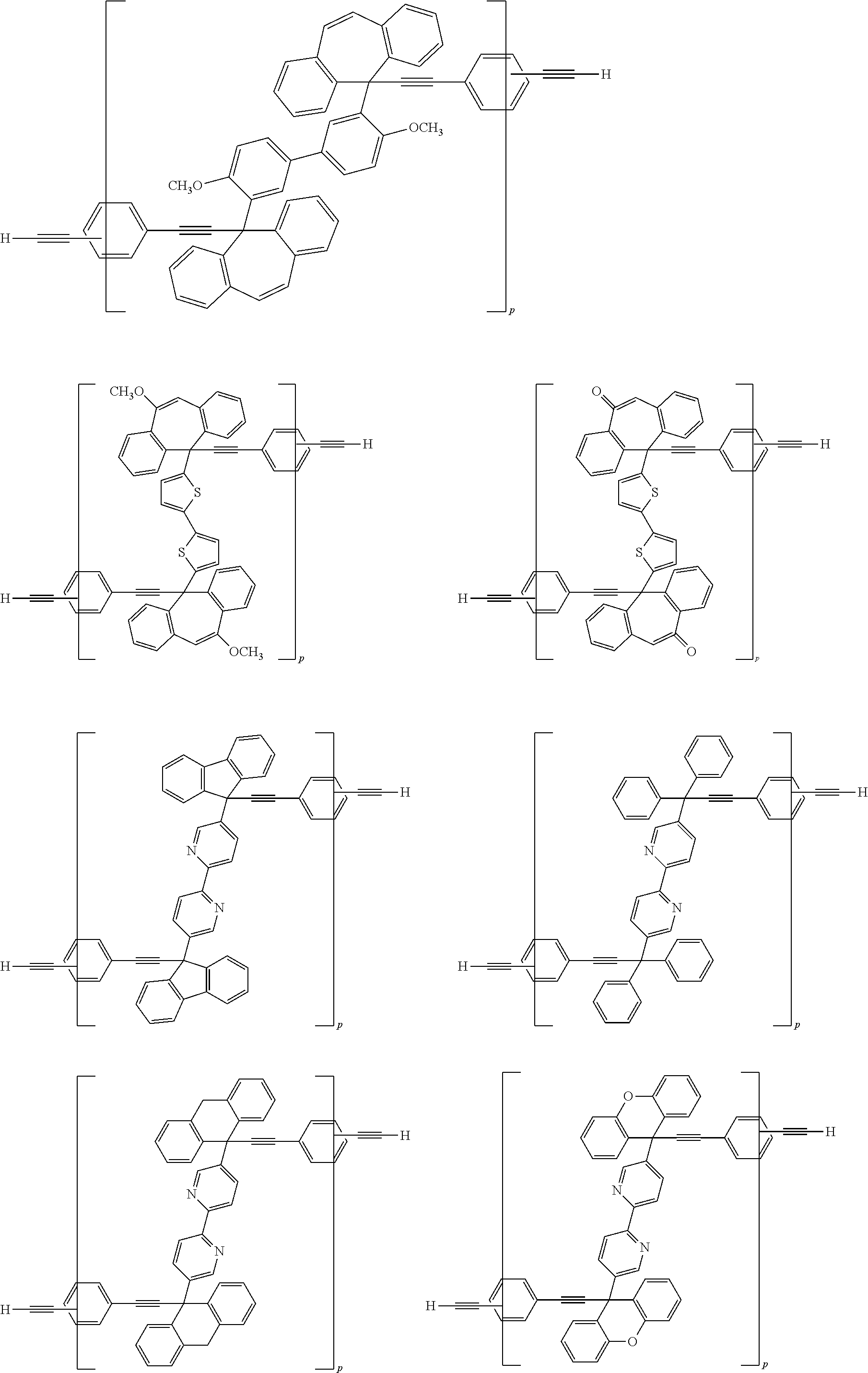


wherein Ar and Y have the same meanings as defined above; “n” is 2 or 3; M represents Li or Mg-Hal, and Hal represents Cl, Br, or I;

wherein Ar, Y, Hal, and “n” have the same meanings as defined above;

wherein Ar, Y, “n”, Hal, and R have the same meanings as defined above; and M1 represents Li or Mg-Hal.

wherein AR1, AR2, X, Y, “m”, and “n” have the same meanings as defined above; M represents Li or Mg-Hal, and Hal represents Cl, Br, or I;

wherein AR1, AR2, X, Y, “m”, “n”, and Hal have the same meanings as defined above;

wherein AR1, AR2, X, Y, Z, “m”, “n”, and Hal have the same meanings as defined above; M1 represents Li or Mg-Hal; “a” bonds with “b”, and “d” represents a hydrogen atom or bonds with “a”.

In this formula, AR1, AR2, X, Y, Z, “m”, “n”, and Hal have the same meanings as defined above; M1 represents Li or Mg-Hal; “a” bonds with “b”; “e” represents M1 or bonds with “a”; and “f” represents a monovalent organic group having 1 to 30 carbon atoms or bonds with “a”.


Biphenyl Derivative (B3):

Compound (A20)


Preparation of Organic Film Material (UDL-1 to 19, Comparative UDL-1 to 8)
| TABLE 1 | |||||
| Composition | Compound (1) | Compound (2) | Compound (3) | Compound (4) | PGMEA |
| for forming | (parts by | (parts by | (parts by | (parts by | (parts |
| organic film | mass) | mass) | mass) | mass) | by mass) |
| UDL-1 | A3 (5) | — | — | — | 100 |
| UDL-2 | A4 (5) | — | — | — | 100 |
| UDL-3 | A5 (5) | — | — | — | 100 |
| UDL-4 | A6 (5) | — | — | — | 100 |
| UDL-5 | A7 (5) | — | — | — | 100 |
| UDL-6 | A8 (5) | — | — | — | 100 |
| UDL-7 | A9 (5) | — | — | — | 100 |
| UDL-8 | A10 (5) | — | — | — | 100 |
| UDL-9 | A11 (5) | — | — | — | 100 |
| UDL-10 | A12 (5) | — | — | — | 100 |
| UDL-11 | A13 (5) | — | — | — | 100 |
| UDL-12 | A15 (5) | — | — | — | 100 |
| UDL-13 | A16 (5) | — | — | — | 100 |
| UDL-14 | A3 (5) | — | — | S1 (10) | 90 |
| UDL-15 | A3 (5) | — | — | S1 (10) | 90 |
| UDL-16 | A10 (5) | — | — | S1 (10) | 90 |
| UDL-17 | A10 (5) | — | — | S2 (10) | 90 |
| UDL-18 | A4 (3) | A18 (2) | — | — | 100 |
| UDL-19 | A4 (3) | A19 (2) | — | — | 100 |
| Comparative | A21 (5) | — | — | — | 100 |
| UDL-1 | |||||
| Comparative | A22 (5) | — | — | — | 100 |
| UDL-2 | |||||
| Comparative | A23 (5) | — | — | — | 100 |
| UDL-3 | |||||
| Comparative | A20 (5) | — | — | — | 100 |
| UDL-4 | |||||
| Comparative | B5 (5) | — | — | — | 100 |
| UDL-5 | |||||
| Comparative | A23 (5) | — | CR1 (1) | AG1 (0.05) | 100 |
| UDL-6 | |||||
| Comparative | A20 (5) | — | CR1 (1) | AG1 (0.05) | 100 |
| UDL-7 | |||||
| Comparative | B5 (5) | — | CR1 (1) | AG1 (0.05) | 100 |
| UDL-8 | |||||

| TABLE 2 | ||||
| Composition | Film thickness | Film thickness | b/a × | |
| for forming | after forming | after PGMEA | 100 | |
| organic film | film: a (Å) | treatment: b (Å) | (%) | |
| Example 1-1 | UDL-1 | 1153 | 1149 | 99.7 |
| Example 1-2 | UDL-2 | 1158 | 1158 | 100.0 |
| Example 1-3 | UDL-3 | 1152 | 1152 | 100.0 |
| Example 1-4 | UDL-4 | 1149 | 1149 | 100.0 |
| Example 1-5 | UDL-5 | 1153 | 1153 | 100.0 |
| Example 1-6 | UDL-6 | 1152 | 1151 | 99.9 |
| Example 1-7 | UDL-7 | 1146 | 1145 | 99.9 |
| Example 1-8 | UDL-8 | 1153 | 1152 | 99.9 |
| Example 1-9 | UDL-9 | 1155 | 1155 | 100.0 |
| Example 1-10 | UDL-10 | 1147 | 1146 | 99.9 |
| Example 1-11 | UDL-11 | 1150 | 1150 | 100.0 |
| Example 1-12 | UDL-12 | 1157 | 1156 | 99.9 |
| Example 1-13 | UDL-13 | 1150 | 1150 | 100.0 |
| Example 1-14 | UDL-14 | 1156 | 1146 | 99.1 |
| Example 1-15 | UDL-15 | 1154 | 1151 | 99.7 |
| Example 1-16 | UDL-16 | 1158 | 1150 | 99.3 |
| Example 1-17 | UDL-17 | 1159 | 1144 | 98.7 |
| Example 1-18 | UDL-18 | 1154 | 1153 | 99.9 |
| Example 1-19 | UDL-19 | 1152 | 1151 | 99.9 |
| Comparative | Comparative | 1148 | 1137 | 99.0 |
| Example 1-1 | UDL-1 | |||
| Comparative | Comparative | 1148 | 1140 | 99.3 |
| Example 1-2 | UDL-2 | |||
| Comparative | Comparative | 1154 | 444 | 38.5 |
| Example 1-3 | UDL-3 | |||
| Comparative | Comparative | 1155 | 252 | 21.8 |
| Example 1-4 | UDL-4 | |||
| Comparative | Comparative | 1141 | 240 | 21.0 |
| Example 1-5 | UDL-5 | |||
| Comparative | Comparative | 1153 | 1152 | 99.9 |
| Example 1-6 | UDL-6 | |||
| Comparative | Comparative | 1145 | 1140 | 99.6 |
| Example 1-7 | UDL-7 | |||
| Comparative | Comparative | 1150 | 1144 | 99.5 |
| Example 1-8 | UDL-8 | |||
| TABLE 3 | ||||
| Composition | Film thickness | Film thickness | b/a × | |
| for forming | after forming | after PGMEA | 100 | |
| organic film | film: a (Å) | treatment: b (Å) | (%) | |
| Example 2-1 | UDL-1 | 1152 | 1149 | 99.7 |
| Example 2-2 | UDL-2 | 1151 | 1149 | 99.8 |
| Example 2-3 | UDL-3 | 1148 | 1145 | 99.7 |
| Example 2-4 | UDL-4 | 1155 | 1154 | 99.9 |
| Example 2-5 | UDL-5 | 1155 | 1155 | 100.0 |
| Example 2-6 | UDL-6 | 1143 | 1142 | 99.9 |
| Example 2-7 | UDL-7 | 1157 | 1152 | 99.6 |
| Example 2-8 | UDL-8 | 1152 | 1150 | 99.8 |
| Example 2-9 | UDL-9 | 1146 | 1143 | 99.7 |
| Example 2-10 | UDL-10 | 1147 | 1143 | 99.7 |
| Example 2-11 | UDL-11 | 1157 | 1152 | 99.6 |
| Example 2-12 | UDL-12 | 1148 | 1144 | 99.7 |
| Example 2-13 | UDL-13 | 1146 | 1146 | 100.0 |
| Example 2-14 | UDL-14 | 1153 | 1152 | 99.9 |
| Example 2-15 | UDL-15 | 1152 | 1138 | 98.8 |
| Example 2-16 | UDL-16 | 1158 | 1152 | 99.5 |
| Example 2-17 | UDL-17 | 1155 | 1152 | 99.7 |
| Example 2-18 | UDL-18 | 1152 | 1146 | 99.5 |
| Example 2-19 | UDL-19 | 1150 | 1150 | 100.0 |
| Comparative | Comparative | 1157 | 1147 | 99.1 |
| Example 2-1 | UDL-1 | |||
| Comparative | Comparative | 1153 | 1143 | 99.1 |
| Example 2-2 | UDL-2 | |||
| Comparative | Comparative | 1146 | 1139 | 99.4 |
| Example 2-3 | UDL-3 | |||
| Comparative | Comparative | 1154 | 444 | 38.5 |
| Example 2-4 | UDL-4 | |||
| Comparative | Comparative | 1150 | 451 | 39.2 |
| Example 2-5 | UDL-5 | |||
| Comparative | Comparative | 1148 | 1138 | 99.1 |
| Example 2-6 | UDL-6 | |||
| Comparative | Comparative | 1156 | 1148 | 99.3 |
| Example 2-7 | UDL-7 | |||
| Comparative | Comparative | 1144 | 1138 | 99.5 |
| Example 2-8 | UDL-8 | |||
| TABLE 4 | ||||
| Film thickness | Film thickness | |||
| Composition | baked | baked | (B/A) × | |
| for forming | at 180° C.: | at 450° C.: | 100 | |
| organic film | A (Å) | B (Å) | (%) | |
| Example 3-1 | UDL-1 | 1153 | 1142 | 99.0 |
| Example 3-2 | UDL-2 | 1156 | 1156 | 100.0 |
| Example 3-3 | UDL-3 | 1152 | 1152 | 100.0 |
| Example 3-4 | UDL-4 | 1154 | 1154 | 100.0 |
| Example 3-5 | UDL-5 | 1155 | 1155 | 100.0 |
| Example 3-6 | UDL-6 | 1153 | 1145 | 99.3 |
| Example 3-7 | UDL-7 | 1146 | 1146 | 100.0 |
| Example 3-8 | UDL-8 | 1151 | 1145 | 99.5 |
| Example 3-9 | UDL-9 | 1147 | 1137 | 99.1 |
| Example 3-10 | UDL-10 | 1142 | 1135 | 99.4 |
| Example 3-11 | UDL-11 | 1155 | 1155 | 100.0 |
| Example 3-12 | UDL-12 | 1153 | 1143 | 99.2 |
| Example 3-13 | UDL-13 | 1152 | 1150 | 99.8 |
| Example 3-14 | UDL-14 | 1150 | 1147 | 99.7 |
| Example 3-15 | UDL-15 | 1153 | 1149 | 99.7 |
| Example 3-16 | UDL-16 | 1157 | 1146 | 99.0 |
| Example 3-17 | UDL-17 | 1157 | 1146 | 99.1 |
| Example 3-18 | UDL-18 | 1151 | 1150 | 99.9 |
| Example 3-19 | UDL-19 | 1151 | 1151 | 100.0 |
| Comparative | Comparative | 1154 | 1011 | 87.6 |
| Example 3-1 | UDL-1 | |||
| Comparative | Comparative | 1154 | 1017 | 88.1 |
| Example 3-2 | UDL-2 | |||
| Comparative | Comparative | 1155 | 274 | 23.7 |
| Example 3-3 | UDL-3 | |||
| Comparative | Comparative | 1150 | 246 | 21.4 |
| Example 3-4 | UDL-4 | |||
| Comparative | Comparative | 1153 | 264 | 22.9 |
| Example 3-5 | UDL-5 | |||
| Comparative | Comparative | 1157 | 1038 | 89.7 |
| Example 3-6 | UDL-6 | |||
| Comparative | Comparative | 1157 | 1026 | 88.7 |
| Example 3-7 | UDL-7 | |||
| Comparative | Comparative | 1154 | 1023 | 88.6 |
| Example 3-8 | UDL-8 | |||
| TABLE 5 | ||||
| Composition for | ||||
| forming organic film | Void | |||
| Example 4-1 | UDL-1 | Non | ||
| Example 4-2 | UDL-2 | Non | ||
| Example 4-3 | UDL-3 | Non | ||
| Example 4-4 | UDL-4 | Non | ||
| Example 4-5 | UDL-5 | Non | ||
| Example 4-6 | UDL-6 | Non | ||
| Example 4-7 | UDL-7 | Non | ||
| Example 4-8 | UDL-8 | Non | ||
| Example 4-9 | UDL-9 | Non | ||
| Example 4-10 | UDL-10 | Non | ||
| Example 4-11 | UDL-11 | Non | ||
| Example 4-12 | UDL-12 | Non | ||
| Example 4-13 | UDL-13 | Non | ||
| Example 4-14 | UDL-14 | Non | ||
| Example 4-15 | UDL-15 | Non | ||
| Example 4-16 | UDL-16 | Non | ||
| Example 4-17 | UDL-17 | Non | ||
| Example 4-18 | UDL-18 | Non | ||
| Example 4-19 | UDL-19 | Non | ||
| Comparative Example 4-1 | Comparative UDL-1 | Exist | ||
| Comparative Example 4-2 | Comparative UDL-2 | Exist | ||
| Comparative Example 4-3 | Comparative UDL-3 | Exist | ||
| Comparative Example 4-4 | Comparative UDL-4 | Exist | ||
| Comparative Example 4-5 | Comparative UDL-5 | Exist | ||
| Comparative Example 4-6 | Comparative UDL-6 | Exist | ||
| Comparative Example 4-7 | Comparative UDL-7 | Exist | ||
| Comparative Example 4-8 | Comparative UDL-8 | Exist | ||
| TABLE 6 | ||||
| Composition for | Step | |||
| forming organic film | (nm) | |||
| Example 5-1 | UDL-2 | 50 | ||
| Example 5-2 | UDL-3 | 40 | ||
| Example 5-3 | UDL-5 | 50 | ||
| Example 5-4 | UDL-6 | 50 | ||
| Example 5-5 | UDL-7 | 50 | ||
| Example 5-6 | UDL-8 | 40 | ||
| Example 5-7 | UDL-9 | 40 | ||
| Example 5-8 | UDL-10 | 45 | ||
| Example 5-9 | UDL-11 | 45 | ||
| Example 5-10 | UDL-12 | 40 | ||
| Example 5-11 | UDL-13 | 40 | ||
| Example 5-12 | UDL-16 | 25 | ||
| Example 5-13 | UDL-17 | 25 | ||
| Example 5-14 | UDL-18 | 45 | ||
| Example 5-15 | UDL-19 | 45 | ||
| Comparative Example 5-1 | Comparative UDL-1 | 90 | ||
| Comparative Example 5-2 | Comparative UDL-2 | 90 | ||
| Comparative Example 5-3 | Comparative UDL-3 | 90 | ||
| Comparative Example 5-4 | Comparative UDL-4 | 90 | ||
| Comparative Example 5-5 | Comparative UDL-5 | 85 | ||
| Comparative Example 5-6 | Comparative UDL-6 | 95 | ||
| Comparative Example 5-7 | Comparative UDL-7 | 95 | ||
| Comparative Example 5-8 | Comparative UDL-8 | 90 | ||
| TABLE 7 | ||||
| Polymer | Acid | Basic | Solvent | |
| (parts by | generator | compound | (parts by | |
| mass) | (parts by mass) | (parts by mass) | mass) | |
| Single layer | PR1 | PAG1 | Amine1 | PEGMEA |
| resist for ArF | (100) | (6.6) | (0.8) | (2500) |

| TABLE 8 | ||
| Polymer (parts by mass) | Organic solvent (parts by mass) | |
| TC-1 | PP1 (100) | diisoamyl ether | (2700) |
| 2-methyl-1-butanol | (270) | ||

- Chamber pressure 10.0 Pa
- RF power 1,500 W
- CF4 gas flow rate 75 sccm
- O2 gas flow rate 15 sccm
- Time 15 sec
Transcription conditions of the hard mask pattern to the organic film. - Chamber pressure 2.0 Pa
- RF power 500 W
- Ar gas flow rate 75 sccm
- O2 gas flow rate 45 sccm
- Time 120 sec
Transcription conditions of the organic film pattern to the SiO2 film. - Chamber pressure 2.0 Pa
- RF power 2,200 W
- C5F12 gas flow rate 20 sccm
- C2F6
gas flow rate 10 sccm - Ar gas flow rate 300 sccm
- O2 gas flow rate 60 sccm
- Time 90 sec
| TABLE 9 | ||
| Composition | Pattern profile after | |
| for forming | substrate | |
| organic film | transcription etching | |
| Example 6-1 | UDL-2 | Perpendicular |
| Example 6-2 | UDL-3 | Perpendicular |
| Example 6-3 | UDL-5 | Perpendicular |
| Example 6-4 | UDL-6 | Perpendicular |
| Example 6-5 | UDL-7 | Perpendicular |
| Example 6-6 | UDL-8 | Perpendicular |
| Example 6-7 | UDL-9 | Perpendicular |
| Example 6-8 | UDL-10 | Perpendicular |
| Example 6-9 | UDL-11 | Perpendicular |
| Example 6-10 | UDL-12 | Perpendicular |
| Example 6-11 | UDL-13 | Perpendicular |
| Example 6-12 | UDL-16 | Perpendicular |
| Example 6-13 | UDL-17 | Perpendicular |
| Example 6-14 | UDL-18 | Perpendicular |
| Example 6-15 | UDL-19 | Perpendicular |
| Comparative Example 6-1 | Comparative UDL-1 | Perpendicular |
| Comparative Example 6-2 | Comparative UDL-2 | Perpendicular |
| Comparative Example 6-3 | Comparative UDL-3 | Pattern collapse |
| Comparative Example 6-4 | Comparative UDL-4 | Pattern collapse |
| Comparative Example 6-5 | Comparative UDL-5 | Pattern collapse |
| Comparative Example 6-6 | Comparative UDL-6 | Perpendicular |
| Comparative Example 6-7 | Comparative UDL-7 | Perpendicular |
| Comparative Example 6-8 | Comparative UDL-8 | Perpendicular |
| TABLE 10 | ||
| Composition | Pattern profile after | |
| for forming | substrate | |
| organic film | transcription etching | |
| Example 7-1 | UDL-2 | Perpendicular |
| Example 7-2 | UDL-3 | Perpendicular |
| Example 7-3 | UDL-5 | Perpendicular |
| Example 7-4 | UDL-6 | Perpendicular |
| Example 7-5 | UDL-7 | Perpendicular |
| Example 7-6 | UDL-8 | Perpendicular |
| Example 7-7 | UDL-9 | Perpendicular |
| Example 7-8 | UDL-10 | Perpendicular |
| Example 7-9 | UDL-11 | Perpendicular |
| Example 7-10 | UDL-12 | Perpendicular |
| Example 7-11 | UDL-13 | Perpendicular |
| Example 7-12 | UDL-16 | Perpendicular |
| Example 7-13 | UDL-17 | Perpendicular |
| Example 7-14 | UDL-18 | Perpendicular |
| Example 7-15 | UDL-19 | Perpendicular |
| Comparative Example 7-1 | Comparative UDL-1 | Pattern collapse |
| Comparative Example 7-2 | Comparative UDL-2 | Pattern collapse |
| Comparative Example 7-3 | Comparative UDL-3 | Pattern collapse |
| Comparative Example 7-4 | Comparative UDL-4 | Pattern collapse |
| Comparative Example 7-5 | Comparative UDL-5 | Pattern collapse |
| Comparative Example 7-6 | Comparative UDL-6 | Pattern collapse |
| Comparative Example 7-7 | Comparative UDL-7 | Pattern collapse |
| Comparative Example 7-8 | Comparative UDL-8 | Pattern collapse |
Claims (13)


Priority Applications (7)
| Application Number | Priority Date | Filing Date | Title |
|---|---|---|---|
| US16/013,672 US10604618B2 (en) | 2018-06-20 | 2018-06-20 | Compound, method for manufacturing the compound, and composition for forming organic film |
| JP2019102009A JP2019218336A (en) | 2018-06-20 | 2019-05-31 | Compound, manufacturing method of compound, and composition for organic film formation |
| EP19178429.7A EP3584238B1 (en) | 2018-06-20 | 2019-06-05 | Compound, method for manufacturing the compound, and composition for forming organic film |
| TW108121170A TWI711599B (en) | 2018-06-20 | 2019-06-19 | Compound, method for manufacturing the compound, and composition for forming organic film |
| KR1020190073068A KR102361242B1 (en) | 2018-06-20 | 2019-06-19 | Compound, method for manufacturing the compound, and composition for forming organic film |
| CN201910539260.9A CN110627600B (en) | 2018-06-20 | 2019-06-20 | Compound, method for producing compound, and composition for forming organic film |
| JP2023125533A JP2023162189A (en) | 2018-06-20 | 2023-08-01 | Compound and organic film-forming composition |
Applications Claiming Priority (1)
| Application Number | Priority Date | Filing Date | Title |
|---|---|---|---|
| US16/013,672 US10604618B2 (en) | 2018-06-20 | 2018-06-20 | Compound, method for manufacturing the compound, and composition for forming organic film |
Publications (2)
| Publication Number | Publication Date |
|---|---|
| US20190390000A1 US20190390000A1 (en) | 2019-12-26 |
| US10604618B2 true US10604618B2 (en) | 2020-03-31 |
Family
ID=66770346
Family Applications (1)
| Application Number | Title | Priority Date | Filing Date |
|---|---|---|---|
| US16/013,672 Active US10604618B2 (en) | 2018-06-20 | 2018-06-20 | Compound, method for manufacturing the compound, and composition for forming organic film |
Country Status (6)
| Country | Link |
|---|---|
| US (1) | US10604618B2 (en) |
| EP (1) | EP3584238B1 (en) |
| JP (2) | JP2019218336A (en) |
| KR (1) | KR102361242B1 (en) |
| CN (1) | CN110627600B (en) |
| TW (1) | TWI711599B (en) |
Cited By (1)
| Publication number | Priority date | Publication date | Assignee | Title |
|---|---|---|---|---|
| US11307497B2 (en) * | 2018-03-28 | 2022-04-19 | Shin-Etsu Chemical Co., Ltd. | Compound, composition for forming organic film, substrate for manufacturing semiconductor apparatus, method for forming organic film, and patterning process |
Families Citing this family (9)
| Publication number | Priority date | Publication date | Assignee | Title |
|---|---|---|---|---|
| US11022882B2 (en) * | 2018-06-20 | 2021-06-01 | Shin-Etsu Chemical Co., Ltd. | Compound and composition for forming organic film |
| US20200142309A1 (en) * | 2018-11-02 | 2020-05-07 | Rohm And Haas Electronic Materials Llc | Aromatic underlayer |
| JP7161451B2 (en) * | 2019-07-05 | 2022-10-26 | 信越化学工業株式会社 | Composition for forming organic film, substrate for manufacturing semiconductor device, method for forming organic film, and method for forming pattern |
| JP7368322B2 (en) * | 2020-06-12 | 2023-10-24 | 信越化学工業株式会社 | Resist underlayer film material, pattern forming method, and resist underlayer film forming method |
| JP2022124133A (en) * | 2021-02-15 | 2022-08-25 | 信越化学工業株式会社 | Material for forming organic film, substrate for manufacturing semiconductor device, method for forming organic film, patterning process, and compound for forming organic film |
| KR20220125770A (en) * | 2021-03-05 | 2022-09-14 | 엘티소재주식회사 | Heterocyclic compound, organic light emitting device comprising the same, manufacturing method of the same and composition for organic layer of organic light emitting device |
| KR20230029051A (en) * | 2021-08-23 | 2023-03-03 | 삼성에스디아이 주식회사 | Hardmask composition, hardmask layer and method of forming patterns |
| JP2023077955A (en) * | 2021-11-25 | 2023-06-06 | 信越化学工業株式会社 | Material for forming organic film, substrate for manufacturing semiconductor device, method for forming organic film, and patterning process |
| CN116514752B (en) * | 2023-06-27 | 2023-12-01 | 吉林奥来德光电材料股份有限公司 | Light-emitting auxiliary material, preparation method and application thereof in organic electroluminescent device |
Citations (23)
| Publication number | Priority date | Publication date | Assignee | Title |
|---|---|---|---|---|
| US20020106909A1 (en) | 2001-02-07 | 2002-08-08 | Hitoshi Kato | Silicon nitride film forming method, silicon nitride film forming system and silicon nitride film forming system precleaning method |
| JP2002334869A (en) | 2001-02-07 | 2002-11-22 | Tokyo Electron Ltd | Method and device for forming silicon nitride film, and method for preprocessing of cleaning thereof |
| WO2004066377A1 (en) | 2003-01-24 | 2004-08-05 | Tokyo Electron Limited | Method of cvd for forming silicon nitride film on substrate |
| JP2005128509A (en) | 2003-10-03 | 2005-05-19 | Shin Etsu Chem Co Ltd | Material for forming photoresist lower layer film and method for forming pattern |
| US20060019195A1 (en) | 2003-10-03 | 2006-01-26 | Jun Hatakeyama | Photoresist undercoat-forming material and patterning process |
| US20060204891A1 (en) | 2005-03-11 | 2006-09-14 | Shin-Etsu Chemical Co., Ltd. | Photoresist undercoat-forming material and patterning process |
| JP2006285095A (en) | 2005-04-04 | 2006-10-19 | Shin Etsu Chem Co Ltd | Resist lower layer film material and pattern forming method |
| JP2006293298A (en) | 2005-03-11 | 2006-10-26 | Shin Etsu Chem Co Ltd | Photoresist undercoat-forming material and patterning process |
| JP2007199653A (en) | 2005-12-27 | 2007-08-09 | Shin Etsu Chem Co Ltd | Photoresist underlayer film forming material and pattern forming method |
| KR100874655B1 (en) | 2007-07-20 | 2008-12-17 | 금호석유화학 주식회사 | Polymer for spin on carbon hardmask and preparation method thereof, spin on carbon hardmask composition containing the polymer and patterning method of semiconductor device using the composition |
| US20090274978A1 (en) | 2008-05-01 | 2009-11-05 | Masaki Ohashi | Novel photoacid generator, resist composition, and patterning process |
| US20100099044A1 (en) | 2008-10-20 | 2010-04-22 | Shin-Etsu Chemical Co.,Ltd. | Method for forming resist underlayer film, patterning process using the same, and composition for the resist underlayer film |
| JP2010181605A (en) | 2009-02-05 | 2010-08-19 | Jsr Corp | Composition for forming resist underfilm, resist underfilm, method for forming the resist underfilm, and method for forming pattern |
| JP2012215842A (en) | 2011-03-31 | 2012-11-08 | Jsr Corp | Composition for forming resist underlay film and pattern forming method |
| US20130302990A1 (en) | 2012-05-08 | 2013-11-14 | Shin-Etsu Chemical Co., Ltd. | Organic film composition, method for forming organic film and patterning process using this, and heat-decomposable polymer |
| US8765899B2 (en) | 2007-11-06 | 2014-07-01 | Braggone Oy | Carbosilane polymer compositions for anti-reflective coatings |
| WO2014208324A1 (en) | 2013-06-24 | 2014-12-31 | Jsr株式会社 | Composition for film formation use, resist underlayer film and method for formation thereof, pattern formation method, and compound |
| US9018776B2 (en) | 2010-12-16 | 2015-04-28 | Cheil Industries, Inc. | Hardmask composition including aromatic ring-containing compound, method of forming patterns, and semiconductor integrated circuit device including the patterns |
| US9261788B2 (en) | 2012-06-18 | 2016-02-16 | Shin-Etsu Chemical Co., Ltd. | Compound for forming organic film, and organic film composition using the same, process for forming organic film, and patterning process |
| JP2016044272A (en) | 2014-08-25 | 2016-04-04 | Jsr株式会社 | Composition for forming film, film and manufacturing method and compound of substrate having formed pattern |
| JP2016060886A (en) | 2014-09-19 | 2016-04-25 | Jsr株式会社 | Composition for forming film, film, method for manufacturing patterned substrate, and compound |
| US9328246B2 (en) | 2012-01-19 | 2016-05-03 | Brewer Science Inc. | Nonpolymeric antireflection compositions containing adamantyl groups |
| US20170184968A1 (en) | 2015-12-24 | 2017-06-29 | Shin-Etsu Chemical Co., Ltd. | Compound for forming organic film, composition for forming organic film, method for forming organic film, and patterning process |
Family Cites Families (5)
| Publication number | Priority date | Publication date | Assignee | Title |
|---|---|---|---|---|
| WO2001009117A1 (en) * | 1999-07-29 | 2001-02-08 | Allellix Neuroscience Inc. | Tricyclic compounds as glycine transport inhibitors |
| JP5385006B2 (en) * | 2009-05-25 | 2014-01-08 | 信越化学工業株式会社 | Resist underlayer film material and pattern forming method using the same |
| JP6319059B2 (en) * | 2014-11-25 | 2018-05-09 | 信越化学工業株式会社 | Photomask blank, resist pattern forming method, and photomask manufacturing method |
| JP6625934B2 (en) * | 2015-07-14 | 2019-12-25 | 信越化学工業株式会社 | Resist underlayer film material, pattern forming method, and compound |
| KR102452808B1 (en) * | 2016-06-16 | 2022-10-07 | 동우 화인켐 주식회사 | Composition for hard mask |
-
2018
- 2018-06-20 US US16/013,672 patent/US10604618B2/en active Active
-
2019
- 2019-05-31 JP JP2019102009A patent/JP2019218336A/en active Pending
- 2019-06-05 EP EP19178429.7A patent/EP3584238B1/en active Active
- 2019-06-19 TW TW108121170A patent/TWI711599B/en active
- 2019-06-19 KR KR1020190073068A patent/KR102361242B1/en active IP Right Grant
- 2019-06-20 CN CN201910539260.9A patent/CN110627600B/en active Active
-
2023
- 2023-08-01 JP JP2023125533A patent/JP2023162189A/en active Pending
Patent Citations (30)
| Publication number | Priority date | Publication date | Assignee | Title |
|---|---|---|---|---|
| US20020106909A1 (en) | 2001-02-07 | 2002-08-08 | Hitoshi Kato | Silicon nitride film forming method, silicon nitride film forming system and silicon nitride film forming system precleaning method |
| JP2002334869A (en) | 2001-02-07 | 2002-11-22 | Tokyo Electron Ltd | Method and device for forming silicon nitride film, and method for preprocessing of cleaning thereof |
| WO2004066377A1 (en) | 2003-01-24 | 2004-08-05 | Tokyo Electron Limited | Method of cvd for forming silicon nitride film on substrate |
| US20050255712A1 (en) | 2003-01-24 | 2005-11-17 | Tokyo Electronlimited | Method of cvd for forming silicon nitride film on substrate |
| JP2005128509A (en) | 2003-10-03 | 2005-05-19 | Shin Etsu Chem Co Ltd | Material for forming photoresist lower layer film and method for forming pattern |
| US20060019195A1 (en) | 2003-10-03 | 2006-01-26 | Jun Hatakeyama | Photoresist undercoat-forming material and patterning process |
| US20060204891A1 (en) | 2005-03-11 | 2006-09-14 | Shin-Etsu Chemical Co., Ltd. | Photoresist undercoat-forming material and patterning process |
| JP2006293298A (en) | 2005-03-11 | 2006-10-26 | Shin Etsu Chem Co Ltd | Photoresist undercoat-forming material and patterning process |
| JP2006285095A (en) | 2005-04-04 | 2006-10-19 | Shin Etsu Chem Co Ltd | Resist lower layer film material and pattern forming method |
| JP2007199653A (en) | 2005-12-27 | 2007-08-09 | Shin Etsu Chem Co Ltd | Photoresist underlayer film forming material and pattern forming method |
| KR100874655B1 (en) | 2007-07-20 | 2008-12-17 | 금호석유화학 주식회사 | Polymer for spin on carbon hardmask and preparation method thereof, spin on carbon hardmask composition containing the polymer and patterning method of semiconductor device using the composition |
| US8765899B2 (en) | 2007-11-06 | 2014-07-01 | Braggone Oy | Carbosilane polymer compositions for anti-reflective coatings |
| US20090274978A1 (en) | 2008-05-01 | 2009-11-05 | Masaki Ohashi | Novel photoacid generator, resist composition, and patterning process |
| JP2009269953A (en) | 2008-05-01 | 2009-11-19 | Shin Etsu Chem Co Ltd | New photoacid generator, resist material using the same, and pattern forming method |
| JP2010122656A (en) | 2008-10-20 | 2010-06-03 | Shin-Etsu Chemical Co Ltd | Method for forming resist underlayer film, patterning process using the same, and resist underlayer film material |
| US20100099044A1 (en) | 2008-10-20 | 2010-04-22 | Shin-Etsu Chemical Co.,Ltd. | Method for forming resist underlayer film, patterning process using the same, and composition for the resist underlayer film |
| JP2010181605A (en) | 2009-02-05 | 2010-08-19 | Jsr Corp | Composition for forming resist underfilm, resist underfilm, method for forming the resist underfilm, and method for forming pattern |
| US9018776B2 (en) | 2010-12-16 | 2015-04-28 | Cheil Industries, Inc. | Hardmask composition including aromatic ring-containing compound, method of forming patterns, and semiconductor integrated circuit device including the patterns |
| JP2012215842A (en) | 2011-03-31 | 2012-11-08 | Jsr Corp | Composition for forming resist underlay film and pattern forming method |
| US20130310514A1 (en) | 2011-03-31 | 2013-11-21 | Jsr Corporation | Resist underlayer film-forming composition |
| US9328246B2 (en) | 2012-01-19 | 2016-05-03 | Brewer Science Inc. | Nonpolymeric antireflection compositions containing adamantyl groups |
| US20130302990A1 (en) | 2012-05-08 | 2013-11-14 | Shin-Etsu Chemical Co., Ltd. | Organic film composition, method for forming organic film and patterning process using this, and heat-decomposable polymer |
| JP2013253227A (en) | 2012-05-08 | 2013-12-19 | Shin-Etsu Chemical Co Ltd | Organic film material, method for forming organic film and method for forming pattern using the same, and heat-decomposable polymer |
| US9261788B2 (en) | 2012-06-18 | 2016-02-16 | Shin-Etsu Chemical Co., Ltd. | Compound for forming organic film, and organic film composition using the same, process for forming organic film, and patterning process |
| WO2014208324A1 (en) | 2013-06-24 | 2014-12-31 | Jsr株式会社 | Composition for film formation use, resist underlayer film and method for formation thereof, pattern formation method, and compound |
| US20160085152A1 (en) | 2013-06-24 | 2016-03-24 | Jsr Corporation | Composition for film formation, resist underlayer film and forming method thereof, pattern-forming method and compound |
| JP2016044272A (en) | 2014-08-25 | 2016-04-04 | Jsr株式会社 | Composition for forming film, film and manufacturing method and compound of substrate having formed pattern |
| JP2016060886A (en) | 2014-09-19 | 2016-04-25 | Jsr株式会社 | Composition for forming film, film, method for manufacturing patterned substrate, and compound |
| US20170184968A1 (en) | 2015-12-24 | 2017-06-29 | Shin-Etsu Chemical Co., Ltd. | Compound for forming organic film, composition for forming organic film, method for forming organic film, and patterning process |
| JP2017119671A (en) | 2015-12-24 | 2017-07-06 | 信越化学工業株式会社 | Compound for forming organic film, composition for forming organic film, method for forming organic film, and patterning process |
Non-Patent Citations (6)
| Title |
|---|
| Apr. 20, 2018 Search Report. |
| Jiménez-Urias, Ana, et al., "Synthesis and Characterization of Dumbbell-Like BTD-Based Derivatives to Engineer Organic Building Blocks in Solid-State", Journal of Molecular Structure, vol. 1153, pp. 34-41. |
| Melissa Hughs, Miguel Jimenez, Saeed Khan, and Miguel A. Garcia-Garibay, Synthesis, Rotational Dynamics, and Photophysical Characterization of a Crystalline Linearly Conjugated Phenyleneethynylene Molecular Dirotor,3 | J. Org. Chem. 2013, 78, 5293-5302. (Year: 2013). * |
| Oral, Pavlo O., et al., "Semiempirical UNO-CAS and UNO-CI: Method and Applications in Nonoelectrics", The Journal of Physical Chemistry, vol. 115, No. 41, pp. 11303-11312. |
| Sep. 27, 2019 Extended European Search Report issued in European Patent Application No. 19178429.7. |
| Tommasini, Matteo, et al., "π-Conjugation and End Group Effects in Long Cumulenes: Raman Spectroscopy and OFT Calculations", The Journal of Physical Chemistry, vol. 118, No. 45, pp. 26415-26425. |
Cited By (1)
| Publication number | Priority date | Publication date | Assignee | Title |
|---|---|---|---|---|
| US11307497B2 (en) * | 2018-03-28 | 2022-04-19 | Shin-Etsu Chemical Co., Ltd. | Compound, composition for forming organic film, substrate for manufacturing semiconductor apparatus, method for forming organic film, and patterning process |
Also Published As
| Publication number | Publication date |
|---|---|
| JP2019218336A (en) | 2019-12-26 |
| JP2023162189A (en) | 2023-11-08 |
| CN110627600B (en) | 2022-07-01 |
| CN110627600A (en) | 2019-12-31 |
| EP3584238A1 (en) | 2019-12-25 |
| TWI711599B (en) | 2020-12-01 |
| EP3584238B1 (en) | 2023-01-18 |
| US20190390000A1 (en) | 2019-12-26 |
| KR102361242B1 (en) | 2022-02-09 |
| KR20190143410A (en) | 2019-12-30 |
| TW202000631A (en) | 2020-01-01 |
Similar Documents
| Publication | Publication Date | Title |
|---|---|---|
| US10604618B2 (en) | Compound, method for manufacturing the compound, and composition for forming organic film | |
| US11181821B2 (en) | Composition for forming organic film, substrate for manufacturing semiconductor apparatus, method for forming organic film, patterning process, and polymer | |
| US10998197B2 (en) | Polymer and composition for forming organic film, substrate for manufacturing semiconductor apparatus, method for forming organic film, and patterning process | |
| US11307497B2 (en) | Compound, composition for forming organic film, substrate for manufacturing semiconductor apparatus, method for forming organic film, and patterning process | |
| EP3584240B1 (en) | Compound and composition for forming organic film | |
| TWI751525B (en) | Material for forming organic film, substrate for manufacturing semiconductor device, method for forming organic film, patterning process, and compound for forming organic film | |
| CN104710588A (en) | Aromatic resins for underlayers | |
| US11635691B2 (en) | Composition for forming organic film, substrate for manufacturing semiconductor device, method for forming organic film, patterning process, and polymer | |
| TW202323241A (en) | Composition for forming organic film, patterning process, and compound and polymer for forming organic film | |
| US20230161258A1 (en) | Material for forming organic film, substrate for manufacturing semiconductor device, method for forming organic film, and patterning process | |
| TWI827359B (en) | Composition for forming organic film, patterning process, and compound and polymer for forming organic film | |
| US20220269175A1 (en) | Material for forming organic film, substrate for manufacturing semiconductor device, method for forming organic film, patterning process, and compound for forming organic film |
Legal Events
| Date | Code | Title | Description |
|---|---|---|---|
| AS | Assignment |
Owner name: SHIN-ETSU CHEMICAL CO., LTD., JAPAN Free format text: ASSIGNMENT OF ASSIGNORS INTEREST;ASSIGNORS:TACHIBANA, SEIICHIRO;WATANABE, TAKERU;NIIDA, KEISUKE;AND OTHERS;SIGNING DATES FROM 20180518 TO 20180521;REEL/FRAME:046149/0265 Owner name: INTERNATIONAL BUSINESS MACHINES CORPORATION, UNITE Free format text: ASSIGNMENT OF ASSIGNORS INTEREST;ASSIGNORS:HESS, ALEXANDER EDWARD;BREYTA, GREGORY;SANDERS, DANIEL PAUL;AND OTHERS;SIGNING DATES FROM 20180611 TO 20180614;REEL/FRAME:046149/0205 Owner name: INTERNATIONAL BUSINESS MACHINES CORPORATION, UNITED STATES Free format text: ASSIGNMENT OF ASSIGNORS INTEREST;ASSIGNORS:HESS, ALEXANDER EDWARD;BREYTA, GREGORY;SANDERS, DANIEL PAUL;AND OTHERS;SIGNING DATES FROM 20180611 TO 20180614;REEL/FRAME:046149/0205 |
|
| FEPP | Fee payment procedure |
Free format text: ENTITY STATUS SET TO UNDISCOUNTED (ORIGINAL EVENT CODE: BIG.); ENTITY STATUS OF PATENT OWNER: LARGE ENTITY |
|
| STPP | Information on status: patent application and granting procedure in general |
Free format text: NOTICE OF ALLOWANCE MAILED -- APPLICATION RECEIVED IN OFFICE OF PUBLICATIONS |
|
| STPP | Information on status: patent application and granting procedure in general |
Free format text: PUBLICATIONS -- ISSUE FEE PAYMENT VERIFIED |
|
| STCF | Information on status: patent grant |
Free format text: PATENTED CASE |
|
| MAFP | Maintenance fee payment |
Free format text: PAYMENT OF MAINTENANCE FEE, 4TH YEAR, LARGE ENTITY (ORIGINAL EVENT CODE: M1551); ENTITY STATUS OF PATENT OWNER: LARGE ENTITY Year of fee payment: 4 |