JP4380418B2 - 半導体装置の製造方法 - Google Patents
半導体装置の製造方法 Download PDFInfo
- Publication number
- JP4380418B2 JP4380418B2 JP2004157414A JP2004157414A JP4380418B2 JP 4380418 B2 JP4380418 B2 JP 4380418B2 JP 2004157414 A JP2004157414 A JP 2004157414A JP 2004157414 A JP2004157414 A JP 2004157414A JP 4380418 B2 JP4380418 B2 JP 4380418B2
- Authority
- JP
- Japan
- Prior art keywords
- impurity
- diffusion
- manufacturing
- silicon
- semiconductor device
- Prior art date
- Legal status (The legal status is an assumption and is not a legal conclusion. Google has not performed a legal analysis and makes no representation as to the accuracy of the status listed.)
- Expired - Lifetime
Links
Images


Landscapes
- Bipolar Transistors (AREA)
Description
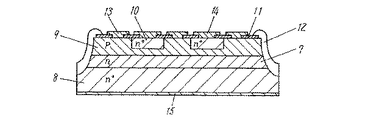
2 ボロン添加シリコン粉末
3 弗化アルミニウム
4 ノンドープシリコン粉末
5 石英管
6 金属アルミニウム
7 n型半導体領域(コレクタ領域)
8 n+型半導体領域(コレクタ領域)
9 p型半導体領域(ベース領域)
10 n+型半導体領域(エミッタ領域)
11 二酸化珪素
12 ガラス保護膜
13 ベース電極
14 エミッタ電極
15 コレクタ電極
Claims (2)
- 石英管内に半導体基板と不純物拡散源を設置する工程と、前記石英管を真空封入し、熱処理を行って前記半導体基板に不純物を導入する工程を備えた半導体装置の製造方法であって、前記拡散源は、第1の不純物を含む物質と第2の不純物を含む物質とを有し、前記第1の不純物を含む物質は前記第1の不純物を含まない物質で包むように構成され、前記第1の不純物を含む物質は弗化アルミニウム粉末であり、前記第2の不純物を含む物質はボロンを添加したシリコン粉末であり、前記不純物を含まない物質はノンドープシリコン粉末であることを特徴とする半導体装置の製造方法。
- 前記半導体基板に前記第1の不純物および前記第2の不純物が導入された領域はトランジスタのベース領域として機能することを特徴とする請求項1記載の半導体装置の製造方法。
Priority Applications (1)
| Application Number | Priority Date | Filing Date | Title |
|---|---|---|---|
| JP2004157414A JP4380418B2 (ja) | 2004-05-27 | 2004-05-27 | 半導体装置の製造方法 |
Applications Claiming Priority (1)
| Application Number | Priority Date | Filing Date | Title |
|---|---|---|---|
| JP2004157414A JP4380418B2 (ja) | 2004-05-27 | 2004-05-27 | 半導体装置の製造方法 |
Publications (2)
| Publication Number | Publication Date |
|---|---|
| JP2005340503A JP2005340503A (ja) | 2005-12-08 |
| JP4380418B2 true JP4380418B2 (ja) | 2009-12-09 |
Family
ID=35493719
Family Applications (1)
| Application Number | Title | Priority Date | Filing Date |
|---|---|---|---|
| JP2004157414A Expired - Lifetime JP4380418B2 (ja) | 2004-05-27 | 2004-05-27 | 半導体装置の製造方法 |
Country Status (1)
| Country | Link |
|---|---|
| JP (1) | JP4380418B2 (ja) |
Families Citing this family (1)
| Publication number | Priority date | Publication date | Assignee | Title |
|---|---|---|---|---|
| CN109616512A (zh) * | 2018-12-26 | 2019-04-12 | 瑞能半导体有限公司 | 半导体器件及其制造方法 |
-
2004
- 2004-05-27 JP JP2004157414A patent/JP4380418B2/ja not_active Expired - Lifetime
Also Published As
| Publication number | Publication date |
|---|---|
| JP2005340503A (ja) | 2005-12-08 |
Similar Documents
| Publication | Publication Date | Title |
|---|---|---|
| JP4380418B2 (ja) | 半導体装置の製造方法 | |
| JP3077760B2 (ja) | 固相拡散方法 | |
| JPH06112146A (ja) | 拡散型シリコン素子基板の製造方法 | |
| JP3144891B2 (ja) | 不純物拡散方法 | |
| JP3584544B2 (ja) | 半導体装置の製造方法 | |
| JPH03163821A (ja) | 半導体装置の製造方法 | |
| JP2973958B2 (ja) | 半導体装置の製造方法 | |
| JP2001110807A (ja) | 薄膜絶縁膜の形成方法 | |
| JPS5850411B2 (ja) | 不純物拡散法 | |
| JPS60175417A (ja) | 半導体装置の製造方法 | |
| JP3272908B2 (ja) | 半導体多層材料の製造方法 | |
| JPS609118A (ja) | 半導体装置の製造方法 | |
| JPS58130567A (ja) | 半導体装置の製造方法 | |
| JPS59225566A (ja) | 半導体素子の製造方法 | |
| JPS5927524A (ja) | 半導体装置の製造方法 | |
| JPH07335584A (ja) | シリコン基板へのアルミニウム拡散方法 | |
| JPS5939901B2 (ja) | 半導体装置の製造方法 | |
| JPS61294855A (ja) | 半導体装置の製造方法 | |
| JPS622530A (ja) | 半導体基板への不純物熱拡散方法 | |
| JPS5969923A (ja) | ほう素拡散方法 | |
| JPS5927106B2 (ja) | 半導体装置の製造方法 | |
| JPH04168764A (ja) | 半導体装置の製造方法 | |
| JPS5830735B2 (ja) | ハンドウタイソウチノ セイゾウホウホウ | |
| JPH0464227A (ja) | 半導体素子とその製造方法 | |
| JPH01282870A (ja) | 半導体装置の製造方法 |
Legal Events
| Date | Code | Title | Description |
|---|---|---|---|
| A621 | Written request for application examination |
Free format text: JAPANESE INTERMEDIATE CODE: A621 Effective date: 20070528 |
|
| RD01 | Notification of change of attorney |
Free format text: JAPANESE INTERMEDIATE CODE: A7421 Effective date: 20070613 |
|
| A131 | Notification of reasons for refusal |
Free format text: JAPANESE INTERMEDIATE CODE: A131 Effective date: 20090630 |
|
| A977 | Report on retrieval |
Free format text: JAPANESE INTERMEDIATE CODE: A971007 Effective date: 20090630 |
|
| A521 | Request for written amendment filed |
Free format text: JAPANESE INTERMEDIATE CODE: A523 Effective date: 20090806 |
|
| TRDD | Decision of grant or rejection written | ||
| A01 | Written decision to grant a patent or to grant a registration (utility model) |
Free format text: JAPANESE INTERMEDIATE CODE: A01 Effective date: 20090901 |
|
| A01 | Written decision to grant a patent or to grant a registration (utility model) |
Free format text: JAPANESE INTERMEDIATE CODE: A01 |
|
| A61 | First payment of annual fees (during grant procedure) |
Free format text: JAPANESE INTERMEDIATE CODE: A61 Effective date: 20090914 |
|
| FPAY | Renewal fee payment (event date is renewal date of database) |
Free format text: PAYMENT UNTIL: 20121002 Year of fee payment: 3 |
|
| FPAY | Renewal fee payment (event date is renewal date of database) |
Free format text: PAYMENT UNTIL: 20121002 Year of fee payment: 3 |