JP4380418B2 - Manufacturing method of semiconductor device - Google Patents
Manufacturing method of semiconductor device Download PDFInfo
- Publication number
- JP4380418B2 JP4380418B2 JP2004157414A JP2004157414A JP4380418B2 JP 4380418 B2 JP4380418 B2 JP 4380418B2 JP 2004157414 A JP2004157414 A JP 2004157414A JP 2004157414 A JP2004157414 A JP 2004157414A JP 4380418 B2 JP4380418 B2 JP 4380418B2
- Authority
- JP
- Japan
- Prior art keywords
- impurity
- diffusion
- manufacturing
- silicon
- semiconductor device
- Prior art date
- Legal status (The legal status is an assumption and is not a legal conclusion. Google has not performed a legal analysis and makes no representation as to the accuracy of the status listed.)
- Active
Links
Images


Description
本発明は、シリコン基板中へ二種の不純物を同時に再現性よく拡散させるのに適した半導体装置の製造方法に関するものである。 The present invention relates to a method for manufacturing a semiconductor device suitable for simultaneously diffusing two kinds of impurities into a silicon substrate with good reproducibility.
従来、シリコン基板に二種の不純物を拡散させる方法として、石英封管拡散法が広く知られている(例えば特許文献1参照)。 Conventionally, a quartz sealed tube diffusion method is widely known as a method for diffusing two types of impurities in a silicon substrate (see, for example, Patent Document 1).
石英封管拡散法には、例えば、拡散不純物として、シリコン粉末に固溶した元素と単体金属の二種の不純物を用いて、同時にシリコン基板に拡散する封管拡散法技術がある。この技術は、シリコン粉末に固溶した元素と単体金属の二種の不純物を封管内に入れた後、熱処理することによって、シリコン基板の片面に二種の不純物を拡散するものである。 The quartz sealed tube diffusion method includes, for example, a sealed tube diffusion technique in which two types of impurities, a solid solution element in silicon powder and a single metal, are used as diffusion impurities and simultaneously diffused into a silicon substrate. In this technique, two kinds of impurities, an element dissolved in silicon powder and a single metal, are put in a sealed tube and then heat-treated to diffuse the two kinds of impurities on one side of the silicon substrate.
図4は従来の技術における石英管による封管拡散法の説明図である。 FIG. 4 is an explanatory diagram of a sealed tube diffusion method using a quartz tube in the prior art.
シリコン基板1を300sl並べ、その両側に拡散源となるボロン添加シリコン粉末2、金属アルミニウム6を配置し、さらに基板間にも100sl間隔で配置する。この後、石英管5内を真空封止し、1200℃で9時間熱拡散を行う。しかるのち、シリコン基板1を取り出し再度1200℃で50時間ドライブイン拡散を行う。
また、同じく特許文献1には次に示す別の技術も開示されている。この技術は拡散不純物として、シリコン粉末に固溶した元素とハロゲン化物の二種を封管内に入れた後、熱処理することによって、シリコン基板の片面に二種の不純物を拡散することができるとされている。
Similarly,
図5は従来の別の技術における石英管による封管拡散法の説明図である。 FIG. 5 is an explanatory view of a sealed tube diffusion method using a quartz tube in another conventional technique.
シリコン基板1を300sl並べ、その両側に拡散源となるボロン添加シリコン粉末2、弗化アルミニウム3を配置し、さらに基板間にも100sl間隔で配置する。この後、石英管5内を真空封止し、1200℃で9時間熱拡散を行う。しかるのち、シリコン基板1を取り出し再度1200℃で50時間ドライブイン拡散を行う。
上記の従来技術のように単に単体金属を用いるのではなく、ハロゲン化物を用いることで、金属元素の蒸気圧よりも高い蒸気圧となり、封管内での濃度差を少なくし、拡散深さのばらつきを少なくすることができるとされている。
上記した封管内に単体金属を封入する方法では、シリコン粉末に固溶した元素として、シリコン中にリンもしくはボロンを添加させた粉末が用いられ、単体金属としてはアルミニウムもしくはガリウムが用いられることが多い。しかしながら、金属のアルミニウムもしくはガリウムの蒸気圧は低いため、封管内に金属元素を配置し、熱処理した場合、蒸発が進まず封管内で濃度差を生じ、その結果、アルミニウムもしくはガリウムの拡散深さ、拡散長にばらつきを生じやすいという問題があった。 In the above-described method of enclosing a single metal in a sealed tube, a powder obtained by adding phosphorus or boron into silicon is used as an element dissolved in silicon powder, and aluminum or gallium is often used as the single metal. . However, since the vapor pressure of the metal aluminum or gallium is low, when a metal element is placed in the sealed tube and heat-treated, evaporation does not proceed and a concentration difference occurs in the sealed tube. As a result, the diffusion depth of aluminum or gallium There has been a problem that the diffusion length tends to vary.
また、封管内にハロゲン化物を封入する方法では、シリコン粉末に固溶した元素として、シリコン中にリンもしくはボロンを添加させた粉末が用いられ、ハロゲン化物としてはハロゲン化アルミニウムもしくはハロゲン化ガリウムが用いられる。しかしながら、蒸気圧の極めて高いハロゲン化物を用いることにより、蒸発が急激に進み封管内で濃度差を生じ、アルミニウムもしくはガリウムの拡散深さ、拡散長にばらつきを生じやすいという問題があった。 In addition, in the method of encapsulating halide in a sealed tube, powder in which phosphorus or boron is added to silicon is used as an element dissolved in silicon powder, and aluminum halide or gallium halide is used as the halide. It is done. However, by using a halide having an extremely high vapor pressure, there has been a problem that evaporation rapidly proceeds and a difference in concentration is generated in the sealed tube, so that the diffusion depth and diffusion length of aluminum or gallium are likely to vary.
そこで、本発明の目的は、シリコン基板へ二種類の不純物を同時に封管拡散させる際の拡散層のばらつき、すなわち表面濃度や拡散深さについて、特にアルミニウムの拡散深さのばらつきを減少させる方法を提供するものである。 Accordingly, an object of the present invention is to provide a method for reducing variations in diffusion layer, that is, surface concentration and diffusion depth, particularly when aluminum is diffused into a silicon substrate at the same time in a sealed tube, with respect to surface concentration and diffusion depth. It is to provide.
上記目的を達成するために、本発明の半導体装置の製造方法は、石英管内に半導体基板と不純物拡散源を設置する工程と、前記石英管を真空封入し、熱処理を行って前記半導体基板に不純物を導入する工程を備えた半導体装置の製造方法であって、前記拡散源は、第1の不純物を含む物質と第2の不純物を含む物質とを有し、前記第1の不純物を含む物質は前記第1の不純物を含まない物質で包むように構成され、第1の不純物を含む物質は弗化アルミニウム粉末であり、第2の不純物を含む物質はボロンを添加したシリコン粉末であり、不純物を含まない物質はノンドープシリコン粉末である。 In order to achieve the above object, a method of manufacturing a semiconductor device according to the present invention includes a step of installing a semiconductor substrate and an impurity diffusion source in a quartz tube, and vacuum-sealing the quartz tube and performing a heat treatment to introduce impurities into the semiconductor substrate. A method of manufacturing a semiconductor device comprising a step of introducing a semiconductor device, wherein the diffusion source includes a substance containing a first impurity and a substance containing a second impurity, and the substance containing the first impurity is The first impurity- containing material is aluminum fluoride powder, the second impurity-containing material is boron-added silicon powder, and contains impurities. The material that is not is non-doped silicon powder.
また、前記半導体基板に前記第1の不純物および前記第2の不純物が導入された領域はトランジスタのベース領域として機能することが好ましい。 The region where the first impurity and the second impurity are introduced into the semiconductor substrate preferably functions as a base region of a transistor.
上記本発明の半導体装置の製造方法によれば、不純物源として用いられる蒸気圧の極めて高いハロゲン化アルミニウムを不純物が添加されていないシリコン粉末で包囲することで、ハロゲン化アルミニウムの蒸発を抑制でき、蒸気圧調整が図れることにより、封管内での濃度差を少なくでき、ウエハ面内及び面間での不純物拡散深さのばらつきを大幅に低減することができる。 According to the method for manufacturing a semiconductor device of the present invention, by surrounding the aluminum halide having an extremely high vapor pressure used as an impurity source with silicon powder to which no impurity is added, evaporation of the aluminum halide can be suppressed, By adjusting the vapor pressure, the concentration difference in the sealed tube can be reduced, and the dispersion of the impurity diffusion depth in the wafer surface and between the surfaces can be greatly reduced.
以下、本発明の実施の形態について図面を参照しながら説明する。 Hereinafter, embodiments of the present invention will be described with reference to the drawings.
図1は本発明の実施の形態における石英管による封管拡散法の説明図である。 FIG. 1 is an explanatory diagram of a sealed tube diffusion method using a quartz tube in an embodiment of the present invention.
シリコン基板1を300sl並べ、その両側に拡散源となるボロン添加シリコン粉末2、弗化アルミニウム3、ノンドープシリコン粉末4を配置し、さらに基板間にも100sl間隔で配置する。この後、石英管5内を真空封止し、1200℃で9時間熱拡散を行う。しかるのち、シリコン基板1を取り出し再度1200℃で50時間ドライブイン拡散を行う。
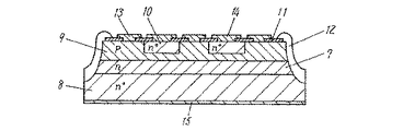
図2は本発明の実施の形態における封管拡散法を適用したメサ型半導体装置の断面図である。 FIG. 2 is a cross-sectional view of a mesa semiconductor device to which the sealed tube diffusion method in the embodiment of the present invention is applied.
上記ドライブイン処理後に得られたp型ベース領域9の表面濃度は5.0×1017cm-3であり、ボロンの拡散深さは28μm、アルミニウムの拡散深さは55μmであった。次いで、選択的にリンを拡散させて拡散深さ16μm、表面濃度4.0×1019cm-3のエミッタ拡散領域10を形成する。そして上記ベース領域9とエミッタ拡散領域10の上には二酸化珪素膜11を形成する。しかるのち、メサ溝形成領域の二酸化珪素膜を公知のフォトリソグラフィーとウエットエッチングあるいはドライエッチングにより除去し、室温以下に冷却された弗酸:硝酸:酢酸の混合液中で、水平揺動を行いながらエッチング処理して、メサ溝を形成する。
The surface concentration of the p-type base region 9 obtained after the drive-in process was 5.0 × 10 17 cm −3 , the boron diffusion depth was 28 μm, and the aluminum diffusion depth was 55 μm. Next, phosphorus is selectively diffused to form an
その後、スピンコーティング法により、アルミナ、二酸化珪素、酸化鉛からなるガラス粉末と感光性物質の混合液を厚み設定が100μmになるように塗布する。次に、露光・現像して塗布膜をパターニングし、電極形成部で塗布膜を除去し、メサ溝部のみに塗布膜を残るようにする。しかるのち、まず400℃、30分の酸化雰囲気で感光性物質を燃焼させて、メサ溝部にガラス粉末を残す。次いで、酸素、窒素雰囲気中で、900℃程度、15分間の熱処理を行い、ガラス粉末を焼成してガラス被膜12を形成する。最後に、ベース電極13、エミッタ電極14とコレクタ電極15をそれぞれ形成し、メサ型半導体装置を得る。
Thereafter, a glass powder composed of alumina, silicon dioxide, lead oxide and a photosensitive material is applied by spin coating so that the thickness is set to 100 μm. Next, the coating film is patterned by exposure and development, and the coating film is removed at the electrode forming portion so that the coating film remains only in the mesa groove portion. Thereafter, the photosensitive material is first burned in an oxidizing atmosphere at 400 ° C. for 30 minutes, leaving glass powder in the mesa groove. Next, heat treatment is performed at about 900 ° C. for 15 minutes in an oxygen and nitrogen atmosphere, and the glass powder is baked to form the
本実施の形態によれば、蒸気圧の高い弗化アルミニウムを包囲するようノンドープシリコン粉末を配置することで、ハロゲン化アルミニウムの過度の蒸発を抑制でき、石英封管内のAl蒸気の濃度差を少なくできるので、シリコン基板の面内および面間での不純物拡散のばらつきを大幅に低減することができる。 According to the present embodiment, by disposing non-doped silicon powder so as to surround aluminum fluoride having a high vapor pressure, excessive evaporation of aluminum halide can be suppressed, and the difference in concentration of Al vapor in the quartz sealed tube can be reduced. As a result, variations in impurity diffusion within and between the surfaces of the silicon substrate can be greatly reduced.
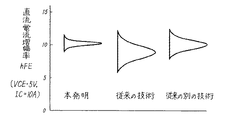
本実施の形態におけるNPNトランジスタ直流電流増幅率のばらつきを図3に示す。本実施形態の封管法はトランジスタのベース領域を形成する工程で使用した。 The variation of the NPN transistor direct current amplification factor in the present embodiment is shown in FIG. The sealed tube method of this embodiment was used in the process of forming the base region of the transistor.
なお、比較として、図3には、従来の技術、即ち不純物源としてボロン添加シリコン粉末と金属アルミニウムを用いてベース拡散層を形成したNPNトランジスタ、従来の別の技術、即ち不純物源としてボロン添加シリコン粉末とノンドープシリコンで包囲されていない弗化アルミニウムを用いてベース拡散層を形成したNPNトランジスタ直流電流増幅率のばらつきも示した。 For comparison, FIG. 3 shows a conventional technique, that is, an NPN transistor in which a base diffusion layer is formed using boron-doped silicon powder and metal aluminum as an impurity source, and another conventional technique, that is, boron-doped silicon as an impurity source. Also shown are variations in the DC current amplification factor of an NPN transistor in which a base diffusion layer is formed using aluminum fluoride not surrounded by powder and non-doped silicon.
図3に示すように、本実施の形態によれば、従来の拡散法で形成したトランジスタに比べて直流電流増幅率のばらつきを大幅に低減することがわかった。このことにより、製品の特性が安定化し、製造歩留を向上させることができる。 As shown in FIG. 3, according to the present embodiment, it has been found that the variation in the DC current gain is greatly reduced as compared with the transistor formed by the conventional diffusion method. As a result, the characteristics of the product can be stabilized and the manufacturing yield can be improved.
なお、本実施の形態ではメサ型NPNバイポーラトランジスタを例にとって説明したが、それ以外のデバイス、例えば通常のバイポーラトランジスタに適用しても本発明の効果は得られる。 In the present embodiment, a mesa type NPN bipolar transistor has been described as an example, but the effect of the present invention can be obtained even if it is applied to other devices such as a normal bipolar transistor.
また、シリコン基板の間に配置される不純物拡散源の位置は任意に設定されるものである。 Further, the position of the impurity diffusion source disposed between the silicon substrates is arbitrarily set.
本発明に係る半導体装置の製造方法は、不純物の拡散ばらつきを低減でき、バイポーラトランジスタ等の製造方法として有用である。 The method for manufacturing a semiconductor device according to the present invention can reduce the dispersion of impurity diffusion, and is useful as a method for manufacturing a bipolar transistor or the like.
1 シリコン基板
2 ボロン添加シリコン粉末
3 弗化アルミニウム
4 ノンドープシリコン粉末
5 石英管
6 金属アルミニウム
7 n型半導体領域(コレクタ領域)
8 n+型半導体領域(コレクタ領域)
9 p型半導体領域(ベース領域)
10 n+型半導体領域(エミッタ領域)
11 二酸化珪素
12 ガラス保護膜
13 ベース電極
14 エミッタ電極
15 コレクタ電極
1 Silicon substrate 2 Boron-doped silicon powder 3 Aluminum fluoride 4 Non-doped
8 n + type semiconductor region (collector region)
9 p-type semiconductor region (base region)
10 n + type semiconductor region (emitter region)
11
Claims (2)
Priority Applications (1)
| Application Number | Priority Date | Filing Date | Title |
|---|---|---|---|
| JP2004157414A JP4380418B2 (en) | 2004-05-27 | 2004-05-27 | Manufacturing method of semiconductor device |
Applications Claiming Priority (1)
| Application Number | Priority Date | Filing Date | Title |
|---|---|---|---|
| JP2004157414A JP4380418B2 (en) | 2004-05-27 | 2004-05-27 | Manufacturing method of semiconductor device |
Publications (2)
| Publication Number | Publication Date |
|---|---|
| JP2005340503A JP2005340503A (en) | 2005-12-08 |
| JP4380418B2 true JP4380418B2 (en) | 2009-12-09 |
Family
ID=35493719
Family Applications (1)
| Application Number | Title | Priority Date | Filing Date |
|---|---|---|---|
| JP2004157414A Active JP4380418B2 (en) | 2004-05-27 | 2004-05-27 | Manufacturing method of semiconductor device |
Country Status (1)
| Country | Link |
|---|---|
| JP (1) | JP4380418B2 (en) |
Families Citing this family (1)
| Publication number | Priority date | Publication date | Assignee | Title |
|---|---|---|---|---|
| CN109616512A (en) * | 2018-12-26 | 2019-04-12 | 瑞能半导体有限公司 | Semiconductor devices and its manufacturing method |
-
2004
- 2004-05-27 JP JP2004157414A patent/JP4380418B2/en active Active
Also Published As
| Publication number | Publication date |
|---|---|
| JP2005340503A (en) | 2005-12-08 |
Similar Documents
| Publication | Publication Date | Title |
|---|---|---|
| JP4380418B2 (en) | Manufacturing method of semiconductor device | |
| JPH06112146A (en) | Manufacture of diffusion type silicon element substrate | |
| JPH0368133A (en) | Solid phase diffusion | |
| JP3144891B2 (en) | Impurity diffusion method | |
| JP3584544B2 (en) | Method for manufacturing semiconductor device | |
| JPH03163821A (en) | Manufacture of semiconductor device | |
| JP2973958B2 (en) | Method for manufacturing semiconductor device | |
| JP2001110807A (en) | Method for forming thin insulation film | |
| JPS5850411B2 (en) | Impurity diffusion method | |
| JPS60175417A (en) | Manufacture of semiconductor device | |
| JP3272908B2 (en) | Method for manufacturing semiconductor multilayer material | |
| JPS609118A (en) | Manufacture of semiconductor device | |
| JPS58130567A (en) | Manufacture of semiconductor device | |
| JP2007242650A (en) | Vertical bipolar transistor and its fabrication process | |
| JPS59225566A (en) | Manufacture of semiconductor element | |
| JPS5927524A (en) | Fabrication of semiconductor device | |
| JPH07335584A (en) | Aluminum diffusion method to silicon substrate | |
| JP3191346B2 (en) | Manufacturing method of bonded substrate | |
| JPS5939901B2 (en) | Manufacturing method of semiconductor device | |
| JPS61294855A (en) | Manufacture of semiconductor device | |
| JPS5830735B2 (en) | Handout Taisouchino Seizouhouhou | |
| JPS5927106B2 (en) | Manufacturing method of semiconductor device | |
| JPH02252242A (en) | Manufacture of semiconductor device | |
| JPH04168764A (en) | Manufacture of semiconductor device | |
| JPS5969923A (en) | Diffusing method for boron |
Legal Events
| Date | Code | Title | Description |
|---|---|---|---|
| A621 | Written request for application examination |
Free format text: JAPANESE INTERMEDIATE CODE: A621 Effective date: 20070528 |
|
| RD01 | Notification of change of attorney |
Free format text: JAPANESE INTERMEDIATE CODE: A7421 Effective date: 20070613 |
|
| A131 | Notification of reasons for refusal |
Free format text: JAPANESE INTERMEDIATE CODE: A131 Effective date: 20090630 |
|
| A977 | Report on retrieval |
Free format text: JAPANESE INTERMEDIATE CODE: A971007 Effective date: 20090630 |
|
| A521 | Written amendment |
Free format text: JAPANESE INTERMEDIATE CODE: A523 Effective date: 20090806 |
|
| TRDD | Decision of grant or rejection written | ||
| A01 | Written decision to grant a patent or to grant a registration (utility model) |
Free format text: JAPANESE INTERMEDIATE CODE: A01 Effective date: 20090901 |
|
| A01 | Written decision to grant a patent or to grant a registration (utility model) |
Free format text: JAPANESE INTERMEDIATE CODE: A01 |
|
| A61 | First payment of annual fees (during grant procedure) |
Free format text: JAPANESE INTERMEDIATE CODE: A61 Effective date: 20090914 |
|
| FPAY | Renewal fee payment (event date is renewal date of database) |
Free format text: PAYMENT UNTIL: 20121002 Year of fee payment: 3 |
|
| FPAY | Renewal fee payment (event date is renewal date of database) |
Free format text: PAYMENT UNTIL: 20121002 Year of fee payment: 3 |