JP4354630B2 - CVD diamond-coated substrate for polishing pad conditioning head and method for producing the same - Google Patents
CVD diamond-coated substrate for polishing pad conditioning head and method for producing the same Download PDFInfo
- Publication number
- JP4354630B2 JP4354630B2 JP2000501874A JP2000501874A JP4354630B2 JP 4354630 B2 JP4354630 B2 JP 4354630B2 JP 2000501874 A JP2000501874 A JP 2000501874A JP 2000501874 A JP2000501874 A JP 2000501874A JP 4354630 B2 JP4354630 B2 JP 4354630B2
- Authority
- JP
- Japan
- Prior art keywords
- grit
- substrate
- diamond
- polishing pad
- conditioning head
- Prior art date
- Legal status (The legal status is an assumption and is not a legal conclusion. Google has not performed a legal analysis and makes no representation as to the accuracy of the status listed.)
- Expired - Fee Related
Links
Images


Classifications
-
- B—PERFORMING OPERATIONS; TRANSPORTING
- B24—GRINDING; POLISHING
- B24B—MACHINES, DEVICES, OR PROCESSES FOR GRINDING OR POLISHING; DRESSING OR CONDITIONING OF ABRADING SURFACES; FEEDING OF GRINDING, POLISHING, OR LAPPING AGENTS
- B24B53/00—Devices or means for dressing or conditioning abrasive surfaces
- B24B53/017—Devices or means for dressing, cleaning or otherwise conditioning lapping tools
-
- B—PERFORMING OPERATIONS; TRANSPORTING
- B24—GRINDING; POLISHING
- B24B—MACHINES, DEVICES, OR PROCESSES FOR GRINDING OR POLISHING; DRESSING OR CONDITIONING OF ABRADING SURFACES; FEEDING OF GRINDING, POLISHING, OR LAPPING AGENTS
- B24B37/00—Lapping machines or devices; Accessories
- B24B37/04—Lapping machines or devices; Accessories designed for working plane surfaces
-
- B—PERFORMING OPERATIONS; TRANSPORTING
- B24—GRINDING; POLISHING
- B24D—TOOLS FOR GRINDING, BUFFING OR SHARPENING
- B24D11/00—Constructional features of flexible abrasive materials; Special features in the manufacture of such materials
-
- B—PERFORMING OPERATIONS; TRANSPORTING
- B24—GRINDING; POLISHING
- B24D—TOOLS FOR GRINDING, BUFFING OR SHARPENING
- B24D18/00—Manufacture of grinding tools or other grinding devices, e.g. wheels, not otherwise provided for
- B24D18/0018—Manufacture of grinding tools or other grinding devices, e.g. wheels, not otherwise provided for by electrolytic deposition
Description
【0001】
本願は、1997年7月10日に出願された米国仮特許出願第60/052,145号の優先権主張出願である。
【0002】
〔発明の分野〕
本発明は、化学機械的平坦化(CMP)研磨パッド(ポリシングパッドと呼ばれることもある)のコンディショニングヘッド又はディスクの平らな基材に関する。本発明は、半導体ウェハやコンピュータハードディスクドライブに用いられるウェハ及びディスク上の誘電体及び半導体(酸化物)膜と金属膜の両方を平坦化すると共に(或いは)研磨するのに用いられる研磨パッドをコンディショニングすることができる。本発明は又、他の研磨サンダー仕上げ、研削仕上げ又は研磨ツールに用いられる十分なレベルの表面粗さを備えた連続CVDダイヤモンド被覆基材に関する。
【0003】
〔発明の背景〕
CMPは、半導体ウェハの製造費の大部分を占めている。これらCMPの費用としては、研磨パッド、研磨スラリー、パッド用コンディショニングディスク及び平坦化及び研磨作業中に摩耗する種々のCMP部品に関する費用がある。研磨パッド、パッドを交換するための操業停止時間、及びパッドを再校正するための試験用ウェハに関する全費用は、一回のウェハ研磨作業で約7ドルである。多くの複雑な集積回路デバイスでは、仕上げられたウェハ毎に最大5回のCMP作業が必要であり、これによりかかるウェハの総製造費が一段と増大する。
【0004】
研磨パッドに関する最も多くの摩耗量は、研磨パッドをこれらウェハの平坦化及び研磨作業に適した条件にするのに必要な研磨パッドのコンディショニングの結果として生じるものである。典型的な研磨パッドは、厚さが約1/16インチ(約1.59mm)の独立発泡又は気泡ポリウレタンフォームから成る。パッドのコンディショニング中、パッドに機械的な研磨処理を施してパッド表面の気泡層を物理的に切断する。パッドの露出表面は、使用済み研磨スラリーから成る研磨スラリー及びウェハから除去された物質を取り込む開放気泡又は微細孔を有している。次々に実施される各パッド研磨工程では、理想的なコンディショニングヘッドは、埋まっている物質を有する気泡の外側層だけを除去し、しかも、外側層の下に位置する層を全く除去することがないものである。かかる理想的なコンディショニングヘッドは、研磨パッドの層の除去を可能な限り最も少なくして、即ち、可能な限りパッドの摩耗率を少なくして100%の除去率を達成するであろう。パッドに関する摩耗の悪影響を考慮しなければ100%の除去率を達成できることは明らかである。しかしながら、かかるパッドの過剰の表面仕上げの結果として、パッドの寿命が短くなる。他方、表面仕上げが足りないと、CMP工程中の材料除去率が不十分となり、摩耗の均一性が失われる。満足の行く除去率を達成する従来型コンディショニングヘッドを用いると、パッドが役に立たなくなって交換しなければならなくなる前に、特定の操業条件に応じるものの、200〜300回という少ない回数及び数千回という多い回数のウェハ研磨作業を行うことができる。交換時期は、パッドをその元々の厚さのほぼ1/2に減らした後に生じる。
【0005】
高いウェハ除去率と低いパッド摩耗率の理想的なバランスに近いレベルを達成し、コンディショニングの品質を損なわないで研磨パッドの有効寿命を大幅に伸ばすことができるようにするコンディショニングヘッドが非常に要望されている。
【0006】
従来型コンディショニングヘッドは典型的には、ステンレス鋼板と、このステンレス鋼板の表面上にむらがある状態で分布されたダイヤモンドグリットと、ステンレス鋼板及びダイヤモンドグリットを被覆する湿式化学法によりめっきされたニッケルの保護被膜とから成る。かかる従来型コンディショニングヘッドの使用は、酸化物CMPウェハ加工中、即ち、露出した外側層が金属ではなく酸化物含有材料である場合に用いられた研磨パッドのコンディショニングに制限される。半導体ウェハの加工の際、ほぼ同一回数の酸化物と金属CMP加工工程が実施される。しかしながら、従来型コンディショニングヘッドは、金属加工作業に関するコンディショニングには使えない。この理由は、ウェハからの材料の除去に用いられるスラリーがニッケルと反応を起こし、コンディショニングヘッドのニッケル外側層を劣化させたり溶解させ、それによりステンレス鋼板からダイヤモンドグリットを大部分失わせ、ウェハに掻き傷をつける恐れがあるからである。
【0007】
酸化物含有ウェハ表面と金属含有ウェハ表面の両方をコンディショニングするのに有効なヘッドに対する要望が高い。また、ダイヤモンドグリットをその下に位置する基材に一層しっかりと取り付けられているコンディショニングヘッドが非常に要望されている。また、CMP作業中に所与のウェハからのウェハ材料の除去における均等性の度合いを大きくするコンディショニングヘッドが要望されている。最後に、研磨パッドの寿命を伸ばすコンディショニングヘッドが要望されている。
【0008】
〔発明の概要〕
本発明は、ウェハ除去率を損なわないで研磨パッドの寿命を二倍にすることが判明したCMP装置及びこれに類似した形式の装置用研磨パッドコンディショニングヘッド及び研磨パッドコンディショニングヘッドの作製方法に関する。加うるに、本発明のコンディショニングヘッドは、(1)酸化物表面だけでなく金属表面を加工するのに用いられる研磨パッドのコンディショニングに有効であり、(2)ダイヤモンドグリットが基材に一層しっかりと取り付けられ、その結果、基材から取れてウェハに潜在的に掻き傷をつけることがないように作製され、(3)所与のウェハ全体からの材料の除去における均等性の度合いを大きくする。
【0009】
CMP装置及びこれと類似した装置において、基材と、基材上に実質的に一様に分布したダイヤモンドグリットの単一層と、その結果得られたグリット被覆基材上に、前記ダイヤモンドグリットを包み込むと共に該ダイヤモンドグリットを前記基材に接合するよう化学気相成長させたダイヤモンドの外側層とから成る研磨パッドコンディショニングヘッドが提供される。
【0010】
「化学気相成長(CVD)」という用語は、真空蒸着法により蒸着される材料を意味し、かかる真空蒸着法としては、反応性ガス状前駆物質からの熱活性蒸着法、プラズマ法、マイクロ波法、及びガス状前駆物質からのDC又はRFプラズマアークジェット蒸着法が挙げられる。
【0011】
〔発明の好ましい実施形態の説明〕
図1に示すCMP装置10は、研磨パッド14がしっかりと取り付けられた定盤12を有している。研磨パッド14は、例えば時計回りの方向に回転する状態で示されている。ウェハ18を備えた半導体ウェハホルダー16が、ウェハ18をパッド14の露出表面に押し付けてこれを保持するよう示された状態で位置している。ホルダー16は、例えば反時計回りの方向に回転する状態で示されている。ウェハ18は、真空又は当該技術分野で周知の他の手段によりホルダー16に固定されている。研磨スラリー20が、導管22のノズルを通してパッド14の中央領域内に計量分配される。スラリー20は代表的には、適当な液体、例えば水で稀釈した水酸化カリウム中に分散した二酸化珪素から成る。スラリーの正確な組成は、ウェハの露出表面の所望の平坦化を可能にするよう厳密に計算されている。装置10はウェハホルダーを1つだけ示しているが、CMP装置は、複数のホルダーを有するものとして市販されている。
【0012】
研磨パッドのコンディショニングヘッド又はディスク24が、基材26の表面上に一様に分布された天然又は合成ダイヤモンドグリット28と、グリット28及び基材26上に成長させたCVD多結晶質ダイヤモンド(以下、「CVDダイヤモンド」という)の連続薄膜30とを有し、したがってグリット28は、CVDダイヤモンド30で包み込まれた状態で基材26の表面に接合されている。
【0013】
CVDダイヤモンドの一様な層30が、1993年2月16日に発行されたガーグ氏等の米国特許第5,186,973号に記載された形式の熱フィラメントCVD(HFCVD)反応器を用いて基材26の露出表面上に成長させる。かかる米国特許明細書のうち基材上へのCVDダイヤモンドの成長に関する記載部分を本明細書の一部を形成するものとして引用する。
【0014】
好ましくは、CVDダイヤモンドを、基材の表面上に化学的に気相成長(化学的に蒸着)させ、CVDダイヤモンド層が、工業等級のダイヤモンドの表面上に(220)又は(311)方向及び(400)方向の明確な結晶方位を呈するようになっている。「化学的に気相成長させる」又は「化学的に蒸着させる」という用語は、水素と炭素化合物、好ましくは炭化水素の供給ガス混合物が、実質的に黒鉛状炭素蒸着を避けるような仕方で活性化された気相からのダイヤモンド生成炭素原子に分解することによって起こるCVDダイヤモンドの層の蒸着を意味する。炭化水素の好ましい種類としては、C1 〜C4 飽和炭化水素、例えばメタン、エタン、プロパン及びブタン、C1 〜C4 不飽和炭化水素、例えばアセチレン、エチレン、プロピレン及びブチレン、C及びOを含むガス、例えば一酸化炭素及び二酸化炭素、芳香族化合物、例えばベンゼン、トルエン、キシレン等、及びC、H及び少なくとも1つの炭素及び/又は窒素を含む有機化合物、例えばメタノール、エタノール、プロパノール、ジメチルエーテル、ジエチルエーテル、メチルアミン、エチルアミン、アセトン及び類似の化合物が挙げられる。水素ガス中の炭素化合物の濃度は、約0.01%〜約10%、好ましくは約0.2%〜約5%、より好ましくは約0.5%〜約2%であるのがよい。HFCVD蒸着法で結果的に得られるダイヤモンド膜は、接着性の個々の結晶又は実質的に粒間接着結合剤の無い層状の微結晶凝集体の形態をしている。
【0015】
CVDダイヤモンドの全厚は、グリットサイズの少なくとも約10%である。好ましくは、ダイヤモンド膜の全厚は、約10〜250ミクロンである。さらにより好ましくは、これは約20〜30ミクロンである。
【0016】
HFCVD法は、炭化水素と水素の混合物を含む供給ガス状混合物を加熱された状態のフィラメントで活性化し、活性化されたガス状混合物を加熱された基材上に流して多結晶質ダイヤモンド膜を蒸着させる。水素中に0.1%〜約10%の炭化水素を含む供給ガス状混合物を減圧下で、即ち100トル以下において熱の作用で活性化させて炭化水素ラジカル及び水素原子をW、Ta、Mo、Re又はこれらの混合物で作られた加熱状態のフィラメントを用いて生じさせる。フィラメントは、約1800℃〜2800℃の範囲にある。基材を約600℃〜約1100℃の蒸着温度まで加熱する。
【0017】
珪素基材上にCVDダイヤモンドを単純に成長させることに起因する表面粗さは、厚さ20ミクロンのCVDダイヤモンドを有する基材上に最上部から最下部まで約6〜約12ミクロンの範囲にある。一般に、典型的な作業のための表面粗さは、基材上に成長させたCVDダイヤモンドの厚さの約1/4〜約1/2の範囲にある。この度合の表面粗さは低すぎるので、CMPコンディショニング作業に合った所望の研磨効率を得ることができない。本発明では、天然ダイヤモンドのカッティング及び高圧法を用いる工業等級のダイヤモンドから得ることができるダイヤモンドグリットをCVD薄膜の組織中へ導入する。グリットのサイズは、最上部と最下部の表面間距離がCVDダイヤモンド膜の厚さよりも大きくなるように選択されている。ダイヤモンドグリットを、個々の結晶粒を平均結晶粒直径の1/2以上もの距離だけ離すような密度で基材の表面上に一様に分布させる。ダイヤモンドグリットの平均サイズは、約15ミクロン〜約150ミクロンの範囲にあり、好ましくは約35ミクロン〜約70ミクロンの範囲にある。ダイヤモンドグリットのサイズ及び密度を制御することにより、その結果得られる表面の研磨特性を種々のコンディショニング用途に合わせて調節することができる。所与のディスク上の結晶粒度は、約±20%に等しいであろう。
【0018】
図2は、ダイヤモンドグリット28の非均一層を支持板32、例えばステンレス鋼板の表面上に分布させ、ニッケルめっき33を湿式化学プロセスによって蒸着させてダイヤモンドグリット28を支持板32に不安定な状態で接合する。
【0019】
図3は、支持板32の使用が任意であることを除き、上述のコンディショニングヘッド24と実質的に同一の組成のものであるコンディショニングディスク34の横断面を示している。基材26は、CVDダイヤモンドを成長させるものとして知られた任意の材料から成り、かかる基材26としては、例えば炭化珪素、焼結カーバイド、炭化タングステン、珪素、サファイヤ及び類似の物質が挙げられる。基材は通常は、直径が約2インチ〜4インチ(約5.08cm〜約10.16cm)の範囲にあるディスクの形態をしている。しかしながら、コンディショニングヘッドのための基材として他の形状を用いた。基材26の厚さは、約0.02インチ〜約0.25インチ(約0.508mm〜6.35mm)の範囲にあり、好ましくは約0.04インチ〜約0.25インチ(約1.016mm〜6.35mm)の範囲にあり、好ましくは0.04インチ〜0.08インチ(約1.016mm〜2.032mm)の範囲にある。1mm2当たりの結晶粒の数が約0.1〜約50個、好ましくは約1〜30個の密度でダイヤモンドグリット28の単一層を基材26の表面上に一様に分布させ、外側ダイヤモンド層30をグリット28及び基材26上に化学気相成長させた後、コンディショニングディスク34の全厚を約40〜約150ミクロンに増大させる。珪素から成る基材の場合、珪素をコンディショニングディスク34に一層の安定性を与える周知の接着剤を用いて支持板32に接合する場合が多い。代表的には、支持板32は、厚さが約0.04〜0.08インチの磁性ステンレス鋼から成る。
【0020】
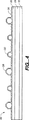
図4は、本発明の別の実施形態のコンディショニングディスク40の横断面を示しており、かかる実施形態では、先ず最初にCVDダイヤモンドの中間層35を基材26上に被着し、次にダイヤモンドグリット28をCVDダイヤモンド中間層35の露出表面全体上に一様に分布させる。コンディショニングディスク34の作製の際に上述した残りの工程を繰り返して、その結果ディスク40内でダイヤモンドグリットの粒子28が、CVDダイヤモンドの外側層30がグリット28上に成長する前に、CVDダイヤモンド中間層35へのダイヤモンド粒子の接着性の向上により互いに近接して配置できる。この実施形態は、サイズが100ミクロン以上のダイヤモンドグリットを用いる場合に有効である。
【0021】
図5A及び図5Bは、本発明の更に別の実施形態のコンディショニングディスク50の横断面を示しており、かかる実施形態では、先ず最初に結晶粒度が約40ミクロン〜約150ミクロンの大きなダイヤモンドグリット28の単一層を基材26の露出表面全体上に一様に分布させ、次に粒度が1ミクロン未満の小さなグリット36を1mm2当たりの結晶粒の数が約5000個以上の密度でダイヤモンドグリット28及び基材26の露出表面全体上に一様に分布させる。次に、CVDダイヤモンドを図5Aに示すようにダイヤモンドグリット36及びダイヤモンドグリット28上に成長させ、外側層30がエピタキシャル成長したダイヤモンドに代わって多結晶質ダイヤモンドになっている。本発明のディスク50は、ダイヤモンドグリット28とCVDダイヤモンド結合層又は外側層30との間の接合性が向上している。
【0022】
図6は、本発明の別の実施形態を示しており、かかる実施形態では、ディスク60は第1の側部62及び第2の側部64を備えた基材26を有し、これら両方の側部はダイヤモンドグリット28で被覆されると共にCVDダイヤモンド30で包み込まれている。この実施形態では、両側部62,64上にダイヤモンドグリット28を有する基材26を、当該技術分野で周知の仕方で両方の側部が供給ガス状混合物にさらされるようにCVD反応器内へ取り付けるのがよい。変形例として、基材26をダイヤモンドグリットで被覆した第1の側部62を露出させた状態でCVD反応器内に配置し、第1の側部を第1の工程でCVDダイヤモンド30で包み込む。次いで、ダイヤモンドグリットで被覆された第2の側部64を露出させた状態で第1の工程を繰り返し、第2の側部を第2の工程で包み込む。ディスク50を、両側ポリッシャの状態で用いられるコンディショニング研磨パッド、例えばシリコンウェハ及びコンピュータのハードディスクドライブで用いられるディスクを研磨するためのパッド用として用いることができる。
【0023】
図7、図7A及び図8は、等間隔を置いた形状、例えばドット52のパターンを有するシールド50を用いてウェハ26の露出表面全体上へのダイヤモンドグリット28の集中領域の非常に一様な分布を得るために用いられる本発明の実施形態を示している。ドット52はまた、正方形、渦巻き型、棒状及び他の形状をしていてもよい。シールド50は任意の材料、好ましくは熱可塑性樹脂でできたものであるのがよい。
【0024】
〔対照例及び実施例〕
対照例及び実施例並びに以下の説明は、従来技術のコンディショニングヘッドと比較した場合の本発明のコンディショニングヘッドの優れた性能を更に示している。対照例及び実施例は、例示の目的のためであって、請求の範囲に記載された本発明の範囲をいかなる意味においても限定するものではない。
【0025】
〔対照例1〕
図2に示し、サンプル−マーシャル(Sample−Marshall)100グリットディスクとして市販されている形式の従来型コンディショニングディスクをモデル6DS−SPストラスバーグ・プラナイザ(Strasbaugh Plaizer)のコンディショニングアームに取付けて、標準の除去率及び研磨パッド摩耗率を測定するための試験を行った。ディスクの直径は4インチ(10.16cm)であり、これには湿式化学プロセスを用いて磁性ステンレス鋼板に平均サイズが100ミクロンのニッケルめっきされた約120,000個のダイヤモンド粒子を有していた。この標準型コンディショニングディスクに関する結果の示すところによれば、研磨パッドの摩耗率は、最高2000個のウェハを1分間当たり約1800オングストロームのウェハ材料除去率で研磨できた。
【0026】
〔対照例2〕
直径が4インチ(10.16cm)、厚さが0.25インチ(6.35mm)の炭化タングステンディスクを機械加工して、隆起した正方形のグリッドを形成し、正方形相互間にはトレンチが存在した。機械加工したディスクを、全体構成が上述のガーグ氏等の米国特許第5,186,973号に記載されている形式のものであって、これを1995年12月20日に出願され、本出願人であるエスピー3・インコーポレイテッドに譲渡されているハーリンガー氏等の米国特許出願第08/575,763号の教示に従って設計変更したHFCVD反応器の支持取付け具上に平らに置いた。反応器を閉じ、15.95kw(145ボルト及び110アンペア)を供給してフィラメントを約2000℃に加熱した。72sccm(立方センチメートル毎分(標準状態下))のメタンと3.0slpm(リットル毎分(標準状態下))で約2.5体積%の水素の混合物を30トルの圧力で1時間半をかけて反応器内に供給し、約1〜2ミクロンの多結晶質ダイヤモンドを、隆起した正方形を含む機械加工ディスクの露出表面上に蒸着させた。電力を、更に21時間半をかけて25トルの圧力状態で21.24kw(177ボルト及び120アンペア)に増大させた。フィラメントへの電力供給を停止し、被覆状態のウェハを流動中の水素ガス下で室温まで冷却した。全部で10〜15ミクロンのコヒーレントな多結晶質ダイヤモンドをウェハ上に蒸着させた。その結果得られたコンディショニングディスクは、各側部上に約0.125インチ(約3.18mm)の隆起した正方形を有し、隆起した正方形の間には0.125インチのトレンチが存在した。ディスクを、モデル6DS−SPストラスバーグ・プラナイザ(Strasbaugh Planizer)のコンディショニングアームに取り付け、対照例1において記載したステンレス鋼板上に被着されたニッケルメッキダイヤモンドグリットを有する標準型コンディショニングディスクと比較してその有効性を判定するために試験した。このディスクを用いた結果の示すところによれば、材料除去率は標準コンディショニングディスクを用いた場合の代表的な除去率の約63%であった。研磨パッドに関する摩耗については目立った差はなかった。
【0027】
〔対照例3〕
フォトレジストの層を、多結晶質珪素基材上に被着させ、露光して現像し、角錐状のパターンを形成し、次に、硬いダイヤモンド膜をアッペル氏等の米国特許第5,536,202号に教示されている方法を用いてパターン化された基材上に成長させるとコンディショニングディスクを形成することができる。類似のパターン化されたディスクを用いる予備実験から得られた結果に基づいて判断するところによれば、かかるコンディショニングディスクは、標準のコンディショニングディスクの除去率を達成することはできないものと思われる。
【0028】
〔実施例1〕
直径が4インチ、厚さが0.04インチ(約1mm)の珪素基材を、上述のガーグ氏等の米国特許第5,186,973号に記載されている形式のものであって、これを上述のハーリンガー氏等の米国特許出願第08/575,763号の教示に従って設計変更したHFCVD反応器の支持取付け具上に平らに配置した。平均粒径が約50ミクロンの合成ダイヤモンドグリットの単一層を、珪素基材の第1の側部の露出表面全体上に一様に分布し、1mm2当たりの結晶粒又はグリット粒子の数が20個及び15〜30個の範囲にわたる平均グリット密度を達成した。容器からのグリットを、空気分散法を用いて一様に分布させた。かかる空気分配法では、グリットを一定の高さ、即ちウェハよりも3インチ(7.62cm)上の高さから制御された速度で落下させた。移動中の空気流を用いてグリットを基材全体上に横方向に分散させた。グリットをウェハ上に落下させながらグリット容器を空気流の方向と直交する方向に移動させて、基材の露出表面全体にグリットの一様な分布を得た。基材を、この空気分散法を繰り返しながら90°の回転を3回行った。グリットの密度を、グリット供給速度と基材の並進速度の両方によって制御する。変形例として、基材を、グリットをウェハ上に落下させながら、直交方向に移動させて基材の露出表面全体上にグリットの一様な分布を得てもよい。
【0029】
次に基材をCVDダイヤモンド蒸着反応器内に配置する。反応器を閉じ、15.95kw(145ボルト及び110アンペア)を供給してフィラメントを約2000℃に加熱した。72sccm(立方センチメートル毎分(標準状態下))のメタンと3.0slpm(リットル毎分(標準状態下))の水素の混合物を30トルの圧力で1時間半をかけて反応器内に供給し、約1〜2ミクロンの多結晶質ダイヤモンドを、隆起した正方形を含む機械加工ディスクの露出表面上に蒸着させた。電力を、更に21時間半をかけて25トルの圧力状態で21.24kw(177ボルト及び120アンペア)に増大させた。フィラメントへの電力供給を停止し、被覆状態のウェハを流動中の水素ガス下で室温まで冷却した。全部で10〜15ミクロンのコヒーレントな多結晶質ダイヤモンドをウェハ上に蒸着させた。この工程から得られたディスクの第2の側部を図3に示すように支持層に接合した。その結果得られたコンディショニングヘッド34を、モデル6DS−SPストラスバーグ・プラナイザのコンディショニングアームに取り付け、ステンレス鋼板上に被着されたニッケルメッキダイヤモンドグリットを有する標準型コンディショニングディスクと比較してその有効性を判定するために試験した。予想外のこととして、かかる結果の示すところによれば、研磨パッドの摩耗率は標準コンディショニングディスクを用いた場合の摩耗率の42%であった。この実施例1のディスクは、標準型コンディショニングディスクの場合と実質的に等しいウェハ材料除去率を達成した。
【0030】
〔実施例2〕
多結晶質ダイヤモンドを珪素基材上に成長させて被覆状態のウェハを室温まで冷却させた後、合成ダイヤモンドグリットを珪素基材の第1の側部上に一様に分布させたことを除き、実施例1の手順を繰り返した。平均粒径が約100ミクロンの合成ダイヤモンドグリットの単一層を、上述の実施例1の空気分散法を用いて、珪素基材の露出表面全体上に一様に分布し、1mm2当たりの結晶粒又はグリット粒子の数が2.5個及び0〜6個の範囲にわたる平均グリット密度を達成した。反応器を閉じ、15.95kw(145ボルト及び110アンペア)を供給してフィラメントを約2000℃に加熱した。65sccm(立方センチメートル毎分(標準状態下))のメタンと3.0slpm(リットル毎分(標準状態下))の水素の混合物を30トルの圧力で1時間半をかけて反応器内に供給し、約1〜2ミクロンの多結晶質ダイヤモンドを、ダイヤモンドグリット及び珪素基材の露出表面上に蒸着させた。電力を、更に21時間半をかけて25トルの圧力状態で21.24kw(177ボルト及び120アンペア)に増大させた。フィラメントへの電力供給を停止し、被覆状態のウェハを流動中の水素ガス下で室温まで冷却した。全部で10〜15ミクロンのコヒーレントな多結晶質ダイヤモンドをウェハ上に蒸着させた。この工程から得られたディスクの第2の側部を図4に示すように支持層に接合した。その結果得られたコンディショニングヘッド40を、モデル6DS−SPストラスバーグ・プラナイザのコンディショニングアームに取り付け、ステンレス鋼板上に被着されたニッケルメッキダイヤモンドグリットを有する標準型コンディショニングディスクと比較してその有効性を判定するために試験した。パッドの摩耗率は標準コンディショニングディスクを用いた場合のパッド摩耗率の半分であった。この実施例2のコンディショニングヘッドは、標準型コンディショニングディスクの場合と実質的に等しいウェハ材料除去率を維持した。また、ウェハ研磨の均一性は、標準方法よりも優れていたことが分かった。
【0031】
〔実施例3〕
実施例1の手順を基材の第1の側部の露出表面に対して繰り返したが、異なる点として、その結果得られたディスクの第2の側部を図3に示すような支持層に接合しなかった。その代わりに、実施例1の手順をディスクの第2の側部の露出表面に対して繰り返し行って図6に示すような両側コンディショニングディスクを作製した。この基材は、シリコンウェハ又はハードディスクドライブのメディア用ディスクと同一の直径及び厚さに合わせて形作られる。。この場合、基材の直径は100mm、厚さは0.025インチであった。次に、仕上げられたコンディショニングヘッドを、普通の製品と同様にして両側ポリッシャ内へ装入し、研磨パッドの両方を同時にコンディショニングした。
【0032】
〔実施例4〕
実施例1の手順を基材の第1の側部の露出表面に対して繰り返したが、異なる点として、この表面の選択された領域を、等間隔に配置されたパターン正方形を有するプラスチックシールド(図7及び図7Aに示すドットに代えて用いた)によって保護した。シールドは、グリットがウェハの表面上の或る特定の領域に達することがないようにする。また、これにより、グリットの非常に一様なパターンの集中した正方形がウェハの表面上に生じることが可能となる。この実施例の手順は、研磨パッドとその結果得られた本発明のこの実施形態のコンディショニングディスクとの間のスラリー移動具合を向上させるのに有効であることが分かった。
【0033】
本発明の精神及び範囲から逸脱しないで、当業者であれば、本発明を種々の用途及び条件に合わせるよう本発明の種々の設計変更及び改造を行うことができる。したがって、これら設計変更例及び改造例は、請求の範囲に記載された本発明の均等範囲に適法に含まれるものである。
【図面の簡単な説明】
【図1】 本発明のCMP装置を示す図である。
【図2】 従来技術の研磨パッドコンディショニングヘッドの断面図である。
【図3】 本発明の一実施形態の研磨パッドコンディショニングヘッドの断面図である。
【図4】 本発明の別の実施形態の研磨パッドコンディショニングヘッドの断面図である。
【図5A】 本発明の更に別の実施形態の研磨パッドコンディショニングヘッドの断面図である。
【図5B】 図5Aに示す研磨パッドコンディショニングヘッドの詳細断面図である。
【図6】 本発明の別の実施形態の研磨パッドコンディショニングヘッドの断面図である。
【図7】 本発明の別の実施形態で用いられるパターン付けされたシールドの平面図である。
【図7A】 ウェハ上の図7のパターン付けされたシールドを示す図である。
【図8】 図7Aのパターン付けされたシールドの断面図であり、ウェハ上のダイヤモンドグリットの分布状態を示す図である。[0001]
This application is a priority application of US Provisional Patent Application No. 60 / 052,145 filed on July 10, 1997.
[0002]
(Field of the Invention)
The present invention relates to a chemical mechanical planarization (CMP) polishing pad (sometimes referred to as a polishing pad) conditioning head or disk flat substrate. The present invention conditions a polishing pad used to planarize and / or polish both dielectric and semiconductor (oxide) films and metal films on wafers and disks used in semiconductor wafers and computer hard disk drives. can do. The present invention also relates to a continuous CVD diamond coated substrate with a sufficient level of surface roughness used in other polishing sander finishes, grinding finishes or polishing tools.
[0003]
BACKGROUND OF THE INVENTION
CMP accounts for most of the manufacturing cost of semiconductor wafers. These CMP costs include costs for polishing pads, polishing slurries, pad conditioning disks and various CMP components that wear during planarization and polishing operations. The total cost for the polishing pad, the downtime to replace the pad, and the test wafer to recalibrate the pad is about $ 7 in a single wafer polishing operation. Many complex integrated circuit devices require up to five CMP operations per finished wafer, which further increases the total manufacturing cost of such wafers.
[0004]
The greatest amount of wear associated with the polishing pad is the result of the conditioning of the polishing pad necessary to bring the polishing pad to conditions suitable for these wafer planarization and polishing operations. A typical polishing pad consists of a closed foam or cellular polyurethane foam having a thickness of about 1/16 inch (about 1.59 mm). During pad conditioning, the pad is mechanically polished to physically cut the bubble layer on the pad surface. The exposed surface of the pad has a polishing slurry of spent polishing slurry and open bubbles or micropores that take up material removed from the wafer. In each successive pad polishing step, the ideal conditioning head removes only the outer layer of bubbles with embedded material, and does not remove any layers underlying the outer layer. Is. Such an ideal conditioning head would achieve 100% removal with the least possible removal of the polishing pad layer, ie, with as little pad wear as possible. It is clear that 100% removal rate can be achieved without considering the adverse effects of wear on the pad. However, as a result of the excessive surface finish of such pads, the life of the pads is shortened. On the other hand, if the surface finish is insufficient, the material removal rate during the CMP process becomes insufficient and the wear uniformity is lost. With a conventional conditioning head that achieves a satisfactory removal rate, depending on the specific operating conditions before the pad becomes useless and has to be replaced, as few as 200-300 times and thousands of times A large number of wafer polishing operations can be performed. The replacement time occurs after the pad has been reduced to approximately one half of its original thickness.
[0005]
There is a great need for a conditioning head that achieves a level close to the ideal balance of high wafer removal rate and low pad wear rate, and that can significantly extend the useful life of the polishing pad without compromising the quality of the conditioning. ing.
[0006]
Conventional conditioning heads typically include a stainless steel plate, diamond grit distributed with unevenness on the surface of the stainless steel plate, and nickel plated by a wet chemical method that coats the stainless steel plate and diamond grit. It consists of a protective coating. The use of such conventional conditioning heads is limited to conditioning of polishing pads used during oxide CMP wafer processing, i.e., when the exposed outer layer is an oxide-containing material rather than a metal. When processing a semiconductor wafer, approximately the same number of oxide and metal CMP processing steps are performed. However, conventional conditioning heads cannot be used for conditioning related to metalworking operations. This is because the slurry used to remove material from the wafer reacts with the nickel, which degrades and dissolves the nickel outer layer of the conditioning head, thereby largely losing diamond grit from the stainless steel plate and scraping the wafer. This is because there is a risk of scratching.
[0007]
There is a great need for a head that is effective in conditioning both oxide-containing and metal-containing wafer surfaces. There is also a great need for a conditioning head in which the diamond grit is more firmly attached to the underlying substrate. There is also a need for a conditioning head that increases the degree of uniformity in the removal of wafer material from a given wafer during a CMP operation. Finally, there is a need for a conditioning head that extends the life of the polishing pad.
[0008]
[Summary of the Invention]
The present invention relates to a CMP apparatus that has been found to double the life of a polishing pad without impairing the wafer removal rate, a polishing pad conditioning head for an apparatus of a type similar to the CMP apparatus, and a method of manufacturing the polishing pad conditioning head. In addition, the conditioning head of the present invention is (1) effective in conditioning polishing pads used to process metal surfaces as well as oxide surfaces, and (2) diamond grit is more firmly attached to the substrate. Are attached and, as a result, are made so that they can be removed from the substrate and not potentially scratch the wafer, and (3) increase the degree of uniformity in the removal of material from the entire given wafer.
[0009]
In a CMP apparatus and similar apparatus, the diamond grit is encased on a substrate, a single layer of diamond grit distributed substantially uniformly on the substrate, and the resulting grit coated substrate. And a polishing pad conditioning head comprising an outer layer of diamond that has been chemically vapor deposited to bond the diamond grit to the substrate.
[0010]
The term “chemical vapor deposition (CVD)” means a material that is deposited by vacuum deposition, which includes thermally activated deposition from reactive gaseous precursors, plasma, microwaves. And DC or RF plasma arc jet deposition from gaseous precursors.
[0011]
DESCRIPTION OF PREFERRED EMBODIMENTS OF THE INVENTION
A
[0012]
A polishing pad conditioning head or disk 24 includes natural or
[0013]
A
[0014]
Preferably, CVD diamond is chemically vapor deposited (chemically deposited) on the surface of the substrate so that the CVD diamond layer is oriented on the surface of industrial grade diamond in the (220) or (311) direction and ( The crystal orientation of the (400) direction is clear. The terms “chemically vapor-grown” or “chemically vapor-deposited” are used in such a way that the feed gas mixture of hydrogen and carbon compound, preferably hydrocarbon, substantially avoids graphitic carbon deposition. It means the deposition of a layer of CVD diamond which takes place by decomposition into diamond-generated carbon atoms from the vaporized gas phase. Preferred types of hydrocarbons include C 1 ~ C Four Saturated hydrocarbons such as methane, ethane, propane and butane, C 1 ~ C Four Unsaturated hydrocarbons such as acetylene, ethylene, propylene and butylene, gases containing C and O, such as carbon monoxide and carbon dioxide, aromatics such as benzene, toluene, xylene and the like, C, H and at least one carbon And / or organic compounds containing nitrogen, such as methanol, ethanol, propanol, dimethyl ether, diethyl ether, methylamine, ethylamine, acetone and similar compounds. The concentration of the carbon compound in the hydrogen gas should be about 0.01% to about 10%, preferably about 0.2% to about 5%, more preferably about 0.5% to about 2%. The resulting diamond film obtained by HFCVD deposition is in the form of layered microcrystalline aggregates that are adherent individual crystals or substantially free of intergranular adhesive binders.
[0015]
The total thickness of the CVD diamond is at least about 10% of the grit size. Preferably, the total thickness of the diamond film is about 10 to 250 microns. Even more preferably, this is about 20-30 microns.
[0016]
The HFCVD method activates a feed gaseous mixture containing a mixture of hydrocarbons and hydrogen with heated filaments and flows the activated gaseous mixture over a heated substrate to produce a polycrystalline diamond film. Evaporate. A feed gas mixture containing 0.1% to about 10% hydrocarbon in hydrogen is activated under reduced pressure, ie, under 100 Torr, by the action of heat to convert hydrocarbon radicals and hydrogen atoms to W, Ta, Mo. , Re, or a mixture of these to produce a heated filament. The filament is in the range of about 1800 ° C to 2800 ° C. The substrate is heated to a deposition temperature of about 600 ° C to about 1100 ° C.
[0017]
Surface roughness resulting from simply growing CVD diamond on a silicon substrate ranges from about 6 to about 12 microns from the top to the bottom on a substrate having a CVD diamond thickness of 20 microns. . In general, the surface roughness for typical operations is in the range of about 1/4 to about 1/2 the thickness of CVD diamond grown on the substrate. This degree of surface roughness is too low to provide the desired polishing efficiency for the CMP conditioning operation. In the present invention, diamond grit obtainable from industrial grade diamond using natural diamond cutting and high pressure methods is introduced into the structure of the CVD thin film. The size of the grit is selected such that the distance between the top and bottom surfaces is greater than the thickness of the CVD diamond film. The diamond grit is uniformly distributed on the surface of the substrate at a density such that the individual grains are separated by a distance of at least half the average grain diameter. The average size of the diamond grit is in the range of about 15 microns to about 150 microns, and preferably in the range of about 35 microns to about 70 microns. By controlling the size and density of the diamond grit, the resulting surface polishing properties can be tailored for various conditioning applications. The grain size on a given disk will be equal to about ± 20%.
[0018]
FIG. 2 shows that a non-uniform layer of
[0019]
FIG. 3 shows a cross-section of a conditioning disk 34 that is of substantially the same composition as the conditioning head 24 described above, except that the use of the
[0020]
FIG. 4 shows a cross section of a
[0021]
FIGS. 5A and 5B show a cross-section of a
[0022]
FIG. 6 illustrates another embodiment of the present invention, in which the
[0023]
FIGS. 7, 7A and 8 show a very uniform area of concentration of
[0024]
[Control Examples and Examples]
The control and examples and the following description further illustrate the superior performance of the conditioning head of the present invention as compared to prior art conditioning heads. The controls and examples are for illustrative purposes and do not limit the scope of the invention as claimed in any way.
[0025]
[Control Example 1]
A conventional conditioning disc of the type shown in FIG. 2 and marketed as a Sample-Marshall 100 grit disc is attached to the conditioning arm of a Model 6DS-SP Strasberg Planizer to remove the standard. Tests were performed to measure the rate and polishing pad wear rate. The diameter of the disk was 4 inches (10.16 cm), which had about 120,000 diamond particles nickel-plated on a magnetic stainless steel plate with an average size of 100 microns using a wet chemical process. . The results for this standard conditioning disk show that the polishing pad wear rate was able to polish up to 2000 wafers with a wafer material removal rate of about 1800 angstroms per minute.
[0026]
[Control Example 2]
Tungsten carbide discs 4 inches (10.16 cm) in diameter and 0.25 inches (6.35 mm) thick were machined to form raised square grids with trenches between the squares . The machined disc is of the type described in U.S. Pat. No. 5,186,973 to Garg et al., Described above, which was filed on Dec. 20, 1995. It was laid flat on the support fixture of the HFCVD reactor, which was redesigned according to the teachings of Harlinger et al., US patent application Ser. No. 08 / 575,763, assigned to human S.P. 3 Incorporated. The reactor was closed and 15.95 kw (145 volts and 110 amps) was supplied to heat the filament to about 2000 ° C. 72 sccm (cubic centimeters per minute (under standard conditions)) of methane and 3.0 slpm (liter per minute (under standard conditions)) about 2.5% by volume of hydrogen over 30 hours at a pressure of 30 torr Feeding into the reactor, approximately 1-2 microns of polycrystalline diamond was deposited on the exposed surface of the machined disk containing raised squares. The power was increased to 21.24 kW (177 volts and 120 amps) at a pressure of 25 torr over an additional 21 and a half hours. Power supply to the filament was stopped, and the coated wafer was cooled to room temperature under flowing hydrogen gas. A total of 10-15 microns of coherent polycrystalline diamond was deposited on the wafer. The resulting conditioning disk had raised squares of about 0.125 inches (about 3.18 mm) on each side, with 0.125 inch trenches between the raised squares. The disc was attached to a conditioning arm of a model 6DS-SP Strasberg Planizer and compared to a standard conditioning disc with nickel plated diamond grit deposited on a stainless steel plate as described in Control 1 Tested to determine efficacy. According to the results of using this disk, the material removal rate was about 63% of the typical removal rate when the standard conditioning disk was used. There was no noticeable difference in wear on the polishing pad.
[0027]
[Control Example 3]
A layer of photoresist is deposited on a polycrystalline silicon substrate, exposed and developed to form a pyramidal pattern, and then a hard diamond film is applied to U.S. Pat. Conditioning disks can be formed when grown on patterned substrates using the method taught in US Pat. Judging from the results obtained from preliminary experiments using similar patterned discs, such conditioning discs would not be able to achieve standard conditioning disc removal rates.
[0028]
[Example 1]
A silicon substrate having a diameter of 4 inches and a thickness of 0.04 inches (about 1 mm) is of the type described in US Pat. No. 5,186,973 to Garg et al. Was placed flat on the support fixture of the HFCVD reactor, which was redesigned according to the teachings of Harlinger et al., US patent application Ser. No. 08 / 575,763 mentioned above. A single layer of synthetic diamond grit having an average particle size of about 50 microns is uniformly distributed over the entire exposed surface of the first side of the silicon substrate, 1 mm 2 An average grit density over 20 and 15-30 ranges of per grain or grit particles was achieved. The grit from the container was evenly distributed using an air dispersion method. In such an air distribution method, the grit was dropped at a controlled rate from a constant height, that is, 3 inches (7.62 cm) above the wafer. A moving air stream was used to distribute the grit laterally over the entire substrate. While the grit was dropped on the wafer, the grit container was moved in a direction orthogonal to the direction of air flow to obtain a uniform distribution of grit over the entire exposed surface of the substrate. The substrate was rotated 90 ° three times while repeating this air dispersion method. The density of the grit is controlled by both the grit feed rate and the substrate translation rate. As a variation, the substrate may be moved in an orthogonal direction while dropping the grit onto the wafer to obtain a uniform distribution of grit over the entire exposed surface of the substrate.
[0029]
The substrate is then placed in a CVD diamond deposition reactor. The reactor was closed and 15.95 kw (145 volts and 110 amps) was supplied to heat the filament to about 2000 ° C. A mixture of 72 sccm (cubic centimeter per minute (under standard conditions)) of methane and 3.0 slpm (liter per minute (under standard conditions)) of hydrogen was fed into the reactor at a pressure of 30 torr over an hour and a half, Approximately 1-2 microns of polycrystalline diamond was deposited on the exposed surface of the machined disk containing raised squares. The power was increased to 21.24 kW (177 volts and 120 amps) at a pressure of 25 torr over an additional 21 and a half hours. Power supply to the filament was stopped, and the coated wafer was cooled to room temperature under flowing hydrogen gas. A total of 10-15 microns of coherent polycrystalline diamond was deposited on the wafer. The second side of the disk obtained from this step was joined to the support layer as shown in FIG. The resulting conditioning head 34 is attached to the conditioning arm of the Model 6DS-SP Strasburg Planizer and is more effective than a standard conditioning disk with nickel-plated diamond grit deposited on a stainless steel plate. Tested to determine. Unexpectedly, the results show that the wear rate of the polishing pad was 42% of the wear rate when using a standard conditioning disk. The disk of Example 1 achieved a wafer material removal rate substantially equal to that of a standard conditioning disk.
[0030]
[Example 2]
After growing the polycrystalline diamond on the silicon substrate and cooling the coated wafer to room temperature, the synthetic diamond grit was uniformly distributed on the first side of the silicon substrate, The procedure of Example 1 was repeated. A single layer of synthetic diamond grit having an average particle size of about 100 microns is uniformly distributed over the entire exposed surface of the silicon substrate using the air dispersion method of Example 1 above, and 1 mm 2 An average grit density over the range of 2.5 and 0-6 per grain or grit particle was achieved. The reactor was closed and 15.95 kw (145 volts and 110 amps) was supplied to heat the filament to about 2000 ° C. A mixture of 65 sccm (cubic centimeter per minute (under standard conditions)) of methane and 3.0 slpm (liter per minute (under standard conditions)) of hydrogen is fed into the reactor at 30 torr pressure over one and a half hours; About 1-2 microns of polycrystalline diamond was deposited on the exposed surface of the diamond grit and silicon substrate. The power was increased to 21.24 kW (177 volts and 120 amps) at a pressure of 25 torr over an additional 21 and a half hours. Power supply to the filament was stopped, and the coated wafer was cooled to room temperature under flowing hydrogen gas. A total of 10-15 microns of coherent polycrystalline diamond was deposited on the wafer. The second side of the disk obtained from this step was joined to the support layer as shown in FIG. The resulting
[0031]
Example 3
The procedure of Example 1 was repeated for the exposed surface of the first side of the substrate, with the difference that the resulting second side of the disc was a support layer as shown in FIG. Not joined. Instead, the procedure of Example 1 was repeated for the exposed surface of the second side of the disc to produce a double-sided conditioning disc as shown in FIG. This substrate is shaped to the same diameter and thickness as a silicon wafer or a media disk of a hard disk drive. . In this case, the substrate had a diameter of 100 mm and a thickness of 0.025 inch. The finished conditioning head was then loaded into a double-sided polisher in the same way as a normal product, and both polishing pads were conditioned at the same time.
[0032]
Example 4
The procedure of Example 1 was repeated for the exposed surface of the first side of the substrate, with the difference that selected areas of this surface were made of plastic shields with equally spaced pattern squares ( And used in place of the dots shown in FIGS. 7 and 7A). The shield prevents grit from reaching certain areas on the surface of the wafer. This also allows concentrated squares of very uniform patterns of grit to occur on the surface of the wafer. The procedure of this example was found to be effective in improving the slurry transfer between the polishing pad and the resulting conditioning disk of this embodiment of the present invention.
[0033]
Without departing from the spirit and scope of this invention, one of ordinary skill in the art will be able to make various design changes and modifications to the invention to suit various applications and conditions. Therefore, these design changes and modifications are legally included in the equivalent scope of the present invention described in the claims.
[Brief description of the drawings]
FIG. 1 shows a CMP apparatus according to the present invention.
FIG. 2 is a cross-sectional view of a prior art polishing pad conditioning head.
FIG. 3 is a cross-sectional view of a polishing pad conditioning head according to an embodiment of the present invention.
FIG. 4 is a cross-sectional view of a polishing pad conditioning head according to another embodiment of the present invention.
FIG. 5A is a cross-sectional view of a polishing pad conditioning head of yet another embodiment of the present invention.
FIG. 5B is a detailed sectional view of the polishing pad conditioning head shown in FIG. 5A.
FIG. 6 is a cross-sectional view of a polishing pad conditioning head according to another embodiment of the present invention.
FIG. 7 is a plan view of a patterned shield used in another embodiment of the present invention.
7A shows the patterned shield of FIG. 7 on a wafer. FIG.
FIG. 8 is a cross-sectional view of the patterned shield of FIG. 7A showing the distribution of diamond grit on the wafer.
Claims (14)
(a)平均粒径が約15〜約150ミクロンの範囲の合成ダイヤモンドグリットの単一層を基材の露出表面全体の上に一様に分布させて1mm2当たりの結晶粒の数が約0.1〜約50個の平均グリット密度を達成する工程と、
(b)その結果得られたグリット被覆基材を熱フィラメント形化学気相成長反応器中に配置する工程と、
(c)約1800℃〜約2800℃の範囲の温度まで電気的に帯電させたフィラメントによってグリット被覆基材を約600℃〜約1100℃の蒸着温度まで加熱する工程と、
(d)約0.1%〜約10%の炭化水素と残部が水素の混合気を100トル以下の圧力下で前記反応器内に通すことにより化学気相成長させたダイヤモンドの連続薄膜をグリット被覆基材の露出表面上に化学気相成長させる工程と、
(e)グリットのサイズの少なくとも約10%の厚さを有する化学気相成長させたダイヤモンドの連続薄膜内に包み込まれたグリット被覆基材を有する研磨パッドコンディショニングヘッドを回収する工程と、
を有することを特徴とする方法。A method for producing a conditioning head for a polishing pad,
(A) A single layer of synthetic diamond grit having an average grain size in the range of about 15 to about 150 microns is evenly distributed over the entire exposed surface of the substrate so that the number of grains per mm 2 is about 0.1. Achieving an average grit density of 1 to about 50;
(B) placing the resulting grit-coated substrate in a hot filament chemical vapor deposition reactor;
(C) heating the grit-coated substrate to a deposition temperature of about 600 ° C. to about 1100 ° C. with a filament that is electrically charged to a temperature in the range of about 1800 ° C. to about 2800 ° C .;
(D) Grit a continuous thin film of diamond grown by chemical vapor deposition by passing a mixture of about 0.1% to about 10% hydrocarbon and the balance hydrogen into the reactor under a pressure of 100 torr or less. Chemical vapor deposition on the exposed surface of the coated substrate;
(E) recovering a polishing pad conditioning head having a grit-coated substrate encased in a continuous thin film of chemical vapor grown diamond having a thickness of at least about 10% of the size of the grit;
A method characterized by comprising:
(f)基材を熱フィラメント形化学気相成長反応器中に配置する工程と、
(g)約1800℃〜2800℃の範囲の温度まで電気的に帯電させたフィラメントによって基材を約600℃〜約1100℃の蒸着温度まで加熱する工程と、
(h)約0.1%〜約10%の炭化水素と残部が水素の混合気を100トル以下の圧力下で前記反応器内に通すことによりコヒーレントな多結晶質ダイヤモンドの層を前記基材の露出表面上に化学気相成長させて中間層を形成する工程と、を有し、
これによりステップ(a)のために基材を製造する、研磨パッドのコンディショニングヘッドの作製方法。The method according to claim 10, wherein before step (a),
(F) placing the substrate in a hot filament chemical vapor deposition reactor;
(G) heating the substrate to a deposition temperature of about 600 ° C. to about 1100 ° C. with a filament electrically charged to a temperature in the range of about 1800 ° C. to 2800 ° C .;
(H) passing a mixture of about 0.1% to about 10% hydrocarbon and the balance hydrogen into the reactor under a pressure of 100 Torr or less through the reactor to form a coherent polycrystalline diamond layer; Forming an intermediate layer by chemical vapor deposition on the exposed surface of
A method for producing a conditioning head for a polishing pad, whereby a substrate is produced for step (a).
Applications Claiming Priority (5)
| Application Number | Priority Date | Filing Date | Title |
|---|---|---|---|
| US5214597P | 1997-07-10 | 1997-07-10 | |
| US60/052,145 | 1997-07-10 | ||
| US09/094,930 US5921856A (en) | 1997-07-10 | 1998-06-15 | CVD diamond coated substrate for polishing pad conditioning head and method for making same |
| US09/094,930 | 1998-06-15 | ||
| PCT/US1998/013865 WO1999002309A1 (en) | 1997-07-10 | 1998-07-02 | Cvd diamond coated substrate for polishing pad conditioning head and method for making same |
Publications (3)
| Publication Number | Publication Date |
|---|---|
| JP2001510738A JP2001510738A (en) | 2001-08-07 |
| JP2001510738A5 JP2001510738A5 (en) | 2006-01-05 |
| JP4354630B2 true JP4354630B2 (en) | 2009-10-28 |
Family
ID=26730242
Family Applications (1)
| Application Number | Title | Priority Date | Filing Date |
|---|---|---|---|
| JP2000501874A Expired - Fee Related JP4354630B2 (en) | 1997-07-10 | 1998-07-02 | CVD diamond-coated substrate for polishing pad conditioning head and method for producing the same |
Country Status (5)
| Country | Link |
|---|---|
| US (1) | US5921856A (en) |
| JP (1) | JP4354630B2 (en) |
| KR (1) | KR100528678B1 (en) |
| TW (1) | TW411302B (en) |
| WO (1) | WO1999002309A1 (en) |
Families Citing this family (83)
| Publication number | Priority date | Publication date | Assignee | Title |
|---|---|---|---|---|
| WO1998016347A1 (en) | 1996-10-15 | 1998-04-23 | Nippon Steel Corporation | Semiconductor substrate polishing pad dresser, method of manufacturing the same, and chemicomechanical polishing method using the same dresser |
| US9409280B2 (en) | 1997-04-04 | 2016-08-09 | Chien-Min Sung | Brazed diamond tools and methods for making the same |
| US6884155B2 (en) * | 1999-11-22 | 2005-04-26 | Kinik | Diamond grid CMP pad dresser |
| US9238207B2 (en) | 1997-04-04 | 2016-01-19 | Chien-Min Sung | Brazed diamond tools and methods for making the same |
| US7368013B2 (en) * | 1997-04-04 | 2008-05-06 | Chien-Min Sung | Superabrasive particle synthesis with controlled placement of crystalline seeds |
| US9199357B2 (en) | 1997-04-04 | 2015-12-01 | Chien-Min Sung | Brazed diamond tools and methods for making the same |
| US7124753B2 (en) * | 1997-04-04 | 2006-10-24 | Chien-Min Sung | Brazed diamond tools and methods for making the same |
| US7491116B2 (en) * | 2004-09-29 | 2009-02-17 | Chien-Min Sung | CMP pad dresser with oriented particles and associated methods |
| US9868100B2 (en) | 1997-04-04 | 2018-01-16 | Chien-Min Sung | Brazed diamond tools and methods for making the same |
| US7323049B2 (en) * | 1997-04-04 | 2008-01-29 | Chien-Min Sung | High pressure superabrasive particle synthesis |
| US6368198B1 (en) * | 1999-11-22 | 2002-04-09 | Kinik Company | Diamond grid CMP pad dresser |
| US9221154B2 (en) | 1997-04-04 | 2015-12-29 | Chien-Min Sung | Diamond tools and methods for making the same |
| US9463552B2 (en) | 1997-04-04 | 2016-10-11 | Chien-Min Sung | Superbrasvie tools containing uniformly leveled superabrasive particles and associated methods |
| US6679243B2 (en) | 1997-04-04 | 2004-01-20 | Chien-Min Sung | Brazed diamond tools and methods for making |
| JP3052896B2 (en) * | 1997-06-13 | 2000-06-19 | 日本電気株式会社 | Dress jig on polishing cloth surface and method of manufacturing the same |
| US6054183A (en) * | 1997-07-10 | 2000-04-25 | Zimmer; Jerry W. | Method for making CVD diamond coated substrate for polishing pad conditioning head |
| US6093280A (en) * | 1997-08-18 | 2000-07-25 | Lsi Logic Corporation | Chemical-mechanical polishing pad conditioning systems |
| US6159087A (en) * | 1998-02-11 | 2000-12-12 | Applied Materials, Inc. | End effector for pad conditioning |
| KR19990081117A (en) | 1998-04-25 | 1999-11-15 | 윤종용 | CMP Pad Conditioning Disc and Conditioner, Manufacturing Method, Regeneration Method and Cleaning Method of the Disc |
| US6117000A (en) * | 1998-07-10 | 2000-09-12 | Cabot Corporation | Polishing pad for a semiconductor substrate |
| DE19833476B4 (en) | 1998-07-24 | 2005-08-25 | Huss, Ralf, Dr. | Genetically modified CD34 negatives, adherently growing hematopoietic stem cells and their use in gene therapy |
| US6206759B1 (en) | 1998-11-30 | 2001-03-27 | Micron Technology, Inc. | Polishing pads and planarizing machines for mechanical or chemical-mechanical planarization of microelectronic-device substrate assemblies, and methods for making and using such pads and machines |
| US6217418B1 (en) * | 1999-04-14 | 2001-04-17 | Advanced Micro Devices, Inc. | Polishing pad and method for polishing porous materials |
| WO2000078504A1 (en) * | 1999-06-19 | 2000-12-28 | Speedfam-Ipec Corporation | Method and apparatus for increasing the lifetime of a workpiece retaining structure and conditioning a polishing surface |
| DE19938781B4 (en) * | 1999-08-16 | 2004-09-09 | Infineon Technologies Ag | Conditioning disc for conditioning CMP pads |
| US6290883B1 (en) * | 1999-08-31 | 2001-09-18 | Lucent Technologies Inc. | Method for making porous CMP article |
| US6281129B1 (en) * | 1999-09-20 | 2001-08-28 | Agere Systems Guardian Corp. | Corrosion-resistant polishing pad conditioner |
| US6240415B1 (en) | 1999-10-07 | 2001-05-29 | J. Seth Blumberg | Corporate and entertainment management interactive system using a computer network |
| US7201645B2 (en) * | 1999-11-22 | 2007-04-10 | Chien-Min Sung | Contoured CMP pad dresser and associated methods |
| JP3527448B2 (en) * | 1999-12-20 | 2004-05-17 | 株式会社リード | Dresser for CMP polishing cloth and its manufacturing method |
| US20020027294A1 (en) * | 2000-07-21 | 2002-03-07 | Neuhaus Herbert J. | Electrical component assembly and method of fabrication |
| CN1498417A (en) | 2000-09-19 | 2004-05-19 | 纳诺皮尔斯技术公司 | Method for assembling components and antenna in radio frequency identification devices |
| KR100380183B1 (en) * | 2000-09-22 | 2003-04-11 | 한국과학기술연구원 | CVD Diamond Polishing Die and Its manufacturing Method for Lapping |
| US6551176B1 (en) | 2000-10-05 | 2003-04-22 | Applied Materials, Inc. | Pad conditioning disk |
| WO2002035289A2 (en) * | 2000-10-24 | 2002-05-02 | Nanopierce Technologies Inc. | Method and materials for printing particle-enhanced electrical contacts |
| US6815052B2 (en) * | 2000-12-01 | 2004-11-09 | P1 Diamond, Inc. | Filled diamond foam material and method for forming same |
| US6632127B1 (en) | 2001-03-07 | 2003-10-14 | Jerry W. Zimmer | Fixed abrasive planarization pad conditioner incorporating chemical vapor deposited polycrystalline diamond and method for making same |
| WO2003009362A1 (en) * | 2001-07-19 | 2003-01-30 | Nikon Corporation | Polishing element, cmp polishing device and productionj method for semiconductor device |
| US7037177B2 (en) * | 2001-08-30 | 2006-05-02 | Micron Technology, Inc. | Method and apparatus for conditioning a chemical-mechanical polishing pad |
| US6852020B2 (en) * | 2003-01-22 | 2005-02-08 | Raytech Innovative Solutions, Inc. | Polishing pad for use in chemical—mechanical planarization of semiconductor wafers and method of making same |
| US7037184B2 (en) * | 2003-01-22 | 2006-05-02 | Raytech Innovation Solutions, Llc | Polishing pad for use in chemical-mechanical planarization of semiconductor wafers and method of making same |
| TWI260256B (en) * | 2002-03-25 | 2006-08-21 | Thomas West Inc | Conditioner and conditioning methods for smooth pads |
| US7410483B2 (en) * | 2003-05-23 | 2008-08-12 | Novare Surgical Systems, Inc. | Hand-actuated device for remote manipulation of a grasping tool |
| DE10328842B4 (en) * | 2003-06-26 | 2007-03-01 | Siltronic Ag | A chemical vapor deposition susceptor, a process for processing a semiconductor wafer by chemical vapor deposition, and a process wafer |
| US20050025973A1 (en) * | 2003-07-25 | 2005-02-03 | Slutz David E. | CVD diamond-coated composite substrate containing a carbide-forming material and ceramic phases and method for making same |
| US7089925B1 (en) | 2004-08-18 | 2006-08-15 | Kinik Company | Reciprocating wire saw for cutting hard materials |
| US20070060026A1 (en) | 2005-09-09 | 2007-03-15 | Chien-Min Sung | Methods of bonding superabrasive particles in an organic matrix |
| US20060258276A1 (en) * | 2005-05-16 | 2006-11-16 | Chien-Min Sung | Superhard cutters and associated methods |
| US7658666B2 (en) * | 2004-08-24 | 2010-02-09 | Chien-Min Sung | Superhard cutters and associated methods |
| US7762872B2 (en) * | 2004-08-24 | 2010-07-27 | Chien-Min Sung | Superhard cutters and associated methods |
| US8393934B2 (en) | 2006-11-16 | 2013-03-12 | Chien-Min Sung | CMP pad dressers with hybridized abrasive surface and related methods |
| US9724802B2 (en) | 2005-05-16 | 2017-08-08 | Chien-Min Sung | CMP pad dressers having leveled tips and associated methods |
| US9138862B2 (en) | 2011-05-23 | 2015-09-22 | Chien-Min Sung | CMP pad dresser having leveled tips and associated methods |
| US8398466B2 (en) | 2006-11-16 | 2013-03-19 | Chien-Min Sung | CMP pad conditioners with mosaic abrasive segments and associated methods |
| US8678878B2 (en) * | 2009-09-29 | 2014-03-25 | Chien-Min Sung | System for evaluating and/or improving performance of a CMP pad dresser |
| US8622787B2 (en) | 2006-11-16 | 2014-01-07 | Chien-Min Sung | CMP pad dressers with hybridized abrasive surface and related methods |
| US8974270B2 (en) | 2011-05-23 | 2015-03-10 | Chien-Min Sung | CMP pad dresser having leveled tips and associated methods |
| RU2400316C2 (en) * | 2005-06-03 | 2010-09-27 | Метсо Пейпер, Инк. | Method and device for mechanical separation of wood into fibres |
| TWI290337B (en) * | 2005-08-09 | 2007-11-21 | Princo Corp | Pad conditioner for conditioning a CMP pad and method of making the same |
| TW200726582A (en) * | 2005-10-04 | 2007-07-16 | Mitsubishi Materials Corp | Rotary tool for processing flexible materials |
| JP2007152493A (en) * | 2005-12-05 | 2007-06-21 | Ebara Corp | Polishing pad dresser and its manufacturing method |
| US20080271384A1 (en) * | 2006-09-22 | 2008-11-06 | Saint-Gobain Ceramics & Plastics, Inc. | Conditioning tools and techniques for chemical mechanical planarization |
| JP4854445B2 (en) * | 2006-09-25 | 2012-01-18 | 三菱マテリアル株式会社 | CMP conditioner and method of manufacturing the same |
| US20080153398A1 (en) * | 2006-11-16 | 2008-06-26 | Chien-Min Sung | Cmp pad conditioners and associated methods |
| WO2009064677A2 (en) * | 2007-11-13 | 2009-05-22 | Chien-Min Sung | Cmp pad dressers |
| US9011563B2 (en) * | 2007-12-06 | 2015-04-21 | Chien-Min Sung | Methods for orienting superabrasive particles on a surface and associated tools |
| KR20100133415A (en) * | 2008-03-10 | 2010-12-21 | 모간 어드밴스드 세라믹스, 인코포레이티드 | Non-planar cvd diamond-coated cmp pad conditioner and method for manufacturing |
| DE102008016463A1 (en) * | 2008-03-31 | 2009-10-01 | Texas Instruments Deutschland Gmbh | Method for planarizing a semiconductor structure |
| US8252263B2 (en) * | 2008-04-14 | 2012-08-28 | Chien-Min Sung | Device and method for growing diamond in a liquid phase |
| CN103962943A (en) * | 2009-03-24 | 2014-08-06 | 圣戈班磨料磨具有限公司 | Abrasive tool for use as a chemical mechanical planarization pad conditioner |
| US8905823B2 (en) * | 2009-06-02 | 2014-12-09 | Saint-Gobain Abrasives, Inc. | Corrosion-resistant CMP conditioning tools and methods for making and using same |
| SG178605A1 (en) | 2009-09-01 | 2012-04-27 | Saint Gobain Abrasives Inc | Chemical mechanical polishing conditioner |
| KR101091030B1 (en) * | 2010-04-08 | 2011-12-09 | 이화다이아몬드공업 주식회사 | Method for producing pad conditioner having reduced friction |
| CN103299418A (en) | 2010-09-21 | 2013-09-11 | 铼钻科技股份有限公司 | Diamond particle mololayer heat spreaders and associated methods |
| GB201116305D0 (en) | 2011-09-21 | 2011-11-02 | Df & G Ltd | Composition |
| KR101186165B1 (en) * | 2012-02-06 | 2012-10-02 | 한국과학기술연구원 | Polycrystalline diamond for drawing dies and method for fabricating the same |
| US9457450B2 (en) * | 2013-03-08 | 2016-10-04 | Tera Xtal Technology Corporation | Pad conditioning tool |
| GB201305217D0 (en) * | 2013-03-21 | 2013-05-01 | For Your Diamonds Only Ltd | Cleaning method |
| JP5824182B1 (en) * | 2015-06-29 | 2015-11-25 | ジャスト株式会社 | Plating method for gripping surface of gripping tool and gripping tool |
| JP2018032745A (en) * | 2016-08-24 | 2018-03-01 | 東芝メモリ株式会社 | Dresser, method of manufacturing dresser, and method of manufacturing semiconductor device |
| KR102502899B1 (en) * | 2017-12-28 | 2023-02-24 | 엔테그리스, 아이엔씨. | CMP Polishing Pad Conditioner |
| CN110052962A (en) * | 2019-04-25 | 2019-07-26 | 西安奕斯伟硅片技术有限公司 | A kind of polishing pad trimmer, processing unit (plant) and method |
| DE102019218725A1 (en) * | 2019-12-03 | 2021-06-10 | Robert Bosch Gmbh | A method of forming an electrical contact and a method of forming a semiconductor device |
Family Cites Families (17)
| Publication number | Priority date | Publication date | Assignee | Title |
|---|---|---|---|---|
| US2277520A (en) * | 1936-03-02 | 1942-03-24 | Carborundum Co | Method of making coated abrasives |
| US2201195A (en) * | 1939-09-22 | 1940-05-21 | Carborundum Co | Granular coated material |
| US3334041A (en) * | 1964-08-28 | 1967-08-01 | Norton Co | Coated abrasives |
| US4486200A (en) * | 1980-09-15 | 1984-12-04 | Minnesota Mining And Manufacturing Company | Method of making an abrasive article comprising abrasive agglomerates supported in a fibrous matrix |
| CH669138A5 (en) * | 1982-11-22 | 1989-02-28 | Schweizer Schmirgel Schleif | ABRASIVES ON EXTENDABLE AND FLEXIBLE BASE. |
| US4576612A (en) * | 1984-06-01 | 1986-03-18 | Ferro Corporation | Fixed ophthalmic lens polishing pad |
| US4991362A (en) * | 1988-09-13 | 1991-02-12 | Minnesota Mining And Manufacturing Company | Hand scouring pad |
| US4992082A (en) * | 1989-01-12 | 1991-02-12 | Ford Motor Company | Method of toughening diamond coated tools |
| KR0145062B1 (en) * | 1989-06-15 | 1998-07-15 | 스즈끼 테이이찌 | Diamond-coated member |
| US5376444A (en) * | 1990-07-27 | 1994-12-27 | Grotepass; Wilhelm P. | Diamond coated wear resistant tools |
| US5186973A (en) * | 1990-09-13 | 1993-02-16 | Diamonex, Incorporated | HFCVD method for producing thick, adherent and coherent polycrystalline diamonds films |
| JP3256226B2 (en) * | 1990-10-09 | 2002-02-12 | ミネソタ・マイニング・アンド・マニュファクチュアリング・カンパニー | Coated abrasive material having erodible aggregates |
| DE69332263T2 (en) * | 1992-06-30 | 2003-08-07 | Sumitomo Electric Industries | Cutting tool using vapor-deposited polycrystalline diamond for the cutting edge and method of making the same |
| SE503038C2 (en) * | 1993-07-09 | 1996-03-11 | Sandvik Ab | Diamond-coated carbide or ceramic cutting tools |
| US5536202A (en) * | 1994-07-27 | 1996-07-16 | Texas Instruments Incorporated | Semiconductor substrate conditioning head having a plurality of geometries formed in a surface thereof for pad conditioning during chemical-mechanical polish |
| US5551959A (en) * | 1994-08-24 | 1996-09-03 | Minnesota Mining And Manufacturing Company | Abrasive article having a diamond-like coating layer and method for making same |
| US5643669A (en) * | 1996-02-08 | 1997-07-01 | Minnesota Mining And Manufacturing Company | Curable water-based coating compositions and cured products thereof |
-
1998
- 1998-06-15 US US09/094,930 patent/US5921856A/en not_active Expired - Lifetime
- 1998-07-02 WO PCT/US1998/013865 patent/WO1999002309A1/en active IP Right Grant
- 1998-07-02 JP JP2000501874A patent/JP4354630B2/en not_active Expired - Fee Related
- 1998-07-02 KR KR10-2000-7000234A patent/KR100528678B1/en not_active IP Right Cessation
- 1998-07-08 TW TW087111057A patent/TW411302B/en not_active IP Right Cessation
Also Published As
| Publication number | Publication date |
|---|---|
| US5921856A (en) | 1999-07-13 |
| KR100528678B1 (en) | 2005-11-15 |
| TW411302B (en) | 2000-11-11 |
| KR20010021676A (en) | 2001-03-15 |
| JP2001510738A (en) | 2001-08-07 |
| WO1999002309A1 (en) | 1999-01-21 |
Similar Documents
| Publication | Publication Date | Title |
|---|---|---|
| JP4354630B2 (en) | CVD diamond-coated substrate for polishing pad conditioning head and method for producing the same | |
| US7367875B2 (en) | CVD diamond-coated composite substrate containing a carbide-forming material and ceramic phases and method for making same | |
| US6054183A (en) | Method for making CVD diamond coated substrate for polishing pad conditioning head | |
| US20090224370A1 (en) | Non-planar cvd diamond-coated cmp pad conditioner and method for manufacturing | |
| US6632127B1 (en) | Fixed abrasive planarization pad conditioner incorporating chemical vapor deposited polycrystalline diamond and method for making same | |
| US8382557B2 (en) | Chemical mechanical planarization pad conditioner and methods of forming thereof | |
| EP1722926B1 (en) | Undulated pad conditioner and method of using same | |
| KR0170536B1 (en) | Wafer and method of producing the same | |
| JP2008515238A (en) | Molded CMP pad dresser and related methods | |
| TW201350271A (en) | CMP conditioner pads with superabrasive grit enhancement | |
| JP2007044824A (en) | Cmp pad conditioner in semiconductor planarization cmp process | |
| US6860803B2 (en) | Polishing plate | |
| JP2004001152A (en) | Dresser, dressing method, polishing device, and polishing method | |
| US5080975A (en) | Composite diamond granules | |
| KR101177558B1 (en) | Cmp pad conditioner and method for manufacturing | |
| JP3713738B2 (en) | Diamond polishing method and apparatus | |
| JPH01177973A (en) | Grinding tool | |
| JPH1058306A (en) | Dressing device for abrasive cloth and grinding wheel for dressing abrasive cloth | |
| JPH05286789A (en) | Diamond containing composite coated member and manufacture thereof | |
| TW201024030A (en) | Polishing pad dresser | |
| JP2003001562A (en) | Dresser and lapping apparatus and method of lapping semiconductor wafer | |
| Sung et al. | The Fabrication of Ideal Diamond Disk (IDD) by Casting Diamond Film on Silicon wafer | |
| KR20090106214A (en) | An integrated diamond conditioner and fabrication method thereof | |
| KR20130068820A (en) | Cmp pad conditioner and method of manufacturing the same |
Legal Events
| Date | Code | Title | Description |
|---|---|---|---|
| A521 | Written amendment |
Free format text: JAPANESE INTERMEDIATE CODE: A523 Effective date: 20050704 |
|
| A621 | Written request for application examination |
Free format text: JAPANESE INTERMEDIATE CODE: A621 Effective date: 20050704 |
|
| A711 | Notification of change in applicant |
Free format text: JAPANESE INTERMEDIATE CODE: A711 Effective date: 20051110 |
|
| A521 | Written amendment |
Free format text: JAPANESE INTERMEDIATE CODE: A821 Effective date: 20051110 |
|
| A131 | Notification of reasons for refusal |
Free format text: JAPANESE INTERMEDIATE CODE: A131 Effective date: 20080331 |
|
| A601 | Written request for extension of time |
Free format text: JAPANESE INTERMEDIATE CODE: A601 Effective date: 20080630 |
|
| A602 | Written permission of extension of time |
Free format text: JAPANESE INTERMEDIATE CODE: A602 Effective date: 20080707 |
|
| A521 | Written amendment |
Free format text: JAPANESE INTERMEDIATE CODE: A523 Effective date: 20080930 |
|
| A131 | Notification of reasons for refusal |
Free format text: JAPANESE INTERMEDIATE CODE: A131 Effective date: 20090209 |
|
| A521 | Written amendment |
Free format text: JAPANESE INTERMEDIATE CODE: A523 Effective date: 20090511 |
|
| TRDD | Decision of grant or rejection written | ||
| A01 | Written decision to grant a patent or to grant a registration (utility model) |
Free format text: JAPANESE INTERMEDIATE CODE: A01 Effective date: 20090706 |
|
| A01 | Written decision to grant a patent or to grant a registration (utility model) |
Free format text: JAPANESE INTERMEDIATE CODE: A01 |
|
| A61 | First payment of annual fees (during grant procedure) |
Free format text: JAPANESE INTERMEDIATE CODE: A61 Effective date: 20090730 |
|
| R150 | Certificate of patent or registration of utility model |
Free format text: JAPANESE INTERMEDIATE CODE: R150 |
|
| FPAY | Renewal fee payment (event date is renewal date of database) |
Free format text: PAYMENT UNTIL: 20120807 Year of fee payment: 3 |
|
| FPAY | Renewal fee payment (event date is renewal date of database) |
Free format text: PAYMENT UNTIL: 20120807 Year of fee payment: 3 |
|
| FPAY | Renewal fee payment (event date is renewal date of database) |
Free format text: PAYMENT UNTIL: 20130807 Year of fee payment: 4 |
|
| LAPS | Cancellation because of no payment of annual fees |