JP4302933B2 - Ion beam filling method and ion beam apparatus - Google Patents
Ion beam filling method and ion beam apparatus Download PDFInfo
- Publication number
- JP4302933B2 JP4302933B2 JP2002118797A JP2002118797A JP4302933B2 JP 4302933 B2 JP4302933 B2 JP 4302933B2 JP 2002118797 A JP2002118797 A JP 2002118797A JP 2002118797 A JP2002118797 A JP 2002118797A JP 4302933 B2 JP4302933 B2 JP 4302933B2
- Authority
- JP
- Japan
- Prior art keywords
- ion beam
- hole
- sample
- gas
- deposition film
- Prior art date
- Legal status (The legal status is an assumption and is not a legal conclusion. Google has not performed a legal analysis and makes no representation as to the accuracy of the status listed.)
- Expired - Fee Related
Links
Images


Classifications
-
- C—CHEMISTRY; METALLURGY
- C23—COATING METALLIC MATERIAL; COATING MATERIAL WITH METALLIC MATERIAL; CHEMICAL SURFACE TREATMENT; DIFFUSION TREATMENT OF METALLIC MATERIAL; COATING BY VACUUM EVAPORATION, BY SPUTTERING, BY ION IMPLANTATION OR BY CHEMICAL VAPOUR DEPOSITION, IN GENERAL; INHIBITING CORROSION OF METALLIC MATERIAL OR INCRUSTATION IN GENERAL
- C23C—COATING METALLIC MATERIAL; COATING MATERIAL WITH METALLIC MATERIAL; SURFACE TREATMENT OF METALLIC MATERIAL BY DIFFUSION INTO THE SURFACE, BY CHEMICAL CONVERSION OR SUBSTITUTION; COATING BY VACUUM EVAPORATION, BY SPUTTERING, BY ION IMPLANTATION OR BY CHEMICAL VAPOUR DEPOSITION, IN GENERAL
- C23C16/00—Chemical coating by decomposition of gaseous compounds, without leaving reaction products of surface material in the coating, i.e. chemical vapour deposition [CVD] processes
- C23C16/04—Coating on selected surface areas, e.g. using masks
- C23C16/047—Coating on selected surface areas, e.g. using masks using irradiation by energy or particles
-
- C—CHEMISTRY; METALLURGY
- C23—COATING METALLIC MATERIAL; COATING MATERIAL WITH METALLIC MATERIAL; CHEMICAL SURFACE TREATMENT; DIFFUSION TREATMENT OF METALLIC MATERIAL; COATING BY VACUUM EVAPORATION, BY SPUTTERING, BY ION IMPLANTATION OR BY CHEMICAL VAPOUR DEPOSITION, IN GENERAL; INHIBITING CORROSION OF METALLIC MATERIAL OR INCRUSTATION IN GENERAL
- C23C—COATING METALLIC MATERIAL; COATING MATERIAL WITH METALLIC MATERIAL; SURFACE TREATMENT OF METALLIC MATERIAL BY DIFFUSION INTO THE SURFACE, BY CHEMICAL CONVERSION OR SUBSTITUTION; COATING BY VACUUM EVAPORATION, BY SPUTTERING, BY ION IMPLANTATION OR BY CHEMICAL VAPOUR DEPOSITION, IN GENERAL
- C23C16/00—Chemical coating by decomposition of gaseous compounds, without leaving reaction products of surface material in the coating, i.e. chemical vapour deposition [CVD] processes
- C23C16/04—Coating on selected surface areas, e.g. using masks
- C23C16/045—Coating cavities or hollow spaces, e.g. interior of tubes; Infiltration of porous substrates
-
- G—PHYSICS
- G01—MEASURING; TESTING
- G01N—INVESTIGATING OR ANALYSING MATERIALS BY DETERMINING THEIR CHEMICAL OR PHYSICAL PROPERTIES
- G01N1/00—Sampling; Preparing specimens for investigation
- G01N1/28—Preparing specimens for investigation including physical details of (bio-)chemical methods covered elsewhere, e.g. G01N33/50, C12Q
- G01N1/32—Polishing; Etching
-
- H—ELECTRICITY
- H01—ELECTRIC ELEMENTS
- H01J—ELECTRIC DISCHARGE TUBES OR DISCHARGE LAMPS
- H01J2237/00—Discharge tubes exposing object to beam, e.g. for analysis treatment, etching, imaging
- H01J2237/30—Electron or ion beam tubes for processing objects
- H01J2237/317—Processing objects on a microscale
- H01J2237/31732—Depositing thin layers on selected microareas
-
- H—ELECTRICITY
- H01—ELECTRIC ELEMENTS
- H01J—ELECTRIC DISCHARGE TUBES OR DISCHARGE LAMPS
- H01J2237/00—Discharge tubes exposing object to beam, e.g. for analysis treatment, etching, imaging
- H01J2237/30—Electron or ion beam tubes for processing objects
- H01J2237/317—Processing objects on a microscale
- H01J2237/3174—Etching microareas
- H01J2237/31745—Etching microareas for preparing specimen to be viewed in microscopes or analyzed in microanalysers
-
- H—ELECTRICITY
- H01—ELECTRIC ELEMENTS
- H01J—ELECTRIC DISCHARGE TUBES OR DISCHARGE LAMPS
- H01J2237/00—Discharge tubes exposing object to beam, e.g. for analysis treatment, etching, imaging
- H01J2237/30—Electron or ion beam tubes for processing objects
- H01J2237/317—Processing objects on a microscale
- H01J2237/31749—Focused ion beam
Description
【0001】
【発明の属する技術分野】
本発明は、電子部品の検査技術に係り、特に、イオンビームを用いて、半導体デバイスなどの電子部品を加工、観察する技術に関する。
【0002】
【従来の技術】
ダイナミックランダムアクセスメモリ(DRAM)に代表される半導体メモリやマイクロプロセッサ、半導体レーザなど半導体デバイス、および磁気ヘッドなど電子部品の製造においては、高歩留まり製造が求められる。
【0003】
すなわち、不良発生による製品歩留りの低下は、採算の悪化を招く。このため、不良の原因となる欠陥や異物、加工不良の早期発見および早期対策が大きな課題となる。例えば、半導体デバイスの製造現場では、入念な検査による不良発見、およびその発生原因の解析に注力されている。基板を用いた実際の電子部品製造工程では、完成後の基板を検査して、回路パターンの欠陥や異物など異常箇所の原因を追及して対策方法が検討される。
【0004】
通常、試料の微細構造観察には高分解能の走査型電子顕微鏡(以下、SEMと略記)が用いられるが、半導体の高集積化に伴い、対象物がSEMの分解能では観察できなくなっており、SEMに代って観察分解能が高い透過型電子顕微鏡(以下、TEMと略記)が用いられる。
【0005】
従来のTEM用試料の作製には、劈開や切断などで試料を小片にする作業が伴い、試料が基板の場合は、ほとんどの場合には基板を割断せざるを得なかった。
【0006】
最近では、イオンビームを試料に照射し、スパッタ作用によって試料を構成する粒子が、試料から放出される作用を応用した加工方法、すなわち集束イオンビーム(以下、FIBと略す。)加工を利用する例がある。
【0007】
これは、まずダイシング装置等を用いて基板等の試料から観察すべき領域を含むサブミリメートルの短冊状ペレットを切り出す。次に、この短冊状ペレットの一部を薄壁状にFIB加工してTEM試料とする。ここでFIB加工されたTEM観察用の試料の特徴は、試験片の一部がTEM観察用に、厚さが約100nmの薄膜に加工してあることにある。この方法によって、所望の観察部をマイクロメートルレベルの精度で位置出しして観察することが可能になったが、やはり基板を割断しなければならない。
【0008】
このように、半導体デバイス等の製造途中で、ある工程の結果を監視することは、歩留まり管理上、その利点は大きいが、既に述べたような試料作製では基板は割断され、基板の破片は次のプロセスに進むことなく廃棄される。特に近年では、基板は半導体デバイスの製造単価を下げるため大口径化が進んでいる。すなわち、1枚の基板で製造できる半導体デバイスの個数を増やして、単価を低減する。しかし、逆にウェーハは高価となり、さらにウェーハの廃棄によって失われる半導体デバイスの個数も増大する。したがって、従来のウェーハの分断を含むような検査方法は非常に不経済であった。
【0009】
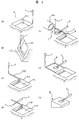
これに対して、ウェーハを分断することなく試料作製できる方法がある。この方法は、特開平05−52721号公報に開示されている。この方法は、図2の(a)に示すように、まず、試料2の表面に対しFIB1が直角に照射するように試料2の姿勢を保ち、試料上でFIB1を矩形に走査させ、試料表面に所要の深さの角穴101を形成する。次に、図2(b)に示すように、試料2を傾斜させ、底穴102を形成する。試料2の傾斜角の変更は、試料ステージ(図示せず)によって行われる。次に、試料2の姿勢を変更し、図2(c)に示すように、試料2の表面がFIB1に対して再び垂直になるように試料2を設置し、切り欠き溝103を形成する。マニピュレータ(図示せず)を駆動し、図2(d)に示すように、マニピュレータ先端のプローブ3の先端を、試料2を分離する部分に接触させる。
【0010】
次に、図2(e)に示すように、ガスノズル104から堆積性ガス5を供給し、 FIB1をプローブ3の先端部を含む領域に局所的に照射し、イオンビームガスアシストデポジション膜(以下、デポ膜4と略す。)を形成する。接触状態にある試料2の分離部分とプローブ3の先端はデポ膜4で接続される。図2(f)に示すように、FIB1で残りの部分を切り欠き加工し、試料2から分離試料であるマイクロサンプル6を切り出す。切り出された分離試料6は、図2(g)に示すように、接続されたプローブ3で支持された状態になる。このマイクロサンプル6を、FIB1で加工し、観察しようとする領域をウォール加工するとTEM試料(図示せず)となる。
【0011】
以上のように、本方法はウェーハなどの試料から所望の解析領域を含む微小試料片を、FIB加工と微小試料の搬送手段を駆使して分離する方法である。この方法で分離した微小試料を各種解析装置に導入することで解析することができる。
【0012】
この試料の分離方法を用いてウェーハを分断することなく、試料から検査用の微小試料を取り出し、ウェーハは次のプロセスに戻す手法については、特開2000−156393号公報に開示されている。この手法によれば、ウェーハの分断によって失われる半導体デバイスはなくなり、トータルの半導体デバイスの製造コストを低減することができる。
【0013】
上述のような電子部品の製造に関しては、ウェーハを次のプロセスに戻す場合に、マイクロサンプルを取り出した後の加工穴の処理が必要となる。すなわち、加工穴を処理しなかった場合には、以下のような問題が生じる。
【0014】
(1)加工穴の端が欠けて汚染源になる。(2)スピンコート、研磨時等にウェーハ不均一形状を誘発する。(3)穴がゴミの溜まり場となる。例えば、マイクロサンプルを取り出した後にCMP(Chemical&Mechanical Polishing)プロセスを行う場合、CMP砥粒が加工穴に入り洗浄しても取りきれず、CMP以降の工程のプロセスでCMP砥粒が穴から飛び出して異物になったり、デバイス特性を変動させるような不純物汚染となったりする。
【0015】
FIB加工した後でウェーハをプロセスラインに戻すという技術の関連では、特開平6−260129号公報に開示されている。この方法では、イオン源としてガリウムを用いた集束イオンビームを照射した試料をプロセスに戻すために、試料の特性に顕著な影響を及ぼさない気体元素のイオンビームを用いて、ガリウムの打ち込まれた部分を除去するか、前記気体イオンビーム、もしくはエネルギビームを用いてガリウムの打ち込まれた部分を被覆するように有機金属膜を析出する方法が開示されている。すなわち、アルゴン、酸素イオン、酸素ラジカルのいずれかを用いて加工観察領域をクリーン化し化合物を堆積させた後再び製造工程に戻すことが開示されている。
【0016】
しかし、この装置では、Ga汚染に関しては考慮されているものの、加工後の穴の処理については考慮されていなかった。
【0017】
また、断面検査後にウェーハをプロセスラインに戻すという技術の関連では、特開平10−116872号公報に開示されている。この方法では、半導体デバイスのプロセス途中で、ウェーハを断面検査した後に、断面加工穴をエネルギビーム誘起CVD(Chemical Vapour Deposition、なお、従来例ではCVDという技術語を用いているが、ここでは、ガスアシストデポジションを同義語として用いる。)により絶縁体や導電膜を埋めこんだり、あるいは液体材料を塗布し、エネルギビームを照射することによって所望の膜質で穴埋めして、再び製造プロセスラインにウェーハを戻して製造を続行する方法が開示されている。特に、ウエーハを抜き取って断面検査を行い、ウエーハの検査部分をイオンビームで平坦化することが開示されている。
【0018】
また、国際公表特許WO99/17103号公報には、FIB加工後の穴の処理として、イオンビームで開口部を誘電体で覆うことのみが開示されている。
【0019】
【発明が解決しようとする課題】
しかし、FIB加工後の従来の穴埋め方法では、次のような課題が残されていた。
【0020】
まず、エネルギビーム誘起ガスアシストデポジションにより穴埋めを実施する場合には、ビーム種により各々次のような問題があった。
【0021】
すなわち、(1)液体材料を塗布し、エネルギビームを照射することによって膜を形成する場合には、膜が厚くなるとエネルギビームを照射する工程で膜にクラックが生じ、ウェーハを次のプロセスに戻すと、プロセス中にクラックのかけらが飛散し、不良原因となる懸念があった。これは、一般にマイクロサンプルを取り出した加工穴の深さは、浅くとも3から5マイクロメートルあり、一方、液体材料で一般に用いられる酸化膜材料がクラックなしで形成できる膜厚はせいぜい1から2マイクロメートルまでで、それ以上に厚く塗布された酸化膜は加熱の過程でクラックが生じるからである。(2)レーザビーム誘起ガスアシストデポジションでは、等方的に膜成長するため平坦に穴埋めすることが困難である。(3)アルゴンイオンビーム誘起ガスアシストデポジションでは、廉価なイオン照射系では、ビームサイズは50から500マイクロメートルが一般的であり、一方、加工穴の大きさは大きくとも20マイクロメートル程度であるため、加工穴のみに膜形成することが難しく加工穴周辺にも膜を形成し平坦な穴埋めが困難である。(4)電子ビーム誘起ガスアシストデポジションでは、一般にデポ速度が遅いため、実用的な時間、例えば10分以内に穴埋めすることが困難である。
【0022】
次に、(5)ガリウムFIB誘起ガスアシストデポジションでは、加工穴を狙ってデポ膜形成が可能であるが、デポ膜中にガリウムが取り込まれるという問題がある。さらに、FIB照射によるスパッタ作用によりFIB加工領域以外にも、ガリウムや試料の一部の破片が飛散する。これらのガリウム汚染が半導体デバイス製造にとっては不良発生原因となる可能性が高い。すなわち、これらの汚染をそのままにして、ウェーハを次のプロセスに戻すと、ガリウムが拡散し、正常に製造プロセスを経ていた半導体素子に侵入し、電気的特性不良やコンタクト不良を発生させるという問題がある。また、高速に穴を埋めるという観点では、電子ビーム誘起ガスアシストデポジションに比較すれば早いものの、やはり実用的な時間、例えば10分以内に穴埋めすることが困難である。これは、デポ膜の絶対量はFIB電流に比例して大きくすることができるため、穴埋め速度をより大きくするためには、FIB電流を大きくする。しかし、FIB電流を大きくすると、すなわち約1nA以上の高電流にすると、デポ膜形成効率が低下して、デポ量とスパッタ量が同程度になり、デポ膜の成長が止まってしまい高速の穴埋めはできなかった。
【0023】
このようなことから、半導体デバイス等の歩留向上のために、ウェーハを割断することなく途中の検査を実施するために、次のような技術が望まれていた。すなわち、マイクロサンプルを取り出した加工穴、あるいは、断面検査した後の加工穴を、平坦性良く、高速に埋め戻す技術。また、後のプロセスで問題が生じ無いように、異物が発生せず、またガリウム汚染が半導体デバイスの不良発生原因とならないような埋め戻し手法の確立や、それを、実現できる装置の開発が望まれていた。
【0024】
特に、検査後のウェーハを製造ラインに戻すという観点では、製造ラインに戻すまでの時間短縮が重要であり、すなわち穴埋めの高速化技術が望まれており、従来の方法はこの課題を解決できていなかった。例えば、FIB電流を大きくしても、すなわち約1nA以上の高電流にしても、デポ膜形成効率が低下することなく、デポ量が増大し高速の穴埋めが可能な技術が望まれていた。
【0025】
そこで、本発明の目的は、上述の問題点に鑑み、FIBを使ったサンプリング後の加工穴を高速に埋める技術を提供し、上記ウェーハを評価のために無駄に廃棄せず、かつ検査のための試料を取り出したウェーハをプロセスに戻しても不良を発生させない新たな検査・解析方法や電子部品製造方法、また、そのための加工・観察装置を提供することにある。
【0026】
【課題を解決するための手段】
上記目的を達成するために、本発明では、以下のようにすることによって達成される。
【0027】
(1)イオン銃と、前記イオン銃から放出するイオンビームを集束するレンズと、イオンビームを走査する偏向器と、該偏向器の制御装置と、該イオンビームを試料に照射して該試料からの2次粒子を検出するための検出器と、イオンビームガスアシストデポジション用ガスを試料近傍に供給するガス銃と、該試料を保持する試料台と、該試料台の位置を制御する試料位置制御装置を備える荷電粒子線装置によって、試料表面に存在する穴の中にイオンビームガスアシストデポジション膜を形成して前記穴を埋める方法において、荷電粒子を走査する領域を、穴の側壁の一部にイオンビームが照射され、一部には照射されないように制御して穴の中に荷電粒子ガスアシストデポジション膜を形成することを特徴とする穴埋め方法とする。
【0028】
本手法によると、FIBを使ったサンプリング後の加工穴を高速に埋める方法が提供される。
【0029】
(2)イオン銃と、前記イオン銃から放出するイオンビームを集束するレンズと、イオンビームを走査する偏向器と、該偏向器の制御装置と、該イオンビームを試料に照射して該試料からの2次粒子を検出するための検出器と、イオンビームガスアシストデポジション用ガスを試料近傍に供給するガス銃と、該試料を保持する試料台と、該試料台の位置を制御する試料位置制御装置を備えるイオンビーム装置によって、試料表面に存在する穴の中にイオンビームガスアシストデポジション膜を形成して前記穴を埋める方法において、イオンビームを走査する領域を、穴の開口領域と概略同じく設定して、穴の位置に対して移動を伴うように走査領域を制御して穴の中にイオンビームガスアシストデポジション膜を形成することを特徴とする穴埋め方法とする。
【0030】
本手法によると、FIBを使ったサンプリング後の加工穴を高速に埋める方法が提供され、特に、イオンビーム走査領域の設定が容易な穴埋め方法が提供される。
【0031】
(3)イオン銃と、前記イオン銃から放出するイオンビームを集束するレンズと、イオンビームを走査する偏向器と、該偏向器の制御装置と、該イオンビームを試料に照射して該試料からの2次粒子を検出するための検出器と、イオンビームガスアシストデポジション用ガスを試料近傍に供給するガス銃と、該試料を保持する試料台と、該試料台の位置を制御する試料位置制御装置を備えるイオンビーム装置によって、試料表面に存在する穴の中にイオンビームガスアシストデポジション膜を形成して前記穴を埋める方法において、イオンビームを走査する領域を、少なくとも穴の側壁の一部から遠ざかるように移動させるように制御して穴の中にイオンビームガスアシストデポジション膜を形成することを特徴とする穴埋め方法とする。
【0032】
本手法によると、FIBを使ったサンプリング後の加工穴を高速に埋める方法が提供される。
【0033】
(4)イオン銃と、前記イオン銃から放出するイオンビームを集束するレンズと、イオンビームを走査する偏向器と、該偏向器の制御装置と、該イオンビームを試料に照射して該試料からの2次粒子を検出するための検出器と、イオンビームガスアシストデポジション用ガスを試料近傍に供給するガス銃と、該試料を保持する試料台と、該試料台の位置を制御する試料位置制御装置を備えるイオンビーム装置によって、試料表面に存在する穴の中にイオンビームガスアシストデポジション膜を形成して前記穴を埋める方法において、イオンビームを走査する領域を、穴の側壁の一部にイオンビームが照射され、一部には照射されないように制御し、かつ穴埋め時間経過と共に走査する領域を継続的に縮小するように制御して穴の中にイオンビームガスアシストデポジション膜を形成することを特徴とする穴埋め方法。
【0034】
本手法によると、FIBを使ったサンプリング後の加工穴を高速に埋める方法が提供され、特に、イオンビームが穴以外の領域を照射することがないため平坦性が良い穴埋め方法が提供される。
【0035】
(5)イオン銃と、前記イオン銃から放出するイオンビームを集束するレンズと、イオンビームを走査する偏向器と、該偏向器の制御装置と、該イオンビームを試料に照射して該試料からの2次粒子を検出するための検出器と、イオンビームガスアシストデポジション用ガスを試料近傍に供給するガス銃と、該試料を保持する試料台と、該試料台の位置を制御する試料位置制御装置を備えるイオンビーム装置によって、試料表面に存在する穴の中にイオンビームガスアシストデポジション膜を形成して前記穴を埋める方法において、穴の開口部の径もしくは長辺に対して穴の深さが深い穴の中に、イオンビーム電流を1nA以上照射して、イオンビームを走査する領域を、穴の開口領域と概略同じく設定して、穴の位置に対して移動を伴うように走査領域を制御して穴の中にイオンビームガスアシストデポジション膜を形成することを特徴とする穴埋め方法。
【0036】
本手法によると、FIBを使ったサンプリング後の加工穴を高速に埋める方法が提供され、特に、イオンビーム電流が多いことから高速で、かつイオンビーム走査領域の設定が容易な穴埋め方法が提供される。
【0037】
(6)イオン銃と、前記イオン銃から放出するイオンビームを集束するレンズと、イオンビームを走査する偏向器と、該偏向器の制御装置と、該イオンビームを試料に照射して該試料からの2次粒子を検出するための検出器と、イオンビームガスアシストデポジション用ガスを試料近傍に供給するガス銃と、該試料を保持する試料台と、該試料台の位置を制御する試料位置制御装置を備えるイオンビーム装置によって、試料表面に存在する穴の中にイオンビームガスアシストデポジション膜を形成して前記穴を埋める方法において、イオンビーム照射による二次電子像の輝度変化をモニタして走査領域を移動量および移動時間を管理して、穴の中にイオンビームガスアシストデポジション膜を形成することを特徴とする穴埋め方法とする。
【0038】
本手法によると、FIBを使ったサンプリング後の加工穴を高速に埋める方法が提供され、特に、イオンビーム走査領域の移動が効率的な穴埋め方法が提供される。
【0039】
(7)基板に、イオンビームを照射して、基板表面を加工し、加工部を検査あるいは解析する、もしくはイオンビーム照射を用いる加工方法により基板の一部を分離して、分離したマイクロサンプルを検査・解析する基板の検査・解析方法において、基板上でイオンビーム照射によって形成された加工穴をエネルギ誘起ガスアシストデポジション膜により埋めこみ、次にガスアシストデポジション膜上に液体材料を塗布することを特徴とする基板の検査・解析方法とする。
【0040】
本手法によると、基板を評価のために無駄に廃棄せず、かつ検査のための試料を取り出したウェーハをプロセスに戻しても不良を発生させない新たな検査・解析方法が提供され、特に、加工穴を、平坦性良く埋め戻すことができ、かつ異物が発生しにくく、イオン種による汚染の影響も低減できる。
【0041】
(8)基板に、ガリウム集束イオンビームを照射して、基板表面を加工し、加工部を検査あるいは解析する、もしくはガリウム集束イオンビーム照射を用いる加工方法により基板の一部を分離して、分離したマイクロサンプルを検査・解析する基板の検査・解析方法において、基板上でガリウム集束イオンビーム照射によって形成された加工穴にガリウム集束イオンビーム誘起ガスアシストデポジションにより埋めこみ、次にガスアシストデポジション膜上に液体材料を塗布し、次に液体材料を個化した後、基板表面をガリウム除去洗浄することを特徴とする基板の検査・解析方法とする。
【0042】
本手法によると、基板を評価のために無駄に廃棄せず、かつ検査のための試料を取り出したウェーハをプロセスに戻しても不良を発生させない新たな検査・解析方法が提供され、特に、加工穴を、平坦性良く埋め戻すことができ、かつ異物が発生しにくく、加工穴周辺も含めて、イオン種による汚染の影響が低減できる。
【0043】
(9)基板に、イオンビームを照射して、基板表面を加工し、加工部を検査あるいは解析する、もしくはイオンビーム照射を用いる加工方法により基板の一部を分離して、分離したマイクロサンプルを検査・解析する基板の検査・解析方法において、基板上でイオンビーム照射によって形成された加工穴にブロック状の部材を挿入することを特徴とする基板の検査・解析方法とする。
【0044】
本手法によると、基板を評価のために無駄に廃棄せず、かつ検査のための試料を取り出したウェーハをプロセスに戻しても不良を発生させない新たな検査・解析方法が提供され、特に、加工穴を、スループット高く埋め戻すことができる。
【0045】
(10)基板に、集束イオンビームを照射して、基板表面を加工し、加工部を検査あるいは解析する、もしくは集束イオンビーム照射を用いる加工方法により基板の一部を分離して、分離したマイクロサンプルを検査・解析する基板の検査・解析方法において、基板上でイオンビーム照射によって形成された加工穴を集束イオンビーム誘起ガスアシストデポジション膜により埋めこみ、次に該ガスアシストデポジション膜上を気体元素種イオンビーム誘起ガスアシストデポジション膜で覆うことを特徴とする基板の検査・解析方法とする。
【0046】
本手法によると、基板を評価のために無駄に廃棄せず、かつ検査のための試料を取り出したウェーハをプロセスに戻しても不良を発生させない新たな検査・解析方法が提供され、特に、加工穴を、平坦性良く埋め戻すことができ、かつ異物が発生しにくく、イオン種による汚染の影響も低減できる。
【0047】
(11)基板に、集束イオンビームを照射して、基板表面を加工し、加工部を検査あるいは解析する、もしくは集束イオンビーム照射を用いる加工方法により基板の一部を分離して、分離したマイクロサンプルを検査・解析する基板の検査・解析方法において、基板上でイオンビーム照射によって形成された加工穴を集束イオンビーム誘起ガスアシストデポジション膜により埋めこみ、次に該ガスアシストデポジション膜上をレーザビーム誘起ガスアシストデポジション膜で覆うことを特徴とする基板の検査・解析方法とする。
【0048】
本手法によると、基板を評価のために無駄に廃棄せず、かつ検査のための試料を取り出したウェーハをプロセスに戻しても不良を発生させない新たな検査・解析方法が提供され、特に、加工穴を、平坦性良く、スループット高く埋め戻すことができ、かつ異物が発生しにくく、イオン種による汚染の影響も低減できる。
【0049】
(12)基板に回路パターンを製造するプロセスの任意の加工工程後に、前記基板にイオンビームを照射して、基板表面を加工し、加工部を検査あるいは解析する工程、もしくは前記加工工程の後に、少なくともイオンビーム照射を用いて前記基板の一部を分離する工程を有し、その後、基板上でイオンビーム照射によって形成された加工穴をエネルギ誘起ガスアシストデポジションにより埋めこみ、次にガスアシストデポジション膜上に液体材料を塗布する工程を経た後、回路パターンを製造する前記プロセスに前記基板を戻して第二の加工をすることを特徴とする電子部品製造方法とする。
【0050】
本手法によると、基板を評価のために無駄に廃棄せず、かつ検査のための試料を取り出したウェーハをプロセスに戻しても不良を発生させない新たな電子部品製造方法が提供される。
【0051】
(13)基板に回路パターンを製造するプロセスの任意の加工工程後に、前記基板にイオンビームを照射して、基板表面を加工し、加工部を検査あるいは解析する工程、もしくは前記加工工程の後に、少なくともイオンビーム照射を用いて前記基板の一部を分離する工程を有し、その後、基板上でイオンビーム照射によって形成された加工穴をエネルギ誘起ガスアシストデポジションにより埋めこみ、次に該ガスアシストデポジション膜上を気体元素種イオンビームもしくはレーザビーム誘起ガスアシストデポジション膜で覆う工程を経た後、回路パターンを製造する前記プロセスに前記基板を戻して第二の加工をすることを特徴とする電子部品製造方法とする。
【0052】
本手法によると、基板を評価のために無駄に廃棄せず、かつ検査のための試料を取り出したウェーハをプロセスに戻しても不良を発生させない新たな電子部品製造方法が提供される。
【0053】
(14)基板に、集束イオンビームを照射して、基板表面を加工し、加工部を観察する、もしくは集束イオンビーム照射を用いる加工方法により基板の一部を分離して検査・解析用のマイクロサンプルを作製する基板の加工・観察装置において、基板上でイオンビーム照射によって形成された加工穴を集束イオンビーム誘起ガスアシストデポジション膜により埋めこみ、次に該ガスアシストデポジション膜上を気体元素種イオンビームもしくはレーザビーム誘起ガスアシストデポジション膜で覆う機能を有することを特徴とする基板の加工・観察装置とする。
【0054】
本装置によると、基板を評価のために無駄に廃棄せず、かつ検査のための試料を取り出したウェーハをプロセスに戻しても不良を発生させない新たな検査・解析方法のための試料作製が可能な基板の加工・観察装置が提供され、特に、加工穴を、平坦性良く、スループット高く埋め戻すことができ、かつ異物が発生しにくく、イオン種による汚染の影響も低減できる基板の加工・観察装置が提供される。
【0055】
(15)基板に、集束イオンビームを照射して、基板表面を加工し、加工部を観察する、もしくは集束イオンビーム照射を用いる加工方法により基板の一部を分離して検査・解析用のマイクロサンプルを作製する基板の加工・観察装置において、基板上でイオンビーム照射によって形成された加工穴を集束イオンビーム誘起ガスアシストデポジション膜により埋めこみ、次に該ガスアシストデポジション膜上を気体元素種イオンビームもしくはレーザビーム誘起ガスアシストデポジション膜で覆う機能を有し、集束イオンビーム照射軸と、気体元素種イオンビーム照射軸もしくはレーザビーム照射軸がオフセットされていることを特徴とする基板の加工・観察装置とする。
【0056】
本装置によると、基板を評価のために無駄に廃棄せず、かつ検査のための試料を取り出したウェーハをプロセスに戻しても不良を発生させない新たな検査・解析方法のための試料作製が可能な基板の加工・観察装置が提供され、特に、加工穴を、平坦性良く、スループット高く埋め戻すことができ、かつ異物が発生しにくく、イオン種による汚染の影響も低減できる基板の加工・観察装置が提供される。
【0057】
また、上記(1)から(15)のいずれかにおいて、上記試料はシリコン半導体ウェーハ、エピタキシャル成長シリコンウェーハ、基板に形成されたシリン薄膜を有するウェーハ、化合物半導体ウェーハ、磁気ヘッド集積ウェーハのうちのいずれかである。また、上記電子部品は、シリコン半導体デバイス、化合物半導体デバイス、磁気記録再生用ヘッド、光磁気記録再生用ヘッドのうちのいずれかである。また、上記検査は、透過型電子顕微鏡、走査型透過電子顕微鏡、走査型電子顕微鏡もしくは走査型プローブ顕微鏡のうちの少なくともいずれかを用いる。また、上記解析は、電子ビーム、イオンビーム、X線の少なくともいずれかを用いて元素分析し、予め定めた基準の元素分布または元素濃度、不純物分布、不純物濃度のうち少なくともいずれと比較して良不良を判断する。また、上記解析は、予め定めた箇所について予め定めた基準の形状、寸法、元素分布、元素濃度、不純物分布、不純物濃度のうち少なくともいずれかを外れた原因を解明する。また、上記モニタまたは検査または解析のうちの少なくともいずれかを行なう工程において得たデータは、少なくとも計算処理機に保存する。
【0058】
【発明の実施の形態】
本発明によるFIBを使ったサンプリング後の加工穴を高速に埋める方法の実施例は、ある加工プロセス後において試料の基板表面を含む一部をFIBにより摘出し、または断面を形成し、上記基板表面を含む一部または断面に対して上記加工プロセスでの加工の進捗を検査または解析のうちの少なくともいずれかの方法、および上記摘出もしくは断面形成後の加工穴を高速に埋め戻す方法にある。
【0059】
また、さらに本発明による電子部品製造方法の実施例は、試料に複数の加工プロセスを施して電子部品を形成する電子部品製造方法において、上記基板表面を含む一部または断面に対して上記加工プロセスでの加工の進捗を検査または解析のうちの少なくともいずれかを行なう工程と、上記摘出または断面形成後の加工穴を埋め戻す工程とを含み、基板を更に加工プロセスへ戻し回路パターンを製造する方法にある。
【0060】
(実施例1)
本発明による検査・解析方法を含む電子部品製造方法の基本的な流れをウェーハの流れを、図1を用いて説明する。
【0061】
まず複数のウェーハからなるロット13が任意のN番目のプロセス11に投入される。次に、複数のウェーハのうち検査用ウェーハ14を選別し、残されたウェーハは待機する。選別した検査用ウェーハ14は、まず検査電子顕微鏡15に導入される。ここで異常が発見された場合には、その位置がアドレスとして記録され、その情報が試料加工・観察装置17に送られる。この試料加工・観察装置17で検査用ウェーハ14から検査すべき箇所を含むマイクロサンプル6を、ガリウムFIB1とマニピュレータ先端に取り付けたプローブ3、およびデポガスW(CO)6によって作製したデポ膜等を用いて摘出する。
【0062】
マイクロサンプル6を摘出された検査用ウェーハ14は、再び上記残されたロット13に組み込まれ、次のN+1番目のプロセス12に投入される。ここで、マイクロサンプル6は解析装置18に送り、予め定められた検査項目について解析する。このように、N番目のプロセスからN+1番目プロセスに至る間に、解析用のマイクロサンプル6が摘出されることが大きな特徴である。
【0063】
また、検査によってマイクロサンプル6を摘出した加工領域を含む半導体デバイスは、N+1番目以降のプロセスは無効となり製品となることはないが、ウェーハ枚数は減少することはない。すなわち、N番目のプロセスに投入するウェーハとN+1番目のプロセスに投入するウェーハ数は同じであり、マイクロサンプル6が取り出された領域以外で製造された半導体デバイスは良品であれば製品として製造数に貢献する。
【0064】
しかし、これだけでは、マイクロサンプルを取り出した後の加工穴がウェーハを次のプロセスに戻す場合の問題となる。そこで、上記マイクロサンプルを取り出した後の加工穴を埋め戻す。
【0065】
まず、加工・観察装置17で、ウェーハ上でイオンビーム照射によって形成された加工穴をFIB誘起ガスアシストデポジション膜により埋めこみ、次にガスアシストデポジション膜上に液体材料を塗布する方法について説明する。
【0066】
本手法のフローを図3に示す。図3(a)に示すように、ガリウムFIB1を用いたマイクロサンプル6作製のための加工動作については従来の方法と同じであるが後で詳しく説明する。次に、図3(b)に示すように、試料ウェーハ38は、次のプロセスに投入されるが、ウェーハ上でFIB照射によって形成された加工穴をFIBガスアシストデポジションで埋める。この詳しい動作についても、図6を用いて後述する。
【0067】
次に、図3(c)に示すように、かかるウェーハは加工・観察装置17から取りだされ、液体材料塗布装置19に導入され、FIB照射加工領域を覆うように、例えば直径1mm領域に液体材料302をピペット301から射出して塗布する。次に塗布した液体材料からの保護膜形成は、加熱手段により焼成される。この方法についても後で詳しく説明する。次に、図3(d)に示すように、洗浄装置20により、例えばブラシ304と薬液を用いたいわゆるブラシ洗浄により、ウェーハを洗浄し液体塗布領域外のガリウム汚染を除去する。
【0068】
次に、本発明による一実施例である手法に使用する加工・観察装置の概略構成図を、図4に示す。
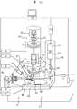
【0069】
加工・観察装置17は、真空容器41を有しており、真空容器内には、ガリウムを放出する液体金属イオン源32、ビーム制限アパーチャ33、イオンビーム走査電極34、およびイオンビームレンズ31などから構成されるFIB照射光学系35、FIB照射によって試料から放出する二次電子や二次イオンを検出する二次粒子検出器36、イオンビーム照射領域にデポ膜を形成するための元材料ガスを供給するデポガス源37、マニピュレータ43先端に取り付けたプローブ3、半導体ウェーハや半導体チップなどの試料ウェーハ38を載置する試料ステージ39、試料ウェーハの一部を摘出した微小な摘出試料を固定する試料ホルダ40などが配置されている。そして、主に電気回路や演算装置からなるステージ制御装置61、マニピュレータ制御装置62、二次電子検出器の増幅器63、デポガス源制御装置64、FIB制御装置65、および計算処理装置74、などが配置される。
【0070】
次に、本加工・観察装置の動作について説明する。まず、液体金属イオン源32から放出したイオンをビーム制限アパーチャ33、イオンビームレンズ31を通して試料ウェーハ38に照射する。FIB1は試料上で直径数ナノメートルから1マイクロメートル程度に細束化される。FIB1を試料ウェーハ38に照射するとスパッタリング現象により試料表面の構成原子が真空中に放出される。したがってイオンビーム走査電極34を用いてFIB1を走査させることで、マイクロメートルからサブマイクロメートルレベルの加工ができることになる。
【0071】
また、デポジションガスを試料室中に導入しながらFIB1を試料ウェーハ38に照射することによって、デポ膜を形成することができる。このように、FIB1によるスパッタリングあるいはデポジションを巧みにつかって試料ウェーハ38を加工することができる。FIB1照射によって形成するデポ膜は、プローブ3の先端にある接触部と試料を接続したり、摘出試料を試料ホルダ40に固定するために使用する。また、FIB1を走査して、試料から放出される二次電子や二次イオンを二次粒子検出器36で検出して、その強度を画像の輝度に変換することによって試料ウェーハ38やプローブ3などを観察することができる。
【0072】
次に、ガリウムFIB1を用いたマイクロサンプル6作製のための加工動作については従来の方法と同じであるが、図5を用いて説明する。
【0073】
この方法は、図5の(a)〜(j)に示すように、まず始めに、FIB1を照射し目標位置識別のためのマーク403、404を形成し、その後その両外側に矩形穴401、402を試料2に形成する(図5(a))。次に、FIB1により矩形溝406を形成する(図5(b))。次に、試料ステージを傾けてFIB1を試料表面に斜めから照射することにより、斜溝408を形成し、試料4と一部の支持部405のみで接続された摘出試料407を形成する(図5(c))。試料台傾斜を戻し、プローブ3を、プローブ制御装置により制御し、摘出試料407の一部に接触させる。この摘出試料の支持部405は、後程、FIBにより切断するわけであるが、プローブドリフト等を考慮した場合、短時間で切断することが望ましいため、支持部体積は小さくする必要がある。このため、プローブ3の接触により支持部405が破壊される恐れがあるため、上記プローブ制御法を使用して損傷をできるだけ抑えて接触させる。接触させたプローブ7と摘出試料407を、デポ膜409を用いて固定する(図5(d))。
【0074】
次に、支持部405をFIB1で切断する(図5(e))。こうして、摘出試料407を切り出し、プローブ3をプローブ駆動装置によって上昇させ摘出する(図5(f))。次に、この切り出された摘出試料407を摘出試料ホルダに形成された溝411への接触を行う(図5(g))。このときの接触は摘出試料407が破壊されたりデポ膜409部で摘出試料407が外れて消滅してしまわないように充分小さな速度で接触させる必要がある。こうして接触させた後、デポ膜412を用いて両者を固定する(図5(h))。固定後、プローブ3接続部にFIBを照射し、スパッタ加工を行い、プローブを摘出試料407から分離する(図5(i))。TEM試料とする場合には最後に、再度、FIB1を照射して、最終的に観察領域410を厚さ100nm以下程度に薄く仕上げ加工を施す(図5(j))。
【0075】
次に、マイクロサンプル6摘出よって形成された加工穴をFIBガスアシストデポジションで埋める動作について、図6を用いて説明する。
【0076】
まず、ガスノズル104から堆積性ガス5を供給し、FIB1の走査領域1002を、穴の開口領域と同じく設定して、FIB1を加工穴1001内のみに照射する。すると加工穴1001内の側壁、底面にはデポ膜が形成される。次に、走査領域1002は、図6(a)の矢印が示すように、4つの壁の内、2つの壁から遠ざかる方向にFIBを移動させて、走査領域の一部が加工穴と重なるようにする。すなわち、穴の側壁の一部にFIBが照射され、一部には照射されない状態にする。具体的には、4つの側壁の内、2つの壁にはFIBが照射され、他の2つの壁に形成ざれた側壁すなわちデポ膜にはFIBが照射されなくなる。ここではFIBが照射されている側壁から放出されるスパッタ粒子が、FIBが照射されなくなった2つの側壁に再付着して、側壁方向のデポジションが加速されることになる。
【0077】
次に、走査領域1002は順次移動させて、最後には走査領域が加工穴と重ならない状態で終了する。すなわち、穴埋めは、図6(b)に模式的に示したように、主に穴の側壁方向からのデポ膜成長によって行われる。ここで、実際には底面にもデポ膜は形成されるが、わかりやすくするため、図6(b)では省略した。なお、デポ膜4が堆積してほぼ加工穴が満たされたら堆積性ガス5供給を停止する。
【0078】
従来は、FIB1の走査領域は、穴の開口領域と同じく設定して、移動させることなくFIB1は加工穴1001内を照射し続け、デポ膜の成長は、図7(b)に模式的に示したように、主に底面からのデポ膜成長によって行われた。ここで、高速に穴を埋めるためには、デポ膜の絶対量がFIB電流に比例して大きくなるため、穴埋め速度をより大きくするためには、FIB電流を大きくする方が有利である。しかし、従来の方法ではFIB電流を大きくすると、すなわち約1nA以上の高電流にすると、デポ効率が低下しデポ量とスパッタ量が同程度になり、デポ膜の成長が止まってしまい高速の穴埋めはできなかった。しかし本願の手法では、イオンビーム電流を1nA以上照射しても、一旦成長した側壁にはFIBが照射されず、反対側壁からのスパッタ粒子の再付着により、高速の穴埋めが実現する。
【0079】
また、本実施例では、走査領域1002は穴を横切るように移動させたが、走査領域を図8に示すような方法で移動する方法も良い。図8では、○印がFIBの照射点を示しており、図8の(a)から(b)、(c)、(d)にしたがって、走査領域を1003から、1004、1005、1006に順次示したように、4つの壁の内2つの壁から遠ざけるように移動させる。このようにすると、走査領域1003の時に壁に成長したデポ膜に、走査領域を1004にした時にはFIBが照射されず、反対側壁からのスパッタ粒子の再付着が加わり、2つの壁からのデポ膜成長が継続することになり、高速の穴埋めが実現する。
【0080】
また、図9に示すような、次のような方法も良い。すなわち、FIBを走査する領域を、FIB照射密度を概略一定にして、穴の位置に対して継続的に縮小するように制御して穴の中にデポ膜を形成する。図9では、○印がFIBの照射点を示しており、図9の(a)に示す1003が最初の走査領域を示し、(b)に示す1004は縮小された走査領域を示しているが、1004に示す照射領域は、仮想の照射領域を1003として他の条件は概略一定にする。そして1004の外側にFIBが走査される時間にはFIBは試料に照射されないようにする。次に、(c)に示す走査領域が1005、および(d)に示す1006と縮小された場合にも同様である。こうすれば、デポ膜の成長は2つの壁から進み、より効率的に、すなわち高速に穴埋めができる。
【0081】
ただし、単純に走査領域を縮小すると、FIBの照射電流密度が実行的に増大し、穴埋め条件が変化するため、穴埋め制御が困難になる。したがって、走査領域を縮小するときには、設定する仮想の走査領域は一定にして、縮小で照射しない領域ではFIBが試料に照射されないように制御すれば、実効的な照射電流密度は一定にして走査領域を縮小でき穴埋め制御が可能になる。このようにすると、各々の走査領域で実行されるFIB照射時間を同じくすることができる。
【0082】
以上のような穴埋め方法が、特に活用できるのは、穴の開口部の径もしくは長辺に対して穴の深さが深い穴、いわゆる深い穴である。これは穴の底面に比較して、側面の面積が大きくなり、主に側壁からデポ膜を成長させる本手法がより効率的になるためである。
【0083】
また、この穴埋め方法では、FIB1の走査によって発生した二次電子の強度によって形成される二次電子像において、穴埋め開始後に壁周辺にデポ膜の成長に合わせて二次電子像の輝度が変化していく。この変化は側壁からのデポ膜の成長が平衡状態になった時点でほぼ停止する。したがって、効率良く走査領域を移動させるためには、この輝度変化が終了するタイミングで、かつ輝度変化する領域分を走査領域の移動させれば、ロスが無く効率良く穴埋めができることになる。このような設定を予めプログラミングしておけば、自動的に穴埋めが終了する。これはイオンビーム照射密度を概略一定にして、穴の位置に対して継続的に縮小するように制御する手法についても有効である。
【0084】
次に、ウェーハを加工・観察装置17から取りだし、液体材料塗布装置19に導入してFIB照射加工領域を覆うように液体材料を塗布する手法について述べる。
【0085】
液体材料としては、各種錯体溶液(例えば、スピンオングラス(略してSOG)と称される酸化ケイ素系被膜形成用塗布液、エポキシ系樹脂溶液、あるいはポリイミド前駆体溶液等が適用可能である。塗布は、微細ピペットを用いて行うことができる。塗布した液体材料から固体の保護膜への形成は、各種雰囲気炉、ホットプレート、レーザ、等の加熱手段を用いた焼成、紫外線ランプや紫外線レーザを照射する紫外線照射手段を用いた光硬化などで行う。焼成後は、洗浄装置20により、ウェーハを洗浄し液体塗布領域外のガリウム汚染を除去する。
【0086】
なお、本実施例では、加熱して形成した膜厚は約0.5マイクロメートル以下とした。これにより、従来、少なくとも数マイクロメートルの深さである穴の埋めもどしを液体材料のみで行っていたときに生じていたクラックの発生は大幅に低減できる。また、穴埋めの大半はFIBによって悪くても1μm以下の位置精度で行っているので、従来のアルゴンイオンビーム照射デポによる穴埋めのように加工穴から少なくとも数マイクロメートル周辺まで盛りあがるという問題も生じない。
【0087】
また、FIB照射した領域が酸化膜で覆われているので、ガリウムが後のプロセスで真空中に蒸発し、これが他の半導体素子に侵入し、電気的特性不良やコンタクト不良を発生させるという可能性も大幅に下がる。また、FIB照射のみによる穴埋めでは、ウェーハ表面と同じ高さに平坦に埋めることが難しく、約1マイクロメートル以下で凹凸が生じる場合が多い。しかし、この方法ではさらに液体材料を塗布するため凹凸が緩和され、より平坦な穴埋めが達成される。
【0088】
以上の本実施例によると、FIBを使ったサンプリング後の加工穴を高速に埋める方法が提供され、さらに、ウェーハを評価のために無駄に廃棄せず、かつ検査のための試料を取り出したウェーハをプロセスに戻しても不良を発生させない新たな検査・解析方法のための試料作製が可能なウェーハの加工・観察装置が提供され、かつ異物が発生しにくく、イオン種による汚染の影響も低減できるウェーハの加工・観察装置が提供される。
【0089】
(実施例2)
本発明の他の実施例に用いる、第2のイオンビーム照射装置を備えた加工・観察装置の概略構成を、図10に示す。
【0090】
本加工・観察装置17は、真空容器41を有しており、真空容器内には、FIB照射光学系35、二次粒子検出器36、デポガス源37、プローブ3、試料ステージ39等の構成は、実施例1の加工・観察装置と同様である。本装置では、アルゴン、酸素、窒素等の気体元素種のガスイオンを放出するデュオプラズマトロン81、イオンビームレンズ82、ビーム制限アパーチャ83、イオンビーム走査電極84などから構成される第二のイオンビーム照射系を設置している。
【0091】
また、本装置を制御する装置として、ステージ制御装置61、マニピュレータ制御装置62、二次電子検出器の増幅器63、デポガス源制御装置64、FIB制御装置65の他にデュオプラズマトロン制御装置91、光学系制御装置92、イオン走査制御装置93、および計算処理装置74、などが配置される。なお、本装置では、FIB照射軸とアルゴンイオンビーム照射軸は、図10に示すようにオフセットされている。これにより、FIB照射系の付近の装置設計が容易になるという特長を持つ。
【0092】
FIB照射光学系35の動作は実施例1と同様で、ガリウムFIB1を用いたマイクロサンプル作製のための加工動作についても従来の方法と同じである。そして、本装置から摘出したマイクロサンプル6は検査装置によって解析される。
【0093】
しかし、これだけでは、マイクロサンプル6を取り出した後の加工穴がウェーハを次のプロセスに戻す場合の問題となる。そこで、上記マイクロサンプルを取り出した後の加工穴を埋め戻す。
【0094】
本実施例では、ウェーハ上でガリウムFIB1照射によって形成された加工穴をガリウムFIB1誘起ガスアシストデポジション膜により埋めこみ、次に、ビーム径が1ミリメートルオーダのブロードなアルゴンイオンビーム照射によるデポ膜により前記ガリウムFIB1誘起ガスアシストデポジション膜を覆う方法について説明する。
【0095】
本手法のフローを、図11(a)〜(d)に示す。(a)に示すように、ガリウムFIB1を用いたマイクロサンプル6作製のための加工動作については従来の方法と同じである。次に、(b)に示すように、試料ウェーハ38は、次のプロセスに投入されるが、ウェーハ上でイオンビーム照射によって形成された加工穴をガリウムFIB1誘起ガスアシストデポジション膜により埋めこむ。この動作については、実施例1で説明した方法と同じである。
【0096】
次に、(c)に示すように、かかるウェーハは加工・観察装置17から取りだされる。本装置では、FIB照射軸とアルゴンイオンビーム照射軸はオフセットされているため、FIB誘起ガスアシストデポジション領域をアルゴンイオンビーム照射軸の直下にするように、試料台を移動する。ここで、別のガスノズル105からシリコン酸化膜用の堆積性ガス106を供給し、FIB穴埋め領域をほぼ中心に含むように、ビーム径が1ミリメートルオーダのブロードなアルゴンイオンビーム85を照射し、厚さ約0.5マイクロメートルの膜を形成する。また、ここでは、FIB照射軸とアルゴンイオンビーム照射軸はオフセットされているため、シリコン酸化膜用の堆積性ガス106を供給動作で、堆積性ガス5が混入する危険性が少ないと言う特長をもつ。
次に、(d)に示すように、洗浄装置20により、例えばブラシ304と薬液を用いたいわゆるブラシ洗浄により、ウェーハを洗浄し液体塗布領域外のガリウム汚染を除去する。
【0097】
ここで、FIBデポ膜形成後のアルゴンイオンビーム照射誘起デポ膜形成動作を説明する。アルゴンイオビーム照射装置のイオン源はデュオプラズマトロン81で、ここではアルゴンイオンを照射する。イオンビーム85の加速電圧は5kVで、イオン電流は2マイクロアンペア、ビーム径は約1ミリメートルに調整した。またビーム偏向電極84によってウェーハ試料38の任意の場所を狙うことが可能で、ガリウムが照射されたFIB穴埋め領域を狙って照射することも可能となる。
【0098】
このためには、あらかじめ次の準備しておく。まず、アルゴンイオンビーム85をスポット状に集束して試料に照射する。次に、試料台移動の後、そのスポット状の照射痕をFIB1で走査して、二次電子を検出して、スポット状の照射痕を観察することで、アルゴンイオンビーム照射位置とFIB1照射位置関係を明らかにしておく。そして、この装置のイオンビーム走査制御装置93にはマイクロサンプル6の加工位置とガリウムFIB照射条件情報を記憶しており、この記憶情報から加工位置を呼び出し、アルゴンイオンビーム照射系を制御し、加工位置にアルゴンイオンビーム85を自動照射する。なお、これらの制御は、計算処理装置74によって統一して行われる。
【0099】
なお、本実施例では、アルゴンイオンビームを用いたが酸素や窒素でも良い。また、イオンビームの替わりにレーザビームを照射しても良い。レーザビームでは短時間にデポ膜を形成できるため、スループットを上げたり、広領域を一度に処理するのに適している。一方、イオンビームはレーザ装置に比べて、目標位置に精度よく照射することができる。
【0100】
なお、本装置では、アルゴンイオンビーム装置をFIBイオンビーム装置に組み込んでいるが上記のアルゴンイオンビーム照射装置と同等の性能を持つ第二のイオンビーム照射装置で除去作業を行ってもよい。この場合には、加工位置情報を、FIBイオンビーム装置からアルゴンイオンビーム照射装置に転送し、加工位置を自動的にアルゴンイオンビーム照射できるようにする。ただしこの場合には2台の装置のコストが必要であり、作業時間も長くなり、結果的にはデバイス製造にかかる経済的なコストが高くなる。
【0101】
以上に述べた手法では、穴埋めの大半はFIBによって位置精度良く行っているので、従来のアルゴンイオンビーム照射デポのみによる穴埋めのように加工穴周辺が盛りあがるという問題が生じない。また、FIB照射した領域が広く酸化膜で覆われているので、ガリウムが後のプロセスで拡散し、半導体素子に侵入し、電気的特性不良やコンタクト不良を発生させるという可能性も大幅に下がる。また、FIB照射のみによる穴埋めでは、ウェーハ表面と同じ高さに平坦に埋めることが難しく、約1マイクロメートル以下で凹凸が生じる場合が多い。しかし、この方法ではさらにデポ膜を広く薄く形成するるため,局所的な凹凸が緩和され、より平坦な穴埋めが達成される。
【0102】
本実施例によると、ウェーハを評価のために無駄に廃棄せず、かつ検査のための試料を取り出したウェーハをプロセスに戻しても不良を発生させない新たな検査・解析方法のための試料作製が可能なウェーハの加工・観察装置が提供され、特に、加工穴を、平坦性良く、スループット高く埋め戻すことができ、かつ異物が発生しにくく、イオン種による汚染の影響も低減できるウェーハの加工・観察装置が提供される。
【0103】
(実施例3)
本発明の更に他の実施例に用いる加工・観察装置の概略構成図を、図12に示す。
【0104】
加工・観察装置17は、真空容器41を有しており、真空容器内には、ガリウムを放出する液体金属イオン源32、ビーム制限アパーチャ33、イオンビーム走査電極34、およびイオンビームレンズ31などから構成されるFIB照射光学系35、FIB照射によって試料から放出する二次電子や二次イオンを検出する二次粒子検出器36、イオンビーム照射領域にデポ膜を形成するための元材料ガスを供給するデポガス源37、マニピュレータ42先端に取り付けたプローブ3、半導体ウェーハや半導体チップなどの試料ウェーハ38を載置する試料ステージ39、試料ウェーハの一部を摘出した微小な摘出試料を固定する試料ホルダ40などが配置されている。
【0105】
また、レーザ発生オシレータ51等から構成されるレーザ装置56、また、レーザ用光学レンズ55等が装着されている。これらのレーザ装置56、レーザ用光学レンズ55等は一つのコンポーネントとしてまとめられ真空容器に固定されている。
【0106】
その他に本装置を制御する装置として、主に電気回路や演算装置からなるステージ制御装置61、マニピュレータ制御装置62、二次電子検出器の増幅器63、デポガス源制御装置64、FIB制御装置65、レーザ反射鏡位置制御装置71、レーザ用光学レンズ制御装置72、レーザ制御装置73、および計算処理装置74、などが配置される。なお、本装置では、FIB照射軸とレーザビーム照射軸は、図12に示すようにオフセットされている。FIB照射位置からレーザビーム照射位置へはステージ移動により数マイクロメートルの精度で移動可能である。このオフセット機能により、FIB照射系の付近の装置設計が容易になるという特長を持つ。
【0107】
FIB照射光学系35の動作は、実施例1と同様で、ガリウムFIB1を用いたマイクロサンプル作製のための加工動作についても従来の方法と同じである。そして、本装置から摘出したマイクロサンプル6は検査装置によって解析される。
【0108】
次に、試料ウェーハ38は、次のプロセスに投入されるが、ウェーハ上でイオンビーム照射によって形成された加工穴をガリウムFIB1誘起ガスアシストデポジション膜により埋めこみむ動作についても実施例1と同様である。
【0109】
次に、本実施例では、レーザビーム照射によるデポ膜により前記ガリウムFIB1誘起ガスアシストデポジション膜を覆う。まず、本装置では、FIB照射軸とレーザビーム照射軸はオフセットされているため、FIB誘起ガスアシストデポジション領域をレーザビーム照射軸の直下にするように、試料台を移動する。
【0110】
ここで、FIBデポ膜形成後のレーザビーム照射誘起デポ膜形成動作を説明する。ここではレーザ発生装置としてYAGレーザを用いる。まず、レーザ発生装置56から放出されたレーザ光57は、レーザ用光学レンズ55を通してガリウムFIB1誘起ガスアシストデポジション膜にむけて、真空容器内に導かれる。ここで、別のガスノズル105からシリコン酸化膜用の堆積性ガス106を供給し、FIB穴埋め領域をほぼ中心に含むように、レーザビームを照射し、厚さ約0.2マイクロメートルの膜を形成する。
【0111】
また、あらかじめレーザビーム照射痕をFIB1で走査して、試料から放出される二次電子を二次粒子検出器36で検出して、レーザビーム照射痕を観察することで、レーザビーム照射領域とイオンビーム照射領域の位置関係を明らかにしておくと、例えば、シリコンウェーハに製造している微細半導体デバイスに対し、加工位置情報を元に、FIB穴埋め領域42にレーザ光57を自動照射することができる。なお、これらの制御は計算処理装置74によって統一して行われる。また、ここでは、FIB照射軸とレーザビーム照射軸はオフセットされているため、シリコン酸化膜用の堆積性ガス106を供給動作で、堆積性ガス5が混入する危険性が少ないと言う特長をもつ。
【0112】
本実施例によると、ウェーハを評価のために無駄に廃棄せず、かつ検査のための試料を取り出したウェーハをプロセスに戻しても不良を発生させない新たな検査・解析方法のための試料作製が可能なウェーハの加工・観察装置が提供され、特に、加工穴を、平坦性良く、スループット高く埋め戻すことができ、かつ異物が発生しにくく、イオン種による汚染の影響も低減できるウェーハの加工・観察装置が提供される。
【0113】
本発明による他の実施例として、イオンビーム照射によって形成された加工穴にブロック状の部材を挿入して穴埋めする手法について説明する。なお、本実施例で用いる装置は、図4に示す加工・観察装置17と同じである。
【0114】
FIB照射光学系35の動作は実施例1と同様で、ガリウムFIB1を用いたマイクロサンプル作製のための加工動作についても従来の方法と同じである。そして、本装置から摘出したマイクロサンプル6は検査装置によって解析される。
【0115】
次に、マイクロサンプル作製後のウェーハ上でイオンビーム照射によって形成された加工穴にブロック状の部材を挿入する方法について説明する。
【0116】
まず、加工穴を埋めるのに好適な寸法に加工されたブロックの部材を真空容器41内に予め導入しておき、マニピュレータ先端のプローブ3の稼動範囲内に設置しておく。このブッロクの部材としては、シリコンあるいは、シリコン酸化物などを微細に加工したものあるいは、アルミニウムあるいは銅などの金属を微細に加工したものでも良い。
【0117】
次に、マニピュレータを駆動し、マニピュレータ先端のプローブ3の先端を、ブロック状の部材の表面部分に接触させる。ガスノズル104から堆積性ガス5を供給し、 FIB1をプローブ3の先端部を含む領域に局所的に照射し、デポ膜4を形成する。接触状態にあるブロック状の部材とプローブ3の先端はデポ膜4で接続される。ブロック状の部材が設置台などに固定されている場合には FIB1で接続部分を切り欠き加工し、ブロック状の部材を切り出す。切り出されたブロック状の部材は、接続されたプローブ3で支持された状態になる。次に、マニピュレータを駆動しブロック状の部材を加工穴上方に移動させ、さらに下降移動させてブロック状の部材を加工穴に挿入する。
【0118】
次に、ガスノズル104から堆積性ガス5を供給し、 FIB1をブロック状の部材と加工穴との隙間を含む領域に局所的に照射し、デポ膜4を形成する。ブロック状の部材と加工穴との隙間の全てもしくはその一部ははデポ膜4で埋められる。次に、プローブ3にFIBを照射することによってプローブ3を切断する。ブロック状の部材接続されるウェーハなど試料から所望の解析領域を含む微小試料片を、FIB加工と微小試料の搬送手段を駆使して分離する方法である。この方法で分離した微小試料を各種解析装置に導入することで解析することができる。
【0119】
以上、本手法によると、ウェーハを評価のために無駄に廃棄せず、かつ検査のための試料を取り出したウェーハをプロセスに戻しても不良を発生させない新たな検査・解析方法が提供され、特に、加工穴を、スループット高く埋め戻すことができる。
【0120】
以上に述べた実施例では、加工・観察装置でマイクロサンプルを取り出す方法を採用した例を述べたが、加工・観察装置で、マイクロサンプルの形状を加工し、加工・観察装置からウェーハを取り出して、別の機構でマイクロサンプルを取り出してもよい。
【0121】
例えば、図13(a)に示すように、ウェーハ上に薄膜207を形成し目標位置の両側を階段状にFIB1で加工して断面試料薄膜207を作製し、図13(b)に示すようにFIB1で試料薄膜周辺を切り取り、試料薄膜207をウェーハから切断する。そして、加工・観察装置からウェーハを取りだし、大気中でガラス棒の静電気を利用して、試料薄膜207をウェーハからTEM試料ホルダ209に移動させる。
【0122】
このように、マイクロサンプルを装置内で取り出さなくとも、マイクロサンプルの外形のほとんどをイオンビームによって加工する装置も、本発明に示す加工・観察装置に含む。また、以上のようにウェーハから解析用のマイクロサンプルを取り出す加工・観察装置ばかりでなく、ウェーハにFIBにより穴加工して、FIBもしくは同装置に取りつられた電子ビーム照射装置から放出された電子ビームにより断面部などデバイス内部を観察して、デバイス解析をする加工・観察装置も、本発明に示す加工・観察装置に含む。
【0123】
以上詳述したように、本発明によれば、FIBを使ったサンプリング後の加工穴を高速に埋める方法が実現でき、さらに、ウェーハを評価のために無駄に廃棄せず、かつ検査のための試料を取り出したウェーハをプロセスに戻しても不良を発生させない新たな検査・解析方法が実現され、特に、加工穴を、平坦性良く、スループット高く埋め戻すことができ、かつ異物が発生しにくく、イオン種による汚染の影響も低減できる。
【0124】
また、本発明による電子部品製造方法を用いることで、ウェーハを割断することなく評価でき、新たな不良を発生させず、高価なウェーハを無駄にすることはない。ひいては、電子部品の製造歩留りが向上する。さらに、これらの検査・解析方法や電子部品製造方法を実現できる加工・観察装置が実現される。
【0125】
以下、本発明を代表的な構成例として整理すると、次のようになる。
【0126】
(1)試料面に形成された穴部にイオンビームを照射し走査して、前記穴部の中にイオンビームガスアシストデポジション膜を形成する工程を有し、かつ、前記イオンビームを走査する領域で、前記イオンビームが前記穴部の側壁の一部に照射され、他一部には照射されないように制御して、前記穴部の中に前記イオンビームガスアシストデポジション膜を形成するよう構成したことを特徴とするイオンビームによる穴埋め方法。
【0127】
(2)イオンビームを照射して試料面の一部を加工する工程と、前記加工により前記試料面に形成された穴部に前記イオンビームを照射し走査して、イオンビームガスアシストデポジション膜を形成する工程とを有し、かつ、前記イオンビームを走査する領域の範囲を、前記試料面の穴部の開口領域と略同じく設定して、前記穴部の位置に対して移動を伴うように前記走査領域を制御し、前記穴部の中に前記イオンビームガスアシストデポジション膜を形成するよう構成したことを特徴とするイオンビームによる穴埋め方法。
【0128】
(3)イオンビームを照射して試料面の一部を加工する工程と、前記加工により前記試料面に形成された穴部に前記イオンビームを照射し走査して、イオンビームガスアシストデポジション膜を形成する工程とを有し、前記イオンビームが、前記イオンビームを走査する領域で、前記穴部の側壁の一部に照射され、一部には照射されないように制御し、かつ、穴埋め時間経過と共に前記走査する領域を継続的に縮小するように制御して、前記穴部の中に前記イオンビームガスアシストデポジション膜を形成することを特徴とするイオンビームによる穴埋め方法。
【0129】
(4)前記構成において、前記穴部が、その底面に比較して側面の面積が大きい構造を有し、かつ、前記構造の穴部に1nA以上のイオンビーム電流を照射し、前記イオンビームガスアシストデポジション膜を形成することを特徴とするイオンビームによる穴埋め方法。
【0130】
(5)前記構成において、前記試料面に形成された穴部に前記イオンビームを照射して検出される二次電子像の輝度変化をモニタして、前記走査領域の移動量および移動時間を管理し、前記穴部の中に前記イオンビームガスアシストデポジション膜を形成することを特徴とするイオンビームによる穴埋め方法。
【0131】
(6)前記構成において、前記穴部に前記イオンビームガスアシストデポジション膜を形成した後、前記イオンビームガスアシストデポジション膜上に液体材料を塗布して保護膜を形成する工程を有してなることを特徴とするイオンビームによる穴埋め方法。
【0132】
(7)前記構成において、前記穴部に前記イオンビームガスアシストデポジション膜を形成した後、前記イオンビームガスアシストデポジション膜上を気体元素種イオンビームガスアシストデポジション膜で覆う工程を有してなることを特徴とするイオンビームによる穴埋め方法。
【0133】
(8)前記構成において、前記穴部に前記イオンビームガスアシストデポジション膜を形成した後、前記イオンビームガスアシストデポジション膜上をレーザビームガスアシストデポジション膜で覆う工程を有してなることを特徴とするイオンビームによる穴埋め方法。
【0134】
(9)イオン銃と、前記イオン銃から放出されるイオンビームを集束し偏向するための光学系と、前記イオンビームを照射し走査して試料を加工する手段と、前記イオンビームの照射によって前記試料から放出される2次粒子を検出するための検出器と、前記検出された2次粒子による像を形成するため手段と、前記試料面に形成された穴部に前記イオンビームを照射し走査して、前記穴部の中にイオンビームガスアシストデポジション膜を形成する手段とを有し、前記イオンビームガスアシストデポジション膜を、前記イオンビームを走査する領域で、前記イオンビームが前記穴部の側壁の一部に照射され他一部には照射されないように制御して形成するよう構成したことを特徴とするイオンビーム加工・観察装置。
【0135】
(10)試料を加工して電子部品を形成する製造プロセスにおける任意の工程後に、前記試料の検査のため、イオンビームを照射して前記試料面の一部を加工する工程と、前記加工により前記試料面に形成された穴部に前記イオンビームを走査する領域を、前記試料面の穴部の開口領域と略同じく設定して、前記穴部の位置に対して移動を伴うように制御して、前記穴部の中に前記イオンビームガスアシストデポジション膜を形成する工程とを有し、前記試料を検査した後、前記試料を前記任意の工程の次の工程に戻して前記製造プロセスを継続するよう構成したことを特徴とする電子部品の製造方法。
【0136】
(11)イオン銃と、前記イオン銃から放出するイオンビームを集束するレンズと、イオンビームを走査する偏向器と、該偏向器の制御装置と、該イオンビームを試料に照射して該試料からの2次粒子を検出するための検出器と、イオンビームガスアシストデポジション用ガスを試料近傍に供給するガス銃と、該試料を保持する試料台と、該試料台の位置を制御する試料位置制御装置を備える荷電粒子線装置によって、試料表面に存在する穴の中にイオンビームガスアシストデポジション膜を形成して前記穴を埋める方法において、荷電粒子を走査する領域を、穴の側壁の一部にイオンビームが照射され、一部には照射されないように制御して穴の中に荷電粒子ガスアシストデポジション膜を形成することを特徴とする穴埋め方法。
【0137】
(12)イオン銃と、前記イオン銃から放出するイオンビームを集束するレンズと、イオンビームを走査する偏向器と、該偏向器の制御装置と、該イオンビームを試料に照射して該試料からの2次粒子を検出するための検出器と、イオンビームガスアシストデポジション用ガスを試料近傍に供給するガス銃と、該試料を保持する試料台と、該試料台の位置を制御する試料位置制御装置を備えるイオンビーム装置によって、試料表面に存在する穴の中にイオンビームガスアシストデポジション膜を形成して前記穴を埋める方法において、イオンビームを走査する領域を、穴の開口領域と概略同じく設定して、穴の位置に対して移動を伴うように走査領域を制御して穴の中にイオンビームガスアシストデポジション膜を形成することを特徴とする穴埋め方法。
【0138】
(13)イオン銃と、前記イオン銃から放出するイオンビームを集束するレンズと、イオンビームを走査する偏向器と、該偏向器の制御装置と、該イオンビームを試料に照射して該試料からの2次粒子を検出するための検出器と、イオンビームガスアシストデポジション用ガスを試料近傍に供給するガス銃と、該試料を保持する試料台と、該試料台の位置を制御する試料位置制御装置を備えるイオンビーム装置によって、試料表面に存在する穴の中にイオンビームガスアシストデポジション膜を形成して前記穴を埋める方法において、イオンビームを走査する領域を、少なくとも穴の側壁の一部から遠ざかるように移動させるように制御して穴の中にイオンビームガスアシストデポジション膜を形成することを特徴とする穴埋め方法。
【0139】
(14)イオン銃と、前記イオン銃から放出するイオンビームを集束するレンズと、イオンビームを走査する偏向器と、該偏向器の制御装置と、該イオンビームを試料に照射して該試料からの2次粒子を検出するための検出器と、イオンビームガスアシストデポジション用ガスを試料近傍に供給するガス銃と、該試料を保持する試料台と、該試料台の位置を制御する試料位置制御装置を備えるイオンビーム装置によって、試料表面に存在する穴の中にイオンビームガスアシストデポジション膜を形成して前記穴を埋める方法において、イオンビームを走査する領域を、穴の側壁の一部にイオンビームが照射され、一部には照射されないように制御し、かつ穴埋め時間経過と共に走査する領域を継続的に縮小するように制御して穴の中にイオンビームガスアシストデポジション膜を形成することを特徴とする穴埋め方法。
【0140】
(15)イオン銃と、前記イオン銃から放出するイオンビームを集束するレンズと、イオンビームを走査する偏向器と、該偏向器の制御装置と、該イオンビームを試料に照射して該試料からの2次粒子を検出するための検出器と、イオンビームガスアシストデポジション用ガスを試料近傍に供給するガス銃と、該試料を保持する試料台と、該試料台の位置を制御する試料位置制御装置を備えるイオンビーム装置によって、試料表面に存在する穴の中にイオンビームガスアシストデポジション膜を形成して前記穴を埋める方法において、穴の開口部の径もしくは長辺に対して穴の深さが深い穴の中に、イオンビーム電流を1nA以上照射して、イオンビームを走査する領域を、穴の開口領域と概略同じく設定して、穴の位置に対して移動を伴うように走査領域を制御して穴の中にイオンビームガスアシストデポジション膜を形成することを特徴とする穴埋め方法。
【0141】
(16)イオン銃と、前記イオン銃から放出するイオンビームを集束するレンズと、イオンビームを走査する偏向器と、該偏向器の制御装置と、該イオンビームを試料に照射して該試料からの2次粒子を検出するための検出器と、イオンビームガスアシストデポジション用ガスを試料近傍に供給するガス銃と、該試料を保持する試料台と、該試料台の位置を制御する試料位置制御装置を備えるイオンビーム装置によって、試料表面に存在する穴の中にイオンビームガスアシストデポジション膜を形成して前記穴を埋める方法において、イオンビーム照射による二次電子像の輝度変化をモニタして走査領域を移動量および移動時間を管理して、穴の中にイオンビームガスアシストデポジション膜を形成することを特徴とする穴埋め方法。
【0142】
(17)基板に、イオンビームを照射して、基板表面を加工し、加工部を検査あるいは解析する、もしくはイオンビーム照射を用いる加工方法により基板の一部を分離して、分離したマイクロサンプルを検査・解析する基板の検査・解析方法において、基板上でイオンビーム照射によって形成された加工穴をイオンビームガスアシストデポジション膜により埋めこみ、次にイオンビームガスアシストデポジション膜上に液体材料を塗布することを特徴とする基板の検査・解析方法。
【0143】
(18)基板に、イオンビームを照射して、基板表面を加工し、加工部を検査あるいは解析する、もしくはイオンビーム照射を用いる加工方法により基板の一部を分離して、分離したマイクロサンプルを検査・解析する基板の検査・解析方法において、基板上でイオンビーム照射によって形成された加工穴にブロック状の部材を挿入することを特徴とする基板の検査・解析方法。
【0144】
(19)基板に、集束イオンビームを照射して、基板表面を加工し、加工部を検査あるいは解析する、もしくは集束イオンビーム照射を用いる加工方法により基板の一部を分離して、分離したマイクロサンプルを検査・解析する基板の検査・解析方法において、基板上でイオンビーム照射によって形成された加工穴を集束イオンビームガスアシストデポジション膜により埋めこみ、次に該イオンビームガスアシストデポジション膜上を気体元素種イオンビームガスアシストデポジション膜で覆うことを特徴とする基板の検査・解析方法。
【0145】
(20)基板に、集束イオンビームを照射して、基板表面を加工し、加工部を検査あるいは解析する、もしくは集束イオンビーム照射を用いる加工方法により基板の一部を分離して、分離したマイクロサンプルを検査・解析する基板の検査・解析方法において、基板上でイオンビーム照射によって形成された加工穴を集束イオンビームガスアシストデポジション膜により埋めこみ、次に該イオンビームガスアシストデポジション膜上をレーザビームガスアシストデポジション膜で覆うことを特徴とする基板の検査・解析方法。
【0146】
【発明の効果】
本発明によれば、FIBを使ったサンプリング後の加工穴を高速に埋める技術実現し、ウェーハ等の試料の評価のために無駄に廃棄せず、かつ検査のための試料を取り出したウェーハをプロセスに戻しても不良を発生させない新たな検査・解析方法や電子部品製造方法、また、そのための加工・観察装置を実現することができる。
【図面の簡単な説明】
【図1】本発明による電子部品製造方法にかかわるプロセスにおけるウェーハの流れの一例を説明する図。
【図2】従来の試料から微小試料を分離するフローを説明する図。
【図3】本発明の一実施例のフローを示す図。
【図4】本発明の一実施例に用いる加工・観察装置を示す図。
【図5】試料から微小試料を分離するフローを説明する図。
【図6】本発明の一実施例による、加工穴を高速に埋める方法の基本的構成を説明する模式図。
【図7】従来の加工穴を埋める方法を示す模式図。
【図8】本発明による、加工穴を高速に埋める方法の他の例を示す模式図。
【図9】本発明による、加工穴を高速に埋める方法のさらに他の例を示す模式図。
【図10】本発明に用いる加工・観察装置の他の実施例を説明する図。
【図11】図10に示す本発明の実施例のフローを示す図。
【図12】本発明に用いる加工・観察装置の更に他の実施例を説明する図。
【図13】本発明による電子部品製造方法に係る試料作製方法の他の例を説明する図。
【符号の説明】
1…FIB、2…試料、3…プローブ、4…デポ膜、5…マデポガス、6…マイクロサンプル、11…N番目のプロセス、12…N+1番目のプロセス、13…ロット、14…検査用ウェーハ、15…検査電子顕微鏡、17…加工・観察装置、18…解析装置、19…液体材料塗布装置、20…洗浄装置、31…イオンビームレンズ、32…液体金属イオン源、33…ビーム制限アパーチャ、34…イオンビーム走査電極、35…FIB照射光学系、36…二次粒子検出器、37…デポ源、38…試料ウェーハ、39…試料ステージ、40…試料ホルダ、41…真空容器、42…加工穴、43…マニピュレータ、51…レーザ発生オシレータ、0055…レーザ光学レンズ、56…レーザ発生装置、61…ステージ制御装置、62…マニピュレータ制御装置、63…増幅器、64…デポガス源制御装置、65…FIB制御装置、71…レーザ反射鏡制御装置、72…レーザ光学源制御装置、73…レーザ装置制御装置、74…計算処理装置、81…デュオプラズマトロン、82…イオンビームレンズ、83…ビーム制限アパーチャ、84…イオンビーム走査電極、85…アルゴンイオンビーム、91…デュオプラズマトロン制御装置、92…イオンビームレンズ制御装置、93…イオンビーム走査制御装置、101…角穴、102…底穴、103…切り欠き溝、104…ガスノズル、105…ガスノズル、106…シリコン酸化膜用堆積ガス、201…シリコンウェーハ、202…薄膜、76…試料ホルダ、77…ホルダカセット、78…移送手段、80…ステージ制御装置、203…シリコン酸化膜、204…Cuの配線、205…円、206…堆積物、207…試料薄膜、208…薄膜、209…TEM試料ホルダ、301…ピペット、302…SOG、303…シリコン酸化膜、304…ブラシ。1001…加工穴、1002…走査領域、1003…走査領域、1004…走査領域、1005…走査領域、1006…走査領域。[0001]
BACKGROUND OF THE INVENTION
The present invention relates to an inspection technique for an electronic component, and more particularly to a technique for processing and observing an electronic component such as a semiconductor device using an ion beam.
[0002]
[Prior art]
High-yield manufacturing is required in the manufacture of semiconductor components such as dynamic random access memory (DRAM), semiconductor devices such as microprocessors and semiconductor lasers, and electronic components such as magnetic heads.
[0003]
That is, a decrease in product yield due to the occurrence of defects causes a deterioration in profitability. For this reason, the early detection and early countermeasures of the defect, foreign material, and processing defect which cause a defect become a big subject. For example, in the manufacturing field of semiconductor devices, efforts are focused on finding defects by careful inspection and analyzing the cause of occurrence. In an actual electronic component manufacturing process using a substrate, the substrate after completion is inspected, and a countermeasure method is investigated by pursuing the cause of an abnormal portion such as a defect in a circuit pattern or a foreign object.
[0004]
Usually, a high-resolution scanning electron microscope (hereinafter abbreviated as SEM) is used for observing the microstructure of a sample. However, as the integration of semiconductors increases, the object cannot be observed at the SEM resolution. Instead, a transmission electron microscope (hereinafter abbreviated as TEM) having high observation resolution is used.
[0005]
The production of a conventional TEM sample involves an operation of cutting the sample into small pieces by cleaving or cutting. When the sample is a substrate, the substrate must be cleaved in most cases.
[0006]
Recently, an ion beam is irradiated onto a sample, and an example of utilizing a focused ion beam (hereinafter abbreviated as FIB) processing, which is an application of an action in which particles constituting a sample are sputtered and emitted from the sample. There is.
[0007]
First, a submillimeter strip-shaped pellet including a region to be observed is cut out from a sample such as a substrate using a dicing apparatus or the like. Next, a part of the strip-shaped pellet is FIB processed into a thin wall shape to obtain a TEM sample. Here, the FIB-processed sample for TEM observation is characterized in that a part of the test piece is processed into a thin film having a thickness of about 100 nm for TEM observation. Although this method makes it possible to locate and observe a desired observation portion with micrometer level accuracy, the substrate must still be cleaved.
[0008]
In this way, monitoring the results of a certain process during the manufacture of semiconductor devices and the like has great advantages in terms of yield management, but the substrate is cleaved during sample preparation as described above, and the fragments of the substrate are It is discarded without proceeding to the process. In particular, in recent years, the substrate has been increased in diameter to reduce the manufacturing cost of semiconductor devices. That is, the number of semiconductor devices that can be manufactured with one substrate is increased, and the unit price is reduced. However, on the contrary, the wafer becomes expensive, and the number of semiconductor devices lost by discarding the wafer also increases. Therefore, the conventional inspection method including the division of the wafer is very uneconomical.
[0009]
On the other hand, there is a method capable of producing a sample without dividing the wafer. This method is disclosed in Japanese Patent Laid-Open No. 05-52721. In this method, as shown in FIG. 2A, first, the posture of the
[0010]
Next, as shown in FIG. 2 (e), the
[0011]
As described above, this method is a method for separating a micro sample piece including a desired analysis region from a sample such as a wafer by using FIB processing and a micro sample transport means. Analysis can be performed by introducing a micro sample separated by this method into various analyzers.
[0012]
Japanese Laid-Open Patent Publication No. 2000-156393 discloses a technique in which a micro sample for inspection is taken out from a sample and the wafer is returned to the next process without dividing the wafer using this sample separation method. According to this method, there is no semiconductor device lost due to the division of the wafer, and the total manufacturing cost of the semiconductor device can be reduced.
[0013]
Regarding the manufacture of the electronic component as described above, when the wafer is returned to the next process, it is necessary to process the processed hole after the microsample is taken out. That is, the following problem arises when the processed hole is not processed.
[0014]
(1) The end of the processed hole is chipped and becomes a contamination source. (2) Inducing a non-uniform wafer shape during spin coating or polishing. (3) The hole is a place for garbage. For example, when a CMP (Chemical & Mechanical Polishing) process is performed after a microsample is taken out, the CMP abrasive grains cannot be removed even if they enter the processing hole and are washed. Or impurity contamination that changes the device characteristics.
[0015]
JP-A-6-260129 discloses a technique related to returning the wafer to the process line after the FIB processing. In this method, in order to return a sample irradiated with a focused ion beam using gallium as an ion source to the process, a portion in which gallium is implanted using an ion beam of a gas element that does not significantly affect the characteristics of the sample. Or a method of depositing an organic metal film so as to cover a portion where gallium is implanted using the gas ion beam or the energy beam. That is, it is disclosed that the processing observation region is cleaned using one of argon, oxygen ions, and oxygen radicals, the compound is deposited, and then returned to the manufacturing process.
[0016]
However, in this apparatus, although the Ga contamination is taken into consideration, the processing of the hole after processing is not taken into consideration.
[0017]
Japanese Patent Application Laid-Open No. 10-116872 discloses a technique related to returning a wafer to a process line after cross-sectional inspection. In this method, the cross-section of the wafer is inspected during the process of the semiconductor device, and then the cross-section processed hole is formed by energy beam induced CVD (Chemical Vapor Deposition, in the conventional example, the term CVD is used. Assist deposition is used as a synonym.) Insulators and conductive films are filled in, or a liquid material is applied and an energy beam is applied to fill the holes with the desired film quality, and the wafer is again put into the manufacturing process line. A method of returning and continuing production is disclosed. In particular, it is disclosed that a wafer is taken out and cross-sectional inspection is performed, and an inspection portion of the wafer is flattened with an ion beam.
[0018]
In addition, International Publication No. WO99 / 17103 discloses only covering an opening with a dielectric with an ion beam as a process for a hole after FIB processing.
[0019]
[Problems to be solved by the invention]
However, the following problems remain in the conventional hole filling method after FIB processing.
[0020]
First, when hole filling is performed by energy beam induced gas assist deposition, there are the following problems depending on the beam type.
[0021]
That is, (1) when a film is formed by applying a liquid material and irradiating an energy beam, the film is cracked in the step of irradiating the energy beam when the film becomes thick, and the wafer is returned to the next process. There was a concern that fragments of cracks might be scattered during the process, causing defects. This is because, in general, the depth of the processed hole from which the microsample is taken is at least 3 to 5 micrometers, while the thickness of the oxide film material generally used for liquid materials can be formed without cracks is at most 1 to 2 micrometers. This is because an oxide film applied up to a meter and thicker than that is cracked during heating. (2) In laser beam induced gas-assisted deposition, it is difficult to fill the hole flatly because the film isotropically grows. (3) In argon ion beam-induced gas-assisted deposition, in an inexpensive ion irradiation system, the beam size is generally 50 to 500 micrometers, while the size of the processed hole is at most about 20 micrometers. Therefore, it is difficult to form a film only in the processed hole, and it is difficult to form a film around the processed hole and flatly fill the hole. (4) In electron beam induced gas-assisted deposition, since the deposition rate is generally slow, it is difficult to fill in a practical time, for example, within 10 minutes.
[0022]
Next, in (5) gallium FIB-induced gas assist deposition, a deposition film can be formed aiming at a processing hole, but there is a problem that gallium is taken into the deposition film. Furthermore, gallium and some fragments of the sample are scattered in addition to the FIB processing region due to the sputtering effect by FIB irradiation. These gallium contaminations are likely to cause defects for semiconductor device manufacturing. In other words, if these contaminations are left as they are and the wafer is returned to the next process, gallium diffuses and enters the semiconductor elements that have normally undergone the manufacturing process, resulting in electrical characteristics defects and contact defects. is there. In addition, from the viewpoint of filling a hole at high speed, it is faster than electron beam induced gas assist deposition, but it is still difficult to fill in a practical time, for example, within 10 minutes. This is because the absolute amount of the deposition film can be increased in proportion to the FIB current, so that the FIB current is increased in order to increase the filling speed. However, when the FIB current is increased, that is, when the current is increased to about 1 nA or more, the deposition film formation efficiency is reduced, the deposition amount and the sputtering amount become approximately the same, and the growth of the deposition film is stopped, so that high-speed filling could not.
[0023]
For this reason, in order to improve the yield of semiconductor devices and the like, the following technique has been desired in order to carry out an intermediate inspection without cleaving the wafer. In other words, a technology to refill a processed hole from which a microsample has been taken out or a processed hole after cross-sectional inspection with high flatness at high speed. In addition, it is hoped that a backfilling method will be established so that no foreign matter will be generated and gallium contamination will not cause defects in semiconductor devices, and devices that can realize this will be developed so that problems will not occur in later processes. It was rare.
[0024]
In particular, from the viewpoint of returning the wafer after inspection to the production line, it is important to shorten the time until the wafer is returned to the production line, that is, a technology for speeding up the hole filling is desired, and the conventional method has solved this problem. There wasn't. For example, even if the FIB current is increased, that is, even if the current is about 1 nA or higher, a technique capable of increasing the deposition amount and filling the hole at high speed without reducing the deposition film forming efficiency has been desired.
[0025]
Therefore, in view of the above-described problems, an object of the present invention is to provide a technique for filling a processing hole after sampling using FIB at a high speed, without discarding the wafer for evaluation and for inspection. It is an object of the present invention to provide a new inspection / analysis method and electronic component manufacturing method that do not cause defects even when the wafer from which the sample is taken out is returned to the process, and a processing / observation apparatus therefor.
[0026]
[Means for Solving the Problems]
In order to achieve the above object, the present invention achieves the following.
[0027]
(1) An ion gun, a lens that focuses an ion beam emitted from the ion gun, a deflector that scans the ion beam, a control device for the deflector, and a sample that is irradiated with the ion beam from the sample , A gas gun for supplying ion beam gas-assisted deposition gas to the vicinity of the sample, a sample table for holding the sample, and a sample position for controlling the position of the sample table In a method of filling an ion beam gas-assisted deposition film in a hole existing on the surface of a sample by using a charged particle beam apparatus including a control device, the charged particle scanning region is set to one side wall of the hole. The hole filling method is characterized in that a charged particle gas assisted deposition film is formed in the hole by controlling so that the ion beam is irradiated on the part and not on the part.
[0028]
According to this method, a method of filling a processed hole after sampling using FIB at high speed is provided.
[0029]
(2) an ion gun, a lens for focusing an ion beam emitted from the ion gun, a deflector for scanning the ion beam, a control device for the deflector, and irradiating the sample with the ion beam from the sample , A gas gun for supplying ion beam gas-assisted deposition gas to the vicinity of the sample, a sample table for holding the sample, and a sample position for controlling the position of the sample table In a method of filling an ion beam gas-assisted deposition film in a hole existing on the surface of a sample by using an ion beam apparatus provided with a control device, a region where the ion beam is scanned is roughly referred to as an opening region of the hole. A hole characterized in that an ion beam gas assisted deposition film is formed in the hole by controlling the scanning region so as to be moved with respect to the position of the hole. And because the method.
[0030]
According to this method, a method for filling a processed hole after sampling using FIB at high speed is provided, and in particular, a hole filling method for easily setting an ion beam scanning region is provided.
[0031]
(3) an ion gun, a lens for focusing an ion beam emitted from the ion gun, a deflector for scanning the ion beam, a control device for the deflector, and irradiating the sample with the ion beam from the sample , A gas gun for supplying ion beam gas-assisted deposition gas to the vicinity of the sample, a sample table for holding the sample, and a sample position for controlling the position of the sample table In a method of filling an ion beam gas-assisted deposition film in a hole existing on the surface of a sample by an ion beam apparatus provided with a control device, the region to be scanned with the ion beam is at least one side wall of the hole. The hole filling method is characterized in that the ion beam gas-assisted deposition film is formed in the hole by controlling to move away from the portion.
[0032]
According to this method, a method of filling a processed hole after sampling using FIB at high speed is provided.
[0033]
(4) an ion gun, a lens for focusing an ion beam emitted from the ion gun, a deflector for scanning the ion beam, a control device for the deflector, and irradiating the sample with the ion beam from the sample , A gas gun for supplying ion beam gas-assisted deposition gas to the vicinity of the sample, a sample table for holding the sample, and a sample position for controlling the position of the sample table In a method of filling an ion beam gas-assisted deposition film in a hole existing on a sample surface by using an ion beam apparatus including a control device, the ion beam scanning region is a part of the side wall of the hole. The ion beam is irradiated to the ion beam, and a part of the ion beam is controlled not to be irradiated, and the region to be scanned is continuously reduced as the hole filling time elapses. Filling method characterized by forming a beam gas-assisted deposition film.
[0034]
According to this method, a method of filling a processed hole after sampling using FIB at high speed is provided, and in particular, a method of filling a hole with good flatness is provided because the ion beam does not irradiate a region other than the hole.
[0035]
(5) an ion gun, a lens for focusing an ion beam emitted from the ion gun, a deflector for scanning the ion beam, a control device for the deflector, and irradiating the sample with the ion beam from the sample , A gas gun for supplying ion beam gas-assisted deposition gas to the vicinity of the sample, a sample table for holding the sample, and a sample position for controlling the position of the sample table In a method of filling an ion beam gas-assisted deposition film in a hole existing on a sample surface by an ion beam apparatus including a control device and filling the hole, Irradiate an ion beam current of 1 nA or more into a deep hole, and set the region to be scanned with the ion beam to be approximately the same as the opening region of the hole, with movement relative to the hole position. Filling method characterized by controlling the scanning region to form an ion beam gas-assisted deposition film in the hole.
[0036]
According to this method, a method for filling a processed hole after sampling using FIB at high speed is provided, and in particular, a method for filling a hole at high speed and easy setting of an ion beam scanning region is provided because of a large ion beam current. The
[0037]
(6) an ion gun, a lens for focusing an ion beam emitted from the ion gun, a deflector for scanning the ion beam, a control device for the deflector, and irradiating the sample with the ion beam from the sample , A gas gun for supplying ion beam gas-assisted deposition gas to the vicinity of the sample, a sample table for holding the sample, and a sample position for controlling the position of the sample table In a method of filling an ion beam gas-assisted deposition film in a hole existing on the sample surface by an ion beam apparatus equipped with a control device, the brightness change of the secondary electron image due to ion beam irradiation is monitored. Thus, a method of filling a hole is characterized in that an ion beam gas-assisted deposition film is formed in the hole by managing the movement amount and the movement time of the scanning region.
[0038]
According to this method, a method of filling a processed hole after sampling using FIB at high speed is provided, and in particular, a method of filling a hole in which the movement of the ion beam scanning region is efficient is provided.
[0039]
(7) The substrate is irradiated with an ion beam, the substrate surface is processed, the processing portion is inspected or analyzed, or a part of the substrate is separated by a processing method using ion beam irradiation, and the separated microsample is obtained. In the inspection / analysis method of a substrate to be inspected / analyzed, a processing hole formed by ion beam irradiation on the substrate is filled with an energy-induced gas-assisted deposition film, and then a liquid material is applied onto the gas-assisted deposition film. A substrate inspection / analysis method characterized by the above.
[0040]
According to this method, a new inspection / analysis method is provided in which a substrate is not wasted for evaluation and a defect is not generated even if a wafer from which a sample for inspection is taken out is returned to the process. The hole can be refilled with good flatness, foreign matter is hardly generated, and the influence of contamination by ionic species can be reduced.
[0041]
(8) Irradiate the substrate with a gallium focused ion beam, process the substrate surface, inspect or analyze the processed part, or separate and separate a part of the substrate by a processing method using gallium focused ion beam irradiation In a substrate inspection / analysis method for inspecting / analyzing a microsample, a processed hole formed by gallium focused ion beam irradiation on the substrate is buried by gallium focused ion beam induced gas assisted deposition, and then a gas assisted deposition film A substrate inspection / analysis method is characterized in that a liquid material is applied onto the substrate, then the liquid material is singulated, and then the substrate surface is cleaned by removing gallium.
[0042]
According to this method, a new inspection / analysis method is provided in which a substrate is not wasted for evaluation and a defect is not generated even if a wafer from which a sample for inspection is taken out is returned to the process. The hole can be refilled with good flatness, foreign matter is hardly generated, and the influence of contamination by ion species including the periphery of the processed hole can be reduced.
[0043]
(9) The substrate is irradiated with an ion beam, the substrate surface is processed, the processing portion is inspected or analyzed, or a part of the substrate is separated by a processing method using ion beam irradiation, and the separated microsample is obtained. In the inspection / analysis method of a substrate to be inspected / analyzed, a substrate inspection / analysis method is characterized in that a block-shaped member is inserted into a processed hole formed by ion beam irradiation on the substrate.
[0044]
According to this method, a new inspection / analysis method is provided in which a substrate is not wasted for evaluation and a defect is not generated even if a wafer from which a sample for inspection is taken out is returned to the process. The hole can be backfilled with high throughput.
[0045]
(10) The substrate is irradiated with a focused ion beam, the substrate surface is processed, the processed portion is inspected or analyzed, or a part of the substrate is separated by a processing method using focused ion beam irradiation, and separated micro In a substrate inspection / analysis method for inspecting / analyzing a sample, a processed hole formed by ion beam irradiation on a substrate is filled with a focused ion beam induced gas assist deposition film, and then the gas assist deposition film is gas-filled. A substrate inspection / analysis method characterized by covering with an elemental species ion beam-induced gas-assisted deposition film.
[0046]
According to this method, a new inspection / analysis method is provided in which a substrate is not wasted for evaluation and a defect is not generated even if a wafer from which a sample for inspection is taken out is returned to the process. The hole can be filled back with good flatness, foreign matter is hardly generated, and the influence of contamination by ionic species can be reduced.
[0047]
(11) A substrate is irradiated with a focused ion beam, the substrate surface is processed, a processing portion is inspected or analyzed, or a part of the substrate is separated by a processing method using focused ion beam irradiation, and separated micro In a substrate inspection / analysis method for inspecting / analyzing a sample, a processing hole formed by ion beam irradiation on a substrate is filled with a focused ion beam-induced gas-assisted deposition film, and then the gas-assisted deposition film is laser-coated. A substrate inspection / analysis method characterized by covering with a beam-induced gas-assisted deposition film.
[0048]
According to this method, a new inspection / analysis method is provided in which a substrate is not wasted for evaluation and a defect is not generated even if a wafer from which a sample for inspection is taken out is returned to the process. The holes can be backfilled with good flatness and high throughput, foreign matter is hardly generated, and the influence of contamination by ionic species can be reduced.
[0049]
(12) After an arbitrary processing step of the process of manufacturing the circuit pattern on the substrate, irradiating the substrate with an ion beam, processing the substrate surface, inspecting or analyzing a processing portion, or after the processing step, And a step of separating at least a part of the substrate using ion beam irradiation, and then filling a processing hole formed by ion beam irradiation on the substrate with energy-induced gas assist deposition, and then gas assist deposition. After the step of applying a liquid material on the film, the substrate is returned to the process of manufacturing a circuit pattern and second processing is performed.
[0050]
According to this method, a new electronic component manufacturing method is provided in which a substrate is not wasted for evaluation and a defect is not generated even if a wafer from which a sample for inspection is taken out is returned to the process.
[0051]
(13) After an arbitrary processing step of the process of manufacturing the circuit pattern on the substrate, irradiating the substrate with an ion beam, processing the substrate surface, inspecting or analyzing a processing portion, or after the processing step, And a step of separating at least a part of the substrate using ion beam irradiation, and then processing holes formed by ion beam irradiation on the substrate are filled with energy-induced gas assist deposition, and then the gas assist device is formed. Electrons characterized in that after the step of covering the position film with a gas element type ion beam or a laser beam induced gas assisted deposition film, the substrate is returned to the process of manufacturing a circuit pattern and second processing is performed. Let it be a component manufacturing method.
[0052]
According to this method, a new electronic component manufacturing method is provided in which a substrate is not wasted for evaluation and a defect is not generated even if a wafer from which a sample for inspection is taken out is returned to the process.
[0053]
(14) The substrate is irradiated with a focused ion beam, the substrate surface is processed, the processed portion is observed, or a part of the substrate is separated by a processing method using focused ion beam irradiation, and micros for inspection / analysis are performed. In a processing / observation apparatus for a substrate for producing a sample, a processing hole formed by ion beam irradiation on the substrate is filled with a focused ion beam-induced gas assist deposition film, and then the gas assist deposition film is filled with gaseous element species. A substrate processing / observation apparatus characterized by having a function of covering with an ion beam or laser beam induced gas assist deposition film.
[0054]
According to this equipment, it is possible to prepare samples for new inspection and analysis methods that do not waste the substrate for evaluation and do not cause defects even if the wafer from which the sample for inspection is taken out is returned to the process. Substrate processing / observation equipment is provided, and in particular, processing / observation of substrates that can refill processing holes with high flatness, high throughput, hardly generate foreign matter, and reduce the effects of contamination by ionic species. An apparatus is provided.
[0055]
(15) The substrate is irradiated with a focused ion beam, the substrate surface is processed, the processed portion is observed, or a part of the substrate is separated by a processing method using focused ion beam irradiation, and micros for inspection / analysis are performed. In a processing / observation apparatus for a substrate for producing a sample, a processing hole formed by ion beam irradiation on the substrate is filled with a focused ion beam-induced gas assist deposition film, and then the gas assist deposition film is filled with gaseous element species. Substrate processing characterized by having a function of covering with an ion beam or laser beam induced gas assisted deposition film, and the focused ion beam irradiation axis is offset from the gas element type ion beam irradiation axis or the laser beam irradiation axis -Use an observation device.
[0056]
According to this equipment, it is possible to prepare samples for new inspection and analysis methods that do not waste the substrate for evaluation and do not cause defects even if the wafer from which the sample for inspection is taken out is returned to the process. Substrate processing / observation equipment is provided, and in particular, processing / observation of substrates that can refill processing holes with high flatness, high throughput, hardly generate foreign matter, and reduce the effects of contamination by ionic species. An apparatus is provided.
[0057]
In any one of the above (1) to (15), the sample is any one of a silicon semiconductor wafer, an epitaxially grown silicon wafer, a wafer having a silicon thin film formed on a substrate, a compound semiconductor wafer, and a magnetic head integrated wafer. It is. The electronic component is any one of a silicon semiconductor device, a compound semiconductor device, a magnetic recording / reproducing head, and a magneto-optical recording / reproducing head. The inspection uses at least one of a transmission electron microscope, a scanning transmission electron microscope, a scanning electron microscope, or a scanning probe microscope. In addition, the above analysis is performed by elemental analysis using at least one of electron beam, ion beam, and X-ray, and compared with at least one of a predetermined reference element distribution or element concentration, impurity distribution, and impurity concentration. Judge the defect. In addition, the analysis reveals the cause of the deviation from at least one of a predetermined reference shape, dimension, element distribution, element concentration, impurity distribution, and impurity concentration for a predetermined portion. The data obtained in the process of performing at least one of the monitoring or the inspection or analysis is stored in at least a computer.
[0058]
DETAILED DESCRIPTION OF THE INVENTION
According to an embodiment of the method of filling a processed hole after sampling using FIB at high speed according to the present invention, a part including a substrate surface of a sample is extracted by FIB after a certain processing process, or a cross section is formed. The method includes at least one of inspection or analysis of the progress of processing in the above-described processing process with respect to a part or cross-section including the above and a method of refilling the processed hole after extraction or cross-section formation at high speed.
[0059]
Furthermore, an embodiment of the electronic component manufacturing method according to the present invention is an electronic component manufacturing method in which a plurality of processing processes are performed on a sample to form an electronic component, and the processing process is performed on a part or cross section including the substrate surface. A method of manufacturing a circuit pattern by returning the substrate to a processing process and further including a step of performing at least one of inspection or analysis of the progress of processing in the above and a step of refilling the processed hole after extraction or cross-section formation It is in.
[0060]
Example 1
The basic flow of the electronic component manufacturing method including the inspection / analysis method according to the present invention will be described with reference to FIG.
[0061]
First, a
[0062]
The
[0063]
In addition, a semiconductor device including a processing region in which the microsample 6 is extracted by inspection does not become a product because the (N + 1) th and subsequent processes are invalidated, but the number of wafers is not reduced. That is, the number of wafers to be input to the Nth process is the same as the number of wafers to be input to the N + 1th process, and semiconductor devices manufactured outside the region from which the microsample 6 is taken out can be manufactured as a product if it is a non-defective product. To contribute.
[0064]
However, this alone is a problem when the processing hole after taking out the microsample returns the wafer to the next process. Therefore, the processed hole after the microsample is taken out is backfilled.
[0065]
First, a method of filling a processing hole formed by ion beam irradiation on a wafer with a FIB-induced gas assist deposition film and then applying a liquid material on the gas assist deposition film with the processing /
[0066]
The flow of this method is shown in FIG. As shown in FIG. 3A, the processing operation for producing the microsample 6 using the
[0067]
Next, as shown in FIG. 3C, such a wafer is taken out from the processing /
[0068]
Next, FIG. 4 shows a schematic configuration diagram of a processing / observation apparatus used in the method according to an embodiment of the present invention.
[0069]
The processing /
[0070]
Next, the operation of the present processing / observation apparatus will be described. First, the
[0071]
Further, the deposition film can be formed by irradiating the
[0072]
Next, the processing operation for manufacturing the microsample 6 using the
[0073]
In this method, as shown in FIGS. 5A to 5J, first,
[0074]
Next, the
[0075]
Next, an operation of filling a processed hole formed by extracting the micro sample 6 with FIB gas assist deposition will be described with reference to FIG.
[0076]
First, the
[0077]
Next, the
[0078]
Conventionally, the FIB1 scanning area is set to be the same as the opening area of the hole, and the FIB1 continues to irradiate the inside of the
[0079]
In this embodiment, the
[0080]
Also, the following method as shown in FIG. That is, the FIB scanning region is controlled so that the FIB irradiation density is substantially constant and continuously reduced with respect to the position of the hole to form a deposition film in the hole. In FIG. 9, the circles indicate FIB irradiation points, 1003 shown in FIG. 9A shows the first scanning area, and 1004 shown in FIG. 9B shows the reduced scanning area. , 1004, the virtual irradiation area is 1003, and other conditions are substantially constant. Then, the FIB is prevented from being irradiated to the sample during the time when the FIB is scanned outside 1004. The same applies to the case where the scanning area shown in (c) is reduced to 1005 and 1006 shown in (d). In this way, the growth of the deposition film proceeds from the two walls and can be filled more efficiently, that is, at a high speed.
[0081]
However, if the scanning area is simply reduced, the irradiation current density of the FIB increases exemplarily and the filling condition changes, so that filling control becomes difficult. Therefore, when the scanning area is reduced, the virtual scanning area to be set is made constant, and if the control is performed so that the FIB is not irradiated to the sample in the area not irradiated by the reduction, the effective irradiation current density is made constant and the scanning area is set. Can be reduced, and filling control becomes possible. In this way, the FIB irradiation time executed in each scanning region can be made the same.
[0082]
The hole filling method as described above can be used particularly for a hole having a deep hole depth with respect to the diameter or long side of the opening of the hole, so-called deep hole. This is because the area of the side surface is larger than that of the bottom surface of the hole, and the present method of growing the deposition film mainly from the side wall becomes more efficient.
[0083]
Further, in this hole filling method, in the secondary electron image formed by the intensity of the secondary electrons generated by the
[0084]
Next, a method of taking a wafer from the processing /
[0085]
As the liquid material, various complex solutions (for example, a coating solution for forming a silicon oxide film called spin-on glass (abbreviated as SOG), an epoxy resin solution, a polyimide precursor solution, or the like can be applied. A fine pipette can be used to form a solid protective film from the applied liquid material, firing using a heating means such as various atmospheric furnaces, hot plates, lasers, etc., irradiation with an ultraviolet lamp or ultraviolet laser. This is performed by photocuring using an ultraviolet irradiation means to perform cleaning, etc. After firing, the wafer is cleaned by the
[0086]
In this embodiment, the thickness of the film formed by heating is set to about 0.5 micrometers or less. As a result, the occurrence of cracks, which has conventionally occurred when filling a hole having a depth of at least several micrometers with only a liquid material, can be greatly reduced. In addition, since most of the hole filling is performed with a positional accuracy of 1 μm or less even if it is bad by FIB, there is no problem of rising from the processing hole to at least several micrometers as in the case of filling with a conventional argon ion beam irradiation deposit.
[0087]
In addition, since the FIB-irradiated region is covered with an oxide film, gallium may evaporate in a vacuum in a later process, which may invade other semiconductor elements, resulting in poor electrical characteristics and poor contact. Also goes down significantly. Further, in filling a hole only by FIB irradiation, it is difficult to fill the surface flat with the same height as the wafer surface, and unevenness often occurs at about 1 micrometer or less. However, in this method, since the liquid material is further applied, the unevenness is relieved and a flatter hole filling is achieved.
[0088]
According to the above embodiment, a method for filling a processed hole after sampling using FIB at a high speed is provided, and a wafer from which a sample for inspection is taken out without being wasted for evaluation is provided. A wafer processing / observation device that can produce a sample for a new inspection / analysis method that does not cause defects even if it is returned to the process is provided, foreign matter is less likely to be generated, and the influence of contamination by ion species can be reduced. A wafer processing / observation apparatus is provided.
[0089]
(Example 2)
FIG. 10 shows a schematic configuration of a processing / observation apparatus provided with a second ion beam irradiation apparatus used in another embodiment of the present invention.
[0090]
The processing /
[0091]
In addition to the
[0092]
The operation of the FIB irradiation
[0093]
However, this alone becomes a problem when the processed hole after taking out the microsample 6 returns the wafer to the next process. Therefore, the processed hole after the microsample is taken out is backfilled.
[0094]
In this embodiment, a processing hole formed by gallium FIB1 irradiation on a wafer is filled with a gallium FIB1-induced gas-assisted deposition film, and then, the deposition film is irradiated with a broad argon ion beam having a beam diameter on the order of 1 mm. A method of covering the gallium FIB1-induced gas assist deposition film will be described.
[0095]
The flow of this method is shown in FIGS. As shown in (a), the processing operation for manufacturing the microsample 6 using gallium FIB1 is the same as the conventional method. Next, as shown in (b), the
[0096]
Next, as shown in (c), the wafer is taken out from the processing /
Next, as shown in (d), the wafer is cleaned by the
[0097]
Here, an argon ion beam irradiation induced deposition film forming operation after the FIB deposition film is formed will be described. The ion source of the argon ion beam irradiation apparatus is a
[0098]
For this purpose, the following preparations are made in advance. First, the argon ion beam 85 is focused in a spot shape and irradiated on the sample. Next, after moving the sample stage, the spot-like irradiation trace is scanned with FIB1, the secondary electrons are detected, and the spot-like irradiation trace is observed, so that the argon ion beam irradiation position and the FIB1 irradiation position are detected. Clarify the relationship. The ion beam
[0099]
In this embodiment, an argon ion beam is used, but oxygen or nitrogen may be used. Further, a laser beam may be irradiated instead of the ion beam. Since a deposition film can be formed in a short time with a laser beam, it is suitable for increasing throughput or processing a wide area at once. On the other hand, the ion beam can be applied to the target position with higher accuracy than the laser device.
[0100]
In this apparatus, the argon ion beam apparatus is incorporated in the FIB ion beam apparatus, but the removal operation may be performed by a second ion beam irradiation apparatus having the same performance as the above argon ion beam irradiation apparatus. In this case, the processing position information is transferred from the FIB ion beam apparatus to the argon ion beam irradiation apparatus so that the processing position can be automatically irradiated with the argon ion beam. However, in this case, the cost of the two apparatuses is necessary, and the working time becomes long. As a result, the economical cost for manufacturing the device increases.
[0101]
In the method described above, since most of the hole filling is performed by FIB with high positional accuracy, there is no problem that the periphery of the processed hole is raised unlike the conventional hole filling only by the argon ion beam irradiation depot. In addition, since the FIB-irradiated region is widely covered with an oxide film, the possibility that gallium diffuses in a later process and penetrates into the semiconductor element to cause electrical characteristic failure or contact failure is greatly reduced. Further, in filling a hole only by FIB irradiation, it is difficult to fill the surface flat with the same height as the wafer surface, and unevenness often occurs at about 1 micrometer or less. However, in this method, since the deposition film is formed wider and thinner, local unevenness is alleviated and a flatter hole filling is achieved.
[0102]
According to this embodiment, sample preparation for a new inspection / analysis method that does not waste a wafer for evaluation and does not generate a defect even if a wafer from which a sample for inspection is taken out is returned to the process is possible. Wafer processing / observation equipment is provided, and in particular, processing and processing of wafers that can backfill processing holes with high flatness and high throughput, are less likely to generate foreign matter, and can reduce the effects of contamination by ion species. An observation device is provided.
[0103]
(Example 3)
FIG. 12 shows a schematic configuration diagram of a processing / observation apparatus used in still another embodiment of the present invention.
[0104]
The processing /
[0105]
In addition, a
[0106]
As other devices for controlling this device, a
[0107]
The operation of the FIB irradiation
[0108]
Next, the
[0109]
Next, in this embodiment, the gallium FIB1-induced gas assist deposition film is covered with a deposition film formed by laser beam irradiation. First, in this apparatus, since the FIB irradiation axis and the laser beam irradiation axis are offset, the sample stage is moved so that the FIB-induced gas assist deposition region is directly below the laser beam irradiation axis.
[0110]
Here, a laser beam irradiation induced deposition film forming operation after forming the FIB deposition film will be described. Here, a YAG laser is used as the laser generator. First, the
[0111]
Further, the laser beam irradiation trace is scanned in advance with the
[0112]
According to this embodiment, sample preparation for a new inspection / analysis method that does not waste a wafer for evaluation and does not generate a defect even if a wafer from which a sample for inspection is taken out is returned to the process is possible. Wafer processing / observation equipment is provided, and in particular, processing and processing of wafers that can backfill processing holes with high flatness and high throughput, are less likely to generate foreign matter, and can reduce the effects of contamination by ion species. An observation device is provided.
[0113]
As another embodiment according to the present invention, a method of filling a hole by inserting a block-like member into a processed hole formed by ion beam irradiation will be described. The apparatus used in this example is the same as the processing /
[0114]
The operation of the FIB irradiation
[0115]
Next, a method of inserting a block-like member into a processed hole formed by ion beam irradiation on a wafer after micro sample production will be described.
[0116]
First, a block member processed into a size suitable for filling a processing hole is introduced in advance into the
[0117]
Next, the manipulator is driven, and the tip of the probe 3 at the tip of the manipulator is brought into contact with the surface portion of the block-shaped member. The
[0118]
Next, the
[0119]
As described above, according to the present method, a new inspection / analysis method is provided in which a wafer is not wasted for evaluation and a defect is not generated even if a wafer from which a sample for inspection is taken out is returned to the process. The processing hole can be backfilled with high throughput.
[0120]
In the embodiment described above, an example in which a method for taking out a micro sample with a processing / observation apparatus is described, but the shape of the micro sample is processed with the processing / observation apparatus, and the wafer is taken out from the processing / observation apparatus. The micro sample may be taken out by another mechanism.
[0121]
For example, as shown in FIG. 13 (a), a
[0122]
Thus, the processing / observation apparatus shown in the present invention also includes an apparatus that processes most of the outer shape of the microsample with an ion beam without taking out the microsample in the apparatus. In addition to the processing / observation apparatus for taking out the micro sample for analysis from the wafer as described above, the electron beam emitted from the FIB or the electron beam irradiation apparatus attached to the apparatus after drilling the wafer with the FIB. The processing / observation apparatus that performs device analysis by observing the inside of the device, such as a cross section, is also included in the processing / observation apparatus shown in the present invention.
[0123]
As described above in detail, according to the present invention, a method for filling a processed hole after sampling using FIB at high speed can be realized, and further, a wafer is not wasted for evaluation and can be used for inspection. A new inspection and analysis method that does not cause defects even when the wafer from which the sample is taken out is returned to the process has been realized, and in particular, processed holes can be refilled with high flatness and high throughput, and foreign matter is hardly generated. The influence of contamination by ionic species can also be reduced.
[0124]
Further, by using the electronic component manufacturing method according to the present invention, the wafer can be evaluated without cleaving, no new defect is generated, and an expensive wafer is not wasted. As a result, the manufacturing yield of electronic components is improved. Furthermore, a processing / observation apparatus capable of realizing these inspection / analysis methods and electronic component manufacturing methods is realized.
[0125]
The following is a summary of the present invention as a representative configuration example.
[0126]
(1) A step of irradiating and scanning an ion beam to a hole formed on the sample surface to form an ion beam gas assist deposition film in the hole, and scanning the ion beam The ion beam is radiated to a part of the side wall of the hole and not to the other part of the hole so as to form the ion beam gas-assisted deposition film in the hole. A hole filling method using an ion beam, characterized in that it is configured.
[0127]
(2) A step of irradiating an ion beam to process a part of the sample surface, and irradiating and scanning the ion beam into a hole formed in the sample surface by the processing, thereby performing an ion beam gas assist deposition film. And the range of the region to be scanned with the ion beam is set to be substantially the same as the opening region of the hole portion of the sample surface so as to be moved with respect to the position of the hole portion. A method of filling a hole with an ion beam, wherein the scanning region is controlled to form the ion beam gas-assisted deposition film in the hole.
[0128]
(3) A process of processing a part of the sample surface by irradiating the ion beam, and irradiating and scanning the ion beam into a hole formed in the sample surface by the processing, thereby performing an ion beam gas assist deposition film. And the ion beam is controlled to be irradiated to a part of the side wall of the hole and not to be irradiated in the region where the ion beam is scanned, and to fill the hole. A method of filling a hole with an ion beam, wherein the ion beam gas assisted deposition film is formed in the hole by controlling the area to be scanned to be continuously reduced as time passes.
[0129]
(4) In the above configuration, the hole has a structure having a larger side surface area than the bottom surface, and the hole of the structure is irradiated with an ion beam current of 1 nA or more, and the ion beam gas An ion beam filling method characterized by forming an assist deposition film.
[0130]
(5) In the configuration described above, a change in luminance of the secondary electron image detected by irradiating the ion beam to the hole formed in the sample surface is monitored, and the moving amount and moving time of the scanning region are managed. Then, the ion beam gas-assisted deposition film is formed in the hole portion, and the hole filling method using an ion beam.
[0131]
(6) In the above configuration, after forming the ion beam gas assisted deposition film in the hole, a step of applying a liquid material on the ion beam gas assisted deposition film to form a protective film. A hole filling method using an ion beam.
[0132]
(7) In the above configuration, after the ion beam gas assist deposition film is formed in the hole, the ion beam gas assist deposition film is covered with a gas element type ion beam gas assist deposition film. A method of filling a hole with an ion beam.
[0133]
(8) In the above configuration, the method includes a step of covering the ion beam gas assist deposition film with a laser beam gas assist deposition film after forming the ion beam gas assist deposition film in the hole. A hole filling method using an ion beam.
[0134]
(9) an ion gun, an optical system for focusing and deflecting an ion beam emitted from the ion gun, a means for processing the sample by irradiating and scanning the ion beam, and by irradiating the ion beam A detector for detecting secondary particles emitted from the sample, means for forming an image of the detected secondary particles, and scanning by irradiating the hole formed in the sample surface with the ion beam And means for forming an ion beam gas assist deposition film in the hole, and the ion beam is scanned in the region where the ion beam is scanned, and the ion beam is in the hole. An ion beam processing / observation apparatus configured to be formed so as to be irradiated so that a part of the side wall is irradiated and the other part is not irradiated.
[0135]
(10) After an arbitrary step in the manufacturing process of processing a sample to form an electronic component, for the inspection of the sample, a step of processing a part of the sample surface by irradiating an ion beam; The region where the ion beam is scanned in the hole formed on the sample surface is set to be substantially the same as the opening region of the hole on the sample surface, and is controlled to move with respect to the position of the hole. And forming the ion beam gas assisted deposition film in the hole, and after inspecting the sample, the sample is returned to the next step after the arbitrary step and the manufacturing process is continued. A method for manufacturing an electronic component, characterized by comprising:
[0136]
(11) An ion gun, a lens for focusing an ion beam emitted from the ion gun, a deflector for scanning the ion beam, a control device for the deflector, and irradiating the sample with the ion beam from the sample , A gas gun for supplying ion beam gas-assisted deposition gas to the vicinity of the sample, a sample table for holding the sample, and a sample position for controlling the position of the sample table In a method of filling an ion beam gas-assisted deposition film in a hole existing on the surface of a sample by using a charged particle beam apparatus including a control device, the charged particle scanning region is set to one side wall of the hole. A charged hole gas assisted deposition film is formed in a hole by controlling so that an ion beam is irradiated on a part and not on a part thereof.
[0137]
(12) An ion gun, a lens for focusing an ion beam emitted from the ion gun, a deflector for scanning the ion beam, a control device for the deflector, and irradiating the sample with the ion beam from the sample , A gas gun for supplying ion beam gas-assisted deposition gas to the vicinity of the sample, a sample table for holding the sample, and a sample position for controlling the position of the sample table In a method of filling an ion beam gas-assisted deposition film in a hole existing on the surface of a sample by using an ion beam apparatus provided with a control device, a region where the ion beam is scanned is roughly referred to as an opening region of the hole. Similarly, the ion beam gas assist deposition film is formed in the hole by controlling the scanning region so as to move with respect to the position of the hole. How to fill.
[0138]
(13) An ion gun, a lens that focuses an ion beam emitted from the ion gun, a deflector that scans the ion beam, a control device for the deflector, and a sample that is irradiated with the ion beam from the sample. , A gas gun for supplying ion beam gas-assisted deposition gas to the vicinity of the sample, a sample table for holding the sample, and a sample position for controlling the position of the sample table In a method of filling an ion beam gas-assisted deposition film in a hole existing on the surface of a sample by an ion beam apparatus including a control device, the region to be scanned with the ion beam is at least one side wall of the hole. And forming an ion beam gas-assisted deposition film in the hole by controlling to move away from the portion.
[0139]
(14) An ion gun, a lens for focusing an ion beam emitted from the ion gun, a deflector for scanning the ion beam, a control device for the deflector, and irradiating the sample with the ion beam from the sample , A gas gun for supplying ion beam gas-assisted deposition gas to the vicinity of the sample, a sample table for holding the sample, and a sample position for controlling the position of the sample table In a method of filling an ion beam gas-assisted deposition film in a hole existing on a sample surface by using an ion beam apparatus including a control device, the ion beam scanning region is a part of the side wall of the hole. The ion beam is controlled so that it does not irradiate partly, and the area to be scanned is continuously reduced as the hole filling time elapses. Filling method characterized by forming an over-time gas-assisted deposition film.
[0140]
(15) An ion gun, a lens for focusing an ion beam emitted from the ion gun, a deflector that scans the ion beam, a control device for the deflector, and irradiating the sample with the ion beam from the sample , A gas gun for supplying ion beam gas-assisted deposition gas to the vicinity of the sample, a sample table for holding the sample, and a sample position for controlling the position of the sample table In a method of filling an ion beam gas-assisted deposition film in a hole existing on a sample surface by an ion beam apparatus including a control device and filling the hole, Irradiate an ion beam current of 1 nA or more into a deep hole, and set the region where the ion beam is scanned to be substantially the same as the opening region of the hole, with movement relative to the hole position. Filling method characterized by forming an ion beam gas-assisted deposition film in the hole by controlling the urchin scanning area.
[0141]
(16) An ion gun, a lens for focusing an ion beam emitted from the ion gun, a deflector for scanning the ion beam, a control device for the deflector, and irradiating the sample with the ion beam from the sample , A gas gun for supplying ion beam gas-assisted deposition gas to the vicinity of the sample, a sample table for holding the sample, and a sample position for controlling the position of the sample table In a method of filling an ion beam gas-assisted deposition film in a hole existing on the sample surface by an ion beam apparatus equipped with a control device, the brightness change of the secondary electron image due to ion beam irradiation is monitored. A hole filling method, wherein an ion beam gas-assisted deposition film is formed in the hole by controlling a movement amount and a movement time of the scanning region.
[0142]
(17) The substrate is irradiated with an ion beam, the substrate surface is processed, the processing portion is inspected or analyzed, or a part of the substrate is separated by a processing method using ion beam irradiation, and a separated microsample is obtained. In the inspection / analysis method of a substrate to be inspected / analyzed, a processing hole formed by ion beam irradiation on the substrate is filled with an ion beam gas assist deposition film, and then a liquid material is applied onto the ion beam gas assist deposition film. A method for inspecting and analyzing a substrate, characterized by:
[0143]
(18) The substrate is irradiated with an ion beam, the surface of the substrate is processed, the processed portion is inspected or analyzed, or a part of the substrate is separated by a processing method using ion beam irradiation, and the separated microsample is obtained. A method for inspecting / analyzing a substrate to be inspected / analyzed, comprising: inserting a block-like member into a processed hole formed by ion beam irradiation on the substrate.
[0144]
(19) A substrate is irradiated with a focused ion beam, the substrate surface is processed, a processing portion is inspected or analyzed, or a part of the substrate is separated by a processing method using focused ion beam irradiation, and separated micro In a substrate inspection / analysis method for inspecting / analyzing a sample, a processing hole formed by ion beam irradiation on a substrate is filled with a focused ion beam gas assist deposition film, and then the ion beam gas assist deposition film is filled. A substrate inspection / analysis method comprising covering with a gas element type ion beam gas-assisted deposition film.
[0145]
(20) The substrate is irradiated with a focused ion beam, the substrate surface is processed, the processed portion is inspected or analyzed, or a part of the substrate is separated by a processing method using focused ion beam irradiation, and the separated micro In a substrate inspection / analysis method for inspecting / analyzing a sample, a processing hole formed by ion beam irradiation on a substrate is filled with a focused ion beam gas assist deposition film, and then the ion beam gas assist deposition film is filled. A substrate inspection / analysis method characterized by covering with a laser beam gas-assisted deposition film.
[0146]
【The invention's effect】
According to the present invention, a technique for filling a processing hole after sampling using FIB at high speed is realized, and a wafer from which a sample for inspection is taken out without being wasted for evaluation of a sample such as a wafer is processed. Thus, it is possible to realize a new inspection / analysis method and electronic component manufacturing method that do not cause a defect even when the operation is returned to the state, and a processing / observation apparatus therefor.
[Brief description of the drawings]
FIG. 1 is a diagram for explaining an example of the flow of a wafer in a process related to an electronic component manufacturing method according to the present invention.
FIG. 2 is a diagram for explaining a flow of separating a micro sample from a conventional sample.
FIG. 3 is a diagram showing a flow of one embodiment of the present invention.
FIG. 4 is a diagram showing a processing / observation apparatus used in an embodiment of the present invention.
FIG. 5 is a diagram illustrating a flow for separating a micro sample from a sample.
FIG. 6 is a schematic diagram illustrating a basic configuration of a method for filling a processing hole at high speed according to an embodiment of the present invention.
FIG. 7 is a schematic diagram showing a conventional method for filling a processing hole.
FIG. 8 is a schematic diagram showing another example of a method for filling a machining hole at high speed according to the present invention.
FIG. 9 is a schematic view showing still another example of a method for filling a processing hole at high speed according to the present invention.
FIG. 10 is a diagram for explaining another embodiment of the processing / observation apparatus used in the present invention.
11 is a flowchart showing the embodiment of the present invention shown in FIG.
FIG. 12 is a view for explaining still another embodiment of the processing / observation apparatus used in the present invention.
FIG. 13 is a view for explaining another example of a sample manufacturing method according to the electronic component manufacturing method of the present invention.
[Explanation of symbols]
DESCRIPTION OF
Claims (13)
前記試料面の穴部の開口領域内の第1の走査領域と、前記第1の走査領域を縮小させた領域の形状を有し、かつ、前記第1の走査領域と一部重複する前記開口領域内の第2の走査領域とに前記イオンビームが走査され、前記第1の走査領域に前記イオンビームを照射し走査した後に、前記第2の走査領域に前記イオンビームを照射し走査するように制御することで、前記穴部の中に前記イオンビームガスアシストデポジション膜を形成することを特徴とするイオンビームによる穴埋め方法。A step of processing a part of the sample surface by irradiating the ion beam, and irradiating and scanning the ion beam into a hole formed in the sample surface by the processing to form an ion beam gas assist deposition film. In the hole filling method by the ion beam to be formed,
The opening having a shape of a first scanning region in an opening region of the hole portion of the sample surface and a region obtained by reducing the first scanning region and partially overlapping with the first scanning region The ion beam is scanned to a second scanning region in the region, and the first scanning region is irradiated with the ion beam and then scanned, and then the second scanning region is irradiated with the ion beam and scanned. The ion beam gas-assisted deposition film is formed in the hole portion by controlling to a hole filling method using an ion beam.
前記イオンビームが前記穴部の側壁の一部に照射されるように制御して、前記穴部の中に前記イオンビームガスアシストデポジション膜を形成する工程と、
前記イオンビームガスアシストデポジション膜を形成した後、気体元素種イオンビームガスアシストデポジション膜を形成する工程を含むことを特徴とするイオンビームによる穴埋め方法。A step of processing a part of the sample surface by irradiating the ion beam, and irradiating and scanning the ion beam into a hole formed in the sample surface by the processing to form an ion beam gas assist deposition film. In the hole filling method by the ion beam to be formed,
Controlling the ion beam to irradiate a part of the side wall of the hole, and forming the ion beam gas-assisted deposition film in the hole;
A method of filling a hole with an ion beam, comprising: forming a gas element type ion beam gas assist deposition film after forming the ion beam gas assist deposition film.
前記イオンビームが前記穴部の側壁の一部に照射されるように制御して、前記穴部の中に前記イオンビームガスアシストデポジション膜を形成する工程と、
前記イオンビームガスアシストデポジション膜を形成した後、レーザビームガスアシストデポジション膜を形成する工程を有することを特徴とするイオンビームによる穴埋め方法。A step of processing a part of the sample surface by irradiating the ion beam, and irradiating and scanning the ion beam into a hole formed in the sample surface by the processing to form an ion beam gas assist deposition film. In the hole filling method by the ion beam to be formed,
Controlling the ion beam to irradiate a part of the side wall of the hole, and forming the ion beam gas-assisted deposition film in the hole;
A method of filling a hole with an ion beam, comprising: forming a laser beam gas assist deposition film after forming the ion beam gas assist deposition film.
前記試料を載置する試料ステージと、
試料面に形成された穴部にイオンビームを走査してイオンビームガスアシストデポジション膜を形成するための堆積ガス供給手段と、
前記試料面の穴部の開口領域内の第1の走査領域と、前記第1の走査領域を縮小させた領域の形状を有し、かつ、前記第1の走査領域と一部重複する前記開口領域内の第2の走査領域とに前記イオンビームが走査され、前記第1の走査領域に前記イオンビームを照射し走査した後に、前記第2の走査領域に前記イオンビームを照射し走査するように制御する手段とを有することを特徴とするイオンビーム装置。An irradiation optical system for irradiating the sample with an ion beam emitted from an ion gun;
A sample stage on which the sample is placed;
Deposition gas supply means for forming an ion beam gas-assisted deposition film by scanning an ion beam in a hole formed in the sample surface;
The opening having a shape of a first scanning region in an opening region of the hole portion of the sample surface and a region obtained by reducing the first scanning region and partially overlapping with the first scanning region The ion beam is scanned to a second scanning region in the region, and the first scanning region is irradiated with the ion beam and then scanned, and then the second scanning region is irradiated with the ion beam and scanned. And means for controlling the ion beam apparatus.
Priority Applications (2)
| Application Number | Priority Date | Filing Date | Title |
|---|---|---|---|
| JP2002118797A JP4302933B2 (en) | 2002-04-22 | 2002-04-22 | Ion beam filling method and ion beam apparatus |
| US10/322,591 US7709062B2 (en) | 2002-04-22 | 2002-12-19 | Refilling method by ion beam, instrument for fabrication and observation by ion beam, and manufacturing method of electronic device |
Applications Claiming Priority (1)
| Application Number | Priority Date | Filing Date | Title |
|---|---|---|---|
| JP2002118797A JP4302933B2 (en) | 2002-04-22 | 2002-04-22 | Ion beam filling method and ion beam apparatus |
Publications (3)
| Publication Number | Publication Date |
|---|---|
| JP2003311435A JP2003311435A (en) | 2003-11-05 |
| JP2003311435A5 JP2003311435A5 (en) | 2005-08-25 |
| JP4302933B2 true JP4302933B2 (en) | 2009-07-29 |
Family
ID=29207926
Family Applications (1)
| Application Number | Title | Priority Date | Filing Date |
|---|---|---|---|
| JP2002118797A Expired - Fee Related JP4302933B2 (en) | 2002-04-22 | 2002-04-22 | Ion beam filling method and ion beam apparatus |
Country Status (2)
| Country | Link |
|---|---|
| US (1) | US7709062B2 (en) |
| JP (1) | JP4302933B2 (en) |
Families Citing this family (14)
| Publication number | Priority date | Publication date | Assignee | Title |
|---|---|---|---|---|
| JP4205992B2 (en) | 2003-06-19 | 2009-01-07 | 株式会社日立ハイテクノロジーズ | Sample processing method using ion beam, ion beam processing apparatus, ion beam processing system, and method of manufacturing electronic component using the same |
| EP1787310A2 (en) * | 2004-08-24 | 2007-05-23 | Sela Semiconductor Engineering Laboratories Ltd. | Directed multi-deflected ion beam milling of a work piece and determining and controlling extent thereof |
| JP5033314B2 (en) | 2004-09-29 | 2012-09-26 | 株式会社日立ハイテクノロジーズ | Ion beam processing apparatus and processing method |
| JP5127148B2 (en) | 2006-03-16 | 2013-01-23 | 株式会社日立ハイテクノロジーズ | Ion beam processing equipment |
| US8357913B2 (en) | 2006-10-20 | 2013-01-22 | Fei Company | Method and apparatus for sample extraction and handling |
| US8455821B2 (en) | 2006-10-20 | 2013-06-04 | Fei Company | Method for S/TEM sample analysis |
| US8373427B2 (en) * | 2010-02-10 | 2013-02-12 | Skyworks Solutions, Inc. | Electron radiation monitoring system to prevent gold spitting and resist cross-linking during evaporation |
| DE102010003056B9 (en) * | 2010-03-19 | 2014-07-31 | Carl Zeiss Microscopy Gmbh | Method for generating images of a sample |
| JP2014038742A (en) * | 2012-08-13 | 2014-02-27 | Tokyo Electron Ltd | Method for manufacturing target for x-ray generation and target for x-ray generation |
| US9384982B2 (en) | 2012-12-31 | 2016-07-05 | Fei Company | Depositing material into high aspect ratio structures |
| US9882113B1 (en) * | 2014-06-23 | 2018-01-30 | National Technology & Engineering Solutions Of Sandia, Llc | Gallium beam lithography for superconductive structure formation |
| KR102644783B1 (en) * | 2015-09-16 | 2024-03-06 | 텔 에피온 인크 | How to use beam scan size and beam position in a beam processing system for high throughput |
| US20230268156A1 (en) | 2020-05-01 | 2023-08-24 | Hitachi High-Tech Corporation | Tweezers, Conveyance Device, and Method for Conveying Sample Piece |
| US20230215683A1 (en) * | 2021-12-31 | 2023-07-06 | Fei Company | Systems and methods for performing sample lift-out for highly reactive materials |
Family Cites Families (48)
| Publication number | Priority date | Publication date | Assignee | Title |
|---|---|---|---|---|
| US4548883A (en) * | 1983-05-31 | 1985-10-22 | At&T Bell Laboratories | Correction of lithographic masks |
| US4639301B2 (en) * | 1985-04-24 | 1999-05-04 | Micrion Corp | Focused ion beam processing |
| CH665428A5 (en) * | 1985-07-26 | 1988-05-13 | Balzers Hochvakuum | METHOD FOR COATING MICRO-RECESSES. |
| JPH0763064B2 (en) * | 1986-03-31 | 1995-07-05 | 株式会社日立製作所 | Wiring connection method for IC element |
| JP2650930B2 (en) * | 1987-11-24 | 1997-09-10 | 株式会社日立製作所 | Superlattice device fabrication method |
| US4902530A (en) * | 1988-02-19 | 1990-02-20 | Seiko Instruments Inc. | Method of correcting a pattern film |
| JP2595024B2 (en) * | 1988-03-16 | 1997-03-26 | 株式会社日立製作所 | Film forming method and film forming apparatus |
| JP2753306B2 (en) * | 1988-03-18 | 1998-05-20 | 株式会社日立製作所 | Ion beam processing method and focused ion beam device |
| US4874493A (en) * | 1988-03-28 | 1989-10-17 | Microelectronics And Computer Technology Corporation | Method of deposition of metal into cavities on a substrate |
| JP2733244B2 (en) * | 1988-04-07 | 1998-03-30 | 株式会社日立製作所 | Wiring formation method |
| JP2779414B2 (en) * | 1988-12-01 | 1998-07-23 | セイコーインスツルメンツ株式会社 | Processing and observation method of micro section |
| US5104684A (en) * | 1990-05-25 | 1992-04-14 | Massachusetts Institute Of Technology | Ion beam induced deposition of metals |
| JP2971529B2 (en) * | 1990-06-25 | 1999-11-08 | 松下電子工業株式会社 | Failure analysis method for integrated circuits |
| US5140164A (en) * | 1991-01-14 | 1992-08-18 | Schlumberger Technologies, Inc. | Ic modification with focused ion beam system |
| JP2774884B2 (en) | 1991-08-22 | 1998-07-09 | 株式会社日立製作所 | Method for separating sample and method for analyzing separated sample obtained by this separation method |
| US5429730A (en) * | 1992-11-02 | 1995-07-04 | Kabushiki Kaisha Toshiba | Method of repairing defect of structure |
| JPH06252233A (en) | 1993-02-24 | 1994-09-09 | Hitachi Ltd | Processing method and apparatus by focused ion beam |
| JP3117836B2 (en) | 1993-03-02 | 2000-12-18 | セイコーインスツルメンツ株式会社 | Focused ion beam equipment |
| US5504340A (en) * | 1993-03-10 | 1996-04-02 | Hitachi, Ltd. | Process method and apparatus using focused ion beam generating means |
| JP3310136B2 (en) * | 1994-09-17 | 2002-07-29 | 株式会社東芝 | Charged beam device |
| US5700526A (en) * | 1995-05-04 | 1997-12-23 | Schlumberger Technologies Inc. | Insulator deposition using focused ion beam |
| US5844416A (en) * | 1995-11-02 | 1998-12-01 | Sandia Corporation | Ion-beam apparatus and method for analyzing and controlling integrated circuits |
| US6376781B1 (en) * | 1996-05-03 | 2002-04-23 | Micron Technology, Inc. | Low resistance contacts fabricated in high aspect ratio openings by resputtering |
| JP3942213B2 (en) | 1996-10-08 | 2007-07-11 | 株式会社ルネサステクノロジ | Semiconductor manufacturing method and inspection method and apparatus therefor |
| US6828566B2 (en) * | 1997-07-22 | 2004-12-07 | Hitachi Ltd | Method and apparatus for specimen fabrication |
| WO1999017103A2 (en) | 1997-08-27 | 1999-04-08 | Micrion Corporation | In-line fib process monitoring with wafer preservation |
| JPH11274255A (en) * | 1998-03-19 | 1999-10-08 | Seiko Instruments Inc | Cross-cut surface observation method |
| JP3695181B2 (en) | 1998-11-20 | 2005-09-14 | 株式会社日立製作所 | Substrate extraction method and electronic component manufacturing method using the same |
| US6891171B1 (en) * | 1999-04-21 | 2005-05-10 | Sii Nanotechnology Inc. | Method for repairing a phase shift mask and a focused ion beam apparatus for carrying out method |
| US6322935B1 (en) * | 2000-02-28 | 2001-11-27 | Metron Technology | Method and apparatus for repairing an alternating phase shift mask |
| JP4223672B2 (en) * | 2000-10-31 | 2009-02-12 | エスアイアイ・ナノテクノロジー株式会社 | Beam-shaped film pattern forming method |
| JP4178741B2 (en) * | 2000-11-02 | 2008-11-12 | 株式会社日立製作所 | Charged particle beam apparatus and sample preparation apparatus |
| EP1209737B2 (en) * | 2000-11-06 | 2014-04-30 | Hitachi, Ltd. | Method for specimen fabrication |
| US7326445B2 (en) * | 2000-11-29 | 2008-02-05 | Sii Nanotechnology Inc. | Method and apparatus for manufacturing ultra fine three-dimensional structure |
| JP4472882B2 (en) * | 2001-01-16 | 2010-06-02 | エスアイアイ・ナノテクノロジー株式会社 | Mask defect correction method |
| US6670717B2 (en) * | 2001-10-15 | 2003-12-30 | International Business Machines Corporation | Structure and method for charge sensitive electrical devices |
| JP2003151479A (en) * | 2001-11-15 | 2003-05-23 | Hitachi Ltd | Method for controlling neutralization of charge and charged particle beam device using the same |
| US20040121069A1 (en) * | 2002-08-08 | 2004-06-24 | Ferranti David C. | Repairing defects on photomasks using a charged particle beam and topographical data from a scanning probe microscope |
| JP4088533B2 (en) * | 2003-01-08 | 2008-05-21 | 株式会社日立ハイテクノロジーズ | Sample preparation apparatus and sample preparation method |
| US7126132B2 (en) * | 2004-07-22 | 2006-10-24 | Omniprobe, Inc. | Apparatus for preparing a TEM sample holder |
| US7132673B2 (en) * | 2004-07-30 | 2006-11-07 | E.A. Fischione Instruments, Inc. | Device and method for milling of material using ions |
| JP4671223B2 (en) * | 2005-04-22 | 2011-04-13 | エスアイアイ・ナノテクノロジー株式会社 | Processing method and focused ion beam processing apparatus using focused ion beam |
| JP2006331847A (en) * | 2005-05-26 | 2006-12-07 | Hitachi High-Technologies Corp | Ion beam machining/observation device and method |
| JP4627682B2 (en) * | 2005-05-27 | 2011-02-09 | 株式会社日立ハイテクノロジーズ | Sample preparation apparatus and method |
| JP2007115587A (en) * | 2005-10-21 | 2007-05-10 | Sii Nanotechnology Inc | Charged particle beam processing method and charged particle beam device |
| JP4685627B2 (en) * | 2005-12-28 | 2011-05-18 | 株式会社日立ハイテクノロジーズ | Sample processing method |
| JP5099291B2 (en) * | 2006-02-14 | 2012-12-19 | エスアイアイ・ナノテクノロジー株式会社 | Focused ion beam apparatus and sample cross-section processing and observation method |
| JP5127148B2 (en) * | 2006-03-16 | 2013-01-23 | 株式会社日立ハイテクノロジーズ | Ion beam processing equipment |
-
2002
- 2002-04-22 JP JP2002118797A patent/JP4302933B2/en not_active Expired - Fee Related
- 2002-12-19 US US10/322,591 patent/US7709062B2/en not_active Expired - Fee Related
Also Published As
| Publication number | Publication date |
|---|---|
| JP2003311435A (en) | 2003-11-05 |
| US20030198755A1 (en) | 2003-10-23 |
| US7709062B2 (en) | 2010-05-04 |
Similar Documents
| Publication | Publication Date | Title |
|---|---|---|
| US8835845B2 (en) | In-situ STEM sample preparation | |
| US7368729B2 (en) | Method, apparatus and system for specimen fabrication by using an ion beam | |
| JP4302933B2 (en) | Ion beam filling method and ion beam apparatus | |
| US8269194B2 (en) | Composite focused ion beam device, and processing observation method and processing method using the same | |
| US8274063B2 (en) | Composite focused ion beam device, process observation method using the same, and processing method | |
| JP4283432B2 (en) | Sample preparation equipment | |
| JP3677968B2 (en) | Sample analysis method and apparatus | |
| JP3980948B2 (en) | Failure analysis method and failure analysis system | |
| JP2001345360A (en) | Inspecting and analyzing method and sample manufacturing apparatus | |
| JP3695181B2 (en) | Substrate extraction method and electronic component manufacturing method using the same | |
| JP4644470B2 (en) | Ion beam processing apparatus and sample preparation method | |
| US6297503B1 (en) | Method of detecting semiconductor defects | |
| JP4877318B2 (en) | Inspection / analysis method and sample preparation apparatus | |
| JP4834705B2 (en) | Sample preparation equipment | |
| JP2004328003A (en) | Substrate extracting method and manufacturing method for electronic component using the same | |
| JP4729390B2 (en) | Sample preparation equipment | |
| JP2004343131A (en) | Method and device for analyzing sample | |
| JP4834704B2 (en) | Sample preparation method | |
| JP4648232B2 (en) | Failure analysis method and failure analysis system | |
| JP4283876B2 (en) | Sample preparation method | |
| JPWO2006064548A1 (en) | Charged particle beam device and sample preparation method using the same | |
| JP4811448B2 (en) | Ion beam equipment | |
| JP2008261892A (en) | Sample manufacturing method | |
| JP2008203271A (en) | Method and device for producing sample | |
| JP2006222459A (en) | System method for inspecting/analyzing electronic part manufacturing process |
Legal Events
| Date | Code | Title | Description |
|---|---|---|---|
| A521 | Request for written amendment filed |
Free format text: JAPANESE INTERMEDIATE CODE: A523 Effective date: 20050217 |
|
| A621 | Written request for application examination |
Free format text: JAPANESE INTERMEDIATE CODE: A621 Effective date: 20050217 |
|
| A131 | Notification of reasons for refusal |
Free format text: JAPANESE INTERMEDIATE CODE: A131 Effective date: 20080122 |
|
| A521 | Request for written amendment filed |
Free format text: JAPANESE INTERMEDIATE CODE: A523 Effective date: 20080321 |
|
| RD02 | Notification of acceptance of power of attorney |
Free format text: JAPANESE INTERMEDIATE CODE: A7422 Effective date: 20080321 |
|
| A131 | Notification of reasons for refusal |
Free format text: JAPANESE INTERMEDIATE CODE: A131 Effective date: 20080701 |
|
| A521 | Request for written amendment filed |
Free format text: JAPANESE INTERMEDIATE CODE: A523 Effective date: 20080827 |
|
| A131 | Notification of reasons for refusal |
Free format text: JAPANESE INTERMEDIATE CODE: A131 Effective date: 20081224 |
|
| TRDD | Decision of grant or rejection written | ||
| A01 | Written decision to grant a patent or to grant a registration (utility model) |
Free format text: JAPANESE INTERMEDIATE CODE: A01 Effective date: 20090407 |
|
| A01 | Written decision to grant a patent or to grant a registration (utility model) |
Free format text: JAPANESE INTERMEDIATE CODE: A01 |
|
| A61 | First payment of annual fees (during grant procedure) |
Free format text: JAPANESE INTERMEDIATE CODE: A61 Effective date: 20090423 |
|
| FPAY | Renewal fee payment (event date is renewal date of database) |
Free format text: PAYMENT UNTIL: 20120501 Year of fee payment: 3 |
|
| R150 | Certificate of patent or registration of utility model |
Free format text: JAPANESE INTERMEDIATE CODE: R150 |
|
| FPAY | Renewal fee payment (event date is renewal date of database) |
Free format text: PAYMENT UNTIL: 20130501 Year of fee payment: 4 |
|
| LAPS | Cancellation because of no payment of annual fees |