JP4291616B2 - Measurement circuit - Google Patents
Measurement circuit Download PDFInfo
- Publication number
- JP4291616B2 JP4291616B2 JP2003133930A JP2003133930A JP4291616B2 JP 4291616 B2 JP4291616 B2 JP 4291616B2 JP 2003133930 A JP2003133930 A JP 2003133930A JP 2003133930 A JP2003133930 A JP 2003133930A JP 4291616 B2 JP4291616 B2 JP 4291616B2
- Authority
- JP
- Japan
- Prior art keywords
- rshl
- circuit according
- amplifier
- chopper
- signal
- Prior art date
- Legal status (The legal status is an assumption and is not a legal conclusion. Google has not performed a legal analysis and makes no representation as to the accuracy of the status listed.)
- Expired - Lifetime
Links
Images
Classifications
-
- G—PHYSICS
- G01—MEASURING; TESTING
- G01R—MEASURING ELECTRIC VARIABLES; MEASURING MAGNETIC VARIABLES
- G01R19/00—Arrangements for measuring currents or voltages or for indicating presence or sign thereof
- G01R19/18—Arrangements for measuring currents or voltages or for indicating presence or sign thereof using conversion of DC into AC, e.g. with choppers
-
- H—ELECTRICITY
- H03—ELECTRONIC CIRCUITRY
- H03F—AMPLIFIERS
- H03F2200/00—Indexing scheme relating to amplifiers
- H03F2200/261—Amplifier which being suitable for instrumentation applications
Landscapes
- Physics & Mathematics (AREA)
- General Physics & Mathematics (AREA)
- Measurement Of Current Or Voltage (AREA)
Description
【0001】
【発明の属する技術分野】
本発明は、測定回路に関し、特に、請求項1の前提部分(上位概念)による(例えば車載(オンボード、内蔵)回路網における)電流、電圧および温度を測定するためのASIC(特定用途向け集積回路)に関する。
【0002】
【従来の技術】
特開2000−235050号公報(特許出願第2000−37016号)、欧州特許出願EP1030185(A2)号および米国特許第6489693(B1)号には、ASIC(特定用途向け集積回路“Application-Specific Integrated Circuit”)として構成され、かつ欠陥、故障または障害のある負荷(電力消費体)、またはバッテリ(電池)の過負荷を検出できるようにするための、車載(オンボード)回路網内における電流をモニタ(監視)する測定回路が開示されている。
【0003】
アナログ信号を測定するために、とりわけ、所謂チョッパ(Zerhacker、Chopper)またはチョッパ増幅器が使用される。チョッパ増幅器は、入力オフセット(入力オフセット電圧)およびその温度ドリフト(変動)、ならびに低周波の干渉を低減させることができる。このタイプのチョッパ増幅器は、入力側のチョッパ(Zerhacker、Chopper)と、後段増幅器と、チョッピング(チョッパ処理)され、増幅された測定信号を位相同期整流する出力側の復調器とからなる。
【0004】
【発明が解決しようとする課題】
しかし、これらの公知のチョッパ増幅器回路は、ノイズ状態に対する対応が不満足(不充分)であり、入力オフセット電圧の抑制が不完全であり、および前記回路が別々の増幅器回路の形式においてのみ使用可能であるという事実がある。
【0005】
そこで本発明は、ディジタル部分(セクション)が増幅器に何らの悪影響も与えず、復調がディジタル的に行われるような態様で、アナログ−ディジタル変換器のディジタル環境中の共通出力回路と直列に接続された複数の入力チャネル用の物理的に最適化されたチョッパ増幅器回路を集積化するという目的に基づいてい構成されたものである。
【0006】
この目的は、冒頭に述べたチョッパ増幅器回路に基づいて、請求項1の特徴によって実現される。
【課題を解決するための手段】
【0007】
本発明は、複数の信号入力を有するチョッパ増幅器回路内で、個々の入力信号に対してそれぞれ1個のチョッパを設けた一般的な技術的思想を含むものである。集積回路の形で実現される測定回路の一実施形態において、個々のチョッパは、そのチョッパ作用を最適化するために、好ましくは、それぞれの入力保護回路を具えたチップの入力接点(コンタクト)に直接設置される(取り付けられる)。
【0008】
本発明の好ましい一実施形態では、測定の温度依存性を補償するために、測定回路は温度センサを有している。この場合、個々のチョッパは、好ましくは温度センサの後段(下流)に配置される。
【0009】
好ましくは、チョッパ自体が同時に、測定信号を電圧バス上に配送するための各々のマルチプレクサを構成する。信号は、この電圧バスから別のマルチプレクサ回路によって増幅器もしくはAD変換器に供給される。
【0010】
本発明の好ましい一実施形態では、増幅器と復調器との間に、増幅したチョッパ信号をディジタル信号に変換するアナログ/ディジタル変換器が配設され、その結果、それに続く復調をディジタル的に行うことができる。
【0011】
この形式のアナログ/ディジタル変換器は、好ましくはプログラム可能(プログラマブル)順序番号(Ordnungszahl、order number、序数、命令番号、次数)を具えたフィルタを有し、アナログ/ディジタル変換器のオーバーサンプリング(over sampling)比およびオーバーサンプリング・クロック周波数は好ましくは上記順序番号に加えて調節可能である。
【0012】
本発明の一実施形態において、差動的な測定を可能にするために全ての入力信号に対するラインのレイアウト(配置、配線)は双極(バイポーラ)的に行われ、それによってオフセット、ドリフト、ノイズおよび外部からの干渉が低減される。従って、信号入力とチョッパとの間、チョッパと増幅器との間、増幅器とAD変換器との間の全ての配線ライン・レイアウトは、好ましくは双極に形成され、そのために好ましくは極めて接近した導体のトレースが使用される。
【0013】
さらに、本発明の好ましい一実施形態において、チョッピング(チョッパ処理)され、増幅された測定信号をディジタル信号に変換するシグマ-デルタ変換器が増幅器の後段に配置されている。
【0014】
さらに好ましくは、入力側に接続された測定ラインおよびセンサの遮断を検出するセンサ故障検出器が設けられている。この目的のために、好ましくは、信号入力の少なくとも1個に接続可能である制御可能な電源が設けられている。各信号入力の電圧を測定することによって、入力側に接続された測定ラインおよびセンサが遮断されているか否かを検出することができる。
【0015】
本発明は特に非常に小さい双極性(バイポーラ)信号の測定に好適であり、比較対象となる公知の変換器と異なり、同様な小さい電圧を処理するためにコストのかかる追加の前置増幅器およびマルチプレクサを必要としないという利点がある。
【0016】
本発明の開発された他の好ましい構成は、従属請求項に含まれ、また図面に示された本発明の好ましい実施形態を参照して以下でより詳細に説明する。図面では本発明による測定回路の好ましい実施形態をブロック図の形式で示す。
【0017】
【発明の実施の形態】
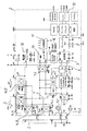
図1のブロック図は、車載(オンボード)ネットワーク(回路網)における電流をモニタする目的で使用される本発明による測定回路1の回路構成を具体的に示す。
【0018】
車載(オンボード)ネットワークは、バッテリ(電池)BATT、2個の抵抗R1、R2、スイッチング素子2、および精密な測定抵抗Rshの形でごく概略的に示されており、測定抵抗Rshの両端間の降下電圧は車両用オンボード・ネットワーク中の電流を表わす。
【0019】
測定回路1が2個の信号入力RSHHおよびRSHLを含むのは、これら2個の信号入力を精密な測定抵抗Rshの2個の端子に接続して、この測定抵抗Rshの両端子間の電圧を差動的に(差電圧を)測定することができるようにするためである。
【0020】
さらに測定回路1は、車両用オンボード・ネットワークのスイッチング素子2と抵抗R2の間の接続点に接続されたバッテリ電圧入力VBATを有している。
【0021】
さらに測定回路1は、可変抵抗を具えたセンサ3が接続された信号入力ETSを有している。
【0022】
最後に、測定回路1は、抵抗Rrefを介してアース(接地点)に接続されたもう1つの信号入力ETRを有している。
【0023】
入力VBAT、ETSおよびETRに接続されたセンサ/抵抗は、各入力に接続可能な内蔵(インストール)された電流源18を介して測定回路によって付勢され、上記電流源18はプログラム可能で且つディジタル的に制御される。それによって生じた電圧降下は、次いで同じ入力でセンサ信号として検出される。
【0024】
信号入力RSHL、RSHH、VBAT、ETSおよびETRは、周波数20kHzで動作するチョッパ4.1〜4.5にそれぞれ接続されている。個々のチョッパ4.1〜4.5は、入力保護回路と入力マルチプレクサとを含んでいる。これらのチョッパは、オフセット抑制およびノイズの影響を最適化するために、測定回路1のチップ上の信号入力RSHL、RSHH、VBAT、ETSおよびETRの接点に直接接続されて配設されている。
【0025】
チョッパ4.1は、双極(バイポーラ)接続によって2個の信号入力RSHHおよびRSHLに(直接)接続され、双極性配線(バイポーラ・ライン)はオフセット、ドリフトおよびノイズ、さらに外部の干渉磁界(電界)に対する感度(EMV感度)を低減する。
【0026】
チョッパ4.3は、同様に双極性配線によって2個の信号入力VBATおよびETSに(直接)接続され、チョッパ4.2、4.4および4.5は共通のアース線およびスイッチング素子M3を介してアースに接続されている。
【0027】
チョッパ4.1の出力は、利得がプログラム可能な増幅器5に接続されている。
【0028】
他のチョッパ4.2〜4.5の出力は、双極性(バイポーラ)電圧バス11に接続され、該電圧バス11は増幅器12(バッファ)を介してマルチプレクサ6に接続されている。従って、マルチプレクサ6は増幅器5によって増幅されたチョッパ4.1の信号、または電圧バス11に供給されたチョッパ4.2〜4.5の中の1つのチョッパ信号のいずれかを変調器7に伝送することができる。
【0029】
さらに、電圧バス11は、他のマルチプレクサ13を介して増幅器5の入力に接続されている。これによって増幅器5は、その入力側でチョッパ4.1の信号、または電圧バス11に印加された信号のいずれかを受信することができる。
【0030】
ディジタル部は、増幅器のこれらの2個の入力チャネル間で切換えを行うことができる制御モードを含み、それによって唯1個のA/D変換器を用いて擬似(準)2チャネル測定が可能になる。この場合、電流測定(チョッパ4.1)と電圧バス上の測定(チョッパ4.2〜4.6)の間で自動切換えが行われる。測定パラメータ(増幅、測定速度、チャネル、等)の選択および調整は、測定開始前に、ディジタル領域での内部レジスタの書込みによって行われる。
【0031】
さらに、測定回路1は、温度センサ14を含み、その出力は別のチョッパ4.6に接続されている。この別のチョッパ4.6の出力は電圧バス11に接続されている。
【0032】
増幅器5の出力は、マルチプレクサ6を介して、変調器7とデシメータ(間引器)8とを含むシグマ-デルタ変換器に接続されており、該シグマ-デルタ変換器の出力はディジタル信号をディジタル回路9に導く。復調すなわちデチョッピング(逆チョッピング“dechopping”)はディジタル部で行われ、従来のチョッパ増幅器の場合のように回路のアナログ部では行われない。
【0033】
測定サイクル(周期)中、マルチプレクサの各極性で4回(または8回)の測定が実行され、そのうちアナログ部の避けられない過渡現象のために最後の値のみがオフセット補償された測定値のディジタル計算に利用される。更新され且つ充分にオフセット補償された測定値は、それぞれ異なる(他の)符号をもった最後の所定測定値がディジタル計算に利用できるので、連続する測定期間の通常の変換時間後に有効に使用される。
【0034】
ディジタル回路9は、さらに測定信号を出力するディジタル・インタフェース10に接続されている。
【0035】
さらに、測定回路1は、2個の信号入力RSHHおよびRSHLに接続された接続ラインの遮断もしくは故障を検出することができる。そのために測定回路1は、2個の信号入力RSHHおよびRSHLに接続され、かつ測定電流を供給すことができる2個の切換え可能な電流源15.1および15.2を有している。2個の信号入力RSHHおよびRSHLにおける差電圧を測定することによって、接続ラインが遮断もしくは故障しているか否かを検出することができる。
【0036】
同様の方法で、内部電源17を接続することによって、入力VBAT、ETRおよびETSにおける接続ラインの切断(故障)を検査することができる。
【0037】
最後に、測定回路1は、入力信号のアナログ・オフセットを供給電圧の約半分にし、それによって最大で+/−0.7Vまでの正および負の値をもった入力電圧を等しい精度で測定することができる。そのために測定回路1は、タイミング回路16および17を有し、その出力は変調器7に接続され、その入力は基準入力REFおよびアナログ・アース入力AGNDに接続されている。
【0038】
この回路は、また、正確な基準電圧を有し、その絶対値および温度係数はディジタル・インタフェースによってトリミング(除去)できる。
【0039】
この測定回路は、さらに、消費電流(電力)を低減するために全機能群を遮断する、いわゆる「スリープモード“Sleep-Modus、sleep mode”」を含んでいる。このときの供給電流は100μAより小さくなる。
【0040】
特殊な1つの特徴として、前記モードで付勢(作動)可能の「アクティブ・ウェイクアップ・モード“Aktive Wake-Up-Modus、active wake-up mode”」がある。この場合、ディジタル領域内に配置された内部オシレータ/タイマによって測定回路は毎秒約1回付勢され、プレプログラミングされた測定が実行される。また、この測定期間中にプレプログラミングされた限界値を超過したことが検出(決定)されると、出力回路は再び付勢され、外部の高次(上位)電子モジュールをウェイクアップする(動作可能状態にする)ことが可能になる。欠陥(エラー)が検出されないときは、回路が次の付勢まで「スリープモード」に戻る。
【0041】
上述の測定回路は、特開2000−235050号公報、欧州特許公開第EP1030185(A1)号明細書および米国特許第6489693(B1)号に記載されているように、個々の負荷(電力消費体)をモニタし、および/またはバッテリ(電池)の電流を、そのバッテリの寿命を延長するように制御するために、車両のバッテリから接続された負荷(電力消費体)へ流れる全電流を測定し、および/または車両のバッテリの充電電流を測定するために有効に使用することができる。また前記米国特許第6489693(B1)号明細書の開示内容を参照により組込む。それによれば、測定回路1を合金からなる測定抵抗の表面上に配設することができる。
【0042】
本発明は、好ましい実施形態を表わす上述のASICに制限されるものではない。むしろ本発明の思想を採用し、特許請求の範囲によってのみ制限される保護範囲に属する多数の変形、修正(変更)が想到可能であることは言うまでもない。
【図面の簡単な説明】
【図1】図1は本発明の測定回路の一実施形態をブロック図の形式で示した図である。
【符号の説明】
1 測定回路
4.1〜4.6 チョッパ
5 増幅器
6 マルチプレクサ
7 変調器
9 ディジタル回路
10 インタフェース
11 電圧バス
12 増幅器
13 マルチプレクサ
15.1、15.2 電流源
16 タイミング回路
17 内部電源
RSHH 信号入力
RSHL 信号入力
VBAT 信号入力
ETS 信号入力
ETR 信号入力
Rsh 測定抵抗
R1、R2 抵抗[0001]
BACKGROUND OF THE INVENTION
The present invention relates to a measurement circuit, in particular an ASIC (application specific integration) for measuring current, voltage and temperature according to the premise part (superordinate concept) of claim 1 (for example in an in-vehicle (onboard, built-in) network). Circuit).
[0002]
[Prior art]
Japanese Laid-Open Patent Publication No. 2000-23503 (Patent Application No. 2000-37016), European Patent Application EP1030185 (A2), and US Pat. No. 6,489,893 (B1) disclose an ASIC (Application-Specific Integrated Circuit). ”) And monitors the current in the vehicle (on-board) network to detect faulty, faulty or faulty loads (power consumers) or battery (battery) overload A measuring circuit for (monitoring) is disclosed.
[0003]
For measuring analog signals, so-called choppers or chopper amplifiers are used, among others. The chopper amplifier can reduce input offset (input offset voltage) and its temperature drift (variation), and low frequency interference. This type of chopper amplifier includes an input-side chopper (Zerhacker, Chopper), a post-stage amplifier, and an output-side demodulator that performs chopping (chopper processing) and phase-synchronizes rectified measurement signals.
[0004]
[Problems to be solved by the invention]
However, these known chopper amplifier circuits are unsatisfactory (insufficient) to cope with noise conditions, have incomplete suppression of input offset voltage, and can only be used in the form of separate amplifier circuits. There is a fact that there is.
[0005]
The present invention is therefore connected in series with a common output circuit in the digital environment of an analog-to-digital converter in such a way that the digital part (section) does not have any adverse effect on the amplifier and the demodulation is done digitally. It is constructed on the basis of integrating physically optimized chopper amplifier circuits for a plurality of input channels.
[0006]
This object is achieved by the features of
[Means for Solving the Problems]
[0007]
The present invention includes a general technical idea in which one chopper is provided for each input signal in a chopper amplifier circuit having a plurality of signal inputs. In one embodiment of the measurement circuit implemented in the form of an integrated circuit, each chopper is preferably connected to the input contact of the chip with its respective input protection circuit in order to optimize its chopper action. Installed directly (attached).
[0008]
In a preferred embodiment of the invention, the measuring circuit comprises a temperature sensor in order to compensate for the temperature dependence of the measurement. In this case, the individual choppers are preferably arranged downstream (downstream) of the temperature sensor.
[0009]
Preferably, the chopper itself simultaneously configures each multiplexer for delivering the measurement signal onto the voltage bus. The signal is supplied from this voltage bus to an amplifier or AD converter by another multiplexer circuit.
[0010]
In a preferred embodiment of the present invention, an analog / digital converter is provided between the amplifier and the demodulator for converting the amplified chopper signal into a digital signal, so that subsequent demodulation is performed digitally. Can do.
[0011]
An analog / digital converter of this type preferably has a filter with a programmable sequence number (Ordnungszahl, order number, ordinal, instruction number, order) and oversampling the analog / digital converter (oversampling). The sampling ratio and oversampling clock frequency are preferably adjustable in addition to the sequence number.
[0012]
In one embodiment of the present invention, the line layout (arrangement, routing) for all input signals is done in a bipolar manner to allow differential measurements, thereby offset, drift, noise and External interference is reduced. Therefore, all wiring line layouts between the signal input and the chopper, between the chopper and the amplifier, and between the amplifier and the A / D converter are preferably formed in a bipolar manner, and therefore preferably in close proximity of the conductors. Trace is used.
[0013]
Furthermore, in a preferred embodiment of the present invention, a sigma-delta converter for converting the chopped (choppered) and amplified measurement signal into a digital signal is arranged after the amplifier.
[0014]
More preferably, a measurement line connected to the input side and a sensor failure detector for detecting the interruption of the sensor are provided. For this purpose, a controllable power supply is preferably provided that can be connected to at least one of the signal inputs. By measuring the voltage of each signal input, it is possible to detect whether or not the measurement line and sensor connected to the input side are cut off.
[0015]
The present invention is particularly suitable for measuring very small bipolar signals, and unlike the known converters to be compared, additional preamplifiers and multiplexers that are costly to process similar small voltages There is an advantage that it is not necessary.
[0016]
Other preferred configurations of the invention developed are contained in the dependent claims and will be described in more detail below with reference to preferred embodiments of the invention shown in the drawings. In the drawing, a preferred embodiment of a measuring circuit according to the invention is shown in block diagram form.
[0017]
DETAILED DESCRIPTION OF THE INVENTION
The block diagram of FIG. 1 specifically shows the circuit configuration of the
[0018]
The on-board network is shown very schematically in the form of a battery (battery) BATT, two resistors R1, R2, a
[0019]
The
[0020]
Furthermore, the
[0021]
Furthermore, the
[0022]
Finally, the measuring
[0023]
Sensors / resistors connected to the inputs VBAT, ETS and ETR are energized by the measurement circuit via a built-in
[0024]
The signal inputs RSHL, RSHH, VBAT, ETS and ETR are connected to choppers 4.1 to 4.5 operating at a frequency of 20 kHz, respectively. Each chopper 4.1-4.5 includes an input protection circuit and an input multiplexer. These choppers are arranged directly connected to the contacts of the signal inputs RSHL, RSHH, VBAT, ETS and ETR on the chip of the
[0025]
The chopper 4.1 is connected (directly) to the two signal inputs RSHH and RSHL by bipolar (bipolar) connections, and the bipolar wiring (bipolar line) is offset, drift and noise, as well as external interference magnetic fields (electric fields). The sensitivity to EMV (EMV sensitivity) is reduced.
[0026]
The chopper 4.3 is likewise connected (directly) to the two signal inputs VBAT and ETS by means of bipolar wiring, and the choppers 4.2, 4.4 and 4.5 are connected via a common ground line and the switching element M3. Connected to ground.
[0027]
The output of the chopper 4.1 is connected to an
[0028]
The outputs of the other choppers 4.2 to 4.5 are connected to a bipolar (bipolar)
[0029]
Furthermore, the
[0030]
The digital section includes a control mode that can be switched between these two input channels of the amplifier, thereby enabling pseudo (quasi) two-channel measurements using only one A / D converter. Become. In this case, automatic switching is performed between the current measurement (chopper 4.1) and the measurement on the voltage bus (choppers 4.2 to 4.6). Measurement parameters (amplification, measurement speed, channel, etc.) are selected and adjusted by writing internal registers in the digital domain before starting the measurement.
[0031]
Furthermore, the measuring
[0032]
The output of the
[0033]
During the measurement cycle (period), four (or eight) measurements are performed for each polarity of the multiplexer, of which only the last value is offset-compensated due to inevitable transients in the analog part. Used for calculation. Updated and fully offset compensated measurements are effectively used after the normal conversion time of successive measurement periods, since the last predetermined measurement with a different (other) sign is available for digital computation. The
[0034]
The
[0035]
Furthermore, the measuring
[0036]
By connecting the
[0037]
Finally, the measuring
[0038]
This circuit also has an accurate reference voltage whose absolute value and temperature coefficient can be trimmed (removed) by a digital interface.
[0039]
The measurement circuit further includes a so-called “sleep mode” that cuts off all functional groups in order to reduce current consumption (power). The supply current at this time is smaller than 100 μA.
[0040]
As a special feature, there is an “active wake-up mode” that can be activated (operated) in the mode. In this case, the measurement circuit is energized about once per second by an internal oscillator / timer located in the digital domain, and a preprogrammed measurement is performed. Also, if it is detected (determined) that the preprogrammed limit value has been exceeded during this measurement period, the output circuit is re-energized and wakes up the external higher order (upper) electronic module (operational) State). If no defects are detected, the circuit returns to “sleep mode” until the next activation.
[0041]
The above-described measuring circuit includes individual loads (power consumers) as described in Japanese Patent Application Laid-Open No. 2000-235050, European Patent Publication No. EP1030185 (A1) and US Pat. No. 6,489,893 (B1). To monitor and / or control the battery (battery) current to extend the life of the battery, measure the total current flowing from the vehicle battery to the connected load (power consumer), And / or can be effectively used to measure the charging current of a vehicle battery. The disclosure of the above-mentioned US Pat. No. 6,489,893 (B1) is incorporated by reference. According to this, the measuring
[0042]
The present invention is not limited to the ASIC described above that represents the preferred embodiment. Rather, it goes without saying that many variations and modifications (changes) belonging to the scope of protection limited by the scope of claims can be conceived by employing the idea of the present invention.
[Brief description of the drawings]
FIG. 1 is a block diagram of an embodiment of a measurement circuit according to the present invention.
[Explanation of symbols]
DESCRIPTION OF
Claims (18)
(b)それぞれが上記の各信号入力(RSHH−RSHL、VBAT−RSHL、ETS−RSHL、ETR−RSHL、VBAT−ETS)に接続されたチョッパを含む複数の後段チョッパ(4.1〜4.6)と、
(c)上記個々の信号入力(RSHH−RSHL、VBAT−RSHL、ETS−RSHL、ETR−RSHL、VBAT−ETS)と上記チョッパ(4.1〜4.5)との間を接続する双極性配線ラインと、
(d)上記チョッパ(4.1〜4.6)の出力側が接続された増幅器(5)と、
(e)出力信号を供給する信号出力(10)と、
を含み、
特徴として、さらに
(f)ディジタル復調器としての機能を有するディジタル信号処理ユニット(9)と、
(g)アナログ−ディジタル変換器(7、8)と、
を含み、
(h)上記アナログ−ディジタル変換器(7、8)は上記増幅器(5)と上記ディジタル信号処理ユニット(9)の間に配置されており、
(i)上記ディジタル信号処理ユニット(9)は上記アナログ−ディジタル変換器(7、8)と上記信号出力(10)の間に配置されており、
(j)上記アナログ−ディジタル変換器(7、8)は増幅されたチョッパの信号をディジタル信号に変換するのに適合しており、
(k)上記ディジタル信号処理ユニット(9)はデチョッピングするのに適合している、
電流および電圧を測定する測定回路。(A) a plurality of signal inputs (RSHH-RSHL, VBAT-RSHL, ETS-RSHL, ETR-RSHL, VBAT-ETS) for receiving respective analog input signals;
(B) A plurality of subsequent choppers (4.1 to 4.6) each including a chopper connected to each of the signal inputs (RSHH-RSHL, VBAT-RSHL, ETS-RSHL, ETR-RSHL, VBAT-ETS). )When,
(C) Bipolar wiring that connects between the individual signal inputs (RSHH-RSHL, VBAT-RSHL, ETS-RSHL, ETR-RSHL, VBAT-ETS) and the chopper (4.1-4.5) Line,
(D) an amplifier (5) to which the output side of the chopper (4.1 to 4.6) is connected;
(E) a signal output (10) for supplying an output signal;
Including
(F) a digital signal processing unit (9) having a function as a digital demodulator;
(G) an analog-digital converter (7, 8);
Including
(H) The analog-digital converter (7, 8) is disposed between the amplifier (5) and the digital signal processing unit (9),
(I) The digital signal processing unit (9) is disposed between the analog-digital converter (7, 8) and the signal output (10),
(J) The analog-to-digital converter (7, 8) is adapted to convert the amplified chopper signal into a digital signal;
(K) the digital signal processing unit (9) is adapted to dechop;
A measurement circuit that measures current and voltage.
Applications Claiming Priority (4)
| Application Number | Priority Date | Filing Date | Title |
|---|---|---|---|
| DE10221426.3 | 2002-05-14 | ||
| DE10221426 | 2002-05-14 | ||
| DE10237126.1 | 2002-08-13 | ||
| DE10237126.1A DE10237126B4 (en) | 2002-05-14 | 2002-08-13 | measuring circuit |
Publications (3)
| Publication Number | Publication Date |
|---|---|
| JP2003329713A JP2003329713A (en) | 2003-11-19 |
| JP2003329713A5 JP2003329713A5 (en) | 2006-06-22 |
| JP4291616B2 true JP4291616B2 (en) | 2009-07-08 |
Family
ID=29271589
Family Applications (1)
| Application Number | Title | Priority Date | Filing Date |
|---|---|---|---|
| JP2003133930A Expired - Lifetime JP4291616B2 (en) | 2002-05-14 | 2003-05-13 | Measurement circuit |
Country Status (3)
| Country | Link |
|---|---|
| US (1) | US6946845B2 (en) |
| EP (1) | EP1363131B1 (en) |
| JP (1) | JP4291616B2 (en) |
Families Citing this family (27)
| Publication number | Priority date | Publication date | Assignee | Title |
|---|---|---|---|---|
| DE102004040575A1 (en) * | 2004-08-21 | 2006-02-23 | Abb Patent Gmbh | Device for measuring electrical current, voltage and temperature on an electrical conductor made of rigid material |
| US7697909B2 (en) * | 2004-09-01 | 2010-04-13 | National Semiconductor Corporation | Extended range RMS-DC converter |
| JP2006317402A (en) * | 2005-05-16 | 2006-11-24 | Fuji Electric Systems Co Ltd | Current sensor and watt-hour arithmetic unit |
| JP2009258009A (en) * | 2008-04-18 | 2009-11-05 | Panasonic Corp | Physical quantity detecting circuit and physical quantity sensor device having the same |
| DE102009031408A1 (en) | 2009-07-01 | 2011-01-05 | Isabellenhütte Heusler Gmbh & Co. Kg | Electronic component and corresponding manufacturing method |
| DE102010009835A1 (en) | 2010-03-02 | 2011-09-08 | Isabellenhütte Heusler Gmbh & Co. Kg | Electronic component, in particular current sensor |
| DE202010010152U1 (en) | 2010-07-13 | 2010-10-14 | Isabellenhütte Heusler Gmbh & Co. Kg | Current measurement module |
| DE102011111081B4 (en) | 2011-08-18 | 2021-08-05 | Isabellenhütte Heusler Gmbh & Co. Kg | Battery sensor |
| DE102012001883B3 (en) | 2012-02-01 | 2013-04-25 | Isabellenhütte Heusler Gmbh & Co. Kg | Soldering method and corresponding soldering device |
| CN102590602A (en) * | 2012-02-13 | 2012-07-18 | 西安爱邦电气有限公司 | Signal processing method by adopting public processing circuit during collection of alternating-current voltage and current |
| DE102012219945A1 (en) * | 2012-10-31 | 2014-04-30 | Robert Bosch Gmbh | Method for measuring electric current, involves detecting measuring voltage between measurement points by voltage measuring unit, and detecting current flowing along measurement path based on voltage detected with open switch |
| ES2534391T3 (en) | 2012-11-30 | 2015-04-22 | Isabellenhütte Heusler Gmbh & Co.Kg | Battery sensor |
| US9329042B1 (en) * | 2013-01-08 | 2016-05-03 | Maxim Integrated Products, Inc. | Innovative angular sensor read-out multi-axes digital front-end chain |
| CN205691648U (en) | 2013-02-25 | 2016-11-16 | 伊莎贝尔努特·霍伊斯勒两合公司 | There is multiple sensor and there is the measurement system of central analysis evaluation unit |
| DE102013009726A1 (en) | 2013-06-10 | 2014-12-11 | Isabellenhütte Heusler Gmbh & Co. Kg | Stamped part for producing an electrical resistance, current sensor and corresponding manufacturing method |
| CN104656022A (en) * | 2013-11-20 | 2015-05-27 | 上海航天有线电厂 | Measuring circuit for voltage of single batteries of series lithium battery pack based on optocoupler relays |
| DE102014011593B4 (en) | 2014-08-01 | 2016-05-04 | Isabellenhütte Heusler Gmbh & Co. Kg | Resistance, in particular low-impedance current measuring resistor |
| KR102345505B1 (en) * | 2015-06-08 | 2021-12-29 | 삼성에스디아이 주식회사 | Current detecting circuit |
| DE102016202498A1 (en) * | 2016-02-18 | 2017-08-24 | Continental Automotive Gmbh | Measuring resistance calibration device, method for calibrating a measuring resistor and battery sensor |
| DE102016010012B4 (en) | 2016-08-17 | 2018-06-21 | Isabellenhütte Heusler Gmbh & Co. Kg | Measuring arrangement for measuring an electric current in the high current range |
| DE102016014130B3 (en) * | 2016-11-25 | 2017-11-23 | Isabellenhütte Heusler Gmbh & Co. Kg | Current measuring device |
| US11555831B2 (en) | 2020-08-20 | 2023-01-17 | Vishay Dale Electronics, Llc | Resistors, current sense resistors, battery shunts, shunt resistors, and methods of making |
| CN112543001B (en) * | 2020-12-04 | 2023-09-19 | 江苏科技大学 | Front chopper amplifier capable of separating local field potential and action potential |
| CN113985104B (en) * | 2021-10-27 | 2023-09-01 | 四川创安微电子有限公司 | Circuit and method for detecting voltage and current signals in chip |
| DE102022005032A1 (en) | 2022-04-22 | 2023-11-02 | Isabellenhütte Heusler Gmbh & Co. Kg | Current measuring device and associated manufacturing process |
| DE102022109708B4 (en) | 2022-04-22 | 2023-12-14 | Isabellenhütte Heusler Gmbh & Co. Kg | Current measuring device and associated manufacturing process |
| DE102022109709B4 (en) | 2022-04-22 | 2023-12-14 | Isabellenhütte Heusler Gmbh & Co. Kg | Current measuring device and associated manufacturing process |
Family Cites Families (8)
| Publication number | Priority date | Publication date | Assignee | Title |
|---|---|---|---|---|
| US3344406A (en) | 1964-11-09 | 1967-09-26 | Ibm | Sampled data reduction and storage system |
| DE2451281C3 (en) | 1974-10-29 | 1979-03-01 | Eckardt Ag, 7000 Stuttgart | Measuring amplifier |
| US3992617A (en) | 1975-10-01 | 1976-11-16 | International Telephone And Telegraph Corporation | Chopping correlator for a MSK data signal |
| US4694384A (en) | 1986-12-04 | 1987-09-15 | General Electric Company | HVIC power supply controller with primary-side edge detector |
| US5339018A (en) * | 1989-06-30 | 1994-08-16 | Analog Devices, Inc. | Integrated circuit monitor for storage battery voltage and temperature |
| US5287107A (en) * | 1992-06-05 | 1994-02-15 | Hewlett-Packard Company | Optical isolation amplifier with sigma-delta modulation |
| US5869951A (en) * | 1994-10-26 | 1999-02-09 | Fuji Jukogyo Kabushiki Kaisha | Battery management system for electric vehicle |
| US6324042B1 (en) * | 1999-03-12 | 2001-11-27 | Lynntech, Inc. | Electronic load for the testing of electrochemical energy conversion devices |
-
2003
- 2003-05-07 US US10/431,292 patent/US6946845B2/en not_active Expired - Lifetime
- 2003-05-09 EP EP03010486A patent/EP1363131B1/en not_active Expired - Lifetime
- 2003-05-13 JP JP2003133930A patent/JP4291616B2/en not_active Expired - Lifetime
Also Published As
| Publication number | Publication date |
|---|---|
| US6946845B2 (en) | 2005-09-20 |
| EP1363131B1 (en) | 2008-08-20 |
| JP2003329713A (en) | 2003-11-19 |
| EP1363131A1 (en) | 2003-11-19 |
| US20030222511A1 (en) | 2003-12-04 |
Similar Documents
| Publication | Publication Date | Title |
|---|---|---|
| JP4291616B2 (en) | Measurement circuit | |
| EP1632779B1 (en) | Hall sensor module and integrated circuit for use with an external Hall sensor | |
| JP4719972B2 (en) | Charge / discharge current measuring device | |
| CN102243291A (en) | Method for measuring accumulator power in motor car | |
| US20240044954A1 (en) | Current sensing circuitry | |
| JP2003282158A (en) | Battery voltage measuring circuit | |
| JP4451415B2 (en) | Current / voltage conversion circuit | |
| CN111123106B (en) | Sensor and method for checking a sensor | |
| JP4479086B2 (en) | Voltage detection device for battery pack | |
| JP6718284B2 (en) | Signal processing circuit, coulomb counter circuit, electronic device | |
| JP4511771B2 (en) | Voltage applied current measuring device and semiconductor test device | |
| JP2002050406A (en) | Current detection device and battery device equipped with the same | |
| JP3815607B2 (en) | Temperature transmitter using analog-digital converter | |
| JPH0663801B2 (en) | Flow rate measurement circuit | |
| WO2002037298A2 (en) | Configurable mixed analog and digital mode controller system | |
| JP2539425Y2 (en) | Temperature measurement input circuit | |
| JP3978672B2 (en) | Voltage applied current measuring instrument | |
| JPH07124554A (en) | Method and device for detecting water flow for water purifier | |
| DE10237126B4 (en) | measuring circuit | |
| JPH11337430A (en) | Bridge-type sensor | |
| Johnston | A Collection of Bridge Transducer Digitizer Circuits | |
| JPH088431Y2 (en) | Resistance measurement device | |
| CN117419823A (en) | Temperature acquisition circuit and device | |
| JP2004080692A (en) | Electronic circuit | |
| WO1999060340A2 (en) | Measurement circuit employing dual floating power supplies |
Legal Events
| Date | Code | Title | Description |
|---|---|---|---|
| A521 | Request for written amendment filed |
Free format text: JAPANESE INTERMEDIATE CODE: A523 Effective date: 20060428 |
|
| A621 | Written request for application examination |
Free format text: JAPANESE INTERMEDIATE CODE: A621 Effective date: 20060428 |
|
| A977 | Report on retrieval |
Free format text: JAPANESE INTERMEDIATE CODE: A971007 Effective date: 20080731 |
|
| A131 | Notification of reasons for refusal |
Free format text: JAPANESE INTERMEDIATE CODE: A131 Effective date: 20080805 |
|
| A521 | Request for written amendment filed |
Free format text: JAPANESE INTERMEDIATE CODE: A523 Effective date: 20081105 |
|
| RD13 | Notification of appointment of power of sub attorney |
Free format text: JAPANESE INTERMEDIATE CODE: A7433 Effective date: 20081208 |
|
| A131 | Notification of reasons for refusal |
Free format text: JAPANESE INTERMEDIATE CODE: A131 Effective date: 20081209 |
|
| A521 | Request for written amendment filed |
Free format text: JAPANESE INTERMEDIATE CODE: A821 Effective date: 20081208 |
|
| A521 | Request for written amendment filed |
Free format text: JAPANESE INTERMEDIATE CODE: A523 Effective date: 20090306 |
|
| TRDD | Decision of grant or rejection written | ||
| A01 | Written decision to grant a patent or to grant a registration (utility model) |
Free format text: JAPANESE INTERMEDIATE CODE: A01 Effective date: 20090325 |
|
| A01 | Written decision to grant a patent or to grant a registration (utility model) |
Free format text: JAPANESE INTERMEDIATE CODE: A01 |
|
| A61 | First payment of annual fees (during grant procedure) |
Free format text: JAPANESE INTERMEDIATE CODE: A61 Effective date: 20090403 |
|
| R150 | Certificate of patent or registration of utility model |
Ref document number: 4291616 Country of ref document: JP Free format text: JAPANESE INTERMEDIATE CODE: R150 Free format text: JAPANESE INTERMEDIATE CODE: R150 |
|
| FPAY | Renewal fee payment (event date is renewal date of database) |
Free format text: PAYMENT UNTIL: 20120410 Year of fee payment: 3 |
|
| FPAY | Renewal fee payment (event date is renewal date of database) |
Free format text: PAYMENT UNTIL: 20130410 Year of fee payment: 4 |
|
| R250 | Receipt of annual fees |
Free format text: JAPANESE INTERMEDIATE CODE: R250 |
|
| FPAY | Renewal fee payment (event date is renewal date of database) |
Free format text: PAYMENT UNTIL: 20140410 Year of fee payment: 5 |
|
| R250 | Receipt of annual fees |
Free format text: JAPANESE INTERMEDIATE CODE: R250 |
|
| S111 | Request for change of ownership or part of ownership |
Free format text: JAPANESE INTERMEDIATE CODE: R313114 |
|
| R350 | Written notification of registration of transfer |
Free format text: JAPANESE INTERMEDIATE CODE: R350 |
|
| R250 | Receipt of annual fees |
Free format text: JAPANESE INTERMEDIATE CODE: R250 |
|
| R250 | Receipt of annual fees |
Free format text: JAPANESE INTERMEDIATE CODE: R250 |
|
| R250 | Receipt of annual fees |
Free format text: JAPANESE INTERMEDIATE CODE: R250 |
|
| R250 | Receipt of annual fees |
Free format text: JAPANESE INTERMEDIATE CODE: R250 |
|
| R250 | Receipt of annual fees |
Free format text: JAPANESE INTERMEDIATE CODE: R250 |
|
| R250 | Receipt of annual fees |
Free format text: JAPANESE INTERMEDIATE CODE: R250 |
|
| R250 | Receipt of annual fees |
Free format text: JAPANESE INTERMEDIATE CODE: R250 |
|
| R250 | Receipt of annual fees |
Free format text: JAPANESE INTERMEDIATE CODE: R250 |
|
| R250 | Receipt of annual fees |
Free format text: JAPANESE INTERMEDIATE CODE: R250 |
|
| R250 | Receipt of annual fees |
Free format text: JAPANESE INTERMEDIATE CODE: R250 |
|
| EXPY | Cancellation because of completion of term |