JP4281237B2 - Self-scanning light emitting device array chip - Google Patents
Self-scanning light emitting device array chip Download PDFInfo
- Publication number
- JP4281237B2 JP4281237B2 JP2000295553A JP2000295553A JP4281237B2 JP 4281237 B2 JP4281237 B2 JP 4281237B2 JP 2000295553 A JP2000295553 A JP 2000295553A JP 2000295553 A JP2000295553 A JP 2000295553A JP 4281237 B2 JP4281237 B2 JP 4281237B2
- Authority
- JP
- Japan
- Prior art keywords
- transfer
- transfer element
- clock pulse
- threshold voltage
- light emitting
- Prior art date
- Legal status (The legal status is an assumption and is not a legal conclusion. Google has not performed a legal analysis and makes no representation as to the accuracy of the status listed.)
- Expired - Fee Related
Links
- 230000003287 optical effect Effects 0.000 claims description 19
- 238000011144 upstream manufacturing Methods 0.000 claims 16
- 238000010586 diagram Methods 0.000 description 13
- 239000004065 semiconductor Substances 0.000 description 12
- 239000000758 substrate Substances 0.000 description 4
- 238000009792 diffusion process Methods 0.000 description 3
- 239000010408 film Substances 0.000 description 3
- 230000000694 effects Effects 0.000 description 2
- 239000002184 metal Substances 0.000 description 2
- 230000001681 protective effect Effects 0.000 description 2
- 235000012431 wafers Nutrition 0.000 description 2
- 229910021417 amorphous silicon Inorganic materials 0.000 description 1
- 238000003491 array Methods 0.000 description 1
- 230000005540 biological transmission Effects 0.000 description 1
- 230000003111 delayed effect Effects 0.000 description 1
- 239000012535 impurity Substances 0.000 description 1
- 239000000463 material Substances 0.000 description 1
- 230000002441 reversible effect Effects 0.000 description 1
- 239000010409 thin film Substances 0.000 description 1
Images


Landscapes
- Printers Or Recording Devices Using Electromagnetic And Radiation Means (AREA)
- Led Devices (AREA)
Description
【0001】
【発明の属する技術分野】
本発明は、自己走査型発光素子アレイチップ、特に、発光用クロックラインを2分割することにより、1チップ上で2つの発光点を同時に点灯できるようにした自己走査型発光素子アレイチップに関する。
【0002】
【従来の技術】
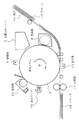
光プリンタの書込みヘッド(光書込みヘッド)は、感光ドラムに光を露光させるための光源であり、発光素子アレイを有している。光書込みヘッドを備える光プリンタの原理図を図1に示す。円筒形の感光ドラム5の表面に、アモルファスSi等の光導電性を持つ材料(感光体)が作られている。このドラムはプリントの速度で回転している。回転しているドラムの感光体表面を、帯電器6で一様に帯電させる。そして、光書込みヘッド7で、印字するドットイメージの光を感光体上に照射し、光の当たったところの帯電を中和し、潜像を形成する。続いて、現像器8で感光体上の帯電状態にしたがって、トナーを感光体上につける。そして、転写器10でカセット12中から送られてきた用紙14上に、トナーを転写する。用紙は、定着器16にて熱等を加えられ定着され、スタッカ18に送られる。一方、転写の終了したドラムは、消去ランプ20で帯電が全面にわたって中和され、清掃器22で残ったトナーが除去される。
【0003】
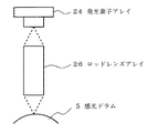
光書込みヘッド7の構造を図2に示す。光書込みヘッドは発光素子アレイ24と正立等倍光学系、例えばロッドレンズアレイ26で構成され、レンズの焦点が感光ドラム5上に結ぶようになっている。
【0004】
本発明者らは、自己走査型の発光素子アレイの構成要素として、pnpn構造を持つ3端子発光サイリスタに注目し、既に特許出願(特開平1−238962号公報、特開平2−14584号公報、特開平2−92650号公報、特開平2−92651号公報)し、光プリンタ用光源として実装上簡便となること、発光素子ピッチを細かくできること、コンパクトな自己走査型発光素子アレイを作製できること等を示した。
【0005】
さらに本発明者らは、転送素子アレイをシフト部として、発光部である発光素子アレイと分離した構造の自己走査型発光素子アレイを提案している(特開平2−263668号公報)。
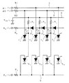
【0006】
図3に、シフト部と発光部とを分離した構造の自己走査型発光素子アレイチップの等価回路図を示す。シフト部は、転送素子T1 ,T2 ,T3 ,…を有し、発光部は、書込み用発光素子L1 ,L2 ,L3 ,…を有している。これら転送素子および発光素子は、3端子発光サイリスタにより構成される。シフト部の構成は、転送素子のゲートを互いに電気的に接続するのにダイオードD1 ,D2 ,D3 ,…を用いている。VGKは電源(通常5V)であり、負荷抵抗RL を経て各転送素子のゲート電極G1 ,G2 ,G3 ,…に接続されている。また、転送素子のゲート電極G1 ,G2 ,G3 ,…は、書込み用発光素子のゲート電極にも接続される。転送素子T1 のゲート電極にはスタートパルスφS が加えられ、転送素子のアノード電極には、交互に転送用クロックパルスφ1,φ2が加えられ、書込み用発光素子のアノード電極には、書込み信号φI が加えられている。
【0007】
なお図中、1はφ1ライン、2はφ2ライン、3はφI ライン、4は電源ラインを示し、R1,R2,RI は、φ1ライン,φ2ライン,φI ラインに挿入された電流制限抵抗を示している。
【0008】
動作を簡単に説明する。まず転送用クロックパルスφ1の電圧が、Hレベルで、転送素子T2 がオン状態であるとする。このとき、ゲート電極G2 の電位はVGKの5Vからほぼ零Vにまで低下する。この電位降下の影響はダイオードD2 によってゲート電極G3 に伝えられ、その電位を約1Vに(ダイオードD2 の順方向立上り電圧(拡散電位に等しい))に設定する。しかし、ダイオードD1 は逆バイアス状態であるためゲート電極G1 への電位の接続は行われず、ゲート電極G1 の電位は5Vのままとなる。発光サイリスタのオン電圧は、ゲート電極電位+pn接合の拡散電位(約1V)で近似されるから、次の転送用クロックパルスφ2のHレベル電圧は約2V(転送素子T3 をオンさせるために必要な電圧)以上でありかつ約4V(転送素子T5 をオンさせるために必要な電圧)以下に設定しておけば転送素子T3 のみがオンし、これ以外の転送素子はオフのままにすることができる。従って2本の転送用クロックパルスでオン状態が転送されることになる。
【0009】
スタートパルスφS は、このような転送動作を開示させるためのパルスであり、スタートパルスφS をLレベル(約0V)にすると同時に転送用クロックパルスφ2をHレベル(約2〜約4V)とし、転送素子T 1 をオンさせる。その後すぐ、スタートパルスφS はHレベルに戻される。
【0010】
いま、転送素子T2 がオン状態にあるとすると、ゲート電極G2 の電位は、ほぼ0Vとなる。したがって、書込み信号φI の電圧が、pn接合の拡散電位(約1V)以上であれば、発光素子L2 を発光状態とすることができる。
【0011】
これに対し、ゲート電極G1 は約5Vであり、ゲート電極G3 は約1Vとなる。したがって、発光素子L1 の書込み電圧は約6V、発光素子L3 の書込み電圧は約2Vとなる。これから、発光素子L2 のみに書込める書込み信号φI の電圧は、1〜2Vの範囲となる。発光素子L2 がオン、すなわち発光状態に入ると、発光強度は書込み信号φI に流す電流量で決められ、任意の強度にて画像書込みが可能となる。また、発光状態を次の発光素子に転送するためには、書込み信号φI ラインの電圧を一度0Vまでおとし、発光している発光素子をいったんオフにしておく必要がある。
【0012】
自己走査型発光素子アレイは、上述のような構成のチップを配列することにより作製される。自己走査型発光素子アレイチップの価格は、通常の集積回路同様、1ウエファから取れる個数によって決まる。このため、チップの幅を細くした方が安価になる。
【0013】
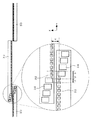
本出願人は、できる限り細幅のチップを実現する構成として、ボンディングパッドを両端(もしくは片端)に寄せたチップを千鳥状に配置することを提案している。ボンディングパッドを片端に寄せたチップを千鳥状に配置した様子を示す模式図を図4に示す。図4には、方向を示すx−y軸を示す。
【0014】
自己走査型発光素子アレイチップ30を、発光点32がx方向にピッチPとなるように配列し、y方向のチップ間の距離dを、y方向解像度rの整数倍にとる。なお図中、34はボンディングパッドを示す。この発光点列の点/滅を、図2で示したように、ロッドレンズアレイを介して、感光ドラム上に投影して潜像を得る。ただし、このままでは、チップ間の発光点列はy方向に距離dだけ離れているので、d/r本分だけ時間的にずれた画像のラインデータを使わなければならない。距離dはある程度大きい方が、書込みヘッドの組立が容易であるが、距離dが大きくなるにつれて、チップ間の光学系伝達効率や焦点位置のズレが大きくなるので、むやみと増やすことはできない。また、距離dを大きくすることは、遅延させるデータ量が増加することとなり、必要メモリを増加させる。
【0015】
【発明が解決しようとする課題】
上述した従来の書込みヘッドで、より高光出力のものを得たい場合、各発光点に流れる電流を増やすか、発光デューティを増加させるために同時に点灯できる発光点の数を増やす必要がある。電流値は、寿命に大きく影響するため、むやみに増やせない場合が多い。そこで、発光デューティを増加させるために同時に点灯できる発光点の数を1チップあたり2個にするために、φI ラインを2本にすると、多層配線を使わない限り、発光素子の外側をφI ラインが通ることになる。このため、発光素子とチップ長辺までの距離が遠くなってしまい、距離dが大きくなってしまう。
【0016】
さらに、同時に発光できる点数を3個以上にするためには、多層配線を使わない限り実現できない。
【0017】
本発明の目的は、チップ間のy方向距離dを大きくすることなく、同時に点灯できる発光点の数を1チップあたり2個にすることのできる自己走査型発光素子アレイチップを提供することにある。
【0018】
本発明の他の目的は、多層配線を用いることなく、同時に点灯できる発光点の数を1チップあたり4個にすることのできる自己走査型発光素子アレイチップを提供することにある。
【0019】
【課題を解決するための手段】
本発明によれば、1つのチップ上に、自己走査型発光素子アレイ回路を2個作り込む。この場合に、φI ラインを各回路毎に独立に設け、それぞれのφI ラインあたり、1個の発光点が点灯できるようにした。
【0020】
各自己走査型発光素子アレイ回路へ2相クロックパルスラインは、各回路毎に独立に設けることもでき、あるいは各回路に共通に設けることもできる。2相クロックパルスラインを共通に設ける場合には、転送素子と各クロックパルスラインとの間に抵抗を設け、この抵抗の値および各クロックパルスラインに挿入された電流制限抵抗の値を、2個の転送素子が同時にオンとなるように選ぶ。
【0021】
また、各自己走査型発光素子アレイ回路において、φI ラインを2本設け、各φI ラインに発光素子を交互に接続すれば、各回路毎に2個の発光点、合計4個の発光点を同時に点灯することが可能となる。
【0022】
このように同時に点灯できる発光素子の数を増やすことにより、発光デューティを大きくできるので、光書込みヘッドの光出力を増大させることが可能となる。
【0023】
【発明の実施の形態】
以下、本発明の実施の形態を、図面に基づいて説明する。
【0024】
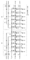
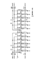
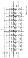
【第1の実施例】
第1の実施例の自己走査型発光素子アレイチップの等価回路を図5に示す。1個のチップに2つの回路を作り込んだものである。図において、左右の回路40,50は、図面を簡単にするためそれぞれ、各6個の発光素子を持った例を示している。
【0025】
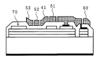
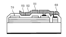
各回路40,50は、図3に示した回路と同じであり、回路40は発光点が左から右へ転送され、回路50は発光が右から左へ転送される構成となっている。各回路を構成する素子は、図3で示した回路と同じである。左側回路40において、φ1L,φ2Lはクロックパルス、φS Lはスタートパルス、φI Lは書込み信号、41はφ1Lライン、42はφ2Lライン、43はφI Lラインを示している。また、右側回路50において、φ1R,φ2Rはクロックパルス、φS Rはスタートパルス、φI Rは書込み信号、51はφ1Rライン、52はφ2Rライン、53はφI Rラインを示している。
【0026】
このように左右の回路ごとに、クロックパルスφ1,φ2、スタートパルスφS 、書込み信号φI をそれぞれ別系統とし、図示のように電源VGKのみは共通とする。共通のVGKラインを60で示す。
【0027】
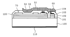
図6は、図5のチップの実際の構成の平面図であり、図7は、図6のX−X′線断面図である。図6および図7において、図5と同じ要素には、同一の参照番号を付して示してある。
【0028】
なお、図6において、44,45,46,47,48および55,56,57,58は、ボンディングパッドを、70は発光部を示している。
【0029】
図7の断面図に示すように、自己走査型発光素子アレイチップは、pnpn構造により作製される。pnpn構造は、n型半導体基板100上に、n型半導体層101,p型半導体層102,n型半導体層103,p型半導体層104が順次積層される。保護膜120上に、φ1ライン51,φ2ライン52,φI ライン53,VGKライン60が設けられている。また、n型半導体基板100の裏面には共通の裏面電極110が設けられている。
【0030】
図5,図6,図7から明らかなように、本実施例の自己走査型発光素子アレイチップは、VGKラインを共通としているが、回路40,50毎に独立しており、2つの自己走査型発光素子アレイを1つのチップに作り込んだ構成となっている。
【0031】
このような構成によれば、φI ラインを左右2本に分割し、それぞれのラインあたり1個の発光点を点灯できる。したがって、発光デューティを増加させることができ、高光出力が得られる。
【0032】
なお、以上の実施例では、左右の回路の発光素子の数を同じにしているが、同じである必要は必ずしもない。
【0033】
さらに、本実施例では、回路40は左から右へ、回路50は右から左へ発光点を転送しているが、必ずしもこの組み合わせである必要はない。しかし実際には、ボンディングパッドをチップの両端に置く構造をとる場合には、スタートパルス端子がチップ両端にあるため、チップの両端から中心に向かって発光点が転送する構成が作りやすい。
【0034】
【第2の実施例】
第1の実施例では、単純に2つの自己走査型発光素子アレイを1つのチップに作り込んだだけであったため、φ1ライン,φ2ラインが左右別々に存在するため、ボンディングパッドの数が増加し、チップ面積を増加させる。
【0035】
そこで、本実施例では、図5の回路において、φ1Lラインとφ1Rラインを同じボンディングパッドに接続し、φ2Lラインとφ2Rラインとを同じボンディングパッドに接続することで第1の実施例よりもボンディングパッドを2個減らす構成とした。
【0036】
図8に、その回路構成を示す。φ1Lライン41とφ1Rライン51を右側のボンディングパッドに、φ2Lライン42とφ2Rライン52とを左側のボンディングパッドに接続する。
【0037】
図9は、図8のチップの実際の構成の平面図であり、図10は、図9のX−X′線断面図である。図9,図10において、図6,図7と同一の要素には、同一の参照番号を付して示してある。なお、49はφ2パッド、59はφ1パッドを示している。
【0038】
第1の実施例に比べて、パッド数を、2個減らすことができ、したがってチップ面積を小さくすることができる。
【0039】
【第3の実施例】
第1および第2の実施例では、スタートパルス端子を備えているが、ダイオードを用いて、スタートパルスをクロックパルスに兼ねさせることによって、スタートパルス端子を省略することができる。
【0040】
図11に、その回路構成を示す。ダイオード62を、左側回路の左端の転送素子のゲートと、φ2Lライン42との間に挿入し、およびダイオード64を、右側回路の左端の転送素子のゲートと、φ2Rライン52との間に挿入する。
【0041】
図12は、図11のチップの実際の構成の平面図であり、図13は、図12のX−X′線断面図である。なお、図12の左側回路において、66,68は、ダイオード62のカソードおよびアノードをそれぞれ示している。
【0042】
本実施例の回路によれば、φS LボンディングパッドおよびφS Rボンディングパッドを省略できるので、チップの面積を小さくすることができる。さらに、本実施例の回路では、左側回路および右側回路において、共に発光点を左から右へ転送しているが、φS ボンディングパッドの無いこの構成では、スタートする転送素子を自由に選ぶことができるので、転送方向については自由な構成が可能となる。
【0043】
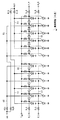
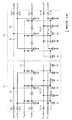
【第4の実施例】
第2の実施例では、φ1,φ2のボンディングパッドは1チップあたり1個にできたが、図8を見ればわかるように、チップ表面を3本分のクロックラインが通るスペースが必要となる。このため、チップ面積が大きくなる問題点がある。そこで、本実施例では、シフト部の転送素子(サイリスタ)のアノードとクロックラインとの間に適当な抵抗RA を設けることにより、2本のクロックラインφ1,φ2で同時に2発光点が点灯できるようにした。
【0044】
図14に、その回路構成を示す。2本のφ1ライン1,φ2ライン2を設け、転送素子(サイリスタ)T1 L,T2 L,T3 L,…、T1 R,T2 R,T3 R,…の各アノードを、抵抗RA を経て、それぞれφ1ライン,φ2ラインに接続する。その他の構成は、図5に同じである。
【0045】
図15は、図14のチップの実際の構成の平面図であり、図16は、図15のX−X′線断面図である。図15において、71はφ1ボンディングパッド、72はφ2ボンディングパッドである。
【0046】
抵抗RA を設けることにより、同時に2点転送ができるメカニズムについて説明する。いま、図14のφS L端子およびφS R端子が基板電位の場合を考える。この場合、サイリスタT1 L,T1 Rのしきい電圧Vthは約VD (pn接合順方向電位)である。クロックパルスφ1がHレベルになり、サイリスタT1 L,T1 Rのいずれかがオンする。オンしたサイリスタのアノードは約VD に固定される。このときのクロックパルスφ1の電圧は、アノード電圧(≒VD )よりも抵抗RA の電圧降下分だけ高い値となる。このため、先にオンできなかったサイリスタも速やかにオンできる。すなわち、サイリスタT1 LとT1 Rとを同時にオンできる。これにより対応する発光素子(サイリスタ)L1 L,L1 Rを同時に点灯できる。
【0047】
このとき、サイリスタT2 LとT2 Rのしきい電圧Vthは、約2VD である。クロックパルスφ2がHレベルとなると、このどちらかがオンできる。このときのサイリスタの電流−電圧(I−V)特性を図17に示す。i=3mAとなるように抵抗RA ,R2およびパルス電圧を選ぶと、φ2ラインの電圧は、オンできなかったサイリスタのしきい電圧(≒2VD )よりも低い値となり、1個しか点灯できない。しかし、電流を増やしていくと、φ2ラインの電圧は上昇していき、ついにはしきい電圧を超え、I−V特性は実線から破線に乗り移り、2つのサイリスタT2 LとT2 Rが同時にオンする。すなわち、RA とR1,R2の値を適当に選ぶことによって、1クロックラインあたり2個以上のサイリスタを同時にオンさせることができる。
【0048】
アノード抵抗RA および電流制限抵抗R1,R2は、2個のサイリスタがオン可能であり、かつ、3個が同時にオンしないように選ぶ(なお、3個目のサイリスタがオンしようとするのは、転送時に起こる)。
【0049】
すなわち、電流jがφ2ラインに流れているとき、2個のサイリスタがオンするには、
Vth<VD +RA ×j
であり、3個以上のサイリスタがオンしないためには、
Vth>VD +RA /2×j
である必要がある。これをjについて解くと、
2(Vth−VD )/RA >j>(Vth−VD )/RA
となる。このjは、クロックパルスのHレベル電圧VH と抵抗R2の値とで決められ、
j=(Vth−VD )+R2
となる。この式の関係およびサイリスタの動作条件を考慮して、RA およびR1,R2の値を決める。図17の負荷曲線の場合、RA =375Ωのとき、411Ω<R1,R2<800Ωとなった。
【0050】
抵抗RA の作り方は、いろいろと考えられるが、ここでは、アノード層エピ膜の不純物濃度を低めに設定し、アノード電極とアノード層の間の接触抵抗が大きめになるように調整し、抵抗RA として用いた。
【0051】
なお、抵抗RA はこのほかの作り方でもよく、例えば、アノード電極と金属配線の間に、抵抗層を設けたり、あるいは、半導体層や金属薄膜などを用いて独立した抵抗を作って接続しても良い。
【0052】
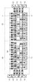
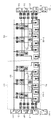
【第5の実施例】
第1〜第4の実施例は、φI ラインを発光素子列の片側に置く構造について示した。しかし、更に光量が必要な場合、発光素子の両側にφI ラインを置き、それぞれを2分割することによって、1チップあたり4発光点を同時に点灯できる。
【0053】
図18に、その回路構成を、図19に、チップの実際の構成を示す。なお、本実施例は、第1の実施例(図5,図6)の構成において、φI Lライン,φI Rラインをそれぞれ2分割した例である。
【0054】
1個の転送素子に対して、2個の発光素子を対応させ、左側回路40では、発光素子を2本のφI Lライン43−1,φI Lライン43−2にそれぞれ交互に接続し、右側回路50では、発光素子を2本のφI Rライン53−1,φI Rライン53−2にそれぞれ交互に接続する。
【0055】
なお、図19において、48−1,48−2は左側回路40のφI L1,φI L2ラインのボンディングパッドを、58−1,58−2は右側回路50のφI R1,φI R2ラインのボンディングパッドを、それぞれ示す。
【0056】
このような構成では、左側回路で2個の発光点と右側回路で2個の発光点とを同時に、すなわち4発光点を同時に点灯させることができる。
【0057】
なお、このような4発光点を同時に点灯させる構成は、第2,第3,第4の実施例についても適用することができる。
【0058】
【発明の効果】
本発明によれば、チップ間のy方向距離を大きくすることなく、同時に点灯できる発光点の数を1チップあたり2個にすることができる。したがって、発光デューティを増大できるので、光書込みヘッドとしての光出力を大きくすることができる。
【0059】
さらに、本発明によれば、多層配線を用いることなく、同時に点灯できる発光点の数を1チップあたり4個にすることのできる自己走査型発光素子アレイチップを提供することが可能となる。
【図面の簡単な説明】
【図1】光書込みヘッドを備える光プリンタの原理を示す図である。
【図2】光書込みヘッドの構造を示す図である。
【図3】シフト部と発光部とを分離した構造の自己走査型発光素子アレイチップの等価回路図である。
【図4】ボンディングパッドを片端に寄せたチップを千鳥状に配置した様子を示す模式図である。
【図5】第1の実施例の自己走査型発光素子アレイチップの等価回路を示す図である。
【図6】図5のチップの実際の構成の平面図である。
【図7】図6のX−X′線断面図である。
【図8】第2の実施例の自己走査型発光素子アレイチップの等価回路を示す図である。
【図9】図8のチップの実際の構成の平面図である。
【図10】図9のX−X′線断面図である。
【図11】第3の実施例の自己走査型発光素子アレイチップの等価回路を示す図である。
【図12】図11のチップの実際の構成の平面図である。
【図13】図12のX−X′線断面図である。
【図14】第4の実施例の自己走査型発光素子アレイチップの等価回路を示す図である。
【図15】図14のチップの実際の構成の平面図である。
【図16】図15のX−X′線断面図である。
【図17】サイリスタのI−V特性を示す図である。
【図18】第5の実施例の自己走査型発光素子アレイチップの等価回路を示す図である。
【図19】図18のチップの実際の構成の平面図である。
【符号の説明】
41 φ1Lライン
42 φ2Lライン
43 φI Lライン
51 φ1Rライン
52 φ2Rライン
53 φI Rライン
60 VGKライン
62,64 ダイオード
44,45,46,47,48,49 ボンディングパッド
55,56,57,58,59 ボンディングパッド
71,72 ボンディングパッド
100 n型半導体基板
101 n型半導体層
102 p型半導体層
103 n型半導体層
104 p型半導体層
110 裏面電極
120 保護膜[0001]
BACKGROUND OF THE INVENTION
The present invention relates to a self-scanning light-emitting element array chip, and more particularly to a self-scanning light-emitting element array chip that can illuminate two light emitting points simultaneously on one chip by dividing a light-emitting clock line into two.
[0002]
[Prior art]
A write head (optical write head) of an optical printer is a light source for exposing a photosensitive drum to light, and has a light emitting element array. FIG. 1 shows a principle diagram of an optical printer having an optical writing head. A photoconductive material (photosensitive member) such as amorphous Si is formed on the surface of the cylindrical
[0003]
The structure of the optical writing head 7 is shown in FIG. The optical writing head is composed of a light emitting element array 24 and an erecting equal-magnification optical system, for example, a rod lens array 26, and the focal point of the lens is formed on the
[0004]
The present inventors paid attention to a three-terminal light-emitting thyristor having a pnpn structure as a component of a self-scanning light-emitting element array, and have already applied for patents (Japanese Patent Application Laid-Open Nos. 1-223862 and 2-14584, JP-A-2-92650 and JP-A-2-92651), and it is easy to mount as a light source for an optical printer, the light-emitting element pitch can be made fine, and a compact self-scanning light-emitting element array can be produced. Indicated.
[0005]
Further, the present inventors have proposed a self-scanning light emitting element array having a structure separated from the light emitting element array as a light emitting part using the transfer element array as a shift part (Japanese Patent Laid-Open No. Hei 2-263668).
[0006]
FIG. 3 shows an equivalent circuit diagram of a self-scanning light emitting element array chip having a structure in which the shift portion and the light emitting portion are separated. The shift unit has transfer elements T 1 , T 2 , T 3 ,..., And the light emitting unit has write light emitting elements L 1 , L 2 , L 3 ,. These transfer element and light emitting element are constituted by a three-terminal light emitting thyristor. The structure of the shift unit uses diodes D 1 , D 2 , D 3 ,... To electrically connect the gates of the transfer elements to each other. V GK is a power supply (normally 5V), the load resistance gate electrode G 1 of the transfer elements via the R L, G 2, G 3 , and is connected to .... Further, the gate electrodes G 1 , G 2 , G 3 ,... Of the transfer element are also connected to the gate electrode of the writing light emitting element. A start pulse φ S is applied to the gate electrode of the transfer element T 1 , transfer
[0007]
Note In the figure, 1 is .phi.1 line, 2 .phi.2 line, 3 phi I line, 4 represents a power line, R1, R2, R I is, .phi.1 line, .phi.2 line, current limiting inserted in phi I line Shows resistance.
[0008]
The operation will be briefly described. First voltage of the transfer clock pulses φ1 is at H level, the transfer element T 2 is turned on. At this time, the potential of the gate electrode G 2 drops from 5 V of V GK to almost zero V. The effect of this potential drop is transmitted by the diode D 2 to the gate electrode G 3, it is set to the potential of about 1V (forward threshold voltage of the diode D 2 (equal to the diffusion potential)). However, since the diode D 1 is in the reverse bias state, no potential is connected to the gate electrode G 1, and the potential of the gate electrode G 1 remains at 5V. Since the ON voltage of the light emitting thyristor is approximated by the gate electrode potential + the diffusion potential (about 1 V) of the pn junction, the H level voltage of the next transfer clock pulse φ2 is about 2 V (necessary for turning on the transfer element T 3. If the voltage is set to about 4 V (voltage necessary for turning on the transfer element T 5 ) or less, only the transfer element T 3 is turned on, and other transfer elements are kept off. be able to. Therefore, the ON state is transferred by two transfer clock pulses.
[0009]
The start pulse φ S is a pulse for disclosing such a transfer operation. At the same time, the start pulse φ S is set to L level (about 0 V), and at the same time, the transfer
[0010]
Now, assuming that the transfer element T 2 is in the ON state, the potential of the gate electrode G 2 is almost 0V. Therefore, if the voltage of the write signal φ I is equal to or higher than the diffusion potential (about 1 V) of the pn junction, the light emitting element L 2 can be brought into a light emitting state.
[0011]
On the other hand, the gate electrode G 1 is about 5V, and the gate electrode G 3 is about 1V. Therefore, the writing voltage of the light emitting element L 1 is about 6V, and the writing voltage of the light emitting element L 3 is about 2V. Accordingly, the voltage of the write signal φ I that can be written only to the light emitting element L 2 is in the range of 1 to 2V. When the light-emitting element L 2 is turned on, i.e., enters the emission state, the light emission intensity is decided to the amount of current flowing to the write signal phi I, it is possible to image writing at any intensity. In order to transfer the light emitting state to the next light emitting element, it is necessary to once turn off the light emitting element emitting light by setting the voltage of the write signal φ I line to 0 V once.
[0012]
The self-scanning light emitting element array is manufactured by arranging chips having the above-described configuration. The price of the self-scanning light-emitting element array chip is determined by the number of wafers that can be taken from one wafer, as in a normal integrated circuit. For this reason, it is cheaper to reduce the width of the chip.
[0013]
The present applicant has proposed that chips having bonding pads at both ends (or one end) are arranged in a staggered manner as a configuration for realizing a chip as narrow as possible. FIG. 4 is a schematic diagram showing a state in which chips with bonding pads brought to one end are arranged in a staggered manner. FIG. 4 shows an xy axis indicating the direction.
[0014]
The self-scanning light emitting element array chips 30 are arranged so that the
[0015]
[Problems to be solved by the invention]
In order to obtain the above-described conventional write head with higher light output, it is necessary to increase the current flowing through each light emitting point or increase the number of light emitting points that can be turned on simultaneously in order to increase the light emission duty. In many cases, the current value cannot be increased unnecessarily because it greatly affects the lifetime. Therefore, in order to increase the number of light emitting points that can be turned on at the same time in order to increase the light emission duty, if two φ I lines are used, the outer side of the light emitting element is connected to φ I unless a multilayer wiring is used. The line will pass. For this reason, the distance between the light emitting element and the long side of the chip is increased, and the distance d is increased.
[0016]
Furthermore, in order to increase the number of points that can emit light at the same time to three or more, it cannot be realized unless multilayer wiring is used.
[0017]
An object of the present invention is to provide a self-scanning light-emitting element array chip that can increase the number of light-emitting points that can be turned on simultaneously per chip without increasing the y-direction distance d between the chips. .
[0018]
Another object of the present invention is to provide a self-scanning light-emitting element array chip that can have four light-emitting points that can be turned on simultaneously per chip without using multilayer wiring.
[0019]
[Means for Solving the Problems]
According to the present invention, two self-scanning light emitting element array circuits are formed on one chip. In this case, a φ I line is provided independently for each circuit so that one light emitting point can be lit up for each φ I line.
[0020]
A two-phase clock pulse line can be provided independently for each circuit, or can be provided for each circuit in common to each self-scanning light emitting element array circuit. When a two-phase clock pulse line is provided in common, a resistor is provided between the transfer element and each clock pulse line, and the value of this resistor and the value of the current limiting resistor inserted in each clock pulse line are two. Are selected so that the transfer elements are simultaneously turned on.
[0021]
Further, in each self-scanning light emitting element array circuit, if two φ I lines are provided and light emitting elements are alternately connected to each φ I line, two light emitting points for each circuit, a total of four light emitting points. Can be turned on simultaneously.
[0022]
Since the light emission duty can be increased by increasing the number of light emitting elements that can be turned on at the same time, the optical output of the optical writing head can be increased.
[0023]
DETAILED DESCRIPTION OF THE INVENTION
Hereinafter, embodiments of the present invention will be described with reference to the drawings.
[0024]
[First embodiment]
An equivalent circuit of the self-scanning light emitting element array chip of the first embodiment is shown in FIG. Two circuits are built in one chip. In the drawing, the left and
[0025]
Each of the
[0026]
As described above, the clock pulses φ1, φ2, the start pulse φ S , and the write signal φ I are provided in different systems for each of the left and right circuits, and only the power supply V GK is shared as shown. A common V GK line is shown at 60.
[0027]
6 is a plan view of the actual configuration of the chip of FIG. 5, and FIG. 7 is a cross-sectional view taken along line XX ′ of FIG. 6 and 7, the same elements as those in FIG. 5 are denoted by the same reference numerals.
[0028]
In FIG. 6, 44, 45, 46, 47, 48 and 55, 56, 57, 58 denote bonding pads, and 70 denotes a light emitting portion.
[0029]
As shown in the cross-sectional view of FIG. 7, the self-scanning light-emitting element array chip is manufactured with a pnpn structure. In the pnpn structure, an n-
[0030]
As is apparent from FIGS. 5, 6, and 7, the self-scanning light emitting element array chip of this embodiment has a common V GK line, but is independent for each of the
[0031]
According to such a configuration, phi divides the I-line in two right and left, can be turned to one light emitting point per each line. Therefore, the light emission duty can be increased and a high light output can be obtained.
[0032]
In the above embodiment, the number of light emitting elements in the left and right circuits is the same, but it is not always necessary to be the same.
[0033]
Further, in this embodiment, the
[0034]
[Second embodiment]
In the first embodiment, since two self-scanning light emitting element arrays are simply built in one chip, the φ1 line and the φ2 line exist separately on the left and right, increasing the number of bonding pads. , Increase the chip area.
[0035]
Therefore, in the present embodiment, in the circuit of FIG. 5, the φ1L line and the φ1R line are connected to the same bonding pad, and the φ2L line and the φ2R line are connected to the same bonding pad. It was set as the structure which reduces two.
[0036]
FIG. 8 shows the circuit configuration. The
[0037]
9 is a plan view of the actual configuration of the chip of FIG. 8, and FIG. 10 is a cross-sectional view taken along line XX ′ of FIG. 9 and 10, the same elements as those in FIGS. 6 and 7 are denoted by the same reference numerals.
[0038]
Compared to the first embodiment, the number of pads can be reduced by two, and thus the chip area can be reduced.
[0039]
[Third embodiment]
In the first and second embodiments, the start pulse terminal is provided. However, the start pulse terminal can be omitted by using a diode to make the start pulse also serve as a clock pulse.
[0040]
FIG. 11 shows the circuit configuration. Between the
[0041]
12 is a plan view of the actual configuration of the chip of FIG. 11, and FIG. 13 is a sectional view taken along line XX ′ of FIG. In the left side circuit of FIG. 12,
[0042]
According to the circuit of this embodiment, the φ S L bonding pad and the φ S R bonding pad can be omitted, so that the chip area can be reduced. Furthermore, in the circuit of this embodiment, the light emitting points are transferred from left to right in both the left circuit and the right circuit, but in this configuration without the φ S bonding pad, the transfer element to be started can be freely selected. As a result, the transfer direction can be freely configured.
[0043]
[Fourth embodiment]
In the second embodiment, one bonding pad of φ1 and φ2 can be formed per chip. However, as can be seen from FIG. 8, a space for passing three clock lines on the chip surface is required. For this reason, there is a problem that the chip area becomes large. Therefore, in this embodiment, by providing an appropriate resistor RA between the anode of the transfer element (thyristor) of the shift unit and the clock line, two light emitting points can be turned on simultaneously on the two clock lines φ1 and φ2. I did it.
[0044]
FIG. 14 shows the circuit configuration. Two
[0045]
15 is a plan view of the actual configuration of the chip of FIG. 14, and FIG. 16 is a cross-sectional view taken along the line XX ′ of FIG. In FIG. 15, 71 is a φ1 bonding pad, and 72 is a φ2 bonding pad.
[0046]
A mechanism capable of simultaneously transferring two points by providing the resistor RA will be described. Consider the case where the φ S L terminal and the φ S R terminal in FIG. 14 are substrate potentials. In this case, the threshold voltage V th of the thyristors T 1 L, T 1 R is about V D (pn junction forward potential). The clock pulse φ1 becomes H level, and one of the thyristors T 1 L and T 1 R is turned on. The anode of the thyristor that is turned on is fixed at about V D. At this time, the voltage of the clock pulse φ1 is higher than the anode voltage (≈V D ) by the voltage drop of the resistor RA . For this reason, the thyristor that could not be turned on first can be turned on quickly. That is, the thyristors T 1 L and T 1 R can be turned on simultaneously. Accordingly, the corresponding light emitting elements (thyristors) L 1 L and L 1 R can be turned on simultaneously.
[0047]
At this time, the threshold voltage V th of the thyristors T 2 L and T 2 R is about 2V D. When the clock pulse φ2 becomes H level, either of them can be turned on. FIG. 17 shows the current-voltage (IV) characteristics of the thyristor at this time. When the resistors R A and
[0048]
The anode resistor RA and the current limiting resistors R1 and R2 are selected such that two thyristors can be turned on and three are not turned on at the same time (note that the third thyristor is about to turn on) Happens at the time of transfer).
[0049]
That is, when the current j is flowing in the φ2 line, the two thyristors are turned on.
V th <V D + R A × j
In order for three or more thyristors to not turn on,
V th > V D + R A / 2 × j
Need to be. Solving this for j,
2 (V th −V D ) / R A >j> (V th −V D ) / R A
It becomes. This j is determined by the H level voltage V H of the clock pulse and the value of the resistor R2,
j = (V th −V D ) + R2
It becomes. Considering the relationship of this equation and the operating conditions of the thyristor, the values of R A and R1, R2 are determined. In the case of the load curve of FIG. 17, when R A = 375Ω, 411Ω <R1, R2 <800Ω.
[0050]
There are various ways to make the resistor RA . Here, the impurity concentration of the anode layer epitaxial film is set to be low, and the contact resistance between the anode electrode and the anode layer is adjusted to be large, and the resistor R Used as A.
[0051]
The resistor RA may be formed in other ways. For example, a resistor layer may be provided between the anode electrode and the metal wiring, or an independent resistor may be formed and connected using a semiconductor layer or a metal thin film. Also good.
[0052]
[Fifth embodiment]
In the first to fourth embodiments, the structure in which the φ I line is placed on one side of the light emitting element array is shown. However, further when the amount is required, place the phi I lines on both sides of the light-emitting element, by 2 divides each can lighting 4 light emitting point per chip simultaneously.
[0053]
FIG. 18 shows the circuit configuration, and FIG. 19 shows the actual configuration of the chip. The present embodiment is an example in which the φ I L line and the φ I R line are each divided into two in the configuration of the first embodiment (FIGS. 5 and 6).
[0054]
Two light emitting elements are made to correspond to one transfer element, and in the
[0055]
In FIG. 19, reference numerals 48-1 and 48-2 denote bonding pads of the φ I L1 and φ I L2 lines of the
[0056]
In such a configuration, two light emitting points can be turned on simultaneously in the left circuit and two light emitting points in the right circuit , that is, four light emitting points can be turned on simultaneously.
[0057]
Such a configuration in which the four light emitting points are turned on simultaneously can be applied to the second, third, and fourth embodiments.
[0058]
【The invention's effect】
According to the present invention, the number of light emitting points that can be simultaneously turned on can be two per chip without increasing the distance in the y direction between the chips. Therefore, since the light emission duty can be increased, the light output as the optical writing head can be increased.
[0059]
Furthermore, according to the present invention, it is possible to provide a self-scanning light-emitting element array chip that allows the number of light-emitting points that can be turned on simultaneously to be four per chip without using multilayer wiring.
[Brief description of the drawings]
FIG. 1 is a diagram illustrating the principle of an optical printer including an optical writing head.
FIG. 2 is a diagram showing a structure of an optical writing head.
FIG. 3 is an equivalent circuit diagram of a self-scanning light emitting element array chip having a structure in which a shift unit and a light emitting unit are separated.
FIG. 4 is a schematic diagram showing a state in which chips with bonding pads brought to one end are arranged in a staggered manner.
FIG. 5 is a diagram showing an equivalent circuit of the self-scanning light-emitting element array chip of the first embodiment.
6 is a plan view of an actual configuration of the chip of FIG. 5. FIG.
7 is a cross-sectional view taken along line XX ′ of FIG.
FIG. 8 is a diagram showing an equivalent circuit of a self-scanning light emitting element array chip according to a second embodiment.
FIG. 9 is a plan view of an actual configuration of the chip of FIG. 8;
10 is a cross-sectional view taken along the line XX ′ of FIG.
FIG. 11 is a diagram showing an equivalent circuit of a self-scanning light emitting element array chip according to a third embodiment.
12 is a plan view of an actual configuration of the chip of FIG. 11. FIG.
13 is a cross-sectional view taken along line XX ′ in FIG.
FIG. 14 is a diagram showing an equivalent circuit of a self-scanning light emitting element array chip according to a fourth embodiment.
15 is a plan view of an actual configuration of the chip of FIG. 14;
16 is a cross-sectional view taken along line XX ′ in FIG.
FIG. 17 is a diagram illustrating IV characteristics of a thyristor.
FIG. 18 is a diagram showing an equivalent circuit of a self-scanning light-emitting element array chip of a fifth example.
FIG. 19 is a plan view of an actual configuration of the chip of FIG. 18;
[Explanation of symbols]
41
Claims (11)
隣接する転送素子のしきい電圧もしくはしきい電流を制御するゲート電極を、電圧もしくは電流の一方向性をもつダイオードが直列に接続されるように、当該ダイオードをそれぞれ介在させて互いに接続し、
前記ダイオードにより互いに接続された各転送素子のそれぞれ1素子おきに、当該転送素子のアノード電極またはカソード電極のうちの一方に、外部から2相のクロックパルスのいずれか一方を供給する2本のクロックパルスラインを設け、
転送素子のオン状態が順次転送される上流側の端の転送素子のゲート電極に加えられたスタートパルスにより、当該転送素子のしきい電圧もしくはしきい電流を変化させ、当該転送素子に加えられた一方の相のクロックパルスにより、当該転送素子をオンさせ、
前記一方の相のクロックパルスにより、前記転送素子がオンしているとき、当該転送素子に前記ダイオードを介して接続され、当該ダイオードを介してしきい電圧もしくはしきい電流が変化した転送素子を、他方の相のクロックパルスによりオンさせ、
前記一方の相のクロックパルスと前記他方の相のクロックパルスとで、一次元的に配列された転送素子のオン状態を転送させるとともに、
発光のためのしきい電圧もしくはしきい電流が外部から電気的に制御可能な、ゲート電極、アノード電極、カソード電極を有する3端子発光素子多数個を、前記転送素子のそれぞれに対応させて一次元的に配列し、
前記転送素子の各ゲート電極を、当該転送素子に対応する前記発光素子のゲート電極に接続し、
前記各発光素子のアノード電極またはカソード電極の一方に発光のための書込み信号を印加する1本の書込み信号ラインを設けた第1の自己走査型発光素子アレイ回路と;
しきい電圧もしくはしきい電流が外部から電気的に制御可能な、ゲート電極、アノード電極、カソード電極を有する3端子転送素子多数個を、一次元的に配列し、
隣接する転送素子のしきい電圧もしくはしきい電流を制御するゲート電極を、電圧もしくは電流の一方向性をもつダイオードが直列に接続されるように、当該ダイオードをそれぞれ介在させて互いに接続し、
前記ダイオードにより互いに接続された各転送素子のそれぞれ1素子おきに、当該転送素子のアノード電極またはカソード電極のうちの一方に、外部から2相のクロックパルスのいずれか一方を供給する2本のクロックパルスラインを設け、
転送素子のオン状態が順次転送される上流側の端の転送素子のゲート電極に加えられたスタートパルスにより、当該転送素子のしきい電圧もしくはしきい電流を変化させ、当該転送素子に加えられた一方の相のクロックパルスにより、当該転送素子をオンさせ、
前記一方の相のクロックパルスにより、前記転送素子がオンしているとき、当該転送素子に前記ダイオードを介して接続され、当該ダイオードを介してしきい電圧もしくはしきい電流が変化した転送素子を、他方の相のクロックパルスによりオンさせ、
前記一方の相のクロックパルスと前記他方の相のクロックパルスとで、一次元的に配列された転送素子のオン状態を転送させるとともに、
発光のためのしきい電圧もしくはしきい電流が外部から電気的に制御可能な、ゲート電極、アノード電極、カソード電極を有する3端子発光素子多数個を、前記転送素子のそれぞれに対応させて一次元的に配列し、
前記転送素子の各ゲート電極を、当該転送素子に対応する前記発光素子のゲート電極に接続し、
前記各発光素子のアノード電極またはカソード電極の一方に発光のための書込み信号を印加する1本の書込み信号ラインを設けた第2の自己走査型発光素子アレイ回路と;
前記第1および第2の自己走査型発光素子アレイ回路の転送素子の各ゲート電極が、負荷抵抗を介して接続される1本の電源ラインと;
を備えることを特徴とする自己走査型発光素子アレイチップ。A plurality of three-terminal transfer elements having a gate electrode, an anode electrode, and a cathode electrode, in which a threshold voltage or a threshold current can be electrically controlled from the outside, are arranged one-dimensionally,
The gate electrodes for controlling the threshold voltage or the threshold current of adjacent transfer elements are connected to each other with the diodes interposed so that the diodes having a unidirectional voltage or current are connected in series ,
Two clocks for supplying either one of the two-phase clock pulses from the outside to one of the anode electrode and the cathode electrode of each transfer element connected to each other by the diode Provided a pulse line,
The threshold voltage or threshold current of the transfer element is changed by the start pulse applied to the gate electrode of the transfer element at the upstream end where the ON state of the transfer element is sequentially transferred, and applied to the transfer element. With the clock pulse of one phase, the transfer element is turned on,
The clock pulses of said one phase, when the transfer element is turned on, is connected via the diode to the transfer device, the transfer device threshold voltage or a threshold current through the diode is changed, to Rio down by the of the other phase clock pulse,
With the one-phase clock pulse and the other-phase clock pulse, the ON state of the transfer elements arranged one-dimensionally is transferred,
A plurality of three-terminal light emitting elements having a gate electrode, an anode electrode, and a cathode electrode whose threshold voltage or threshold current for light emission can be electrically controlled from the outside are one-dimensionally associated with each of the transfer elements. Array
Connecting each gate electrode of the transfer element to the gate electrode of the light emitting element corresponding to the transfer element ;
A first self-scanning light-emitting element array circuit provided with one write signal line for applying a write signal for light emission to one of an anode electrode and a cathode electrode of each light-emitting element;
A plurality of three-terminal transfer elements having a gate electrode, an anode electrode, and a cathode electrode, in which a threshold voltage or a threshold current can be electrically controlled from the outside, are arranged one-dimensionally,
The gate electrodes for controlling the threshold voltage or the threshold current of adjacent transfer elements are connected to each other with the diodes interposed so that the diodes having a unidirectional voltage or current are connected in series ,
Two clocks for supplying either one of the two-phase clock pulses from the outside to one of the anode electrode and the cathode electrode of each transfer element connected to each other by the diode Provided a pulse line,
The threshold voltage or threshold current of the transfer element is changed by the start pulse applied to the gate electrode of the transfer element at the upstream end where the ON state of the transfer element is sequentially transferred, and applied to the transfer element. With the clock pulse of one phase, the transfer element is turned on,
The clock pulses of said one phase, when the transfer element is turned on, is connected via the diode to the transfer device, the transfer device threshold voltage or a threshold current through the diode is changed, to Rio down by the of the other phase clock pulse,
With the one-phase clock pulse and the other-phase clock pulse, the ON state of the transfer elements arranged one-dimensionally is transferred,
A plurality of three-terminal light emitting elements having a gate electrode, an anode electrode, and a cathode electrode whose threshold voltage or threshold current for light emission can be electrically controlled from the outside are one-dimensionally associated with each of the transfer elements. Array
Connecting each gate electrode of the transfer element to the gate electrode of the light emitting element corresponding to the transfer element ;
A second self-scanning light emitting element array circuit provided with one write signal line for applying a write signal for light emission to one of an anode electrode and a cathode electrode of each light emitting element;
One power supply line to which each gate electrode of the transfer elements of the first and second self-scanning light emitting element array circuits is connected via a load resistor;
A self-scanning light-emitting element array chip comprising:
隣接する転送素子のしきい電圧もしくはしきい電流を制御するゲート電極を、電圧もしくは電流の一方向性をもつダイオードが直列に接続されるように、当該ダイオードをそれぞれ介在させて互いに接続し、
前記ダイオードにより互いに接続された各転送素子のそれぞれ1素子おきに、当該転送素子のアノード電極またはカソード電極のうちの一方に、外部から2相のクロックパルスのいずれか一方を供給し、
転送素子のオン状態が順次転送される上流側の端の転送素子のゲート電極に加えられたスタートパルスにより、当該転送素子のしきい電圧もしくはしきい電流を変化させ、当該転送素子に加えられた一方の相のクロックパルスにより、当該転送素子をオンさせ、
前記一方の相のクロックパルスにより、前記転送素子がオンしているとき、当該転送素子に前記ダイオードを介して接続され、当該ダイオードを介してしきい電圧もしくはしきい電流が変化した転送素子を、他方の相のクロックパルスによりオンさせ、
前記一方の相のクロックパルスと前記他方の相のクロックパルスとで、一次元的に配列された転送素子のオン状態を転送させるとともに、
発光のためのしきい電圧もしくはしきい電流が外部から電気的に制御可能な、ゲート電極、アノード電極、カソード電極を有する3端子発光素子多数個を、前記転送素子のそれぞれに対応させて一次元的に配列し、
前記転送素子の各ゲート電極を、当該転送素子に対応する前記発光素子のゲート電極に接続し、
前記各発光素子のアノード電極またはカソード電極の一方に発光のための書込み信号を印加する1本の書込み信号ラインを設けた第1の自己走査型発光素子アレイ回路と;
しきい電圧もしくはしきい電流が外部から電気的に制御可能な、ゲート電極、アノード電極、カソード電極を有する3端子転送素子多数個を、一次元的に配列し、
隣接する転送素子のしきい電圧もしくはしきい電流を制御するゲート電極を、電圧もしくは電流の一方向性をもつダイオードが直列に接続されるように、当該ダイオードをそれぞれ介在させて互いに接続し、
前記ダイオードにより互いに接続された各転送素子のそれぞれ1素子おきに、当該転送素子のアノード電極またはカソード電極のうちの一方に、外部から2相のクロックパルスのいずれか一方を供給し、
転送素子のオン状態が順次転送される上流側の端の転送素子のゲート電極に加えられたスタートパルスにより、当該転送素子のしきい電圧もしくはしきい電流を変化させ、当該転送素子に加えられた一方の相のクロックパルスにより、当該転送素子をオンさせ、
前記一方の相のクロックパルスにより、前記転送素子がオンしているとき、当該転送素子に前記ダイオードを介して接続され、当該ダイオードを介してしきい電圧もしくはしきい電流が変化した転送素子を、他方の相のクロックパルスによりオンさせ、
前記一方の相のクロックパルスと前記他方の相のクロックパルスとで、一次元的に配列された転送素子のオン状態を転送させるとともに、
発光のためのしきい電圧もしくはしきい電流が外部から電気的に制御可能な、ゲート電極、アノード電極、カソード電極を有する3端子発光素子多数個を、前記転送素子のそれぞれに対応させて一次元的に配列し、
前記転送素子の各ゲート電極を、当該転送素子に対応する前記発光素子のゲート電極に接続し、
前記各発光素子のアノード電極またはカソード電極の一方に発光のための書込み信号を印加する1本の書込み信号ラインを設けた第2の自己走査型発光素子アレイ回路と;
前記第1および第2の自己走査型発光素子アレイ回路へ一方の相のクロックパルスをそれぞれ供給する、互いに接続された2本のクロックパルスラインと;
前記第1および第2の自己走査型発光素子アレイ回路へ他方の相のクロックパルスをそれぞれ供給する、互いに接続された2本のクロックパルスラインと;
前記第1および第2の自己走査型発光素子アレイ回路の転送素子の各ゲート電極が、負荷抵抗を介して接続される1本の電源ラインと;
を備えることを特徴とする自己走査型発光素子アレイチップ。A plurality of three-terminal transfer elements having a gate electrode, an anode electrode, and a cathode electrode, in which a threshold voltage or a threshold current can be electrically controlled from the outside, are arranged one-dimensionally,
The gate electrodes for controlling the threshold voltage or the threshold current of adjacent transfer elements are connected to each other with the diodes interposed so that the diodes having a unidirectional voltage or current are connected in series ,
Supplying either one of the two-phase clock pulses from the outside to one of the anode electrode or cathode electrode of each transfer element connected to each other by the diode ,
The threshold voltage or threshold current of the transfer element is changed by the start pulse applied to the gate electrode of the transfer element at the upstream end where the ON state of the transfer element is sequentially transferred, and applied to the transfer element. With the clock pulse of one phase, the transfer element is turned on,
The clock pulses of said one phase, when the transfer element is turned on, is connected via the diode to the transfer device, the transfer device threshold voltage or a threshold current through the diode is changed, to Rio down by the of the other phase clock pulse,
With the one-phase clock pulse and the other-phase clock pulse, the ON state of the transfer elements arranged one-dimensionally is transferred,
A plurality of three-terminal light emitting elements having a gate electrode, an anode electrode, and a cathode electrode whose threshold voltage or threshold current for light emission can be electrically controlled from the outside are one-dimensionally associated with each of the transfer elements. Array
Connecting each gate electrode of the transfer element to the gate electrode of the light emitting element corresponding to the transfer element ;
A first self-scanning light-emitting element array circuit provided with one write signal line for applying a write signal for light emission to one of an anode electrode and a cathode electrode of each light-emitting element;
A plurality of three-terminal transfer elements having a gate electrode, an anode electrode, and a cathode electrode, in which a threshold voltage or a threshold current can be electrically controlled from the outside, are arranged one-dimensionally,
The gate electrodes for controlling the threshold voltage or the threshold current of adjacent transfer elements are connected to each other with the diodes interposed so that the diodes having a unidirectional voltage or current are connected in series ,
Supplying either one of the two-phase clock pulses from the outside to one of the anode electrode or cathode electrode of each transfer element connected to each other by the diode ,
The threshold voltage or threshold current of the transfer element is changed by the start pulse applied to the gate electrode of the transfer element at the upstream end where the ON state of the transfer element is sequentially transferred, and applied to the transfer element. With the clock pulse of one phase, the transfer element is turned on,
The clock pulses of said one phase, when the transfer element is turned on, is connected via the diode to the transfer device, the transfer device threshold voltage or a threshold current through the diode is changed, to Rio down by the of the other phase clock pulse,
With the one-phase clock pulse and the other-phase clock pulse, the ON state of the transfer elements arranged one-dimensionally is transferred,
A plurality of three-terminal light emitting elements having a gate electrode, an anode electrode, and a cathode electrode whose threshold voltage or threshold current for light emission can be electrically controlled from the outside are one-dimensionally associated with each of the transfer elements. Array
Connecting each gate electrode of the transfer element to the gate electrode of the light emitting element corresponding to the transfer element ;
A second self-scanning light emitting element array circuit provided with one write signal line for applying a write signal for light emission to one of an anode electrode and a cathode electrode of each light emitting element;
Two clock pulse lines connected to each other, each supplying a clock pulse of one phase to the first and second self-scanning light emitting element array circuits;
Two clock pulse lines connected to each other for supplying clock pulses of the other phase to the first and second self-scanning light emitting element array circuits, respectively;
One power supply line to which each gate electrode of the transfer elements of the first and second self-scanning light emitting element array circuits is connected via a load resistor;
A self-scanning light-emitting element array chip comprising:
隣接する転送素子のしきい電圧もしくはしきい電流を制御するゲート電極を、電圧もしくは電流の一方向性をもつダイオードが直列に接続されるように、当該ダイオードをそれぞれ介在させて互いに接続し、
前記ダイオードにより互いに接続された各転送素子のそれぞれ1素子おきに、当該転送素子のアノード電極またはカソード電極のうちの一方に、外部から2相のクロックパルスのいずれか一方を供給する2本のクロックパルスラインを設け、
転送素子のオン状態が順次転送される上流側の端の転送素子のゲート電極と、前記2相のクロックパルスラインのいずれか一方とを、当該ダイオードと直列接続されるようにダイオードを介して接続し、当該クロックパルスラインに与えられた一方のクロックパルスにより、当該転送素子のしきい電圧もしくはしきい電流を変化させ、当該転送素子に加えられた他方の相のクロックパルスにより、当該転送素子をオンさせ、
前記他方の相のクロックパルスにより、前記転送素子がオンしているとき、当該転送素子に前記ダイオードを介して接続され、当該ダイオードを介してしきい電圧もしくはしきい電流が変化した転送素子を、前記一方の相のクロックパルスによりオンさせ、
前記一方の相のクロックパルスと前記他方の相のクロックパルスとで、一次元的に配列された転送素子のオン状態を転送させるとともに、
発光のためのしきい電圧もしくはしきい電流が外部から電気的に制御可能な、ゲート電極、アノード電極、カソード電極を有する3端子発光素子多数個を、前記転送素子のそれぞれに対応させて一次元的に配列し、
前記転送素子の各ゲート電極を、当該転送素子に対応する前記発光素子のゲート電極に接続し、
前記各発光素子のアノード電極またはカソード電極の一方に発光のための書込み信号を印加する1本の書込み信号ラインを設けた第1の自己走査型発光素子アレイ回路と;
しきい電圧もしくはしきい電流が外部から電気的に制御可能な、ゲート電極、アノード電極、カソード電極を有する3端子転送素子多数個を、一次元的に配列し、
隣接する転送素子のしきい電圧もしくはしきい電流を制御するゲート電極を、電圧もしくは電流の一方向性をもつダイオードが直列に接続されるように、当該ダイオードをそれぞれ介在させて互いに接続し、
前記ダイオードにより互いに接続された各転送素子のそれぞれ1素子おきに、当該転送素子のアノード電極またはカソード電極のうちの一方に、外部から2相のクロックパルスのいずれか一方を供給する2本のクロックパルスラインを設け、
転送素子のオン状態が順次転送される上流側の端の転送素子のゲート電極と、前記2相のクロックパルスラインのいずれか一方とを、当該ダイオードと直列接続されるようにダイオードを介して接続し、当該クロックパルスラインに与えられた一方のクロックパルスにより、当該転送素子のしきい電圧もしくはしきい電流を変化させ、当該転送素子に加えられた他方の相のクロックパルスにより、当該転送素子をオンさせ、
前記他方の相のクロックパルスにより、前記転送素子がオンしているとき、当該転送素子に前記ダイオードを介して接続され、当該ダイオードを介してしきい電圧もしくはしきい電流が変化した転送素子を、前記一方の相のクロックパルスによりオンさせ、
前記一方の相のクロックパルスと前記他方の相のクロックパルスとで、一次元的に配列された転送素子のオン状態を転送させるとともに、
発光のためのしきい電圧もしくはしきい電流が外部から電気的に制御可能な、ゲート電極、アノード電極、カソード電極を有する3端子発光素子多数個を、前記転送素子のそれぞれに対応させて一次元的に配列し、
前記転送素子の各ゲート電極を、当該転送素子に対応する前記発光素子のゲート電極に接続し、
前記各発光素子のアノード電極またはカソード電極の一方に発光のための書込み信号を印加する1本の書込み信号ラインを設けた第2の自己走査型発光素子アレイ回路と;
前記第1および第2の自己走査型発光素子アレイ回路の転送素子の各ゲート電極が、負荷抵抗を介して接続される1本の電源ラインと;
を備えることを特徴とする自己走査型発光素子アレイチップ。A plurality of three-terminal transfer elements having a gate electrode, an anode electrode, and a cathode electrode, in which a threshold voltage or a threshold current can be electrically controlled from the outside, are arranged one-dimensionally,
The gate electrodes for controlling the threshold voltage or the threshold current of adjacent transfer elements are connected to each other with the diodes interposed so that the diodes having a unidirectional voltage or current are connected in series ,
Two clocks for supplying either one of the two-phase clock pulses from the outside to one of the anode electrode and the cathode electrode of each transfer element connected to each other by the diode Provided a pulse line,
The gate electrode of the upstream transfer element to which the ON state of the transfer element is sequentially transferred and either one of the two-phase clock pulse lines are connected via a diode so as to be connected in series with the diode. The threshold voltage or threshold current of the transfer element is changed by one clock pulse applied to the clock pulse line, and the transfer element is changed by the clock pulse of the other phase applied to the transfer element. Turn on
The clock pulses of the other phase, when the transfer element is turned on, is connected via the diode to the transfer device, the transfer device threshold voltage or a threshold current through the diode is changed, It said to Rio down by the clock pulse of one of the phases,
With the one-phase clock pulse and the other-phase clock pulse, the ON state of the transfer elements arranged one-dimensionally is transferred,
A plurality of three-terminal light emitting elements having a gate electrode, an anode electrode, and a cathode electrode whose threshold voltage or threshold current for light emission can be electrically controlled from the outside are one-dimensionally associated with each of the transfer elements. Array
Connecting each gate electrode of the transfer element to the gate electrode of the light emitting element corresponding to the transfer element ;
A first self-scanning light-emitting element array circuit provided with one write signal line for applying a write signal for light emission to one of an anode electrode and a cathode electrode of each light-emitting element;
A plurality of three-terminal transfer elements having a gate electrode, an anode electrode, and a cathode electrode, in which a threshold voltage or a threshold current can be electrically controlled from the outside, are arranged one-dimensionally,
The gate electrodes for controlling the threshold voltage or the threshold current of adjacent transfer elements are connected to each other with the diodes interposed so that the diodes having a unidirectional voltage or current are connected in series ,
Two clocks for supplying either one of the two-phase clock pulses from the outside to one of the anode electrode and the cathode electrode of each transfer element connected to each other by the diode Provided a pulse line,
The gate electrode of the upstream transfer element to which the ON state of the transfer element is sequentially transferred and either one of the two-phase clock pulse lines are connected via a diode so as to be connected in series with the diode. The threshold voltage or threshold current of the transfer element is changed by one clock pulse applied to the clock pulse line, and the transfer element is changed by the clock pulse of the other phase applied to the transfer element. Turn on
The clock pulses of the other phase, when the transfer element is turned on, is connected via the diode to the transfer device, the transfer device threshold voltage or a threshold current through the diode is changed, It said to Rio down by the clock pulse of one of the phases,
With the one-phase clock pulse and the other-phase clock pulse, the ON state of the transfer elements arranged one-dimensionally is transferred,
A plurality of three-terminal light emitting elements having a gate electrode, an anode electrode, and a cathode electrode whose threshold voltage or threshold current for light emission can be electrically controlled from the outside are one-dimensionally associated with each of the transfer elements. Array
Connecting each gate electrode of the transfer element to the gate electrode of the light emitting element corresponding to the transfer element ;
A second self-scanning light emitting element array circuit provided with one write signal line for applying a write signal for light emission to one of an anode electrode and a cathode electrode of each light emitting element;
One power supply line to which each gate electrode of the transfer elements of the first and second self-scanning light emitting element array circuits is connected via a load resistor ;
Self-scanning light-emitting element array chip comprising: a.
隣接する転送素子のしきい電圧もしくはしきい電流を制御するゲート電極を、電圧もしくは電流の一方向性をもつダイオードが直列に接続されるように、当該ダイオードをそれぞれ介在させて互いに接続し、
前記ダイオードにより互いに接続された各転送素子のそれぞれ1素子おきに、当該転送素子のアノード電極またはカソード電極のうちの一方に、外部から2相のクロックパルスのいずれか一方を供給し、
転送素子のオン状態が順次転送される上流側の端の転送素子のゲート電極に加えられたスタートパルスにより、当該転送素子のしきい電圧もしくはしきい電流を変化させ、当該転送素子に加えられた一方の相のクロックパルスにより、当該転送素子をオンさせ、
前記一方の相のクロックパルスにより、前記転送素子がオンしているとき、当該転送素子に前記ダイオードを介して接続され、当該ダイオードを介してしきい電圧もしくはしきい電流が変化した転送素子を、他方の相のクロックパルスによりオンさせ、
前記一方の相のクロックパルスと前記他方の相のクロックパルスとで、一次元的に配列された転送素子のオン状態を転送させるとともに、
発光のためのしきい電圧もしくはしきい電流が外部から電気的に制御可能な、ゲート電極、アノード電極、カソード電極を有する3端子発光素子多数個を、前記転送素子のそれぞれに対応させて一次元的に配列し、
前記転送素子の各ゲート電極を、当該転送素子に対応する前記発光素子のゲート電極に接続し、
前記各発光素子のアノード電極またはカソード電極の一方に発光のための書込み信号を印加する1本の書込み信号ラインを設けた第1の自己走査型発光素子アレイ回路と;
しきい電圧もしくはしきい電流が外部から電気的に制御可能な、ゲート電極、アノード電極、カソード電極を有する3端子転送素子多数個を、一次元的に配列し、
隣接する転送素子のしきい電圧もしくはしきい電流を制御するゲート電極を、電圧もしくは電流の一方向性をもつダイオードが直列に接続されるように、当該ダイオードをそれぞれ介在させて互いに接続し、
前記ダイオードにより互いに接続された各転送素子のそれぞれ1素子おきに、当該転送素子のアノード電極またはカソード電極のうちの一方に、外部から2相のクロックパルスのいずれか一方を供給し、
転送素子のオン状態が順次転送される上流側の端の転送素子のゲート電極に加えられたスタートパルスにより、当該転送素子のしきい電圧もしくはしきい電流を変化させ、当該転送素子に加えられた一方の相のクロックパルスにより、当該転送素子をオンさせ、
前記一方の相のクロックパルスにより、前記転送素子がオンしているとき、当該転送素子に前記ダイオードを介して接続され、当該ダイオードを介してしきい電圧もしくはしきい電流が変化した転送素子を、他方の相のクロックパルスによりオンさせ、
前記一方の相のクロックパルスと前記他方の相のクロックパルスとで、一次元的に配列された転送素子のオン状態を転送させるとともに、
発光のためのしきい電圧もしくはしきい電流が外部から電気的に制御可能な、ゲート電極、アノード電極、カソード電極を有する3端子発光素子多数個を、前記転送素子のそれぞれに対応させて一次元的に配列し、
前記転送素子の各ゲート電極を、当該転送素子に対応する前記発光素子のゲート電極に接続し、
前記各発光素子のアノード電極またはカソード電極の一方に発光のための書込み信号を印加する1本の書込み信号ラインを設けた第2の自己走査型発光素子アレイ回路と;
前記第1および第2の自己走査型発光素子アレイ回路へ一方の相のクロックパルスを、第1の電流制限抵抗R1を介して、供給する1本の第1のクロックパルスラインと;
前記第1および第2の自己走査型発光素子アレイ回路へ他方の相のクロックパルスを、第2の電流制限抵抗R2を介して、供給する1本の第2のクロックパルスラインと;
前記各転送素子のアノード電極またはカソード電極の一方と、前記第1または第2のクロックパルスラインとの間に挿入された第3の抵抗R A と;
前記第1および第2の自己走査型発光素子アレイ回路の転送素子の各ゲート電極が、負荷抵抗を介して接続される1本の電源ラインと;
を備え、
第1の電流制限抵抗R1および第2の電流制限抵抗R2のそれぞれを流れる電流jが、
2(V th −V D )/R A >j>(V th −V D )/R A
(ここで、V D はpn接合順方向電位、V th は転送素子のしきい電圧)
を満たす
ことを特徴とする自己走査型発光素子アレイチップ。A plurality of three-terminal transfer elements having a gate electrode, an anode electrode, and a cathode electrode, in which a threshold voltage or a threshold current can be electrically controlled from the outside, are arranged one-dimensionally,
The gate electrodes for controlling the threshold voltage or the threshold current of adjacent transfer elements are connected to each other with the diodes interposed so that the diodes having a unidirectional voltage or current are connected in series ,
Supplying either one of the two-phase clock pulses from the outside to one of the anode electrode or cathode electrode of each transfer element connected to each other by the diode ,
The threshold voltage or threshold current of the transfer element is changed by the start pulse applied to the gate electrode of the transfer element at the upstream end where the ON state of the transfer element is sequentially transferred, and applied to the transfer element. With the clock pulse of one phase, the transfer element is turned on,
The clock pulses of said one phase, when the transfer element is turned on, is connected via the diode to the transfer device, the transfer device threshold voltage or a threshold current through the diode is changed, to Rio down by the of the other phase clock pulse,
With the one-phase clock pulse and the other-phase clock pulse, the ON state of the transfer elements arranged one-dimensionally is transferred,
A plurality of three-terminal light emitting elements having a gate electrode, an anode electrode, and a cathode electrode whose threshold voltage or threshold current for light emission can be electrically controlled from the outside are one-dimensionally associated with each of the transfer elements. Array
Connecting each gate electrode of the transfer element to the gate electrode of the light emitting element corresponding to the transfer element ;
A first self-scanning light-emitting element array circuit provided with one write signal line for applying a write signal for light emission to one of an anode electrode and a cathode electrode of each light-emitting element;
A plurality of three-terminal transfer elements having a gate electrode, an anode electrode, and a cathode electrode, in which a threshold voltage or a threshold current can be electrically controlled from the outside, are arranged one-dimensionally,
The gate electrodes for controlling the threshold voltage or the threshold current of adjacent transfer elements are connected to each other with the diodes interposed so that the diodes having a unidirectional voltage or current are connected in series ,
Supplying either one of the two-phase clock pulses from the outside to one of the anode electrode or cathode electrode of each transfer element connected to each other by the diode ,
The threshold voltage or threshold current of the transfer element is changed by the start pulse applied to the gate electrode of the transfer element at the upstream end where the ON state of the transfer element is sequentially transferred, and applied to the transfer element. With the clock pulse of one phase, the transfer element is turned on,
The clock pulses of said one phase, when the transfer element is turned on, is connected via the diode to the transfer device, the transfer device threshold voltage or a threshold current through the diode is changed, to Rio down by the of the other phase clock pulse,
With the one-phase clock pulse and the other-phase clock pulse, the ON state of the transfer elements arranged one-dimensionally is transferred,
A plurality of three-terminal light emitting elements having a gate electrode, an anode electrode, and a cathode electrode whose threshold voltage or threshold current for light emission can be electrically controlled from the outside are one-dimensionally associated with each of the transfer elements. Array
Connecting each gate electrode of the transfer element to the gate electrode of the light emitting element corresponding to the transfer element ;
A second self-scanning light emitting element array circuit provided with one write signal line for applying a write signal for light emission to one of an anode electrode and a cathode electrode of each light emitting element;
A first clock pulse line for supplying a clock pulse of one phase to the first and second self-scanning light emitting element array circuits via a first current limiting resistor R1 ;
One second clock pulse line for supplying a clock pulse of the other phase to the first and second self-scanning light emitting element array circuits via a second current limiting resistor R2 ;
While the anode electrode or the cathode electrode of each transfer element, a third resistor R A, which is inserted between the first or second clock pulse line;
One power supply line to which each gate electrode of the transfer elements of the first and second self-scanning light emitting element array circuits is connected via a load resistor;
Equipped with a,
A current j flowing through each of the first current limiting resistor R1 and the second current limiting resistor R2 is
2 (V th −V D ) / R A >j> (V th −V D ) / R A
(Where V D is the pn junction forward potential, V th is the threshold voltage of the transfer element)
A self-scanning light-emitting element array chip that satisfies the following conditions.
隣接する転送素子のしきい電圧もしくはしきい電流を制御するゲート電極を、電圧もしくは電流の一方向性をもつダイオードが直列に接続されるように、当該ダイオードをそれぞれ介在させて互いに接続し、
前記ダイオードにより互いに接続された各転送素子のそれぞれ1素子おきに、当該転送素子のアノード電極またはカソード電極のうちの一方に、外部から2相のクロックパルスのいずれか一方を供給する2本のクロックパルスラインを設け、
転送素子のオン状態が順次転送される上流側の端の転送素子のゲート電極に加えられたスタートパルスにより、当該転送素子のしきい電圧もしくはしきい電流を変化させ、当該転送素子に加えられた一方の相のクロックパルスにより、当該転送素子をオンさせ、
前記一方の相のクロックパルスにより、前記転送素子がオンしているとき、当該転送素子に前記ダイオードを介して接続され、当該ダイオードを介してしきい電圧もしくはしきい電流が変化した転送素子を、他方の相のクロックパルスによりオンさせ、
前記一方の相のクロックパルスと前記他方の相のクロックパルスとで、一次元的に配列された転送素子のオン状態を転送させるとともに、
発光のためのしきい電圧もしくはしきい電流が外部から電気的に制御可能な、ゲート電極、アノード電極、カソード電極を有する3端子発光素子を、前記転送素子のそれぞれに2個対応させて一次元的に配列し、
前記各発光素子のアノード電極またはカソード電極の一方に発光のための書込み信号を、それぞれ1素子おきに印加する2本の書込み信号ラインを設け、
前記転送素子の各ゲート電極を、当該転送素子に対応する2個の前記発光素子のゲート電極にそれぞれ接続した第1の自己走査型発光素子アレイ回路と;
しきい電圧もしくはしきい電流が外部から電気的に制御可能な、ゲート電極、アノード電極、カソード電極を有する3端子転送素子多数個を、一次元的に配列し、
隣接する転送素子のしきい電圧もしくはしきい電流を制御するゲート電極を、電圧もしくは電流の一方向性をもつダイオードが直列に接続されるように、当該ダイオードをそれぞれ介在させて互いに接続し、
前記ダイオードにより互いに接続された各転送素子のそれぞれ1素子おきに、当該転送素子のアノード電極またはカソード電極のうちの一方に、外部から2相のクロックパルスのいずれか一方を供給する2本のクロックパルスラインを設け、
転送素子のオン状態が順次転送される上流側の端の転送素子のゲート電極に加えられたスタートパルスにより、当該転送素子のしきい電圧もしくはしきい電流を変化させ、当該転送素子に加えられた一方の相のクロックパルスにより、当該転送素子をオンさせ、
前記一方の相のクロックパルスにより、前記転送素子がオンしているとき、当該転送素子に前記ダイオードを介して接続され、当該ダイオードを介してしきい電圧もしくはしきい電流が変化した転送素子を、他方の相のクロックパルスによりオンさせ、
前記一方の相のクロックパルスと前記他方の相のクロックパルスとで、一次元的に配列された転送素子のオン状態を転送させるとともに、
発光のためのしきい電圧もしくはしきい電流が外部から電気的に制御可能な、ゲート電極、アノード電極、カソード電極を有する3端子発光素子を、前記転送素子のそれぞれに2個対応させて一次元的に配列し、
前記各発光素子のアノード電極またはカソード電極の一方に発光のための書込み信号を、それぞれ1素子おきに印加する2本の書込み信号ラインを設け、
前記転送素子の各ゲート電極を、当該転送素子に対応する2個の前記発光素子のゲート電極にそれぞれ接続した第2の自己走査型発光素子アレイ回路と;
前記第1および第2の自己走査型発光素子アレイ回路の転送素子の各ゲート電極が、それぞれ負荷抵抗を介して接続される1本の電源ラインと;
を備えることを特徴とする自己走査型発光素子アレイチップ。A plurality of three-terminal transfer elements having a gate electrode, an anode electrode, and a cathode electrode, in which a threshold voltage or a threshold current can be electrically controlled from the outside, are arranged one-dimensionally,
The gate electrodes for controlling the threshold voltage or the threshold current of adjacent transfer elements are connected to each other with the diodes interposed so that the diodes having a unidirectional voltage or current are connected in series ,
Two clocks for supplying either one of the two-phase clock pulses from the outside to one of the anode electrode and the cathode electrode of each transfer element connected to each other by the diode Provided a pulse line,
The threshold voltage or threshold current of the transfer element is changed by the start pulse applied to the gate electrode of the transfer element at the upstream end where the ON state of the transfer element is sequentially transferred, and applied to the transfer element. With the clock pulse of one phase, the transfer element is turned on,
The clock pulses of said one phase, when the transfer element is turned on, is connected via the diode to the transfer device, the transfer device threshold voltage or a threshold current through the diode is changed, to Rio down by the of the other phase clock pulse,
With the one-phase clock pulse and the other-phase clock pulse, the ON state of the transfer elements arranged one-dimensionally is transferred,
The threshold voltage or a threshold current for light emission is electrically controllable from the outside, the gate electrode, an anode electrode, a 3-terminal light emitting element having a cathode electrode, the primary and two in correspondence to each of the transfer element Originally arranged,
Two write signal lines for applying a write signal for light emission to each one of the anode electrode or the cathode electrode of each light emitting element every other element are provided,
Each gate electrode of the transfer element, a first of the self-scanning light-emitting array circuit connected to the gate electrodes of two of the light emitting elements corresponding to the transfer elements;
A plurality of three-terminal transfer elements having a gate electrode, an anode electrode, and a cathode electrode, in which a threshold voltage or a threshold current can be electrically controlled from the outside, are arranged one-dimensionally,
The gate electrodes for controlling the threshold voltage or the threshold current of adjacent transfer elements are connected to each other with the diodes interposed so that the diodes having a unidirectional voltage or current are connected in series ,
Two clocks for supplying either one of the two-phase clock pulses from the outside to one of the anode electrode and the cathode electrode of each transfer element connected to each other by the diode Provided a pulse line,
The threshold voltage or threshold current of the transfer element is changed by the start pulse applied to the gate electrode of the transfer element at the upstream end where the ON state of the transfer element is sequentially transferred, and applied to the transfer element. With the clock pulse of one phase, the transfer element is turned on,
The clock pulses of said one phase, when the transfer element is turned on, is connected via the diode to the transfer device, the transfer device threshold voltage or a threshold current through the diode is changed, to Rio down by the of the other phase clock pulse,
With the one-phase clock pulse and the other-phase clock pulse, the ON state of the transfer elements arranged one-dimensionally is transferred,
The threshold voltage or a threshold current for light emission is electrically controllable from the outside, the gate electrode, an anode electrode, a 3-terminal light emitting element having a cathode electrode, the primary and two in correspondence to each of the transfer element Originally arranged,
Two write signal lines for applying a write signal for light emission to each one of the anode electrode or the cathode electrode of each light emitting element every other element are provided,
Each gate electrode of the transfer element, and the second self-scanning light-emitting device array circuit connected to the gate electrodes of two of the light emitting elements corresponding to the transfer elements;
One and the power supply line the gate electrodes of the transfer elements of the first and second self-scanning light-emitting device array circuit, which is connected via a respective load resistor;
A self-scanning light-emitting element array chip comprising:
隣接する転送素子のしきい電圧もしくはしきい電流を制御するゲート電極を、電圧もしくは電流の一方向性をもつダイオードが直列に接続されるように、当該ダイオードをそれぞれ介在させて互いに接続し、
前記ダイオードにより互いに接続された各転送素子のそれぞれ1素子おきに、当該転送素子のアノード電極またはカソード電極のうちの一方に、外部から2相のクロックパルスのいずれか一方を供給し、
転送素子のオン状態が順次転送される上流側の端の転送素子のゲート電極に加えられたスタートパルスにより、当該転送素子のしきい電圧もしくはしきい電流を変化させ、当該転送素子に加えられた一方の相のクロックパルスにより、当該転送素子をオンさせ、
前記一方の相のクロックパルスにより、前記転送素子がオンしているとき、当該転送素子に前記ダイオードを介して接続され、当該ダイオードを介してしきい電圧もしくはしきい電流が変化した転送素子を、他方の相のクロックパルスによりオンさせ、
前記一方の相のクロックパルスと前記他方の相のクロックパルスとで、一次元的に配列された転送素子のオン状態を転送させるとともに、
発光のためのしきい電圧もしくはしきい電流が外部から電気的に制御可能な、ゲート電極、アノード電極、カソード電極を有する3端子発光素子を、前記転送素子のそれぞれに2個対応させて一次元的に配列し、
前記各発光素子のアノード電極またはカソード電極の一方に発光のための書込み信号を、それぞれ1素子おきに印加する2本の書込み信号ラインを設け、
前記転送素子の各ゲート電極を、当該転送素子に対応する2個の前記発光素子のゲート電極にそれぞれ接続した第1の自己走査型発光素子アレイ回路と;
しきい電圧もしくはしきい電流が外部から電気的に制御可能な、ゲート電極、アノード電極、カソード電極を有する3端子転送素子多数個を、一次元的に配列し、
隣接する転送素子のしきい電圧もしくはしきい電流を制御するゲート電極を、電圧もしくは電流の一方向性をもつダイオードが直列に接続されるように、当該ダイオードをそれぞれ介在させて互いに接続し、
前記ダイオードにより互いに接続された各転送素子のそれぞれ1素子おきに、当該転送素子のアノード電極またはカソード電極のうちの一方に、外部から2相のクロックパルスのいずれか一方を供給し、
転送素子のオン状態が順次転送される上流側の端の転送素子のゲート電極に加えられたスタートパルスにより、当該転送素子のしきい電圧もしくはしきい電流を変化させ、当該転送素子に加えられた一方の相のクロックパルスにより、当該転送素子をオンさせ、
前記一方の相のクロックパルスにより、前記転送素子がオンしているとき、当該転送素子に前記ダイオードを介して接続され、当該ダイオードを介してしきい電圧もしくはしきい電流が変化した転送素子を、他方の相のクロックパルスによりオンさせ、
前記一方の相のクロックパルスと前記他方の相のクロックパルスとで、一次元的に配列された転送素子のオン状態を転送させるとともに、
発光のためのしきい電圧もしくはしきい電流が外部から電気的に制御可能な、ゲート電極、アノード電極、カソード電極を有する3端子発光素子を、前記転送素子のそれぞれに2個対応させて一次元的に配列し、
前記各発光素子のアノード電極またはカソード電極の一方に発光のための書込み信号を、それぞれ1素子おきに印加する2本の書込み信号ラインを設け、
前記転送素子の各ゲート電極を、当該転送素子に対応する2個の前記発光素子のゲート電極にそれぞれ接続した第2の自己走査型発光素子アレイ回路と;
前記第1および第2の自己走査型発光素子アレイ回路へ一方の相のクロックパルスをそれぞれ供給する、互いに接続された2本のクロックパルスラインと;
前記第1および第2の自己走査型発光素子アレイ回路へ他方の相のクロックパルスをそれぞれ供給する、互いに接続された2本のクロックパルスラインと;
前記第1および第2の自己走査型発光素子アレイ回路の転送素子の各ゲート電極が、負荷抵抗を介して接続される1本の電源ラインと;
を備えることを特徴とする自己走査型発光素子アレイチップ。A plurality of three-terminal transfer elements having a gate electrode, an anode electrode, and a cathode electrode, in which a threshold voltage or a threshold current can be electrically controlled from the outside, are arranged one-dimensionally,
The gate electrodes for controlling the threshold voltage or the threshold current of adjacent transfer elements are connected to each other with the diodes interposed so that the diodes having a unidirectional voltage or current are connected in series ,
Supplying either one of the two-phase clock pulses from the outside to one of the anode electrode or cathode electrode of each transfer element connected to each other by the diode ,
The threshold voltage or threshold current of the transfer element is changed by the start pulse applied to the gate electrode of the transfer element at the upstream end where the ON state of the transfer element is sequentially transferred, and applied to the transfer element. With the clock pulse of one phase, the transfer element is turned on,
The clock pulses of said one phase, when the transfer element is turned on, is connected via the diode to the transfer device, the transfer device threshold voltage or a threshold current through the diode is changed, to Rio down by the of the other phase clock pulse,
With the one-phase clock pulse and the other-phase clock pulse, the ON state of the transfer elements arranged one-dimensionally is transferred,
The threshold voltage or a threshold current for light emission is electrically controllable from the outside, the gate electrode, an anode electrode, a 3-terminal light emitting element having a cathode electrode, the primary and two in correspondence to each of the transfer element Originally arranged,
Two write signal lines for applying a write signal for light emission to each one of the anode electrode or the cathode electrode of each light emitting element every other element are provided,
Each gate electrode of the transfer element, a first of the self-scanning light-emitting array circuit connected to the gate electrodes of two of the light emitting elements corresponding to the transfer elements;
A plurality of three-terminal transfer elements having a gate electrode, an anode electrode, and a cathode electrode, in which a threshold voltage or a threshold current can be electrically controlled from the outside, are arranged one-dimensionally,
The gate electrodes for controlling the threshold voltage or the threshold current of adjacent transfer elements are connected to each other with the diodes interposed so that the diodes having a unidirectional voltage or current are connected in series ,
Supplying either one of the two-phase clock pulses from the outside to one of the anode electrode or cathode electrode of each transfer element connected to each other by the diode ,
The threshold voltage or threshold current of the transfer element is changed by the start pulse applied to the gate electrode of the transfer element at the upstream end where the ON state of the transfer element is sequentially transferred, and applied to the transfer element. With the clock pulse of one phase, the transfer element is turned on,
The clock pulses of said one phase, when the transfer element is turned on, is connected via the diode to the transfer device, the transfer device threshold voltage or a threshold current through the diode is changed, to Rio down by the of the other phase clock pulse,
With the one-phase clock pulse and the other-phase clock pulse, the ON state of the transfer elements arranged one-dimensionally is transferred,
The threshold voltage or a threshold current for light emission is electrically controllable from the outside, the gate electrode, an anode electrode, a 3-terminal light emitting element having a cathode electrode, the primary and two in correspondence to each of the transfer element Originally arranged,
Two write signal lines for applying a write signal for light emission to each one of the anode electrode or the cathode electrode of each light emitting element every other element are provided,
Each gate electrode of the transfer element, and the second self-scanning light-emitting device array circuit connected to the gate electrodes of two of the light emitting elements corresponding to the transfer elements;
Two clock pulse lines connected to each other, each supplying a clock pulse of one phase to the first and second self-scanning light emitting element array circuits;
Two clock pulse lines connected to each other for supplying clock pulses of the other phase to the first and second self-scanning light emitting element array circuits, respectively;
One power supply line to which each gate electrode of the transfer elements of the first and second self-scanning light emitting element array circuits is connected via a load resistor;
A self-scanning light-emitting element array chip comprising:
隣接する転送素子のしきい電圧もしくはしきい電流を制御するゲート電極を、電圧もしくは電流の一方向性をもつダイオードが直列に接続されるように、当該ダイオードをそれぞれ介在させて互いに接続し、
前記ダイオードにより互いに接続された各転送素子のそれぞれ1素子おきに、当該転送素子のアノード電極またはカソード電極のうちの一方に、外部から2相のクロックパルスのいずれか一方を供給する2本のクロックパルスラインを設け、
転送素子のオン状態が順次転送される上流側の端の転送素子のゲート電極と、前記2相のクロックパルスラインのいずれか一方とを、当該ダイオードと直列接続されるようにダイオードを介して接続し、当該クロックパルスラインに与えられた一方のクロックパルスにより、当該転送素子のしきい電圧もしくはしきい電流を変化させ、当該転送素子に加えられた他方の相のクロックパルスにより、当該転送素子をオンさせ、
前記他方の相のクロックパルスにより、前記転送素子がオンしているとき、当該転送素子に前記ダイオードを介して接続され、当該ダイオードを介してしきい電圧もしくはしきい電流が変化した転送素子を、前記一方の相のクロックパルスによりオンさせ、
前記一方の相のクロックパルスと前記他方の相のクロックパルスとで、一次元的に配列された転送素子のオン状態を転送させるとともに、
発光のためのしきい電圧もしくはしきい電流が外部から電気的に制御可能な、ゲート電極、アノード電極、カソード電極を有する3端子発光素子を、前記転送素子のそれぞれに2個対応させて一次元的に配列し、
前記各発光素子のアノード電極またはカソード電極の一方に発光のための書込み信号を、それぞれ1素子おきに印加する2本の書込み信号ラインを設け、
前記転送素子の各ゲート電極を、当該転送素子に対応する2個の前記発光素子のゲート電極にそれぞれ接続した第1の自己走査型発光素子アレイ回路と;
しきい電圧もしくはしきい電流が外部から電気的に制御可能な、ゲート電極、アノード電極、カソード電極を有する3端子転送素子多数個を、一次元的に配列し、
隣接する転送素子のしきい電圧もしくはしきい電流を制御するゲート電極を、電圧もしくは電流の一方向性をもつダイオードが直列に接続されるように、当該ダイオードをそれぞれ介在させて互いに接続し、
前記ダイオードにより互いに接続された各転送素子のそれぞれ1素子おきに、当該転送素子のアノード電極またはカソード電極のうちの一方に、外部から2相のクロックパルスのいずれか一方を供給する2本のクロックパルスラインを設け、
転送素子のオン状態が順次転送される上流側の端の転送素子のゲート電極と、前記2相のクロックパルスラインのいずれか一方とを、当該ダイオードと直列接続されるようにダイオードを介して接続し、当該クロックパルスラインに与えられた一方のクロックパルスにより、当該転送素子のしきい電圧もしくはしきい電流を変化させ、当該転送素子に加えられた他方の相のクロックパルスにより、当該転送素子をオンさせ、
前記他方の相のクロックパルスにより、前記転送素子がオンしているとき、当該転送素子に前記ダイオードを介して接続され、当該ダイオードを介してしきい電圧もしくはしきい電流が変化した転送素子を、前記一方の相のクロックパルスによりオンさせ、
前記一方の相のクロックパルスと前記他方の相のクロックパルスとで、一次元的に配列された転送素子のオン状態を転送させるとともに、
発光のためのしきい電圧もしくはしきい電流が外部から電気的に制御可能な、ゲート電極、アノード電極、カソード電極を有する3端子発光素子を、前記転送素子のそれぞれに2個対応させて一次元的に配列し、
前記各発光素子のアノード電極またはカソード電極の一方に発光のための書込み信号を、それぞれ1素子おきに印加する2本の書込み信号ラインを設け、
前記転送素子の各ゲート電極を、当該転送素子に対応する2個の前記発光素子のゲート電極にそれぞれ接続した第2の自己走査型発光素子アレイ回路と;
前記第1および第2の自己走査型発光素子アレイ回路の転送素子の各ゲート電極が、負荷抵抗を介して接続される1本の電源ラインと;
を備えることを特徴とする自己走査型発光素子アレイチップ。A plurality of three-terminal transfer elements having a gate electrode, an anode electrode, and a cathode electrode, in which a threshold voltage or a threshold current can be electrically controlled from the outside, are arranged one-dimensionally,
The gate electrodes for controlling the threshold voltage or the threshold current of adjacent transfer elements are connected to each other with the diodes interposed so that the diodes having a unidirectional voltage or current are connected in series ,
Two clocks for supplying either one of the two-phase clock pulses from the outside to one of the anode electrode and the cathode electrode of each transfer element connected to each other by the diode Provided a pulse line,
The gate electrode of the upstream transfer element to which the ON state of the transfer element is sequentially transferred and either one of the two-phase clock pulse lines are connected via a diode so as to be connected in series with the diode. The threshold voltage or threshold current of the transfer element is changed by one clock pulse applied to the clock pulse line, and the transfer element is changed by the clock pulse of the other phase applied to the transfer element. Turn on
The clock pulses of the other phase, when the transfer element is turned on, is connected via the diode to the transfer device, the transfer device threshold voltage or a threshold current through the diode is changed, It said to Rio down by the clock pulse of one of the phases,
With the one-phase clock pulse and the other-phase clock pulse, the ON state of the transfer elements arranged one-dimensionally is transferred,
The threshold voltage or a threshold current for light emission is electrically controllable from the outside, the gate electrode, an anode electrode, a 3-terminal light emitting element having a cathode electrode, the primary and two in correspondence to each of the transfer element Originally arranged,
Two write signal lines for applying a write signal for light emission to each one of the anode electrode or the cathode electrode of each light emitting element every other element are provided,
Each gate electrode of the transfer element, a first of the self-scanning light-emitting array circuit connected to the gate electrodes of two of the light emitting elements corresponding to the transfer elements;
A plurality of three-terminal transfer elements having a gate electrode, an anode electrode, and a cathode electrode, in which a threshold voltage or a threshold current can be electrically controlled from the outside, are arranged one-dimensionally,
The gate electrodes for controlling the threshold voltage or the threshold current of adjacent transfer elements are connected to each other with the diodes interposed so that the diodes having a unidirectional voltage or current are connected in series ,
Two clocks for supplying either one of the two-phase clock pulses from the outside to one of the anode electrode and the cathode electrode of each transfer element connected to each other by the diode Provided a pulse line,
The gate electrode of the upstream transfer element to which the ON state of the transfer element is sequentially transferred and either one of the two-phase clock pulse lines are connected via a diode so as to be connected in series with the diode. The threshold voltage or threshold current of the transfer element is changed by one clock pulse applied to the clock pulse line, and the transfer element is changed by the clock pulse of the other phase applied to the transfer element. Turn on
The clock pulses of the other phase, when the transfer element is turned on, is connected via the diode to the transfer device, the transfer device threshold voltage or a threshold current through the diode is changed, It said to Rio down by the clock pulse of one of the phases,
With the one-phase clock pulse and the other-phase clock pulse, the ON state of the transfer elements arranged one-dimensionally is transferred,
The threshold voltage or a threshold current for light emission is electrically controllable from the outside, the gate electrode, an anode electrode, a 3-terminal light emitting element having a cathode electrode, the primary and two in correspondence to each of the transfer element Originally arranged,
Two write signal lines for applying a write signal for light emission to each one of the anode electrode or the cathode electrode of each light emitting element every other element are provided,
Each gate electrode of the transfer element, and the second self-scanning light-emitting device array circuit connected to the gate electrodes of two of the light emitting elements corresponding to the transfer elements;
One power supply line to which each gate electrode of the transfer elements of the first and second self-scanning light emitting element array circuits is connected via a load resistor;
Self-scanning light-emitting element array chip comprising: a.
隣接する転送素子のしきい電圧もしくはしきい電流を制御するゲート電極を、電圧もしくは電流の一方向性をもつダイオードが直列に接続されるように、当該ダイオードをそれぞれ介在させて互いに接続し、
前記ダイオードにより互いに接続された各転送素子のそれぞれ1素子おきに、当該転送素子のアノード電極またはカソード電極のうちの一方に、外部から2相のクロックパルスのいずれか一方を供給し、
転送素子のオン状態が順次転送される上流側の端の転送素子のゲート電極に加えられたスタートパルスにより、当該転送素子のしきい電圧もしくはしきい電流を変化させ、当該転送素子に加えられた一方の相のクロックパルスにより、当該転送素子をオンさせ、
前記一方の相のクロックパルスにより、前記転送素子がオンしているとき、当該転送素子に前記ダイオードを介して接続され、当該ダイオードを介してしきい電圧もしくはしきい電流が変化した転送素子を、他方の相のクロックパルスによりオンさせ、
前記一方の相のクロックパルスと前記他方の相のクロックパルスとで、一次元的に配列された転送素子のオン状態を転送させるとともに、
発光のためのしきい電圧もしくはしきい電流が外部から電気的に制御可能な、ゲート電極、アノード電極、カソード電極を有する3端子発光素子を、前記転送素子のそれぞれに2個対応させて一次元的に配列し、
前記各発光素子のアノード電極またはカソード電極の一方に発光のための書込み信号を、それぞれ1素子おきに印加する2本の書込み信号ラインを設け、
前記転送素子の各ゲート電極を、当該転送素子に対応する2個の前記発光素子のゲート電極にそれぞれ接続した第1の自己走査型発光素子アレイ回路と;
しきい電圧もしくはしきい電流が外部から電気的に制御可能な、ゲート電極、アノード電極、カソード電極を有する3端子転送素子多数個を、一次元的に配列し、
隣接する転送素子のしきい電圧もしくはしきい電流を制御するゲート電極を、電圧もしくは電流の一方向性をもつダイオードが直列に接続されるように、当該ダイオードをそれぞれ介在させて互いに接続し、
前記ダイオードにより互いに接続された各転送素子のそれぞれ1素子おきに、当該転送素子のアノード電極またはカソード電極のうちの一方に、外部から2相のクロックパルスのいずれか一方を供給し、
転送素子のオン状態が順次転送される上流側の端の転送素子のゲート電極に加えられたスタートパルスにより、当該転送素子のしきい電圧もしくはしきい電流を変化させ、当該転送素子に加えられた一方の相のクロックパルスにより、当該転送素子をオンさせ、
前記一方の相のクロックパルスにより、前記転送素子がオンしているとき、当該転送素子に前記ダイオードを介して接続され、当該ダイオードを介してしきい電圧もしくはしきい電流が変化した転送素子を、他方の相のクロックパルスによりオンさせ、
前記一方の相のクロックパルスと前記他方の相のクロックパルスとで、一次元的に配列された転送素子のオン状態を転送させるとともに、
発光のためのしきい電圧もしくはしきい電流が外部から電気的に制御可能な、ゲート電極、アノード電極、カソード電極を有する3端子発光素子を、前記転送素子のそれぞれに2個対応させて一次元的に配列し、
前記各発光素子のアノード電極またはカソード電極の一方に発光のための書込み信号を、それぞれ1素子おきに印加する2本の書込み信号ラインを設け、
前記転送素子の各ゲート電極を、当該転送素子に対応する2個の前記発光素子のゲート電極にそれぞれ接続した第2の自己走査型発光素子アレイ回路と;
前記第1および第2の自己走査型発光素子アレイ回路へ一方の相のクロックパルスを、第1の電流制限抵抗R1を介して、供給する1本の第1のクロックパルスラインと;
前記第1および第2の自己走査型発光素子アレイ回路へ他方の相のクロックパルスを、第2の電流制限抵抗R2を介して、供給する1本の第2のクロックパルスラインと;
前記各転送素子のアノード電極またはカソード電極の一方と、前記第1または第2のクロックパルスラインとの間に挿入された第3の抵抗R A と;
前記第1および第2の自己走査型発光素子アレイ回路の転送素子の各ゲート電極が、負荷抵抗を介して接続される1本の電源ラインと;
を備え、
第1の電流制限抵抗R1および第2の電流制限抵抗R2のそれぞれを流れる電流jが、
2(V th −V D )/R A >j>(V th −V D )/R A
(ここで、V D はpn接合順方向電位、V th は転送素子のしきい電圧)
を満たす
ことを特徴とする自己走査型発光素子アレイチップ。A plurality of three-terminal transfer elements having a gate electrode, an anode electrode, and a cathode electrode, in which a threshold voltage or a threshold current can be electrically controlled from the outside, are arranged one-dimensionally,
The gate electrodes for controlling the threshold voltage or the threshold current of adjacent transfer elements are connected to each other with the diodes interposed so that the diodes having a unidirectional voltage or current are connected in series ,
Supplying either one of the two-phase clock pulses from the outside to one of the anode electrode or cathode electrode of each transfer element connected to each other by the diode ,
The threshold voltage or threshold current of the transfer element is changed by the start pulse applied to the gate electrode of the transfer element at the upstream end where the ON state of the transfer element is sequentially transferred, and applied to the transfer element. With the clock pulse of one phase, the transfer element is turned on,
The clock pulses of said one phase, when the transfer element is turned on, is connected via the diode to the transfer device, the transfer device threshold voltage or a threshold current through the diode is changed, to Rio down by the of the other phase clock pulse,
With the one-phase clock pulse and the other-phase clock pulse, the ON state of the transfer elements arranged one-dimensionally is transferred,
The threshold voltage or a threshold current for light emission is electrically controllable from the outside, the gate electrode, an anode electrode, a 3-terminal light emitting element having a cathode electrode, the primary and two in correspondence to each of the transfer element Originally arranged,
Two write signal lines for applying a write signal for light emission to each one of the anode electrode or the cathode electrode of each light emitting element every other element are provided,
Each gate electrode of the transfer element, a first of the self-scanning light-emitting array circuit connected to the gate electrodes of two of the light emitting elements corresponding to the transfer elements;
A plurality of three-terminal transfer elements having a gate electrode, an anode electrode, and a cathode electrode, in which a threshold voltage or a threshold current can be electrically controlled from the outside, are arranged one-dimensionally,
The gate electrodes for controlling the threshold voltage or the threshold current of adjacent transfer elements are connected to each other with the diodes interposed so that the diodes having a unidirectional voltage or current are connected in series ,
Supplying either one of the two-phase clock pulses from the outside to one of the anode electrode or cathode electrode of each transfer element connected to each other by the diode ,
The threshold voltage or threshold current of the transfer element is changed by the start pulse applied to the gate electrode of the transfer element at the upstream end where the ON state of the transfer element is sequentially transferred, and applied to the transfer element. With the clock pulse of one phase, the transfer element is turned on,
The clock pulses of said one phase, when the transfer element is turned on, is connected via the diode to the transfer device, the transfer device threshold voltage or a threshold current through the diode is changed, to Rio down by the of the other phase clock pulse,
With the one-phase clock pulse and the other-phase clock pulse, the ON state of the transfer elements arranged one-dimensionally is transferred,
The threshold voltage or a threshold current for light emission is electrically controllable from the outside, the gate electrode, an anode electrode, a 3-terminal light emitting element having a cathode electrode, the primary and two in correspondence to each of the transfer element Originally arranged,
Two write signal lines for applying a write signal for light emission to each one of the anode electrode or the cathode electrode of each light emitting element every other element are provided,
Each gate electrode of the transfer element, and the second self-scanning light-emitting device array circuit connected to the gate electrodes of two of the light emitting elements corresponding to the transfer elements;
A first clock pulse line for supplying a clock pulse of one phase to the first and second self-scanning light emitting element array circuits via a first current limiting resistor R1 ;
One second clock pulse line for supplying a clock pulse of the other phase to the first and second self-scanning light emitting element array circuits via a second current limiting resistor R2 ;
While the anode electrode or the cathode electrode of each transfer element, a third resistor R A, which is inserted between the first or second clock pulse line;
One power supply line to which each gate electrode of the transfer elements of the first and second self-scanning light emitting element array circuits is connected via a load resistor;
Equipped with a,
A current j flowing through each of the first current limiting resistor R1 and the second current limiting resistor R2 is
2 (V th −V D ) / R A >j> (V th −V D ) / R A
(Where V D is the pn junction forward potential, V th is the threshold voltage of the transfer element)
A self-scanning light-emitting element array chip that satisfies the following conditions.
Priority Applications (7)
| Application Number | Priority Date | Filing Date | Title |
|---|---|---|---|
| JP2000295553A JP4281237B2 (en) | 2000-09-28 | 2000-09-28 | Self-scanning light emitting device array chip |
| US10/363,611 US7286259B2 (en) | 2000-09-05 | 2001-09-04 | Self-scanned light-emitting device array, its driving method, and driving circuit |
| PCT/JP2001/007633 WO2002020272A1 (en) | 2000-09-05 | 2001-09-04 | Self-scanned light-emitting device array, its driving method, and driving circuit |
| EP01961338A EP1316430A1 (en) | 2000-09-05 | 2001-09-04 | Self-scanned light-emitting device array, its driving method, and driving circuit |
| CNB018026516A CN100396497C (en) | 2000-09-05 | 2001-09-04 | Method for driving self-scanning light-emitting element array |
| TW090121959A TW513798B (en) | 2000-09-05 | 2001-09-05 | Self-scanned light-emitting device array, its driving method, and driving circuit |
| US11/840,538 US20070296803A1 (en) | 2000-09-05 | 2007-08-17 | Self-scanning light-emitting element array and driving method and circuit of the same |
Applications Claiming Priority (1)
| Application Number | Priority Date | Filing Date | Title |
|---|---|---|---|
| JP2000295553A JP4281237B2 (en) | 2000-09-28 | 2000-09-28 | Self-scanning light emitting device array chip |
Publications (3)
| Publication Number | Publication Date |
|---|---|
| JP2002111063A JP2002111063A (en) | 2002-04-12 |
| JP2002111063A5 JP2002111063A5 (en) | 2006-08-17 |
| JP4281237B2 true JP4281237B2 (en) | 2009-06-17 |
Family
ID=18777963
Family Applications (1)
| Application Number | Title | Priority Date | Filing Date |
|---|---|---|---|
| JP2000295553A Expired - Fee Related JP4281237B2 (en) | 2000-09-05 | 2000-09-28 | Self-scanning light emitting device array chip |
Country Status (1)
| Country | Link |
|---|---|
| JP (1) | JP4281237B2 (en) |
Families Citing this family (10)
| Publication number | Priority date | Publication date | Assignee | Title |
|---|---|---|---|---|
| JP4182727B2 (en) * | 2002-11-15 | 2008-11-19 | 富士ゼロックス株式会社 | Self-scanning light emitting element array, optical printer head, optical printer |
| JP5245897B2 (en) * | 2009-02-19 | 2013-07-24 | 富士ゼロックス株式会社 | Self-scanning light emitting element array chip, optical writing head, and optical printer |
| JP4614017B1 (en) | 2009-07-22 | 2011-01-19 | 富士ゼロックス株式会社 | Light emitting device, print head, and image forming apparatus |
| JP4683157B1 (en) | 2010-03-23 | 2011-05-11 | 富士ゼロックス株式会社 | Light emitting device, driving method of light emitting device, print head, and image forming apparatus |
| US8692859B2 (en) | 2010-05-10 | 2014-04-08 | Fuji Xerox Co., Ltd. | Light-emitting device, light-emitting array unit, print head, image forming apparatus and light-emission control method |
| JP5664012B2 (en) * | 2010-08-13 | 2015-02-04 | 富士ゼロックス株式会社 | Light emitting element array chip, light emitting element head, and image forming apparatus |
| JP5316589B2 (en) * | 2011-06-06 | 2013-10-16 | 富士ゼロックス株式会社 | Light emitting device, print head, and image forming apparatus |
| US12601987B2 (en) | 2021-02-19 | 2026-04-14 | Fujifilm Business Innovation Corp. | Light emitting apparatus and image forming apparatus |
| JP2023063706A (en) | 2021-10-25 | 2023-05-10 | 富士フイルムビジネスイノベーション株式会社 | Light-emitting device and measurement device |
| JP7593347B2 (en) * | 2022-02-02 | 2024-12-03 | 富士フイルムビジネスイノベーション株式会社 | Light emitting device, light source device and measuring device |
-
2000
- 2000-09-28 JP JP2000295553A patent/JP4281237B2/en not_active Expired - Fee Related
Also Published As
| Publication number | Publication date |
|---|---|
| JP2002111063A (en) | 2002-04-12 |
Similar Documents
| Publication | Publication Date | Title |
|---|---|---|
| US20070296803A1 (en) | Self-scanning light-emitting element array and driving method and circuit of the same | |
| JP2807910B2 (en) | Light emitting element array | |
| JP5853496B2 (en) | Light emitting element, light emitting element array, optical writing head, and image forming apparatus | |
| JP3647968B2 (en) | Self-scanning light emitting device | |
| JP5573143B2 (en) | Light emitting element array driving device, print head, image forming apparatus, and signal supply method | |
| JP4543487B2 (en) | Lighting method of optical printer head | |
| JP4281237B2 (en) | Self-scanning light emitting device array chip | |
| JP5625778B2 (en) | Light emitting chip, light emitting device, print head, and image forming apparatus | |
| JP4068172B2 (en) | Surface emitting thyristor and self-scanning light emitting device | |
| JP2004181741A (en) | Self-scanning light emitting element array chip and optical writing head | |
| TW491774B (en) | Correction method for line offset of optical pick-up and optical dots | |
| JP5140932B2 (en) | Self-scanning light-emitting thyristor array | |
| JP4182727B2 (en) | Self-scanning light emitting element array, optical printer head, optical printer | |
| JP3595044B2 (en) | Self-scanning light emitting device and optical printer device using the same | |
| JP2002134788A (en) | Self-scanning light-emitting element array and driving method therefor | |
| JPH11330541A5 (en) | ||
| JP2007250853A (en) | Self-scanning type light-emitting element array | |
| US20200319573A1 (en) | Semiconductor light-emitting device, exposure head, and image forming apparatus | |
| JPH11330541A (en) | End face light emitting element | |
| JPH0985985A (en) | Photoprinting head and rod lens unit | |
| JP4367191B2 (en) | Self-scanning light emitting device array | |
| JP5472388B2 (en) | Self-scanning light emitting element array, optical writing head, optical printer, facsimile and copying machine | |
| JP2004082651A (en) | Light emitting element array chip and its manufacturing method | |
| JP2020150052A (en) | Semiconductor light emitting device, exposure head and image forming device | |
| JPH11330560A (en) | Driving method of optical print head |
Legal Events
| Date | Code | Title | Description |
|---|---|---|---|
| A521 | Written amendment |
Free format text: JAPANESE INTERMEDIATE CODE: A523 Effective date: 20060623 |
|
| A621 | Written request for application examination |
Free format text: JAPANESE INTERMEDIATE CODE: A621 Effective date: 20060623 |
|
| A711 | Notification of change in applicant |
Free format text: JAPANESE INTERMEDIATE CODE: A711 Effective date: 20070409 |
|
| RD03 | Notification of appointment of power of attorney |
Free format text: JAPANESE INTERMEDIATE CODE: A7423 Effective date: 20070409 |
|
| A521 | Written amendment |
Free format text: JAPANESE INTERMEDIATE CODE: A821 Effective date: 20070410 |
|
| A131 | Notification of reasons for refusal |
Free format text: JAPANESE INTERMEDIATE CODE: A131 Effective date: 20081202 |
|
| A521 | Written amendment |
Free format text: JAPANESE INTERMEDIATE CODE: A523 Effective date: 20090128 |
|
| TRDD | Decision of grant or rejection written | ||
| A01 | Written decision to grant a patent or to grant a registration (utility model) |
Free format text: JAPANESE INTERMEDIATE CODE: A01 Effective date: 20090224 |
|
| A01 | Written decision to grant a patent or to grant a registration (utility model) |
Free format text: JAPANESE INTERMEDIATE CODE: A01 |
|
| A61 | First payment of annual fees (during grant procedure) |
Free format text: JAPANESE INTERMEDIATE CODE: A61 Effective date: 20090309 |
|
| R150 | Certificate of patent or registration of utility model |
Free format text: JAPANESE INTERMEDIATE CODE: R150 |
|
| FPAY | Renewal fee payment (event date is renewal date of database) |
Free format text: PAYMENT UNTIL: 20120327 Year of fee payment: 3 |
|
| FPAY | Renewal fee payment (event date is renewal date of database) |
Free format text: PAYMENT UNTIL: 20130327 Year of fee payment: 4 |
|
| FPAY | Renewal fee payment (event date is renewal date of database) |
Free format text: PAYMENT UNTIL: 20130327 Year of fee payment: 4 |
|
| FPAY | Renewal fee payment (event date is renewal date of database) |
Free format text: PAYMENT UNTIL: 20140327 Year of fee payment: 5 |
|
| LAPS | Cancellation because of no payment of annual fees |