JP4274469B2 - データ取り込みクロック補正回路 - Google Patents
データ取り込みクロック補正回路 Download PDFInfo
- Publication number
- JP4274469B2 JP4274469B2 JP2004011477A JP2004011477A JP4274469B2 JP 4274469 B2 JP4274469 B2 JP 4274469B2 JP 2004011477 A JP2004011477 A JP 2004011477A JP 2004011477 A JP2004011477 A JP 2004011477A JP 4274469 B2 JP4274469 B2 JP 4274469B2
- Authority
- JP
- Japan
- Prior art keywords
- data
- data capture
- clock
- phase
- capture clock
- Prior art date
- Legal status (The legal status is an assumption and is not a legal conclusion. Google has not performed a legal analysis and makes no representation as to the accuracy of the status listed.)
- Expired - Fee Related
Links
Images


Classifications
-
- H—ELECTRICITY
- H04—ELECTRIC COMMUNICATION TECHNIQUE
- H04L—TRANSMISSION OF DIGITAL INFORMATION, e.g. TELEGRAPHIC COMMUNICATION
- H04L7/00—Arrangements for synchronising receiver with transmitter
- H04L7/02—Speed or phase control by the received code signals, the signals containing no special synchronisation information
- H04L7/033—Speed or phase control by the received code signals, the signals containing no special synchronisation information using the transitions of the received signal to control the phase of the synchronising-signal-generating means, e.g. using a phase-locked loop
- H04L7/0337—Selecting between two or more discretely delayed clocks or selecting between two or more discretely delayed received code signals
-
- G—PHYSICS
- G11—INFORMATION STORAGE
- G11C—STATIC STORES
- G11C27/00—Electric analogue stores, e.g. for storing instantaneous values
- G11C27/02—Sample-and-hold arrangements
-
- H—ELECTRICITY
- H04—ELECTRIC COMMUNICATION TECHNIQUE
- H04L—TRANSMISSION OF DIGITAL INFORMATION, e.g. TELEGRAPHIC COMMUNICATION
- H04L7/00—Arrangements for synchronising receiver with transmitter
- H04L7/04—Speed or phase control by synchronisation signals
- H04L7/041—Speed or phase control by synchronisation signals using special codes as synchronising signal
- H04L7/042—Detectors therefor, e.g. correlators, state machines
Description
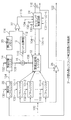
12 受信比較用レジスタ
14 受信対象レジスタ
16、22 比較器
18 ビット加算器
20 誤り許容メモリ
24 タイミング制御回路
26 ゲート回路
28 補正用シフトレジスタ
Claims (6)
- データ取り込みクロックの位相を補正するデータ取り込みクロック補正回路において、該回路は、
復調信号から再生された再生クロックと同じ周期を有し位相が互いに異なる複数のサンプリングクロックを生成し、該複数のサンプリングクロックの一つをデータ取り込みクロックとして選択するタイミング制御手段と、
該タイミング制御手段で生成された複数のサンプリングクロックに従って復調信号をサンプリングし、サンプリングした信号を該複数のサンプリングクロック毎に格納する複数のシフトレジスタからなるオーバーサンプリング手段と、
前記タイミング制御手段で選択されたデータ取り込みクロックに従って復調信号からデータを取り込んで出力するゲート手段と、
該ゲート手段から出力されるデータを受信対象として格納する受信対象格納手段と、
該受信対象格納手段に格納された受信対象と前記オーバーサンプリング手段の複数のシフトレジスタにそれぞれ格納されるデータとを順次比較して不一致ビット数を算出する不一致ビット数算出手段と、
該不一致ビット数算出手段で算出された不一致ビット数と予め定められている誤り許容ビット数を順次比較し、不一致ビット数が誤り許容ビット数より小さくなる期間を検出する比較手段とを含み、
前記タイミング制御手段は、前記不一致ビット数算出手段により算出された期間の中心位置を算出し、該中心位置に対応するサンプリングクロックを前記データ取り込みクロックとして選択することを特徴とするデータ取り込みクロック補正回路。 - 請求項1に記載のデータ取り込みクロック補正回路において、前記受信対象格納手段は、前記オーバーサンプリング手段における複数のシフトレジスタのうち前記データ取り込みクロックに対応するサンプリングクロックが供給されるシフトレジスタに格納された信号を受信対象として格納すること特徴とするデータ取り込みクロック補正回路。
- 請求項1または2に記載のデータ取り込みクロック補正回路において、前記タイミング制御手段は、復調信号に含まれる受信データが入力さる期間において1または複数回、前記複数のサンプリングクロックを生成して出力することを特徴とするデータ取り込みクロック補正回路。
- 請求項1または2に記載のデータ取り込みクロック補正回路において、前記タイミング制御手段は、前記再生クロックとデータ取り込みクロックの位相差を検出し、位相差が予め定められた閾値を超えたとき前記複数のサンプリングクロックを生成して出力することを特徴とするデータ取り込みクロック補正回路。
- 請求項1または2に記載のデータ取り込みクロック補正回路において、復調信号に含まれる機器間識別信号が入力される期間、前記受信対象格納手段は所望の機器間識別信号を格納し、前記タイミング制御手段は前記複数のサンプリングクロックを生成して出力することを特徴とするデータ取り込みクロック補正回路。
- 請求項5に記載のデータ取り込みクロック補正回路において、前記機器間識別信号は同期パターンであることを特徴とするデータ取り込みクロック補正回路。
Priority Applications (2)
| Application Number | Priority Date | Filing Date | Title |
|---|---|---|---|
| JP2004011477A JP4274469B2 (ja) | 2004-01-20 | 2004-01-20 | データ取り込みクロック補正回路 |
| US11/038,061 US7167034B2 (en) | 2004-01-20 | 2005-01-21 | Arrangement for correcting the phase of a data sampling clock signal during a period of sampling data in a received signal |
Applications Claiming Priority (1)
| Application Number | Priority Date | Filing Date | Title |
|---|---|---|---|
| JP2004011477A JP4274469B2 (ja) | 2004-01-20 | 2004-01-20 | データ取り込みクロック補正回路 |
Publications (3)
| Publication Number | Publication Date |
|---|---|
| JP2005210162A JP2005210162A (ja) | 2005-08-04 |
| JP2005210162A5 JP2005210162A5 (ja) | 2006-09-21 |
| JP4274469B2 true JP4274469B2 (ja) | 2009-06-10 |
Family
ID=34747292
Family Applications (1)
| Application Number | Title | Priority Date | Filing Date |
|---|---|---|---|
| JP2004011477A Expired - Fee Related JP4274469B2 (ja) | 2004-01-20 | 2004-01-20 | データ取り込みクロック補正回路 |
Country Status (2)
| Country | Link |
|---|---|
| US (1) | US7167034B2 (ja) |
| JP (1) | JP4274469B2 (ja) |
Families Citing this family (7)
| Publication number | Priority date | Publication date | Assignee | Title |
|---|---|---|---|---|
| US20060176934A1 (en) * | 2005-02-07 | 2006-08-10 | Inova Semiconductors Gmbh | Serial transmission of data using spread-spectrum modulation for enhancing electromagnetic compatibility |
| JP2007067646A (ja) * | 2005-08-30 | 2007-03-15 | Oki Electric Ind Co Ltd | サンプリングレート変換方法及びその回路 |
| US8428195B2 (en) * | 2007-12-31 | 2013-04-23 | Agere Systems Llc | Methods and apparatus for detecting and decoding adaptive equalization training frames |
| US8094766B2 (en) * | 2008-07-02 | 2012-01-10 | Teradyne, Inc. | Tracker circuit and method for automated test equipment systems |
| JP5418035B2 (ja) * | 2009-07-21 | 2014-02-19 | 富士ゼロックス株式会社 | 直列信号の受信装置、直列信号の受信方法、直列伝送システムおよび画像形成装置 |
| JP7148796B2 (ja) * | 2018-12-11 | 2022-10-06 | 日本電信電話株式会社 | 伝送装置及び伝送システム |
| CN112511164B (zh) * | 2020-11-25 | 2023-03-14 | 中国科学技术大学 | 基于单比特采样的高速实时弱信号检测方法及装置 |
Family Cites Families (4)
| Publication number | Priority date | Publication date | Assignee | Title |
|---|---|---|---|---|
| ATE244570T1 (de) * | 1993-09-09 | 2003-07-15 | Lorus Therapeutics Inc | Immunmodulierende zusammensetzungen aus galle |
| JPH0898284A (ja) * | 1994-07-25 | 1996-04-12 | Nippondenso Co Ltd | データ受信装置,送信装置および通信装置 |
| EP0821503B1 (en) * | 1996-07-22 | 2007-01-03 | Nippon Telegraph And Telephone Corporation | Clock timing recovery circuit |
| JP3262219B2 (ja) | 1998-05-27 | 2002-03-04 | エヌイーシーアクセステクニカ株式会社 | 無線通信装置及びその同期引き込み方法 |
-
2004
- 2004-01-20 JP JP2004011477A patent/JP4274469B2/ja not_active Expired - Fee Related
-
2005
- 2005-01-21 US US11/038,061 patent/US7167034B2/en not_active Expired - Fee Related
Also Published As
| Publication number | Publication date |
|---|---|
| JP2005210162A (ja) | 2005-08-04 |
| US20050156645A1 (en) | 2005-07-21 |
| US7167034B2 (en) | 2007-01-23 |
Similar Documents
| Publication | Publication Date | Title |
|---|---|---|
| US8842793B2 (en) | Communication circuit and method of adjusting sampling clock signal | |
| EP0877505B1 (en) | Synchronous circuit controller for controlling data transmission between asynchronous circuits | |
| EP1434057A2 (en) | Frequency detection circuit and data processing apparatus | |
| JP2011234128A (ja) | シリアル通信用ボーレート検出装置およびシリアル通信用ボーレート補正装置ならびにシリアル通信用ボーレート検出方法 | |
| CN112104435B (zh) | 一种时钟延时补偿方法、逻辑装置及网络设备 | |
| JP4274469B2 (ja) | データ取り込みクロック補正回路 | |
| US20110026572A1 (en) | Baud rate error detection circuit and baud rate error detection method | |
| KR101076109B1 (ko) | 패턴 삽입을 이용한 수신 데이터의 스큐 보정 방법 및 그 장치 | |
| US20120014427A1 (en) | Methods and Apparatus for Determining a Phase Error in Signals | |
| JP2003208400A (ja) | クロック切替回路 | |
| EP3872995A1 (en) | Metastable state detection device and method, and adc circuit | |
| KR101515360B1 (ko) | 저 레이턴시 직렬 상호 접속 아키텍처에서의 피드백 루프의 제공 | |
| US20050047539A1 (en) | Data recovery algorithm using data position detection and serial data receiver adopting the same | |
| JP4599247B2 (ja) | シンボル検出装置、シンボル検出方法、シンボル検出制御プログラム及び記録媒体 | |
| JP2003134098A (ja) | シリアル受信装置 | |
| JP2004310544A (ja) | 非同期データ転送装置 | |
| US7486753B2 (en) | Synchronization establishment circuit and synchronization establishment method | |
| JP4593677B2 (ja) | クロック乗せ換え装置及びクロック乗せ換え方法 | |
| US20090232266A1 (en) | Signal processing device | |
| JP6738028B2 (ja) | 受信回路及び半導体集積回路 | |
| JP2010213204A (ja) | データ送受信方法 | |
| JP2011223391A (ja) | 半導体集積回路およびそれを備えた撮像システム | |
| US6925111B2 (en) | Data communication method and communication control apparatus | |
| JP4826352B2 (ja) | フレームタイミング位相差補正方法および装置 | |
| KR100684564B1 (ko) | 프레임 동기화 방법, 장치 및 이를 위한 기록매체 |
Legal Events
| Date | Code | Title | Description |
|---|---|---|---|
| A521 | Written amendment |
Free format text: JAPANESE INTERMEDIATE CODE: A523 Effective date: 20060808 |
|
| A621 | Written request for application examination |
Free format text: JAPANESE INTERMEDIATE CODE: A621 Effective date: 20060808 |
|
| A977 | Report on retrieval |
Free format text: JAPANESE INTERMEDIATE CODE: A971007 Effective date: 20081029 |
|
| A711 | Notification of change in applicant |
Free format text: JAPANESE INTERMEDIATE CODE: A712 Effective date: 20081126 |
|
| TRDD | Decision of grant or rejection written | ||
| A01 | Written decision to grant a patent or to grant a registration (utility model) |
Free format text: JAPANESE INTERMEDIATE CODE: A01 Effective date: 20090203 |
|
| A01 | Written decision to grant a patent or to grant a registration (utility model) |
Free format text: JAPANESE INTERMEDIATE CODE: A01 |
|
| RD02 | Notification of acceptance of power of attorney |
Free format text: JAPANESE INTERMEDIATE CODE: A7422 Effective date: 20090227 |
|
| A61 | First payment of annual fees (during grant procedure) |
Free format text: JAPANESE INTERMEDIATE CODE: A61 Effective date: 20090227 |
|
| R150 | Certificate of patent or registration of utility model |
Free format text: JAPANESE INTERMEDIATE CODE: R150 |
|
| FPAY | Renewal fee payment (event date is renewal date of database) |
Free format text: PAYMENT UNTIL: 20120313 Year of fee payment: 3 |
|
| LAPS | Cancellation because of no payment of annual fees |