JP4265729B2 - Embossing tool, method of constructing the surface of a workpiece, use of an anodized surface layer and anti-reflective coating - Google Patents
Embossing tool, method of constructing the surface of a workpiece, use of an anodized surface layer and anti-reflective coating Download PDFInfo
- Publication number
- JP4265729B2 JP4265729B2 JP2001580058A JP2001580058A JP4265729B2 JP 4265729 B2 JP4265729 B2 JP 4265729B2 JP 2001580058 A JP2001580058 A JP 2001580058A JP 2001580058 A JP2001580058 A JP 2001580058A JP 4265729 B2 JP4265729 B2 JP 4265729B2
- Authority
- JP
- Japan
- Prior art keywords
- embossing
- hollow chamber
- embossing tool
- tool according
- layer
- Prior art date
- Legal status (The legal status is an assumption and is not a legal conclusion. Google has not performed a legal analysis and makes no representation as to the accuracy of the status listed.)
- Expired - Lifetime
Links
Images
Classifications
-
- B—PERFORMING OPERATIONS; TRANSPORTING
- B29—WORKING OF PLASTICS; WORKING OF SUBSTANCES IN A PLASTIC STATE IN GENERAL
- B29C—SHAPING OR JOINING OF PLASTICS; SHAPING OF MATERIAL IN A PLASTIC STATE, NOT OTHERWISE PROVIDED FOR; AFTER-TREATMENT OF THE SHAPED PRODUCTS, e.g. REPAIRING
- B29C59/00—Surface shaping of articles, e.g. embossing; Apparatus therefor
- B29C59/02—Surface shaping of articles, e.g. embossing; Apparatus therefor by mechanical means, e.g. pressing
-
- B—PERFORMING OPERATIONS; TRANSPORTING
- B30—PRESSES
- B30B—PRESSES IN GENERAL
- B30B15/00—Details of, or accessories for, presses; Auxiliary measures in connection with pressing
- B30B15/06—Platens or press rams
- B30B15/065—Press rams
-
- B—PERFORMING OPERATIONS; TRANSPORTING
- B29—WORKING OF PLASTICS; WORKING OF SUBSTANCES IN A PLASTIC STATE IN GENERAL
- B29C—SHAPING OR JOINING OF PLASTICS; SHAPING OF MATERIAL IN A PLASTIC STATE, NOT OTHERWISE PROVIDED FOR; AFTER-TREATMENT OF THE SHAPED PRODUCTS, e.g. REPAIRING
- B29C59/00—Surface shaping of articles, e.g. embossing; Apparatus therefor
- B29C59/02—Surface shaping of articles, e.g. embossing; Apparatus therefor by mechanical means, e.g. pressing
- B29C59/022—Surface shaping of articles, e.g. embossing; Apparatus therefor by mechanical means, e.g. pressing characterised by the disposition or the configuration, e.g. dimensions, of the embossments or the shaping tools therefor
-
- C—CHEMISTRY; METALLURGY
- C25—ELECTROLYTIC OR ELECTROPHORETIC PROCESSES; APPARATUS THEREFOR
- C25D—PROCESSES FOR THE ELECTROLYTIC OR ELECTROPHORETIC PRODUCTION OF COATINGS; ELECTROFORMING; APPARATUS THEREFOR
- C25D11/00—Electrolytic coating by surface reaction, i.e. forming conversion layers
- C25D11/02—Anodisation
Landscapes
- Engineering & Computer Science (AREA)
- Mechanical Engineering (AREA)
- Chemical & Material Sciences (AREA)
- Chemical Kinetics & Catalysis (AREA)
- Electrochemistry (AREA)
- Materials Engineering (AREA)
- Metallurgy (AREA)
- Organic Chemistry (AREA)
- Shaping Of Tube Ends By Bending Or Straightening (AREA)
- Moulds For Moulding Plastics Or The Like (AREA)
- Shaping Metal By Deep-Drawing, Or The Like (AREA)
- Mounting, Exchange, And Manufacturing Of Dies (AREA)
- Other Surface Treatments For Metallic Materials (AREA)
- Printing Plates And Materials Therefor (AREA)
- Electroplating Methods And Accessories (AREA)
Description
【0001】
本発明は、構築された型押し面を有する型押し具、構築された型押し面を有する型押し具を製造する方法、加工物の表面を構築する方法、及び陽極酸化による開口中空チャンバを具備する表面層の使用に関する。
【0002】
型押しは、加工物にレリーフのような又は構築した表面を製造するための非切断製造方法を構成する。型彫りされ又は構築された型押し面を有する型押し具は、これに使用される。前記型押し面は、加工物の構成される表面に所定の型押し力でプレスされ、又はこれにロールされるので、加工物は、型押し具又は型押し面において塑造され且つ窪んで形成される。かなりの型押し力が使用されることにより、型押し具及び型押し面は、通常金属で作られる。
【0003】
大変精密に構築され、又は浮き彫りにされた型押し面を有する型押し具を製造するには、大変費用がかかる。いわゆる「モスアイ構造」―均等に配置された鶏卵箱のような突起―又はナノメータレンジの精密な溝を形成するために、2つの干渉するレーザー光線を介して感光性物質に照射するために、周期的な明暗度調整による照明パターンを使用することは、経験から公知である。前記照射物質が発展した後、周期的な表面構造は、結果として、種々のレプリカ作成方法を用いる他の材質に、また最終的にはニッケルに、例えば、電気鋳造法によって鋳造される。この種の製造方法は、大変高価であり、均一な表面を構築するためにのみ適している。
【0004】
本発明において、ナノメータレンジは、1000nmより小さい、特に500nmより小さい構造幅を有する型彫り又は構造化を意味することは言うまでもない。前記構造幅は、突起のような個々の構造化要素が繰返されることによる寸法、すなわち、例えば、お互いに隣接する突起又はお互いの窪みの平均距離を示す。
【0005】
前記ナノメータレンジにおいて、型押し具の型押し面を構築するためのリトグラフ法は、制限された方法においてのみ使用することができる。ここで可視光線の波長だけですでに400nm〜750nmあることが示されるべきである。各場合において、リトグラフ法は、大変高価である。
【0006】
独国特許第19727132号は、電解研摩による型押し具の製造を開示する。電解研摩の間、型押し具の金属製の型押し面は電解液で処理され、そこでは、速く流れる電解液内でアノードであり、型押し面の金属は、カソードに対して最小の間隔で配され、表面電極において溶解する。前記金属又は型押し面は、カソードの形状によって決定される構造を有し、これによって、前記カソードは、電気化学的に形成された容器を形成する。また、独国特許第19727132号は、要求された型押し構造のネガ形状を与える被覆表面を有する円筒状の回転電極の使用を提供する。ここでもまた、著しい費用が必要であり、ナノメータレンジで構造化することは、少なくとも部分的にのみ可能である。
【0007】
本発明の目的は、型押し具、型押し具を製造する方法、加工物の表面を構築する方法、及び開口中空チャンバを具備する表面層の使用を提供することであり、ナノメータレンジでの構造化を簡単に且つ費用効果の高い方法で可能にするものである。
【0008】
上記目的は、請求項1に記載の型押し具、請求項10〜15に記載の方法、又は請求項17に記載の使用によって達成される。有益な具体例は、サブクレームに示される。
【0009】
本発明の本質的な概念は、型押し具の型押し面として、多孔性の酸化層、そして特に陽極酸化を介して形成され且つ開口中空チャンバを具備する表面層を使用することである。これは、いくつかの利点を導く。
【0010】
第1に、酸化層、特に好ましく設けられた酸化アルミニウムは、相対的に硬い。頻繁にかかる大変高い型押し力に関して、これは、種々の材質の加工物を型押しすることができ、且つ型押し具の長い金型寿命を達成できるということについて利点を有する。
【0011】
第2に、型のない酸化は大変簡単であり、且つ実現するための費用効率が高い。特に、中空チャンバを製造することは、いわば、使用されるカソードの形状及び配置と無関係なので、模型又はネガ形式は、電解研摩でのように、要求されない。
【0012】
第3に、陽極酸化による開口中空チャンバの提供された型のない形成は、ナノメータレンジで製造される構成を大変簡単に且つ高い費用効率で行うことができる。特に、500nm以下、さらに100nm以下の構造幅が可能となる。
【0013】
第4に、進行状態の選択により、中空チャンバの―規則的又は不規則な―配置及び表面密度は、要求されるように変化させることができる。
【0014】
第5に、同じく単に進行状態を変化させることによって―特に、酸化の間の電圧の変更によって―中空チャンバの形状及びこれによる型押し面の構造を調節し且つ変更することができる。
【0015】
第6に、陽極酸化表面層は、直接的に、これによりさらなる成形作業なしに、型押し具の型押し面として使用することができる。
【0016】
本発明のさらなる利点、特性、特徴及び目的は、図面を参照して好ましい具体例の下記する記載から明らかになるだろう。唯一の図面は、提案された型押し具及びそれによって構築された加工物の概略断面図を示している。
【0017】
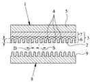
高度に簡略化された断面図において、図面は、構築され、すなわち、型彫り又は浮き彫りのような型押し面2を有する提案された型押し具1を示す。前記型押し面2は、陽極酸化によって形成された開口中空チャンバ4を具備する表面層3のフラット側面によって形成される。
【0018】
図示された例において、表面層は、型押し具1の支持部5に設けられる。例えば、表面層3は、プラズマコーティングによって支持部5に設けられる。しかし、表面層3は、また支持部5によって直接的に形成されることもでき、この場合は、支持部5の表面領域となる。
【0019】
また、表面層3は、他の方法を用いて、支持部5に被覆することもできることは言うまでもない。
【0020】
図示された例において、表面層3は、特にプラズマコーティングによって支持部5に形成され、好ましくは金属、特に鉄又は鋼から作られる支持部5に対して良好に接着するアルミニウムからなることが好ましい。
【0021】
表面層3は、図示された例において少なくとも部分的に、被覆層6の深さまで陽極酸化され、これによって中空チャンバ4が表面層3に形成される。前記中空チャンバ4はすぐに形成され、且つ/又は、いかなる型又はパターンなしに、いわゆる中空チャンバ4の配置、分布、形状等は―電解研摩に対抗するものとして―酸化に使用されるカソード(図示しない)の表面形状及び近接と、少なくとも本質的に無関係である。さらに、この発明によれば、「バルブ効果」、すなわち表面層3の酸化又は陽極酸化の間生じる中空チャンバ4の自由な構成が―少なくとも、特にいわゆるバルブ金属において―用いられる。中空チャンバ4のこの直接的な又は不確定な構成は、さらなる(前又は後の)構成、又は型押し面2の構造化、又はネガ形式による中空チャンバ4を妨げない。
【0022】
前記表面層3がいかに完全に、又はいかに深く酸化されるかにより、又は前記表面層3が支持部5によって直接的に形成されるかどうかにより、表面層3は、酸化した被覆層6に対応することができる。この場合、例えば、図示された例においては、アルミニウムからなり且つ被覆層6及び支持部5の間の大変良い粘着を増進する中間層7を、省略することができる。
【0023】
例えば、別の例によれば、コートされない支持部5は、多孔性酸化層又は中空チャンバ4の構成によって型押し面2を形成するその表面上に陽極酸化される。例えば、これは、鉄又は鋼、特にステンレス鋼から作られる支持部5について可能となる。そして、この場合、表面層3は、いわゆる酸化層である被覆層6に対応する。
【0024】
アルミニウム及び鉄又は鋼、特にステンレス鋼は、特に好ましい材料としてすでに名前があがっており、陽極酸化表面層3又は被覆層6を形成するのに、少なくとも実質的に使用されていた。しかしながら、例えば他の弁金属と同様に珪素やチタンも使用することができる。
【0025】
図示した例において、寸法の比率は、真実の尺度を示していない。
【0026】
型押し具1又はその型押し面2は、ナノメータレンジ、特に30nm〜600nm、好ましくは50〜200nmの構成幅Sを有することが好ましい。
【0027】
前記中空チャンバ4又はそれらの開口部は、実質的には10〜500nm、好ましくは、15〜200nm、特に20〜100nmの平均直径Dを有する。
【0028】
図示した例において、前記中空チャンバ4は、実質的には縦長に形成され、その深さTは、上述した平均直径Dの少なくとも約0.5倍、特に平均直径Dの約1.0倍〜10倍であることが好ましい。
【0029】
ここで、前記中空チャンバ4は、少なくとも実質的に形状において同様に形成される。特に、前記中空チャンバ4は、実質的に円筒形状に形成される。しかし、前記中空チャンバ4は、その形状からはずれる形状を示してもよく、例えばそれらは実質的に円錐形状に形成される。
【0030】
一般的に、前記中空チャンバ4は、その深さT、形状及び/又は直径において異なる断面を有してもよい。これに加えて、前記中空チャンバ4は、例えば粗い構造として実質的に円錐形状に形成され、且つ、それらの壁部に沿って多くの精密な窪み(小さな中空チャンバ)を具備し、各々の場合において精密な構造を形成する。
【0031】
前記中空チャンバ4は、前記表面層3の表面にわたって、又は型押し面2にわたって、少なくとも実質的に均一に分配されることが好ましい。しかしながら、不均一な分配もまた可能である。
【0032】
前記中空チャンバ又はそれらの開口部は、109〜1011/cm2の表面密度で、型押し面2全体に分配されることが好ましい。図示された例において、表面密度は、型押し面2にわたって実質的に一定である。しかし、表面密度は、要求されるように型押し面2において部分的に変化させることもできる。
【0033】
前記中空チャンバ4の開口部の面積は、最大で、前記型押し面の延長面積の最大50%であることが好ましい。これによって、型押し面2又は表面層3/被覆層6の十分に高い安定性又は負荷容量が、型押しの間に上昇する高い押圧力に関して達成される。
【0034】
一般的に、中空チャンバ4の形状、配置、表面密度等は、陽極酸化の間の進行状態の対応する選択によって制御される。例えば、定電位状態下のアルミニウムの酸化―少なくとも実質的には定電圧―では、前記中空チャンバ4の少なくとも実質的に平滑な断面が、それらの深さT、すなわち少なくとも実質的に円筒形状にわたって達成される。したがって、前記中空チャンバ4の形状は、電圧を変化させることによって影響される。例えば、定電流―すなわち少なくとも実質的に一定の電流での―酸化は、前記中空チャンバ4の円錐形状又は丘状形を導くので、ある種の「モスアイ構造」のようなものが、この方法で形成される。前記中空チャンバ4の表面密度、いわゆる表面上の前記型押し面2の表面単位における中空チャンバの数は、とりわけ酸化の間の電圧及び電流に依存する。
【0035】
要求されるように、中空チャンバ4は、それらの形状、深さ及び/若しくは型押し面2の表面密度において、特に部分的に変化させることができ、且つ/又は、型押し面2においてのみ部分的に形成することができる。
【0036】
そしてまた、もし要求されるならば、型押し面2は、酸化―中空チャンバ4の形成―の前及び/若しくは後で、例えばリトグラフ工程、エッチング及び/若しくは、好ましくは他の材料剥離法によって改造され、型押し面2に、通路、リッジ、中空チャンバのある領域又はないの領域、大きい表面突出又は窪み等の形状において、粗い構造を形成する。
【0037】
特に酸化物質の部分的エッチングによるケミカルサイジングもまた、型押し面2又は中空チャンバ4を改造するために実行することができる。この方法において、型押し面2の延長面積に対する中空チャンバ4の開口面積の表面比率を、変更又は増加することができる。型押し面2又は中空チャンバ4の他の改造もまた、反応時間及び強さによって左右される。
【0038】
また、提示された解決手段の特別な利点は、型押し面2が、曲がった形―例えば円筒形状に―または湾曲されて―例えば凸レンズ状又は半球状に形成されることである。特に、型押し面2は、実際的にいかなる形状をも有するすることができる。これにより、従来技術と比べて、型押し面2又は表面層3/被覆層6の表面は、少なくとも実質的に平らである必要はない。
【0039】
図はまた、同様に、高度に簡略され、寸法が真実でない断面概略図において、既に型押しされた状態において、いわゆる型押し具1によってすでに構築された表面を有する加工物8を示す。型押しは、構築される加工物8の表面9に対して、対応する型押し力でプレスされる型押し具1によって特に行われるために、加工物8の材質は、中空チャンバ4内に少なくとも部分的に流れ込む。ここで、加工物8は、図面に概略的に示されたように、一体鋳造法で形成される必要はない。その代わりとして、加工物8は、表面9を形成し且つ型押し具1によって浮き彫りのような方法で構築され又は形成される、ここで図示されない、別のタイプの表面層又は表面コーティング等を提示することもできる。
【0040】
型押しのような浮き彫り加工の代わりに、型押し具1は、型押し面2及び/若しくは構築される表面9の対応する形状/形態で巻出しされることができる。例によれば、型押し面2及び/若しくは構築される面9は、屈曲した形に―例えば、円筒形に―又は湾曲した形に形成され、表面9を構築するために相互に巻き出すことができる。
【0041】
また、型押し工程及びロール型押し工程は共に、提案された解決手段で実現される。
【0042】
さらにまた、提案された解決手段は、型押しと同様にクローズドダイコイニング又はコイニングに用いることができる。前記加工物8の対応する接合面又は対応するカウンタツールは、明確化の目的のために図示されない。
【0043】
提案された型押し具1は、加工物8又はその表面9を大変精密な構造にする。もし、必要ならば、加工物8又はその表面9は、最初に―任意に慣習的な方法において製造された―粗く構築された型押し具で、そしてそれから、より精密に構成された提案された型押し具で、型彫りされ又は繰り返して構築される。より小さい型押し力が、特に精密な型押し具1を使用する第2の型押し作業の間及び/若しくは中間工程において用いられ、表面9が硬化され、第1の型押しで製造された粗い構成を十分に中和せずに、両方の型押し具の粗い構造及び精密な構造から重ね合わせを達成する。これによって、例えば、加工物8の表面9に、10〜400nmのオーダーの比較的小さい突起を各々が有する0.1〜50μmのオーダーの比較的大きな突出部を形成することができる。
【0044】
大変容易で且つ費用効率の良い提案された解決手段は、表面9を大変精密な構造にすることができる。したがって、応用の大変広範な領域がある。例えば、そのような特別に大変精密な構造化は、反射防止膜において、構築された表面の放射状態を変更するために、感覚分析において、触媒作用において、自己浄化表面において、また表面の湿潤化改善等において用いることができるものである。特に、提案された解決手段は、また上述した目的のために提案された型押し具1の使用によって構築された構造化表面9を有する加工物8の使用にまで拡張される。
【0045】
特に、提案された解決手段は、合成物質の型押し―例えば、PMMA(ポリメチルメタクリレート)、テフロン(登録商標)等、金属―例えば、金、銀、プラチナ、鉛、イジウム、亜鉛等、ポリマーコーティング―例えば、ペイント、染料等、及び無機のコーティング系等に適している。
【0046】
一般的用語において表現すると、本願発明の本質的な様相は、底型又は上型として、陽極酸化によって形成された中空チャンバを有する表面層を使用し、ナノメータレンジで表面を構築することができるということである。
【図面の簡単な説明】
【図1】 図1は、提案された型押し具及びそれで構築された加工物の概略断面図である。[0001]
The present invention comprises an embossing tool having a structured embossing surface, a method for manufacturing a embossing tool having a structured embossing surface, a method for constructing a surface of a workpiece, and an open hollow chamber by anodization. Relates to the use of surface layers.
[0002]
Embossing constitutes a non-cutting manufacturing method for manufacturing a relief-like or constructed surface on a workpiece. A stamping tool with a stamped or constructed stamping surface is used for this. The embossing surface is pressed or rolled onto the surface of the workpiece with a predetermined embossing force, so that the workpiece is formed in the embossing tool or the embossing surface and is recessed. The Due to the considerable embossing force used, the embossing tool and the embossing surface are usually made of metal.
[0003]
It is very expensive to produce a stamping tool with a stamping surface that is very precisely constructed or embossed. The so-called “moth eye structure” —protrusions like an evenly arranged egg box—or periodic to irradiate the photosensitive material via two interfering laser beams to form precise grooves in the nanometer range It is known from experience to use an illumination pattern with an appropriate brightness adjustment. After the irradiation material has developed, the periodic surface structure is consequently cast on other materials using various replica making methods and finally on nickel, for example by electroforming. This type of manufacturing method is very expensive and is only suitable for building a uniform surface.
[0004]
In the context of the present invention, the nanometer range means of course engraving or structuring with a structural width smaller than 1000 nm, in particular smaller than 500 nm. The structure width indicates the dimension by which individual structuring elements such as protrusions are repeated, i.e., for example, the average distance between protrusions adjacent to one another or depressions from one another.
[0005]
In the nanometer range, the lithographic method for constructing the embossing surface of the embossing tool can only be used in a limited way. It should be shown here that the wavelength of visible light alone is already 400 nm to 750 nm. In each case, the lithographic method is very expensive.
[0006]
German Patent No. 19727132 discloses the production of stamping tools by electrolytic polishing. During electropolishing, the metal stamping surface of the stamping tool is treated with electrolyte, where it is the anode in the fast-flowing electrolyte and the metal on the stamping surface is at a minimum distance to the cathode. Dissolved at the surface electrode. The metal or stamping surface has a structure determined by the shape of the cathode, whereby the cathode forms an electrochemically formed container. German Patent No. 19727132 also provides the use of a cylindrical rotating electrode with a coated surface that gives the negative shape of the required embossed structure. Again, significant costs are required and structuring in the nanometer range is only possible at least in part.
[0007]
It is an object of the present invention to provide a mold tool, a method of manufacturing a mold tool, a method of constructing the surface of a workpiece, and the use of a surface layer comprising an open hollow chamber, and a structure in the nanometer range. Is made possible in a simple and cost-effective manner.
[0008]
The object is achieved by a stamping tool according to claim 1, a method according to claims 10-15, or a use according to claim 17. Useful examples are given in the subclaims.
[0009]
The essential concept of the present invention is to use as the embossing surface of the embossing tool a porous oxide layer, and in particular a surface layer formed via anodization and comprising an open hollow chamber. This leads to several advantages.
[0010]
First, the oxide layer, particularly preferably provided aluminum oxide, is relatively hard. For the very high stamping forces that are frequently applied, this has the advantage that workpieces of different materials can be stamped and the long tool life of the stamping tool can be achieved.
[0011]
Second, typeless oxidation is very simple and cost effective to achieve. In particular, since the fabrication of the hollow chamber is independent of the shape and arrangement of the cathode used, a model or negative format is not required, as in electropolishing.
[0012]
Third, the provided moldless formation of the open hollow chamber by anodic oxidation makes it very simple and cost-effective to construct a structure manufactured in the nanometer range. In particular, a structure width of 500 nm or less, and further 100 nm or less is possible.
[0013]
Fourth, depending on the selection of the state of progress, the regular and irregular arrangement and surface density of the hollow chamber can be varied as required.
[0014]
Fifth, it is also possible to adjust and change the shape of the hollow chamber and thereby the structure of the embossing surface, also by simply changing the progress, in particular by changing the voltage during oxidation.
[0015]
Sixth, the anodized surface layer can be used directly as an embossing surface of the embossing tool, thereby without further molding operations.
[0016]
Further advantages, characteristics, features and objects of the present invention will become apparent from the following description of preferred embodiments with reference to the drawings. The only drawing shows a schematic cross-sectional view of the proposed embossing tool and the workpiece constructed thereby.
[0017]
In a highly simplified cross-sectional view, the drawing shows the proposed embossing tool 1, which is constructed, ie having an
[0018]
In the illustrated example, the surface layer is provided on the
[0019]
Moreover, it cannot be overemphasized that the
[0020]
In the illustrated example, the
[0021]
The
[0022]
Depending on how completely or deeply the
[0023]
For example, according to another example, the
[0024]
Aluminum and iron or steel, in particular stainless steel, have already been named as particularly preferred materials and have been used at least substantially to form the
[0025]
In the example shown, the ratio of dimensions does not indicate a true measure.
[0026]
The embossing tool 1 or its
[0027]
Said
[0028]
In the illustrated example, the
[0029]
Here, the
[0030]
In general, the
[0031]
The
[0032]
The hollow chambers or their openings are preferably distributed over the
[0033]
The area of the opening of the
[0034]
In general, the shape, arrangement, surface density, etc. of the
[0035]
As required, the
[0036]
And if required, the
[0037]
Chemical sizing, in particular by partial etching of the oxidizing substance, can also be carried out to retrofit the
[0038]
Also, a particular advantage of the presented solution is that the
[0039]
The figure likewise shows a
[0040]
Instead of embossing such as embossing, the embossing tool 1 can be unwound in a corresponding shape / form of the
[0041]
Both the stamping process and the roll stamping process are realized by the proposed solution.
[0042]
Furthermore, the proposed solution can be used for closed die coining or coining as well as embossing. The corresponding joining surface of the
[0043]
The proposed embossing tool 1 makes the
[0044]
A very easy and cost-effective proposed solution can make the surface 9 a very precise structure. Therefore, there is a very wide range of applications. For example, such extraordinarily precise structuring can be applied in sensory analysis, in catalysis, in self-cleaning surfaces, and in surface wetting, in order to change the radiation state of the constructed surface in antireflection coatings . It can be used for improvement and the like. In particular, the proposed solution is also extended to the use of a
[0045]
In particular, proposed solutions include embossing of synthetic materials—eg PMMA (polymethylmethacrylate), Teflon® etc., metals—eg gold, silver, platinum, lead, iridium, zinc etc., polymer coatings -Suitable for paints, dyes, etc., and inorganic coating systems, for example.
[0046]
Expressed in general terms, the essential aspect of the present invention is that a surface layer with a hollow chamber formed by anodization can be used as the bottom mold or top mold to build a surface in the nanometer range. That is.
[Brief description of the drawings]
FIG. 1 is a schematic cross-sectional view of a proposed embossing tool and a workpiece constructed therewith.
Claims (17)
前記型押し面は、バルブ金属から形成された支持体の表面の少なくとも一部に、または支持体の表面に設けられたバルブ金属から形成された表面層の少なくとも一部に、陽極酸化によって生じた中空チャンバを有する被覆層によって形成されており、
前記被覆層は、前記中空チャンバが10〜500nmの平均直径(D)の開口を有する、且つ/又は前記型押し面の構造幅(S)が30〜600nmである精密な構造と、0.1〜50μmのオーダーの窪みからなる粗い構造とを有し、前記精密な構造は前記粗い構造に重ね合わされており、前記中空チャンバは、円錐状に形成された中空チャンバを含む、型押し具。 In a pressing tool having a pressing surface,
The embossing surface is generated by anodic oxidation on at least part of the surface of the support formed from the valve metal or at least part of the surface layer formed from the valve metal provided on the surface of the support . is formed by the covering layer that have a middle empty chamber,
The coating layer has a precise structure is that the hollow chamber is closed the open mouth of the average diameter of 1 0 to 500 nm (D), and / or the embossed surface structure width (S) is 30 to 600 nm, have a coarse structure consisting of depression of the order of 0.1 to 50 [mu] m, the precise structure is superimposed on the coarse structure, the hollow chamber includes a hollow chamber formed in a conical shape, embossing Ingredients.
前記型押し面は、バルブ金属から形成された支持体の表面の少なくとも一部に、または支持体の表面に設けられたバルブ金属から形成された表面層の少なくとも一部に、陽極酸化によって生じた中空チャンバを有する被覆層によって形成されており、前記被覆層は、前記中空チャンバが10〜500nmの平均直径(D)の開口を有する、且つ/又は前記型押し面の構造幅(S)が30〜600nmである精密な構造と、0.1〜50μmのオーダーの窪みからなる粗い構造とを有し、前記精密な構造は前記粗い構造に重ね合わされており、 The embossing surface is generated by anodic oxidation on at least part of the surface of the support formed from the valve metal or at least part of the surface layer formed from the valve metal provided on the surface of the support. The coating layer is formed of a coating layer having a hollow chamber, and the coating layer has an opening having an average diameter (D) of 10 to 500 nm and / or a structure width (S) of the embossing surface is 30. Having a precise structure of ˜600 nm and a rough structure consisting of depressions on the order of 0.1 to 50 μm, the precise structure being superimposed on the rough structure;
前記中空チャンバを有する前記被覆層は、前記支持体の前記表面の前記少なくとも一部または前記表面層の前記少なくとも一部に対する陽極酸化およびその前後に行われたエッチングを経て形成されている、型押し具。 The coating layer having the hollow chamber is formed by embossing the at least part of the surface of the support or the at least part of the surface layer and etching performed before and after the anodic oxidation. Ingredients.
構築される表面は、請求項1から12のいずれかに記載された型押し具によって構築される方法。 In a method of constructing the surface of a workpiece with a stamping tool having a stamping surface,
Surface to be constructed, how Ru constructed by any crab listed embossing tool of claims 1 to 12.
Applications Claiming Priority (3)
| Application Number | Priority Date | Filing Date | Title |
|---|---|---|---|
| DE10020877.0 | 2000-04-28 | ||
| DE10020877A DE10020877C1 (en) | 2000-04-28 | 2000-04-28 | Stamping tool has a structured stamping surface with an anodically oxidized surface layer or a covering layer having open hollow chambers produced by anodic oxidation |
| PCT/EP2001/004650 WO2001083198A1 (en) | 2000-04-28 | 2001-04-25 | Stamping tool, method for structuring a surface of a workpiece and use of an anodized surface layer |
Related Child Applications (3)
| Application Number | Title | Priority Date | Filing Date |
|---|---|---|---|
| JP2008095737A Division JP5307435B2 (en) | 2000-04-28 | 2008-04-02 | Embossing tool |
| JP2008303127A Division JP4420967B2 (en) | 2000-04-28 | 2008-11-27 | Embossing tool, method for constructing the surface of a workpiece, and antireflection film |
| JP2008303126A Division JP4265816B2 (en) | 2000-04-28 | 2008-11-27 | Manufacturing method of embossing tool |
Publications (2)
| Publication Number | Publication Date |
|---|---|
| JP2003531962A JP2003531962A (en) | 2003-10-28 |
| JP4265729B2 true JP4265729B2 (en) | 2009-05-20 |
Family
ID=7640229
Family Applications (5)
| Application Number | Title | Priority Date | Filing Date |
|---|---|---|---|
| JP2001580058A Expired - Lifetime JP4265729B2 (en) | 2000-04-28 | 2001-04-25 | Embossing tool, method of constructing the surface of a workpiece, use of an anodized surface layer and anti-reflective coating |
| JP2008095737A Expired - Lifetime JP5307435B2 (en) | 2000-04-28 | 2008-04-02 | Embossing tool |
| JP2008303127A Expired - Lifetime JP4420967B2 (en) | 2000-04-28 | 2008-11-27 | Embossing tool, method for constructing the surface of a workpiece, and antireflection film |
| JP2008303126A Expired - Lifetime JP4265816B2 (en) | 2000-04-28 | 2008-11-27 | Manufacturing method of embossing tool |
| JP2009120019A Expired - Lifetime JP5025683B2 (en) | 2000-04-28 | 2009-05-18 | Manufacturing method of embossing tool, embossing tool, and antireflection film |
Family Applications After (4)
| Application Number | Title | Priority Date | Filing Date |
|---|---|---|---|
| JP2008095737A Expired - Lifetime JP5307435B2 (en) | 2000-04-28 | 2008-04-02 | Embossing tool |
| JP2008303127A Expired - Lifetime JP4420967B2 (en) | 2000-04-28 | 2008-11-27 | Embossing tool, method for constructing the surface of a workpiece, and antireflection film |
| JP2008303126A Expired - Lifetime JP4265816B2 (en) | 2000-04-28 | 2008-11-27 | Manufacturing method of embossing tool |
| JP2009120019A Expired - Lifetime JP5025683B2 (en) | 2000-04-28 | 2009-05-18 | Manufacturing method of embossing tool, embossing tool, and antireflection film |
Country Status (16)
| Country | Link |
|---|---|
| EP (1) | EP1289734B1 (en) |
| JP (5) | JP4265729B2 (en) |
| KR (1) | KR20020089527A (en) |
| CN (1) | CN1437528A (en) |
| AT (1) | ATE270954T1 (en) |
| AU (2) | AU5632301A (en) |
| BR (1) | BR0110378A (en) |
| CA (1) | CA2407209A1 (en) |
| DE (2) | DE10020877C1 (en) |
| DK (1) | DK1289734T3 (en) |
| ES (1) | ES2222993T3 (en) |
| NO (1) | NO20025117D0 (en) |
| PL (1) | PL358199A1 (en) |
| PT (1) | PT1289734E (en) |
| RU (1) | RU2002130256A (en) |
| WO (1) | WO2001083198A1 (en) |
Cited By (18)
| Publication number | Priority date | Publication date | Assignee | Title |
|---|---|---|---|---|
| WO2011046114A1 (en) * | 2009-10-14 | 2011-04-21 | シャープ株式会社 | Die and method for manufacturing die, and anti-reflection coating |
| WO2011052652A1 (en) * | 2009-10-28 | 2011-05-05 | シャープ株式会社 | Mold, method for manufacturing a mold, and antireflective film |
| US7938640B2 (en) | 2008-02-27 | 2011-05-10 | Sharp Kabushiki Kaisha | Roller nanoimprint apparatus, mold roller for use in roller nanoimprint apparatus, fixing roller for use in roller nanoimprint apparatus, and production method of nanoimprint sheet |
| USRE43694E1 (en) | 2000-04-28 | 2012-10-02 | Sharp Kabushiki Kaisha | Stamping tool, casting mold and methods for structuring a surface of a work piece |
| WO2015163018A1 (en) | 2014-04-22 | 2015-10-29 | シャープ株式会社 | Synthetic polymer membrane having surface with sterilizing activity, laminate equipped with synthetic polymer membrane, sterilization method utilizing surface of synthetic polymer membrane, method for reactivating surface of synthetic polymer membrane, mold for use in production of synthetic polymer membrane, and method for producing mold |
| US10071175B2 (en) | 2014-04-28 | 2018-09-11 | Sharp Kabushiki Kaisha | Filter and container having microbicidal activity |
| US10107574B2 (en) | 2014-08-07 | 2018-10-23 | Sharp Kabushiki Kaisha | Heat exchanger including fins with surface having bactericidal activity, metallic member with surface having bactericidal activity, method for inhibiting mold growth and sterilization method both using surface of fins of heat exchanger or surface of metallic member, and electrical water boiler, beverage supplier, and lunch box lid all including metallic member |
| EP3459353A1 (en) | 2017-09-26 | 2019-03-27 | Sharp Kabushiki Kaisha | Synthetic polymer film whose surface has microbicidal activity, photocurable resin composition, manufacturing method of synthetic polymer film, and sterilization method with use of surface of synthetic polymer film |
| US10251393B2 (en) | 2014-11-20 | 2019-04-09 | Sharp Kabushiki Kaisha | Synthetic polymer film having surface provided with bactericidal activity |
| US10375953B2 (en) | 2015-07-17 | 2019-08-13 | Sharp Kabushiki Kaisha | Synthetic polymer film having surface that is provided with bactericidal action, and film comprising same |
| US10907019B2 (en) | 2015-06-23 | 2021-02-02 | Sharp Kabushiki Kaisha | Synthetic polymer film provided with surface having sterilizing activity |
| US10934405B2 (en) | 2018-03-15 | 2021-03-02 | Sharp Kabushiki Kaisha | Synthetic polymer film whose surface has microbicidal activity, plastic product which includes synthetic polymer film, sterilization method with use of surface of synthetic polymer film, photocurable resin composition, and manufacturing method of synthetic polymer film |
| US10980255B2 (en) | 2014-12-25 | 2021-04-20 | Sharp Kabushiki Kaisha | Food preservation method, food film, food container, and food handling method |
| US11335831B2 (en) | 2017-03-29 | 2022-05-17 | Sharp Kabushiki Kaisha | Optical device case and optical device |
| US11364673B2 (en) | 2018-02-21 | 2022-06-21 | Sharp Kabushiki Kaisha | Synthetic polymer film and production method of synthetic polymer film |
| US11883999B2 (en) | 2015-09-17 | 2024-01-30 | Sharp Kabushiki Kaisha | Synthetic polymer film provided with surface having sterilizing effect, method for manufacturing synthetic polymer film and sterilization method using surface of synthetic polymer film |
| US12070188B2 (en) | 2018-10-10 | 2024-08-27 | Sharp Kabushiki Kaisha | Endoscope tip cover and endoscope |
| US12108933B2 (en) | 2018-03-30 | 2024-10-08 | Sharp Kabushiki Kaisha | Cover for endoscope distal end part and endoscope |
Families Citing this family (61)
| Publication number | Priority date | Publication date | Assignee | Title |
|---|---|---|---|---|
| DE10154756C1 (en) * | 2001-07-02 | 2002-11-21 | Alcove Surfaces Gmbh | Use of a surface layer or covering layer provided with open hollow chambers by anodic oxidation for structuring a surface of a cast part and/or workpiece |
| FR2811316B1 (en) * | 2000-07-06 | 2003-01-10 | Saint Gobain | TRANSPARENT TEXTURE SUBSTRATE AND METHODS OF OBTAINING SAME |
| JP4647812B2 (en) * | 2001-03-23 | 2011-03-09 | 財団法人神奈川科学技術アカデミー | Method for producing anodized porous alumina |
| DE60225460T2 (en) * | 2001-09-14 | 2009-02-26 | Honda Giken Kogyo K.K. | A pneumatic tire having a sealant layer and method of making the same |
| KR101190657B1 (en) * | 2003-04-21 | 2012-10-15 | 삼성전자주식회사 | Manufacturing method of self-ordered nanochannel-array and manufacturing method of nano dot using the nanochannel-array |
| JP2006053220A (en) * | 2004-08-10 | 2006-02-23 | Olympus Corp | MEMBER HAVING ANTI-REFLECTION PART, FORMING MOLD THEREOF, AND METHOD FOR PRODUCING THE MOLD |
| KR100893251B1 (en) * | 2004-12-03 | 2009-04-17 | 샤프 가부시키가이샤 | Reflection preventing material, optical element, display device, stamper manufacturing method, and reflection preventing material manufacturing method using the stamper |
| US7649198B2 (en) | 2005-12-28 | 2010-01-19 | Industrial Technology Research Institute | Nano-array and fabrication method thereof |
| WO2007144826A2 (en) * | 2006-06-13 | 2007-12-21 | Csem Centre Suisse D'electronique Et De Microtechnique Sa | Pharmaceutical tablets with diffractive microstructure and compression tools for producing such tablets |
| US7713768B2 (en) | 2006-06-14 | 2010-05-11 | Kanagawa Academy Of Science And Technology | Anti-reflective film and production method thereof, and stamper for producing anti-reflective film and production method thereof |
| WO2008001847A1 (en) * | 2006-06-30 | 2008-01-03 | Mitsubishi Rayon Co., Ltd. | Mold, process for manufacturing mold, and process for producing sheet |
| CN101398558B (en) * | 2007-09-27 | 2010-09-08 | 北京京东方光电科技有限公司 | Reflection-permeation array substrate and method for manufacturing same |
| KR101124707B1 (en) * | 2007-10-08 | 2012-03-19 | 재단법인서울대학교산학협력재단 | The formative method of functional nano pattern |
| EP2249330A1 (en) | 2008-02-22 | 2010-11-10 | Sharp Kabushiki Kaisha | Display device |
| US8597767B2 (en) | 2008-03-04 | 2013-12-03 | Sharp Kabushiki Kaisha | Optical element, roller type nanoimprinting apparatus, and process for producing die roll |
| JP5176618B2 (en) * | 2008-03-17 | 2013-04-03 | 株式会社村田製作所 | Imprint mold and imprint method using the same |
| KR101049220B1 (en) * | 2008-04-14 | 2011-07-13 | 한국기계연구원 | Manufacturing method of stamp for imprint lithography |
| CN102016651B (en) | 2008-06-06 | 2013-05-22 | 夏普株式会社 | Antireflection film, optical element provided with antireflection film, stamper, manufacturing method of stamper, and manufacturing method of antireflection film |
| CN101959670B (en) | 2008-12-17 | 2014-12-31 | 夏普株式会社 | Roller-type imprint device, and method for manufacturing imprint sheet |
| RU2444769C1 (en) | 2008-12-25 | 2012-03-10 | Шарп Кабусики Кайся | Liquid reservoir, sighting device for sighting under liquid surface and optical film |
| BRPI0906259A2 (en) | 2008-12-26 | 2018-12-26 | Sharp Kk | Method of making a mold and method of producing an anti-reflection film using the mold. |
| CN102301040B (en) | 2009-01-30 | 2014-10-15 | 夏普株式会社 | Mold, mold manufacturing method and method for manufacturing anti-reflection film using the mold |
| EP2405036B1 (en) | 2009-03-05 | 2017-11-08 | Sharp Kabushiki Kaisha | Mold manufacturing method and electrode structure for use therein |
| RU2482221C1 (en) | 2009-04-09 | 2013-05-20 | Шарп Кабусики Кайся | Mould and method of its making |
| DE102009017424B4 (en) * | 2009-04-15 | 2014-10-23 | Automotive Lighting Reutlingen Gmbh | Attachment optics for a light source and illumination device for a motor vehicle with such an attachment optics |
| JP5063812B2 (en) | 2009-04-24 | 2012-10-31 | シャープ株式会社 | Display device and method of manufacturing antireflection film |
| WO2010125795A1 (en) | 2009-04-30 | 2010-11-04 | シャープ株式会社 | Mold and manufacturing method therefor |
| WO2010143503A1 (en) | 2009-06-12 | 2010-12-16 | シャープ株式会社 | Antireflection film, display device and light transmissive member |
| US9403293B2 (en) | 2009-09-04 | 2016-08-02 | Sharp Kabushiki Kaisha | Method for forming anodized layer, method for producing mold, method for producing antireflective film, and mold and antireflective film |
| JP4796217B2 (en) | 2009-10-09 | 2011-10-19 | シャープ株式会社 | Mold, mold manufacturing method and antireflection film |
| WO2011055757A1 (en) * | 2009-11-06 | 2011-05-12 | シャープ株式会社 | Method for producing die, and die |
| WO2011065429A1 (en) | 2009-11-27 | 2011-06-03 | シャープ株式会社 | Die for moth-eye, and method for producing die for moth-eye and moth-eye structure |
| JP4595044B2 (en) * | 2009-12-16 | 2010-12-08 | 財団法人神奈川科学技術アカデミー | Mold made of anodized porous alumina and method for producing the same |
| WO2011105206A1 (en) | 2010-02-24 | 2011-09-01 | シャープ株式会社 | Die, die production method, and production of antireflection film |
| CN102791453B (en) | 2010-03-08 | 2014-08-06 | 夏普株式会社 | Mold release treatment method, mold, method for producing anti-reflective film, mold release treatment device, and washing/drying device for mold |
| US9108351B2 (en) | 2010-03-09 | 2015-08-18 | Sharp Kabushiki Kaisha | Method for forming anodized layer, method for producing mold and method for producing antireflective film |
| JP2011206938A (en) * | 2010-03-29 | 2011-10-20 | Kanagawa Acad Of Sci & Technol | Mold for thermal imprint, method of manufacturing the mold and method of manufacturing resin material using the mold |
| JP5027346B2 (en) | 2010-03-31 | 2012-09-19 | シャープ株式会社 | Mold, mold manufacturing method, and antireflection film manufacturing method |
| WO2011136229A1 (en) | 2010-04-28 | 2011-11-03 | シャープ株式会社 | Method for forming anodized layer |
| CN102859048B (en) | 2010-04-28 | 2015-07-29 | 夏普株式会社 | The manufacture method of mould and mould |
| BR112012029474A2 (en) | 2010-05-19 | 2017-01-24 | Sharp Kk | matrix inspection method |
| US8999133B2 (en) | 2010-08-30 | 2015-04-07 | Sharp Kabushiki Kaisha | Method for forming anodized layer and mold production method |
| KR101960105B1 (en) * | 2010-09-29 | 2019-03-19 | 니폰 라이트 메탈 컴퍼니 리미티드 | Stamp, article, and method for manufacturing said stamp and article |
| US9133558B2 (en) | 2010-10-08 | 2015-09-15 | Sharp Kabushiki Kaisha | Method for producing anodized film |
| JP5612123B2 (en) | 2010-11-29 | 2014-10-22 | シャープ株式会社 | Light guide, lighting device having light guide, and display device |
| WO2012073820A1 (en) | 2010-11-30 | 2012-06-07 | シャープ株式会社 | Electrode structure, substrate holder, and method for forming anodic oxidation layer |
| JP5615971B2 (en) | 2011-04-01 | 2014-10-29 | シャープ株式会社 | Mold manufacturing method |
| JP5856286B2 (en) | 2012-03-26 | 2016-02-09 | シャープ株式会社 | Mold release processing method and manufacturing method of antireflection film |
| JP5824399B2 (en) * | 2012-03-30 | 2015-11-25 | 富士フイルム株式会社 | Resin mold for nanoimprint and manufacturing method thereof |
| JP5797334B2 (en) | 2012-06-06 | 2015-10-21 | シャープ株式会社 | Mold substrate, mold substrate manufacturing method, mold manufacturing method and mold |
| JP5641085B2 (en) * | 2012-07-30 | 2014-12-17 | 大日本印刷株式会社 | Method for manufacturing antireflection article, and method for manufacturing mold for manufacturing antireflection article |
| US9442222B2 (en) | 2012-07-31 | 2016-09-13 | Dai Nippon Printing Co., Ltd. | Antireflective article, image display device, and production mold for antireflective article |
| KR102111381B1 (en) | 2012-07-31 | 2020-05-15 | 다이니폰 인사츠 가부시키가이샤 | Antireflective article, image display device, production mold for antireflective article, and production method for antireflective article production mold |
| WO2015159797A1 (en) | 2014-04-14 | 2015-10-22 | シャープ株式会社 | Mold, method for producing mold, anti-reflection film and method for producing anti-reflection film |
| DE102014210798A1 (en) * | 2014-06-05 | 2015-12-17 | Fraunhofer-Gesellschaft zur Förderung der angewandten Forschung e.V. | Mold, process for its manufacture and use, and plastic film and plastic component |
| US10695955B2 (en) | 2014-11-06 | 2020-06-30 | Sharp Kabushiki Kaisha | Mold manufacturing method and anti-reflective film manufacturing method |
| US10675788B2 (en) | 2014-11-12 | 2020-06-09 | Sharp Kabushiki Kaisha | Method for producing mold |
| AT517019B1 (en) * | 2015-04-02 | 2017-02-15 | Zkw Group Gmbh | Lighting device and motor vehicle headlights |
| WO2017115670A1 (en) | 2015-12-28 | 2017-07-06 | シャープ株式会社 | Printing intaglio, printing intaglio manufacturing method, print - making method , and print |
| DE102019133656A1 (en) * | 2019-12-10 | 2021-06-10 | HELLA GmbH & Co. KGaA | Lighting device for a motor vehicle and a method for producing such a lighting device |
| CN110983404A (en) * | 2019-12-30 | 2020-04-10 | 江苏乐彩印刷材料有限公司 | Environment-friendly energy-saving CTP (computer to plate) lithographic printing material |
Family Cites Families (16)
| Publication number | Priority date | Publication date | Assignee | Title |
|---|---|---|---|---|
| US4190321A (en) * | 1977-02-18 | 1980-02-26 | Minnesota Mining And Manufacturing Company | Microstructured transmission and reflectance modifying coating |
| JPH0516228A (en) * | 1991-04-15 | 1993-01-26 | Dainippon Printing Co Ltd | Gloss-matt type film |
| JP3004127B2 (en) * | 1992-07-15 | 2000-01-31 | エヌ・イーケムキャット株式会社 | Method for producing porous metal oxide |
| DE69522954T2 (en) * | 1994-11-16 | 2002-05-29 | Kabushiki Kaisha Kobe Seiko Sho (Kobe Steel, Ltd.) | VACUUM CHAMBER MADE OF ALUMINUM OR ITS ALLOYS |
| CH689395A5 (en) * | 1995-03-16 | 1999-03-31 | Alusuisse Lonza Services Ag | Process for the continuous anodic oxidation of strip or wire of aluminum. |
| JPH0967173A (en) * | 1995-08-31 | 1997-03-11 | Univ Tohoku | Production of porous alumina tube |
| JPH09155972A (en) * | 1995-12-12 | 1997-06-17 | Ykk Corp | Water-repellent film and manufacturing method thereof |
| JPH09202979A (en) * | 1996-01-26 | 1997-08-05 | Ngk Insulators Ltd | Embossing method for metal mold |
| JPH1016008A (en) * | 1996-07-02 | 1998-01-20 | Sharp Corp | Mold for plastic molding and injection molding apparatus using the mold |
| DE69738752D1 (en) * | 1996-08-26 | 2008-07-17 | Nippon Telegraph & Telephone | METHOD FOR PRODUCING POROUS, ANODIZED ALUMINUM FILMS |
| DE19701568C1 (en) * | 1997-01-17 | 1998-07-23 | Karlsruhe Forschzent | Structured layer formation for micro-engineered functional system |
| DE19708776C1 (en) * | 1997-03-04 | 1998-06-18 | Fraunhofer Ges Forschung | Anti-reflection coating for glass or plastics panels used in windows, display screens etc. |
| FR2762862B1 (en) * | 1997-04-30 | 1999-07-16 | Guial | METHOD FOR MANUFACTURING A CALENDERING CYLINDER AND SHEETS OF THERMOPLASTIC FILMS OBTAINED BY ROLLING A THERMOPLASTIC RESIN USING SUCH A CYLINDER |
| DE19727132C2 (en) * | 1997-06-26 | 2000-02-03 | Hueck Engraving Gmbh | Method and device for producing an embossed structure on an embossing tool used for the surface shaping of press laminates |
| JP3886082B2 (en) * | 1997-11-12 | 2007-02-28 | キヤノン株式会社 | Nanostructure and manufacturing method thereof |
| JP2000071290A (en) * | 1998-08-28 | 2000-03-07 | Teijin Ltd | Method for manufacturing anti-reflective article |
-
2000
- 2000-04-28 DE DE10020877A patent/DE10020877C1/en not_active Expired - Fee Related
-
2001
- 2001-04-25 EP EP01929602A patent/EP1289734B1/en not_active Expired - Lifetime
- 2001-04-25 PT PT01929602T patent/PT1289734E/en unknown
- 2001-04-25 WO PCT/EP2001/004650 patent/WO2001083198A1/en not_active Ceased
- 2001-04-25 ES ES01929602T patent/ES2222993T3/en not_active Expired - Lifetime
- 2001-04-25 PL PL01358199A patent/PL358199A1/en unknown
- 2001-04-25 JP JP2001580058A patent/JP4265729B2/en not_active Expired - Lifetime
- 2001-04-25 CA CA002407209A patent/CA2407209A1/en not_active Abandoned
- 2001-04-25 AT AT01929602T patent/ATE270954T1/en not_active IP Right Cessation
- 2001-04-25 RU RU2002130256/02A patent/RU2002130256A/en not_active Application Discontinuation
- 2001-04-25 CN CN01811497A patent/CN1437528A/en active Pending
- 2001-04-25 DK DK01929602T patent/DK1289734T3/en active
- 2001-04-25 DE DE50102858T patent/DE50102858D1/en not_active Expired - Lifetime
- 2001-04-25 AU AU5632301A patent/AU5632301A/en active Pending
- 2001-04-25 BR BR0110378-4A patent/BR0110378A/en not_active IP Right Cessation
- 2001-04-25 KR KR1020027014341A patent/KR20020089527A/en not_active Withdrawn
- 2001-04-25 AU AU2001256323A patent/AU2001256323B2/en not_active Ceased
-
2002
- 2002-10-24 NO NO20025117A patent/NO20025117D0/en not_active Application Discontinuation
-
2008
- 2008-04-02 JP JP2008095737A patent/JP5307435B2/en not_active Expired - Lifetime
- 2008-11-27 JP JP2008303127A patent/JP4420967B2/en not_active Expired - Lifetime
- 2008-11-27 JP JP2008303126A patent/JP4265816B2/en not_active Expired - Lifetime
-
2009
- 2009-05-18 JP JP2009120019A patent/JP5025683B2/en not_active Expired - Lifetime
Cited By (36)
| Publication number | Priority date | Publication date | Assignee | Title |
|---|---|---|---|---|
| USRE46606E1 (en) | 2000-04-28 | 2017-11-14 | Sharp Kabushiki Kaisha | Stamping tool, casting mold and methods for structuring a surface of a work piece |
| USRE43694E1 (en) | 2000-04-28 | 2012-10-02 | Sharp Kabushiki Kaisha | Stamping tool, casting mold and methods for structuring a surface of a work piece |
| USRE44830E1 (en) | 2000-04-28 | 2014-04-08 | Sharp Kabushiki Kaisha | Stamping tool, casting mold and methods for structuring a surface of a work piece |
| US7938640B2 (en) | 2008-02-27 | 2011-05-10 | Sharp Kabushiki Kaisha | Roller nanoimprint apparatus, mold roller for use in roller nanoimprint apparatus, fixing roller for use in roller nanoimprint apparatus, and production method of nanoimprint sheet |
| US8673193B2 (en) | 2008-02-27 | 2014-03-18 | Sharp Kabushiki Kaisha | Roller nanoimprint apparatus, mold roller for use in roller nanoimprint apparatus, fixing roller for use in roller nanoimprint apparatus, and production method of nanoimprint sheet |
| JPWO2011046114A1 (en) * | 2009-10-14 | 2013-03-07 | シャープ株式会社 | Mold, mold manufacturing method and antireflection film |
| RU2497980C1 (en) * | 2009-10-14 | 2013-11-10 | Шарп Кабусики Кайся | Stamp, and stamp manufacturing method, and antireflection coating |
| WO2011046114A1 (en) * | 2009-10-14 | 2011-04-21 | シャープ株式会社 | Die and method for manufacturing die, and anti-reflection coating |
| US9416461B2 (en) | 2009-10-14 | 2016-08-16 | Sharp Kabushiki Kaisha | Die and method for manufacturing die, and anti-reflection coating |
| WO2011052652A1 (en) * | 2009-10-28 | 2011-05-05 | シャープ株式会社 | Mold, method for manufacturing a mold, and antireflective film |
| JP4916597B2 (en) * | 2009-10-28 | 2012-04-11 | シャープ株式会社 | Mold, mold manufacturing method and antireflection film |
| US9366785B2 (en) | 2009-10-28 | 2016-06-14 | Sharp Kabushiki Kaisha | Mold, method for manufacturing a mold, and antireflective film |
| US10136638B2 (en) | 2014-04-22 | 2018-11-27 | Sharp Kabushiki Kaisha | Synthetic polymer film whose surface has microbicidal activity, multilayer structure having synthetic polymer film, sterilization method with the use of surface of synthetic polymer film, method for reactivating surface of synthetic polymer film, mold for production of synthetic polymer film, and mold manufacturing method |
| US10278387B2 (en) | 2014-04-22 | 2019-05-07 | Sharp Kabushiki Kaisha | Synthetic polymer film whose surface has microbicidal activity, multilayer structure having synthetic polymer film, sterilization method with the use of surface of synthetic polymer film, method for reactivating surface of synthetic polymer film, mold for production of synthetic polymer film, and mold manufacturing method |
| US9781926B2 (en) | 2014-04-22 | 2017-10-10 | Sharp Kabushiki Kaisha | Synthetic polymer film whose surface has microbicidal activity, multilayer structure having synthetic polymer film, sterilization method with the use of surface of synthetic polymer film, method for reactivating surface of synthetic polymer film, mold for production of synthetic polymer film, and mold manufacturing method |
| US9781925B2 (en) | 2014-04-22 | 2017-10-10 | Sharp Kabushiki Kaisha | Synthetic polymer film whose surface has microbicidal activity, multilayer structure having synthetic polymer film, sterilization method with the use of surface of synthetic polymer film, method for reactivating surface of synthetic polymer film, mold for production of synthetic polymer film, and mold manufacturing method |
| US11641854B2 (en) | 2014-04-22 | 2023-05-09 | Sharp Kabushiki Kaisha | Synthetic polymer film whose surface has microbicidal activity, multilayer structure having synthetic polymer film, sterilization method with the use of surface of synthetic polymer film, method for reactivating surface of synthetic polymer film, mold for production of synthetic polymer film, and mold manufacturing method |
| WO2015163018A1 (en) | 2014-04-22 | 2015-10-29 | シャープ株式会社 | Synthetic polymer membrane having surface with sterilizing activity, laminate equipped with synthetic polymer membrane, sterilization method utilizing surface of synthetic polymer membrane, method for reactivating surface of synthetic polymer membrane, mold for use in production of synthetic polymer membrane, and method for producing mold |
| US11638423B2 (en) | 2014-04-22 | 2023-05-02 | Sharp Kabushiki Kaisha | Synthetic polymer film whose surface has microbicidal activity, multilayer structure having synthetic polymer film, sterilization method with the use of surface of synthetic polymer film, method for reactivating surface of synthetic polymer film, mold for production of synthetic polymer film, and mold manufacturing method |
| US9781924B2 (en) | 2014-04-22 | 2017-10-10 | Sharp Kabushiki Kaisha | Synthetic polymer film whose surface has microbicidal activity, multilayer structure having synthetic polymer film, sterilization method with the use of surface of synthetic polymer film, method for reactivating surface of synthetic polymer film, mold for production of synthetic polymer film, and mold manufacturing method |
| US10071175B2 (en) | 2014-04-28 | 2018-09-11 | Sharp Kabushiki Kaisha | Filter and container having microbicidal activity |
| US11280563B2 (en) | 2014-08-07 | 2022-03-22 | Sharp Kabushiki Kaisha | Heat exchanger including fins with surface having bactericidal activity, metallic member with surface having bactericidal activity, method for inhibiting mold growth and sterilization method both using surface of fins of heat exchanger or surface of metallic member, and electrical water boiler, beverage supplier, and lunch box lid all including metallic member |
| US10107574B2 (en) | 2014-08-07 | 2018-10-23 | Sharp Kabushiki Kaisha | Heat exchanger including fins with surface having bactericidal activity, metallic member with surface having bactericidal activity, method for inhibiting mold growth and sterilization method both using surface of fins of heat exchanger or surface of metallic member, and electrical water boiler, beverage supplier, and lunch box lid all including metallic member |
| US10251393B2 (en) | 2014-11-20 | 2019-04-09 | Sharp Kabushiki Kaisha | Synthetic polymer film having surface provided with bactericidal activity |
| US10980255B2 (en) | 2014-12-25 | 2021-04-20 | Sharp Kabushiki Kaisha | Food preservation method, food film, food container, and food handling method |
| US10907019B2 (en) | 2015-06-23 | 2021-02-02 | Sharp Kabushiki Kaisha | Synthetic polymer film provided with surface having sterilizing activity |
| US10375953B2 (en) | 2015-07-17 | 2019-08-13 | Sharp Kabushiki Kaisha | Synthetic polymer film having surface that is provided with bactericidal action, and film comprising same |
| US11883999B2 (en) | 2015-09-17 | 2024-01-30 | Sharp Kabushiki Kaisha | Synthetic polymer film provided with surface having sterilizing effect, method for manufacturing synthetic polymer film and sterilization method using surface of synthetic polymer film |
| US11335831B2 (en) | 2017-03-29 | 2022-05-17 | Sharp Kabushiki Kaisha | Optical device case and optical device |
| EP3459353A1 (en) | 2017-09-26 | 2019-03-27 | Sharp Kabushiki Kaisha | Synthetic polymer film whose surface has microbicidal activity, photocurable resin composition, manufacturing method of synthetic polymer film, and sterilization method with use of surface of synthetic polymer film |
| KR20190035594A (en) | 2017-09-26 | 2019-04-03 | 샤프 가부시키가이샤 | Synthetic polymer film whose surface has microbicidal activity, photocurable resin composition, method for manufacturing a synthetic polymer film, and sterilization method with the use of surface of synthetic polymer film |
| US10968292B2 (en) | 2017-09-26 | 2021-04-06 | Sharp Kabushiki Kaisha | Synthetic polymer film whose surface has microbicidal activity, photocurable resin composition, manufacturing method of synthetic polymer film, and sterilization method with use of surface of synthetic polymer film |
| US11364673B2 (en) | 2018-02-21 | 2022-06-21 | Sharp Kabushiki Kaisha | Synthetic polymer film and production method of synthetic polymer film |
| US10934405B2 (en) | 2018-03-15 | 2021-03-02 | Sharp Kabushiki Kaisha | Synthetic polymer film whose surface has microbicidal activity, plastic product which includes synthetic polymer film, sterilization method with use of surface of synthetic polymer film, photocurable resin composition, and manufacturing method of synthetic polymer film |
| US12108933B2 (en) | 2018-03-30 | 2024-10-08 | Sharp Kabushiki Kaisha | Cover for endoscope distal end part and endoscope |
| US12070188B2 (en) | 2018-10-10 | 2024-08-27 | Sharp Kabushiki Kaisha | Endoscope tip cover and endoscope |
Also Published As
| Publication number | Publication date |
|---|---|
| AU5632301A (en) | 2001-11-12 |
| AU2001256323B2 (en) | 2004-08-05 |
| JP4265816B2 (en) | 2009-05-20 |
| JP4420967B2 (en) | 2010-02-24 |
| WO2001083198A1 (en) | 2001-11-08 |
| DE50102858D1 (en) | 2004-08-19 |
| JP2003531962A (en) | 2003-10-28 |
| DE10020877C1 (en) | 2001-10-25 |
| ATE270954T1 (en) | 2004-07-15 |
| JP2009052147A (en) | 2009-03-12 |
| EP1289734A1 (en) | 2003-03-12 |
| CA2407209A1 (en) | 2002-10-23 |
| NO20025117L (en) | 2002-10-24 |
| RU2002130256A (en) | 2004-05-27 |
| JP2009191368A (en) | 2009-08-27 |
| JP5025683B2 (en) | 2012-09-12 |
| DK1289734T3 (en) | 2004-10-25 |
| PL358199A1 (en) | 2004-08-09 |
| JP2009041116A (en) | 2009-02-26 |
| JP5307435B2 (en) | 2013-10-02 |
| KR20020089527A (en) | 2002-11-29 |
| BR0110378A (en) | 2003-02-04 |
| NO20025117D0 (en) | 2002-10-24 |
| PT1289734E (en) | 2004-10-29 |
| CN1437528A (en) | 2003-08-20 |
| JP2008248388A (en) | 2008-10-16 |
| EP1289734B1 (en) | 2004-07-14 |
| ES2222993T3 (en) | 2005-02-16 |
Similar Documents
| Publication | Publication Date | Title |
|---|---|---|
| JP4265729B2 (en) | Embossing tool, method of constructing the surface of a workpiece, use of an anodized surface layer and anti-reflective coating | |
| USRE43694E1 (en) | Stamping tool, casting mold and methods for structuring a surface of a work piece | |
| Landolt et al. | Electrochemical micromachining, polishing and surface structuring of metals: fundamental aspects and new developments | |
| JP3714507B2 (en) | Method for producing porous anodized alumina film | |
| TW201018952A (en) | Optical element molding die and method for molding optical element | |
| JP3389546B2 (en) | Printing plate support and method for producing the same | |
| KR101165396B1 (en) | Forming method of nano structure using the metal nano ring pattern | |
| JP2017539092A (en) | Method for producing electrode film for capacitor, electrode film and capacitor using this electrode film | |
| US20180016696A1 (en) | Method for dye-free coloring of one-time anodic aluminum oxide surface | |
| US5366613A (en) | Method of electrochemical fine processing | |
| CN107148335B (en) | Manufacturing method of mold and manufacturing method of antireflection film | |
| Gutierrez-Rivera et al. | Metallic submicrometer sieves fabricated by interferometric lithography and electroforming | |
| DE10154756C1 (en) | Use of a surface layer or covering layer provided with open hollow chambers by anodic oxidation for structuring a surface of a cast part and/or workpiece | |
| JP2002069695A (en) | Surface treated aluminum material and method of manufacturing the same | |
| RU97113581A (en) | METHOD FOR PRODUCING A RELIEF POROUS BASIS OF A HYDROGEN ELECTRODE OF A CHEMICAL CURRENT SOURCE | |
| JP2006022365A (en) | Method for producing aluminum foil for electrolytic capacitor electrode | |
| JP2016112796A (en) | Micro-pattern body having nano-pattern structure, and method for manufacturing the same | |
| KR102447305B1 (en) | Electroplating type roller manufacturing method that expresses nano-scale patterns | |
| JP2007262510A (en) | Method of manufacturing nanohole structure | |
| KR20110050299A (en) | Method for producing metal nanoring pattern and method for manufacturing nanostructure using same | |
| JPS5847473B2 (en) | Surface treatment method for aluminum or aluminum alloy | |
| CH687512A5 (en) | Surface layer structuring | |
| WO2006077743A1 (en) | Decorative material and process for producing the same | |
| JP2004050693A (en) | Mold and its manufacturing method |
Legal Events
| Date | Code | Title | Description |
|---|---|---|---|
| A621 | Written request for application examination |
Free format text: JAPANESE INTERMEDIATE CODE: A621 Effective date: 20041104 |
|
| A131 | Notification of reasons for refusal |
Free format text: JAPANESE INTERMEDIATE CODE: A131 Effective date: 20071009 |
|
| A601 | Written request for extension of time |
Free format text: JAPANESE INTERMEDIATE CODE: A601 Effective date: 20071228 |
|
| A602 | Written permission of extension of time |
Free format text: JAPANESE INTERMEDIATE CODE: A602 Effective date: 20080110 |
|
| A601 | Written request for extension of time |
Free format text: JAPANESE INTERMEDIATE CODE: A601 Effective date: 20080117 |
|
| A602 | Written permission of extension of time |
Free format text: JAPANESE INTERMEDIATE CODE: A602 Effective date: 20080124 |
|
| A521 | Request for written amendment filed |
Free format text: JAPANESE INTERMEDIATE CODE: A523 Effective date: 20080402 |
|
| A711 | Notification of change in applicant |
Free format text: JAPANESE INTERMEDIATE CODE: A711 Effective date: 20080605 |
|
| RD02 | Notification of acceptance of power of attorney |
Free format text: JAPANESE INTERMEDIATE CODE: A7422 Effective date: 20080616 |
|
| RD04 | Notification of resignation of power of attorney |
Free format text: JAPANESE INTERMEDIATE CODE: A7424 Effective date: 20080623 |
|
| A521 | Request for written amendment filed |
Free format text: JAPANESE INTERMEDIATE CODE: A821 Effective date: 20080606 |
|
| A02 | Decision of refusal |
Free format text: JAPANESE INTERMEDIATE CODE: A02 Effective date: 20080930 |
|
| A521 | Request for written amendment filed |
Free format text: JAPANESE INTERMEDIATE CODE: A523 Effective date: 20081127 |
|
| A911 | Transfer to examiner for re-examination before appeal (zenchi) |
Free format text: JAPANESE INTERMEDIATE CODE: A911 Effective date: 20081210 |
|
| A131 | Notification of reasons for refusal |
Free format text: JAPANESE INTERMEDIATE CODE: A131 Effective date: 20090120 |
|
| A521 | Request for written amendment filed |
Free format text: JAPANESE INTERMEDIATE CODE: A523 Effective date: 20090122 |
|
| TRDD | Decision of grant or rejection written | ||
| A01 | Written decision to grant a patent or to grant a registration (utility model) |
Free format text: JAPANESE INTERMEDIATE CODE: A01 Effective date: 20090210 |
|
| A01 | Written decision to grant a patent or to grant a registration (utility model) |
Free format text: JAPANESE INTERMEDIATE CODE: A01 |
|
| A61 | First payment of annual fees (during grant procedure) |
Free format text: JAPANESE INTERMEDIATE CODE: A61 Effective date: 20090210 |
|
| R150 | Certificate of patent or registration of utility model |
Ref document number: 4265729 Country of ref document: JP Free format text: JAPANESE INTERMEDIATE CODE: R150 Free format text: JAPANESE INTERMEDIATE CODE: R150 |
|
| FPAY | Renewal fee payment (event date is renewal date of database) |
Free format text: PAYMENT UNTIL: 20120227 Year of fee payment: 3 |
|
| FPAY | Renewal fee payment (event date is renewal date of database) |
Free format text: PAYMENT UNTIL: 20120227 Year of fee payment: 3 |
|
| FPAY | Renewal fee payment (event date is renewal date of database) |
Free format text: PAYMENT UNTIL: 20130227 Year of fee payment: 4 |
|
| FPAY | Renewal fee payment (event date is renewal date of database) |
Free format text: PAYMENT UNTIL: 20130227 Year of fee payment: 4 |
|
| FPAY | Renewal fee payment (event date is renewal date of database) |
Free format text: PAYMENT UNTIL: 20140227 Year of fee payment: 5 |
|
| EXPY | Cancellation because of completion of term |