JP4265722B2 - Pattern data correction method and apparatus - Google Patents
Pattern data correction method and apparatus Download PDFInfo
- Publication number
- JP4265722B2 JP4265722B2 JP2000238152A JP2000238152A JP4265722B2 JP 4265722 B2 JP4265722 B2 JP 4265722B2 JP 2000238152 A JP2000238152 A JP 2000238152A JP 2000238152 A JP2000238152 A JP 2000238152A JP 4265722 B2 JP4265722 B2 JP 4265722B2
- Authority
- JP
- Japan
- Prior art keywords
- graphic data
- data
- size
- pattern
- graphic
- Prior art date
- Legal status (The legal status is an assumption and is not a legal conclusion. Google has not performed a legal analysis and makes no representation as to the accuracy of the status listed.)
- Expired - Fee Related
Links
Images
Classifications
-
- G—PHYSICS
- G06—COMPUTING OR CALCULATING; COUNTING
- G06F—ELECTRIC DIGITAL DATA PROCESSING
- G06F30/00—Computer-aided design [CAD]
- G06F30/30—Circuit design
- G06F30/39—Circuit design at the physical level
- G06F30/398—Design verification or optimisation, e.g. using design rule check [DRC], layout versus schematics [LVS] or finite element methods [FEM]
Landscapes
- Engineering & Computer Science (AREA)
- Computer Hardware Design (AREA)
- Physics & Mathematics (AREA)
- Theoretical Computer Science (AREA)
- Evolutionary Computation (AREA)
- Geometry (AREA)
- General Engineering & Computer Science (AREA)
- General Physics & Mathematics (AREA)
- Design And Manufacture Of Integrated Circuits (AREA)
- Preparing Plates And Mask In Photomechanical Process (AREA)
Description
【0001】
【発明の属する技術分野】
本発明は、設計された回路のパターンデータを修正するパターンデータ修正方法及び装置に関する。
【0002】
【従来の技術】
半導体集積回路の多機能化及びパターン高密度化に伴い、設計データ量が増大する傾向にあり、設計されたパターンデータの修正を短時間で行なうことが要求されている。
【0003】
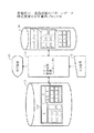
図6は、半導体集積回路の設計データのセル配置を視覚的に示す概略ブロック図である。
【0004】
例えば、半導体集積回路メーカは、チップ全体のセルTOPのうちセルC〜Fを設計し、外部のある会社にセルAの設計を依頼し、他の会社にセルBの設計を依頼し、出来上がったセルA及びBをセルTOP内に配置する。一般に、設計されたセルTOP、A及びBのCADデータのフォーマットは互いに異なり、セルA及びBをセルTOP内に配置する際にこれらのフォーマットが統一されたフォーマット、例えばGDS2フォーマットに変換される。セルTOP、A及びBの中のセル名はそれぞれ独立に付けられており、例えばセルTOP内のセルCとセルA内のセルCとは、セル名が同一であってもその内容は異なる。
【0005】
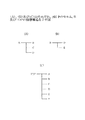
図8(A)、(B)及び(C)はそれぞれ、図6中のセルA、B及びTOPの階層構造を示す。実際にはこれらの階層構造は複雑であるが、説明上、簡単なものが示されている。
【0006】
セルA及びBをセルTOP内に配置する際、一般にフォーマットが互いに異なるので、セルA及びB内が展開されて階層構造が無くなる。
【0007】
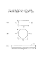
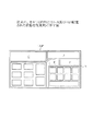
図7は、セルTOP内にセルA及びBが配置された状態を視覚的に示す。
【0008】
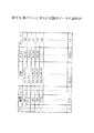
図9は、図7のセルTOPに含まれる図形データを示す。各セルは、複数の図形データを含む。
【0009】
図形は、その種類が矩形(REC)の場合、対角点の座標で表され、種類が多角形(POL)の場合、各頂点の座標で表され、種類が配線の場合、両端の座標で表される。
【0010】
【発明が解決しようとする課題】
図7において、セルA内の図形を修正する場合、セルAのデータをセルTOPのファイルから抽出して別ファイルとし、表示画像を見ながら入力装置を操作して、修正すべき図形を選択し修正を行なう。
【0011】
しかし、例えば同一サイズのコンタクトホールパターンを100個を修正する場合、1個ずつ修正しなければならず、1個当たりの修正時間が約10秒である場合、100個修正すると全修正時間は約20分となる。セルTOPからセルAとBの図形データを抽出し、これらを1つの別ファイルとし、セルA及びBに含まれている複数の同一図形を修正する場合についても同様である。
【0012】
本発明の目的は、このような問題点に鑑み、設計された回路のパターンデータをより短時間で修正することが可能なパターンデータ修正方法及び装置を提供することにある。
【0013】
【課題を解決するための手段及びその作用効果】
本発明では、設計された回路のパターンデータを修正するパターンデータ修正方法において、コンピュータにより、
同一図形データを同一グループにすることにより図形データをグループ化し、
選択された図形データを修正した場合、この図形データと同一グループの他の図形データを自動修正する。
【0014】
この方法によれば、グループ化と自動修正とにより、設計された回路のパターンデータをより短時間で修正することができる。
【0015】
本発明の他の目的、構成及び効果は以下の説明から明らかになる。
【0016】
【発明の実施の形態】
以下、図面を参照して本発明の実施形態を説明する。
【0017】
[第1実施形態]
図1は、本発明の第1実施形態のパターンデータ修正装置を示す概略ブロック図である。
【0018】
この装置は、パターン修正プログラムがインストールされたコンピュータであるパターン修正処理装置10に、入力装置11、表示装置12、記憶装置13及び14が接続されたシステムである。
【0019】
記憶装置13には、例えば図7に示すセルTOPの設計データが格納されており、より具体的には図9に示すような図形データが格納されている。
【0020】
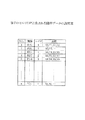
表示装置12の表示を見ながら入力装置11を操作して、セルTOPに含まれている例えばセルA及びBを修正対象として選択する。パターン修正処理装置10はこれに応答して、図4に示す処理を行なう。すなわち、パターン修正処理装置10は、セルA及びBをセルTOPから抽出し、これを別ファイルとして記憶装置14に格納し、記憶装置14に格納されている図9に示す図形データに対し、サイズ及びグループのデータを付加し、図2に示すようなデータを作成する。
【0021】
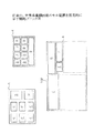
図3(A)、(B)及び(C)はそれぞれ、矩形REC、多角形POL及び配線PTHのサイズを示す。
【0022】
矩形RECのサイズは、横及び縦の長さがW1及びH1である。多角形POLのサイズは、これが内接される矩形の横及び縦の長さW2及びH2である。配線PTHのサイズは、線の長さL1であり、線幅の値はレイヤ毎に統一して与えられている。
【0023】
マスクは、レイヤ毎に製作される。
【0024】
図形の種類、レイヤ及びサイズが同一である場合、同一グループ名を付与する。例えばNO.1とNO.3は図形の種類、レイヤ及びサイズが同一であり、同一グループ名G1が付与されている。
【0025】
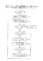
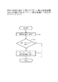
次に、図4のグループ化処理を説明する。
【0026】
(S1)セルA及びBをセルTOPから抽出し、これを別ファイルとして記憶装置14に格納する。
【0027】
(S2)このファイルから、次の図形データを1つ取り出す。最初は、図2中のNO.1の図形データを取り出す。
【0028】
(S3)取り出すべき図形データがなければ処理を終了し、そうでなければステップS4へ進む。
【0029】
(S4)この図形データにグループ名が付与されていればステップS2へ戻り、そうでなければステップS5へ進む。
【0030】
(S5)ステップS2で取り出した図形データにグループ名を付与する。例えば図2中のNO.1の図形に対しグループ名G1を付与する。
【0031】
(S6)この図形データと図形の種類、レイヤ及びサイズが一致する図形データを検索する。
【0032】
(S7)一致する図形データがなければステップS2へ戻り、あればステップS8へ進む。
【0033】
(S8)一致する図形データに対し、ステップS5で付与したグループ名と同一のグループ名を付与する。例えば図2のNO.3の図形データがNO.1のそれに一致する場合、NO.3の図形データにグループ名G1を付与する。
【0034】
ステップS2へ戻り、前回の次の図形データ、例えばNO.2の図形データを取り出す。
【0035】
このようなグループ化処理が終了した後、図5に示す修正処理がパターン修正処理装置10により行なわれる。
【0036】
(S10)操作者は、表示装置12の表示を見ながら入力装置11を操作して、修正対象の図形を選択し修正する。
【0037】
(S11)ステップS10で修正した図形と同一グループ名の図形が図2中に存在すればステップS12へ進み、そうでなければこの選択図形に対する修正処理を終了する。
【0038】
(S12)同一グループの図形をステップS10と同様に修正する。この修正はパターン修正処理装置10により自動的に行われる。
【0039】
例えばステップS10で一辺が1μmの矩形コンタクトホールパターンを一辺が0.9μmの矩形に操作者が修正した場合、これと同一図形がパターン修正処理装置10により自動的に修正される。このような処理により、設計されたパターンデータの修正処理が短時間で行なわれる。例えば100個の同一図形を修正するのに1個あたり約10秒かかり、従来では全体として約20分かかったものが、本実施形態によれば約10秒で全修正が行なわれる。
【0040】
図1において、記憶装置13に格納されているセルTOP内のセルA及びBは、この修正後、記憶装置14内のセルA及びBと置き換えられる。この際、サイズ及びグループのデータが削除される。このサイズ及びグループのデータは記憶装置14に格納され、再度セルA及びBが修正対象として選択された場合にはこのデータが用いられる。
【0041】
なお、本発明には外にも種々の変形例が含まれる。
【0042】
例えば、ポリゴンデータの場合には上記サイズの替わりに、その始点座標が(0,0)となるように図形を平行移動したときの座標値を用いてもよい。また、修正のためにセルTOPから抽出されるセルは1つ以上であればよい。
【図面の簡単な説明】
【図1】本発明の一実施形態のパターンデータ修正装置を示す概略ブロック図である。
【図2】修正対象のセルに含まれる図形データの説明図である。
【図3】(A)、(B)及び(C)はそれぞれ、矩形、多角形及び配線のサイズを説明する図である。
【図4】図1のパターン修正処理装置10により実行されるグループ化処理の手順を示すフローチャートである。
【図5】図4の処理に続いて図1のパターン修正処理装置10により実行されるパターン修正処理の手順を示すフローチャートである。
【図6】従来の、半導体集積回路のセル配置を視覚的に示す概略ブロック図である。
【図7】従来の、セルTOP内にセルA及びBが配置された状態を視覚的に示す図である。
【図8】(A)、(B)及び(C)はそれぞれ、図6中のセルA、B及びTOPの階層構造を示す図である。
【図9】図7のセルTOPに含まれる図形データの説明図である。
【符号の説明】
10 パターン修正処理装置
11 入力装置
12 表示装置
13、14 記憶装置
A〜F、TOP セル[0001]
BACKGROUND OF THE INVENTION
The present invention relates to a pattern data correction method and apparatus for correcting pattern data of a designed circuit.
[0002]
[Prior art]
As the number of functions and pattern density of semiconductor integrated circuits increases, the amount of design data tends to increase, and it is required to correct the designed pattern data in a short time.
[0003]
FIG. 6 is a schematic block diagram visually showing the cell arrangement of the design data of the semiconductor integrated circuit.
[0004]
For example, a semiconductor integrated circuit maker designs cells C to F among the cells TOP of the entire chip, requests an external company to design cell A, and requests another company to design cell B. Cells A and B are placed in cell TOP. In general, the CAD data formats of the designed cells TOP, A and B are different from each other. When the cells A and B are arranged in the cell TOP, these formats are converted into a unified format, for example, the GDS2 format. The cell names in the cells TOP, A, and B are independently assigned. For example, the cell C in the cell TOP and the cell C in the cell A have different contents even if the cell names are the same.
[0005]
FIGS. 8A, 8B, and 8C show the hierarchical structures of cells A, B, and TOP in FIG. 6, respectively. Actually, these hierarchical structures are complicated, but a simple one is shown for explanation.
[0006]
When the cells A and B are arranged in the cell TOP, since the formats are generally different from each other, the cells A and B are expanded and the hierarchical structure is lost.
[0007]
FIG. 7 visually shows a state in which cells A and B are arranged in the cell TOP.
[0008]
FIG. 9 shows graphic data included in the cell TOP of FIG. Each cell includes a plurality of graphic data.
[0009]
When the type is a rectangle (REC), the figure is represented by the coordinates of the diagonal points. When the type is a polygon (POL), it is represented by the coordinates of each vertex. expressed.
[0010]
[Problems to be solved by the invention]
In FIG. 7, when modifying the figure in the cell A, the data of the cell A is extracted from the file of the cell TOP to make another file, and the figure to be corrected is selected by operating the input device while viewing the display image. Make corrections.
[0011]
However, for example, in the case of correcting 100 contact hole patterns of the same size, each must be corrected one by one. If the correction time per pattern is about 10 seconds, the total correction time is about 100 20 minutes. The same applies to the case where the graphic data of the cells A and B are extracted from the cell TOP, and these are used as one separate file, and a plurality of identical graphics included in the cells A and B are corrected.
[0012]
In view of such problems, an object of the present invention is to provide a pattern data correction method and apparatus that can correct pattern data of a designed circuit in a shorter time.
[0013]
[Means for solving the problems and their effects]
In the present invention, in a pattern data correction method for correcting pattern data of a designed circuit,
Group graphic data by grouping the same graphic data into the same group,
When the selected graphic data is corrected, other graphic data in the same group as this graphic data is automatically corrected.
[0014]
According to this method, the pattern data of the designed circuit can be corrected in a shorter time by grouping and automatic correction.
[0015]
Other objects, configurations and effects of the present invention will become apparent from the following description.
[0016]
DETAILED DESCRIPTION OF THE INVENTION
Hereinafter, embodiments of the present invention will be described with reference to the drawings.
[0017]
[First Embodiment]
FIG. 1 is a schematic block diagram showing a pattern data correction apparatus according to the first embodiment of the present invention.
[0018]
This apparatus is a system in which an input device 11, a
[0019]
For example, design data of the cell TOP shown in FIG. 7 is stored in the
[0020]
The input device 11 is operated while viewing the display on the
[0021]
3A, 3B, and 3C show the sizes of the rectangle REC, the polygon POL, and the wiring PTH, respectively.
[0022]
As for the size of the rectangle REC, the horizontal and vertical lengths are W1 and H1. The size of the polygon POL is the horizontal and vertical lengths W2 and H2 of the rectangle in which it is inscribed. The size of the wiring PTH is the line length L1, and the value of the line width is given uniformly for each layer.
[0023]
The mask is manufactured for each layer.
[0024]
When the figure type, layer, and size are the same, the same group name is assigned. For example, NO. 1 and NO. 3 has the same figure type, layer and size, and is given the same group name G1.
[0025]
Next, the grouping process of FIG. 4 will be described.
[0026]
(S1) Cells A and B are extracted from the cell TOP and stored in the
[0027]
(S2) One next graphic data is extracted from this file. Initially, NO. 1 graphic data is extracted.
[0028]
(S3) If there is no graphic data to be extracted, the process is terminated; otherwise, the process proceeds to step S4.
[0029]
(S4) If a group name is assigned to this graphic data, the process returns to step S2, and if not, the process proceeds to step S5.
[0030]
(S5) A group name is assigned to the graphic data extracted in step S2. For example, NO. A group name G1 is assigned to one figure.
[0031]
(S6) This graphic data is searched for graphic data whose graphic type, layer and size match.
[0032]
(S7) If there is no matching figure data, the process returns to step S2, and if there is, the process proceeds to step S8.
[0033]
(S8) The same group name as that assigned in step S5 is assigned to the matching graphic data. For example, the NO. 3 is NO. If it matches that of NO.1, NO. The group name G1 is assigned to the
[0034]
Returning to step S2, the previous next graphic data such as NO. 2 graphic data is extracted.
[0035]
After such grouping processing is completed, the correction processing shown in FIG.
[0036]
(S10) The operator operates the input device 11 while viewing the display on the
[0037]
(S11) If a figure having the same group name as the figure corrected in step S10 exists in FIG. 2, the process proceeds to step S12. Otherwise, the correction process for the selected figure is terminated.
[0038]
(S12) The graphic of the same group is corrected in the same manner as in step S10. This correction is automatically performed by the pattern
[0039]
For example, when the operator corrects a rectangular contact hole pattern having a side of 1 μm to a rectangle having a side of 0.9 μm in
[0040]
In FIG. 1, the cells A and B in the cell TOP stored in the
[0041]
Note that the present invention includes various other modifications.
[0042]
For example, in the case of polygon data, instead of the above size, the coordinate value when the figure is translated so that the starting point coordinate is (0, 0) may be used. Further, one or more cells may be extracted from the cell TOP for correction.
[Brief description of the drawings]
FIG. 1 is a schematic block diagram showing a pattern data correction apparatus according to an embodiment of the present invention.
FIG. 2 is an explanatory diagram of graphic data included in a correction target cell.
FIGS. 3A, 3B, and 3C are diagrams illustrating a rectangle, a polygon, and a wiring size, respectively.
4 is a flowchart showing a procedure of grouping processing executed by the pattern
5 is a flowchart showing a procedure of pattern correction processing executed by the pattern
FIG. 6 is a schematic block diagram visually showing a cell arrangement of a conventional semiconductor integrated circuit.
FIG. 7 is a diagram visually showing a state in which cells A and B are arranged in a cell TOP according to the related art.
8A, 8B, and 8C are diagrams showing the hierarchical structures of cells A, B, and TOP in FIG. 6, respectively.
FIG. 9 is an explanatory diagram of graphic data included in the cell TOP of FIG. 7;
[Explanation of symbols]
DESCRIPTION OF
Claims (3)
図形の種類と、製作されるマスクに対応したレイヤと、座標値とを含む図形データについて、該図形が内接する矩形の隣り合う2辺の長さである図形サイズを求め、該図形サイズを該図形データに付加し、
該種類、該レイヤ及び該サイズが同一である該図形データに同一のグループ名を付加するすることにより、該図形データをグループ化し、
選択された図形データを修正した場合、この図形データと同一グループの他の図形データを自動修正する、
ことを特徴とするパターンデータ修正方法。In a pattern data correction method for correcting pattern data of a designed circuit, a computer
For figure data including a figure type, a layer corresponding to the mask to be manufactured, and coordinate values, a figure size that is the length of two adjacent sides of a rectangle inscribed by the figure is obtained, and the figure size is calculated as the figure size. Add to the graphic data,
The graphic data is grouped by adding the same group name to the graphic data having the same type, layer and size.
When the selected graphic data is corrected, other graphic data in the same group as this graphic data is automatically corrected.
A pattern data correction method characterized by the above.
図形の種類と、製作されるマスクに対応したレイヤと、座標値とを含む図形データについて、該図形が内接する矩形の隣り合う2辺の長さである図形サイズを求め、該図形サイズを該図形データに付加し、
該種類、該レイヤ及び該サイズが同一である該図形データに同一のグループ名を付加するすることにより、該図形データをグループ化し、
選択された図形データを修正した場合、この図形データと同一グループの他の図形データを自動修正する、
コンピュータを有することを特徴とするパターンデータ修正装置。In a pattern data correction device for correcting pattern data of a designed circuit,
For figure data including a figure type, a layer corresponding to the mask to be manufactured, and coordinate values, a figure size that is the length of two adjacent sides of a rectangle inscribed by the figure is obtained, and the figure size is calculated as the figure size. Add to the graphic data,
The graphic data is grouped by adding the same group name to the graphic data having the same type, layer and size.
When the selected graphic data is corrected, other graphic data in the same group as this graphic data is automatically corrected.
A pattern data correction apparatus comprising a computer.
図形の種類と、製作されるマスクに対応したレイヤと、座標値とを含む図形データについて、該図形が内接する矩形の隣り合う2辺の長さである図形サイズを求めさせ、該図形サイズを該図形データに付加させ、
該種類、該レイヤ及び該サイズが同一である該図形データに同一のグループ名を付加させることにより、該図形データをグループ化させ、
選択された図形データを修正した場合、この図形データと同一グループの他の図形データを自動修正させる、
ためのプログラムが記録されたことを特徴とするコンピュータ読み取り可能な記録媒体。To correct the pattern data of the designed circuit ,
For figure data including the type of figure, the layer corresponding to the mask to be manufactured, and the coordinate value, the figure size which is the length of two adjacent sides of the rectangle inscribed by the figure is obtained, and the figure size is Add it to the graphic data,
The graphic data is grouped by adding the same group name to the graphic data having the same type, layer and size.
When the selected graphic data is corrected, other graphic data in the same group as this graphic data is automatically corrected .
A computer-readable recording medium characterized in that a program for recording is recorded .
Priority Applications (2)
| Application Number | Priority Date | Filing Date | Title |
|---|---|---|---|
| JP2000238152A JP4265722B2 (en) | 2000-08-07 | 2000-08-07 | Pattern data correction method and apparatus |
| US09/771,693 US6523164B2 (en) | 2000-08-07 | 2001-01-30 | Method and apparatus for modifying flattened data of designed circuit pattern |
Applications Claiming Priority (1)
| Application Number | Priority Date | Filing Date | Title |
|---|---|---|---|
| JP2000238152A JP4265722B2 (en) | 2000-08-07 | 2000-08-07 | Pattern data correction method and apparatus |
Publications (2)
| Publication Number | Publication Date |
|---|---|
| JP2002049653A JP2002049653A (en) | 2002-02-15 |
| JP4265722B2 true JP4265722B2 (en) | 2009-05-20 |
Family
ID=18729897
Family Applications (1)
| Application Number | Title | Priority Date | Filing Date |
|---|---|---|---|
| JP2000238152A Expired - Fee Related JP4265722B2 (en) | 2000-08-07 | 2000-08-07 | Pattern data correction method and apparatus |
Country Status (2)
| Country | Link |
|---|---|
| US (1) | US6523164B2 (en) |
| JP (1) | JP4265722B2 (en) |
Families Citing this family (3)
| Publication number | Priority date | Publication date | Assignee | Title |
|---|---|---|---|---|
| JP2015050439A (en) * | 2013-09-04 | 2015-03-16 | 株式会社東芝 | Method for correcting drawing data, drawing method, and method for manufacturing mask or template for lithography |
| JP6389040B2 (en) * | 2014-02-17 | 2018-09-12 | 株式会社Screenホールディングス | GUI apparatus, pattern drawing system, job ticket update method and program for pattern drawing apparatus |
| JP6474655B2 (en) * | 2014-09-30 | 2019-02-27 | エイブリック株式会社 | Reticle transmittance measuring method, projection exposure apparatus, and projection exposure method |
Family Cites Families (14)
| Publication number | Priority date | Publication date | Assignee | Title |
|---|---|---|---|---|
| JPS6063405A (en) * | 1983-09-16 | 1985-04-11 | Fujitsu Ltd | Method and device for pattern examination |
| JPS6083328A (en) * | 1983-10-13 | 1985-05-11 | Fujitsu Ltd | Inspecting method of photo-mask |
| JPS63140373A (en) * | 1986-12-02 | 1988-06-11 | Oki Electric Ind Co Ltd | Sheet metal developing method in cad/cam device |
| JPH0574943A (en) | 1991-09-11 | 1993-03-26 | Mitsubishi Electric Corp | Cad device for designing integrated circuit layout pattern |
| US5533148A (en) * | 1993-09-30 | 1996-07-02 | International Business Machines Corporation | Method for restructuring physical design images into hierarchical data models |
| JPH07191199A (en) * | 1993-12-27 | 1995-07-28 | Fujitsu Ltd | Charged particle beam exposure system and exposure method |
| US5553273A (en) * | 1995-04-17 | 1996-09-03 | International Business Machines Corporation | Vertex minimization in a smart optical proximity correction system |
| US5909376A (en) * | 1995-11-20 | 1999-06-01 | Lsi Logic Corporation | Physical design automation system and process for designing integrated circuit chips using highly parallel sieve optimization with multiple "jiggles" |
| KR100225761B1 (en) * | 1996-06-04 | 1999-10-15 | 윤종용 | Method for designing a reticle mask |
| US6076465A (en) * | 1996-09-20 | 2000-06-20 | Kla-Tencor Corporation | System and method for determining reticle defect printability |
| JP3022381B2 (en) * | 1997-03-14 | 2000-03-21 | 日本電気株式会社 | Integrated circuit pattern data processing method |
| JP3396629B2 (en) * | 1998-07-29 | 2003-04-14 | 松下電器産業株式会社 | Mask pattern correction method |
| US6397373B1 (en) * | 1999-07-12 | 2002-05-28 | Taiwan Semiconductor Manufacturing Company | Efficient design rule check (DRC) review system |
| US6353922B1 (en) * | 1999-08-24 | 2002-03-05 | International Business Machines Corporation | Automatic generation of one dimensional data compaction commands for electron beam lithography |
-
2000
- 2000-08-07 JP JP2000238152A patent/JP4265722B2/en not_active Expired - Fee Related
-
2001
- 2001-01-30 US US09/771,693 patent/US6523164B2/en not_active Expired - Lifetime
Also Published As
| Publication number | Publication date |
|---|---|
| US6523164B2 (en) | 2003-02-18 |
| US20020032899A1 (en) | 2002-03-14 |
| JP2002049653A (en) | 2002-02-15 |
Similar Documents
| Publication | Publication Date | Title |
|---|---|---|
| US5847968A (en) | Printed circuit board CAD device which alternates placing components and routing connectors between them | |
| US6553553B2 (en) | Method of designing layout of semiconductor device | |
| JP4265722B2 (en) | Pattern data correction method and apparatus | |
| JP2008112268A (en) | Timing verification method, timing verification apparatus, and timing verification program | |
| JP2010062475A (en) | Layout pattern generating method, method of manufacturing semiconductor device, program, and layout pattern generating device | |
| JPH10256255A (en) | Pattern generation method for semiconductor integrated circuit device | |
| JP3502311B2 (en) | Integrated circuit layout system, layout method, and recording medium | |
| JP4455148B2 (en) | Cell layout drawing creation apparatus and method, and program | |
| JP4411743B2 (en) | Design data conversion apparatus, pattern design support apparatus, design data conversion method, and circuit board pattern design method. | |
| JP3099782B2 (en) | Automatic correction device, automatic correction method, and recording medium for recording automatic correction program for CAM data | |
| JP2002151594A (en) | Semiconductor integrated circuit design method and semiconductor integrated circuit design support apparatus | |
| JP2646849B2 (en) | Computer-aided design equipment | |
| JP3095307B2 (en) | Automatic electric component placement apparatus and automatic electric component placement method | |
| JP3606144B2 (en) | Printed circuit board design system | |
| JP3394873B2 (en) | Press system for metal mask drilling | |
| JP2690657B2 (en) | Layout pattern generator | |
| JPH09212672A (en) | Graphic data processing method | |
| JP4620241B2 (en) | Semiconductor device design support apparatus and method | |
| JPH0143345B2 (en) | ||
| CN118246425A (en) | Report generation method, device, equipment and storage medium | |
| JP2003296373A (en) | Cad program for disaster prevention facility | |
| JP3133718B2 (en) | Layout method | |
| JP2002218213A (en) | Program for digital image display and storage medium with the same stored | |
| CN117574814A (en) | Layout content rapid analysis method based on site distribution | |
| JP2906830B2 (en) | Printed board CAD system |
Legal Events
| Date | Code | Title | Description |
|---|---|---|---|
| A621 | Written request for application examination |
Free format text: JAPANESE INTERMEDIATE CODE: A621 Effective date: 20060726 |
|
| A711 | Notification of change in applicant |
Free format text: JAPANESE INTERMEDIATE CODE: A712 Effective date: 20080728 |
|
| A977 | Report on retrieval |
Free format text: JAPANESE INTERMEDIATE CODE: A971007 Effective date: 20081003 |
|
| A131 | Notification of reasons for refusal |
Free format text: JAPANESE INTERMEDIATE CODE: A131 Effective date: 20081014 |
|
| A521 | Written amendment |
Free format text: JAPANESE INTERMEDIATE CODE: A523 Effective date: 20081212 |
|
| TRDD | Decision of grant or rejection written | ||
| A01 | Written decision to grant a patent or to grant a registration (utility model) |
Free format text: JAPANESE INTERMEDIATE CODE: A01 Effective date: 20090210 |
|
| A01 | Written decision to grant a patent or to grant a registration (utility model) |
Free format text: JAPANESE INTERMEDIATE CODE: A01 |
|
| A61 | First payment of annual fees (during grant procedure) |
Free format text: JAPANESE INTERMEDIATE CODE: A61 Effective date: 20090210 |
|
| R150 | Certificate of patent or registration of utility model |
Free format text: JAPANESE INTERMEDIATE CODE: R150 |
|
| FPAY | Renewal fee payment (event date is renewal date of database) |
Free format text: PAYMENT UNTIL: 20120227 Year of fee payment: 3 |
|
| FPAY | Renewal fee payment (event date is renewal date of database) |
Free format text: PAYMENT UNTIL: 20120227 Year of fee payment: 3 |
|
| S531 | Written request for registration of change of domicile |
Free format text: JAPANESE INTERMEDIATE CODE: R313531 |
|
| S533 | Written request for registration of change of name |
Free format text: JAPANESE INTERMEDIATE CODE: R313533 |
|
| FPAY | Renewal fee payment (event date is renewal date of database) |
Free format text: PAYMENT UNTIL: 20120227 Year of fee payment: 3 |
|
| R350 | Written notification of registration of transfer |
Free format text: JAPANESE INTERMEDIATE CODE: R350 |
|
| FPAY | Renewal fee payment (event date is renewal date of database) |
Free format text: PAYMENT UNTIL: 20130227 Year of fee payment: 4 |
|
| FPAY | Renewal fee payment (event date is renewal date of database) |
Free format text: PAYMENT UNTIL: 20140227 Year of fee payment: 5 |
|
| S531 | Written request for registration of change of domicile |
Free format text: JAPANESE INTERMEDIATE CODE: R313531 |
|
| R350 | Written notification of registration of transfer |
Free format text: JAPANESE INTERMEDIATE CODE: R350 |
|
| LAPS | Cancellation because of no payment of annual fees |