JP4264837B2 - Synchronous rectification type DC-DC converter - Google Patents
Synchronous rectification type DC-DC converter Download PDFInfo
- Publication number
- JP4264837B2 JP4264837B2 JP2005513596A JP2005513596A JP4264837B2 JP 4264837 B2 JP4264837 B2 JP 4264837B2 JP 2005513596 A JP2005513596 A JP 2005513596A JP 2005513596 A JP2005513596 A JP 2005513596A JP 4264837 B2 JP4264837 B2 JP 4264837B2
- Authority
- JP
- Japan
- Prior art keywords
- voltage
- current
- transformer
- signal
- circuit
- Prior art date
- Legal status (The legal status is an assumption and is not a legal conclusion. Google has not performed a legal analysis and makes no representation as to the accuracy of the status listed.)
- Expired - Fee Related
Links
Images


Classifications
-
- H—ELECTRICITY
- H02—GENERATION; CONVERSION OR DISTRIBUTION OF ELECTRIC POWER
- H02M—APPARATUS FOR CONVERSION BETWEEN AC AND AC, BETWEEN AC AND DC, OR BETWEEN DC AND DC, AND FOR USE WITH MAINS OR SIMILAR POWER SUPPLY SYSTEMS; CONVERSION OF DC OR AC INPUT POWER INTO SURGE OUTPUT POWER; CONTROL OR REGULATION THEREOF
- H02M3/00—Conversion of dc power input into dc power output
- H02M3/22—Conversion of dc power input into dc power output with intermediate conversion into ac
- H02M3/24—Conversion of dc power input into dc power output with intermediate conversion into ac by static converters
- H02M3/28—Conversion of dc power input into dc power output with intermediate conversion into ac by static converters using discharge tubes with control electrode or semiconductor devices with control electrode to produce the intermediate ac
- H02M3/325—Conversion of dc power input into dc power output with intermediate conversion into ac by static converters using discharge tubes with control electrode or semiconductor devices with control electrode to produce the intermediate ac using devices of a triode or a transistor type requiring continuous application of a control signal
- H02M3/335—Conversion of dc power input into dc power output with intermediate conversion into ac by static converters using discharge tubes with control electrode or semiconductor devices with control electrode to produce the intermediate ac using devices of a triode or a transistor type requiring continuous application of a control signal using semiconductor devices only
- H02M3/33507—Conversion of dc power input into dc power output with intermediate conversion into ac by static converters using discharge tubes with control electrode or semiconductor devices with control electrode to produce the intermediate ac using devices of a triode or a transistor type requiring continuous application of a control signal using semiconductor devices only with automatic control of the output voltage or current, e.g. flyback converters
-
- H—ELECTRICITY
- H02—GENERATION; CONVERSION OR DISTRIBUTION OF ELECTRIC POWER
- H02M—APPARATUS FOR CONVERSION BETWEEN AC AND AC, BETWEEN AC AND DC, OR BETWEEN DC AND DC, AND FOR USE WITH MAINS OR SIMILAR POWER SUPPLY SYSTEMS; CONVERSION OF DC OR AC INPUT POWER INTO SURGE OUTPUT POWER; CONTROL OR REGULATION THEREOF
- H02M3/00—Conversion of dc power input into dc power output
- H02M3/22—Conversion of dc power input into dc power output with intermediate conversion into ac
- H02M3/24—Conversion of dc power input into dc power output with intermediate conversion into ac by static converters
- H02M3/28—Conversion of dc power input into dc power output with intermediate conversion into ac by static converters using discharge tubes with control electrode or semiconductor devices with control electrode to produce the intermediate ac
- H02M3/325—Conversion of dc power input into dc power output with intermediate conversion into ac by static converters using discharge tubes with control electrode or semiconductor devices with control electrode to produce the intermediate ac using devices of a triode or a transistor type requiring continuous application of a control signal
- H02M3/335—Conversion of dc power input into dc power output with intermediate conversion into ac by static converters using discharge tubes with control electrode or semiconductor devices with control electrode to produce the intermediate ac using devices of a triode or a transistor type requiring continuous application of a control signal using semiconductor devices only
- H02M3/33569—Conversion of dc power input into dc power output with intermediate conversion into ac by static converters using discharge tubes with control electrode or semiconductor devices with control electrode to produce the intermediate ac using devices of a triode or a transistor type requiring continuous application of a control signal using semiconductor devices only having several active switching elements
- H02M3/33571—Half-bridge at primary side of an isolation transformer
-
- H—ELECTRICITY
- H02—GENERATION; CONVERSION OR DISTRIBUTION OF ELECTRIC POWER
- H02M—APPARATUS FOR CONVERSION BETWEEN AC AND AC, BETWEEN AC AND DC, OR BETWEEN DC AND DC, AND FOR USE WITH MAINS OR SIMILAR POWER SUPPLY SYSTEMS; CONVERSION OF DC OR AC INPUT POWER INTO SURGE OUTPUT POWER; CONTROL OR REGULATION THEREOF
- H02M3/00—Conversion of dc power input into dc power output
- H02M3/22—Conversion of dc power input into dc power output with intermediate conversion into ac
- H02M3/24—Conversion of dc power input into dc power output with intermediate conversion into ac by static converters
- H02M3/28—Conversion of dc power input into dc power output with intermediate conversion into ac by static converters using discharge tubes with control electrode or semiconductor devices with control electrode to produce the intermediate ac
- H02M3/325—Conversion of dc power input into dc power output with intermediate conversion into ac by static converters using discharge tubes with control electrode or semiconductor devices with control electrode to produce the intermediate ac using devices of a triode or a transistor type requiring continuous application of a control signal
- H02M3/335—Conversion of dc power input into dc power output with intermediate conversion into ac by static converters using discharge tubes with control electrode or semiconductor devices with control electrode to produce the intermediate ac using devices of a triode or a transistor type requiring continuous application of a control signal using semiconductor devices only
- H02M3/33569—Conversion of dc power input into dc power output with intermediate conversion into ac by static converters using discharge tubes with control electrode or semiconductor devices with control electrode to produce the intermediate ac using devices of a triode or a transistor type requiring continuous application of a control signal using semiconductor devices only having several active switching elements
- H02M3/33576—Conversion of dc power input into dc power output with intermediate conversion into ac by static converters using discharge tubes with control electrode or semiconductor devices with control electrode to produce the intermediate ac using devices of a triode or a transistor type requiring continuous application of a control signal using semiconductor devices only having several active switching elements having at least one active switching element at the secondary side of an isolation transformer
- H02M3/33592—Conversion of dc power input into dc power output with intermediate conversion into ac by static converters using discharge tubes with control electrode or semiconductor devices with control electrode to produce the intermediate ac using devices of a triode or a transistor type requiring continuous application of a control signal using semiconductor devices only having several active switching elements having at least one active switching element at the secondary side of an isolation transformer having a synchronous rectifier circuit or a synchronous freewheeling circuit at the secondary side of an isolation transformer
-
- H—ELECTRICITY
- H02—GENERATION; CONVERSION OR DISTRIBUTION OF ELECTRIC POWER
- H02M—APPARATUS FOR CONVERSION BETWEEN AC AND AC, BETWEEN AC AND DC, OR BETWEEN DC AND DC, AND FOR USE WITH MAINS OR SIMILAR POWER SUPPLY SYSTEMS; CONVERSION OF DC OR AC INPUT POWER INTO SURGE OUTPUT POWER; CONTROL OR REGULATION THEREOF
- H02M3/00—Conversion of dc power input into dc power output
- H02M3/01—Resonant DC/DC converters
-
- Y—GENERAL TAGGING OF NEW TECHNOLOGICAL DEVELOPMENTS; GENERAL TAGGING OF CROSS-SECTIONAL TECHNOLOGIES SPANNING OVER SEVERAL SECTIONS OF THE IPC; TECHNICAL SUBJECTS COVERED BY FORMER USPC CROSS-REFERENCE ART COLLECTIONS [XRACs] AND DIGESTS
- Y02—TECHNOLOGIES OR APPLICATIONS FOR MITIGATION OR ADAPTATION AGAINST CLIMATE CHANGE
- Y02B—CLIMATE CHANGE MITIGATION TECHNOLOGIES RELATED TO BUILDINGS, e.g. HOUSING, HOUSE APPLIANCES OR RELATED END-USER APPLICATIONS
- Y02B70/00—Technologies for an efficient end-user side electric power management and consumption
- Y02B70/10—Technologies improving the efficiency by using switched-mode power supplies [SMPS], i.e. efficient power electronics conversion e.g. power factor correction or reduction of losses in power supplies or efficient standby modes
Description
本発明は、2次側回路でのスイッチング損失を低減することにより変換効率を向上する同期整流型DC−DCコンバータに関する。 The present invention relates to a synchronous rectification type DC-DC converter that improves conversion efficiency by reducing switching loss in a secondary side circuit.
直流電源に接続されて1次側回路を構成する少なくとも1つの主スイッチング素子及びトランスの1次巻線と、トランスの1次巻線に電磁的に結合する2次巻線と、2次巻線と負荷との間に接続され2次側回路を構成する少なくとも1つの整流用スイッチング素子とを備え、主スイッチング素子のスイッチング動作に同期して整流用スイッチング素子を駆動することにより2次側回路から負荷に直流出力を供給する同期整流型DC−DCコンバータは、従来から高効率のスイッチング電源装置として知られている。図14に示す従来の同期整流型DC−DCコンバータは、直流電源(1)に対して直列に接続された第1及び第2の主スイッチング素子としての第1及び第2の主MOS−FET(2,3)と、第1及び第2の主MOS−FET(2,3)の接続点と直流電源(1)の負極端子との間に接続されたトランス(4)の1次巻線(4a)と、トランス(4)の1次巻線(4a)と直列に接続された電流共振用コンデンサ(5)と、第1の主MOS−FET(2)のドレイン−ソース間に接続された電圧擬似共振用コンデンサ(6)と、トランス(4)の2次巻線(4b,4c)に接続された第1及び第2の整流用スイッチング素子としての第1及び第2の整流用MOS−FET(7,8)と、第1及び第2の整流用MOS−FET(7,8)のソース−ドレイン間に各々接続された第1及び第2の出力整流ダイオード(9,10)と、トランス(4)の2次巻線(4b,4c)の中間タップと第1及び第2の整流用MOS−FET(7,8)のソースとの間に接続された出力平滑コンデンサ(11)とを備えている。第1及び第2の主MOS−FET(2,3)、トランス(4)の1次巻線(4a)、電流共振用コンデンサ(5)、電圧擬似共振用コンデンサ(6)は、1次側回路を構成し、トランス(4)の2次巻線(4b,4c)、第1及び第2の整流用MOS−FET(7,8)、第1及び第2の出力整流ダイオード(9,10)、出力平滑コンデンサ(11)は、2次側回路を構成する。 At least one main switching element connected to a DC power source and constituting a primary circuit, a primary winding of the transformer, a secondary winding electromagnetically coupled to the primary winding of the transformer, and the secondary winding And at least one rectifying switching element that is connected between the load and the load and that constitutes the secondary circuit, and drives the rectifying switching element in synchronization with the switching operation of the main switching element, thereby A synchronous rectification type DC-DC converter that supplies a direct current output to a load is conventionally known as a highly efficient switching power supply device. The conventional synchronous rectification type DC-DC converter shown in FIG. 14 includes first and second main MOS-FETs (first and second main MOS-FETs) connected in series to a direct-current power source (1). 2, 3) and the primary winding (4) of the transformer (4) connected between the connection point of the first and second main MOS-FETs (2, 3) and the negative terminal of the DC power source (1). 4a), the current resonance capacitor (5) connected in series with the primary winding (4a) of the transformer (4), and the drain-source of the first main MOS-FET (2). Voltage quasi-resonant capacitor (6) and first and second rectifying MOS- as first and second rectifying switching elements connected to secondary windings (4b, 4c) of transformer (4) The FET (7, 8) and the first and second rectifying MOS-FETs (7, 8) The first and second output rectifier diodes (9, 10) connected between the drain and the drain, the intermediate tap of the secondary winding (4b, 4c) of the transformer (4), and the first and second rectifiers And an output smoothing capacitor (11) connected between the sources of the MOS-FETs (7, 8). The first and second main MOS-FETs (2, 3), the primary winding (4a) of the transformer (4), the current resonance capacitor (5), and the voltage pseudo resonance capacitor (6) are on the primary side. The circuit comprises a secondary winding (4b, 4c) of the transformer (4), first and second rectifying MOS-FETs (7, 8), and first and second output rectifying diodes (9, 10). ), The output smoothing capacitor (11) constitutes a secondary circuit.
トランス(4)は、1次巻線(4a)に電磁的に結合する駆動巻線(4d)と、1次巻線(4a)に直列に接続された漏洩インダクタンス(4e)とを有し、漏洩インダクタンス(4e)は電流共振用リアクトルとして作用する。整流ダイオード(12)及び平滑コンデンサ(13)が接続された駆動巻線(4d)は、制御回路(21)の駆動電源端子(VCC)に駆動用の直流電力を供給する。直流電源(1)の正極端子と平滑コンデンサ(13)との間に接続された起動抵抗(14)を介して、装置起動時に直流電源(1)から流れる電流により平滑コンデンサ(13)を充電し、制御回路(21)を起動させる。第1及び第2の主MOS−FET(2,3)の接続点と起動抵抗(14)との間に直列に接続された整流ダイオード(15)及び平滑コンデンサ(16)は、チャージポンプ回路を構成し、制御回路(21)のハイサイド側の電源端子(VB,VS)間に直流電力を供給する。直流出力電圧V0を検出する出力電圧検出回路(17)は、出力平滑コンデンサ(11)の両端に接続され、トランス(4)の2次巻線(4b,4c)の中間タップと出力電圧検出回路(17)との間にフォトカプラ(18)を構成するフォトダイオード(19)が接続される。フォトダイオード(19)の検出出力信号は、フォトカプラ(18)を構成するフォトトランジスタ(20)に付与され、フォトトランジスタ(20)は、制御回路(21)の帰還信号入力端子(VFB)に接続される。The transformer (4) has a drive winding (4d) electromagnetically coupled to the primary winding (4a) and a leakage inductance (4e) connected in series to the primary winding (4a), The leakage inductance (4e) acts as a current resonance reactor. The drive winding (4d) to which the rectifier diode (12) and the smoothing capacitor (13) are connected supplies driving DC power to the drive power supply terminal (V CC ) of the control circuit (21). The smoothing capacitor (13) is charged by the current flowing from the DC power supply (1) when the apparatus is started up via the starting resistor (14) connected between the positive terminal of the DC power supply (1) and the smoothing capacitor (13). Then, the control circuit (21) is activated. The rectifier diode (15) and the smoothing capacitor (16) connected in series between the connection point of the first and second main MOS-FETs (2, 3) and the starting resistor (14) are connected to the charge pump circuit. Configured to supply DC power between the high-side power supply terminals (V B , V S ) of the control circuit (21). Output voltage detection circuit for detecting a DC output voltage V 0 (17) is connected across the output smoothing capacitor (11), the secondary winding (4b, 4c) intermediate tap and the output voltage detection of the transformer (4) A photodiode (19) constituting a photocoupler (18) is connected between the circuit (17). The detection output signal of the photodiode (19) is applied to the phototransistor (20) constituting the photocoupler (18), and the phototransistor (20) is connected to the feedback signal input terminal (V FB ) of the control circuit (21). Connected.
制御回路(21)は、発振器(22)と、発振器(22)の出力を受信するDフリップフロップ(23)と、Dフリップフロップ(23)の一方の出力端子に接続された第1のデッドタイム付加回路(24)と、第1のデッドタイム付加回路(24)の出力を受信するローサイド側バッファ増幅器(25)と、Dフリップフロップ(23)の他方の出力端子に接続された第2のデッドタイム付加回路(26)と、第2のデッドタイム付加回路(26)の出力を受信するレベル変換回路(27)と、レベル変換回路(27)の出力を受信するハイサイド側バッファ増幅器(28)とを備えている。発振器(22)は、フォトカプラ(18)を介して帰還信号入力端子(VFB)に入力される出力電圧検出回路(17)の検出出力信号の電圧レベルに応じて周波数が変化するパルス信号を出力する。Dフリップフロップ(23)は、発振器(22)から出力されるパルス信号からハイサイド側の第2の駆動パルス信号VG2及びその反転信号であるローサイド側の第1の駆動パルス信号VG1を生成する。第1のデッドタイム付加回路(24)は、Dフリップフロップ(23)の一方の出力端子から出力される第1の駆動パルス信号VG1に一定時間のデッドタイムを付加する。ローサイド側バッファ増幅器(25)は、デッドタイムが付加された第1の駆動パルス信号VG1を第1の主MOS−FET(2)のゲートに付与する。第2のデッドタイム付加回路(26)は、Dフリップフロップ(23)の他方の出力端子から出力される第2の駆動パルス信号VG2に一定時間のデッドタイムを付加する。レベル変換回路(27)は、デッドタイムが付加された第2の駆動パルス信号VG2の電圧レベルを変換する。ハイサイド側バッファ増幅器(28)は、レベル変換回路(27)から出力される第2の駆動パルス信号VG2を第2の主MOS−FET(3)のゲートに付与する。これにより、出力電圧検出回路(17)の検出出力信号の電圧レベルに応じて制御回路(21)からPFM(パルス周波数変調)制御された第1及び第2の駆動パルス信号VG1,VG2がそれぞれ第1及び第2の主MOS−FET(2,3)の各ゲートに付与されるので、出力電圧検出回路(17)の検出出力信号の電圧レベルに対応する周波数で第1及び第2の主MOS−FET(2,3)を交互にオン・オフ動作させることができる。The control circuit (21) includes an oscillator (22), a D flip-flop (23) that receives the output of the oscillator (22), and a first dead time connected to one output terminal of the D flip-flop (23). The additional circuit (24), the low-side buffer amplifier (25) that receives the output of the first dead time adding circuit (24), and the second dead terminal connected to the other output terminal of the D flip-flop (23) A time addition circuit (26), a level conversion circuit (27) that receives the output of the second dead time addition circuit (26), and a high-side buffer amplifier (28) that receives the output of the level conversion circuit (27) And. The oscillator (22) generates a pulse signal whose frequency changes according to the voltage level of the detection output signal of the output voltage detection circuit (17) input to the feedback signal input terminal (V FB ) via the photocoupler (18). Output. The D flip-flop (23) generates the second drive pulse signal V G2 on the high side and the first drive pulse signal V G1 on the low side, which is an inverted signal, from the pulse signal output from the oscillator (22). To do. The first dead time adding circuit (24) adds a fixed dead time to the first drive pulse signal V G1 output from one output terminal of the D flip-flop (23). The low side buffer amplifier (25) applies the first drive pulse signal V G1 to which the dead time is added to the gate of the first main MOS-FET (2). The second dead time addition circuit (26) adds a fixed dead time to the second drive pulse signal V G2 output from the other output terminal of the D flip-flop (23). The level conversion circuit (27) converts the voltage level of the second drive pulse signal V G2 to which the dead time is added. The high-side buffer amplifier (28) applies the second drive pulse signal V G2 output from the level conversion circuit (27) to the gate of the second main MOS-FET (3). As a result, the first and second drive pulse signals V G1 and V G2 subjected to PFM (pulse frequency modulation) control from the control circuit (21) according to the voltage level of the detection output signal of the output voltage detection circuit (17). Since it is given to the gates of the first and second main MOS-FETs (2, 3), respectively, the first and second at a frequency corresponding to the voltage level of the detection output signal of the output voltage detection circuit (17). The main MOS-FETs (2, 3) can be alternately turned on and off.
第1の主MOS−FET(2)のゲートは、第1のコンデンサ(29)及び第1のパルストランス(31)を介して第1の整流用MOS−FET(7)のゲートに接続され、第2の主MOS−FET(3)のゲートは、第2のコンデンサ(30)及び第2のパルストランス(34)を介して第2の整流用MOS−FET(8)のゲートに接続される。このため、制御回路(21)から出力される第1の駆動パルス信号VG1は、第1のコンデンサ(29)を介して第1のパルストランス(31)の1次巻線(32)に入力され、2次巻線(33)から第1の駆動パルス信号VG1と同一波形の第1の同期駆動パルス信号VSC1が発生して第1の整流用MOS−FET(7)のゲートに付与される。一方、第2の駆動パルス信号VG2は、第2のコンデンサ(30)を介して第2のパルストランス(34)の1次巻線(35)に入力され、2次巻線(36)から第2の駆動パルス信号VG2と同一波形の第2の同期駆動パルス信号VSC2が発生して第2の整流用MOS−FET(8)のゲートに付与される。これにより、1次側の第1及び第2の主MOS−FET(2,3)のオン・オフ動作に同期して、2次側の第1及び第2の整流用MOS−FET(7,8)がそれぞれオン・オフ駆動され、2次側回路の出力端子間に発生する略一定レベルの直流出力電圧V0が図示しない負荷に供給される。The gate of the first main MOS-FET (2) is connected to the gate of the first rectifying MOS-FET (7) via the first capacitor (29) and the first pulse transformer (31). The gate of the second main MOS-FET (3) is connected to the gate of the second rectifying MOS-FET (8) through the second capacitor (30) and the second pulse transformer (34). . Therefore, the first drive pulse signal V G1 output from the control circuit (21) is input to the primary winding (32) of the first pulse transformer (31) via the first capacitor (29). The first synchronous drive pulse signal V SC1 having the same waveform as the first drive pulse signal V G1 is generated from the secondary winding (33) and applied to the gate of the first rectifying MOS-FET (7). Is done. On the other hand, the second drive pulse signal V G2 is input to the primary winding (35) of the second pulse transformer (34) via the second capacitor (30), and then from the secondary winding (36). A second synchronous drive pulse signal V SC2 having the same waveform as the second drive pulse signal V G2 is generated and applied to the gate of the second rectifying MOS-FET (8). Thereby, the first and second rectifying MOS-FETs (7, 7) on the secondary side are synchronized with the on / off operation of the first and second main MOS-FETs (2, 3) on the primary side. 8) are respectively turned on and off drive, substantially constant level DC output voltage V 0 which is generated between the output terminals of the secondary circuit is supplied to a load (not shown).
図14に示す同期整流型DC−DCコンバータの動作は以下の通りである。図示しない電源スイッチをオンすると、直流電源(1)から起動抵抗(14)を介して平滑コンデンサ(13)が充電される。平滑コンデンサ(13)の充電電圧が制御回路(21)の起動電圧に達すると、制御回路(21)が動作を開始する。このとき、制御回路(21)から第1及び第2の駆動パルス信号VG1,VG2が出力され、それぞれ第1及び第2の主MOS−FET(2,3)の各ゲートに付与され、第1及び第2の主MOS−FET(2,3)がオン・オフ動作を開始する。第2の主MOS−FET(3)がオン状態のときは、直流電源(1)、第2の主MOS−FET(3)、トランス(4)の漏洩インダクタンス(4e)、1次巻線(4a)、電流共振用コンデンサ(5)及び直流電源(1)の経路で1次側回路に電流IQ2が流れる。電流IQ2は、電流共振用コンデンサ(5)の静電容量及びトランス(4)の漏洩インダクタンス(4e)で決定される共振周波数の共振電流とトランス(4)の1次巻線(4a)の励磁電流との合成電流となる。また、第2の主MOS−FET(3)のオンに同期して第2の整流用MOS−FET(8)がオン状態となり、トランス(4)の2次巻線(4c)から第2の出力整流ダイオード(10)と第2の整流用MOS−FET(8)との並列回路を介して出力平滑コンデンサ(11)及び図示しない負荷に前記の共振電流と略同様の電流IS2が流れる。The operation of the synchronous rectification type DC-DC converter shown in FIG. 14 is as follows. When a power switch (not shown) is turned on, the smoothing capacitor (13) is charged from the DC power supply (1) through the starting resistor (14). When the charging voltage of the smoothing capacitor (13) reaches the starting voltage of the control circuit (21), the control circuit (21) starts its operation. At this time, first and second drive pulse signals V G1 and V G2 are output from the control circuit (21) and applied to the gates of the first and second main MOS-FETs (2, 3), respectively. The first and second main MOS-FETs (2, 3) start an on / off operation. When the second main MOS-FET (3) is in an ON state, the DC power supply (1), the second main MOS-FET (3), the leakage inductance (4e) of the transformer (4), the primary winding ( 4a), the path in the primary circuit of the current resonance capacitor (5) and the DC power source (1) current I Q2 flows. The current I Q2 is the resonance current of the resonance frequency determined by the capacitance of the current resonance capacitor (5) and the leakage inductance (4e) of the transformer (4) and the primary winding (4a) of the transformer (4). This is a combined current with the excitation current. In addition, the second rectifying MOS-FET (8) is turned on in synchronization with the second main MOS-FET (3) being turned on, and the second winding (4c) of the transformer (4) is switched to the second state. Through a parallel circuit of the output rectifier diode (10) and the second rectifying MOS-FET (8), a current I S2 substantially similar to the resonance current flows through the output smoothing capacitor (11) and a load (not shown).
電流IQ2が流れる間に第2の主MOS−FET(3)をオフ状態にすると、第1及び第2の主MOS−FET(2,3)のドレイン−ソース間の電圧VQ1,VQ2は、電圧擬似共振用コンデンサ(6)の静電容量及びトランス(4)の図示しない励磁インダクタンスと漏洩インダクタンス(4e)との合成インダクタンスで決定される共振周波数の擬似共振電圧となる。これと同時に、第2の主MOS−FET(3)に流れるトランス(4)の1次巻線(4a)の励磁電流は、第1の主MOS−FET(2)のドレイン−ソース間の図示しない寄生ダイオードに転流する。寄生ダイオードへの転流期間中に第1の主MOS−FET(2)をオン状態に切り換えると、第1の主MOS−FET(2)の寄生ダイオードに流れる電流はそのまま減少し、極性が反転して第1の主MOS−FET(2)に電流IQ1が流れる。第1の主MOS−FET(2)に流れる電流IQ1は、第2の主MOS−FET(3)に流れる電流IQ2とは逆極性で電流共振用コンデンサ(5)の静電容量及びトランス(4)の漏洩インダクタンス(4e)で決定される共振周波数の共振電流とトランス(4)の1次巻線(4a)の励磁電流との合成電流となる。また、第1の主MOS−FET(2)のオンに同期して第1の整流用MOS−FET(7)がオン状態となり、トランス(4)の2次巻線(4b)から第1の出力整流ダイオード(9)と第1の整流用MOS−FET(7)との並列回路を介して出力平滑コンデンサ(11)及び図示しない負荷に前記の共振電流と略同様の電流IS1が流れる。When the second main MOS-FET (3) is turned off while the current I Q2 flows, the drain-source voltages V Q1 and V Q2 of the first and second main MOS-FETs (2, 3). Is a quasi-resonant voltage having a resonance frequency determined by a capacitance of the voltage quasi-resonance capacitor (6) and a combined inductance of an excitation inductance and a leakage inductance (4e) (not shown) of the transformer (4). At the same time, the exciting current of the primary winding (4a) of the transformer (4) flowing in the second main MOS-FET (3) is illustrated between the drain and source of the first main MOS-FET (2). Does not commutate to parasitic diodes. When the first main MOS-FET (2) is switched on during the commutation period to the parasitic diode, the current flowing through the parasitic diode of the first main MOS-FET (2) is reduced as it is, and the polarity is inverted. Thus, the current IQ1 flows through the first main MOS-FET (2). The current I Q1 flowing through the first main MOS-FET (2) is opposite in polarity to the current I Q2 flowing through the second main MOS-FET (3) and the capacitance and transformer of the current resonance capacitor (5). This is a combined current of the resonance current of the resonance frequency determined by the leakage inductance (4e) of (4) and the excitation current of the primary winding (4a) of the transformer (4). Also, the first rectifying MOS-FET (7) is turned on in synchronization with the first main MOS-FET (2) being turned on, and the first winding from the secondary winding (4b) of the transformer (4) is changed to the first state. output rectifier diode (9) and the first rectifying MOS-FET (7) and the output smoothing capacitor through a parallel circuit (11) and said the not shown load resonance current and substantially the same current I S1 flows.
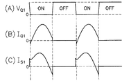
電流IQ1が流れる間に第1の主MOS−FET(2)をオフ状態に切り換えると、第1及び第2の主MOS−FET(2,3)のドレイン−ソース間の電圧VQ1,VQ2は、電圧擬似共振用コンデンサ(6)の静電容量及びトランス(4)の図示しない励磁インダクタンスと漏洩インダクタンス(4e)との合成インダクタンスで決定される共振周波数の擬似共振電圧となる。これと同時に、第1の主MOS−FET(2)に流れるトランス(4)の1次巻線(4a)の励磁電流は、第2の主MOS−FET(3)のドレイン−ソース間の図示しない寄生ダイオードに転流する。寄生ダイオードへの転流期間中に第2の主MOS−FET(3)をオン状態に切り換えると、第2の主MOS−FET(3)の寄生ダイオードに流れる電流はそのまま減少し、極性が反転して第2の主MOS−FET(3)に電流IQ2が流れる。図15(A)、(B)及び(C)は、それぞれ第1の主MOS−FET(2)のドレイン−ソース間の電圧VQ1、第1の主MOS−FET(2)に流れる電流IQ1及びトランス(4)の2次巻線(4b)に流れる電流IS1の各波形を示す。When the first main MOS-FET (2) is switched to the OFF state while the current IQ1 flows, the drain-source voltages VQ1 , V of the first and second main MOS-FETs (2, 3) Q2 is a quasi-resonant voltage having a resonance frequency determined by a capacitance of the voltage quasi-resonance capacitor (6) and a combined inductance of an excitation inductance (not shown) and a leakage inductance (4e) of the transformer (4). At the same time, the exciting current of the primary winding (4a) of the transformer (4) flowing through the first main MOS-FET (2) is illustrated between the drain and source of the second main MOS-FET (3). Does not commutate to parasitic diodes. If the second main MOS-FET (3) is switched on during the commutation period to the parasitic diode, the current flowing through the parasitic diode of the second main MOS-FET (3) is reduced as it is, and the polarity is inverted. Thus, the current IQ2 flows through the second main MOS-FET (3). FIGS. 15A, 15B and 15C show the drain-source voltage V Q1 of the first main MOS-FET (2) and the current I flowing through the first main MOS-FET (2), respectively. Each waveform of the current IS1 flowing through the secondary winding (4b) of Q1 and the transformer (4) is shown.
これ以降は、前記同期整流動作が繰り返され、略一定レベルの直流出力電圧V0が2次側回路から図示しない負荷に印加される。また、第1及び第2の主MOS−FET(2,3)のスイッチング周波数は、トランス(4)の漏洩インダクタンス(4e)と電流共振用コンデンサ(5)の静電容量とで決定される共振周波数より高いため、第1及び第2の主MOS−FET(2,3)のスイッチング周波数を上昇させることにより、図示しない負荷に供給される直流出力を制限できる。前記と略類似の構成を有する同期整流型DC−DCコンバータは、例えば下記の特許文献1に開示されている。
ところで、図14に示す従来の同期整流型DC−DCコンバータでは、トランス(4)の2次側回路の第1及び第2の整流用MOS−FET(7,8)をオン状態にするタイミングを1次側回路の第1及び第2の主MOS−FET(2,3)のターンオンにそれぞれ同期させるため、図15(C)及び(A)に示すように、トランス(4)の2次側回路に流れる電流IS1,IS2は、1次側回路の第1及び第2の主MOS−FET(2,3)のオン期間と一致しない。このため、2次側回路の第1及び第2の出力整流ダイオード(9,10)に電流が流れない期間に第1及び第2の整流用MOS−FET(7,8)がオン状態となるため、出力平滑コンデンサ(11)からトランス(4)の2次巻線(4b,4c)に向かう方向に流れる逆電流が発生する。この逆電流は、更にトランス(4)の1次側と2次側との間を往復する循環電流となり、1次側の第1及び第2の主MOS−FET(2,3)及び2次側の第1及び第2の整流用MOS−FET(7,8)で無用なスイッチング損失を発生するため、同期整流型DC−DCコンバータの変換効率が低下する欠点があった。Incidentally, in the conventional synchronous rectification type DC-DC converter shown in FIG. 14, the timing for turning on the first and second rectification MOS-FETs (7, 8) of the secondary side circuit of the transformer (4) is set. In order to synchronize with the turn-on of the first and second main MOS-FETs (2, 3) of the primary side circuit, respectively, as shown in FIGS. 15C and 15A, the secondary side of the transformer (4) The currents I S1 and I S2 flowing through the circuit do not coincide with the ON periods of the first and second main MOS-FETs (2, 3) of the primary side circuit. Therefore, the first and second rectifying MOS-FETs (7, 8) are turned on during a period in which no current flows through the first and second output rectifying diodes (9, 10) of the secondary side circuit. Therefore, a reverse current that flows in a direction from the output smoothing capacitor (11) toward the secondary windings (4b, 4c) of the transformer (4) is generated. This reverse current further becomes a circulating current that reciprocates between the primary side and the secondary side of the transformer (4), and the primary and second main MOS-FETs (2, 3) and the secondary side of the primary side. Since unnecessary switching losses occur in the first and second rectifying MOS-FETs (7, 8) on the side, there is a drawback that the conversion efficiency of the synchronous rectification type DC-DC converter is lowered.
そこで、本発明は、2次側回路でのスイッチング損失を低減して変換効率を向上できる同期整流型DC−DCコンバータを提供することを目的とする。 Accordingly, an object of the present invention is to provide a synchronous rectification type DC-DC converter that can reduce switching loss in a secondary side circuit and improve conversion efficiency.
本発明による同期整流型DC−DCコンバータは、直流電源(1)に接続されて1次側回路を構成する少なくとも1つの主スイッチング素子(2,3)及びトランス(4)の1次巻線(4a)と、トランス(4)の1次巻線(4a)に電磁的に結合する2次巻線(4b,4c)と負荷との間に接続され2次側回路を構成する少なくとも1つの整流用スイッチング素子(7,8)と、1次側回路に流れる電流(IQ1,IQ2)を検出する電流検出手段(51)と、バイアス電圧(VBS1,VBS2)を発生するバイアス手段(53,54)と、トランス(4)の励磁電流に対応する電圧に比例する傾斜信号(VRP)を発生する傾斜信号発生手段と、電流検出手段(51)の検出電圧(VDT)がバイアス手段(53,54)のバイアス電圧(VBS1,VBS2)と傾斜電圧発生手段の傾斜信号(VRP)との重畳信号の電圧を超えたとき、整流用スイッチング素子(7,8)を駆動する比較手段(55,57)とを備え、主スイッチング素子(2,3)のスイッチング動作に同期して整流用スイッチング素子(7,8)を駆動することにより2次側回路から負荷に直流出力(VO)を供給する。 The synchronous rectification type DC-DC converter according to the present invention includes at least one main switching element (2, 3) and a primary winding of a transformer (4) which are connected to a direct current power source (1) and constitute a primary circuit. 4a) and at least one rectifier composing a secondary circuit connected between a load and a secondary winding (4b, 4c) electromagnetically coupled to a primary winding (4a) of a transformer (4) Switching elements (7, 8), current detection means (51) for detecting currents (I Q1 , I Q2 ) flowing in the primary circuit, and bias means (B BS1 , V BS2 ) for generating bias voltages ( 53, 54), the ramp signal generating means for generating the ramp signal (V RP ) proportional to the voltage corresponding to the excitation current of the transformer (4), and the detection voltage (V DT ) of the current detecting means (51) are biased Drives the rectifying switching element (7, 8) when the voltage of the superimposed signal of the bias voltage (V BS1 , V BS2 ) of the means (53, 54) and the ramp signal (V RP ) of the ramp voltage generating means is exceeded You Comparing means (55, 57) and a DC output from the secondary circuit to the load by driving the rectifying switching elements (7, 8) in synchronization with the switching operation of the main switching elements (2, 3) ( V O ).
これにより、2次側回路に流れる整流出力電流(IS1,IS2)に比例して整流用スイッチング素子(7,8)が駆動されるため、無用な循環電流による電力損失が発生しない。このため、2次側回路を構成する整流用スイッチング素子(7,8)で発生する電力損失を最小限に抑制して同期整流型DC−DCコンバータの変換効率を向上することができる。 As a result, the rectifying switching elements (7, 8) are driven in proportion to the rectified output currents (I S1 , I S2 ) flowing in the secondary circuit, so that power loss due to unnecessary circulating current does not occur. For this reason, the power loss which generate | occur | produces in the switching element (7, 8) for rectification which comprises a secondary side circuit can be suppressed to the minimum, and the conversion efficiency of a synchronous rectification type DC-DC converter can be improved.
本発明による他の同期整流型DC−DCコンバータは、1次側回路に流れる電流(IQ1,IQ2)を検出する電流検出手段(51)と、バイアス電圧(VBS1,VBS2)を発生するバイアス手段(53,54)と、トランス(4)の励磁電流に対応する電圧に比例する傾斜信号(VRP)を発生する傾斜信号発生手段と、電流検出手段(51)の検出電圧(VDT)と傾斜電圧発生手段の傾斜信号(VRP)との重畳信号の電圧がバイアス手段(53,54)のバイアス電圧(VBS1,VBS2)を超えたとき、整流用スイッチング素子(7,8)を駆動する比較手段(55,57)とを備える。傾斜信号発生手段の傾斜信号(VRP)の波形がトランス(4)の1次巻線(4a)に流れる励磁電流の波形と略相似になるため、電流検出手段(51)にて検出された1次側回路の電流(IQ1,IQ2)に含まれるトランス(4)の励磁電流成分を相殺することができる。このため、2次側回路に流れる整流出力電流(IS1,IS2)に正確に比例させて整流用スイッチング素子(7,8)を効率よく駆動することができる。 Another synchronous rectification type DC-DC converter according to the present invention generates current detection means (51) for detecting the current (I Q1 , I Q2 ) flowing in the primary side circuit and the bias voltage (V BS1 , V BS2 ). Bias means (53, 54) for generating a slope signal (V RP ) proportional to the voltage corresponding to the excitation current of the transformer (4), and a detection voltage (V DT ) and the ramp signal (V RP ) of the ramp voltage generating means when the voltage of the superimposed signal exceeds the bias voltage (V BS1 , V BS2 ) of the bias means (53, 54), the rectifying switching element (7, Comparing means (55, 57) for driving 8). Since the waveform of the gradient signal (V RP ) of the gradient signal generating means is substantially similar to the waveform of the excitation current flowing in the primary winding (4a) of the transformer (4), it is detected by the current detection means (51). The exciting current component of the transformer (4) included in the current (I Q1 , I Q2 ) of the primary circuit can be canceled out. For this reason, the rectifying switching elements (7, 8) can be efficiently driven in proportion to the rectified output currents (I S1 , I S2 ) flowing in the secondary circuit.
本発明によれば、2次側回路に流れる整流出力電流に比例して整流用スイッチング素子が駆動されるので、無用な循環電流による電力損失が発生せず、2次側回路の整流用スイッチング素子で発生する電力損失を最小限に抑えて同期整流型DC−DCコンバータの変換効率を向上することができる。トランスの励磁電流に対応する電圧に比例する傾斜信号を発生する傾斜信号発生手段を設けるため、電流検出手段にて検出された1次側回路の電流に含まれるトランスの励磁電流成分が傾斜信号により相殺されるので、2次側回路に流れる整流出力電流に正確に比例させて整流用スイッチング素子を効率よく駆動することができる。バイアス手段のバイアス電圧は、トランスの励磁電流成分より小さい範囲を含む任意のバイアス電圧でよいため、バイアス手段のバイアス電圧を低い値に設定できる利点がある。特に、電流共振方式の同期整流型DC−DCコンバータに本発明を適用する場合は、低耐圧でオン抵抗の低い整流用スイッチング素子を使用できるので、安価で且つ変換効率の極めて高い同期整流型DC−DCコンバータの実現が可能となる。 According to the present invention, since the rectifying switching element is driven in proportion to the rectified output current flowing in the secondary side circuit, power loss due to unnecessary circulating current does not occur, and the rectifying switching element of the secondary side circuit Thus, the conversion efficiency of the synchronous rectification type DC-DC converter can be improved by minimizing the power loss generated in the above. Since the slope signal generating means for generating the slope signal proportional to the voltage corresponding to the transformer excitation current is provided, the transformer excitation current component included in the primary circuit current detected by the current detection means is determined by the slope signal. Since it cancels out, the rectifying switching element can be efficiently driven in proportion to the rectified output current flowing through the secondary circuit. Since the bias voltage of the bias means may be an arbitrary bias voltage including a range smaller than the excitation current component of the transformer, there is an advantage that the bias voltage of the bias means can be set to a low value. In particular, when the present invention is applied to a current resonance type synchronous rectification type DC-DC converter, a rectification switching element having a low breakdown voltage and a low on-resistance can be used, so that the synchronous rectification type DC is inexpensive and has a very high conversion efficiency. -Realization of a DC converter becomes possible.
(1)‥直流電源、(2)‥第1の主MOS−FET(第1の主スイッチング素子)、(3)‥第2の主MOS−FET(第2の主スイッチング素子)、(4)‥トランス、(4a)‥1次巻線、(4b,4c)‥2次巻線、(4d)‥駆動巻線、(4e)‥漏洩インダクタンス、(5)‥電流共振用コンデンサ、(6)‥電圧擬似共振用コンデンサ、(7)‥第1の整流用MOS−FET(第1の整流用スイッチング素子)、(8)‥第2の整流用MOS−FET(第2の整流用スイッチング素子)、(9)‥第1の出力整流ダイオード、(10)‥第2の出力整流ダイオード、(11)‥出力平滑コンデンサ、(12)‥整流ダイオード、(13)‥平滑コンデンサ、(14)‥起動抵抗、(15)‥整流ダイオード、(16)‥平滑コンデンサ、(17)‥出力電圧検出回路、(18)‥フォトカプラ、(19)‥フォトダイオード、(20)‥フォトトランジスタ、(21)‥制御回路、(22)‥発振器、(23)‥Dフリップフロップ、(24)‥第1のデッドタイム付加回路、(25)‥ローサイド側バッファ増幅器、(26)‥第2のデッドタイム付加回路、(27)‥レベル変換回路、(28)‥ハイサイド側バッファ増幅器、(29)‥第1のコンデンサ、(30)‥第2のコンデンサ、(31)‥第1のパルストランス、(32)‥1次巻線、(33)‥2次巻線、(34)‥第2のパルストランス、(35)‥1次巻線、(36)‥2次巻線、(37)‥他の電流共振用コンデンサ、(38)‥他の電圧擬似共振用コンデンサ、(39)‥電流共振用リアクトル、(51)‥電流検出用トランス(電流検出手段)、(52)‥電流検出用抵抗、(53)‥第1の直流バイアス電源(バイアス手段)、(54)‥第2の直流バイアス電源(バイアス手段)、(55)‥第1の比較器(第1の比較手段)、(56)‥第1のバッファ増幅器、(57)‥第2の比較器(第2の比較手段)、(58)‥第2のバッファ増幅器、(59)‥バイアス電源、(60)‥オペアンプ(周波数信号発生手段)、(61)‥抵抗、(62)‥積分コンデンサ、(63)‥駆動用電源、(64)‥波形変換回路(波形変換手段)、(65)‥分流用コンデンサ、(66)‥電圧変換用抵抗、(67,68,70)‥抵抗、(69)‥バイアス電源 (1) ... DC power supply, (2) ... first main MOS-FET (first main switching element), (3) ... second main MOS-FET (second main switching element), (4) Transformer, (4a) Primary winding, (4b, 4c) Secondary winding, (4d) Drive winding, (4e) Leakage inductance, (5) Current resonance capacitor, (6) ··· Voltage pseudo-resonance capacitor, (7) · · · First rectifying MOS-FET (first rectifying switching device), (8) · · · Second rectifying MOS-FET (second rectifying switching device) , (9) ... first output rectifier diode, (10) ... second output rectifier diode, (11) ... output smoothing capacitor, (12) ... rectifier diode, (13) ... smoothing capacitor, (14) ... start-up Resistance (15) Rectifier diode (16) Smoothing resistor Densator, (17) Output voltage detection circuit, (18) Photocoupler, (19) Photodiode, (20) Phototransistor, (21) Control circuit, (22) Oscillator, (23) D Flip-flop, (24) ... first dead time addition circuit, (25) ... low side buffer amplifier, (26) ... second dead time addition circuit, (27) ... level conversion circuit, (28) ... high side Side buffer amplifier, (29) ... first capacitor, (30) ... second capacitor, (31) ... first pulse transformer, (32) ... primary winding, (33) ... secondary winding, (34) ... second pulse transformer, (35) ... primary winding, (36) ... secondary winding, (37) ... other current resonance capacitor, (38) ... other voltage pseudo resonance capacitor , (39) ... Rear for current resonance (51) ... current detection transformer (current detection means), (52) ... current detection resistance, (53) ... first DC bias power supply (bias means), (54) ... second DC bias power supply (Bias means), (55)... First comparator (first comparison means), (56)... First buffer amplifier, (57)... Second comparator (second comparison means), ( 58) Second buffer amplifier, (59) Bias power supply, (60) Operational amplifier (frequency signal generating means), (61) Resistor, (62) Integration capacitor, (63) Drive power supply, 64) ... Waveform conversion circuit (waveform conversion means), (65) ... Capacitor for shunting, (66) ... Resistance for voltage conversion, (67, 68, 70) ... Resistance, (69) ... Bias power supply
以下、同期整流型DC−DCコンバータを電流共振方式の同期整流型DC−DCコンバータに適用した本発明による5つの実施の形態を図1〜図12について説明する。図1〜図12では、図14及び図15に示す箇所と実質的に同一の部分には同一の符号を付し、その説明を省略する。 Hereinafter, five embodiments according to the present invention in which a synchronous rectification type DC-DC converter is applied to a current resonance type synchronous rectification type DC-DC converter will be described with reference to FIGS. 1 to 12, parts that are substantially the same as the parts shown in FIGS. 14 and 15 are given the same reference numerals, and descriptions thereof are omitted.
図1に示すように、本発明の第1の実施の形態を示す同期整流型DC−DCコンバータは、トランス(4)の1次側回路に流れる電流IQ1,IQ2を検出する電流検出手段となる電流検出用トランス(CT:Current Transformer)(51)と、電流検出用トランス(51)の検出電流をそれに対応する電圧VDTに変換する電流検出用抵抗(52)と、トランス(4)の励磁電流に対応する電圧よりも大きいバイアス電圧VBS1,VBS2を発生するバイアス手段としての第1及び第2の直流バイアス電源(53,54)と、非反転入力端子(+)に入力される電流検出用抵抗(52)の検出電圧VDTが反転入力端子(−)に入力される第1の直流バイアス電源(53)のバイアス電圧VBS1を超えたときに第1の整流用MOS−FET(7)をオン状態にする第1の同期駆動パルス信号VSC1を出力する第1の比較手段としての第1の比較器(55)と、第1の比較器(55)の第1の同期駆動パルス信号VSC1を第1の整流用MOS−FET(7)のゲートに付与する第1のバッファ増幅器(56)と、反転入力端子(−)に入力される電流検出用抵抗(52)の検出電圧VDTが非反転入力端子(+)に入力される第2の直流バイアス電源(54)のバイアス電圧VBS2を超えたときに第2の整流用MOS−FET(8)をオン状態にする第2の同期駆動パルス信号VSC2を出力する第2の比較手段としての第2の比較器(57)と、第2の比較器(57)の第2の同期駆動パルス信号VSC2を第2の整流用MOS−FET(8)のゲートに付与する第2のバッファ増幅器(58)とを備えている。第1の直流バイアス電源(53)は、陰極端子が接地され且つ陽極端子が第1の比較器(55)の反転入力端子(−)に接続される。第2の直流バイアス電源(54)は、陽極端子が接地され且つ陰極端子が第2の比較器(57)の非反転入力端子(+)に接続される。電流検出用トランス(51)の右端の2つの黒点は、第1及び第2の主MOS−FET(2,3)の接続点とトランス(4)の1次巻線(4a)との間のライン上に接続される図示しない1次巻線及び電流検出用抵抗(52)の両端に接続される2次巻線が互いに同極性であることを示す。その他の構成は、第1及び第2のコンデンサ(29,30)と第1及び第2のパルストランス(31,34)を省略した点を除き、図14に示す従来の同期整流型DC−DCコンバータと略同様である。As shown in FIG. 1, the synchronous rectification type DC-DC converter showing the first embodiment of the present invention is a current detection means for detecting currents I Q1 and I Q2 flowing in the primary side circuit of the transformer (4). A current detection transformer (CT) (51), a current detection resistor (52) for converting a detection current of the current detection transformer (51) into a corresponding voltage VDT , and a transformer (4) The first and second DC bias power sources (53, 54) as bias means for generating bias voltages V BS1 and V BS2 that are larger than the voltage corresponding to the excitation current are input to the non-inverting input terminal (+). When the detection voltage V DT of the current detection resistor (52) exceeds the bias voltage V BS1 of the first DC bias power supply (53) input to the inverting input terminal (−). A first comparator (55) as a first comparison means for outputting a first synchronous drive pulse signal VSC1 for turning on the first rectifying MOS-FET (7), and a first comparison The first synchronous drive pulse signal V SC1 of the capacitor (55) is applied to the gate of the first rectifying MOS-FET (7) and input to the inverting input terminal (−). second rectifying MOS when the detected voltage V DT of the current detection resistor (52) exceeds the bias voltage V BS2 of the non-inverting input terminal (+) a second DC bias power source to be input to the (54) that A second comparator (57) as a second comparison means for outputting a second synchronous drive pulse signal VSC2 for turning on the FET (8), and a second comparator (57) synchronizing the driving pulse signal V SC2 second rectification MOS-FET of And a second buffer amplifier and (58) to be applied to the gate of 8). The first DC bias power source (53) has a cathode terminal grounded and an anode terminal connected to the inverting input terminal (-) of the first comparator (55). The second DC bias power supply (54) has an anode terminal grounded and a cathode terminal connected to the non-inverting input terminal (+) of the second comparator (57). The two black dots at the right end of the current detection transformer (51) are between the connection point of the first and second main MOS-FETs (2, 3) and the primary winding (4a) of the transformer (4). A primary winding (not shown) connected on the line and a secondary winding connected to both ends of the current detection resistor (52) are shown to have the same polarity. Other configurations are the same as the conventional synchronous rectification type DC-DC shown in FIG. 14 except that the first and second capacitors (29, 30) and the first and second pulse transformers (31, 34) are omitted. It is almost the same as the converter.
上記の構成において、第2の主MOS−FET(3)がオン状態のときは、直流電源(1)、第2の主MOS−FET(3)、トランス(4)の漏洩インダクタンス(4e)、1次巻線(4a)、電流共振用コンデンサ(5)及び直流電源(1)の経路で1次側回路に電流IQ2が流れる。このときの電流IQ2は、電流共振用コンデンサ(5)の静電容量及びトランス(4)の漏洩インダクタンス(4e)で決定される共振周波数の共振電流とトランス(4)の1次巻線(4a)の励磁電流との合成電流となる。1次側回路に流れる電流IQ2は電流検出用トランス(51)にて検出され、更に電流検出用抵抗(52)によりその検出電流に対応する電圧VDTに変換される。即ち、電流検出用抵抗(52)の両端には、図2(A)に示すように接地(グランド)電圧0Vを基準電位として電流検出用トランス(51)の検出電流に比例して変化する電圧VDTが発生する。電流検出用抵抗(52)の検出電圧VDTは第2の比較器(57)の反転入力端子(−)に入力され、非反転入力端子(+)に入力される第2の直流バイアス電源(54)のバイアス電圧VBS2と比較される。図2(A)に示すように、電流検出用抵抗(52)の検出電圧VDTが第2の直流バイアス電源(54)のバイアス電圧VBS2より低くなると、図2(B)に示すように、第2の比較器(57)から第2のバッファ増幅器(58)を介して第2の整流用MOS−FET(8)のゲートに高い電圧(H)レベルの第2の同期駆動パルス信号VSC2が付与され、第2の整流用MOS−FET(8)がオン状態となる。これにより、トランス(4)の2次巻線(4c)から第2の出力整流ダイオード(10)と第2の整流用MOS−FET(8)との並列回路を介して出力平滑コンデンサ(11)及び図示しない負荷に前記の共振電流と略同様の電流IS2が流れる。In the above configuration, when the second main MOS-FET (3) is in the ON state, the DC power supply (1), the second main MOS-FET (3), the leakage inductance (4e) of the transformer (4), A current IQ2 flows through the primary circuit through the path of the primary winding (4a), the current resonance capacitor (5), and the DC power supply (1). The current I Q2 at this time is the resonance current of the resonance frequency determined by the capacitance of the current resonance capacitor (5) and the leakage inductance (4e) of the transformer (4) and the primary winding ( It becomes a combined current with the excitation current of 4a). The current IQ2 flowing through the primary circuit is detected by the current detection transformer (51), and further converted into a voltage VDT corresponding to the detected current by the current detection resistor (52). That is, as shown in FIG. 2A, a voltage that changes in proportion to the detection current of the current detection transformer (51) with the ground (ground) voltage of 0 V as a reference potential as shown in FIG. VDT occurs. The detection voltage V DT of the current detection resistor (52) is input to the inverting input terminal (−) of the second comparator (57) and is input to the non-inverting input terminal (+). 54) of the bias voltage VBS2 . As shown in FIG. 2A, when the detection voltage V DT of the current detection resistor (52) becomes lower than the bias voltage V BS2 of the second DC bias power supply (54), as shown in FIG. The second synchronous drive pulse signal V having a high voltage (H) level is supplied from the second comparator (57) to the gate of the second rectifying MOS-FET (8) through the second buffer amplifier (58). SC2 is applied, and the second rectifying MOS-FET (8) is turned on. As a result, the output smoothing capacitor (11) from the secondary winding (4c) of the transformer (4) through the parallel circuit of the second output rectifier diode (10) and the second rectifier MOS-FET (8). In addition, a current I S2 substantially the same as the resonance current flows through a load (not shown).
電流IQ2が流れる間に第2の主MOS−FET(3)をオフ状態にすると、第1及び第2の主MOS−FET(2,3)のドレイン−ソース間の電圧VQ1,VQ2は、電圧擬似共振用コンデンサ(6)の静電容量及びトランス(4)の図示しない励磁インダクタンスと漏洩インダクタンス(4e)との合成インダクタンスで決定される共振周波数の擬似共振電圧となる。これと同時に、第2の主MOS−FET(3)に流れるトランス(4)の1次巻線(4a)の励磁電流は、第1の主MOS−FET(2)のドレイン−ソース間の図示しない寄生ダイオードに転流する。この転流期間中に第1の主MOS−FET(2)をオン状態にすると、第1の主MOS−FET(2)の寄生ダイオードに流れる電流は、そのまま減少し、極性が反転して第1の主MOS−FET(2)に電流IQ1が流れる。このとき、1次側回路に流れる電流IQ1は、第2の主MOS−FET(3)に流れる電流IQ2とは逆極性で電流共振用コンデンサ(5)の静電容量及びトランス(4)の漏洩インダクタンス(4e)で決定される共振周波数の共振電流とトランス(4)の1次巻線(4a)の励磁電流との合成電流となる。1次側回路に流れる電流IQ1は電流検出用トランス(51)にて検出され、更に電流検出用抵抗(52)によりその検出電流に対応する電圧VDTに変換される。即ち、電流検出用抵抗(52)の両端には、図2(A)に示すように接地(グランド)電圧0Vを基準電位として電流検出用トランス(51)の検出電流に比例して変化する電圧VDTが発生する。電流検出用抵抗(52)の検出電圧VDTは、第1の比較器(55)の非反転入力端子(+)に入力され、反転入力端子(−)に入力される第1の直流バイアス電源(53)のバイアス電圧VBS1と比較される。図2(A)に示すように、電流検出用抵抗(52)の検出電圧VDTが第1の直流バイアス電源(53)のバイアス電圧VBS1より高くなると、図2(C)に示すように、第1の比較器(55)から第1のバッファ増幅器(56)を介して第1の整流用MOS−FET(7)のゲートに高い電圧(H)レベルの第1の同期駆動パルス信号VSC1が付与され、第1の整流用MOS−FET(7)がオン状態となる。これにより、トランス(4)の2次巻線(4b)から第1の出力整流ダイオード(9)と第1の整流用MOS−FET(7)との並列回路を介して出力平滑コンデンサ(11)及び図示しない負荷に前記の共振電流と略同様の電流IS1が流れる。When the second main MOS-FET (3) is turned off while the current I Q2 flows, the drain-source voltages V Q1 and V Q2 of the first and second main MOS-FETs (2, 3). Is a quasi-resonant voltage having a resonance frequency determined by a capacitance of the voltage quasi-resonance capacitor (6) and a combined inductance of an excitation inductance and a leakage inductance (4e) (not shown) of the transformer (4). At the same time, the exciting current of the primary winding (4a) of the transformer (4) flowing in the second main MOS-FET (3) is illustrated between the drain and source of the first main MOS-FET (2). Does not commutate to parasitic diodes. When the first main MOS-FET (2) is turned on during the commutation period, the current flowing through the parasitic diode of the first main MOS-FET (2) is reduced as it is, and the polarity is reversed and the first A current IQ1 flows through one main MOS-FET (2). At this time, the current I Q1 flowing in the primary circuit is opposite in polarity to the current I Q2 flowing in the second main MOS-FET (3) and the capacitance of the current resonance capacitor (5) and the transformer (4) This is a combined current of the resonance current of the resonance frequency determined by the leakage inductance (4e) of the current and the excitation current of the primary winding (4a) of the transformer (4). The current I Q1 flowing through the primary side circuit is detected by the current detection transformer (51), and further converted into a voltage V DT corresponding to the detected current by the current detection resistor (52). That is, as shown in FIG. 2A, a voltage that changes in proportion to the detection current of the current detection transformer (51) with the ground (ground) voltage of 0 V as a reference potential as shown in FIG. VDT occurs. The detection voltage V DT of the current detection resistor (52) is input to the non-inverting input terminal (+) of the first comparator (55) and is input to the inverting input terminal (−). It is compared with the bias voltage VBS1 of (53). As shown in FIG. 2A, when the detection voltage V DT of the current detection resistor (52) becomes higher than the bias voltage V BS1 of the first DC bias power supply (53), as shown in FIG. The first synchronous drive pulse signal V having a high voltage (H) level is supplied from the first comparator (55) to the gate of the first rectifying MOS-FET (7) through the first buffer amplifier (56). SC1 is applied, and the first rectifying MOS-FET (7) is turned on. As a result, the output smoothing capacitor (11) from the secondary winding (4b) of the transformer (4) through the parallel circuit of the first output rectifier diode (9) and the first rectifier MOS-FET (7). In addition, a current I S1 substantially the same as the resonance current flows through a load (not shown).
電流IQ1が流れる間に第1の主MOS−FET(2)をオフ状態にすると、第1及び第2の主MOS−FET(2,3)のドレイン−ソース間の電圧VQ1,VQ2は電圧擬似共振用コンデンサ(6)の静電容量及びトランス(4)の図示しない励磁インダクタンスと漏洩インダクタンス(4e)との合成インダクタンスで決定される共振周波数の擬似共振電圧となる。これと同時に、第1の主MOS−FET(2)に流れるトランス(4)の1次巻線(4a)の励磁電流は、第2の主MOS−FET(3)のドレイン−ソース間の図示しない寄生ダイオードに転流する。この転流期間中に第2の主MOS−FET(3)をオン状態にすると、第2の主MOS−FET(3)の寄生ダイオードに流れる電流はそのまま減少し、極性が反転して第2の主MOS−FET(3)に電流IQ2が流れる。これ以降は、前記同期整流動作が繰り返され、略一定レベルの直流出力電圧V0が2次側回路から図示しない負荷に供給される。図3(A)、(B)及び(C)は、それぞれ第1の主MOS−FET(2)のドレイン−ソース間の電圧VQ1、第1の主MOS−FET(2)に流れる電流IQ1及びトランス(4)の2次巻線(4b)に流れる電流IS1の各波形を示す。When the first main MOS-FET (2) is turned off while the current I Q1 flows, the drain-source voltages V Q1 and V Q2 of the first and second main MOS-FETs (2, 3). Is a quasi-resonant voltage having a resonance frequency determined by a capacitance of the voltage quasi-resonance capacitor (6) and a combined inductance of an excitation inductance (not shown) and a leakage inductance (4e) of the transformer (4). At the same time, the exciting current of the primary winding (4a) of the transformer (4) flowing through the first main MOS-FET (2) is illustrated between the drain and source of the second main MOS-FET (3). Does not commutate to parasitic diodes. When the second main MOS-FET (3) is turned on during the commutation period, the current flowing through the parasitic diode of the second main MOS-FET (3) is reduced as it is, and the polarity is inverted to the second Current IQ2 flows through the main MOS-FET (3). Thereafter, the synchronous rectification operation is repeated, and a substantially constant level DC output voltage V 0 is supplied from the secondary circuit to a load (not shown). 3A, 3B, and 3C show the drain-source voltage V Q1 of the first main MOS-FET (2) and the current I that flows through the first main MOS-FET (2), respectively. Each waveform of the current IS1 flowing through the secondary winding (4b) of Q1 and the transformer (4) is shown.
第1の実施の形態では、トランス(4)の1次側回路に流れる電流IQ1,IQ2を電流検出用トランス(51)により検出し、電流検出用抵抗(52)の検出電圧VDTがトランス(4)の励磁電流に対応する電圧よりも大きい第1及び第2の直流バイアス電源(53,54)のバイアス電圧VBS1,VBS2を超えたとき、第1及び第2の比較器(55,57)から出力される高い電圧(H)レベルの第1及び第2の同期駆動パルス信号VSC1,VSC2により第1及び第2の整流用MOS−FET(7,8)をオン状態にする。これにより、トランス(4)の励磁電流成分を除く1次側回路の電流IQ1,IQ2に同期して第1及び第2の整流用MOS−FET(7,8)を駆動することができる。このため、2次側回路に流れる整流出力電流IS1,IS2に比例して第1及び第2の整流用MOS−FET(7,8)が駆動されるので、無用な循環電流による電力損失が発生しない。したがって、2次側回路を構成する第1及び第2の整流用MOS−FET(7,8)で発生する電力損失を最小限に抑制して同期整流型DC−DCコンバータの変換効率を向上することができる。また、電流共振方式の同期整流型DC−DCコンバータであるため、2次側回路の第1及び第2の整流用MOS−FET(7,8)に印加される電圧を図示しない負荷に供給される直流出力電圧V0の2倍に制限できる。このため、各整流用MOS−FET(7,8)として低耐圧でオン抵抗の低いMOS−FETを使用できるので、安価で且つ変換効率の極めて高い同期整流型DC−DCコンバータを実現できる。In the first embodiment, the currents I Q1 and I Q2 flowing in the primary circuit of the transformer (4) are detected by the current detection transformer (51), and the detection voltage V DT of the current detection resistor (52) is When the bias voltages V BS1 and V BS2 of the first and second DC bias power supplies (53, 54) that are larger than the voltage corresponding to the excitation current of the transformer (4) are exceeded, the first and second comparators ( 55, 57), the first and second rectifying MOS-FETs (7, 8) are turned on by the first and second synchronous drive pulse signals V SC1 , V SC2 of the high voltage (H) level output from To. Accordingly, the first and second rectifying MOS-FETs (7, 8) can be driven in synchronization with the currents I Q1 and I Q2 of the primary circuit excluding the exciting current component of the transformer (4). . For this reason, since the first and second rectifying MOS-FETs (7, 8) are driven in proportion to the rectified output currents I S1 and I S2 flowing through the secondary circuit, power loss due to unnecessary circulating currents Does not occur. Therefore, the power loss generated in the first and second rectifying MOS-FETs (7, 8) constituting the secondary side circuit is suppressed to the minimum, and the conversion efficiency of the synchronous rectification type DC-DC converter is improved. be able to. In addition, since it is a current resonance type synchronous rectification type DC-DC converter, the voltage applied to the first and second rectification MOS-FETs (7, 8) of the secondary side circuit is supplied to a load (not shown). The DC output voltage V 0 can be limited to twice. Therefore, a MOS-FET having a low breakdown voltage and a low on-resistance can be used as each of the rectifying MOS-FETs (7, 8), so that a synchronous rectification type DC-DC converter that is inexpensive and has extremely high conversion efficiency can be realized.
電流検出用抵抗(52)の検出電圧VDTと第1及び第2の直流バイアス電源(53,54)のバイアス電圧VBS1,VBS2とをそれぞれ第1及び第2の比較器(55,57)により比較する図1に示す同期整流型DC−DCコンバータの代わりに、図4に示すように、第1及び第2の直流バイアス電源(53,54)をそれぞれ電流検出用抵抗(52)と第1及び第2の比較器(55,57)との間に直列に接続し、電流検出用抵抗(52)の検出電圧VDTを第1の直流バイアス電源(53)のバイアス電圧VBS1の分だけ負側にシフトさせると共に、第2の直流バイアス電源(54)のバイアス電圧VBS2の分だけ正側にシフトさせ、それぞれのシフト後の検出電圧VDTを第1及び第2の比較器(55,57)により接地(グランド)電圧0Vと比較してもよい。図1及び図4に示す同期整流型DC−DCコンバータでは、それぞれ正出力及び負出力を発生する電源で第1及び第2の比較器(55,57)を駆動するが、実際には単一の出力を発生する電源で駆動する場合が多いため、図5に示すように第1及び第2の比較器(55,57)の基準電圧入力側に別のバイアス電源(59)を接続し、何れか一方の比較器(55,57)の入力電圧範囲を超えないように基準電位となる接地(グランド)電圧0Vをバイアス電源(59)によりシフトすることが望ましい。図4及び図5に示す何れの場合も、得られる作用及び効果は図1の回路と略同様である。The detection voltage V DT of the current detection resistor (52) and the bias voltages V BS1 , V BS2 of the first and second DC bias power supplies (53, 54) are respectively used as the first and second comparators (55, 57). 1), instead of the synchronous rectification type DC-DC converter shown in FIG. 1, the first and second DC bias power supplies (53, 54) are respectively connected to the current detection resistor (52) as shown in FIG. The detection voltage V DT of the current detection resistor (52) is connected in series between the first and second comparators (55, 57), and the bias voltage V BS1 of the first DC bias power supply (53) is The first and second comparators shift the detection voltage V DT after each shift to the negative side by the amount corresponding to the bias voltage V BS2 of the second DC bias power supply (54). (55, 57) Earth (ground) may be compared with a voltage 0V. In the synchronous rectification type DC-DC converter shown in FIGS. 1 and 4, the first and second comparators (55, 57) are driven by a power source that generates a positive output and a negative output, respectively. Therefore, another bias power source (59) is connected to the reference voltage input side of the first and second comparators (55, 57) as shown in FIG. It is desirable to shift the ground (ground) voltage 0 V as a reference potential by the bias power supply (59) so as not to exceed the input voltage range of either one of the comparators (55, 57). In both cases shown in FIGS. 4 and 5, the obtained functions and effects are substantially the same as those of the circuit of FIG.
第1の実施の形態は変更が可能である。例えば、本発明の第2の実施の形態の同期整流型DC−DCコンバータは、図6に示すように、トランス(4)の2次巻線(4c)に発生する電圧の周波数に同期するパルス信号VPLを出力する周波数信号発生手段を構成するオペアンプ(60)と、オペアンプ(60)の出力パルス信号VPLの半周期毎に傾斜が反転する傾斜信号VRPを出力する積分回路を構成する抵抗(61)及び積分コンデンサ(62)とを図1に示す同期整流型DC−DCコンバータに追加し、抵抗(61)及び積分コンデンサ(62)の接続点を第1の直流バイアス電源(53)の陰極端子と第2の直流バイアス電源(54)の陽極端子との接続点に接続したものである。オペアンプ(60)の非反転入力端子(+)は、トランス(4)の2次巻線(4c)に接続され、同反転入力端子(−)は2次側回路の接地端子に接続される。したがって、図7(B)に示すように、トランス(4)の2次巻線(4c)に発生する電圧の周波数で極性が交番する矩形状のパルス信号VPLがオペアンプ(60)の出力端子から出力され、オペアンプ(60)の出力パルス信号VPLにより抵抗(61)を介して積分コンデンサ(62)が抵抗(61)の抵抗値と積分コンデンサ(62)の静電容量との積で決まる時定数で充電及び放電される。これにより、図7(C)に示すように、トランス(4)の2次巻線(4c)の電圧の周波数に同期する傾斜信号VRPが抵抗(61)及び積分コンデンサ(62)の接続点から出力される。即ち、オペアンプ(60)、抵抗(61)及び積分コンデンサ(62)は、トランス(4)の1次巻線(4a)に流れる励磁電流に対応する電圧に比例する傾斜信号VRPを発生する傾斜信号発生手段を構成する。その他の構成は、図1に示す同期整流型DC−DCコンバータと略同様である。The first embodiment can be changed. For example, the synchronous rectification type DC-DC converter according to the second embodiment of the present invention has a pulse synchronized with the frequency of the voltage generated in the secondary winding (4c) of the transformer (4) as shown in FIG. constituting an operational amplifier (60) constituting the frequency signal generating means for outputting a signal V PL, the integrating circuit inclined every half cycle outputs the gradient signal V RP for inverting the output pulse signal V PL of the operational amplifier (60) A resistor (61) and an integrating capacitor (62) are added to the synchronous rectification type DC-DC converter shown in FIG. 1, and a connection point between the resistor (61) and the integrating capacitor (62) is a first DC bias power source (53). Are connected to a connection point between the cathode terminal of the first DC bias power source and the anode terminal of the second DC bias power source (54). The non-inverting input terminal (+) of the operational amplifier (60) is connected to the secondary winding (4c) of the transformer (4), and the inverting input terminal (−) is connected to the ground terminal of the secondary side circuit. Accordingly, as shown in FIG. 7 (B), the output terminal of the transformer rectangular pulse signal V PL operational amplifier whose polarity alternates at the frequency of the voltage generated in the secondary winding (4c) of (4) (60) The integration capacitor (62) is determined by the product of the resistance value of the resistor (61) and the capacitance of the integration capacitor (62) via the resistor (61) by the output pulse signal VPL of the operational amplifier (60). It is charged and discharged with a time constant. As a result, as shown in FIG. 7C, the ramp signal V RP synchronized with the frequency of the voltage of the secondary winding (4c) of the transformer (4) is connected to the connection point between the resistor (61) and the integrating capacitor (62). Is output from. That is, the operational amplifier (60), the resistor (61), and the integrating capacitor (62) generate a gradient signal VRP that is proportional to the voltage corresponding to the excitation current flowing in the primary winding (4a) of the transformer (4). The signal generating means is configured. Other configurations are substantially the same as those of the synchronous rectification type DC-DC converter shown in FIG.
図6に示す回路では、第2の主MOS−FET(3)がオン状態のときに、1次側回路に流れる電流IQ2は、電流検出用トランス(51)にて検出され、電流検出用抵抗(52)によりその検出電流に対応する電圧VDTに変換される。このとき、図7(A)に示すように、接地(グランド)電圧0Vを基準電位として電流検出用トランス(51)の検出電流に比例して変化する電圧VDTが電流検出用抵抗(52)の両端に発生する。電流検出用抵抗(52)の検出電圧VDTは、第2の比較器(57)の反転入力端子(−)に入力され、非反転入力端子(+)に入力される傾斜信号発生手段を構成する抵抗(61)及び積分コンデンサ(62)の接続点に発生する傾斜信号VRPと第2の直流バイアス電源(54)のバイアス電圧VBS2との重畳信号VRP−VBS2の電圧と比較される。即ち、第2の比較器(57)の非反転入力端子(+)には、図7(C)に示す抵抗(61)及び積分コンデンサ(62)の接続点に発生する傾斜信号VRPの電圧を第2の直流バイアス電源(54)のバイアス電圧VBS2の分だけ負側にシフトさせた図7(D)に示す重畳信号VRP−VBS2の電圧が入力される。図7(D)に示すように、電流検出用抵抗(52)の検出電圧VDTが重畳信号VRP−VBS2の電圧より低くなると、図7(E)に示すように、第2の比較器(57)から第2のバッファ増幅器(58)を介して第2の整流用MOS−FET(8)のゲートに高い電圧(H)レベルの第2の同期駆動パルス信号VSC2が付与され、第2の整流用MOS−FET(8)がオン状態となる。In the circuit shown in FIG. 6, when the second main MOS-FET (3) is in the ON state, the current IQ2 flowing through the primary side circuit is detected by the current detection transformer (51), and the current detection transformer The resistor (52) converts the voltage into a voltage VDT corresponding to the detected current. At this time, as shown in FIG. 7A, the voltage V DT that changes in proportion to the detection current of the current detection transformer (51) with the ground (ground) voltage of 0 V as the reference potential is the current detection resistance (52). Occurs at both ends. The detection voltage V DT of the current detection resistor (52) is input to the inverting input terminal (−) of the second comparator (57) and constitutes a ramp signal generating means that is input to the non-inverting input terminal (+). Is compared with the voltage of the superimposed signal V RP −V BS2 of the ramp signal V RP generated at the connection point of the resistor (61) and the integrating capacitor (62) and the bias voltage V BS2 of the second DC bias power source (54). The That is, the voltage of the ramp signal VRP generated at the connection point of the resistor (61) and the integrating capacitor (62) shown in FIG. 7C is applied to the non-inverting input terminal (+) of the second comparator (57). Is input to the voltage of the superimposed signal V RP -V BS2 shown in FIG. 7D, which is shifted to the negative side by the bias voltage V BS2 of the second DC bias power supply (54). As shown in FIG. 7D, when the detection voltage V DT of the
一方、第1の主MOS−FET(2)がオン状態のときに、1次側回路に流れる電流IQ1は電流検出用トランス(51)にて検出され、電流検出用抵抗(52)によりその検出電流に対応する電圧VDTに変換される。このとき、図7(A)に示すように、接地(グランド)電圧0Vを基準電位として電流検出用トランス(51)の検出電流に比例して変化する電圧VDTが電流検出用抵抗(52)の両端に発生する。電流検出用抵抗(52)の検出電圧VDTは、第1の比較器(55)の非反転入力端子(+)に入力され、反転入力端子(−)に入力される傾斜信号発生手段を構成する抵抗(61)及び積分コンデンサ(62)の接続点に発生する傾斜信号VRPの電圧と第1の直流バイアス電源(53)のバイアス電圧VBS1との重畳信号VRP+VBS1の電圧と比較される。即ち、第1の比較器(55)の反転入力端子(−)には、図7(C)に示す抵抗(61)及び積分コンデンサ(62)の接続点に発生する傾斜信号VRPの電圧を第1の直流バイアス電源(53)のバイアス電圧VBS1の分だけ正側にシフトさせた図7(D)に示す重畳信号VRP+VBS1の電圧が入力される。図7(D)に示すように電流検出用抵抗(52)の検出電圧VDTが前記の重畳信号VRP+VBS1の電圧より高くなると、図7(F)に示すように、第1の比較器(55)から第1のバッファ増幅器(56)を介して第1の整流用MOS−FET(7)のゲートに高い電圧(H)レベルの第1の同期駆動パルス信号VSC1が付与され、第1の整流用MOS−FET(7)がオン状態となる。図1に示す同期整流型DC−DCコンバータの動作と略同様である上記の動作を除く図6に示す同期整流型DC−DCコンバータの主回路の基本的な動作の詳細な説明を省略する。On the other hand, when the first main MOS-FET (2) is in the ON state, the current IQ1 flowing in the primary side circuit is detected by the current detection transformer (51) and is detected by the current detection resistor (52). It is converted into a voltage VDT corresponding to the detected current. At this time, as shown in FIG. 7A, the voltage V DT that changes in proportion to the detection current of the current detection transformer (51) with the ground (ground) voltage of 0 V as the reference potential is the current detection resistance (52). Occurs at both ends. The detection voltage V DT of the current detection resistor (52) is input to the non-inverting input terminal (+) of the first comparator (55) and constitutes a ramp signal generating means that is input to the inverting input terminal (−). Compared with the voltage of the superimposed signal V RP + V BS1 between the voltage of the ramp signal V RP generated at the connection point of the resistor (61) and the integrating capacitor (62) and the bias voltage V BS1 of the first DC bias power source (53) Is done. That is, the voltage of the ramp signal VRP generated at the connection point of the resistor (61) and the integrating capacitor (62) shown in FIG. 7C is applied to the inverting input terminal (−) of the first comparator (55). The voltage of the superimposed signal V RP + V BS1 shown in FIG. 7D, which is shifted to the positive side by the bias voltage V BS1 of the first DC bias power supply (53), is input. When the detection voltage V DT of the current detection resistor (52) becomes higher than the voltage of the superimposed signal V RP + V BS1 as shown in FIG. 7 (D), the first comparison is made as shown in FIG. 7 (F). The first synchronous drive pulse signal V SC1 having a high voltage (H) level is applied from the capacitor (55) to the gate of the first rectifying MOS-FET (7) through the first buffer amplifier (56), The first rectifying MOS-FET (7) is turned on. A detailed description of the basic operation of the main circuit of the synchronous rectification type DC-DC converter shown in FIG. 6 excluding the above-described operation that is substantially the same as the operation of the synchronous rectification type DC-DC converter shown in FIG. 1 will be omitted.
第2の実施の形態では、傾斜信号発生手段の積分回路を構成する抵抗(61)及び積分コンデンサ(62)の接続点に発生する傾斜信号VRPの電圧波形がトランス(4)の1次巻線(4a)に流れる励磁電流の波形と略相似になるため、傾斜信号VRPと第1及び第2の直流バイアス電源(53,54)のバイアス電圧VBS1,VBS2との重畳信号で第1及び第2の比較器(55,57)の不感帯を形成することにより、電流検出用トランス(51)にて検出された1次側回路の電流IQ1,IQ2に含まれるトランス(4)の励磁電流成分を相殺することができる。これにより、1次側回路に流れる電流IQ1,IQ2の共振電流成分のみに同期して2次側回路の第1及び第2の整流用MOS−FET(7,8)がオン状態となる。したがって、2次側回路に流れる整流出力電流IS1,IS2に正確に比例させて第1及び第2の整流用MOS−FET(7,8)を効率よく駆動することができる。また、第1及び第2の直流バイアス電源(53,54)のバイアス電圧VBS1,VBS2は、トランス(4)の励磁電流成分より小さい範囲を含む任意のバイアス電圧でよいため、第1の実施の形態に比較して低い値に設定できる利点がある。なお、特に図示はしないが、第2の実施の形態でも図4及び図5に示す第1の実施の形態と略同様の変更が可能である。In the second embodiment, the voltage waveform of the ramp signal VRP generated at the connection point of the resistor (61) and the integrating capacitor (62) constituting the integrating circuit of the ramp signal generating means is the primary winding of the transformer (4). Since the waveform is substantially similar to the waveform of the excitation current flowing through the line (4a), the first signal is a superimposed signal of the ramp signal VRP and the bias voltages V BS1 and V BS2 of the first and second DC bias power supplies (53, 54). By forming dead zones of the first and second comparators (55, 57), the transformer (4) included in the currents I Q1 and I Q2 of the primary circuit detected by the current detection transformer (51) It is possible to cancel the excitation current component of the. Thus, the first and second rectifying MOS-FET of the secondary circuit in synchronism only the resonant current component of the current I Q1, I Q2 flowing through the primary circuit (7, 8) is turned on . Therefore, the first and second rectifying MOS-FETs (7, 8) can be efficiently driven in proportion to the rectified output currents I S1 and I S2 flowing through the secondary circuit. In addition, the bias voltages V BS1 and V BS2 of the first and second DC bias power supplies (53, 54) may be any bias voltage including a range smaller than the excitation current component of the transformer (4). There is an advantage that a low value can be set as compared with the embodiment. Although not particularly illustrated, the second embodiment can be modified in substantially the same manner as the first embodiment shown in FIGS. 4 and 5.
また、本発明の第3の実施の形態を示す同期整流型DC−DCコンバータは、図8に示すように、トランス(4)の2次巻線(4c)に発生する電圧の周波数に同期するパルス信号VPLを出力する周波数信号発生手段を構成するオペアンプ(60)と、オペアンプ(60)の出力パルス信号VPLの半周期毎に傾斜が反転する傾斜信号VRPを出力する積分回路を構成する抵抗(61)及び積分コンデンサ(62)とを図4に示す同期整流型DC−DCコンバータに追加し、抵抗(61)及び積分コンデンサ(62)の接続点を電圧検出用抵抗(52)の基準電位側(図面に向かって左側)に接続したものである。オペアンプ(60)の反転入力端子(−)はトランス(4)の2次巻線(4c)に接続され、同非反転入力端子(+)は2次側回路の接地端子に接続される。したがって、図9(B)に示すように、トランス(4)の2次巻線(4c)に発生する電圧の周波数で極性が交番する矩形状のパルス信号VPLがオペアンプ(60)の出力端子から出力され、オペアンプ(60)の出力パルス信号VPLにより抵抗(61)を介して積分コンデンサ(62)が抵抗(61)の抵抗値と積分コンデンサ(62)の静電容量との積で決まる時定数で充電及び放電される。これにより、図9(C)に示すように、トランス(4)の2次巻線(4c)の電圧の周波数に同期する傾斜信号VRPが抵抗(61)及び積分コンデンサ(62)の接続点から出力される。即ち、オペアンプ(60)、抵抗(61)及び積分コンデンサ(62)は、トランス(4)の1次巻線(4a)に流れる励磁電流に対応する電圧に比例する傾斜信号VRPを発生する傾斜信号発生手段を構成する。その他の構成は、図4に示す同期整流型DC−DCコンバータと略同様である。Moreover, the synchronous rectification type DC-DC converter which shows the 3rd Embodiment of this invention synchronizes with the frequency of the voltage which generate | occur | produces in the secondary winding (4c) of a transformer (4), as shown in FIG. configuration and operational amplifier (60) constituting the frequency signal generating means for outputting a pulse signal V PL, the integrating circuit inclined every half cycle outputs the gradient signal V RP for inverting the output pulse signal V PL of the operational amplifier (60) A resistor (61) and an integrating capacitor (62) are added to the synchronous rectification type DC-DC converter shown in FIG. 4, and the connection point of the resistor (61) and the integrating capacitor (62) is connected to the voltage detecting resistor (52). It is connected to the reference potential side (left side as viewed in the drawing). The inverting input terminal (−) of the operational amplifier (60) is connected to the secondary winding (4c) of the transformer (4), and the non-inverting input terminal (+) is connected to the ground terminal of the secondary side circuit. Accordingly, as shown in FIG. 9 (B), the output terminal of the transformer rectangular pulse signal V PL operational amplifier whose polarity alternates at the frequency of the voltage generated in the secondary winding (4c) of (4) (60) The integration capacitor (62) is determined by the product of the resistance value of the resistor (61) and the capacitance of the integration capacitor (62) via the resistor (61) by the output pulse signal VPL of the operational amplifier (60). It is charged and discharged with a time constant. As a result, as shown in FIG. 9C, the ramp signal V RP synchronized with the frequency of the voltage of the secondary winding (4c) of the transformer (4) is connected to the resistor (61) and the integrating capacitor (62). Is output from. That is, the operational amplifier (60), the resistor (61), and the integrating capacitor (62) generate a gradient signal VRP that is proportional to the voltage corresponding to the excitation current flowing in the primary winding (4a) of the transformer (4). The signal generating means is configured. Other configurations are substantially the same as those of the synchronous rectification type DC-DC converter shown in FIG.
図8に示す第2の主MOS−FET(3)がオン状態のときに、1次側回路に流れる電流IQ2は、電流検出用トランス(51)にて検出され、電流検出用抵抗(52)によりその検出電流に対応する電圧VDTに変換される。このとき、電流検出用抵抗(52)の両端には、傾斜信号発生手段を構成する抵抗(61)及び積分コンデンサ(62)の接続点に発生する傾斜信号VRPの電圧を基準電位として、電流検出用トランス(51)の検出電流に比例して変化する電圧が発生する。即ち、電流検出用抵抗(52)の検出電位側(図面に向かって右側)には、図9(D)に示すように、図9(C)に示す抵抗(61)及び積分コンデンサ(62)の接続点に発生する傾斜信号VRPの電圧と図9(A)に示す電流検出用抵抗(52)の検出電圧VDTとの重畳信号VRP+VDTの電圧が発生する。電流検出用抵抗(52)の検出電位側の重畳電圧VRP+VDTは、第2の直流バイアス電源(54)を介して第2の比較器(57)の反転入力端子(−)に入力され、非反転入力端子(+)に入力される接地(グランド)電圧0Vと比較される。即ち、第2の比較器(57)の反転入力端子(−)には、第2の直流バイアス電源(54)のバイアス電圧VBS2の分だけ重畳電圧VRP+VDTを正側にシフトさせた電圧が入力される。換言すれば、図9(D)に示すように、電流検出用抵抗(52)の検出電位側の重畳電圧VRP+VDTは、第2の比較器(57)により第2の直流バイアス電源(54)のバイアス電圧VBS2と比較される。図9(D)に示すように、重畳電圧VRP+VDTが第2の直流バイアス電源(54)のバイアス電圧VBS2より低くなると、図9(E)に示すように、第2の比較器(57)から第2のバッファ増幅器(58)を介して第2の整流用MOS−FET(8)のゲートに高い電圧(H)レベルの第2の同期駆動パルス信号VSC2が付与され、第2の整流用MOS−FET(8)がオン状態となる。When the second main MOS-FET (3) shown in FIG. 8 is in the on state, the current IQ2 flowing through the primary side circuit is detected by the current detection transformer (51), and the current detection resistor (52 ) To be converted into a voltage VDT corresponding to the detected current. At this time, the current detection resistor (52) is connected to both ends of the current with the voltage of the slope signal VRP generated at the connection point of the resistor (61) and the integrating capacitor (62) constituting the slope signal generating means as a reference potential. A voltage that changes in proportion to the detection current of the detection transformer (51) is generated. That is, on the detection potential side (right side in the drawing) of the current detection resistor (52), as shown in FIG. 9 (D), the resistor (61) and the integrating capacitor (62) shown in FIG. 9 (C). A voltage of the superposition signal V RP + V DT is generated between the voltage of the slope signal V RP generated at the connection point of and the detection voltage V DT of the current detection resistor (52) shown in FIG. 9A. The superimposed voltage V RP + V DT on the detection potential side of the current detection resistor (52) is input to the inverting input terminal (−) of the second comparator (57) via the second DC bias power supply (54). , Compared with a ground voltage 0 V input to the non-inverting input terminal (+). That is, the superimposed voltage V RP + V DT is shifted to the positive side by the bias voltage V BS2 of the second DC bias power supply (54) at the inverting input terminal (−) of the second comparator (57). A voltage is input. In other words, as shown in FIG. 9D, the superimposed voltage V RP + V DT on the detection potential side of the current detection resistor (52) is supplied to the second DC bias power supply (57) by the second comparator (57). 54) of the bias voltage VBS2 . As shown in FIG. 9D, when the superimposed voltage V RP + V DT becomes lower than the bias voltage V BS2 of the second DC bias power supply (54), as shown in FIG. 9E , the second comparator The second synchronous drive pulse signal V SC2 at a high voltage (H) level is applied from (57) to the gate of the second rectifying MOS-FET (8) via the second buffer amplifier (58), 2 rectifying MOS-FET (8) is turned on.
一方、第1の主MOS−FET(2)がオン状態のときに1次側回路に流れる電流IQ1は、電流検出用トランス(51)にて検出され、更に電流検出用抵抗(52)によりその検出電流に対応する電圧VDTに変換される。このとき、電流検出用抵抗(52)の両端には、傾斜信号発生手段を構成する抵抗(61)及び積分コンデンサ(62)の接続点に発生する傾斜信号VRPの電圧を基準電位として、電流検出用トランス(51)の検出電流に比例して変化する電圧が発生する。即ち、電流検出用抵抗(52)の検出電位側(図面に向かって右側)には、図9(D)に示すように、図9(C)に示す抵抗(61)及び積分コンデンサ(62)の接続点に発生する傾斜信号VRPの電圧と図9(A)に示す電流検出用抵抗(52)の検出電圧VDTとの重畳信号VRP+VDTの電圧が発生する。電流検出用抵抗(52)の検出電位側の重畳電圧VRP+VDTは、第1の直流バイアス電源(53)を介して第1の比較器(55)の非反転入力端子(+)に入力され、反転入力端子(−)に入力される接地(グランド)電圧0Vと比較される。即ち、第1の比較器(55)の非反転入力端子(+)には、第1の直流バイアス電源(53)のバイアス電圧VBS1の分だけ重畳電圧VRP+VDTを負側にシフトさせた電圧が入力される。換言すれば、図9(D)に示すように、電流検出用抵抗(52)の検出電位側の重畳電圧VRP+VDTは、第1の比較器(55)により第1の直流バイアス電源(53)のバイアス電圧VBS1と比較される。図9(D)に示すように、重畳電圧VRP+VDTが第1の直流バイアス電源(53)のバイアス電圧VBS1より高くなると、図9(F)に示すように、第1の比較器(55)から第1のバッファ増幅器(56)を介して第1の整流用MOS−FET(7)のゲートに高い電圧(H)レベルの第1の同期駆動パルス信号VSC1が付与され、第1の整流用MOS−FET(7)がオン状態となる。図1に示す同期整流型DC−DCコンバータの動作と略同様である上記の動作を除く図8に示す同期整流型DC−DCコンバータの主回路の基本的な動作の詳細な説明を省略する。On the other hand, when the first main MOS-FET (2) is in the ON state, the current IQ1 flowing in the primary side circuit is detected by the current detection transformer (51) and further by the current detection resistor (52). It is converted into a voltage VDT corresponding to the detected current. At this time, the current detection resistor (52) is connected to both ends of the current with the voltage of the slope signal VRP generated at the connection point of the resistor (61) and the integrating capacitor (62) constituting the slope signal generating means as a reference potential. A voltage that changes in proportion to the detection current of the detection transformer (51) is generated. That is, on the detection potential side (right side in the drawing) of the current detection resistor (52), as shown in FIG. 9 (D), the resistor (61) and the integrating capacitor (62) shown in FIG. 9 (C). A voltage of the superposition signal V RP + V DT is generated between the voltage of the slope signal V RP generated at the connection point of and the detection voltage V DT of the current detection resistor (52) shown in FIG. 9A. The superimposed voltage V RP + V DT on the detection potential side of the current detection resistor (52) is input to the non-inverting input terminal (+) of the first comparator (55) via the first DC bias power supply (53). Then, it is compared with the ground (ground) voltage 0 V inputted to the inverting input terminal (−). That is, the superimposed voltage V RP + V DT is shifted to the negative side by the amount corresponding to the bias voltage V BS1 of the first DC bias power supply (53) at the non-inverting input terminal (+) of the first comparator (55). Input voltage. In other words, as shown in FIG. 9D, the superimposed voltage V RP + V DT on the detection potential side of the current detection resistor (52) is supplied to the first DC bias power source (55) by the first comparator (55). 53) of the bias voltage VBS1 . As shown in FIG. 9 (D), when the superimposed voltage V RP + V DT becomes higher than the bias voltage V BS1 of the first DC bias power supply (53), as shown in FIG. 9 (F), the first comparator The first synchronous drive pulse signal V SC1 having a high voltage (H) level is applied from (55) to the gate of the first rectifying MOS-FET (7) via the first buffer amplifier (56), 1 rectifying MOS-FET (7) is turned on. Detailed description of the basic operation of the main circuit of the synchronous rectification type DC-DC converter shown in FIG. 8 excluding the above-described operation that is substantially the same as the operation of the synchronous rectification type DC-DC converter shown in FIG. 1 will be omitted.
第3の実施の形態では、傾斜信号発生手段の積分回路を構成する抵抗(61)及び積分コンデンサ(62)の接続点に発生する傾斜信号VRPの電圧波形がトランス(4)の1次巻線(4a)に流れる励磁電流の波形と略相似になるため、傾斜信号VRPと電流検出用抵抗(52)の検出電圧VDTとの重畳信号VRP+VDTを第1及び第2の直流バイアス電源(53,54)のバイアス電圧VBS1,VBS2と比較することにより、電流検出用トランス(51)にて検出された1次側回路の電流IQ1,IQ2に含まれるトランス(4)の励磁電流成分を相殺することができる。これにより、1次側回路に流れる電流IQ1,IQ2の共振電流成分のみに同期して2次側回路の第1及び第2の整流用MOS−FET(7,8)がオン状態となる。このため、2次側回路に流れる整流出力電流IS1,IS2に正確に比例させて第1及び第2の整流用MOS−FET(7,8)を効率よく駆動することができる。また、第1及び第2の直流バイアス電源(53,54)のバイアス電圧VBS1,VBS2は、トランス(4)の励磁電流成分より小さい範囲を含む任意のバイアス電圧でよいため、第1の実施の形態に比較して低い値に設定できる利点がある。第3の実施の形態でも図5に示す実施の形態と略同様の変更が可能である。即ち、第3の実施の形態において第1及び第2の比較器(55,57)を単一の出力を発生する電源で駆動する場合、図10に示すように、第1及び第2の比較器(55,57)の基準電圧入力側に別のバイアス電源(59)を接続し、何れか一方の比較器(55,57)の入力電圧範囲を超えないように基準電位となる接地(グランド)電圧0Vをバイアス電源(59)によりシフトさせればよい。また、図10では傾斜信号発生手段を構成するオペアンプ(60)が別の駆動用電源(63)により駆動される。特に図示しないが、第1及び第2の直流バイアス電源(53,54)の接続位置を図1に示す実施の形態と同様の位置に変更することも可能である。In the third embodiment, the voltage waveform of the ramp signal VRP generated at the connection point of the resistor (61) and the integrating capacitor (62) constituting the integrating circuit of the ramp signal generating means is the primary winding of the transformer (4). Since the waveform of the excitation current flowing in the line (4a) is substantially similar, the superimposed signal V RP + V DT of the gradient signal V RP and the detection voltage V DT of the current detection resistor (52) is changed to the first and second direct currents. By comparing with the bias voltages V BS1 and V BS2 of the bias power source (53, 54), the transformer (4) included in the currents I Q1 and I Q2 of the primary circuit detected by the current detection transformer (51) ) Can be canceled out. Thus, the first and second rectifying MOS-FET of the secondary circuit in synchronism only the resonant current component of the current I Q1, I Q2 flowing through the primary circuit (7, 8) is turned on . For this reason, the first and second rectifying MOS-FETs (7, 8) can be efficiently driven in proportion to the rectified output currents I S1 and I S2 flowing in the secondary circuit. In addition, the bias voltages V BS1 and V BS2 of the first and second DC bias power supplies (53, 54) may be any bias voltage including a range smaller than the excitation current component of the transformer (4). There is an advantage that a low value can be set as compared with the embodiment. The third embodiment can be modified in substantially the same way as the embodiment shown in FIG. That is, when the first and second comparators (55, 57) are driven by a power source that generates a single output in the third embodiment, the first and second comparisons are performed as shown in FIG. Another bias power source (59) is connected to the reference voltage input side of the comparator (55, 57), and the ground (ground) serving as the reference potential is set so as not to exceed the input voltage range of one of the comparators (55, 57). The voltage 0V may be shifted by the bias power source (59). In FIG. 10, the operational amplifier (60) constituting the tilt signal generating means is driven by another driving power source (63). Although not shown in particular, the connection position of the first and second DC bias power supplies (53, 54) can be changed to the same position as in the embodiment shown in FIG.
また、図11に示す第4の実施の形態による同期整流型DC−DCコンバータは、図8に示すオペアンプ(60)、抵抗(61)及び積分コンデンサ(62)の代わりに、制御回路(21)内の発振器(22)から出力されるパルス信号をそのパルス信号の半周期毎に傾斜が反転する傾斜信号VRPに変換する波形変換手段としての波形変換回路(64)を設けて、その出力端子を電流検出用抵抗(52)の基準電位側に接続し、第1及び第2のバッファ増幅器(56,58)の出力信号VSC1,VSC2を第1及び第2のコンデンサ(29,30)と第1及び第2のパルストランス(31,34)を介して第1及び第2の整流用MOS−FET(7,8)の各ゲートに付与するように変更したものである。また、図11に示す同期整流型DC−DCコンバータでは、単一の出力を発生する電源で第1及び第2の比較器(55,57)を駆動するため、1次側回路の接地端子(GND)と第1及び第2の比較器(55,57)の基準電圧入力側端子との間にバイアス電源(59)を接続する。その他の構成は、図8に示す同期整流型DC−DCコンバータと略同様である。第4の実施の形態では、第1及び第2のパルストランス(31,34)によりトランス(4)の1次側回路と2次側回路が絶縁されるので、1次側及び2次側回路間での相互干渉が発生し難い利点がある。図8に示す同期整流型DC−DCコンバータの動作と略同様である図11に示す同期整流型DC−DCコンバータの動作の詳細な説明を省略する。Further, the synchronous rectification type DC-DC converter according to the fourth embodiment shown in FIG. 11 has a control circuit (21) instead of the operational amplifier (60), the resistor (61) and the integrating capacitor (62) shown in FIG. provided waveform converting circuit of the waveform converting means for tilting the pulse signal output from the oscillator of the inner (22) every half cycle of the pulse signal is converted into a ramp signal V RP for inverting (64), an output terminal Is connected to the reference potential side of the current detection resistor (52), and the output signals V SC1 and V SC2 of the first and second buffer amplifiers (56, 58) are connected to the first and second capacitors (29, 30). And the first and second pulse transformers (31, 34) and the first and second rectifying MOS-FETs (7, 8) are changed to be applied to the gates. Further, in the synchronous rectification type DC-DC converter shown in FIG. 11, since the first and second comparators (55, 57) are driven by a power source that generates a single output, the ground terminal ( GND) and a bias voltage source (59) are connected between the reference voltage input terminals of the first and second comparators (55, 57). Other configurations are substantially the same as those of the synchronous rectification type DC-DC converter shown in FIG. In the fourth embodiment, since the primary side circuit and the secondary side circuit of the transformer (4) are insulated by the first and second pulse transformers (31, 34), the primary side and secondary side circuits There is an advantage that mutual interference does not easily occur. Detailed description of the operation of the synchronous rectification type DC-DC converter shown in FIG. 11 which is substantially the same as the operation of the synchronous rectification type DC-DC converter shown in FIG. 8 will be omitted.
更に、図12に示す第4の実施の形態による同期整流型DC−DCコンバータは、図11に示す電流検出用トランス(51)の代わりに、電流共振用コンデンサ(5)の両端に直列に接続された分流用コンデンサ(65)及び電圧変換用抵抗(66)と、分流用コンデンサ(65)及び電圧変換用抵抗(66)の接続点と第1及び第2の直流バイアス電源(53,54)の接続点との間に接続された抵抗(67)とで電流検出手段を構成し、図11に示す波形変換回路(64)と第1及び第2の直流バイアス電源(53,54)の接続点との間に抵抗(68)を接続し、第1及び第2の直流バイアス電源(53,54)の接続点と1次側回路の接地端子(GND)との間にバイアス電源(69)及び抵抗(70)を直列に接続し、第1及び第2の直流バイアス電源(53,54)の極性を互いに逆にし、第1及び第2の比較器(55,57)の反転入力端子(−)及び非反転入力端子(+)をそれぞれ互いに入れ替えたものである。その他の構成は、図11に示す同期整流型DC−DCコンバータと略同様である。第4の実施の形態では、1次側回路の電流共振用コンデンサ(5)に流れる電流を分流用コンデンサ(65)に僅かに分流することにより検出し、その検出電流を電圧変換用抵抗(66)により電圧に変換し、その検出電圧を抵抗(67)を介して第1及び第2の直流バイアス電源(53,54)に重畳する。このため、図11に示す電流検出用トランス(51)に比較して安価なコンデンサ及び抵抗により電流検出手段を構成できると共に、1次側回路に流れる電流IQ1,IQ2を効率よく低損失で検出できる利点がある。図8に示す同期整流型DC−DCコンバータの動作と略同様である図12に示す同期整流型DC−DCコンバータの動作の詳細な説明を省略する。Furthermore, the synchronous rectification type DC-DC converter according to the fourth embodiment shown in FIG. 12 is connected in series with both ends of the current resonance capacitor (5) instead of the current detection transformer (51) shown in FIG. The shunt capacitor (65) and the voltage converting resistor (66), the connection point of the shunt capacitor (65) and the voltage converting resistor (66), and the first and second DC bias power sources (53, 54). The resistor (67) connected to the connection point of the current constitutes current detection means, and the waveform conversion circuit (64) shown in FIG. 11 and the first and second DC bias power supplies (53, 54) are connected. A resistor (68) is connected between the point and the bias power source (69) between the connection point of the first and second DC bias power sources (53, 54) and the ground terminal (GND) of the primary circuit. And a resistor (70) in series, the first and the first In which the polarities of the DC bias power supplies (53, 54) of the first and second comparators (55, 57) are reversed from each other, and the inverting input terminal (-) and the non-inverting input terminal (+) of the first and second comparators (55, 57) are interchanged. It is. Other configurations are substantially the same as those of the synchronous rectification type DC-DC converter shown in FIG. In the fourth embodiment, the current flowing in the current resonance capacitor (5) of the primary side circuit is detected by being slightly diverted to the shunt capacitor (65), and the detected current is detected by the voltage conversion resistor (66 ), And the detected voltage is superimposed on the first and second DC bias power sources (53, 54) via the resistor (67). For this reason, the current detection means can be configured by a cheap capacitor and resistor as compared with the current detection transformer (51) shown in FIG. 11, and the currents I Q1 and I Q2 flowing through the primary side circuit can be efficiently and low loss. There is an advantage that can be detected. Detailed description of the operation of the synchronous rectification type DC-DC converter shown in FIG. 12, which is substantially the same as the operation of the synchronous rectification type DC-DC converter shown in FIG. 8, will be omitted.
本発明の実施態様は前記5つの実施の形態に限定されず、更に種々の変更が可能である。例えば、図5に示す同期整流型DC−DCコンバータは、図13に示すような変更が可能である。即ち、図13に示す同期整流型DC−DCコンバータでは、トランス(4)の1次巻線(4a)と電流共振用コンデンサ(5)の接続点と第2の主MOS−FET(3)のドレインとの間に他の電流共振用コンデンサ(37)を接続し、第2の主MOS−FET(3)のドレイン−ソース間に他の電圧擬似共振用コンデンサ(38)を接続し、図1に示すトランス(4)の漏洩インダクタンス(4e)を電流共振用リアクトルとして使用する代わりに1次巻線(4a)と直列に外付けの電流共振用リアクトル(39)を接続し、2次側の第1及び第2の整流用MOS−FET(7,8)の取り付け位置を負極側から正極側に変更し、第1及び第2の直流バイアス電源(53,54)の極性を互いに逆にし、第1及び第2の比較器(55,57)の反転入力端子(−)及び非反転入力端子(+)をそれぞれ互いに入れ替えている。図13に示す同期整流型DC−DCコンバータの動作は、2次側回路に流れる整流出力電流IS1,IS2の方向が図5とは逆になるため、第1及び第2の同期駆動パルス信号VSC1,VSC2のオン期間が互いに入れ替わる点、及びドライブ回路のレベルが異なる点を除き、図5に示す同期整流型DC−DCコンバータの動作と略同様となる。したがって、図13に示す同期整流型DC−DCコンバータでは、第1の実施の形態と略同様の作用及び効果が得られる。また、第1の実施の形態の図1、図4及び第2〜第5の実施の形態についても前記と同様の変更が可能である。また、第1〜第5の実施の形態での2次側の第1及び第2の出力整流ダイオード(9,10)の代わりに、第1及び第2の整流用MOS−FET(7,8)のドレイン−ソース間の内蔵ダイオードを使用してもよい。また、第1〜第5の実施の形態では、トランス(4)の1次側回路をハーフブリッジ型とする代わりに、フルブリッジ型、プッシュプル型又はフォワード型とすることもできる。更に、トランス(4)の2次側の整流回路を半波整流型にも変更できる。Embodiments of the present invention are not limited to the five embodiments described above, and various modifications can be made. For example, the synchronous rectification type DC-DC converter shown in FIG. 5 can be modified as shown in FIG. That is, in the synchronous rectification type DC-DC converter shown in FIG. 13, the connection point between the primary winding (4a) of the transformer (4) and the current resonance capacitor (5) and the second main MOS-FET (3). Another current resonance capacitor (37) is connected between the drain and another voltage pseudo resonance capacitor (38) is connected between the drain and source of the second main MOS-FET (3). Instead of using the leakage inductance (4e) of the transformer (4) shown in FIG. 5 as a current resonance reactor, an external current resonance reactor (39) is connected in series with the primary winding (4a), and the secondary side The mounting position of the first and second rectifying MOS-FETs (7, 8) is changed from the negative electrode side to the positive electrode side, and the polarities of the first and second DC bias power supplies (53, 54) are reversed to each other, First and second comparators (55, 57 The inverting input terminal (-) and the non-inverting input terminal (+) are interchanged each other. The operation of the synchronous rectification type DC-DC converter shown in FIG. 13 is such that the directions of the rectified output currents I S1 and I S2 flowing through the secondary side circuit are opposite to those in FIG. Except for the fact that the ON periods of the signals V SC1 and V SC2 are interchanged and the level of the drive circuit is different, the operation is substantially the same as the operation of the synchronous rectification type DC-DC converter shown in FIG. Therefore, the synchronous rectification type DC-DC converter shown in FIG. 13 can obtain substantially the same operations and effects as those of the first embodiment. In addition, the same changes as described above can be made to FIGS. 1 and 4 and the second to fifth embodiments of the first embodiment. Further, instead of the first and second output rectifier diodes (9, 10) on the secondary side in the first to fifth embodiments, the first and second rectifying MOS-FETs (7, 8) are used. ) A built-in diode between the drain and the source may be used. In the first to fifth embodiments, the primary side circuit of the transformer (4) may be a full bridge type, a push-pull type, or a forward type instead of the half bridge type. Furthermore, the secondary side rectifier circuit of the transformer (4) can be changed to a half-wave rectifier type.
本発明は、電流共振方式の同期整流型DC−DCコンバータに効果が顕著である。 The effect of the present invention is remarkable in a current resonance type synchronous rectification type DC-DC converter.
Claims (5)
前記1次側回路に流れる電流を検出する電流検出手段と、バイアス電圧を発生するバイアス手段と、前記トランスの励磁電流に対応する電圧に比例する傾斜信号を発生する傾斜信号発生手段と、前記電流検出手段の検出電圧が前記バイアス手段のバイアス電圧と前記傾斜電圧発生手段の傾斜信号との重畳信号の電圧を超えたとき、前記整流用スイッチング素子を駆動する比較手段とを備えたことを特徴とする同期整流型DC−DCコンバータ。Between at least one main switching element and a primary winding of a transformer connected to a DC power source and constituting a primary side circuit, and a secondary winding electromagnetically coupled to the primary winding of the transformer and a load And at least one rectifying switching element constituting a secondary side circuit, and driving the rectifying switching element in synchronization with the switching operation of the main switching element, thereby enabling the secondary side circuit to In the synchronous rectification type DC-DC converter for supplying a direct current output to the load,
Current detecting means for detecting a current flowing in the primary circuit, bias means for generating a bias voltage, a slope signal generating means for generating a slope signal proportional to a voltage corresponding to the excitation current of the transformer, and the current Comparing means for driving the rectifying switching element when the detection voltage of the detecting means exceeds the voltage of the superimposed signal of the bias voltage of the bias means and the ramp signal of the ramp voltage generating means, Synchronous rectification type DC-DC converter.
前記1次側回路に流れる電流を検出する電流検出手段と、バイアス電圧を発生するバイアス手段と、前記トランスの励磁電流に対応する電圧に比例する傾斜信号を発生する傾斜信号発生手段と、前記電流検出手段の検出電圧と前記傾斜電圧発生手段の傾斜信号との重畳信号の電圧が前記バイアス手段のバイアス電圧を超えたとき、前記整流用スイッチング素子を駆動する比較手段とを備えたことを特徴とする同期整流型DC−DCコンバータ。Between at least one main switching element and a primary winding of a transformer connected to a DC power source and constituting a primary side circuit, and a secondary winding electromagnetically coupled to the primary winding of the transformer and a load And at least one rectifying switching element constituting a secondary side circuit, and driving the rectifying switching element in synchronization with the switching operation of the main switching element, thereby enabling the secondary side circuit to In the synchronous rectification type DC-DC converter for supplying a direct current output to the load,
Current detecting means for detecting a current flowing in the primary circuit, bias means for generating a bias voltage, a slope signal generating means for generating a slope signal proportional to a voltage corresponding to the excitation current of the transformer, and the current Comparing means for driving the rectifying switching element when the voltage of the superimposed signal of the detection voltage of the detecting means and the slope signal of the slope voltage generating means exceeds the bias voltage of the bias means, Synchronous rectification type DC-DC converter.
Applications Claiming Priority (3)
| Application Number | Priority Date | Filing Date | Title |
|---|---|---|---|
| JP2003310350 | 2003-09-02 | ||
| JP2003310350 | 2003-09-02 | ||
| PCT/JP2004/008314 WO2005025043A1 (en) | 2003-09-02 | 2004-06-14 | Synchronous commutation dc-dc converter |
Publications (2)
| Publication Number | Publication Date |
|---|---|
| JPWO2005025043A1 JPWO2005025043A1 (en) | 2007-10-04 |
| JP4264837B2 true JP4264837B2 (en) | 2009-05-20 |
Family
ID=34269644
Family Applications (1)
| Application Number | Title | Priority Date | Filing Date |
|---|---|---|---|
| JP2005513596A Expired - Fee Related JP4264837B2 (en) | 2003-09-02 | 2004-06-14 | Synchronous rectification type DC-DC converter |
Country Status (3)
| Country | Link |
|---|---|
| US (1) | US7330365B2 (en) |
| JP (1) | JP4264837B2 (en) |
| WO (1) | WO2005025043A1 (en) |
Cited By (2)
| Publication number | Priority date | Publication date | Assignee | Title |
|---|---|---|---|---|
| JP2014132806A (en) * | 2013-01-07 | 2014-07-17 | Murata Mfg Co Ltd | Insulation type switching power supply device |
| US9071159B2 (en) | 2009-07-31 | 2015-06-30 | Daikin Industries, Ltd. | Power converter |
Families Citing this family (44)
| Publication number | Priority date | Publication date | Assignee | Title |
|---|---|---|---|---|
| TW200605483A (en) * | 2004-03-31 | 2006-02-01 | Matsushita Electric Ind Co Ltd | Inductive load current control circuit and power supply apparatus |
| TW200740089A (en) * | 2006-03-07 | 2007-10-16 | Rohm Co Ltd | Capacitor charging apparatus |
| JP2007274789A (en) * | 2006-03-30 | 2007-10-18 | Densei Lambda Kk | Switching power supply device |
| EP1860838B1 (en) * | 2006-05-24 | 2013-08-14 | Infineon Technologies AG | Data transmission using phase modulation over two signal paths |
| TW200803136A (en) * | 2006-06-26 | 2008-01-01 | Acbel Polytech Inc | Synchronous voltage modulation circuit for resonant power conversion circuit |
| DE102006033348B4 (en) * | 2006-07-19 | 2011-06-22 | Loewe Opta GmbH, 96317 | resonant converter |
| TWI342679B (en) * | 2007-02-27 | 2011-05-21 | Jmicron Technology Corp | Transceiver circuit capable of separating hybrid signal by current |
| CN101345487B (en) * | 2008-05-21 | 2014-03-12 | 英飞特电子(杭州)股份有限公司 | Primary sampling current controlled synchronous commutation driving circuit |
| JP5397024B2 (en) * | 2008-09-16 | 2014-01-22 | 富士電機株式会社 | Switching power supply device, switching power supply control circuit, and switching power supply device control method |
| JP5092023B2 (en) | 2009-02-06 | 2012-12-05 | 新電元工業株式会社 | Current detection circuit and transformer current measurement system |
| WO2011133542A1 (en) * | 2010-04-19 | 2011-10-27 | Rf Micro Devices, Inc. | Pseudo-envelope following power management system |
| US8456868B2 (en) | 2010-04-30 | 2013-06-04 | Infineon Technologies Ag | Controller for a resonant switched-mode power converter |
| US8665611B2 (en) | 2010-04-30 | 2014-03-04 | Infineon Technologies Ag | Controller for a resonant switched-mode power converter |
| CN101895207A (en) * | 2010-06-28 | 2010-11-24 | 华为技术有限公司 | Control circuit and method and power supply device |
| JP5599663B2 (en) * | 2010-07-07 | 2014-10-01 | 新電元工業株式会社 | Drive signal generation circuit, control device, switching power supply device, and control method |
| CN101895201B (en) * | 2010-07-23 | 2015-06-10 | 中兴通讯股份有限公司 | LLC (Logical Link Control) series resonance converter and drive method thereof |
| US8817494B2 (en) * | 2010-08-09 | 2014-08-26 | Sanken Electric Co., Ltd. | PFC AC/DC converter reducing harmonics, switching loss, and switching noise |
| TW201210184A (en) * | 2010-08-23 | 2012-03-01 | Skynet Electronic Co Ltd | Series resonant converter capable of reducing rated voltage and rated current of power switch |
| US9954436B2 (en) | 2010-09-29 | 2018-04-24 | Qorvo Us, Inc. | Single μC-buckboost converter with multiple regulated supply outputs |
| CN103229403B (en) * | 2010-12-02 | 2015-11-25 | 株式会社村田制作所 | Switching power circuit |
| JP2014529292A (en) * | 2011-10-14 | 2014-10-30 | オークランド ユニサービシズ リミテッドAuckland Uniservices Limited | Passive switch converter and circuit including the same |
| US9484797B2 (en) | 2011-10-26 | 2016-11-01 | Qorvo Us, Inc. | RF switching converter with ripple correction |
| US9515621B2 (en) | 2011-11-30 | 2016-12-06 | Qorvo Us, Inc. | Multimode RF amplifier system |
| US9494962B2 (en) | 2011-12-02 | 2016-11-15 | Rf Micro Devices, Inc. | Phase reconfigurable switching power supply |
| US9813036B2 (en) | 2011-12-16 | 2017-11-07 | Qorvo Us, Inc. | Dynamic loadline power amplifier with baseband linearization |
| US9627975B2 (en) | 2012-11-16 | 2017-04-18 | Qorvo Us, Inc. | Modulated power supply system and method with automatic transition between buck and boost modes |
| US9300252B2 (en) | 2013-01-24 | 2016-03-29 | Rf Micro Devices, Inc. | Communications based adjustments of a parallel amplifier power supply |
| US8964421B2 (en) * | 2013-03-14 | 2015-02-24 | Dialog Semiconductor Inc. | Powering a synchronous rectifier controller |
| CN104113213B (en) * | 2013-04-17 | 2017-12-12 | 比亚迪股份有限公司 | A kind of DC DC converting means for electric automobile |
| JP6148551B2 (en) * | 2013-06-26 | 2017-06-14 | 株式会社東芝 | Rectifier |
| US9356535B2 (en) * | 2013-08-14 | 2016-05-31 | Stmicroelectronics S.R.L. | Control method for rectifier of switching converters |
| US9209703B2 (en) * | 2013-08-14 | 2015-12-08 | Stmicroelectronics S.R.L. | Control device for a rectifier of a switching converter |
| NL2011919C2 (en) * | 2013-12-09 | 2015-06-11 | Barend Johannis Boerman | Resonance control terminal driven electric power transfer device. |
| KR101501854B1 (en) * | 2013-12-20 | 2015-03-11 | 엘에스산전 주식회사 | Driver device of synchronous rectifier |
| US9350258B2 (en) * | 2014-06-13 | 2016-05-24 | Fairchild Korea Semiconductor Ltd | Conduction detecting circuit, rectifying switch controlling circuit including the conduction detecting circuit and power supply for the rectifying switch controlling circuit to be applied |
| US9614476B2 (en) | 2014-07-01 | 2017-04-04 | Qorvo Us, Inc. | Group delay calibration of RF envelope tracking |
| WO2016017257A1 (en) | 2014-07-31 | 2016-02-04 | 株式会社村田製作所 | Power conversion device and wireless power transmission system |
| US9948240B2 (en) | 2015-07-01 | 2018-04-17 | Qorvo Us, Inc. | Dual-output asynchronous power converter circuitry |
| US9912297B2 (en) | 2015-07-01 | 2018-03-06 | Qorvo Us, Inc. | Envelope tracking power converter circuitry |
| US9887634B2 (en) * | 2015-07-23 | 2018-02-06 | General Electric Company | Circuits and methods for synchronous rectification in resonant converters |
| US9973147B2 (en) | 2016-05-10 | 2018-05-15 | Qorvo Us, Inc. | Envelope tracking power management circuit |
| US10186976B2 (en) * | 2017-06-12 | 2019-01-22 | Power Integrations, Inc. | Peak switching and optimal SR drive timing control |
| US10476437B2 (en) | 2018-03-15 | 2019-11-12 | Qorvo Us, Inc. | Multimode voltage tracker circuit |
| CN113472203B (en) * | 2020-03-31 | 2023-01-06 | 广汽埃安新能源汽车有限公司 | Synchronous rectification protection method and circuit for DC/DC converter of electric vehicle |
Family Cites Families (7)
| Publication number | Priority date | Publication date | Assignee | Title |
|---|---|---|---|---|
| JP3226115B2 (en) | 1992-06-12 | 2001-11-05 | オリジン電気株式会社 | Rectifier circuit using semiconductor element with control pole |
| JP3202416B2 (en) | 1993-05-28 | 2001-08-27 | 新電元工業株式会社 | Synchronous rectifier converter |
| US5420777A (en) * | 1993-06-07 | 1995-05-30 | Nec Corporation | Switching type DC-DC converter having increasing conversion efficiency at light load |
| JP3543287B2 (en) | 1996-05-28 | 2004-07-14 | オリジン電気株式会社 | Power supply circuit |
| JP3505068B2 (en) * | 1997-10-24 | 2004-03-08 | 富士通株式会社 | Synchronous rectification DC-DC converter |
| JPH11313479A (en) | 1998-04-28 | 1999-11-09 | Nagano Japan Radio Co | Switching power unit |
| JP3548826B2 (en) * | 2001-09-07 | 2004-07-28 | 株式会社村田製作所 | DC-DC converter |
-
2004
- 2004-06-14 JP JP2005513596A patent/JP4264837B2/en not_active Expired - Fee Related
- 2004-06-14 WO PCT/JP2004/008314 patent/WO2005025043A1/en active Application Filing
- 2004-06-14 US US10/569,861 patent/US7330365B2/en not_active Expired - Fee Related
Cited By (2)
| Publication number | Priority date | Publication date | Assignee | Title |
|---|---|---|---|---|
| US9071159B2 (en) | 2009-07-31 | 2015-06-30 | Daikin Industries, Ltd. | Power converter |
| JP2014132806A (en) * | 2013-01-07 | 2014-07-17 | Murata Mfg Co Ltd | Insulation type switching power supply device |
Also Published As
| Publication number | Publication date |
|---|---|
| US7330365B2 (en) | 2008-02-12 |
| WO2005025043A1 (en) | 2005-03-17 |
| US20070008757A1 (en) | 2007-01-11 |
| JPWO2005025043A1 (en) | 2007-10-04 |
Similar Documents
| Publication | Publication Date | Title |
|---|---|---|
| JP4264837B2 (en) | Synchronous rectification type DC-DC converter | |
| JP4910525B2 (en) | Resonant switching power supply | |
| US7313003B2 (en) | Switching power supply unit | |
| US7486055B2 (en) | DC-DC converter having a diode module with a first series circuit and a second series with a flywheel diode | |
| US8625311B2 (en) | Switching power supply apparatus including a plurality of switching elements | |
| JP3400443B2 (en) | Switching power supply | |
| US7859870B1 (en) | Voltage clamps for energy snubbing | |
| KR20060083162A (en) | Dc-dc converter of multi-output type | |
| US8619438B2 (en) | Resonant converter | |
| JP5991078B2 (en) | Switching power supply | |
| WO2014034531A1 (en) | Switching power supply apparatus | |
| JP7439671B2 (en) | Switching power supplies and power supply systems | |
| JP4088756B2 (en) | Switching power supply | |
| JP2008187801A (en) | Switching power supply unit | |
| JP5012404B2 (en) | Synchronous rectification type DC-DC converter | |
| JP2006191711A (en) | Dc converter | |
| US9564819B2 (en) | Switching power supply circuit | |
| JP2001333576A (en) | Method of controlling dc-dc converter | |
| US7729136B2 (en) | Isolated DC-DC converter | |
| JP2006180599A (en) | Power unit | |
| JP5076997B2 (en) | Isolated DC-DC converter | |
| JP2001292571A (en) | Synchronous rectifying circuit | |
| JP2006191706A (en) | Dc converter | |
| JP5026737B2 (en) | Switching power supply | |
| JP5042880B2 (en) | Switching power supply |
Legal Events
| Date | Code | Title | Description |
|---|---|---|---|
| A131 | Notification of reasons for refusal |
Free format text: JAPANESE INTERMEDIATE CODE: A131 Effective date: 20081006 |
|
| A521 | Request for written amendment filed |
Free format text: JAPANESE INTERMEDIATE CODE: A523 Effective date: 20081127 |
|
| TRDD | Decision of grant or rejection written | ||
| A01 | Written decision to grant a patent or to grant a registration (utility model) |
Free format text: JAPANESE INTERMEDIATE CODE: A01 Effective date: 20090122 |
|
| A01 | Written decision to grant a patent or to grant a registration (utility model) |
Free format text: JAPANESE INTERMEDIATE CODE: A01 |
|
| A61 | First payment of annual fees (during grant procedure) |
Free format text: JAPANESE INTERMEDIATE CODE: A61 Effective date: 20090204 |
|
| R150 | Certificate of patent or registration of utility model |
Free format text: JAPANESE INTERMEDIATE CODE: R150 |
|
| FPAY | Renewal fee payment (event date is renewal date of database) |
Free format text: PAYMENT UNTIL: 20120227 Year of fee payment: 3 |
|
| FPAY | Renewal fee payment (event date is renewal date of database) |
Free format text: PAYMENT UNTIL: 20130227 Year of fee payment: 4 |
|
| FPAY | Renewal fee payment (event date is renewal date of database) |
Free format text: PAYMENT UNTIL: 20130227 Year of fee payment: 4 |
|
| FPAY | Renewal fee payment (event date is renewal date of database) |
Free format text: PAYMENT UNTIL: 20140227 Year of fee payment: 5 |
|
| R250 | Receipt of annual fees |
Free format text: JAPANESE INTERMEDIATE CODE: R250 |
|
| LAPS | Cancellation because of no payment of annual fees |