US7313003B2 - Switching power supply unit - Google Patents
Switching power supply unit Download PDFInfo
- Publication number
- US7313003B2 US7313003B2 US11/495,621 US49562106A US7313003B2 US 7313003 B2 US7313003 B2 US 7313003B2 US 49562106 A US49562106 A US 49562106A US 7313003 B2 US7313003 B2 US 7313003B2
- Authority
- US
- United States
- Prior art keywords
- circuit
- voltage
- switching
- power supply
- supply unit
- Prior art date
- Legal status (The legal status is an assumption and is not a legal conclusion. Google has not performed a legal analysis and makes no representation as to the accuracy of the status listed.)
- Active, expires
Links
- 238000011084 recovery Methods 0.000 claims abstract description 72
- 238000004804 winding Methods 0.000 claims description 297
- 230000014509 gene expression Effects 0.000 claims description 38
- 230000003071 parasitic effect Effects 0.000 claims description 33
- 230000005669 field effect Effects 0.000 claims description 16
- 230000001131 transforming effect Effects 0.000 claims description 6
- 101150072109 trr1 gene Proteins 0.000 claims description 6
- 239000003990 capacitor Substances 0.000 abstract description 224
- 238000010586 diagram Methods 0.000 description 97
- 230000007423 decrease Effects 0.000 description 57
- 238000009499 grossing Methods 0.000 description 45
- 230000000052 comparative effect Effects 0.000 description 33
- 230000004048 modification Effects 0.000 description 25
- 238000012986 modification Methods 0.000 description 25
- 102220467909 Protein Dok-7_V32A_mutation Human genes 0.000 description 20
- 238000001514 detection method Methods 0.000 description 18
- 230000000694 effects Effects 0.000 description 15
- 230000008859 change Effects 0.000 description 9
- 238000000034 method Methods 0.000 description 9
- 230000009471 action Effects 0.000 description 7
- 238000009825 accumulation Methods 0.000 description 6
- 230000003247 decreasing effect Effects 0.000 description 6
- 238000007599 discharging Methods 0.000 description 6
- 230000008569 process Effects 0.000 description 6
- 230000002457 bidirectional effect Effects 0.000 description 5
- 102220529019 Regulator of nonsense transcripts 2_I32A_mutation Human genes 0.000 description 3
- 238000007796 conventional method Methods 0.000 description 3
- 230000020169 heat generation Effects 0.000 description 3
- 229910044991 metal oxide Inorganic materials 0.000 description 3
- 150000004706 metal oxides Chemical class 0.000 description 3
- 102220263036 rs745885744 Human genes 0.000 description 3
- 230000004907 flux Effects 0.000 description 2
- 230000010363 phase shift Effects 0.000 description 2
- 230000000087 stabilizing effect Effects 0.000 description 2
- 230000005540 biological transmission Effects 0.000 description 1
- 238000006243 chemical reaction Methods 0.000 description 1
- 230000008878 coupling Effects 0.000 description 1
- 238000010168 coupling process Methods 0.000 description 1
- 238000005859 coupling reaction Methods 0.000 description 1
- 230000006872 improvement Effects 0.000 description 1
- 230000001629 suppression Effects 0.000 description 1
Images


Classifications
-
- H—ELECTRICITY
- H02—GENERATION; CONVERSION OR DISTRIBUTION OF ELECTRIC POWER
- H02M—APPARATUS FOR CONVERSION BETWEEN AC AND AC, BETWEEN AC AND DC, OR BETWEEN DC AND DC, AND FOR USE WITH MAINS OR SIMILAR POWER SUPPLY SYSTEMS; CONVERSION OF DC OR AC INPUT POWER INTO SURGE OUTPUT POWER; CONTROL OR REGULATION THEREOF
- H02M3/00—Conversion of dc power input into dc power output
- H02M3/22—Conversion of dc power input into dc power output with intermediate conversion into ac
- H02M3/24—Conversion of dc power input into dc power output with intermediate conversion into ac by static converters
- H02M3/28—Conversion of dc power input into dc power output with intermediate conversion into ac by static converters using discharge tubes with control electrode or semiconductor devices with control electrode to produce the intermediate ac
- H02M3/325—Conversion of dc power input into dc power output with intermediate conversion into ac by static converters using discharge tubes with control electrode or semiconductor devices with control electrode to produce the intermediate ac using devices of a triode or a transistor type requiring continuous application of a control signal
- H02M3/335—Conversion of dc power input into dc power output with intermediate conversion into ac by static converters using discharge tubes with control electrode or semiconductor devices with control electrode to produce the intermediate ac using devices of a triode or a transistor type requiring continuous application of a control signal using semiconductor devices only
- H02M3/337—Conversion of dc power input into dc power output with intermediate conversion into ac by static converters using discharge tubes with control electrode or semiconductor devices with control electrode to produce the intermediate ac using devices of a triode or a transistor type requiring continuous application of a control signal using semiconductor devices only in push-pull configuration
- H02M3/3376—Conversion of dc power input into dc power output with intermediate conversion into ac by static converters using discharge tubes with control electrode or semiconductor devices with control electrode to produce the intermediate ac using devices of a triode or a transistor type requiring continuous application of a control signal using semiconductor devices only in push-pull configuration with automatic control of output voltage or current
-
- H—ELECTRICITY
- H02—GENERATION; CONVERSION OR DISTRIBUTION OF ELECTRIC POWER
- H02M—APPARATUS FOR CONVERSION BETWEEN AC AND AC, BETWEEN AC AND DC, OR BETWEEN DC AND DC, AND FOR USE WITH MAINS OR SIMILAR POWER SUPPLY SYSTEMS; CONVERSION OF DC OR AC INPUT POWER INTO SURGE OUTPUT POWER; CONTROL OR REGULATION THEREOF
- H02M1/00—Details of apparatus for conversion
- H02M1/32—Means for protecting converters other than automatic disconnection
- H02M1/34—Snubber circuits
-
- H—ELECTRICITY
- H02—GENERATION; CONVERSION OR DISTRIBUTION OF ELECTRIC POWER
- H02M—APPARATUS FOR CONVERSION BETWEEN AC AND AC, BETWEEN AC AND DC, OR BETWEEN DC AND DC, AND FOR USE WITH MAINS OR SIMILAR POWER SUPPLY SYSTEMS; CONVERSION OF DC OR AC INPUT POWER INTO SURGE OUTPUT POWER; CONTROL OR REGULATION THEREOF
- H02M3/00—Conversion of dc power input into dc power output
- H02M3/22—Conversion of dc power input into dc power output with intermediate conversion into ac
- H02M3/24—Conversion of dc power input into dc power output with intermediate conversion into ac by static converters
- H02M3/28—Conversion of dc power input into dc power output with intermediate conversion into ac by static converters using discharge tubes with control electrode or semiconductor devices with control electrode to produce the intermediate ac
- H02M3/325—Conversion of dc power input into dc power output with intermediate conversion into ac by static converters using discharge tubes with control electrode or semiconductor devices with control electrode to produce the intermediate ac using devices of a triode or a transistor type requiring continuous application of a control signal
- H02M3/335—Conversion of dc power input into dc power output with intermediate conversion into ac by static converters using discharge tubes with control electrode or semiconductor devices with control electrode to produce the intermediate ac using devices of a triode or a transistor type requiring continuous application of a control signal using semiconductor devices only
- H02M3/33569—Conversion of dc power input into dc power output with intermediate conversion into ac by static converters using discharge tubes with control electrode or semiconductor devices with control electrode to produce the intermediate ac using devices of a triode or a transistor type requiring continuous application of a control signal using semiconductor devices only having several active switching elements
- H02M3/33576—Conversion of dc power input into dc power output with intermediate conversion into ac by static converters using discharge tubes with control electrode or semiconductor devices with control electrode to produce the intermediate ac using devices of a triode or a transistor type requiring continuous application of a control signal using semiconductor devices only having several active switching elements having at least one active switching element at the secondary side of an isolation transformer
- H02M3/33584—Bidirectional converters
-
- H—ELECTRICITY
- H02—GENERATION; CONVERSION OR DISTRIBUTION OF ELECTRIC POWER
- H02M—APPARATUS FOR CONVERSION BETWEEN AC AND AC, BETWEEN AC AND DC, OR BETWEEN DC AND DC, AND FOR USE WITH MAINS OR SIMILAR POWER SUPPLY SYSTEMS; CONVERSION OF DC OR AC INPUT POWER INTO SURGE OUTPUT POWER; CONTROL OR REGULATION THEREOF
- H02M3/00—Conversion of dc power input into dc power output
- H02M3/22—Conversion of dc power input into dc power output with intermediate conversion into ac
- H02M3/24—Conversion of dc power input into dc power output with intermediate conversion into ac by static converters
- H02M3/28—Conversion of dc power input into dc power output with intermediate conversion into ac by static converters using discharge tubes with control electrode or semiconductor devices with control electrode to produce the intermediate ac
- H02M3/325—Conversion of dc power input into dc power output with intermediate conversion into ac by static converters using discharge tubes with control electrode or semiconductor devices with control electrode to produce the intermediate ac using devices of a triode or a transistor type requiring continuous application of a control signal
- H02M3/335—Conversion of dc power input into dc power output with intermediate conversion into ac by static converters using discharge tubes with control electrode or semiconductor devices with control electrode to produce the intermediate ac using devices of a triode or a transistor type requiring continuous application of a control signal using semiconductor devices only
- H02M3/337—Conversion of dc power input into dc power output with intermediate conversion into ac by static converters using discharge tubes with control electrode or semiconductor devices with control electrode to produce the intermediate ac using devices of a triode or a transistor type requiring continuous application of a control signal using semiconductor devices only in push-pull configuration
- H02M3/3376—Conversion of dc power input into dc power output with intermediate conversion into ac by static converters using discharge tubes with control electrode or semiconductor devices with control electrode to produce the intermediate ac using devices of a triode or a transistor type requiring continuous application of a control signal using semiconductor devices only in push-pull configuration with automatic control of output voltage or current
- H02M3/3378—Conversion of dc power input into dc power output with intermediate conversion into ac by static converters using discharge tubes with control electrode or semiconductor devices with control electrode to produce the intermediate ac using devices of a triode or a transistor type requiring continuous application of a control signal using semiconductor devices only in push-pull configuration with automatic control of output voltage or current in a push-pull configuration of the parallel type
-
- H—ELECTRICITY
- H02—GENERATION; CONVERSION OR DISTRIBUTION OF ELECTRIC POWER
- H02M—APPARATUS FOR CONVERSION BETWEEN AC AND AC, BETWEEN AC AND DC, OR BETWEEN DC AND DC, AND FOR USE WITH MAINS OR SIMILAR POWER SUPPLY SYSTEMS; CONVERSION OF DC OR AC INPUT POWER INTO SURGE OUTPUT POWER; CONTROL OR REGULATION THEREOF
- H02M1/00—Details of apparatus for conversion
- H02M1/0048—Circuits or arrangements for reducing losses
- H02M1/0054—Transistor switching losses
- H02M1/0058—Transistor switching losses by employing soft switching techniques, i.e. commutation of transistors when applied voltage is zero or when current flow is zero
-
- H—ELECTRICITY
- H02—GENERATION; CONVERSION OR DISTRIBUTION OF ELECTRIC POWER
- H02M—APPARATUS FOR CONVERSION BETWEEN AC AND AC, BETWEEN AC AND DC, OR BETWEEN DC AND DC, AND FOR USE WITH MAINS OR SIMILAR POWER SUPPLY SYSTEMS; CONVERSION OF DC OR AC INPUT POWER INTO SURGE OUTPUT POWER; CONTROL OR REGULATION THEREOF
- H02M1/00—Details of apparatus for conversion
- H02M1/32—Means for protecting converters other than automatic disconnection
- H02M1/34—Snubber circuits
- H02M1/342—Active non-dissipative snubbers
-
- H—ELECTRICITY
- H02—GENERATION; CONVERSION OR DISTRIBUTION OF ELECTRIC POWER
- H02M—APPARATUS FOR CONVERSION BETWEEN AC AND AC, BETWEEN AC AND DC, OR BETWEEN DC AND DC, AND FOR USE WITH MAINS OR SIMILAR POWER SUPPLY SYSTEMS; CONVERSION OF DC OR AC INPUT POWER INTO SURGE OUTPUT POWER; CONTROL OR REGULATION THEREOF
- H02M3/00—Conversion of dc power input into dc power output
- H02M3/01—Resonant DC/DC converters
-
- Y—GENERAL TAGGING OF NEW TECHNOLOGICAL DEVELOPMENTS; GENERAL TAGGING OF CROSS-SECTIONAL TECHNOLOGIES SPANNING OVER SEVERAL SECTIONS OF THE IPC; TECHNICAL SUBJECTS COVERED BY FORMER USPC CROSS-REFERENCE ART COLLECTIONS [XRACs] AND DIGESTS
- Y02—TECHNOLOGIES OR APPLICATIONS FOR MITIGATION OR ADAPTATION AGAINST CLIMATE CHANGE
- Y02B—CLIMATE CHANGE MITIGATION TECHNOLOGIES RELATED TO BUILDINGS, e.g. HOUSING, HOUSE APPLIANCES OR RELATED END-USER APPLICATIONS
- Y02B70/00—Technologies for an efficient end-user side electric power management and consumption
- Y02B70/10—Technologies improving the efficiency by using switched-mode power supplies [SMPS], i.e. efficient power electronics conversion e.g. power factor correction or reduction of losses in power supplies or efficient standby modes
Definitions
- the present invention relates to a switching power supply unit for connecting an output obtained by switching a direct current input voltage to an output winding of a power converting transformer.
- an output rectifier device such as an output diode is connected in series with a power transmission line in the rectifier circuit. Therefore, to improve efficiency of the switching power supply unit, it is extremely effective to reduce a loss in the output diode.
- the diode having a small forward voltage drop has also a low reverse withstand voltage. Consequently, in the case of using a diode having a small forward voltage drop as the output diode, it is particularly necessary to suppress the reverse voltage.
- a reverse voltage which has to be considered the most is a surge (spike) voltage caused by a parasitic element accompanying on/off operation of the switch circuit.
- the surge voltage is applied as a reverse voltage to the output diode. Hitherto, to suppress such a surge voltage, various attempts have been made.
- the applicant of the present invention has proposed a snubber circuit utilizing LC resonance in Japanese Patent Publication No. 3,400,443 (patent document 1).
- the snubber circuit can suppress the surge voltage to a predetermined voltage or less by utilizing LC resonance.
- the predetermined voltage in the patent document 1 that is, the maximum value (peak value) of the surge voltage to be suppressed is 4 ⁇ Vin/n (where Vin denotes direct current input voltage, and n denotes the ratio between the primary winding and the secondary winding of the power converting transformer) as described in the paragraphs [0062] to [0065] of the publication.
- the value is used in the case where the rectifier circuit is of a center tap type.
- the predetermined voltage is the half of this value, that is, 2 ⁇ Vin/n.
- a first switching power supply unit including: a full-bridge-type bridge circuit including four switching elements and generating an input AC voltage on the basis of a DC input voltage; a transformer having a primary winding and a secondary winding, and transforming the input AC voltage into an output AC voltage; a rectifier circuit provided on the secondary side of the transformer, including a plurality of first rectifier elements, and rectifying the output AC voltage by the plurality of first rectifier elements, thereby generating a DC output voltage; a surge voltage suppressing circuit connected in parallel with the bridge circuit, and including two device sets each configured of a second rectifier element connected in a manner of reversed polarity and a first capacitative element, the second rectifier element and the first capacitive element being connected in parallel with each other; a resonance inductor configuring a first resonance circuit in cooperation with the first capacitative elements; and a driving circuit for driving the bridge circuit.
- Resonance time of the first resonance circuit and recovery time of the first rectifier elements are set so as to satisfy the following conditional expression (1). 1 ⁇ 4 ⁇ 2 ⁇ ( L ⁇ C ) 1/2 ⁇ >Trr 1 (1) where ⁇ 2 ⁇ (L ⁇ C) 1/2 ⁇ is resonance time of one cycle in the first resonance circuit;
- an input AC voltage is generated from a DC input voltage supplied to the bridge circuit.
- an output AC voltage is generated.
- the output AC voltage is rectified by the first rectifier elements in the rectifier circuit, and the resultant is output as a DC output voltage.
- the first capacitative element and the resonance inductor cooperate each other to function as an LC series resonance circuit (first resonance circuit), thereby performing resonance operation between them. Since the resonance time of the first resonance circuit and the recovery time of the first rectifier element are set so as to satisfy the conditional expression (1), reverse voltage applied to the first rectifier element rises gentler than that in the conventional unit irrespective of the unit configuration.
- resonance time of the first resonance circuit and recovery time of the second rectifier element are preferably set so as to satisfy the following conditional expression (2). 1 ⁇ 4 ⁇ 2 ⁇ (L ⁇ C) 1/2 ⁇ >Trr 2 (2) where Trr 2 is recovery time of the second rectifier element.
- the two device sets in the surge voltage suppressing circuit may be connected in series to each other.
- the resonance inductor may be disposed on the primary side of the transformer.
- the primary winding of the transformer may be connected, so as to configure an H bridge, to one bridge circuit configured of two switching elements and the two device sets, the two switching element being selected from the four switching elements and connected in series to each other, and the resonance inductor may be connected, so as to configure an H bridge, to the other bridge circuit configured of the other two switching elements and the two device sets, the other two switching elements being the remainder of the four switching elements and connected in series to each other.
- the resonance inductor may be disposed on the secondary side of the transformer.
- the transformer and the resonance inductor may be magnetically independent of each other.
- an auxiliary winding may be provided on the primary side of the transformer, and the auxiliary winding and the resonance inductor may be magnetically coupled to each other.
- the first switching power supply unit of an embodiment of the invention may further include second capacitative elements each of which is connected in parallel with each of the four switching elements, and the resonance inductor and the second capacitative elements may configure a second resonance circuit.
- the switching element may be a field effect transistor
- the second capacitative element may be configured of parasitic capacitance of the field effect transistor.
- the first rectifier element may be configured of a parasitic diode of a field effect transistor.
- the rectifier circuit may be a center-tap-type rectifier circuit including the two first rectifier elements or a full-bridge-type rectifier circuit including the four first rectifier elements.
- the maximum value (peak value) of the surge voltage is about 2 ⁇ Vin/n in the case of the center tap type and about 1 ⁇ Vin/n in the case of the full bridge type and can be made smaller than that in the related art.
- the first resonance circuit is constructed by the first capacitative element and the resonance inductor and resonance time of the first resonance circuit and the recovery time of the first rectifier element are set so as to satisfy the configuration expression (1).
- rise of the reverse voltage applied to the first rectifier element can be made gentler than that in the conventional unit. Without depending on the unit configuration, rise of the surge voltage can be suppressed more effectively.
- a second switching power supply unit generating a DC output voltage on the basis of a DC input voltage, and including: a first group of two device sets disposed between a pair of terminals to which the DC input voltage is applied, the two device sets connected in series, each device set including a switching element and a capacitative element connected in parallel with each other; a second group of two device sets disposed in parallel with the first group of device sets, the two device sets connected in series, each device set including a switching element and a capacitative element connected in parallel with each other; a third group of two device sets disposed in parallel with the first group and the second group, the two device sets connected in series, each device set including a switching element, a capacitative element, and a rectifier element which are connected in parallel with each other; a transformer including a primary winding and a secondary winding, the primary winding connected between a connection point of the two device sets in the second group and a connection point of the two device sets in the third group,
- an input AC voltage is generated from an input DV voltage applied across a pair of terminals.
- an output AC voltage is generated.
- the output AC voltage is rectified by the rectifier elements in the output circuit, and the resultant voltage is output as a DC output voltage. Since three groups each including two switching elements connected in series are disposed in parallel with each other between the pair of terminals, a plurality of kinds of bridge circuits can be formed by the three groups. By the bridge circuits, an input AC voltage is generated from the DC input voltage.
- the second switching power supply unit of an embodiment of the invention is further provided with a controller for performing a control so that either a first bridge circuit configured of the first group and the second group or a second bridge circuit configured of the second group and the third group selectively performs switching operation based on at least one of the DC input voltage and output current from the output circuit.
- a controller for performing a control so that either a first bridge circuit configured of the first group and the second group or a second bridge circuit configured of the second group and the third group selectively performs switching operation based on at least one of the DC input voltage and output current from the output circuit.
- a controller for performing a control so that either a first bridge circuit configured of the first group and the second group or a second bridge circuit configured of the second group and the third group selectively performs switching operation based on at least one of the DC input voltage and output current from the output circuit.
- the capacitative element in the second group and the resonance inductor cooperate each other to function as an LC series resonance circuit (second resonance circuit) and the third group functions as a circuit for suppressing the surge voltage
- rise in the reverse voltage applied to the rectifier elements in the output circuit becomes gentler than that in the conventional unit.
- the second bridge circuit is selectively allowed to operate, an input AC voltage is generated from a DC input voltage by the switching operation of the second bridge circuit. Consequently, the resonance inductor is bypassed and the inductance component does not appear in the current path, so that the input voltage range in which predetermined output voltage can be maintained becomes wider than that in the conventional unit.
- the controller turns off each of the switching elements in the third group and makes the switching elements included in the first and second groups perform on/off operations, thereby selectively allowing the first bridge circuit to perform switching operation.
- the controller makes the switching elements included in the second and third groups perform on/off operation, thereby enabling the second bridge circuit to perform the switching operation.
- the controller when the DC input voltage is higher than a threshold voltage, the controller turns off each of the switching elements in the third group and makes the switching elements included in the first and second groups perform on/off operations, thereby selectively allowing the first bridge circuit to perform switching operation, while when the DC input voltage is equal to or lower than the threshold voltage, the controller selects either the first or second bridge circuit in consideration of magnitude of the output current.
- the controller when the DC input voltage is equal to or lower than the threshold voltage, and the output current is smaller than a threshold current, the controller turns off each of the switching elements in the third group and makes the switching elements included in the first and second groups perform on/off operations, thereby allowing the first bridge circuit to be selected to perform switching operation.
- the controller when the output current is equal to or larger than the threshold current, the controller selectively makes the switching elements included in the second and third groups perform on/off operation, thereby allowing the second bridge circuit to be selected to perform the switching operation.
- the controller in the case of selecting the second bridge circuit to perform switching operation, may perform control so that two switching elements in the first group turns on/off in synchronization with on/off operation of two switching elements in the third group, or the controller may turn off two switching elements in the first group.
- resonance time of the second resonance circuit and recovery time of rectifier elements in the output circuit are set so as to satisfy the following conditional expression (3). 1 ⁇ 4 ⁇ 2 ⁇ (L ⁇ C) 1/2 ⁇ >Trr 3 (3) where ⁇ 2 ⁇ (L ⁇ C) 1/2 ⁇ is resonance time of one cycle in the second resonance circuit;
- resonance time of the second resonance circuit and recovery time of the rectifier elements in the third group are set so as to satisfy the following conditional expression (4). 1 ⁇ 4 ⁇ 2 ⁇ (L ⁇ C) 1/2 ⁇ >Trr 4 (4) where Trr 4 is recovery time of the rectifier elements in the third group.
- the transformer and the resonance inductor may be magnetically independent of each other or magnetically coupled to each other.
- At least one of the switching elements may be a field effect transistor, and at least one of the capacitative elements may be configured of parasitic capacitance of the field effect transistor.
- the switching element in the third group may be a field effect transistor, and a rectifier element in the third group may be configured of parasitic diode of the field effect transistor. In the case of the configurations, the number of elements used is reduced and the circuit configuration is simplified.
- a rectifier element in the output circuit may be configured of a parasitic diode of a field effect transistor.
- the second switching power supply unit of an embodiment of the invention three groups are disposed in parallel between a pair of terminals to which a DC input voltage is applied. Consequently, a plurality of kinds of bridge circuits for generating an input AC voltage from a DC input voltage can be formed, and various methods of converting a voltage from the input side to the output side can be realized.
- the first bridge circuit when the first bridge circuit is selectively allowed to operate, a short-circuit loss in the switching elements in the first and second groups is suppressed by the resonance operation of the first resonance circuit, the efficiency of the unit is improved, and rise of the reverse voltage applied to the rectifier elements in the output circuit can be made gentle by the second resonance circuit and the third group.
- the second bridge circuit is selectively allowed to operate, by bypassing the resonance inductor, the input voltage rage can be widened. That is, even under situations that the input voltage and a load fluctuate, the overall unit performance can be improved.
- the invention in the case of performing the control also in consideration of the magnitude of the output current, the invention can address not only fluctuations in the input voltage but also fluctuations in the load. Thus, high-accuracy control can be performed.
- a third switching power supply unit receiving a DC input voltage from one of first and second input/output terminal pairs and outputting a DC output voltage from the other input/output terminal pair, including: a transformer including a first winding disposed on the first input/output terminal pair side and a second winding disposed on the second input/output terminal pair side; a first circuit disposed between the first input/output terminal pair and the transformer, and including a plurality of first switching elements and first rectifier elements each of which is connected in parallel with each of the plurality of first switching elements; a second circuit disposed between the second input/output terminal pair and the transformer, and including a plurality of second switching elements and second rectifier elements each of which is connected in parallel with each of the plurality of second switching elements; a surge voltage suppressing circuit connected in parallel with the first circuit, and including two device sets each having a third rectifier element connected in a manner of reversed polarity and a first capacitative element, the third rectifier element and
- a DC input voltage is supplied from the first input/output terminal pair, and an input AC voltage is generated by the first switching element in the first circuit functioning as an inverter circuit.
- an input AC voltage is supplied to the first winding of the transformer, it is transformed, and an output AC voltage is output from the second winding.
- the output AC voltage is rectified by the second rectifier element in the second circuit functioning as a rectifier circuit and is smoothed by the second inductor functioning as a choke coil. The resultant is output as an output AC voltage from the second input/output terminal.
- a DC input voltage is supplied from the second input/output terminal pair, and an input AC voltage is generated by the second switching element in the second circuit functioning as an inverter circuit.
- the input AC voltage is supplied to the first winding of the transformer and transformed, and an output AC voltage is output from the second winding.
- the output AC voltage is rectified by the first rectifier element in the first circuit functioning as a rectifier circuit, and the resultant is output as a DC output voltage from the first input/output terminal.
- the first capacitive element in the surge voltage suppressing circuit and the first inductor function as an LC series resonance circuit (first resonance circuit) and the resonance operation is performed.
- the two device sets in the surge voltage suppressing circuit may be connected in series with each other.
- the transformer and the first inductor may be magnetically independent of each other or magnetically coupled to each other.
- the first circuit may be a full-bridge-type circuit performing as a switching circuit or rectifier circuit including four first switching elements and four first rectifier elements.
- the first or second winding of the transformer is connected, so as to configure one H bridge, to a bridge circuit configured of two first switching elements and the two device sets, the two first switching element being selected from the four first switching elements and connected in series to each other.
- the first inductor is connected, so as to configure an H bridge, to the other bridge circuit configured of the other two first switching elements and the two device sets, the other two first switching elements being the remainder of the four switching elements and connected in series to each other.
- the first circuit may be a half-bridge type circuit performing as a switching circuit or rectifier circuit including the two first switching elements, the two first rectifier elements, and the two second capacitative elements.
- the first or second winding of the transformer may be connected, so as to configure an H bridge, to one bridge circuit configured of the two second capacitative elements and the two device sets.
- the first inductor may be connected, so as to configure an H bridge, to the other bridge circuit configured of the two first switching elements and the two device sets.
- the second circuit may be a push-pull-type circuit performing as a switching circuit or rectifier circuit including the two second switching elements and the two second rectifier elements, or a full-bridge-type circuit performing as a switching circuit or rectifier circuit including the four second switching elements and the four second rectifier elements.
- the maximum value of the reverse voltage is about 2 ⁇ Vin/n in the case of the push pull type and is about 1 ⁇ Vin/n in the case of the full bridge type.
- the first resonance circuit in the time of the forward-direction operation, is constructed by the first capacitative element and the first inductor.
- the second resonance circuit is constructed by the first capacitative element and the second inductor. Consequently, in both of the operations, rise of the reverse voltage applied to the second rectifier element can be made gentle and the maximum value of the reverse voltage can be reduced. Therefore, irrespective of the operation directions, the surge voltage generated in the rectifier elements can be suppressed.
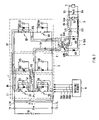
- FIG. 1 is a circuit diagram showing the configuration of a switching power supply unit according to a first embodiment of the invention.
- FIG. 2 is a timing waveform chart illustrating operations of the switching power supply unit of FIG. 1 .
- FIG. 3 is a circuit diagram illustrating operations of the switching power supply unit of FIG. 1 .
- FIG. 4 is a circuit diagram illustrating operations of the switching power supply unit subsequent to FIG. 3 .
- FIG. 5 is a circuit diagram illustrating operations of the switching power supply unit subsequent to FIG. 4 .
- FIG. 6 is a circuit diagram illustrating operations of the switching power supply unit subsequent to FIG. 5 .
- FIG. 7 is a circuit diagram illustrating operations of the switching power supply unit subsequent to FIG. 6 .
- FIG. 8 is a circuit diagram illustrating operations of the switching power supply unit subsequent to FIG. 7 .
- FIG. 9 is a circuit diagram illustrating operations of the switching power supply unit subsequent to FIG. 8 .
- FIG. 10 is a circuit diagram illustrating operations of the switching power supply unit subsequent to FIG. 9 .
- FIG. 11 is a circuit diagram illustrating operations of the switching power supply unit subsequent to FIG. 10 .
- FIG. 12 is a circuit diagram illustrating operations of the switching power supply unit subsequent to FIG. 11 .
- FIG. 13 is a circuit diagram illustrating operations of the switching power supply unit subsequent to FIG. 12 .
- FIG. 14 is a circuit diagram illustrating operations of the switching power supply unit subsequent to FIG. 13 .
- FIG. 15 is a timing waveform chart illustrating operations of the switching power supply unit subsequent to FIG. 14 .
- FIGS. 16A , 16 B, and 16 C are timing waveform charts for comparing operations of switching power supply units of FIG. 1 and comparative examples 1 and 2.
- FIG. 17 is a circuit diagram showing the configuration of a switching power supply unit according to comparative example 1.
- FIG. 18 is a circuit diagram showing the configuration of a switching power supply unit according to comparative example 2.
- FIG. 19 is a circuit diagram showing the configuration of a switching power supply unit according to a modification of the embodiment.
- FIG. 20 is a circuit diagram showing the configuration of a rectifier circuit according to the modification of the first embodiment.
- FIG. 21 is a circuit diagram showing the configuration of a switching power supply unit according to another modification of the first embodiment.
- FIG. 22 is a circuit diagram showing the configuration of a switching power supply unit according to another modification of the first embodiment.
- FIG. 23 is a circuit diagram showing the configuration of a switching power supply unit according to another modification of the first embodiment.
- FIG. 24 is a circuit diagram showing the configuration of a switching power supply unit according to another modification of the first embodiment.
- FIG. 25 is a circuit diagram showing the configuration of a switching power supply unit according to another modification of the first embodiment.
- FIG. 26 is a circuit diagram showing the configuration of a switching power supply unit according to another modification of the first embodiment.
- FIG. 27 is a circuit diagram showing the configuration of a switching power supply unit according to another modification of the first embodiment.
- FIG. 28 is a circuit diagram showing the configuration of a switching power supply unit according to another modification of the first embodiment.
- FIG. 29 is a circuit diagram showing the configuration of a switching power supply unit according to a second embodiment of the invention.
- FIG. 30 is a characteristic diagram illustrating a switching operation control by a controller.
- FIG. 31 is a diagram illustrating the switching operation control by the controller.
- FIG. 32 is a flowchart of the switching operation control performed by the controller.
- FIG. 33 is a timing waveform chart illustrating operations of the switching power supply unit in the case of selectively operating a first bridge circuit.
- FIG. 34 is a circuit diagram illustrating operations of the switching power supply unit in the case of selectively operating the first bridge circuit.
- FIG. 35 is a circuit diagram illustrating operations of the switching power supply unit subsequent to FIG. 34 .
- FIG. 36 is a circuit diagram illustrating operations of the switching power supply unit subsequent to FIG. 35 .
- FIG. 37 is a circuit diagram illustrating operations of the switching power supply unit subsequent to FIG. 36 .
- FIG. 38 is a circuit diagram illustrating operations of the switching power supply unit subsequent to FIG. 37 .
- FIG. 39 is a circuit diagram illustrating operations of the switching power supply unit subsequent to FIG. 38 .
- FIG. 40 is a circuit diagram illustrating operations of the switching power supply unit subsequent to FIG. 39 .
- FIG. 41 is a circuit diagram illustrating operations of the switching power supply unit subsequent to FIG. 40 .
- FIG. 42 is a circuit diagram illustrating operations of the switching power supply unit subsequent to FIG. 41 .
- FIG. 43 is a circuit diagram illustrating operations of the switching power supply unit subsequent to FIG. 42 .
- FIG. 44 is a circuit diagram illustrating operations of the switching power supply unit subsequent to FIG. 43 .
- FIG. 45 is a circuit diagram illustrating operations of the switching power supply unit subsequent to FIG. 44 .
- FIG. 46 is a timing waveform chart illustrating operations of the switching power supply unit subsequent to FIG. 45 .
- FIGS. 47A , 47 B, and 47 C are timing waveform charts for comparing operations of switching power supply units of FIG. 29 and comparative examples 3 and 4.
- FIG. 48 is a circuit diagram showing the configuration of a switching power supply unit according to the comparative example 3.
- FIG. 49 is a circuit diagram showing the configuration of a switching power supply unit according to the comparative example 4.
- FIG. 50 is a timing waveform chart illustrating operations of the switching power supply unit in the case of selectively operating a second bridge circuit.
- FIG. 51 is a timing waveform chart illustrating the operations of the switching power supply unit subsequent to FIG. 50 .
- FIG. 52 is a characteristic diagram illustrating changes of an input voltage range in the case of selectively operating the second bridge circuit.
- FIG. 53 is a timing waveform chart illustrating operations of a switching power supply unit according to a modification of the second embodiment.
- FIG. 54 is a timing waveform chart illustrating the operations of the switching power supply unit subsequent to FIG. 53 .
- FIGS. 55A and 55B are characteristic diagrams illustrating the switching operation control according to a modification of the second embodiment.
- FIG. 56 is a circuit diagram showing the configuration of a switching power supply unit according to a modification of the second embodiment.
- FIG. 57 is a circuit diagram showing the configuration of a switching power supply unit according to another modification of the second embodiment.
- FIG. 58 is a circuit diagram showing the configuration of a switching power supply unit according to another modification of the second embodiment.
- FIG. 59 is a circuit diagram showing the configuration of a switching power supply unit according to another modification of the second embodiment.
- FIG. 60 is a circuit diagram showing the configuration of a switching power supply unit according to a third embodiment of the invention.
- FIG. 61 is a diagram illustrating the difference between forward-direction operation and reverse-direction operation.
- FIG. 62 is a timing waveform chart illustrating the forward-direction operation in the switching power supply unit of FIG. 60 .
- FIG. 63 is a circuit diagram illustrating the forward-direction operation in the switching power supply unit of FIG. 60 .
- FIG. 64 is a circuit diagram illustrating the forward-direction operation subsequent to FIG. 63 .
- FIG. 65 is a circuit diagram illustrating the forward-direction operation subsequent to FIG. 64 .
- FIG. 66 is a circuit diagram illustrating the forward-direction operation subsequent to FIG. 65 .
- FIG. 67 is a circuit diagram illustrating the forward-direction operation subsequent to FIG. 66 .
- FIG. 68 is a circuit diagram illustrating the forward-direction operation subsequent to FIG. 67 .
- FIG. 69 is a circuit diagram illustrating the forward-direction operation subsequent to FIG. 68 .
- FIG. 70 is a circuit diagram illustrating the forward-direction operation subsequent to FIG. 69 .
- FIG. 71 is a circuit diagram illustrating the forward-direction operation subsequent to FIG. 70 .
- FIG. 72 is a circuit diagram illustrating the forward-direction operation subsequent to FIG. 71 .
- FIG. 73 is a circuit diagram illustrating the forward-direction operation subsequent to FIG. 72 .
- FIG. 74 is a circuit diagram illustrating the forward-direction operation subsequent to FIG. 73 .
- FIG. 75 is a timing waveform chart illustrating the forward-direction operation subsequent to FIG. 74 .
- FIG. 76 is a timing waveform chart illustrating the reverse-direction operation in the switching power supply unit of FIG. 60 .
- FIG. 77 is a circuit diagram illustrating the reverse-direction operation in the switching power supply unit of FIG. 60 .
- FIG. 78 is a circuit diagram illustrating the reverse-direction operation subsequent to FIG. 77 .
- FIG. 79 is a circuit diagram illustrating the reverse-direction operation subsequent to FIG. 78 .
- FIG. 80 is a circuit diagram illustrating the reverse-direction operation subsequent to FIG. 79 .
- FIG. 81 is a circuit diagram illustrating the reverse-direction operation subsequent to FIG. 80 .
- FIG. 82 is a circuit diagram illustrating the reverse-direction operation subsequent to FIG. 81 .
- FIG. 83 is a circuit diagram illustrating the reverse-direction operation subsequent to FIG. 82 .
- FIG. 84 is a circuit diagram illustrating the reverse-direction operation subsequent to FIG. 83 .
- FIG. 85 is a circuit diagram illustrating the reverse-direction operation subsequent to FIG. 84 .
- FIG. 86 is a circuit diagram showing the configuration of a conventional bidirectional switching power supply unit.
- FIG. 87 is a circuit diagram showing the configuration of a switching power supply unit according to comparative example 5.
- FIG. 88 is a timing waveform chart illustrating the reverse-direction operation in the switching power supply unit according to the comparative example 5.
- FIGS. 89A and 89B are enlarged timing waveform charts for comparing reverse-direction operations in the switching power supply units in FIG. 60 and the comparative example 5.
- FIG. 90 is a circuit diagram showing the configuration of a switching power supply unit according to a modification of the third embodiment.
- FIG. 91 is a circuit diagram showing the configuration of a switching power supply unit according to another modification of the third embodiment.
- FIG. 92 is a circuit diagram showing the configuration of a switching power supply unit according to another modification of the third embodiment.
- FIG. 93 is a circuit diagram showing the configuration of a switching power supply unit according to another modification of the third embodiment.
- FIG. 94 is a circuit diagram showing the configuration of a switching power supply unit according to another modification of the third embodiment.
- FIG. 95 is a circuit diagram showing the configuration of a switching power supply unit according to another modification of the third embodiment.
- FIG. 96 is a circuit diagram showing the configuration of a switching power supply unit according to another modification of the third embodiment.
- FIG. 97 is a circuit diagram showing the configuration of a switching power supply unit according to another modification of the third embodiment.
- the first embodiment corresponds to a concrete example of a second switching power supply unit according to the invention.
- FIG. 1 shows a configuration of a switching power supply unit according to the first embodiment.
- the switching power supply unit functions as a DC-DC converter for converting a high DC input voltage Vin supplied from a high-voltage battery 10 to a lower DC output voltage Vout, and supplying the DC output voltage Vout to a not-shown low-voltage battery to drive a load 7 .
- the switching power supply unit has an input smoothing capacitor 11 , a bridge circuit 1 , a surge voltage suppressing circuit 2 which are provided between a primary high-voltage line L 1 H and a primary low-voltage line L 1 L, an inductor Lr for resonance, and a transformer 3 having a primary winding 31 and secondary windings 32 A and 32 B. Across an input terminal T 1 of the primary high-voltage line L 1 H and an input terminal T 2 of the primary low-voltage line L 1 L, the DC input voltage Vin output from the high-voltage battery 10 is applied.
- the switching power supply unit also has a rectifier circuit 4 provided on the secondary side of the transformer 3 , a smoothing circuit 5 connected to the rectifier circuit 4 , and a driving circuit 6 for driving the bridge circuit 1 .
- the input smoothing capacitor 11 is provided to smooth the DC input voltage Vin input from the input terminals T 1 and T 2 .
- the bridge circuit 1 has four switching elements S 1 to S 4 , and capacitors C 1 to C 4 and diodes D 1 to D 4 connected in parallel with the switching elements S 1 to S 4 , respectively, and has a full-bridge circuit configuration. Concretely, one end of the switching element S 1 and one end of the switching element S 2 are connected to each other, and one end of the switching element S 3 and one end of the switching element S 4 are connected to each other. The other ends of the switching elements S 1 and S 3 are connected to each other and connected to the input terminal T 1 , and the other ends of the switching elements S 2 and S 4 are connected to each other and connected to the input terminal T 2 . With such a configuration, the bridge circuit 1 converts the DC input voltage Vin applied across the input terminals T 1 and T 2 to an input AC voltage in accordance with drive signals SG 1 to SG 4 supplied from the driving circuit 6 .
- MOS-FETs Metal Oxide Semiconductor-Field Effect Transistors
- IGBTs Insulated Gate Bipolar Transistors
- MOS-FETs Metal Oxide Semiconductor-Field Effect Transistors
- IGBTs Insulated Gate Bipolar Transistors
- capacitors C 1 to C 4 and the diodes D 1 to D 4 parasitic capacitors or parasitic diodes of the MOS-FETs can be used.
- junction capacitance of the diodes D 1 to D 4 may be used. In the case of using such a configuration, it becomes unnecessary to provide the capacitors C 1 to C 4 and the diodes D 1 to D 4 separately from the switching elements, so that the circuit configuration can be simplified.
- the surge voltage suppressing circuit 2 has a pair of diodes D 5 and D 6 connected in opposite directions, and capacitors C 5 and C 6 connected in parallel with the diodes D 5 and D 6 , respectively.
- the anode of the diode D 5 is connected to a connection point P 3
- the cathode is connected to the primary high-voltage line L 1 H.
- the anode of the diode D 6 is connected to the primary low-voltage line L 1 L and the cathode is connected to the connection point P 3 .
- resonance time of the first resonance circuit and recovery time of the diodes 4 A and 4 B are set so as to satisfy the following conditional expression (1).
- the reverse voltages of the diodes 4 A and 4 B are subjected to resonance in a quarter of the resonance time and gently reach a voltage according to the turn ratio of the input voltage. During the period, recovery gently finishes.
- the surge voltage applied to the diodes 4 A and 4 B is suppressed.
- Trr 1 indicates recovery time of the diodes 4 A and 4 B.
- the recover time denotes as follows.
- the diodes 4 A and 4 B are PN junction diodes, the diodes are in a conductive state because of holes injected from a P layer to an N layer. However, in a process that the forward current decreases and the reverse voltage is applied, the holes accumulated in the N layer return to the P layer or recombine and disappear.
- the current flows in the opposite direction in the diodes 4 A and 4 B until a depletion layer extends.
- the current is called recovery current.
- the time in which the recovery current flows is called recover time.
- the recovery current is not generated in principle.
- the junction capacitance exists also in this case. In the process in which the reverse voltage is applied, while charging the junction capacitance, the current flows in the opposite direction. Therefore, in the case of the schottky-barrier diodes, it can be considered that the time in which the current in the opposite direction flows corresponds to the recovery time.
- the inductor Lr is connected so as to form an H bridge to the bridge circuit constructed by the switching elements S 1 and S 2 , the diodes D 5 and D 6 , and the capacitors C 5 and C 6 .
- the inductor Lr and the capacitors C 1 to C 4 in the bridge circuit 1 construct an LC series resonance circuit (second resonance circuit).
- the inductor Lr and the capacitors C 5 and C 6 in the surge voltage suppressing circuit 2 construct the LC series resonance circuit (first resonance circuit), and a surge voltage applied to the diodes 4 A and 4 B in the rectifier circuit 4 is suppressed.
- the inductance of the inductor Lr is set so as to be much smaller than that of the primary winding 31 of the transformer 3 which will be described later.
- the transformer 3 has the primary winding 31 and the pair of secondary windings 32 A and 32 B.
- One end of the primary winding 31 is connected to the connection point P 3 , and the other end is connected to a connection point P 2 .
- the primary winding 31 is connected so as to form an H bridge to the bridge circuit constructed by the switching elements S 3 and S 4 , the diodes D 5 and D 6 , and the capacitors C 5 and C 6 .
- one ends of the secondary windings 32 A and 32 B are connected to each other at a center tap CT.
- the center tap CT is led along an output line LO to an output terminal T 3 via the smoothing circuit 5 . That is, the rectifier circuit 4 which will be described later is of a center tap type.
- the transformer 3 drops the input AC voltage generated by the bridge circuit 1 and outputs output AC voltages whose phases are different from each other by 180 degrees from the ends of the secondary windings 32 A and 32 B.
- the degree of voltage drop in this case is determined by the turn ratio between the primary winding 31 and the secondary windings 32 A and 32 B.
- the rectifier circuit 4 is a single-phase full-wave rectifier constructed by the pair of diodes 4 A and 4 B.
- the cathode of the diode 4 A is connected to the other end of the secondary winding 32 A of the transformer 3
- the cathode of the diode 4 B is connected to the other end of the secondary winding 32 B of the transformer 3 .
- the anodes of the diodes 4 A and 4 B are connected to each other and connected to a ground line LG. That is, the rectifier circuit 4 has a center-tap-type anode-common-connection configuration.
- the rectifier circuit 4 rectifies a half wave period of the output AC voltage from the transformer 3 by the diode 4 A and rectifies the other half wave period by the diode 4 B to obtain DC voltage.
- Each of the diodes 4 A and 4 B may be constructed by a parasitic diode of a MOS-FET.
- the MOS-FETs are turned on synchronously with periods in which the parasitic diodes of the MOS-FETs are made conductive for the reason that the voltages can be rectified with a smaller voltage drop.
- the smoothing circuit 5 includes a choke coil 51 and an output smoothing capacitor 52 .
- the choke coil 51 is inserted in the output line LO.
- One end of the choke coil 51 is connected to the center tap CT and the other end of the choke coil 51 is connected to the output terminal T 3 of the output line LO.
- the smoothing capacitor 52 is connected between the output line LO (concretely, the other end of the choke coil 51 ) and the ground line LG.
- An output terminal T 4 is provided at an end of the ground line LG.
- the driving circuit 6 is provided to drive the switching elements S 1 to S 4 in the bridge circuit 1 . Concretely, the driving circuit 6 supplies the drive signals SG 1 to SG 4 to the switching elements S 1 to S 4 to turn on/off the switching elements S 1 to S 4 . The driving circuit 6 performs phase control on the switching elements S 1 to S 4 as will be described later to properly set the phase differences, thereby stabilizing the DC output voltage Vout.
- the capacitors C 1 to C 4 correspond to a concrete example of “second capacitative elements” in the invention.
- the inductor Lr corresponds to a concrete example of “resonance inductor” in the invention.
- the diodes 4 A and 4 B correspond to a concrete example of “first rectifier elements”.
- the capacitors C 5 and C 6 correspond to a concrete example of “first capacitative elements” in the invention.
- the diodes D 5 and D 6 correspond to a concrete example of “second rectifier elements” in the invention.
- Each of the set of the capacitor C 5 and the diode D 5 and the set of the capacitor C 6 and the diode D 6 corresponds to a concrete example of “device set” in the invention.
- the switching elements S 3 and S 4 correspond to a concrete example of “two switching elements” in the invention, and the switching elements S 1 and S 2 correspond to a concrete example of “the other two switching elements” in the invention.
- the bridge circuit 1 switches the DC input voltage Vin supplied from the high-voltage battery 10 via the input terminals T 1 and T 2 , thereby generating an input AC voltage, and supplies the input AC voltage to the primary winding 31 of the transformer 3 . From the secondary windings 32 A and 32 B of the transformer 3 , an output AC voltage transformed (in this case, dropped) is obtained.
- the rectifier circuit 4 rectifies the output AC voltage by the diodes 4 A and 4 B. As a result, a rectified output is generated between the center tap CT (output line LO) and the connection point (ground line LG) of the diodes 4 A and 4 B.
- the smoothing circuit 5 smoothes the rectified output generated between the center tap CT and the diodes 4 A and 4 B, and outputs the DC output voltage Vout from the output terminals T 3 and T 4 .
- the DC output voltage Vout is supplied to a not-shown low-voltage battery and the load 7 is driven.
- FIGS. 2 to 15 the operation of suppressing the surge voltage applied to the diodes 4 A and 4 B in the rectifier circuit 4 as main characteristics of the invention will be described in detail.
- FIG. 2 is a timing waveform chart (times t 0 to t 10 ) of voltage waveforms and current waveforms of parts in the switching power supply unit of FIG. 1 .
- (A) to (D) in the diagram show voltage waveforms of the drive signals SG 1 to SG 4 .
- (E) to (G) show potentials VP 1 to VP 3 at the connection points P 1 to P 3 .
- (H) shows the potential difference V P1 ⁇ P3 between the connection points P 1 and P 3 when the potential VP 3 at the connection point P 3 is used as a reference.
- (I) shows the potential difference V P3 ⁇ P2 between the connection points P 3 and P 2 when the potential VP 2 at the connection point P 2 is used as a reference.
- (J) indicates current Ir flowing in the inductor Lr.
- (K) indicates current I 31 flowing in the primary winding 31 of the transformer 3 .
- (L) and (M) indicate currents I 5 and I 6 flowing in parallel connection parts between the diodes D 5 and D 6 and the capacitors C 5 and C 6 , respectively, in the surge voltage suppressing circuit 2 .
- (N) and (P) indicate reverse voltages V 4 A and V 4 B applied across the anodes and cathodes of the diodes 4 A and 4 B, respectively.
- (O) and (Q) denote currents I 4 A and I 4 B flowing in the diodes 4 A and 4 B, respectively.
- (R) denotes current I 51 flowing in the choke coil 51 .
- the directions of the voltages are as shown by the arrows in FIG. 1 .
- the direction from “ ⁇ ” to “+” is a positive direction.
- the positive directions of the currents are also as shown by the arrows in FIG. 1 .
- FIGS. 3 to 14 show operation states of the switching power supply unit at the timings (times t 0 to t 10 ) in FIG. 2 .
- FIG. 15 shows voltage waveforms and current waveforms in parts after the timings illustrated in FIG. 2 (times t 10 to t 20 (t 0 )).
- the timings shown in FIGS. 2 and 15 correspond to half cycles of the operation in the switching power supply unit. Combination of the operations corresponds to operations in one cycle.
- the switching elements S 1 to S 4 are paired.
- the switching elements S 1 and S 2 are controlled to be turned on at fixed timings on the time base and are therefore called “fixed-side switching elements”.
- the switching elements S 3 and S 4 are controlled to be turned on at variable timings on the time base and are therefore called “shift-side switching elements”.
- the switching elements S 1 to S 4 are driven at timings and in combinations that the input terminals T 1 and T 2 to which the DC input voltage Vin is applied are not electrically short-circuited in any state of the switching operation. Concretely, the switching elements S 3 and S 4 (fixed-side switching elements) are not turned on simultaneously, and the switching elements S 1 and S 2 (shift-side switching elements) are not also turned on simultaneously. A time interval required to avoid simultaneous turn-on of the switching elements is called dead time “Td” ((A) and (D) in FIG. 2 ).
- the switching elements S 1 and S 4 have a period in which they are on simultaneously. In the period in which the switching elements S 1 and S 4 are simultaneously on, the primary winding 31 of the transformer 3 is excited.
- the switching elements S 1 and S 4 operate so as to have a switching phase difference ⁇ by using the switching element S 1 (fixed-side switching element) as a reference ((A) and (D) in FIG. 2 ).
- the switching elements S 2 and S 3 have a period in which they are simultaneously on. In the period in which they are simultaneously on, the primary winding 31 of the transformer 3 is excited in the direction opposite to that in the above case.
- the switching elements S 2 and S 3 operate so as to have a switching phase difference ⁇ by using the switching element S 2 (fixed-side switching element) as a reference ((B) and (C) in FIG. 2 ). Further, when the switching phase difference ⁇ between the switching elements S 1 and S 4 and the switching phase difference ⁇ between the switching elements S 2 and S 3 are controlled, the time in which the switching elements S 1 and S 4 are simultaneously on and the time in which the switching elements S 2 and S 3 are simultaneously on change, respectively. Accordingly, the duty ratio of the input AC voltage applied to the primary winding 31 of the transformer 3 changes, and the DC output voltage Vout is stabilized.
- the switching elements S 1 and S 4 are in the on state ((A) and (D) in FIG. 2 ), and the switching elements S 2 and S 3 are in the off state ((B) and (C) in FIG. 2 ).
- the inductance of the inductor Lr is much smaller than that of the primary winding 31 of the transformer 3 , so that the potential VP 3 at the connection point P 3 is almost equal to Vin ((G) in FIG. 2 ), and the potential difference V P3 ⁇ P2 between the connection points P 3 and P 2 using VP 2 as a reference is also almost equal to Vin ((I) in FIG. 2 ). Therefore, a loop current Ia as shown in FIG. 3 flows in the bridge circuit 1 , so that the inductor Lr is exited and power is transmitted from the primary side to the secondary side of the transformer 3 . A loop current Ixa flows to the secondary side of the transformer 3 via the diode 4 A and the choke coil 51 , and the load 7 is driven. In the period, forward voltage is applied to the diode 4 A and the reverse voltage V 4 A becomes 0V ((N) in FIG. 2 ). To the other diode 4 B, the reverse voltage V 4 B is applied ((P) in FIG. 2 ).
- the switching element S 4 is turned off at the time t 1 ((D) in FIG. 2 ).
- the LC series resonance circuit (second resonance circuit) is constructed by cooperation of the capacitors C 3 and C 4 and the inductor Lr, and second resonance operation is performed. Therefore, the loop currents Ib and Ic as shown in FIG. 4 flow, the capacitor C 3 is discharged and, on the other hand, the capacitor C 4 is charged. Consequently, the potential VP 2 at the connection point P 2 gradually increases and becomes equal to Vin at the time t 2 ((F) in FIG. 2 ). At this time, the reverse voltage V 4 B of the diode 4 B drops gradually and becomes 0V at the time t 2 ((P) in FIG. 2 ).
- V 31 is equal to a value obtained by dividing a forward voltage drop in the diode 4 A by the turn ratio “n”.
- V 31 is a forward voltage drop in the diode D 3 when the switching element S 3 is off (the period from time t 2 to time t 3 ).
- V 31 is the product between the on resistance of the switching element S 3 and flowing current when the switching element S 3 is on (the period from time t 3 to time t 4 ).
- the potential difference is a forward voltage drop in the diode D 5 .
- the loop currents Id and Ie flow so that the potential differences become equal to each other.
- the absolute value of the current I 31 flowing in the primary winding 31 of the transformer 3 decreases ((K) in FIG. 2 ).
- the current I 51 is branched to the loop current Ixa flowing in the diode 4 A and the loop current Ixb flowing in the diode 4 B so that the sum of the currents flowing in the secondary windings 32 A and 32 B of the transformer 3 becomes equal to the current I 51 flowing in the chock coil 51 .
- the switching element S 1 is turned off ((A) in FIG. 2 ). It makes the capacitors C 1 and C 2 and the inductor Lr cooperate with one another to construct the LC series resonance circuit (second resonance circuit) and the second resonance operation is performed. Therefore, the loop currents If, Ig, Ih, and Ii as shown in FIG. 7 flow.
- the energy accumulated in the inductor Lr is regenerated in the input smoothing capacitor 11 by the loop currents Im and I 1 as shown in FIG. 9 after charging/discharging in the capacitors C 1 and C 2 is completed.
- the energy accumulated in the inductor Lr decreases.
- the absolute value of the current Ir flowing in the inductor Lr and the absolute value of the current I 31 flowing in the primary winding 31 of the transformer 3 also decrease ((J) and (K) in FIG. 2 ).
- the current I 51 is branched to the loop current Ixa flowing in the diode 4 A and the loop current Ixb flowing in the diode 4 B so that the ampere turns in the transformer 3 become equal to each other and the sum of currents flowing in the secondary windings 32 A and 32 B in the transformer 3 becomes equal to the current I 51 flowing in the choke coil 51 .
- the loop currents Im and I 1 flow so that the potential differences from one end (the connection point P 3 ) of the inductor Lr to the cathode of the diode D 5 become equal to each other.
- the potential difference in the path of the loop current Im becomes larger than that in the path of the loop current I 1 , and the diode D 5 becomes nonconductive. It makes the absolute value of the current Ir flowing in the inductor Lr and that of the current I 31 flowing in the primary winding 31 of the transformer 3 equal to each other ((J) and (K) in FIG. 2 ).
- the potential difference in the path of the loop current I 1 is equal to the sum of the voltage V 31 across the primary winding 31 of the transformer 3 and the voltage VS 3 across the switching element S 3 .
- the voltage V 31 is a voltage value obtained by dividing the forward voltage drop in the diode 4 A by the turn ratio “n” between the primary winding and the secondary winding of the transformer 3 .
- the voltage VS 3 is equal to the product between the on resistance of the switching element S 3 and the flowing current since the switching element S 3 is in the on state in this period.
- the potential difference in the path of the loop current Im is the forward voltage drop in the diode D 5 .
- each of the current Ir flowing in the inductor Lr and the current I 31 flowing in the primary winding 31 of the transformer 3 is equal to 0 A ((J) and (K) in FIG. 2 ).
- the current I 4 A flowing in the diode 4 A is equal to the current I 4 B flowing in the diode 4 B ((O) and (Q) in FIG. 2 ).
- the inductor Lr accumulates energy in the direction opposite to the accumulation direction until then.
- the loop current In in the opposite direction flows in the inductor Lr and the primary winding 31 of the transformer 3 as shown in FIG.
- the current Ir increases at the rate of Vin/L (L: inductance of the inductor Lr) ((J) and (K) in FIG. 2 ). Consequently, the current I 51 is branched to the loop current Ixa flowing in the diode 4 A and the loop current Ixb flowing in the diode 4 B so that the ampere turns in the transformer 3 become equal to each other and the sum of currents flowing in the secondary windings 32 A and 32 B in the transformer 3 becomes equal to the current I 51 flowing in the choke coil 51 .
- the current I 4 A flowing in the diode 4 A gradually decreases and, on the other hand, the current I 4 B flowing in the diode 4 B gradually increases ((O) and (Q) in FIG. 2 ).
- the timing when VP 3 decreases gently and becomes 0V and V P3 ⁇ P2 ⁇ Vin ((G) and (I) in FIG. 2 ) corresponds to time t 9 .
- resonance time of the first resonance circuit and the recovery time of the diodes 4 A and 4 B are set so as to satisfy the conditional expression (1), so that generation of the recovery current in the diodes 4 A and 4 B is suppressed. Therefore, the first resonance operation performed by the capacitors C 5 and C 6 and the inductor Lr is to be continued.
- VP 3 is equal to 0V ((G) in FIG. 2 )
- the voltage across the capacitor C 6 and the diode D 6 becomes 0V.
- the current IC 6 flowing in the capacitor C 6 becomes 0V and the diode D 6 is made conductive.
- the diode D 6 is conductive and the switching element S 3 is in the on state ((C) in FIG. 2 ). Consequently, the voltage V 31 across the primary winding 31 of the transformer 3 (and the absolute value of VP 3 ⁇ P2 ((I) in FIG. 2 ) is clamped at Vin so that the voltage V 32 B across the secondary winding 32 B of the transformer 3 is clamped at Vin/n (n: the turn ratio between the primary winding and the secondary winding of the transformer 3 ). Since the rectifier circuit 4 is of the center tap type, the reverse voltage V 4 A applied to the diode 4 A does not exceed 2 ⁇ Vin/n ((N) in FIG. 2 ). In other words, the reverse voltage V 4 A applied to the diode 4 A is 2 ⁇ Vin/n at the maximum, so that rise in the surge voltage is suppressed.
- the resonance current generated by the first resonance operation is expressed by the loop current Iq as shown in FIG. 13 while Ir becomes constant ((J) in FIG. 2 ).
- the choke coil 51 is excited by the voltage V 32 B across the secondary winding 32 B of the transformer 3 , the current I 51 flowing in the chock coil 51 increases.
- the operations in the half cycle are basically similar to those in the half cycle described with reference to FIGS. 2 to 14 .
- the switching elements S 2 and S 3 are in the on state ((B) and (C) in FIG. 15 ), and the switching elements S 1 and S 4 are in the off state ((A) and (D) in FIG. 15 ).
- the potential VP 1 at the connection point P 1 is equal to 0V ((E) in FIG. 15 )
- the potential VP 2 at the connection point P 2 is equal to Vin ((F) in FIG. 15 )
- the inductance of the inductor Lr is much smaller than that of the primary winding 31 of the transformer 3 .
- the potential VP 3 at the connection point P 3 becomes almost 0V ((G) in FIG. 15 ), and the potential difference V P3 ⁇ P2 between the connection points P 3 and P 2 when VP 2 is used as a reference is almost equal to 0V ((I) in FIG. 15 ). Therefore, the loop current flows in the bridge circuit 1 , the inductor Lr is excited, and power is transmitted from the primary side to the secondary side in the transformer 3 . Thus, the loop current flows to the secondary side of the transformer 3 via the diode 4 B and the choke coil 51 , and the load 7 is driven. In the period, the forward voltage is applied to the diode 4 B, and the reverse voltage V 4 B is equal to 0V ((P) in FIG. 15 ). On the other hand, the reverse voltage V 4 A is applied to the diode 4 A ((N) in FIG. 15 ).
- the switching element S 3 is turned off at the time t 11 ((C) in FIG. 15 ).
- the capacitors C 3 and C 4 and the inductor Lr cooperate one another to construct the LC series resonance circuit (second resonance circuit), and the second resonance operation is performed. Therefore, by the two loop currents, the capacitor C 3 is charged and, on the other hand, the capacitor C 4 is discharged.
- the reverse voltage V 4 A of the diodes 4 A decreases gradually and becomes 0V at the time t 12 ((N) in FIG. 15 ).
- the current I 51 flowing in the choke coil 51 is branched to the loop current Ixa flowing in the diode 4 A and the loop current Ixb flowing in the diode 4 B so that the ampere turns in the transformer 3 become equal to each other and the sum of the currents flowing in the secondary windings 32 A and 32 B in the transformer 3 becomes equal to the current I 51 .
- the switching element S 2 is turned off ((B) in FIG. 15 ).
- the LC series resonance circuit (second resonance circuit) is constructed by cooperation of the capacitors C 1 and C 2 and the inductor Lr, and second resonance operation is performed. Therefore, four loop currents flow, the capacitor C 2 is charged and, on the other hand, the capacitor C 1 is discharged. Consequently, the potential VP 1 at the connection point P 1 gradually increases and becomes equal to Vin at the time t 15 ((E) in FIG. 15 ).
- the energy accumulated in the inductor Lr is regenerated in the input smoothing capacitor 11 by the two loop currents also after charging/discharging in the capacitors C 1 and C 2 is completed.
- the energy accumulated in the inductor Lr decreases.
- the absolute value of the current Ir flowing in the inductor Lr and the absolute value of the current I 31 flowing in the primary winding 31 of the transformer 3 also decrease ((J) and (K) in FIG. 15 ).
- the current I 51 is branched to the loop current Ixa flowing in the diode 4 A and the loop current Ixb flowing in the diode 4 B so that the ampere turns in the transformer 3 become equal to each other and the sum of currents flowing in the secondary windings 32 A and 32 B in the transformer 3 becomes equal to the current I 51 flowing in the choke coil 51 .
- the diode D 6 since the diode D 6 is nonconductive, the absolute value of the current Ir flowing in the inductor Lr and that of the current I 31 flowing in the primary winding 31 in the transformer 3 become equal to each other ((J) and (K) in FIG. 15 ).
- each of the current Ir flowing in the inductor Lr and the current I 31 flowing in the primary winding 31 of the transformer 3 is equal to 0 A ((J) and (K) in FIG. 15 ).
- the current I 4 A flowing in the diode 4 A is equal to the current I 4 B flowing in the diode 4 B ((O) and (Q) in FIG. 15 ).
- the inductor Lr accumulates energy in the direction opposite to the accumulation direction until then.
- the loop current In in the opposite direction flows in the inductor Lr and the primary winding 31 of the transformer 3 , and the current Ir increases at the rate of Vin/L (L: inductance of the inductor Lr) ((J) and (K) in FIG. 15 ). Consequently, the current I 51 flowing in the choke coil 51 is branched to the loop current Ixa flowing in the diode 4 A and the loop current Ixb flowing in the diode 4 B so that the ampere turns in the transformer 3 become equal to each other and the sum of currents flowing in the secondary windings 32 A and 32 B in the transformer 3 becomes equal to the current I 51 flowing in the choke coil 51 .
- the current I 4 B flowing in the diode 4 B gradually decreases and, on the other hand, the current I 4 A flowing in the diode 4 A gradually increases ((O) and (Q) in FIG. 15 ).
- the current I 4 B becomes equal to 0 A and the current flowing in the secondary winding 32 A in the transformer 3 becomes equal to the current I 51 flowing in the chock coil 51 , since the ampere turns in the transformer 3 do not increase any more, increase in the current I 31 is disturbed.
- the capacitors C 5 and C 6 in the surge voltage suppressing circuit 2 and the inductor Lr cooperate one another to construct the LC series resonance circuit (first resonance circuit), and first resonance operation starts. This timing corresponds to time t 18 .
- resonance time of the first resonance circuit and the recovery time of the diodes 4 A and 4 B are set so as to satisfy the conditional expression (1), so that generation of the recovery current in the diodes 4 A and 4 B is suppressed. Therefore, the first resonance operation performed by the capacitors C 5 and C 6 and the inductor Lr is to be continued.
- VP 3 is equal to Vin ((G) in FIG. 15 )
- the voltage across the capacitor C 5 and the diode D 5 becomes 0V.
- the current IC 5 flowing in the capacitor C 5 becomes 0 A and the diode D 5 is made conductive.
- the diode D 5 is conductive and the switching element S 4 is in the on state ((D) in FIG. 15 ). Consequently, the voltage V 31 across the primary winding 31 of the transformer 3 (and the absolute value of V P3 ⁇ P2 ((I) in FIG. 15 )) is clamped at Vin so that the voltage V 32 A across the secondary winding 32 A of the transformer 3 is clamped at Vin/n (n: the turn ratio between the primary winding and the secondary winding of the transformer 3 ). Since the rectifier circuit 4 is of the center tap type, the reverse voltage V 4 B applied to the diode 4 B does not exceed 2 ⁇ Vin/n ((P) in FIG. 15 ). In other words, the reverse voltage V 4 B applied to the diode 4 B is 2 ⁇ Vin/n at the maximum, so that rise in the surge voltage is suppressed.
- the diode D 5 is conductive as described above, so that Ir is constant ((J) in FIG. 15 ).
- the choke coil 51 is excited by the voltage V 32 A across the secondary winding 32 A of the transformer 3 , the current I 51 flowing in the chock coil 51 increases and I 31 also increases ((K) in FIG. 15 ). Since Ir is equal to I 31 +ID 5 and Ir is constant, as I 31 increases, ID 5 decreases.
- the operations in the latter half cycle have been described above and a state equivalent to that at the time t 0 in FIG. 2 is obtained.
- FIGS. 16A to 16C show timing waveforms of reverse voltages applied to the diodes in the switching power supply units of the embodiment and the comparative examples 1 and 2.
- FIGS. 17 and 18 show the configurations of the switching power supply units of the comparative examples 1 and 2, respectively.
- a surge voltage suppressing circuit 102 obtained by eliminating the capacitors C 5 and C 6 from the surge voltage suppressing circuit 2 is provided in the comparative example 1.
- a snubber circuit 202 for suppressing surge voltage constructed by an inductor L 7 , a capacitor C 7 , and a diode D 7 is provided on the secondary side of the transformer 3 in place of the surge voltage suppressing circuit 2 .
- one end of the inductor L 7 is connected between the choke coil 51 and the center tap CT on the output line LO, and the other end is connected to the cathode of the diode D 7 and one end of the capacitor C 7 .
- the anode of the diode D 7 is connected between the choke coil 51 and the center tap CT on the output line LO, and the other end of the capacitor C 5 is connected to the ground line LG.
- the reverse voltage waveforms shown in FIGS. 16A to 16C are voltage waveforms at the center tap CT on the secondary side of the transformer 3 , and a reverse voltage actually applied to the diodes 4 A and 4 B is a value twice as large as that shown in FIGS. 16A to 16C .
- the maximum value (peak value) of the surge voltage is 83V. This is a result of suppressing the surge voltage to some extent by the snubber circuit 202 and corresponds to about twice (2.02 times) as large as the DC input voltage Vin/n (n: the turn ratio between the primary winding and the secondary winding of the transformer 3 ).
- the maximum value of the surge voltage is 52V and corresponds to 1.26 times as large as Vin/n.
- the rise time to the maximum value is about 20 ns. It is understood that the reverse voltage rises abruptly due to the configuration that no capacitor is included in the surge voltage suppressing circuit 102 .
- the capacitors C 5 and C 6 are included in the surge voltage suppressing circuit 2 and the resonance time of the first resonance circuit constructed by the capacitors C 5 and C 6 and the inductor Lr and the recovery time of the diodes 4 A and 4 B are set so as to satisfy the conditional expression (1), as described above, it is understood that generation of the recovery currents in the diodes 4 A and 4 B is suppressed and the reverse voltage rises gently by the resonance operation of the first resonance circuit.
- the maximum value of the surge voltage is 45.5V and corresponds to about the same (1.08 times) as Vin/n, and the rise time to the maximum value is about 100 ns. It is understood that the rise of the reverse voltage is gentler than that in the comparative examples 1 and 2 shown in FIGS. 16B and 16C and, as a result, rise of the surge voltage is suppressed more effectively.
- the first resonance circuit is constructed by the capacitors C 5 and C 6 in the surge voltage suppressing circuit 2 and the inductor Lr and the resonance time of the first resonance circuit and the recovery time of the diodes 4 A and 4 B in the rectifier circuit 4 are set so as to satisfy the conditional expression (1). Consequently, rise of the reverse voltage applied to the diodes 4 A and 4 B can be made gentler than that in the conventional technique. Without depending on the configuration, the rise of the surge voltage can be suppressed more effectively.
- the maximum value (peak value) of the surge voltage can be suppressed to 2 ⁇ Vin/n (n: turn ratio between the primary winding and the secondary winding of the transformer 3 ).
- the maximum value can be suppressed more.
- a low-withstand-voltage rectifier element (diode) can be used, and the parts cost can be reduced.
- the surge voltage can be suppressed without depending on the unit configuration, the flexibility in the unit designing can be improved.
- the resonance time of the first resonance circuit and the recovery time Trr 2 of the diodes D 5 and D 6 in the surge voltage suppressing circuit 2 so as to satisfy not only the conditional expression (1) described in the embodiment but also the following conditional expression (2).
- the reverse voltage applied to the diodes D 5 and D 6 in addition to the diodes 4 A and 4 B reaches the input voltage gently in accordance with resonance in a quarter of the resonance time.
- recover is finished gently, so that rise in the surge voltage in the diodes D 5 and D 6 is also suppressed. Therefore, occurrence of ringing by the reverse voltage applied to the diodes D 5 and D 6 can be suppressed so that occurrence of noise can be also suppressed.
- the inductor Lr, the transformer 3 , and the circuits (the rectifier circuit 4 and the smoothing circuit 5 ) on the secondary side of the transformer 3 in the switching power supply unit ( FIG. 2 ) of the embodiment can change their sides with respect to the surge voltage suppressing circuit 2 as a center.
- the inductor Lr may be disposed between the connection points P 2 and P 3
- the transformer 3 may be disposed between the connection points P 1 and P 3 .
- effects similar to those of the embodiment can be obtained.
- the rectifier circuit 4 of the center tap type may be replaced with a rectifier circuit 41 of the full bridge type.
- a transformer 33 having a primary winding 331 and a secondary winding 332 is provided in placed of the transformer 3 in FIG. 1 , and the rectifier circuit 41 of the full bridge type including four diodes 41 A to 41 D is provided on the secondary side of the transformer 33 .
- the maximum value (peak value) of the surge voltage applied to the diodes 41 A to 41 D can be suppressed to 1 ⁇ Vin/n (n: turn ratio between the primary winding and the secondary winding of the transformer 3 ), which is lower than that in the conventional full-bridge type in which the maximum value is about 2 ⁇ Vin/n.
- the diodes 41 A to 41 D can be also constructed by parasitic diodes of MOS-FETs.
- the transformer 3 and the inductor Lr are provided magnetically independently of each other. It is also possible to provide, for example, as shown in FIGS. 21 and 22 , an auxiliary winding 31 B of the transformer 3 on the primary side of the transformer 3 .
- the auxiliary winding 31 B and the transformer 3 are magnetically coupled to each other (they share a magnetic flux (magnetic path)) as shown by reference numerals M 1 and M 2 in the diagram.
- the inductor Lr is disposed between the connection points P 1 and P 2
- the auxiliary winding 31 B of the transformer 3 is connected between the connection points P 1 and P 3 or between the connection points P 1 and P 2 . Since each of the above-described configurations shown in FIGS. 21 and 22 is equivalent to the configuration shown in FIG. 1 or 19 , effects similar to those of the embodiment can be obtained.
- surge voltage suppressing circuits 21 and 22 may be provided in place of the surge voltage suppressing circuit 2 .
- a device set of the diode D 5 and the capacitor C 5 and a device set of the diode D 6 and the capacitor C 6 may be connected in parallel with each other between the primary high-voltage line L 1 H and the primary low-voltage line L 1 L, and the auxiliary winding 31 B and an auxiliary winding 31 C of the transformer 3 may have a configuration of the center tap type (the auxiliary windings 31 B and 31 C are magnetically coupled to the transformer 3 as shown by the reference numerals M 3 and M 4 in the diagrams).
- auxiliary windings 31 B and 31 C are magnetically coupled to the transformer 3 are shown in FIGS. 21 to 24 , in addition, the auxiliary windings 31 B and 31 C may be magnetically coupled to the inductor Lr for resonance. This case is similarly effective.
- the inductor Lr for resonance may be provided on the secondary side of the transformer 3 .
- a pair of inductors LrA and LrB magnetically coupled to each other may be provided between the cathodes of the diodes 4 A and 4 B in the rectifier circuit 4 of the center tap type and the secondary windings 32 A and 32 B of the transformer 3 .
- FIGS. 25 and 27 a pair of inductors LrA and LrB magnetically coupled to each other may be provided between the cathodes of the diodes 4 A and 4 B in the rectifier circuit 4 of the center tap type and the secondary windings 32 A and 32 B of the transformer 3 .
- the inductor Lr may be disposed between the connection point of the anode of the diode 41 A and the cathode of the diode 41 B and the connection point of the anode of the diode 41 C and the cathode of the diode 41 D.
- the transformer 3 may be magnetically coupled to the auxiliary windings 31 B and 331 B.
- the inductor Lr for resonance or the inductors LrA and LrB for resonance may be magnetically coupled to the auxiliary windings 31 B and 331 B.
- the second embodiment corresponds to a concrete example of a second switching power supply unit according to the present invention.
- FIG. 29 shows a configuration of a switching power supply unit according to the second embodiment.
- the switching power supply unit functions as a DC-DC converter for converting a high DC input voltage Vin supplied from the high-voltage battery 10 to a lower DC output voltage Vout, and supplying the DC output voltage Vout to a not-shown low-voltage battery to drive the load 7 .
- the switching power supply unit has the input smoothing capacitor 11 , a bridge circuit 1001 , and a surge voltage suppressing circuit 1002 which are provided between the primary-side high-voltage line L 1 H and the primary-side low-voltage line L 1 L, the inductor Lr for resonance, a transformer 1003 having the primary winding 31 and the secondary windings 32 A and 32 B, a rectifier circuit 1004 provided on the secondary side of the transformer 1003 , the smoothing circuit 5 connected to the rectifier circuit 1004 , and a driving circuit 1006 for driving the bridge circuit 1001 and the surge voltage suppressing circuit 1002 .
- the DC input voltage Vin output from the high-voltage battery 10 is applied across the input terminal T 1 of the primary-side high-voltage line L 1 H and the input terminal T 2 of the primary-side low-voltage line L 1 L.
- the switching power supply unit also has: an input voltage detection circuit 1061 and an input current detection circuit 1062 disposed on the primary side of the transformer 1003 and detecting the DC input voltage Vin and the input current Iin, respectively; and a controller 1063 for controlling switching operation in the bridge circuit 1001 and the surge voltage suppressing circuit 1002 via the driving circuit 1006 .
- the input smoothing capacitor 11 is provided to smooth the DC input voltage Vin input from the input terminals T 1 and T 2 .
- the bridge circuit 1001 has the four switching elements S 1 to S 4 , and device sets of the capacitors C 1 to C 4 connected in parallel with the switching elements S 1 to S 4 , respectively, and diodes D 1 to D 4 connected to the switching elements S 1 to S 4 in the opposite direction, respectively, and has a full-bridge circuit configuration.
- one end of the switching element S 1 and one end of the switching element S 2 are connected to each other, and one end of the switching element S 3 and one end of the switching element S 4 are connected to each other.
- the other ends of the switching elements S 1 and S 3 are connected to each other and connected to the input terminal T 1
- the other ends of the switching elements S 2 and S 4 are connected to each other and connected to the input terminal T 2 .
- the bridge circuit 1001 converts the DC input voltage Vin applied across the input terminals T 1 and T 2 to an input AC voltage in accordance with drive signals SG 1 to SG 4 supplied from the driving circuit 1006 .
- the bridge circuit 1001 corresponds to a concrete example of “first bridge circuit” in the invention.
- a device set of the switching element S 1 , the diode D 1 , and the capacitor C 1 , and a device set of the switching element S 2 , the diode D 2 , and the capacitor C 2 correspond to a concrete example of “a first group” in the invention.
- a device set of the switching element S 3 , the diode D 3 , and the capacitor C 3 and a device set of the switching element S 4 , the diode D 4 , and the capacitor C 4 correspond to a concrete example of “a second group” in the invention.
- the switching elements S 1 to S 4 are switching elements such as, for example, MOS-FETs (Metal Oxide Semiconductor-Field Effect Transistors), IGBTs (Insulated Gate Bipolar Transistors), or the like.
- MOS-FETs Metal Oxide Semiconductor-Field Effect Transistors
- IGBTs Insulated Gate Bipolar Transistors
- parasitic capacitors or parasitic diodes of the MOS-FETs can be used.
- junction capacitance of the diodes D 1 to D 4 may be used. In the case of using such a configuration, it becomes unnecessary to provide the capacitors C 1 to C 4 and the diodes D 1 to D 4 separately from the switching elements, so that the circuit configuration can be simplified.
- the surge voltage suppressing circuit 1002 has two device sets; a device set of the switching element S 5 , the capacitor C 5 connected in parallel with the switching element S 5 , and the diode D 5 connected to the switching element S 5 in the opposite direction, and a device set of the switching element S 6 , the capacitor C 6 connected in parallel with the switching element S 6 , and the diode D 6 connected to the switching element S 6 in the opposite direction.
- the device sets are connected to each other in series. Concretely, the anode of the diode D 5 is connected to the connection point P 3 , and the cathode is connected to the primary-side high-voltage line L 1 H.
- the anode of the diode D 6 is connected to the primary-side low-voltage line L 1 L and the cathode is connected to the connection point P 3 .
- the capacitors C 5 and C 6 and the inductor Lr which will be described later construct an LC series resonance circuit (second resonance circuit).
- resonance time of the second resonance circuit and recovery time of the diodes 4 A and 4 B are set so as to satisfy the following conditional expression (3).
- the reverse voltages of the diodes 4 A and 4 B are subjected to resonance in a quarter of the resonance time and gently reach a voltage according to the turn ratio of the input voltage. During the period, recovery gently finishes.
- the surge voltage applied to the diodes 4 A and 4 B is suppressed. 1 ⁇ 4 ⁇ 2 ⁇ (L ⁇ C) 1/2 ⁇ >Trr 3 (3)
- Trr 3 indicates recovery time of the diodes 4 A and 4 B.
- the recover time denotes time as described below.
- the diodes 4 A and 4 B are PN junction diodes, the diodes are in a conductive state because of holes injected from a P layer to an N layer.
- the holes accumulated in the N layer return to the P layer or recombine and disappear.
- the current is called recovery current.
- the time in which the recovery current flows is called recover time.
- the recovery current is not generated in principle.
- the junction capacitance exists also in this case.
- the reverse voltage while charging the junction capacitance, the current flows in the opposite direction. Therefore, in the case of the schottky-barrier diodes, it can be considered that the time in which the current in the opposite direction flows corresponds to the recovery time.
- the surge voltage suppressing circuit 1002 corresponds to a concrete example of a “third group” in the invention.
- the switching elements S 5 and S 6 for example, MOS-FETs, IGBTs, or the like are used.
- MOS-FETs MOS-FETs
- the capacitors C 5 and C 6 and the diodes D 5 and D 6 parasitic capacitors or parasitic diodes of the MOS-FETs can be used.
- junction capacitance of the diodes D 5 and D 6 may be used. In the case of using such a configuration, it becomes unnecessary to provide the capacitors C 5 and C 6 and the diodes D 5 and D 6 separately from the switching elements, so that the circuit configuration can be simplified.
- the inductor Lr is connected to the connection point P 1 of the device sets in the first group, and the other end is connected to the connection point P 3 of the device sets in the third group.
- the inductor Lr and the capacitors C 1 to C 4 in the bridge circuit 1001 construct an LC series resonance circuit (first resonance circuit).
- the inductor Lr and the capacitors C 5 and C 6 in the surge voltage suppressing circuit 1002 construct an LC series resonance circuit (second resonance circuit), and a surge voltage applied to the diodes 4 A and 4 B in the rectifier circuit 1004 is suppressed.
- the inductance of the inductor Lr is set so as to be much smaller than that of the primary winding 31 of the transformer 1003 which will be described later.
- the transformer 1003 has the primary winding 31 and the pair of secondary windings 32 A and 32 B.
- One end of the primary winding 31 is connected to the connection point P 3 of the device set in the third group, and the other end is connected to a connection point P 2 of the device set in the second group.
- one ends of the secondary windings 32 A and 32 B are connected to each other at the center tap CT.
- the center tap CT is led along the output line LO to the output terminal T 3 via the smoothing circuit 5 . That is, the rectifier circuit 1004 which will be described later is of a center tap type.
- the transformer 1003 drops the input AC voltage generated by the bridge circuit 1001 or the bridge circuit 1001 and the surge voltage suppressing circuit 1002 , and outputs output AC voltages whose phases are different from each other by 180 degrees from the ends of the secondary windings 32 A and 32 B.
- the degree of voltage drop in this case is determined by the turn ratio between the primary winding 31 and the secondary windings 32 A and 32 B.
- the rectifier circuit 1004 is a single-phase full-wave rectifier constructed by the pair of diodes 4 A and 4 B.
- the cathode of the diode 4 A is connected to the other end of the secondary winding 32 A of the transformer 1003 .
- the cathode of the diode 4 B is connected to the other end of the secondary winding 32 B of the transformer 1003 .
- the anodes of the diodes 4 A and 4 B are connected to each other and connected to the ground line LG. That is, the rectifier circuit 1004 has a center-tap-type anode-common-connection configuration.
- the rectifier circuit 1004 rectifies half wave periods of the output AC voltage from the transformer 1003 by the diodes 41 A and 41 B to obtain DC voltage.
- Each of the diodes 4 A and 4 B may be constructed by a parasitic diode of a MOS-FET.
- the MOS-FETs are turned on synchronously with periods in which the parasitic diodes of the MOS-FETs are made conductive for the reason that the voltages can be rectified with a smaller voltage drop.
- the smoothing circuit 5 includes the choke coil 51 and the output smoothing capacitor 52 .
- the choke coil 51 is inserted in the output line LO.
- One end of the choke coil 51 is connected to the center tap CT and the other end of the choke coil 51 is connected to the output terminal T 3 of the output line LO.
- the output smoothing capacitor 52 is connected between the output line LO (concretely, the other end of the choke coil 51 ) and the ground line LG.
- the output terminal T 4 is provided at an end of the ground line LG.
- the input voltage detection circuit 1061 is inserted between a connection point P 0 on the primary-side high-voltage line L 1 H and the controller 1063 which will be described later. With such a configuration, the input voltage detection circuit 1061 detects the DC input voltage (input voltage) Vin supplied to the switching power supply unit and outputs a voltage according to the magnitude of the DC input voltage Vin to the controller 1063 . Examples of a concrete circuit configuration of the input voltage detection circuit 1061 are as follows.
- the input voltage detection circuit 1061 may detect the DC input voltage Vin by a voltage-dividing resistor (not shown) disposed between the contact point P 0 and a connection point (not shown) on the primary-side low-voltage line L 1 L and generate a voltage according to the detected DC input voltage Vin.
- the input voltage detection circuit 1061 may detect a voltage on the secondary side of the transformer 1003 (a voltage at the center tap CT, a reverse voltage in the diodes 4 A and 4 B, or the like) and calculate a voltage corresponding to the DC input voltage Vin by using the turn ratio between the primary winding 31 and the secondary windings 32 A and 32 B of the transformer 1003 on the basis of the detected voltage.
- the input current detection circuit 1062 is constructed by a current transformer 620 , a diode 62 D, and a resistor 62 R.
- a primary winding 621 of the current transformer 620 is inserted in the primary-side low-voltage line L 1 L (concretely, disposed between the input terminal T 2 and the other ends of the switching elements S 2 and S 4 ).
- One end of a secondary winding 622 is grounded and the other end is connected to the anode of the diode 62 D.
- the cathode of the diode 62 D is connected to one end of the resistor 62 R.
- the cathode of the diode 62 D and one end of the resistor 62 R are connected to the controller 1063 which will be described later.
- the other end of the resistor 62 R is grounded together with one end of the secondary winding 622 .
- the input current detection circuit 1062 having such a configuration (configuration of a half-wave rectifier circuit) detects the input current Iin flowing in the primary winding 621 of the current transformer 620 , and outputs a voltage corresponding to the magnitude of the input current Iin to the controller 1063 .
- the disposition of the input current detection circuit 1062 is not limited to that shown in FIG. 29 .
- the input current detection circuit 1062 may be inserted in the primary-side high-voltage line L 1 H (concretely, disposed between the input terminal T 1 and the other ends of the switching elements S 1 and S 3 ), or inserted in a path extending from one ends of the switching elements S 1 and S 2 to one ends of the switching elements S 3 and S 4 via the primary winding 31 . In the case of the latter configuration, it is sufficient to construct the input current detection circuit 1062 by a so-called full-wave rectifier circuit.
- the controller 1063 controls the switching operation in the bridge circuit 1001 and the surge voltage suppressing circuit 1002 in accordance with the DC input voltage Vin detected by the input voltage detection circuit 1061 (concretely, a voltage corresponding to the magnitude of the DC input voltage Vin) and the input current Iin detected by the input current detection circuit 1062 (concretely, a voltage corresponding to the magnitude of the input current Iin).
- the controller 1063 controls so that the bridge circuit 1001 (first bridge circuit) or another bridge circuit (second bridge circuit) selectively performs the switching operation in accordance with the detected DC input voltage Vin and input current Iin.
- the second bridge circuit includes: a third group constructed by a device set of the switching element S 5 , the diode D 5 , and the capacitor C 5 and a device set of the switching element S 6 , the diode D 6 , and the capacitor C 6 ; and the second group constructed by the device set of the switching element S 3 , the diode D 3 , and the capacitor C 3 , and the device set of the switching element S 4 , the diode D 4 , and the capacitor C 4 .
- the controller 1063 determines the present area in which the switching power supply unit exists at present from areas A 0 to A 3 . According to the present area, the controller 1063 controls the switching operation in the bridge circuit 1001 and the surge voltage suppressing circuit 1002 .
- the area A 0 is an area in which the input voltage Vin is lower than values on the graph G 1 H indicative of the lower limit values of the input voltage range, and the output current Iout is large. In the area A 0 , the predetermined output voltage Vout cannot be maintained.
- the area A 1 is an area in which the input voltage Vin is higher than a predetermined threshold voltage Vth.
- the area A 2 is an area in which the input voltage Vin is equal to or lower than the predetermined threshold voltage Vth, and the output current Iout is smaller than a predetermined threshold current Ith.
- the area A 3 is an area in which the threshold current Vin is equal to or smaller than the threshold voltage Vth, and the output current Iout is equal to or larger than the threshold current Ith and is equal to or smaller than the values on the graph G 1 H. All of the areas A 1 to A 3 are (valid) areas in which the predetermined output voltage Vout can be maintained.
- FIG. 31 shows the relations between the areas A 0 to A 3 and the operation controls of the switching elements S 1 to S 6 (since the switching elements S 3 and S 4 are always performing on/off operations, they are not shown).
- the controller 1063 sets the switching elements S 5 and S 6 to the off state and allows the switching elements S 1 and S 2 to perform on/off operations, thereby selectively making the bridge circuit 1001 (first bridge circuit) perform the switching operation.
- the controller 1063 allows the switching elements S 5 and S 6 to perform on/off operations and sets the switching elements S 1 and S 2 to the off state, thereby selectively making the second bridge circuit perform the switching operation. In such a manner, the operation control on the switching elements S 1 to S 6 is performed as shown by the arrow X 1 in the diagram.
- the controller 1063 can perform the control as shown by the arrow X 2 in the diagram so that all of the switching elements S 1 to S 6 perform the on/off operations. This setting will be described later. In the case where the switching elements S 1 and S 2 and the switching elements S 5 and S 6 are set to the off state, a full-bridge operation by the bridge circuits cannot be performed, so that “ ⁇ ” is shown in the diagram.
- the driving circuit 1006 is provided to drive the switching elements S 1 to S 4 in the bridge circuit 1001 and the switching elements S 5 and S 6 in the surge voltage suppressing circuit 1002 under control of the controller 1063 .
- the driving circuit 1006 supplies drive signals SG 1 to SG 6 to the switching elements S 1 to S 6 to turn on/off the switching elements S 1 to S 6 .
- the driving circuit 1006 performs phase control on the switching elements S 1 to S 6 as will be described later to properly set the phase differences. By the operation, the DC output voltage Vout is maintained constant and stabilized when the DC input voltage Vin lies in the valid input voltage range shown in FIG. 30 .
- the inductor Lr corresponds to a concrete example of “resonance inductor” in the invention.
- the rectifier circuit 1004 and the smoothing circuit 5 correspond to a concrete example of “output circuit” in the invention.
- the diodes 4 A and 4 B correspond to a concrete example of “rectifier elements included in the output circuit” in the invention.
- the DC input voltage Vin supplied from the high-voltage battery 10 via the input terminals T 1 and T 2 becomes an input AC voltage by the switching operation of the bridge circuit 1001 or the bridge circuit 1001 and the surge voltage suppressing circuit 1002 as will be described later.
- the input AC voltage is supplied to the primary winding 31 of the transformer 1003 . From the secondary windings 32 A and 32 B of the transformer 1003 , an output AC voltage transformed (in this case, dropped) is obtained.
- the rectifier circuit 1004 rectifies the output AC voltage by the diodes 4 A and 4 B. As a result, a rectified output is generated between the center tap CT (output line LO) and the connection point (ground line LG) of the diodes 4 A and 4 B.
- the smoothing circuit 5 smoothes the rectified output generated between the center tap CT and the diodes 4 A and 4 B, and outputs the DC output voltage Vout from the output terminals T 3 and T 4 .
- the DC output voltage Vout is supplied to a not-shown low-voltage battery and the load 7 is driven.
- the DC input voltage Vin and the input current Iin are detected by the input voltage detection circuit 1061 and the input current detection circuit 1062 , respectively and outputs based on the detected voltage and current are output to the controller 1063 .
- the controller 1063 controls the operations of the switching elements S 1 to S 6 .
- FIG. 32 is a flowchart showing the operation control on the switching elements S 1 to S 6 by the controller 1063 .
- step S 101 when the DC input voltage Vin is detected by the input voltage detection circuit 1061 and a voltage based on the detected voltage is supplied to the controller 1063 (step S 101 ), the controller 1063 determines whether the DC input voltage Vin is larger than the threshold voltage Vth or not (step S 102 ).
- the controller 1063 determines that, for example, the switching power supply unit is in the area A 1 shown in FIG. 30 (step S 103 ), sets the switching elements S 5 and S 6 to the off state, and makes the switching elements S 1 to S 4 perform on/off operations (step S 104 ). Consequently, the bridge circuit 1001 (first bridge circuit) selectively performs switching operation and, by the bridge circuit 1001 , an input AC voltage is generated from the DC input voltage Vin.
- the capacitors C 1 to C 4 in the bridge circuit 1001 and the inductor Lr cooperate and function as the LC series resonance circuit (first resonance circuit), thereby suppressing a short-circuit loss in the switching elements S 1 to S 4 and improving the efficiency of the unit.
- the capacitors C 5 and C 6 in the surge voltage suppressing circuit 1002 and the inductor Ir cooperate and function as an LC series resonance circuit (second resonance circuit).
- the controller 1063 calculates the output current Iout by using the equation (2) on the basis of the input current Iin detected by the input current detection circuit 1062 (step S 105 ). The controller 1063 determines whether the output current Iout is smaller than the threshold current Ith or not (step S 106 ).
- the controller 1063 determines that, for example, the switching power supply unit is in the area A 2 shown in FIG. 30 (step S 107 ) and advances to step S 104 .
- the bridge circuit 1001 (first bridge circuit) selectively performs the switching operation and, by the bridge circuit 1001 , an input AC voltage is generated from the DC input voltage Vin.
- a short-circuit loss in the switching elements S 1 to S 4 is suppressed and the efficiency of the unit improves.
- the rise in the reverse voltage applied to the diodes 4 A and 4 B in the rectifier circuit 1004 becomes gentle.
- the controller 1063 determines that, for example, the switching power supply unit is in the area A 3 (A 0 ) shown in FIG. 30 (step S 108 ), sets the switching elements S 1 and S 2 to the off state, and makes the switching elements S 3 to S 6 perform on/off operations (step S 109 ). Consequently, the second bridge circuit selectively performs the switching operation and, by the second bridge circuit, an input AC voltage is generated from the DC input voltage Vin. As the details will be described later, by bypassing the inductor Lr, an input voltage range in which the predetermined output voltage Vout can be maintained is widened. The operation control on the switching elements S 1 to S 6 by the controller 1063 is finished.
- circuit operations of the switching power supply unit which are characteristic in the present invention will be described with respect to the case where the bridge circuit 1001 (first bridge circuit) selectively performs the switching operation and with respect to the case where the second bridge circuit selectively performs the switching operation.
- FIG. 33 is a timing waveform chart (times t 0 to t 10 ) of voltage waveforms and current waveforms of parts in the switching power supply unit of FIG. 29 .
- (A) to (F) in the diagram show voltage waveforms of the drive signals SG 1 to SG 6 .
- (G) to (I) show potentials VP 1 to VP 3 at the connection points P 1 to P 3 .
- (J) shows the potential difference V P1 ⁇ P3 between the connection points P 1 and P 3 when the potential VP 3 at the connection point P 3 is used as a reference.
- K shows the potential difference V P3 ⁇ P2 between the connection points P 3 and P 2 when the potential VP 2 at the connection point P 2 is used as a reference.
- (L) indicates current Ir flowing in the inductor Lr.
- (M) indicates current I 31 flowing in the primary winding 31 of the transformer 1003 .
- (N) and (O) indicate currents I 5 and I 6 flowing in parallel connection parts between the diodes D 5 and D 6 and the capacitors C 5 and C 6 , respectively, in the surge voltage suppressing circuit 1002 .
- (P) and (Q) indicate reverse voltages V 4 A and V 4 B applied across the anodes and cathodes of the diodes 4 A and 4 B, respectively.
- (R) and (S) denote currents I 4 A and I 4 B flowing in the diodes 4 A and 4 B, respectively.
- (T) denotes current I 51 flowing in the choke coil 51 .
- the directions of the voltages are as shown by the arrows in FIG. 29 .
- the direction from “ ⁇ ” to “+” is a positive direction.
- the positive directions of the currents are also as shown by the arrows in FIG. 29
- FIGS. 34 to 45 show operation states of the switching power supply unit at the times t 0 to t 10 in FIG. 33 .
- FIG. 46 shows voltage waveforms and current waveforms in parts after the timings illustrated in FIG. 33 (times t 10 to t 20 (t 0 )).
- the timings shown in FIGS. 33 and 46 correspond to first and latter half cycles, respectively, of the operation in the switching power supply unit. Combination of the operations corresponds to operations in one cycle.
- the switching elements S 1 to S 4 are paired.
- the switching elements S 1 and S 2 are controlled to be turned on at fixed timings on the time base and are therefore called “fixed-side switching elements”.
- the switching elements S 3 and S 4 are controlled to be turned on at variable timings on the time base and are therefore called “shift-side switching elements”.
- the switching elements S 1 to S 4 are driven at timings and in combinations that the input terminals T 1 and T 2 to which the DC input voltage Vin is applied are not electrically short-circuited in any state of the switching operation. Concretely, the switching elements S 3 and S 4 (fixed-side switching elements) are not turned on simultaneously, and the switching elements S 1 and S 2 (shift-side switching elements) are not also turned on simultaneously. A time interval required to avoid simultaneous turn-on of the switching elements is called dead time “Td” ((A) and (D) in FIG. 33 ).
- the switching elements S 1 and S 4 have a period in which they are simultaneously on. In the period in which the switching elements S 1 and S 4 are simultaneously on, the primary winding 31 of the transformer 1003 is excited.
- the switching elements S 1 and S 4 operate so as to have a switching phase difference ⁇ by using the switching element S 1 (fixed-side switching element) as a reference ((A) and (D) in FIG. 33 ).
- the switching elements S 2 and S 3 have a period in which they are simultaneously on. In the period in which they are simultaneously on, the primary winding 31 of the transformer 1003 is excited in the direction opposite to that in the above case.
- the switching elements S 2 and S 3 operate so as to have a switching phase difference ⁇ by using the switching element S 2 (fixed-side switching element) as a reference ((B) and (C) in FIG. 33 ). Further, when the switching phase difference ⁇ between the switching elements S 1 and S 4 and the switching phase difference ⁇ between the switching elements S 2 and S 3 are controlled, the time in which the switching elements S 1 and S 4 are simultaneously on and the time in which the switching elements S 2 and S 3 are simultaneously on change, respectively. Accordingly, the duty ratio of the input AC voltage applied to the primary winding 31 of the transformer 1003 changes, and the DC output voltage Vout is stabilized.
- the switching elements S 1 and S 4 are in the on state ((A) and (D) in FIG. 33 ), and the switching elements S 2 and S 3 are in the off state ((B) and (C) in FIG. 33 ).
- the switching elements S 5 and S 6 are in the off state in the whole period from time t 0 to time t 10 as described above ((E) and (F) in FIG. 33 ).
- the inductance of the inductor Lr is much smaller than that of the primary winding 31 of the transformer 1003 , so that the potential VP 3 at the connection point P 3 is almost equal to Vin ((I) in FIG. 33 ), and the potential difference V P3 ⁇ P2 between the connection points P 3 and P 2 using VP 2 as a reference is also almost equal to Vin ((I) in FIG. 33 ). Therefore, a loop current Ia as shown in FIG. 34 flows in the bridge circuit 1001 , so that the inductor Lr is exited and power is transmitted from the primary side to the secondary side of the transformer 1003 .
- a loop current Ixa flows to the secondary side of the transformer 1003 via the diode 4 A and the choke coil 51 , and the load 7 is driven.
- forward voltage is applied to the diode 4 A and the reverse voltage V 4 A becomes 0V ((P) in FIG. 33 ).
- the reverse voltage V 4 B is applied ((R) in FIG. 33 ).
- the switching element S 4 is turned off at the time t 1 ((D) in FIG. 33 ).
- the LC series resonance circuit (first resonance circuit) is constructed by cooperation of the capacitors C 3 and C 4 and the inductor Lr, and first resonance operation is performed. Therefore, the loop currents Ib and Ic as shown in FIG. 35 flow, the capacitor C 3 is discharged and, on the other hand, the capacitor C 4 is charged. Consequently, the potential VP 2 at the connection point P 2 gradually increases and becomes equal to Vin at the time t 2 ((H) in FIG. 33 ). At this time, the reverse voltage V 4 B of the diode 4 B drops gradually and becomes 0V at the time t 2 ((R) in FIG. 33 ).
- V 31 is equal to a value obtained by dividing a forward voltage drop in the diode 4 A by the turn ratio “n”.
- V 31 is a forward voltage drop in the diode D 3 when the switching element S 3 is off (the period from time t 2 to time t 3 ).
- V 31 is the product between the on resistance of the switching element S 3 and flowing current when the switching element S 3 is on (the period from time t 3 to time t 4 ).
- the potential difference is a forward voltage drop in the diode D 5 .
- the current I 51 is branched to the loop current Ixa flowing in the diode 4 A and the loop current Ixb flowing in the diode 4 B so that ampere turns in the transformer 1003 become equal to each other and the sum of the currents flowing in the secondary windings 32 A and 32 B of the transformer 1003 becomes equal to the current I 51 flowing in the chock coil 51 .
- the switching element S 1 is turned off ((A) in FIG. 33 ). It makes the capacitors C 1 and C 2 and the inductor Lr cooperate with one another to construct the LC series resonance circuit (first resonance circuit), and the first resonance operation is performed. Therefore, the loop currents If, Ig, Ih, and Ii as shown in FIG. 38 flow.
- the energy accumulated in the inductor Lr is regenerated in the input smoothing capacitor 11 by the loop currents Im and I 1 as shown in FIG. 40 also after charging/discharging in the capacitors C 1 and C 2 is completed.
- the energy accumulated in the inductor Lr decreases.
- the absolute value of the current Ir flowing in the inductor Lr and the absolute value of the current I 31 flowing in the primary winding 31 of the transformer 1003 also decrease ((L) and (M) in FIG. 33 ).
- the current I 51 is branched to the loop current Ixa flowing in the diode 4 A and the loop current Ixb flowing in the diode 4 B so that the ampere turns in the transformer 1003 become equal to each other and the sum of currents flowing in the secondary windings 32 A and 32 B in the transformer 1003 becomes equal to the current I 51 flowing in the choke coil 51 .
- the loop currents Im and I 1 flow so that the potential differences from one end (the connection point P 3 ) of the inductor Lr to the cathode of the diode D 5 become equal to each other.
- the potential difference in the path of the loop current Im gradually becomes larger than that in the path of the loop current I 1 , and the diode D 5 becomes nonconductive. It makes the absolute value of the current Ir flowing in the inductor Lr and that of the current I 31 flowing in the primary winding 31 of the transformer 1003 equal to each other ((L) and (M) in FIG. 33 ).
- the potential difference in the path of the loop current I 1 is equal to the sum of the voltage V 31 across the primary winding 31 of the transformer 1003 and the voltage VS 3 across the switching element S 3 .
- the voltage V 31 is a voltage obtained by dividing the forward voltage drop in the diode 4 A by the turn ratio “n” between the primary winding and the secondary winding of the transformer 1003 .
- the voltage VS 3 is a voltage which is equal to the product between the on resistance of the switching element S 3 and the flowing current since the switching element S 3 is in the on state in this period.
- the potential difference in the path of the loop current Im is the forward voltage drop in the diode D 5 .
- the current Ir increases at the rate of Vin/L (L: inductance of the inductor Lr) ((L) and (M) in FIG. 33 ). Consequently, the current I 51 is branched to the loop current Ixa flowing in the diode 4 A and the loop current Ixb flowing in the diode 4 B so that the ampere turns in the transformer 1003 become equal to each other and the sum of currents flowing in the secondary windings 32 A and 32 B in the transformer 1003 becomes equal to the current I 51 flowing in the choke coil 51 .
- the current I 4 A flowing in the diode 4 A gradually decreases and, on the other hand, the current I 4 B flowing in the diode 4 B gradually increases ((Q) and (S) in FIG. 33 ).
- the timing when VP 3 decreases gently and becomes 0V and V P3 ⁇ P2 ⁇ Vin ((I) and (K) in FIG. 33 ) corresponds to time t 9 .
- resonance time of the second resonance circuit and the recovery time of the diodes 4 A and 4 B are set so as to satisfy the conditional expression (3), so that generation of the recovery current in the diodes 4 A and 4 B is suppressed. Therefore, the first resonance operation performed by the capacitors C 5 and C 6 and the inductor Lr is to be continued.
- VP 3 is equal to 0V ((G) in FIG. 33 )
- the voltage across the capacitor C 6 and the diode D 6 becomes 0V.
- the current IC 6 flowing in the capacitor C 6 becomes 0 A and the diode D 6 is made conductive.
- the diode D 6 is conductive and the switching element S 3 is in the on state ((C) in FIG. 33 ). Consequently, the voltage V 31 across the primary winding 31 of the transformer 1003 (and the absolute value of V P3 ⁇ P2 ((K) in FIG. 33 ) is clamped at Vin so that the voltage V 32 B across the secondary winding 32 B of the transformer 1003 is clamped at Vin/n (n: the turn ratio between the primary winding and the secondary winding of the transformer 1003 ). Since the rectifier circuit 1004 is of the center tap type, the reverse voltage V 4 A applied to the diode 4 A does not exceed 2 ⁇ Vin/n ((P) in FIG. 33 ). In other words, the reverse voltage V 4 A applied to the diode 4 A is 2 ⁇ Vin/n at the maximum, so that rise in the surge voltage is suppressed.
- the resonance current generated by the second resonance operation is expressed by the loop current Iq as shown in FIG. 44 and, on the other hand, Ir becomes constant ((L) in FIG. 33 ).
- the choke coil 51 is excited by the voltage V 32 B across the secondary winding 32 B of the transformer 1003 , the current I 51 flowing in the chock coil 51 increases.
- the operations in the half cycle are basically similar to those in the half cycle described with reference to FIGS. 33 to 45 .
- the switching elements S 2 and S 3 are in the on state ((B) and (C) in FIG. 46 ), and the switching elements S 1 and S 4 are in the off state ((A) and (D) in FIG. 46 ).
- the switching elements S 5 and S 6 are in the off state in the whole period from time t 10 to time t 20 (t 0 ) ((E) and (F) in FIG. 46 ).
- the potential VP 1 at the connection point P 1 is equal to 0V ((G) in FIG.
- the potential VP 2 at the connection point P 2 is equal to Vin ((H) in FIG. 46 ), and the inductance of the inductor Lr is much smaller than that of the primary winding 31 of the transformer 1003 .
- the potential VP 3 at the connection point P 3 becomes almost 0V ((I) in FIG. 46 ), and the potential difference V P3 ⁇ P2 between the connection points P 3 and P 2 when VP 2 is used as reference is almost equal to 0V ((K) in FIG. 46 ). Therefore, the loop current flows in the bridge circuit 1001 , the inductor Lr is excited, and power is transmitted from the primary side to the secondary side in the transformer 1003 .
- the loop current flows to the secondary side of the transformer 1003 via the diode 4 B and the choke coil 51 , and the load 7 is driven.
- the forward voltage is applied to the diode 4 B, and the reverse voltage V 4 B is equal to 0V ((R) in FIG. 46 ).
- the reverse voltage V 4 A is applied to the diode 4 A ((P) in FIG. 46 ).
- the switching element S 3 is turned off at the time t 11 ((C) in FIG. 46 ).
- the capacitors C 3 and C 4 and the inductor Lr cooperate with one another to construct the LC series resonance circuit (first resonance circuit), and the first resonance operation is performed. Therefore, by the two loop currents, the capacitor C 3 is charged and, on the other hand, the capacitor C 4 is discharged.
- the reverse voltage V 4 A of the diodes 4 A decreases gradually and becomes 0V at the time t 12 ((P) in FIG. 46 ).
- the current I 51 flowing in the choke coil 51 is branched to the loop current Ixa flowing in the diode 4 A and the loop current Ixb flowing in the diode 4 B so that the ampere turns in the transformer 1003 become equal to each other and the sum of the currents flowing in the secondary windings 32 A and 32 B in the transformer 1003 becomes equal to the current I 51 .
- the switching element S 2 is turned off ((B) in FIG. 46 ).
- the LC series resonance circuit (first resonance circuit) is constructed by cooperation of the capacitors C 1 and C 2 and the inductor Lr, and first resonance operation is performed. Therefore, four loop currents flow, the capacitor C 2 is charged and, on the other hand, the capacitor C 1 is discharged. Consequently, the potential VP 1 at the connection point P 1 gradually increases and becomes equal to Vin at the time t 15 ((G) in FIG. 46 ).
- the energy accumulated in the inductor Lr is regenerated in the input smoothing capacitor 11 by the two loop currents also after charging/discharging in the capacitors C 1 and C 2 is completed.
- the energy accumulated in the inductor Lr decreases.
- the absolute value of the current Ir flowing in the inductor Lr and the absolute value of the current I 31 flowing in the primary winding 31 of the transformer 1003 also decrease ((L) and (M) in FIG. 46 ).
- the current I 51 flowing in the choke coil 51 is branched to the loop current Ixa flowing in the diode 4 A and the loop current Ixb flowing in the diode 4 B so that the ampere turns in the transformer 1003 become equal to each other and the sum of currents flowing in the secondary windings 32 A and 32 B in the transformer 1003 becomes equal to the current I 51 .
- the diode D 6 since the diode D 6 is nonconductive, the absolute value of the current Ir flowing in the inductor Lr and that of the current I 31 flowing in the primary winding 31 in the transformer 1003 become equal to each other ((L) and (M) in FIG. 46 ).
- each of the current Ir flowing in the inductor Lr and the current I 31 flowing in the primary winding 31 of the transformer 1003 is equal to 0 A ((L) and (M) in FIG. 46 ).
- the current I 4 A flowing in the diode 4 A is equal to the current I 4 B flowing in the diode 4 B ((Q) and (S) in FIG. 46 ).
- the inductor Lr accumulates energy in the direction opposite to the accumulation direction until then.
- the loop current in the opposite direction flows in the inductor Lr and the primary winding 31 of the transformer 1003 , and the current Ir increases at the rate of Vin/L (L: inductance of the inductor Lr) ((L) and (M) in FIG. 46 ). Consequently, the current I 51 flowing in the choke coil 51 is branched to the loop current Ixa flowing in the diode 4 A and the loop current Ixb flowing in the diode 4 B so that the ampere turns in the transformer 1003 become equal to each other and the sum of currents flowing in the secondary windings 32 A and 32 B in the transformer 1003 becomes equal to the current I 51 flowing in the choke coil 51 .
- the current I 4 B flowing in the diode 4 B gradually decreases and, on the other hand, the current I 4 A flowing in the diode 4 A gradually increases ((Q) and (S) in FIG. 46 ).
- the current I 4 B becomes equal to 0 A and the current flowing in the secondary winding 32 A in the transformer 1003 becomes equal to the current I 51 flowing in the chock coil 51 , since the ampere turns in the transformer 1003 do not increase any more, increase in the current I 31 is disturbed.
- the capacitors C 5 and C 6 in the surge voltage suppressing circuit 1002 and the inductor Lr cooperate with one another to construct the LC series resonance circuit (second resonance circuit), and second resonance operation starts. This timing corresponds to time t 18 .
- resonance time of the second resonance circuit and the recovery time of the diodes 4 A and 4 B are set so as to satisfy the conditional expression (3), so that generation of the recovery current in the diodes 4 A and 4 B is suppressed. Therefore, the second resonance operation performed by the capacitors C 5 and C 6 and the inductor Lr is to be continued.
- VP 3 is equal to Vin ((G) in FIG. 46 )
- the voltage across the capacitor C 5 and the diode D 5 becomes 0V.
- the current IC 5 flowing in the capacitor C 5 becomes 0 A and the diode D 5 is made conductive.
- the diode D 5 is conductive and the switching element S 4 is in the on state ((D) in FIG. 46 ). Consequently, the voltage V 31 across the primary winding 31 of the transformer 1003 (and the absolute value of V P3 ⁇ P2 ((K) in FIG. 46 )) is clamped at Vin so that the voltage V 32 A across the secondary winding 32 A of the transformer 1003 is clamped at Vin/n (n: the turn ratio between the primary winding and the secondary winding of the transformer 1003 ). Since the rectifier circuit 1004 is of the center tap type, the reverse voltage V 4 B applied to the diode 4 B does not exceed 2 ⁇ Vin/n ((R) in FIG. 46 ). In other words, the reverse voltage V 4 B applied to the diode 4 B is 2 ⁇ Vin/n at the maximum, so that rise in the surge voltage is suppressed.
- the diode D 5 is conductive as described above, so that Ir is constant ((L) in FIG. 46 ).
- the choke coil 51 is excited by the voltage V 32 A across the secondary winding 32 A of the transformer 1003 , the current I 51 flowing in the chock coil 51 increases and I 31 also increases ((M) in FIG. 46 ). Since Ir is equal to I 31 +ID 5 and Ir is constant, as I 31 increases, ID 5 decreases.
- the operations in the latter half cycle have been described above and a state equivalent to that at the time t 0 in FIG. 33 is obtained.
- FIGS. 47A to 47C show timing waveforms of reverse voltages applied to the diodes in the switching power supply units of the second embodiment and the comparative examples 3 and 4.
- FIGS. 48 and 49 show the configurations of the switching power supply units of the comparative examples 3 and 4, respectively.
- a surge voltage suppressing circuit 1102 obtained by eliminating the capacitors C 5 and C 6 from the surge voltage suppressing circuit 1002 is provided in the comparative example 3.
- a snubber circuit 1202 for suppressing surge voltage constructed by the inductor L 7 , the capacitor C 7 , and the diode D 7 is provided on the secondary side of the transformer 1003 in place of the surge voltage suppressing circuit 1002 .
- one end of the inductor L 7 is connected between the choke coil 51 and the center tap CT on the output line LO, and the other end is connected to the cathode of the diode D 7 and one end of the capacitor C 7 .
- the anode of the diode D 7 is connected between the choke coil 51 and the center tap CT on the output line LO, and the other end of the capacitor C 5 is connected to the ground line LG.
- the reverse voltage waveforms shown in FIGS. 47A to 47C are voltage waveforms at the center tap CT on the secondary side of the transformer 1003 , and a reverse voltage actually applied to the diodes 4 A and 4 B is a value which is twice as large as that shown in FIGS. 47A to 47C .
- the maximum value (peak value) of the surge voltage is 83V. This is a result of suppressing the surge voltage to some extent by the snubber circuit 1202 and corresponds to about twice (2.02 times) as large as the DC input voltage Vin/n (n: the turn ratio between the primary winding and the secondary winding of the transformer 1003 ).
- the maximum value of the surge voltage is 52V and corresponds to 1.26 times as large as Vin/n.
- the rise time to the maximum value is about 20 ns. It is understood that the reverse voltage rises abruptly due to the configuration that no capacitor is included in the surge voltage suppressing circuit 1102 .
- the capacitors C 5 and C 6 are included in the surge voltage suppressing circuit 1002 and the resonance time of the second resonance circuit constructed by the capacitors C 5 and C 6 and the inductor Lr and the recovery time of the diodes 4 A and 4 B are set so as to satisfy the conditional expression (3), as described above, it is understood that generation of the recovery currents in the diodes 4 A and 4 B is suppressed and the reverse voltage rises gently by the resonance operation of the second resonance circuit.
- the maximum value of the surge voltage is 45.5V and corresponds to about the same (1.08 times) as Vin/n, and the rise time to the maximum value is about 100 ns. It is understood that the rise of the reverse voltage is gentler than that in the comparative examples 3 and 4 shown in FIGS. 47B and 47C and, as a result, rise of the surge voltage is suppressed more effectively.
- the capacitors C 1 to C 4 in the bridge circuit 1001 and the inductor Lr cooperate with one another to function as an LC series resonance circuit (first resonance circuit), thereby suppressing a short-circuit loss in the switching elements S 1 to S 4 and improving the efficiency of the unit.
- the capacitors C 5 and C 6 in the surge voltage suppressing circuit 1002 and the inductor Ir cooperate and function as an LC series resonance circuit (second resonance circuit).
- FIGS. 50 and 51 are timing waveform charts (times t 0 to t 10 and times t 10 to t 20 (t 0 )) of voltage waveforms and current waveforms in the case where the second bridge circuit selectively performs switching operation.
- (A) to (F) in the diagram show voltage waveforms of the drive signals SG 1 to SG 6 , respectively.
- the switching elements S 1 and S 2 are set in the off state in the whole period by the controller 1063 ((A) and (B) in FIGS. 50 and 51 ).
- the switching elements S 5 and S 6 constructing the second bridge circuit perform on/off operations similar to those performed by the switching elements S 1 and S 2 in the case where the first bridge circuit shown in FIGS. 33 and 46 selectively performs the switching operation ((E) and (F) in FIGS. 50 and 51 ).
- the switching elements S 3 and S 4 perform the on/off operations in a manner similar to the case where the first bridge circuit shown in FIGS. 33 and 46 selectively performs the switching operation.
- the maximum duty D(max) of a switching element in the switching power supply unit is calculated by the following expression (6).
- parasitic capacitance C, the turn ratio “n”, and the DC input voltages Vin, Tr, and Tf are fixed values.
- the output current Iout is also fixed at the maximum output current value. It is consequently understood that the maximum duty D(max) is a function of the inductance component L in the inductor Lr for resonance. It is also understood that when the inductance component L decreases, the maximum duty D(Max) increases. Therefore, in the case where the second bridge circuit is selectively allowed to perform the switching operation, the inductance component L in the current loop becomes almost zero.
- L denotes an inductance component in the inductor Lr for resonance
- C denotes parasitic capacitance of the switching elements S 3 to S 6 (capacitance of the capacitors C 3 to C 6 )
- Iout denotes output current
- n indicates turn ratio between the primary winding 31 and the secondary windings 32 A and 32 B in the transformer 1003
- Vin indicates a DC input voltage
- Tr indicates rise time of the switching elements S 3 to S 6
- Tf is fall time of the switching elements S 3 to S 6 .
- the lower limit value of the input voltage range in which the predetermined output voltage Vout can be maintained decreases from graph G 1 H to graph G 1 L.
- the input voltage range is widened only by the amount of the area A 4 in the diagram.
- the input AC voltage is generated from the DC input voltage Vin by the switching operation of the second bridge circuit. Consequently, the inductor Lr for resonance is bypassed, and the inductance component L is not considered. Therefore, the input voltage range in which the predetermined output voltage Vout can be maintained becomes wider than before.
- the switching elements S 5 and S 6 in the surge voltage suppressing circuit 1002 are on/off operated. Therefore, different from the case where the bridge circuit 1001 (first bridge circuit) is selectively allowed to perform the switching operation, the rise of the reverse voltage applied to the diodes 4 A and 4 B in the rectifier circuit 1004 cannot be made gentle.
- the second bridge circuit is selectively allowed to perform the switching operation (area A 3 (A 0 ))
- the first bridge circuit is selectively allowed to perform the switching operation
- the DC input voltage Vin is lower. Therefore, the reverse voltage applied to the diodes 4 A and 4 B is originally low, even if the operation of suppressing the surge voltage is not performed, there is no problem.
- the inductance component L in the current loop is almost zero. Consequently, different from the case where the bridge circuit 1001 (first bridge circuit) is selectively allowed to perform the switching operation, a switching loss in the switching elements S 3 to S 6 can be hardly suppressed by the resonance operation of the first resonance circuit.
- the DC input voltage Vin is lower and the output current Iout is larger. The ZVS operation is easily performed, so that no problem arises.
- three device sets (a group of the first to third device sets) are disposed in parallel between a pair of input terminals T 1 and T 2 to which the DC input voltage Vin is supplied.
- a plurality of kinds of bridge circuits (the first and second bridge circuits) for generating the input AC voltage from the DC input voltage Vin can be used, and various methods can be used for conversion of a voltage from the input side to the output side.
- Either the first or second bridge circuit is selectively allowed to perform the switching operation in accordance with at least one of the DC input voltage Vin and the output current Iout. Therefore, in the case of selectively making the former circuit operate, a short-circuit loss in the switching elements S 1 to S 3 is suppressed by the resonance operation of the first resonance circuit, the efficiency of the unit is improved, and the rise of the reverse voltage applied to the diodes 4 A and 4 B by the second resonance circuit and the surge voltage suppressing circuit 1002 can be made gentle.
- the input voltage range in which the predetermined output voltage can be maintained can be widened. Consequently, even in a situation such that the DC input voltage Vin or a load (output current Iout) fluctuates, overall performance of the unit can be improved.
- a low-withstand-voltage rectifier element (diode) can be used, and the parts cost can be reduced.
- the surge voltage can be suppressed without depending on the unit configuration, the flexibility in the unit designing can be improved.
- the input voltage range in which the predetermined output voltage can be maintained can be widened.
- the input side is a high-voltage battery as shown in FIG. 29
- a usable energy amount can be increased.
- a fluctuation range of the output voltage of the generator becomes often wider according to a use situation or the like. Therefore, because of the widened input voltage range of the switching power supply unit, the invention can also address such a case, and a stable output voltage can be maintained.
- the switching elements S 1 and S 2 may perform the on/off operations synchronously with the switching elements S 5 and S 6 .
- FIGS. 53 and 54 the switching elements S 1 and S 2 may perform the on/off operations synchronously with the switching elements S 5 and S 6 .
- the controller 1063 performs the operation control on the switching elements S 1 to S 6 in consideration of the detected output current Iout in addition to the detected DC input voltage Vin as shown in FIGS. 30 and 33 .
- the operation control may be performed based on only the detected DC input voltage Vin or only the detected output current Iout.
- the operation control on the switching elements S 1 to S 6 can be performed on the basis of only the detected DC input voltage Vin.
- the operation control on the switching elements S 1 to S 6 can be performed on the basis of only the detected output current Iout.
- an operation control determination index is one parameter.
- C the rise of reverse voltages applied not only to the diodes 4 A and 4 B but also to the diodes D 5 and D 6 becomes gentle, and rise in the surge voltage in the diodes D 5 and D 6 is also suppressed. Therefore, occurrence of ringing by the reverse voltage applied to the diodes D 5 and D 6 can be suppressed so that occurrence of noise can be also suppressed.
- conditional expression (3) described in the second embodiment may not be considered.
- the effect of making the rise of the reverse voltage applied to the diodes 4 A and 4 B gentle may be small. Yet, the surge voltage can be suppressed as compared with the conventional technique.
- the inductor Lr, the transformer 1003 , and the circuits on the secondary side of the transformer 1003 (the rectifier circuit 1004 and the smoothing circuit 5 ) in the switching power supply unit ( FIG. 30 ) of the second embodiment can change their sides with respect to the surge voltage suppressing circuit 1002 as a center.
- the inductor Lr may be disposed between the connection points P 2 and P 3
- the transformer 1003 may be disposed between the connection points P 1 and P 3 .
- effects similar to those of the second embodiment can be obtained.
- the rectifier circuit 1004 of the center tap type may be replaced with a rectifier circuit 1041 of the full bridge type.
- a transformer 1033 having the primary winding 331 and the secondary winding 332 is provided in placed of the transformer 1003 in FIG. 57
- the rectifier circuit 1041 of the full bridge type including four diodes 41 A to 41 D is provided on the secondary side of the transformer 1033 .
- the maximum value (peak value) of the surge voltage applied to the diodes 41 A to 41 D can be suppressed to 1 ⁇ Vin/n (n: turn ratio between the primary winding and the secondary winding of the transformer 1003 ), which is lower than that in the conventional full-bridge type in which the maximum value is about 2 ⁇ Vin/n.
- the diodes 41 A to 41 D can be also constructed by parasitic diodes of MOS-FETs.
- the transformer 1003 and the inductor Lr are magnetically independently of each other. It is also possible to provide, for example, as shown in FIGS. 58 and 59 , the transformer 1003 and the inductor Lr are magnetically coupled to each other as shown by the reference numerals M 1 and M 2 in the diagram.
- the inductor Lr is disposed between the connection points P 1 and P 2 ( FIG. 58 ) or between the connection points P 1 and P 3 ( FIG. 59 ), and an additional winding 31 B of the transformer 1003 is connected between the connection points P 1 and P 2 ( FIG. 58 ) or between the connection points P 2 and P 3 ( FIG. 59 ).
- the third embodiment corresponds to a concrete example of a third switching power supply unit according to the invention.
- FIG. 60 shows the configuration of a switching power supply unit of the third embodiment.
- the switching power supply unit is a bidirectional switching power supply unit (DC-DC converter).
- the switching power supply unit can perform: a forward-direction operation of generating a low DC voltage VL on the basis of a high DC voltage VH applied across the input/output terminals T 1 and T 2 from a high-voltage battery 2051 , outputting the low DC voltage VL from the input/output terminals T 3 and T 4 , and supplying it to a low-voltage battery 2052 ; and an opposite-direction operation for generating the high DC voltage VH on the basis of the low DC voltage VL applied across the input/output terminals T 3 and T 4 from the low-voltage battery 2052 , outputting the high DC voltage VH from the input/output terminals T 1 and T 2 , and supplying it to the high-voltage battery 2051 .
- the switching power supply unit has: a smoothing capacitor CH, a switching circuit 2001 , a surge voltage suppressing circuit 2002 , and an inductor Lr which are provided between a high-voltage line L 1 H on the high-voltage battery 2051 side (high-voltage side) and a low-voltage line L 1 L, a transformer 2003 having a winding 31 on the high-voltage side and windings 32 A and 32 B on the low-voltage battery 2052 side (low-voltage side), a switching circuit 2004 , an inductor Lch, and a smoothing capacitor CL which are provided on the low-voltage side, and a driving circuit 2006 for driving the switching circuits 2001 and 2004 .
- the smoothing capacitor CH is provided to smooth the high DC voltage VH.
- the switching circuit 2001 has four switching elements S 1 to S 4 , and capacitors C 1 to C 4 and diodes D 1 to D 4 connected in parallel with the switching elements S 1 to S 4 , respectively, and has a full-bridge circuit configuration. Concretely, one end of the switching element S 1 and one end of the switching element S 2 are connected to each other at the connection point P 1 , and one end of the switching element S 3 and one end of the switching element S 4 are connected to each other at the connection point P 2 . The other ends of the switching elements S 1 and S 3 are connected to each other and connected to the input terminal T 1 . The other ends of the switching elements S 2 and S 4 are connected to each other and connected to the input terminal T 2 . With such a configuration, the switching circuit 2001 functions as a full-bridge type inverter circuit in the forward-direction operation and as a full-bridge type rectifier circuit in the opposite-direction operation.
- MOS-FETs Metal Oxide Semiconductor-Field Effect Transistors
- IGBTs Insulated Gate Bipolar Transistors
- MOS-FETs Metal Oxide Semiconductor-Field Effect Transistors
- IGBTs Insulated Gate Bipolar Transistors
- capacitors C 1 to C 4 and the diodes D 1 to D 4 parasitic capacitors or parasitic diodes of the MOS-FETs can be used.
- junction capacitance of the diodes D 1 to D 4 may be used. In the case of using such a configuration, it becomes unnecessary to provide the capacitors C 1 to C 4 and the diodes D 1 to D 4 separately from the switching elements, so that the circuit configuration can be simplified.
- the surge voltage suppressing circuit 2002 has a pair of diodes D 5 and D 6 connected in opposite directions, and capacitors C 5 and C 6 connected in parallel with the diodes D 5 and D 6 , respectively.
- the anode of the diode D 5 is connected to the connection point P 3
- the cathode is connected to the high-voltage line L 1 H.
- the anode of the diode D 6 is connected to the low-voltage line L 1 L and the cathode is connected to the connection point P 3 .
- the capacitors C 5 and C 6 and the inductor Lr or Lch which will be described later construct an LC series resonance circuit (first or second resonance circuit).
- resonance time of the first resonance circuit and recovery time of the diodes D 10 and D 20 are set so as to satisfy the following conditional expression (7).
- the reverse voltages of the diodes D 10 and D 20 are subjected to resonance in a quarter of the resonance time and gently reach a voltage according to the turn ratio of the input voltage. During the period, recovery gently finishes. As a result, as will be described later, the surge voltage applied to the diodes D 10 and D 20 is suppressed.
- resonance time of the second resonance circuit and recovery time of the diodes D 10 and D 20 are set so as to satisfy the following conditional expression (8).
- ⁇ 2 ⁇ (L 1 ⁇ C) 1/2 ⁇ denotes resonance time of one cycle in the first resonance circuit
- L 1 indicates inductance of the inductor Lr
- ⁇ 2 ⁇ (L 2 ⁇ C) 1/2 ⁇ denotes resonance time of one cycle in the second resonance circuit
- L 2 indicates inductance of the inductor Lch
- Trr 5 indicates recovery time of the diodes D 10 and D 20 .
- the recover time denotes as follows.
- the diodes D 10 and D 20 are PN junction diodes
- the diodes are in a conductive state because of holes injected from a P layer to an N layer.
- the holes accumulated in the N layer return to the P layer or recombine and disappear.
- the current is called recovery current.
- the time in which the recovery current flows is called recovery time.
- the recovery current is not generated in principle.
- the junction capacitance exists also in this case.
- the current flows in the opposite direction. Therefore, in the case of the schottky-barrier diodes, it can be considered that the time in which the current in the opposite direction flows corresponds to the recovery time.
- the inductor Lr is connected so as to form an H bridge to the bridge circuit constructed by the switching elements S 1 , S 2 , the diodes D 5 and D 6 , and the capacitors C 5 and C 6 .
- the inductor Lr and the capacitors C 1 to C 4 in the bridge circuit 2001 construct an LC series resonance circuit.
- the inductor Lr and the capacitors C 5 and C 6 in the surge voltage suppressing circuit 2002 construct the LC series resonance circuit (first resonance circuit), and a surge voltage applied to the diodes D 10 and D 20 in the switching circuit 2004 is suppressed.
- the transformer 2003 has the high-voltage-side winding 31 and the pair of low-voltage-side windings 32 A and 32 B.
- One end of the winding 31 is connected to the connection point P 3 , and the other end is connected to the connection point P 2 .
- the winding 31 is connected so as to form an H bridge to the bridge circuit constructed by the switching elements S 3 and S 4 , the diodes D 5 and D 6 , and the capacitors C 5 and C 6 .
- one ends of the windings 32 A and 32 B are connected to each other at the center tap CT.
- the center tap CT is led along a low-voltage-side high-voltage line L 2 H to the input/output terminal T 3 via the inductor Lch.
- the transformer 2003 drops the input AC voltage generated by the switching circuit 2001 or the switching circuit 2004 which will be described later, and outputs output AC voltages whose phases are different from each other by 180 degrees from the ends of the windings 32 A and 32 B or an end of the winding 31 .
- the degree of voltage drop or voltage boost in this case is determined by the turn ratio between the winding 31 and the windings 32 A and 32 B.
- the switching circuit 2004 has two switching elements S 10 and S 20 and diodes D 10 and D 20 connected in parallel with the switching elements S 10 and S 20 , respectively, and has a push-pull circuit configuration.
- the cathode of the diode D 10 is connected to the other end of the winding 32 A of the transformer 2003
- the cathode of the diode D 20 is connected to the other end of the winding 32 B of the transformer 2003 .
- the anodes of the diodes D 10 and D 20 are connected to each other and connected to a low-voltage-side low-voltage line L 2 L.
- the diodes D 10 and D 20 of the switching circuit 2004 have a center-tap-type anode-common-connection configuration.
- the switching circuit 2004 functions as a center-tap-type rectifier circuit at the time of forward-direction operation and functions as a push-pull-type inverter circuit at the time of reverse-direction operation.
- Each of the switching elements S 10 and S 20 may be also a switching element such as a MOS-FET or IGBT.
- each of the diodes D 10 and D 20 can be constructed by a parasitic diode of a MOS-FET. Also in the case of using such a configuration, it becomes unnecessary to provide the diodes D 10 and D 20 aside from the switching elements, so that the circuit configuration can be simplified.
- the inductor Lch is inserted in the high-voltage line L 2 H.
- One end of the inductor Lch is connected to the center tap CT and the other end of the inductor Lch is connected to the input/output terminal T 3 .
- the smoothing capacitor CL is connected between the high-voltage line L 2 H (concretely, the other end of the inductor Lch) and the low-voltage line L 2 L.
- An input/output terminal T 4 is provided at an end of the low-voltage line L 2 L.
- the inductor Lch and the smoothing capacitor CL construct a smoothing circuit, thereby smoothing the DC voltage rectified by the switching circuit 2004 , thereby generating the low DC voltage VL.
- the low DC voltage VL is supplied from the input/output terminals T 3 and T 4 to the low-voltage battery 2052 .
- the inductor Lch functions as an inductor for boosting.
- the inductor Lch and the capacitors C 5 and C 6 in the surge voltage suppressing circuit 2002 construct an LC series resonance circuit (second resonance circuit) to suppress a surge voltage applied to the diodes D 10 and D 20 in the switching circuit 2004 .
- the driving circuit 2006 is provided to drive the switching elements S 1 to S 4 in the switching circuit 2001 and the switching elements S 10 and S 20 in the switching circuit 2004 .
- the driving circuit 2006 supplies the drive signals SG 1 to SG 4 to the switching elements S 1 to S 4 to turn on/off the switching elements S 1 to S 4 .
- the driving circuit 2006 supplies the drive signals SG 10 and SG 20 to the switching elements S 10 and S 20 , respectively to turn on/off the switching elements S 10 and S 20 .
- the driving circuit 2006 performs phase control (phase shift control) on the switching elements S 1 to S 4 in the switching circuit 2001 at the time of the forward-direction operation to properly set the phase differences, thereby stabilizing the DC output voltage (low DC voltage VL) at the time of the forward-direction operation.
- the driving circuit 2006 performs a control (sync rectification) so that the switching elements S 1 to S 4 and the switching elements S 10 and S 20 are turned on synchronously with the conduction period of the diodes D 1 to D 4 in the switching circuit 2001 and the diodes D 10 and D 20 in the switching circuit 2004 , a power loss in the diodes D 1 to D 4 , D 10 , and D 20 can be reduced.
- the input/output terminals T 1 and T 2 and the input/output terminals T 3 and T 4 correspond to one concrete example of “first and second input/output terminal pairs” in the invention.
- the input/output terminals T 1 and T 2 at the time of the forward-direction operation and the input/output terminals T 3 and T 4 at the time of the reverse-direction operation corresponds to a concrete example of “one of input/output terminal pairs” in the invention.
- the input/output terminals T 3 and T 4 at the time of the forward-direction operation and the input/output terminals T 1 and T 2 at the time of the reverse-direction operation correspond to a concrete example of “the other input/output terminal pair” in the invention.
- the winding 31 corresponds to a concrete example of “first winding” in the invention
- the windings 32 A and 32 B correspond to a concrete example of “second winding” in the invention
- the switching circuit 2001 corresponds to a concrete example of “first circuit” in the invention
- the switching circuit 2004 corresponds to a concrete example of “second circuit” in the invention.
- the switching elements S 1 to S 4 correspond to a concrete example of “a plurality of first switching elements” in the invention.
- the switching elements S 10 and S 20 correspond to a concrete example of “a plurality of second switching elements” in the invention.
- the diodes D 1 to D 4 correspond to a concrete example of “first rectifier elements” in the invention.
- the diodes D 10 and D 20 correspond to a concrete example of “second rectifier elements”.
- the diodes D 5 and D 6 correspond to a concrete example of “third rectifier elements”.
- the capacitors C 5 and C 6 correspond to a concrete example of “first capacitative elements”.
- the device set of the diode D 5 and the capacitor C 5 and the device set of the diode D 6 and the capacitor C 6 correspond to a concrete example of “device set” in the invention.
- FIG. 61 shows the difference between the roles of circuits in the forward-direction and reverse-direction operations in the switching power supply unit.
- the switching elements S 1 to S 4 in the switching circuit 2001 are turned on/off by the drive signals SG 1 to SG 4 from the driving circuit 2006 and function as an inverter circuit.
- the switching elements S 10 and S 20 in the switching circuit 2004 are turned off by the drive signals SG 10 and SG 20 and function as a rectifier circuit ( FIG. 61 ).
- the switching elements S 10 and S 20 are also turned on/off.
- the inductor Lr functions as a resonance inductor of the LC series resonance circuit (the resonance circuit formed with the capacitors C 1 to C 4 and the first resonance circuit formed with the capacitors C 5 and C 6 ), and the inductor Lch functions as a choke coil ( FIG. 61 ).
- the function of suppressing a surge voltage in the diodes D 10 and D 20 by the surge voltage suppressing circuit 2002 is also valid ( FIG. 61 ).
- the basic operation at the time of the forward-direction operation is as follows. First, the high DC voltage VH is applied across the input/output terminals T 1 and T 2 from the high-voltage battery 2051 , and an input AC voltage is generated by the switching circuit 2001 functioning as an inverter circuit.
- the input AC voltage is supplied to the winding 31 in the transformer 2003 and transformed (in this case, dropped), and an output AC voltage is output from the windings 32 A and 32 B.
- the output AC voltage is rectified by the diodes D 10 and D 20 in the switching circuit 2004 functioning as a rectifier circuit and is smoothed by the inductor Lch functioning as a choke coil and the smoothing capacitor CL.
- the resultant voltage is output as the low DC voltage VL from the input/output terminals T 3 and T 4 and is supplied to the low-voltage battery 2052 .
- the switching elements S 1 to S 4 in the switching circuit 2001 are turned off by the drive signals SG 1 to SG 4 and function as a rectifier circuit.
- the switching elements S 10 and S 20 in the switching circuit 2004 are turned on/off by the drive signals SG 10 and SG 20 and function as an inverter circuit ( FIG. 61 ).
- the switching elements S 1 to S 4 are also turned on/off.
- the inductor Lr functions as a resonance inductor of the LC series resonance circuit (the resonance circuit formed with the capacitors C 1 to C 4 ), and the inductor Lch also function as a resonance inductor of the LC series resonance circuit (the second resonance circuit formed with the capacitors C 5 and C 6 ) and also functions as a booster inductor ( FIG. 61 ).
- the function of suppressing a surge voltage in the diodes D 10 and D 20 by the surge voltage suppressing circuit 2002 is also valid ( FIG. 61 ).
- the basic operation at the time of the reverse-direction operation is as follows. First, the low DC voltage VL is applied across the input/output terminals T 3 and T 4 from the low-voltage battery 2052 , and an input AC voltage is generated by the inductor Lch functioning as the booster inductor and the switching circuit 2004 functioning as an inverter circuit.
- the input AC voltage is supplied to the windings 32 A and 32 B in the transformer 2003 and transformed (in this case, boosted), and an output AC voltage is output from the winding 31 .
- the output AC voltage is rectified by the diodes D 1 to D 4 in the switching circuit 2001 functioning as a rectifier circuit.
- the resultant voltage is output as the high DC voltage VH from the input/output terminals T 1 and T 2 and is supplied to the high-voltage battery 2051 .
- the forward-direction operation and the reverse-direction operation are performed in the switching power supply unit of the embodiment.
- FIG. 62 is a timing waveform chart (times t 0 to t 10 ) of voltage waveforms and current waveforms of parts at the time of the forward-direction operation in the switching power supply unit of FIG. 60 .
- (A) to (D) in the diagram show voltage waveforms of the drive signals SG 1 to SG 4 .
- (E) and (F) show voltage waveforms of the drive signals SG 10 and SG 20 .
- (G) to (I) show potentials VP 1 to VP 3 at the connection points P 1 to P 3 .
- (J) shows the potential difference V P1 ⁇ P3 between the connection points P 1 and P 3 when the potential VP 3 at the connection point P 3 is used as a reference.
- (K) shows the potential difference V P3 ⁇ P2 between the connection points P 3 and P 2 when the potential VP 2 at the connection point P 2 is used as a reference.
- (L) indicates current Ir flowing in the inductor Lr.
- (M) indicates current I 31 flowing in the winding 31 of the transformer 2003 .
- (N) and (O) indicate currents I 5 and I 6 flowing in parallel connection parts between the diodes D 5 and D 6 and the capacitors C 5 and C 6 , respectively, in the surge voltage suppressing circuit 2002 .
- (P) and (Q) indicate reverse voltages V 10 and V 20 applied across the anodes and cathodes of the diodes D 10 and D 20 , respectively.
- (R) and (S) denote currents I 10 and I 20 flowing in the switching elements S 10 and S 20 or the diodes D 10 and D 20 , respectively.
- (T) denotes current Ich flowing in the inductor Lch.
- the directions of the voltages are as shown by the arrows in FIG. 60 .
- the direction from “ ⁇ ” to “+” is a positive direction.
- the positive directions of the currents are also as shown by the arrows in FIG. 60 .
- FIGS. 63 to 74 show operation states of the switching power supply unit at the timings (times t 0 to t 10 ) in FIG. 62 .
- FIG. 75 shows voltage waveforms and current waveforms in parts after the timings illustrated in FIG. 62 (times t 10 to t 20 (t 0 )).
- the timings shown in FIGS. 62 and 75 correspond to half cycles of the operation in the switching power supply unit. Combination of the operations corresponds to operations in one cycle.
- the switching elements S 1 to S 4 are paired.
- the switching elements S 1 and S 2 are controlled to be turned on at fixed timings on the time base and are therefore called “fixed-side switching elements”.
- the switching elements S 3 and S 4 are controlled to be turned on at variable timings on the time base and are therefore called “shift-side switching elements”.
- the switching elements S 1 to S 4 are driven at timings and in combinations that the input/output terminals T 1 and T 2 to which the high DC voltage VH is applied are not electrically short-circuited in any state of the switching operation. Concretely, the switching elements S 3 and S 4 (fixed-side switching elements) are not turned on simultaneously, and the switching elements S 1 and S 2 (shift-side switching elements) are not also turned on simultaneously. A time interval required to avoid simultaneous turn-on of the switching elements is called dead time “Td” ((A) and (D) in FIG. 62 ).
- the switching elements S 1 and S 4 have a period in which they are simultaneously on. In the period in which the switching elements S 1 and S 4 are simultaneously on, the winding 31 of the transformer 2003 is excited.
- the switching elements S 1 and S 4 operate so as to have a switching phase difference ⁇ by using the switching element S 1 (fixed-side switching element) as a reference ((A) and (D) in FIG. 62 ).
- the switching elements S 2 and S 3 have a period in which they are simultaneously on. In the period in which they are simultaneously on, the winding 31 of the transformer 2003 is excited in the direction opposite to that in the above case.
- the switching elements S 2 and S 3 operate so as to have a switching phase difference ⁇ by using the switching element S 2 (fixed-side switching element) as a reference ((B) and (C) in FIG. 62 ). Further, when the switching phase difference ⁇ between the switching elements S 1 and S 4 and the switching phase difference ⁇ between the switching elements S 2 and S 3 are controlled, the time in which the switching elements S 1 and S 4 are simultaneously on and the time in which the switching elements S 2 and S 3 are simultaneously on change, respectively. Accordingly, the duty ratio of the input AC voltage applied to the winding 31 of the transformer 2003 changes, and the DC output voltage in the forward-direction operation (low DC voltage VL) is stabilized.
- the drive signals SG 10 and SG 20 of the switching elements S 10 and S 20 are always 0V ((E) and (F) in FIG. 62 ), and the switching elements S 10 and S 20 are always in the off state.
- the switching elements S 10 and S 20 also perform the on/off operation.
- the switching elements S 1 and S 4 are in the on state ((A) and (D) in FIG. 62 ), and the switching elements S 2 and S 3 are in the off state ((B) and (C) in FIG. 62 ).
- the inductance of the inductor Lr is much smaller than that of the winding 31 of the transformer 2003 , so that the potential VP 3 at the connection point P 3 is almost equal to VH ((I) in FIG. 62 ), and the potential difference V P3 ⁇ P2 between the connection points P 3 and P 2 using VP 2 as a reference is also almost equal to VH ((K) in FIG. 62 ). Therefore, a loop current Ia as shown in FIG. 63 flows in the switching circuit 2001 , so that the inductor Lr is exited and power is transmitted from the high voltage side to the low voltage side.
- a loop current Ixa flows on the low voltage side via the diode D 10 and the inductor Lch, and charges are supplied to the low-voltage battery 2052 .
- forward voltage is applied to the diode D 10 and the reverse voltage V 10 becomes 0V ((P) in FIG. 62 ).
- the reverse voltage V 20 is applied ((R) in FIG. 62 ).
- the switching element S 4 is turned off at the time t 1 ((D) in FIG. 62 ).
- an LC series resonance circuit is constructed by cooperation of the capacitors C 3 and C 4 and the inductor Lr, and resonance operation is performed. Therefore, the loop currents Ib and Ic as shown in FIG. 64 flow, the capacitor C 3 is discharged and, on the other hand, the capacitor C 4 is charged. Consequently, the potential VP 2 at the connection point P 2 gradually increases and becomes equal to VH at the time t 2 ((H) in FIG. 62 ). At this time, the reverse voltage V 20 of the diode D 20 drops gradually and becomes 0V at the time t 2 ((R) in FIG. 62 ).
- V 31 is equal to a value obtained by dividing a forward voltage drop in the diode D 10 by the turn ratio “n”.
- V 31 is a forward voltage drop in the diode D 3 when the switching element S 3 is off (the period from time t 2 to time t 3 ).
- V 31 is equal to the product between the on resistance of the switching element S 3 and flowing current when the switching element S 3 is in the on state (the period from time t 3 to time t 4 ).
- the potential difference is a forward voltage drop in the diode D 5 .
- the loop currents Id and Ie flow so that the potential differences become equal to each other.
- the absolute value of the current I 31 flowing in the winding 31 of the transformer 2003 decreases ((M) in FIG. 62 ).
- the current Ich is branched to the loop current Ixa flowing in the diode D 10 and the loop current Ixb flowing in the diode D 20 so that the sum of the currents flowing in the windings 32 A and 32 B of the transformer 2003 becomes equal to the current Ich flowing in the inductor Lch.
- the switching element S 1 is turned off ((A) in FIG. 62 ). It makes the capacitors C 1 and C 2 and the inductor Lr cooperate with one another to construct the LC series resonance circuit, and the resonance operation is performed. Therefore, the loop currents If, Ig, Ih, and Ii as shown in FIG. 67 flow.
- the energy accumulated in the inductor Lr is regenerated in the smoothing capacitor CH by the loop currents Im and I 1 as shown in FIG. 69 after charging/discharging in the capacitors C 1 and C 2 is completed.
- the loop currents Im and I 1 as shown in FIG. 69 the energy is regenerated in the smoothing capacitor CH.
- the energy accumulated in the inductor Lr decreases.
- the absolute value of the current Ir flowing in the inductor Lr and the absolute value of the current I 31 flowing in the winding 31 of the transformer 2003 also decrease ((L) and (M) in FIG.
- the current Ich is branched to the loop current Ixa flowing in the diode D 10 and the loop current Ixb flowing in the diode D 20 so that the ampere turns in the transformer 2003 become equal to each other and the sum of currents flowing in the windings 32 A and 32 B in the transformer 2003 becomes equal to the current Ich flowing in the inductor Lch.
- the loop currents Im and I 1 flow so that the potential differences from one end (the connection point P 3 ) of the inductor Lr to the cathode of the diode D 5 become equal to each other.
- the potential difference in the path of the loop current Im gradually becomes larger than the potential difference in the path of the loop current I 1 , and the diode D 5 becomes nonconductive. It makes the absolute value of the current Ir flowing in the inductor Lr and that of the current I 31 flowing in the winding 31 of the transformer 2003 equal to each other ((L) and (M) in FIG. 62 ).
- the potential difference in the path of the loop current I 1 is equal to the sum of the voltage V 31 across the winding 31 of the transformer 2003 and the voltage VS 3 across the switching element S 3 .
- the voltage V 31 is a voltage obtained by dividing the forward voltage drop in the diode D 10 by the turn ratio “n” between the winding 31 and the windings 32 A and 32 B of the transformer 2003 .
- the voltage VS 3 is equal to the product between the on resistance of the switching element S 3 and the flowing current since the switching element S 3 is in the on state in this period.
- the potential difference in the path of the loop current Im is the forward voltage drop in the diode D 5 .
- each of the current Ir flowing in the inductor Lr and the current I 31 flowing in the winding 31 of the transformer 2003 is equal to 0 A ((L) and (M) in FIG. 62 ).
- the current I 10 flowing in the diode D 10 is equal to the current I 20 flowing in the diode D 20 ((Q) and (S) in FIG. 62 ).
- the inductor Lr accumulates energy in the direction opposite to the accumulation direction until then.
- the loop current In in the opposite direction flows in the inductor Lr and the winding 31 of the transformer 2003 as shown in FIG.
- the current Ir increases at the rate of VH/L (L: inductance of the inductor Lr) ((L) and (M) in FIG. 62 ). Consequently, the current Ich is branched to the loop current Ixa flowing in the diode D 10 and the loop current Ixb flowing in the diode D 20 so that the ampere turns in the transformer 2003 become equal to each other and the sum of currents flowing in the windings 32 A and 32 B in the transformer 2003 becomes equal to the current Ich flowing in the inductor Lch.
- the current I 10 flowing in the diode D 10 gradually decreases and, on the other hand, the current I 20 flowing in the diode D 20 gradually increases ((Q) and (S) in FIG. 62 ).
- the timing when VP 3 decreases gently and becomes 0V and V P3 ⁇ P2 ⁇ VH ((I) and (K) in FIG. 62 ) corresponds to time t 9 .
- resonance time of the first resonance circuit and the recovery time of the diodes D 10 and D 20 are set so as to satisfy the conditional expression (7), so that generation of the recovery current in the diodes D 10 and D 20 is suppressed. Therefore, the first resonance operation performed by the capacitors C 5 and C 6 and the inductor Lr is to be continued.
- VP 3 is equal to 0V ((I) in FIG. 62 )
- the voltage across the capacitor C 6 and the diode D 6 becomes 0V.
- the current IC 6 flowing in the capacitor C 6 becomes 0V and the diode D 6 is made conductive.
- the reverse voltage V 10 applied to the diode D 10 does not exceed 2 ⁇ VH/n ((P) in FIG. 62 ). In other words, the reverse voltage V 10 applied to the diode D 10 is 2 ⁇ (VH/n) at the maximum, so that rise in the surge voltage is suppressed.
- the resonance current generated by the first resonance operation is expressed by the loop current Iq as shown in FIG. 73 while Ir becomes constant ((L) in FIG. 62 ).
- the inductor Lch is excited by the voltage V 32 B across the winding 32 B of the transformer 2003 , the current Ich flowing in the inductor Lch increases.
- I 31 also increases ((M) in FIG. 62 ).
- Ir is equal to I 31 +ID 6 and Ir is constant, as I 31 increases, ID 6 decreases.
- the operations in the first half cycle have been described above.
- the operations in the half cycle are basically similar to those in the half cycle described with reference to FIGS. 62 to 74 .
- the drive signals SG 10 and SG 20 of the switching elements S 10 and S 20 are always equal to 0V ((E) and (F) in FIG. 75 ).
- the switching elements S 2 and S 3 are in the on state ((B) and (C) in FIG. 75 ), and the switching elements S 1 and S 4 are in the off state ((A) and (D) in FIG. 75 ).
- the potential VP 1 at the connection point P 1 is equal to 0V ((G) in FIG. 75 )
- the potential VP 2 at the connection point P 2 is equal to VH ((H) in FIG.
- the inductance of the inductor Lr is much smaller than the inductance of the winding 31 of the transformer 2003 .
- the potential VP 3 at the connection point P 3 becomes almost 0V ((I) in FIG. 75 )
- the potential difference V P3 ⁇ P2 between the connection points P 3 and P 2 when VP 2 is a reference is almost equal to 0V ((K) in FIG. 75 ). Therefore, the loop current flows in the switching circuit 2001 , the inductor Lr is excited, and power is transmitted from the high-voltage side to the low-voltage side.
- the loop current flows to the low voltage side via the diode D 20 and the inductor Lch, and charges are supplied to the low-voltage battery 2052 .
- the forward voltage is applied to the diode D 20 , and the reverse voltage V 20 is equal to 0V ((R) in FIG. 75 ).
- the reverse voltage V 10 is applied to the diode D 10 ((P) in FIG. 75 ).
- the switching element S 3 is turned off at the time t 11 ((C) in FIG. 75 ).
- the capacitors C 3 and C 4 and the inductor Lr cooperate one another to construct an LC series resonance circuit, and the resonance operation is performed. Therefore, by the two loop currents, the capacitor C 3 is charged and, on the other hand, the capacitor C 4 is discharged.
- the reverse voltage V 10 of the diode D 10 decreases gradually and becomes 0V at the time t 12 ((P) in FIG. 75 ).
- the current Ich flowing in the diode D 10 is branched to the loop current Ixa flowing in the diode D 10 and the loop current Ixb flowing in the diode D 20 so that the ampere turns in the transformer 2003 become equal to each other and the sum of the currents flowing in the windings 32 A and 32 B in the transformer 2003 becomes equal to the current Ich flowing in the inductor Lch.
- the switching element S 2 is turned off ((B) in FIG. 75 ).
- the energy accumulated in the inductor Lr is regenerated in the smoothing capacitor CH by the two loop currents also after charging/discharging in the capacitors C 1 and C 2 is completed.
- the energy accumulated in the inductor Lr decreases.
- the absolute value of the current Ir flowing in the inductor Lr and the absolute value of the current I 31 flowing in the winding 31 of the transformer 2003 also decrease ((L) and (M) in FIG. 75 ).
- the current Ich is branched to the loop current Ixa flowing in the diode D 10 and the loop current Ixb flowing in the diode D 20 so that the ampere turns in the transformer 2003 become equal to each other and the sum of currents flowing in the windings 32 A and 32 B in the transformer 2003 becomes equal to the current Ich flowing in the inductor Lch.
- the diode D 6 since the diode D 6 is nonconductive, the absolute value of the current Ir flowing in the inductor Lr and that of the current I 31 flowing in the winding 31 in the transformer 2003 become equal to each other ((L) and (M) in FIG. 75 ).
- each of the current Ir flowing in the inductor Lr and the current I 31 flowing in the winding 31 of the transformer 2003 is equal to 0 A ((L) and (M) in FIG. 75 ).
- the current I 10 flowing in the diode D 10 is equal to the current I 20 flowing in the diode D 20 ((Q) and (S) in FIG. 75 ). From the time t 17 , the inductor Lr accumulates energy in the direction opposite to the accumulation direction until then.
- the loop current In in the opposite direction flows in the inductor Lr and the winding 31 of the transformer 2003 , and the current Ir increases at the rate of VH/L (L: inductance of the inductor Lr) ((L) and (M) in FIG. 75 ). Consequently, the current Ich flowing in the inductor Ich is branched to the loop current Ixa flowing in the diode D 10 and the loop current Ixb flowing in the diode D 20 so that the ampere turns in the transformer 2003 become equal to each other and the sum of currents flowing in the windings 32 A and 32 B in the transformer 2003 becomes equal to the current Ich flowing in the inductor Lch.
- the current I 20 flowing in the diode D 20 gradually decreases and, on the other hand, the current I 10 flowing in the diode D 10 gradually increases ((Q) and (S) in FIG. 75 ).
- the current I 20 becomes equal to 0 A and the current flowing in the winding 32 A in the transformer 2003 becomes equal to the current Ich flowing in the inductor Lch, since the ampere turns in the transformer 2003 do not increase any more, increase in the current I 31 is disturbed.
- the capacitors C 5 and C 6 in the surge voltage suppressing circuit 2002 and the inductor Lch on the low voltage side cooperate one another to construct the LC series resonance circuit (second resonance circuit), and second resonance operation starts. This timing corresponds to time t 18 .
- resonance time of the first resonance circuit and the recovery time of the diodes D 10 and D 20 are set so as to satisfy the conditional expression (7), so that generation of the recovery current in the diodes D 10 and D 20 is suppressed. Therefore, the first resonance operation performed by the capacitors C 5 and C 6 and the inductor Lr is to be continued.
- VP 3 is equal to VH
- the voltage across the capacitor C 5 and the diode D 5 becomes 0V.
- the current IC 5 flowing in the capacitor C 5 becomes equal to 0 A and the diode D 5 is made conductive.
- the reverse voltage V 20 applied to the diode D 20 does not exceed 2 ⁇ (VH/n) ((R) in FIG. 75 ). In other words, the reverse voltage V 20 applied to the diode D 20 is 2 ⁇ (VH/n) at the maximum, so that rise in the surge voltage is suppressed.
- FIG. 76 is a timing waveform chart (times t 0 to t 10 ) of voltage waveforms and current waveforms of parts at the time of the reverse-direction operation in the switching power supply unit of FIG. 60 .
- (A) to (D) in the diagram show voltage waveforms of the drive signals SG 1 to SG 4 .
- (E) and (F) show voltage waveforms of the drive signals SG 10 and SG 20 .
- (G) shows the potential difference V P3 ⁇ P2 between the connection points P 3 and P 2 when the potential VP 2 at the connection point P 2 is used as a reference.
- (H) shows the potential difference V P1 ⁇ P3 between the connection points P 1 and P 3 when the potential VP 3 at the connection point P 3 is used as a reference.
- (I) indicates current I 31 flowing in the winding 31 of the transformer 2003 .
- (J) indicates currents I 2 and I 3 flowing in the switching elements S 2 and S 3 in the switching circuit 2001 .
- (K) indicates currents I 1 and I 4 flowing in the switching elements S 1 and S 4 in the switching circuit 2001 .
- (L) and (N) indicate reverse voltages V 10 and V 20 applied across the anodes and cathodes of the diodes D 10 and D 20 , respectively.
- (M) and (O) denote currents I 10 and I 20 flowing in the switching elements S 10 and S 20 or the diodes D 10 and D 20 , respectively.
- (P) denotes current Ich flowing in the inductor Lch.
- the directions of the voltages are as shown by the arrows in FIG. 60 .
- the direction from “ ⁇ ” to “+” is a positive direction.
- the positive directions of the currents are also as shown by the arrows in FIG. 60 .
- FIGS. 77 to 85 show operation states of the switching power supply unit at the timings (times t 30 to t 40 ) in FIG. 76 .
- the timings shown in FIG. 76 correspond to one cycle of the operation in the switching power supply unit.
- the operation states shown in FIGS. 77 to 81 correspond to a half cycle of the one cycle, and those shown in FIGS. 82 to 85 correspond to the other half cycle.
- the drive signals SG 1 to SG 4 of the switching elements S 1 to S 4 are always 0V ((A) to (D) in FIG. 76 ), and the switching elements S 1 to S 4 are always in the off state.
- the switching elements S 1 to S 4 also perform the on/off operation.
- both of the switching elements S 10 and S 20 are in the on state ((E) and (F) in FIG. 76 ). Therefore, the loop currents Ixc and Ixd as shown in FIG. 77 flow to the low voltage side including the switching circuit 2004 , and the inductor Lch is excited.
- the windings 32 A and 32 B of the transformer 2003 wind in opposite directions and the number of turns of the winding 32 A and that of the winding 32 B are equal to each other.
- magnetic fluxes generated by the currents flowing in the windings 32 A and 32 B cancel out each other, and the voltages across the windings 32 A and 32 B are equal to 0V.
- an LC series resonance circuit (second resonance circuit) is constructed by cooperation of the capacitors C 5 and C 6 in the surge voltage suppressing circuit 2002 and the inductor Lch on the low voltage side, and second resonance operation is performed. Therefore, the loop currents Ir and Is flow, the capacitor C 6 is discharged and, on the other hand, the capacitor C 5 is charged. Consequently, the potential VP 3 at the connection point P 3 gradually decreases. With the decrease, the absolute value of the voltage V 31 across the winding 31 of the transformer 2003 increases, and the voltages V 32 A and V 32 B are generated in the windings 32 A and 32 B, respectively.
- the timing when VP 3 decreases gently and becomes equal to 0V and V P3 ⁇ P2 becomes equal to ⁇ VH ((G) in FIG. 76 ) corresponds to time t 32 .
- resonance time of the second resonance circuit and recovery time of the diodes D 10 and D 20 are set so as to satisfy the conditional expression (8). Therefore, like the case of the forward-direction operation, generation of the recovery current in the diodes D 10 and D 20 is suppressed.
- the second resonance operation is to be continued by the action of the inductor Lch, since VP 3 is equal to 0V, the voltage across the capacitor C 6 and the diode D 6 becomes 0V.
- the current IC 6 flowing in the capacitor C 6 becomes equal to 0V and the diode D 6 is made conductive.
- an LC series resonance circuit is constructed by cooperation of the capacitor C 2 in the switching circuit 2001 and the inductor Lr on the high voltage side, and the resonance operation is performed. Therefore, the loop currents It and Iu flow and the capacitor C 2 is discharged. With the resonance operation, the voltage VP 1 at the connection point P 1 gently decreases. The timing at which the potential VP 1 at the connection point P 1 becomes equal to 0V and the diode D 2 is made conductive corresponds to time t 33 .
- the diodes D 2 , D 3 , and D 6 are conductive, so that the voltage V 31 across the winding 31 of the transformer 2003 (and the absolute value of V P3 ⁇ P2 ((G) in FIG. 76 )) is (are) clamped at the high DC voltage VH. Accordingly, the voltage V 32 A across the winding 32 A of the transformer 2003 is clamped at VH/n (n: the turn ratio between the winding 31 and the windings 32 A and 32 B of the transformer 2003 ).
- the reverse voltage V 10 applied to the diode D 10 does not exceed 2 ⁇ (VH/n) ((L) in FIG. 76 ). In other words, the reverse voltage V 10 applied to the diode D 10 is 2 ⁇ (VH/n) at the maximum, so that rise in the surge voltage is suppressed.
- the switching element S 10 is turned on again at time t 34 ((E) in FIG. 76 ), and loop currents Ixc and Ixd as shown in FIG. 81 flow, so that the inductor Lch is excited again.
- the energy accumulated in the inductor Lr is discharged to the capacitor C 6 by loop current Iw as shown in FIG. 81 .
- the timing at which all of the accumulated energy is discharged and the loop current Iw becomes equal to 0 A corresponds to time t 35 . In such a manner, the operations in the first half cycle are performed.
- an LC series resonance circuit (second resonance circuit) is constructed by cooperation of the capacitors C 5 and C 6 in the surge voltage suppressing circuit 2002 and the inductor Lch, and second resonance operation is performed. Therefore, the loop currents I ⁇ and Iy flow, the capacitor C 5 is discharged and, on the other hand, the capacitor C 6 is charged. Consequently, with the second resonance operation, the potential VP 3 at the connection point P 3 gradually increases. With the increase, the absolute value of the voltage V 31 across the winding 31 of the transformer 2003 increases, and the voltages V 32 A and V 32 B are generated in the windings 32 A and 32 B, respectively.
- the timing when VP 3 increases gently and becomes equal to VH and V P3 ⁇ P2 becomes equal to VH ((G) in FIG. 76 ) corresponds to time t 37 .
- resonance time of the second resonance circuit and recovery time of the diodes D 10 and D 20 are set so as to satisfy the conditional expression (8). Therefore, like the case of the forward-direction operation, generation of the recovery current in the diodes D 10 and D 20 is suppressed.
- the second resonance operation is to be continued by the action of the inductor Lch, since VP 3 is equal to VH, the voltage across the capacitor C 5 and the diode D 5 becomes equal to 0V.
- the current IC 5 flowing in the capacitor C 5 becomes equal to 0V and the diode D 5 is made conductive.
- an LC series resonance circuit is constructed by cooperation of the capacitor C 1 in the switching circuit 2001 and the inductor Lr on the high voltage side, and the resonance operation is performed. Therefore, the loop currents Iz 1 and Iz 2 flow and the capacitor C 1 is discharged. With the resonance operation, the voltage VP 1 at the connection point P 1 gently increases. The timing at which the potential VP 1 at the connection point P 1 becomes equal to VH and the diode D 1 is made conductive corresponds to time t 34 .
- the diodes D 1 , D 4 , and D 5 are conductive, so that the voltage V 31 across the winding 31 of the transformer 2003 (and the absolute value of V P3 ⁇ P2 ((G) in FIG. 76 )) is (are) clamped at the high DC voltage VH. Accordingly, the voltage V 32 B across the winding 32 B of the transformer 2003 is clamped at VH/n (n: the turn ratio between the winding 31 and the windings 32 A and 32 B of the transformer 2003 ).
- the reverse voltage V 20 applied to the diode D 20 does not exceed 2 ⁇ (VH/n) ((N) in FIG. 76 ). In other words, the reverse voltage V 20 applied to the diode D 20 is 2 ⁇ (VH/n) at the maximum, so that rise in the surge voltage is suppressed.
- the switching element S 20 is turned on again at time t 39 ((F) in FIG. 76 ), and loop currents Ixc and Ixd as shown in FIG. 26 flow, so that the inductor Lch is excited again.
- the energy accumulated in the inductor Lr is discharged to the capacitor C 5 by loop current Iz 4 as shown in FIG. 85 .
- the timing at which all of the accumulated energy is discharged and the loop current Iz 4 becomes equal to 0 A corresponds to time t 40 . In such a manner, the operations in the latter half cycle are performed.
- the resultant state is equivalent to that at time t 30 in FIG. 76 .
- FIG. 87 shows the configuration of the switching power supply unit of the comparative example 5
- FIG. 88 shows the timing waveforms at the time of the reverse-direction operation.
- the configuration is obtained by providing the conventional bidirectional switching power supply unit as shown in FIG. 86 with a switching circuit 201 having the inductor Lr in a switching circuit 2101 .
- the configuration corresponds to a configuration obtained by eliminating the surge voltage suppressing circuit 2002 from the switching power supply unit of the third embodiment.
- FIGS. 89A and 89B show timing waveforms of reverse voltages applied to the diodes D 10 and D 20 in the switching power supply units of the third embodiment and the comparative example 5, respectively.
- the reverse voltage waveforms shown in FIGS. 89A and 89B are voltage waveforms at the center tap CT.
- the reverse voltages actually applied to the diodes D 10 and D 20 have a value twice as large as the value shown in the diagrams.
- the conventional bidirectional switching power supply unit shown in FIG. 86 includes: the smoothing capacitors CH and CL, the switching circuits 2101 and 2004 , the transformer 2003 having the windings 31 , 32 A ad 32 B, the inductor Lch, and the driving circuit 2006 for controlling the switching circuits 2101 and 2004 by the switching signals SG 1 to SG 4 , SG 10 , and SG 20 .
- the switching circuit 2101 is of the full bridge type and includes the switching elements S 1 to S 4 , the diodes D 1 to D 4 , and the capacitors C 1 to C 4 .
- the switching circuit 2004 is of the push pull type, and is constructed by the switching elements S 10 and S 20 and the diodes D 10 and D 20 .
- the high-voltage battery 2051 is disposed between the input/output terminals T 1 and T 2
- the low-voltage battery 2052 is disposed between the input/output terminals T 3 and T 4 .
- the switching circuit 2101 functions as an inverter circuit and, on the other hand, the switching circuit 2004 functions as a rectifier circuit.
- the high DC voltage VH is converted to an AC voltage by the switching circuit 2101 , the AC voltage is transformed (dropped) by the transformer 2003 , and the transformed AC voltage is rectified by the switching circuit 2004 , thereby obtaining the low DC voltage VL.
- the switching circuit 2101 functions as a rectifier circuit and, on the other hand, the switching circuit 2004 functions as an inverter circuit.
- the low DC voltage VL is converted to an AC voltage by the switching circuit 2004 , the AC voltage is transformed (increased) by the transformer 2003 , and the transformed AC voltage is rectified by the switching circuit 2101 , thereby obtaining the high DC voltage VH.
- the maximum value of the surge voltage is 100V which is about twice as large as VH/n.
- the surge voltage suppressing circuit 2002 is not provided, in the reverse voltage waveform of the comparative example 5, the rise time to the maximum value is about 20 ns and it is understood that the reverse voltage rises abruptly.
- the maximum value of the surge voltage is 45.5V and corresponds to about the same (1.08 times) as Vin/n, and the rise time to the maximum value is about 100 ns. It is understood that the rise of the reverse voltage is gentler than that in the comparative example 5 shown in FIG. 89B and, as a result, rise of the surge voltage is suppressed more effectively.
- the resonance time of the second resonance circuit constructed by the capacitors C 5 and C 6 and the inductor Lch and the recovery time of the diodes D 10 and D 20 are set so as to satisfy the conditional expression (8). Therefore, like the case of the forward-direction operation, generation of the recovery currents in the diodes D 10 and D 20 is suppressed and the reverse voltage rises gently by the resonance operation of the second resonance circuit.
- the first resonance circuit is constructed by the capacitors C 5 and C 6 in the surge voltage suppressing circuit 2002 and the inductor Lr on the high voltage side at the time of the forward-direction operation.
- the second resonance circuit is constructed by the capacitors C 5 and C 6 and the inductor Lch on the low voltage side at the time of the reverse-direction operation.
- the resonance time of the first and second resonance circuits and the recovery time of the diodes D 10 and D 20 are set so as to satisfy the conditional expressions (7) and (8).
- a low-withstand-voltage rectifier element (diode) can be used, and the parts cost can be reduced.
- the switching circuit 2001 is a full-bridge type switching circuit or a rectifier circuit and the switching circuit 2004 is a push-pull type switching circuit or a rectifier circuit has been described.
- a half-bridge type switching circuit 2011 including two switching elements S 1 and S 2 may be provided in place of the switching circuit 2001 .
- a full-bridge type switching circuit 2041 including four switching elements S 11 , S 12 , S 21 and S 22 and four diodes D 11 , D 12 , D 21 , and D 22 may be provided in place of the switching circuit 2004 .
- FIG. 92 a configuration obtained by combining the configurations in FIGS.
- each of the diodes D 11 , D 12 , D 21 , and D 22 can be constructed by a parasitic diode of a MOS-FET.
- the inductor Lr, the transformer 2003 , and the circuits on the low voltage side can change their sides with respect to the surge voltage suppressing circuit 2002 as a center.
- the inductor Lr may be disposed between the connection points P 2 and P 3
- the transformer 2003 may be disposed between the connection points P 1 and P 3 . Also in the case of the configuration, effects similar to those of the third embodiment can be obtained.
- the transformer 2003 and the inductor Lr are provided magnetically independently of each other. It is also possible to provide, for example, as shown in FIGS. 94 and 95 , the transformer 2003 and the inductor Lr are magnetically coupled to each other as shown by reference numerals M 1 and M 2 in the diagram. To be concrete, the inductor Lr is disposed between the connection points P 2 and P 3 or between the connection points P 1 and P 3 , and a leakage inductance 31 B of the transformer 2003 is connected between the connection points P 1 and P 3 or between the connection points P 2 and P 3 . Since each of the above-described configurations shown in FIGS. 94 and 95 is equivalent to the configuration shown in FIG. 60 or 93 , effects similar to those of the third embodiment can be obtained.
- surge voltage suppressing circuits 2021 and 2022 may be provided in place of the surge voltage suppressing circuit 2002 .
- a device set of the diode D 5 and the capacitor C 5 and a device set of the diode D 6 and the capacitor C 6 may be connected in parallel with each other between the high-voltage line L 1 H and the low-voltage line L 1 L, and leakage inductances 31 B and 31 C of the transformer 2003 may have a configuration of the center tap type (magnetic coupling shown by the reference numerals M 3 and M 4 in the diagrams). Also in the case of the configuration, effects similar to those of the third embodiment can be obtained.
- the resonance time of the first resonance circuit and the recovery time Trr 6 of the diodes D 5 and D 6 in the surge voltage suppressing circuit 2002 so as to satisfy not only the conditional expressions (7) and (8) described in the embodiment but also the following conditional expression (9).
- the reverse voltage applied to the diodes D 5 and D 6 in addition to the diodes D 10 and D 20 reaches the input voltage gently in accordance with resonance in a quarter of the resonance time.
- recovery is finished gently, so that rise in the surge voltage in the diodes D 5 and D 6 is also suppressed. Therefore, occurrence of ringing by the reverse voltage applied to the diodes D 5 and D 6 can be suppressed so that occurrence of noise can be also suppressed.
- the switching power supply unit which performs the voltage decreasing operation at the time of the forward-direction operation and performs the voltage increasing operation at the time of the reverse-direction operation has been described.
- the present invention can be also supplied to a switching power supplying unit that performs the voltage increasing operation at the time of the forward-direction operation and performs the voltage decreasing operation at the time of the reverse-direction operation.
Abstract
Description
¼×{2π×(L×C)1/2}>Trr1 (1)
where {2π×(L×C)1/2} is resonance time of one cycle in the first resonance circuit;
- L is inductance of the resonance inductor;
- C is capacitance value of the first capacitative element; and
- Trr1 is recovery time of the first rectifier elements.
¼×{2π×(L×C)1/2}>Trr2 (2)
where Trr2 is recovery time of the second rectifier element.
¼×{2π×(L×C)1/2}>Trr3 (3)
where {2π×(L×C)1/2} is resonance time of one cycle in the second resonance circuit;
- L is inductance of the resonance inductor;
- C is capacitance value of the capacitative element in the third group; and
- Trr3 is recovery time of the rectifier elements in the output circuit.
¼×{2π×(L×C)1/2}>Trr4 (4)
where Trr4 is recovery time of the rectifier elements in the third group.
¼×{2π×(L×C)1/2}>Trr1 (1)
¼×{2π×(L×C)1/2}>Trr2 (2)
¼×{2π×(L×C)1/2}>Trr3 (3)
Vin/Vout=Iout/Iin=n (5)
-
- (n: turn ratio between the primary winding 31 and the
secondary windings
- (n: turn ratio between the primary winding 31 and the
D(max)=1−{(dead time due to the resonance operation)+(dead time due to the switching element)}=1−[{2π×(L×C×2)1/2 +L×Iout/n/Vin}+(Tr+Tf)] (6)
¼×{2π×(L×C)1/2}>Trr4 (4)
¼×{2π×(L1×C)1/2}>Trr5 (7)
¼×{2π×(L2×C)1/2}>Trr5 (8)
¼×{2π×(L×C)1/2}>Trr6 (9)
Claims (36)
¼×{2π×(L×C)1/2}>Trr1 (1)
¼×{2π×(L×C)1/2}>Trr2 (2)
¼×{2π×(L×C)1/2}>Trr3 (3)
¼×{2π×(L×C)1/2}>Trr4 (4)
Applications Claiming Priority (8)
| Application Number | Priority Date | Filing Date | Title |
|---|---|---|---|
| JP2005-222118 | 2005-07-29 | ||
| JP2005222118 | 2005-07-29 | ||
| JP2005317419A JP4529869B2 (en) | 2005-10-31 | 2005-10-31 | Switching power supply |
| JP2005-317419 | 2005-10-31 | ||
| JP2006022826A JP4423565B2 (en) | 2006-01-31 | 2006-01-31 | Switching power supply |
| JP2006-022826 | 2006-01-31 | ||
| JP2006-119154 | 2006-04-24 | ||
| JP2006119154A JP4355712B2 (en) | 2005-07-29 | 2006-04-24 | Switching power supply |
Publications (2)
| Publication Number | Publication Date |
|---|---|
| US20070025125A1 US20070025125A1 (en) | 2007-02-01 |
| US7313003B2 true US7313003B2 (en) | 2007-12-25 |
Family
ID=37312051
Family Applications (1)
| Application Number | Title | Priority Date | Filing Date |
|---|---|---|---|
| US11/495,621 Active 2026-08-09 US7313003B2 (en) | 2005-07-29 | 2006-07-31 | Switching power supply unit |
Country Status (2)
| Country | Link |
|---|---|
| US (1) | US7313003B2 (en) |
| EP (2) | EP1748539B1 (en) |
Cited By (7)
| Publication number | Priority date | Publication date | Assignee | Title |
|---|---|---|---|---|
| US20120024552A1 (en) * | 2010-07-30 | 2012-02-02 | Hitachi Koki Co., Ltd. | Inverter Device and Electrical Power Tool |
| US8339808B2 (en) | 2009-06-19 | 2012-12-25 | Tdk Corporation | Switching power supply unit |
| US20130033911A1 (en) * | 2010-04-14 | 2013-02-07 | Nissan Motor Co., Ltd. | Power converting apparatus |
| US20130272031A1 (en) * | 2012-04-12 | 2013-10-17 | Murata Manufacturing Co., Ltd. | Switching power supply apparatus |
| US9431888B1 (en) * | 2006-06-06 | 2016-08-30 | Ideal Power, Inc. | Single-phase to three phase converter AC motor drive |
| EP3413450A1 (en) * | 2017-06-05 | 2018-12-12 | OSRAM GmbH | Converter circuit and corresponding method |
| US20190020281A1 (en) * | 2016-03-15 | 2019-01-17 | Abb Schweiz Ag | Bidirectional dc-dc converter and control method therefor |
Families Citing this family (32)
| Publication number | Priority date | Publication date | Assignee | Title |
|---|---|---|---|---|
| CN101361254B (en) * | 2005-11-24 | 2012-05-30 | 株式会社小松制作所 | Ac link bidirectional dc-dc converter, hybrid power supply system using the same, and hybrid vehicle |
| WO2009011374A1 (en) * | 2007-07-18 | 2009-01-22 | Murata Manufacturing Co., Ltd. | Insulating dc-dc converter |
| CN101398548B (en) * | 2007-09-28 | 2010-05-26 | 群康科技(深圳)有限公司 | Electric power circuit and LCD |
| US20090225569A1 (en) * | 2008-02-13 | 2009-09-10 | Todd Andrew Begalke | Multilevel power conversion |
| US7796405B2 (en) * | 2008-04-07 | 2010-09-14 | Dell Products, Lp | Phase shifted DC-DC converter with improved efficiency at light load |
| US8174852B2 (en) * | 2008-08-15 | 2012-05-08 | Power Integrations, Inc. | Asymmetric switch forward converter |
| JP4643695B2 (en) * | 2008-09-02 | 2011-03-02 | 日立コンピュータ機器株式会社 | Bidirectional DC-DC converter and control method thereof |
| EP2533482B1 (en) * | 2010-02-01 | 2019-01-16 | Toyota Jidosha Kabushiki Kaisha | Signal transmission device |
| EP2475091A1 (en) | 2011-01-07 | 2012-07-11 | PL Technologies AG | Modulator for capacitive loads comprising a series resonance circuit and corresponding method |
| US8680795B2 (en) * | 2011-06-03 | 2014-03-25 | Ford Global Technologies, Llc | Vehicle electric drive and power systems |
| JP5447603B2 (en) * | 2011-08-27 | 2014-03-19 | 株式会社デンソー | Power converter |
| JP5630409B2 (en) | 2011-09-21 | 2014-11-26 | シャープ株式会社 | Push-pull circuit, DC / DC converter, solar charging system, and moving body |
| TWI513171B (en) * | 2011-10-13 | 2015-12-11 | Delta Electronics Inc | Integrated inverter apparatus based on operating at optimal efficiency and method of operating the same |
| DE102011120805A1 (en) | 2011-12-10 | 2013-06-13 | Minebea Co., Ltd. | down converter |
| DE102012215293A1 (en) * | 2012-08-29 | 2014-04-03 | Schmidhauser Ag | DC converter |
| WO2014125730A1 (en) * | 2013-02-13 | 2014-08-21 | 株式会社村田製作所 | Power transmitting device and wireless power transfer system |
| US9407156B2 (en) * | 2013-05-10 | 2016-08-02 | Bose Corporation | Managing leakage inductance in a power supply |
| TWI509972B (en) * | 2014-06-25 | 2015-11-21 | Delta Electronics Inc | Soft-switching bi-directional power converter and method of operating the same |
| US9595872B2 (en) | 2014-10-22 | 2017-03-14 | Bose Corporation | Adjustment of circuit operations in response to AC line distortion |
| CN104539161B (en) * | 2014-12-02 | 2018-03-23 | 许继电气股份有限公司 | Phase-shifting full-bridge ZVT converter |
| FR3033102B1 (en) * | 2015-02-20 | 2018-05-11 | Devialet | DECOUPAGE POWER SUPPLY WITH CONTROLLED BRANCHES |
| KR102396116B1 (en) * | 2015-09-25 | 2022-05-10 | 에스케이하이닉스 주식회사 | Semiconductor memory device |
| US9325247B1 (en) * | 2015-10-02 | 2016-04-26 | Vlt, Inc. | Clamped capacitor resonant power converter |
| DE102015219338A1 (en) * | 2015-10-07 | 2017-04-13 | Schaeffler Technologies AG & Co. KG | DC-DC converter and method for operating a DC-DC converter |
| KR102485477B1 (en) * | 2015-12-14 | 2023-01-05 | 현대모비스 주식회사 | Low Voltage DC-DC Converter |
| TWI602388B (en) * | 2016-03-10 | 2017-10-11 | 盈正豫順電子股份有限公司 | Bidirectional isolated multi-level dc-dc converter and method thereof |
| DE102017110633B3 (en) * | 2017-05-16 | 2018-11-15 | Krohne Messtechnik Gmbh | Display device for process automation |
| US10892678B2 (en) * | 2017-08-09 | 2021-01-12 | Infineon Technologies Austria Ag | Method and apparatus for bidirectional operation of phase-shift full bridge converter using inductor pre-charging |
| CN109560705A (en) * | 2017-09-26 | 2019-04-02 | 南京航空航天大学 | A kind of clamp diode adds capacitive soft switch full bridge converter and its control method |
| US10819216B2 (en) | 2018-07-26 | 2020-10-27 | Infineon Technologies Austria Ag | Power converter with low drain voltage overshoot in discontinuous conduction mode |
| EP3723258A1 (en) * | 2019-04-09 | 2020-10-14 | Infineon Technologies Austria AG | Switching converter |
| WO2022120662A1 (en) * | 2020-12-09 | 2022-06-16 | 华为技术有限公司 | Power converter and drive method thereof |
Citations (14)
| Publication number | Priority date | Publication date | Assignee | Title |
|---|---|---|---|---|
| US4445167A (en) * | 1981-10-05 | 1984-04-24 | Tokyo Shibaura Denki Kabushiki Kaisha | Inverter system |
| US5198969A (en) | 1990-07-13 | 1993-03-30 | Design Automation, Inc. | Soft-switching full-bridge dc/dc converting |
| US6028779A (en) * | 1997-11-25 | 2000-02-22 | Hitachi, Ltd. | Power inverter device |
| WO2000079674A1 (en) | 1999-06-22 | 2000-12-28 | Tdk Corporation | Switching power supply |
| JP2001037221A (en) | 1999-07-23 | 2001-02-09 | Shindengen Electric Mfg Co Ltd | Power source unit |
| US6310785B1 (en) | 1999-09-01 | 2001-10-30 | Regents Of The University Of Minnesota | Zero voltage switching DC-DC converter |
| US6356462B1 (en) | 2000-08-31 | 2002-03-12 | Delta Electronics, Inc. | Soft-switched full-bridge converters |
| US6373731B1 (en) * | 2000-02-28 | 2002-04-16 | Hitachi, Ltd. | Surge voltage suppressed power inverter using a voltage driven switching element |
| US6392908B2 (en) * | 2000-01-31 | 2002-05-21 | Hitachi, Ltd. | Method and apparatus for driving a semiconductor element |
| US6452815B1 (en) * | 2001-02-22 | 2002-09-17 | Lizhi Zhu | Accelerated commutation for passive clamp isolated boost converters |
| US6466459B2 (en) | 2001-03-01 | 2002-10-15 | Adtec International Ltd. | Passive voltage clamp for rectifier diodes in a soft-switching DC/DC converter |
| US6496396B2 (en) | 2001-02-09 | 2002-12-17 | Tyco Electronics Logistics Ag | Reverse recovery circuit, method of operation thereof and asymmetrical half-bridge power converter |
| US6507500B2 (en) | 2001-01-20 | 2003-01-14 | Skynet Electronic Co., Ltd. | Ring-free zero-voltage switching technique for use in switching power converters |
| US6650551B1 (en) | 2002-06-06 | 2003-11-18 | Astec International Limited | ZVS/ZVT resonant choke with voltage clamp winding |
Family Cites Families (8)
| Publication number | Priority date | Publication date | Assignee | Title |
|---|---|---|---|---|
| US5568368A (en) * | 1993-05-03 | 1996-10-22 | General Electric Company | Square-wave converters with soft voltage transitions for ac power distribution systems |
| US5838558A (en) * | 1997-05-19 | 1998-11-17 | Trw Inc. | Phase staggered full-bridge converter with soft-PWM switching |
| US6370050B1 (en) * | 1999-09-20 | 2002-04-09 | Ut-Batelle, Llc | Isolated and soft-switched power converter |
| US6483723B2 (en) * | 2000-11-07 | 2002-11-19 | Matsushita Electric Industrial Co., Ltd. | Switching power supply |
| CN1193490C (en) * | 2002-05-27 | 2005-03-16 | 艾默生网络能源有限公司 | Intensified full-bridge phase-shift soft switch method and converter |
| JP2004282827A (en) * | 2003-03-13 | 2004-10-07 | Honda Motor Co Ltd | Generator |
| US7136294B2 (en) * | 2003-08-09 | 2006-11-14 | Astec International Limited | Soft switched zero voltage transition full bridge converter |
| FR2866491B1 (en) * | 2004-02-12 | 2006-06-02 | Air Liquide | SIMULLY SWITCHING RESONANT INVERTER, VOLTAGE CONVERTER AND WELDING STATION USING THE SAME |
-
2006
- 2006-07-28 EP EP06015817.7A patent/EP1748539B1/en active Active
- 2006-07-28 EP EP11003662.1A patent/EP2348626A3/en not_active Withdrawn
- 2006-07-31 US US11/495,621 patent/US7313003B2/en active Active
Patent Citations (16)
| Publication number | Priority date | Publication date | Assignee | Title |
|---|---|---|---|---|
| US4445167A (en) * | 1981-10-05 | 1984-04-24 | Tokyo Shibaura Denki Kabushiki Kaisha | Inverter system |
| US5198969A (en) | 1990-07-13 | 1993-03-30 | Design Automation, Inc. | Soft-switching full-bridge dc/dc converting |
| US6028779A (en) * | 1997-11-25 | 2000-02-22 | Hitachi, Ltd. | Power inverter device |
| WO2000079674A1 (en) | 1999-06-22 | 2000-12-28 | Tdk Corporation | Switching power supply |
| JP3400443B2 (en) | 1999-06-22 | 2003-04-28 | ティーディーケイ株式会社 | Switching power supply |
| JP2001037221A (en) | 1999-07-23 | 2001-02-09 | Shindengen Electric Mfg Co Ltd | Power source unit |
| US6310785B1 (en) | 1999-09-01 | 2001-10-30 | Regents Of The University Of Minnesota | Zero voltage switching DC-DC converter |
| US6611444B2 (en) | 1999-09-01 | 2003-08-26 | Regents Of The University Of Minnesota | Zero voltage switching DC-DC converter |
| US6392908B2 (en) * | 2000-01-31 | 2002-05-21 | Hitachi, Ltd. | Method and apparatus for driving a semiconductor element |
| US6373731B1 (en) * | 2000-02-28 | 2002-04-16 | Hitachi, Ltd. | Surge voltage suppressed power inverter using a voltage driven switching element |
| US6356462B1 (en) | 2000-08-31 | 2002-03-12 | Delta Electronics, Inc. | Soft-switched full-bridge converters |
| US6507500B2 (en) | 2001-01-20 | 2003-01-14 | Skynet Electronic Co., Ltd. | Ring-free zero-voltage switching technique for use in switching power converters |
| US6496396B2 (en) | 2001-02-09 | 2002-12-17 | Tyco Electronics Logistics Ag | Reverse recovery circuit, method of operation thereof and asymmetrical half-bridge power converter |
| US6452815B1 (en) * | 2001-02-22 | 2002-09-17 | Lizhi Zhu | Accelerated commutation for passive clamp isolated boost converters |
| US6466459B2 (en) | 2001-03-01 | 2002-10-15 | Adtec International Ltd. | Passive voltage clamp for rectifier diodes in a soft-switching DC/DC converter |
| US6650551B1 (en) | 2002-06-06 | 2003-11-18 | Astec International Limited | ZVS/ZVT resonant choke with voltage clamp winding |
Non-Patent Citations (1)
| Title |
|---|
| Lee et al., "A Novel DC-DC Full-Bridge Converter using Energy-Recovery Circuit with Regenerative Transformer," 2005 IEEE 99. 1543-1548. |
Cited By (12)
| Publication number | Priority date | Publication date | Assignee | Title |
|---|---|---|---|---|
| US9431888B1 (en) * | 2006-06-06 | 2016-08-30 | Ideal Power, Inc. | Single-phase to three phase converter AC motor drive |
| US8339808B2 (en) | 2009-06-19 | 2012-12-25 | Tdk Corporation | Switching power supply unit |
| US20130033911A1 (en) * | 2010-04-14 | 2013-02-07 | Nissan Motor Co., Ltd. | Power converting apparatus |
| US20120024552A1 (en) * | 2010-07-30 | 2012-02-02 | Hitachi Koki Co., Ltd. | Inverter Device and Electrical Power Tool |
| US20130272031A1 (en) * | 2012-04-12 | 2013-10-17 | Murata Manufacturing Co., Ltd. | Switching power supply apparatus |
| CN103378739A (en) * | 2012-04-12 | 2013-10-30 | 株式会社村田制作所 | Switching power supply apparatus |
| US9001538B2 (en) * | 2012-04-12 | 2015-04-07 | Murata Manufacturing Co., Ltd. | Switching power supply apparatus |
| CN103378739B (en) * | 2012-04-12 | 2016-05-04 | 株式会社村田制作所 | Switching power unit |
| US20190020281A1 (en) * | 2016-03-15 | 2019-01-17 | Abb Schweiz Ag | Bidirectional dc-dc converter and control method therefor |
| US10396676B2 (en) * | 2016-03-15 | 2019-08-27 | Abb Schweiz Ag | Bidirectional DC-DC converter and control method therefor |
| EP3413450A1 (en) * | 2017-06-05 | 2018-12-12 | OSRAM GmbH | Converter circuit and corresponding method |
| US10574149B2 (en) | 2017-06-05 | 2020-02-25 | Osram Gmbh | Converter circuit and corresponding method |
Also Published As
| Publication number | Publication date |
|---|---|
| EP1748539B1 (en) | 2018-06-06 |
| EP1748539A3 (en) | 2010-11-17 |
| US20070025125A1 (en) | 2007-02-01 |
| EP1748539A2 (en) | 2007-01-31 |
| EP2348626A3 (en) | 2017-04-19 |
| EP2348626A2 (en) | 2011-07-27 |
Similar Documents
| Publication | Publication Date | Title |
|---|---|---|
| US7313003B2 (en) | Switching power supply unit | |
| US10135350B2 (en) | AC/DC converters with wider voltage regulation range | |
| US7405955B2 (en) | Switching power supply unit and voltage converting method | |
| KR100427703B1 (en) | Switching power supply unit | |
| US7333348B2 (en) | DC-DC converter | |
| US8233298B2 (en) | Power factor correction rectifier that operates efficiently over a range of input voltage conditions | |
| US7414869B2 (en) | Switching power supply unit | |
| US20010021114A1 (en) | Resonant power converter | |
| WO2005025043A1 (en) | Synchronous commutation dc-dc converter | |
| EP1763124A2 (en) | DC-DC converter | |
| US20080037290A1 (en) | Ac-dc converter and method for driving for ac-dc converter | |
| JP2015035851A (en) | Switching power supply device | |
| US8773875B2 (en) | Power conversion apparatus | |
| JP4613915B2 (en) | Switching power supply | |
| US6185111B1 (en) | Switching power supply apparatus | |
| US20010009516A1 (en) | Active clamp forward converter | |
| MXPA00009151A (en) | Switching power circuit. | |
| JP4088756B2 (en) | Switching power supply | |
| JP3528920B2 (en) | Switching power supply | |
| JP3528921B2 (en) | Switching power supply | |
| JP4355712B2 (en) | Switching power supply | |
| JP5831275B2 (en) | Power converter and driving method thereof | |
| JP4529869B2 (en) | Switching power supply | |
| KR100988324B1 (en) | High step-up dc-dc converter with high efficiency | |
| JP4093116B2 (en) | Power factor converter |
Legal Events
| Date | Code | Title | Description |
|---|---|---|---|
| AS | Assignment |
Owner name: TDK CORPORATION, JAPAN Free format text: ASSIGNMENT OF ASSIGNORS INTEREST;ASSIGNORS:NAKAHORI, WATARU;MURAI, YASUHIRO;REEL/FRAME:018144/0934 Effective date: 20060727 |
|
| STCF | Information on status: patent grant |
Free format text: PATENTED CASE |
|
| FEPP | Fee payment procedure |
Free format text: PAYOR NUMBER ASSIGNED (ORIGINAL EVENT CODE: ASPN); ENTITY STATUS OF PATENT OWNER: LARGE ENTITY |
|
| FPAY | Fee payment |
Year of fee payment: 4 |
|
| FPAY | Fee payment |
Year of fee payment: 8 |
|
| MAFP | Maintenance fee payment |
Free format text: PAYMENT OF MAINTENANCE FEE, 12TH YEAR, LARGE ENTITY (ORIGINAL EVENT CODE: M1553); ENTITY STATUS OF PATENT OWNER: LARGE ENTITY Year of fee payment: 12 |