JP4242117B2 - Storage device - Google Patents
Storage device Download PDFInfo
- Publication number
- JP4242117B2 JP4242117B2 JP2002202659A JP2002202659A JP4242117B2 JP 4242117 B2 JP4242117 B2 JP 4242117B2 JP 2002202659 A JP2002202659 A JP 2002202659A JP 2002202659 A JP2002202659 A JP 2002202659A JP 4242117 B2 JP4242117 B2 JP 4242117B2
- Authority
- JP
- Japan
- Prior art keywords
- data
- memory cell
- lines
- row
- column
- Prior art date
- Legal status (The legal status is an assumption and is not a legal conclusion. Google has not performed a legal analysis and makes no representation as to the accuracy of the status listed.)
- Expired - Fee Related
Links
- 230000005291 magnetic effect Effects 0.000 claims description 60
- 230000004044 response Effects 0.000 claims description 16
- 230000004913 activation Effects 0.000 claims description 11
- 239000011159 matrix material Substances 0.000 claims description 6
- 230000008878 coupling Effects 0.000 claims description 3
- 238000010168 coupling process Methods 0.000 claims description 3
- 238000005859 coupling reaction Methods 0.000 claims description 3
- 239000002184 metal Substances 0.000 description 28
- 238000010586 diagram Methods 0.000 description 24
- 230000005415 magnetization Effects 0.000 description 23
- 230000005641 tunneling Effects 0.000 description 16
- 101100166255 Saccharomyces cerevisiae (strain ATCC 204508 / S288c) CEP3 gene Proteins 0.000 description 11
- 239000010408 film Substances 0.000 description 9
- 230000002093 peripheral effect Effects 0.000 description 9
- 239000012535 impurity Substances 0.000 description 8
- 101100329534 Haloarcula marismortui (strain ATCC 43049 / DSM 3752 / JCM 8966 / VKM B-1809) csg1 gene Proteins 0.000 description 7
- 101100422777 Saccharomyces cerevisiae (strain ATCC 204508 / S288c) SUR1 gene Proteins 0.000 description 7
- 239000010409 thin film Substances 0.000 description 7
- 238000009792 diffusion process Methods 0.000 description 6
- 230000000694 effects Effects 0.000 description 6
- 238000013500 data storage Methods 0.000 description 5
- 239000000463 material Substances 0.000 description 5
- 230000008859 change Effects 0.000 description 4
- 239000004065 semiconductor Substances 0.000 description 4
- 230000004888 barrier function Effects 0.000 description 3
- 229910021420 polycrystalline silicon Inorganic materials 0.000 description 3
- 229920005591 polysilicon Polymers 0.000 description 3
- 239000007787 solid Substances 0.000 description 3
- 239000000758 substrate Substances 0.000 description 3
- 102100023388 ATP-dependent RNA helicase DHX15 Human genes 0.000 description 2
- 101000907886 Homo sapiens ATP-dependent RNA helicase DHX15 Proteins 0.000 description 2
- 101000907912 Homo sapiens Pre-mRNA-splicing factor ATP-dependent RNA helicase DHX16 Proteins 0.000 description 2
- 102100023390 Pre-mRNA-splicing factor ATP-dependent RNA helicase DHX16 Human genes 0.000 description 2
- 230000000295 complement effect Effects 0.000 description 2
- 238000001514 detection method Methods 0.000 description 2
- 230000005294 ferromagnetic effect Effects 0.000 description 2
- 230000005669 field effect Effects 0.000 description 2
- 101100499346 Caenorhabditis elegans dld-1 gene Proteins 0.000 description 1
- 239000012212 insulator Substances 0.000 description 1
- 238000004519 manufacturing process Methods 0.000 description 1
- 230000004048 modification Effects 0.000 description 1
- 238000012986 modification Methods 0.000 description 1
- 230000003071 parasitic effect Effects 0.000 description 1
Images


Classifications
-
- G—PHYSICS
- G11—INFORMATION STORAGE
- G11C—STATIC STORES
- G11C11/00—Digital stores characterised by the use of particular electric or magnetic storage elements; Storage elements therefor
- G11C11/02—Digital stores characterised by the use of particular electric or magnetic storage elements; Storage elements therefor using magnetic elements
- G11C11/16—Digital stores characterised by the use of particular electric or magnetic storage elements; Storage elements therefor using magnetic elements using elements in which the storage effect is based on magnetic spin effect
Landscapes
- Engineering & Computer Science (AREA)
- Computer Hardware Design (AREA)
- Mram Or Spin Memory Techniques (AREA)
- Hall/Mr Elements (AREA)
- Semiconductor Memories (AREA)
Description
【0001】
【発明の属する技術分野】
この発明は、記憶装置に関し、より特定的には、薄膜磁性体記憶装置に代表される、記憶データのデータレベルに応じて異なる電気抵抗値を有するメモリセルを備えた記憶装置に関する。
【0002】
【従来の技術】
低消費電力で不揮発的なデータ記憶が可能な記憶装置として、MRAMデバイスが注目されている。MRAMデバイスは、半導体集積回路に形成された複数の薄膜磁性体を用いて、不揮発的なデータ記憶を行ない薄膜磁性体の各々をメモリセルとして、ランダムアクセスが可能な記憶装置である。
【0003】
特に、近年では磁気トンネル接合を利用した薄膜磁性体をメモリセルとして用いることによって、MRAMデバイスの性能が飛躍的に進歩することが発表されている。磁気トンネル接合を有するメモリセルを備えたMRAMデバイスについては、“A 10ns Read and Write Non-Volatile Memory Array Using a Magnetic Tunnel Junction and FET Switch in each Cell", ISSCC Digest of Technical Papers, TA7.2, Feb. 2000.、 “Nonvolatile RAM based on Magnetic Tunnel Junction Elements", ISSCC Digest of Technical Papers, TA7.3, Feb. 2000. 、および“A 256kb 3.0V 1T1MTJ Nonvolatile Magnetoresistive RAM", ISSCC Digest of Technical Papers, TA7.6, Feb. 2001.等の技術文献に開示されている。
【0004】
図16は、磁気トンネル接合部を有するメモリセル(以下、単に「MTJメモリセル」とも称する)の構成を示す概略図である。
【0005】
図16を参照して、MTJメモリセルは、磁気的に書込まれた記憶データのデータレベルに応じて電気抵抗が変化するトンネル磁気抵抗素子TMRと、アクセストランジスタATRとを含む。アクセストランジスタATRは、ビット線BLおよびソース線SLの間に、トンネル磁気抵抗素子TMRと直列に接続される。代表的には、アクセストランジスタATRとして、半導体基板上に形成された電界効果型トランジスタが適用される。
【0006】
MTJメモリセルに対しては、データ書込時に異なった方向のデータ書込電流をそれぞれ流すためのビット線BLおよびディジット線DLと、データ読出を指示するためのワード線WLと、データ読出時にトンネル磁気抵抗素子TMRを固定電圧(たとえば、接地電圧GND)にプルダウンするためのソース線SLとが設けられる。データ読出時においては、アクセストランジスタATRのターンオンに応答して、トンネル磁気抵抗素子TMRは、ソース線SLおよびビット線BLの間に電気的に結合される。
【0007】
図17は、MTJメモリセルに対するデータ書込動作を説明する概念図である。
【0008】
図17を参照して、トンネル磁気抵抗素子TMRは、固定された一定の磁化方向を有する強磁性体層(以下、単に「固定磁化層」とも称する)FLと、外部かの印加磁界に応じた方向に磁化される強磁性体層(以下、単に「自由磁化層」とも称する)VLとを有する。固定磁化層FLおよび自由磁化層VLの間には、絶縁体膜で形成されるトンネルバリア(トンネル膜)TBが設けられる。自由磁化層VLは、書込まれる記憶データのレベルに応じて、固定磁化層FLと同一方向または固定磁化層FLと反対方向に磁化される。これらの固定磁化層FL、トンネルバリアTBおよび自由磁化層VLによって、磁気トンネル接合が形成される。
【0009】
トンネル磁気抵抗素子TMRの電気抵抗は、固定磁化層FLおよび自由磁化層VLのそれぞれの磁化方向の相対関係に応じて変化する。具体的には、トンネル磁気抵抗素子TMRの電気抵抗は、固定磁化層FLの磁化方向と自由磁化層VLの磁化方向とが同じ(平行)である場合に最小値Rminとなり、両者の磁化方向が反対(反平行)方向である場合に最大値Rmaxとなる。
【0010】
データ書込時においては、ワード線WLが非活性化されて、アクセストランジスタATRはターンオフされる。この状態で、自由磁化層VLを磁化するためのデータ書込電流は、ビット線BLおよびディジット線DLのそれぞれにおいて、書込データのレベルに応じた方向に流される。
【0011】
図18は、データ書込時におけるデータ書込電流とトンネル磁気抵抗素子の磁化方向との関係を示す概念図である。
【0012】
図18を参照して、横軸H(EA)は、トンネル磁気抵抗素子TMR内の自由磁化層VLにおいて磁化容易軸(EA:Easy Axis)方向に印加される磁界を示す。一方、縦軸H(HA)は、自由磁化層VLにおいて磁化困難軸(HA:Hard Axis)方向に作用する磁界を示す。磁界H(EA)およびH(HA)は、ビット線BLおよびディジット線DLをそれぞれ流れる電流によって生じる2つの磁界の一方ずつにそれぞれ対応する。
【0013】
MTJメモリセルにおいては、固定磁化層FLの固定された磁化方向は、自由磁化層VLの磁化容易軸に沿っており、自由磁化層VLは、記憶データのレベル(“1”および“0”)に応じて、磁化容易軸方向に沿って、固定磁化層FLと平行あるいは反平行(反対)方向に磁化される。MTJメモリセルは、自由磁化層VLの2通りの磁化方向と対応させて、1ビットのデータ(“1”および“0”)を記憶することができる。
【0014】
自由磁化層VLの磁化方向は、印加される磁界H(EA)およびH(HA)の和が、図18に示されるアステロイド特性線の外側の領域に達する場合においてのみ新たに書換えることができる。すなわち、印加されたデータ書込磁界がアステロイド特性線の内側の領域に相当する強度である場合には、自由磁化層VLの磁化方向は変化しない。
【0015】
アステロイド特性線に示されるように、自由磁化層VLに対して磁化困難軸方向の磁界を印加することによって、磁化容易軸に沿った磁化方向を変化させるのに必要な磁化しきい値を下げることができる。
【0016】
図18に示した例のようにデータ書込時の動作点を設計した場合には、データ書込対象であるMTJメモリセルにおいて、磁化容易軸方向のデータ書込磁界は、その強度がHWRとなるように設計される。すなわち、このデータ書込磁界HWRが得られるように、ビット線BLまたはディジット線DLを流されるデータ書込電流の値が設計される。一般的に、データ書込磁界HWRは、磁化方向の切換えに必要なスイッチング磁界HSWと、マージン分ΔHとの和で示される。すなわち、HWR=HSW+ΔHで示される。
【0017】
MTJメモリセルの記憶データ、すなわちトンネル磁気抵抗素子TMRの磁化方向を書換えるためには、ディジット線DLとビット線BLとの両方に所定レベル以上のデータ書込電流を流す必要がある。これにより、トンネル磁気抵抗素子TMR中の自由磁化層VLは、磁化容易軸(EA)に沿ったデータ書込磁界の向きに応じて、固定磁化層FLと平行もしくは、反対(反平行)方向に磁化される。トンネル磁気抵抗素子TMRに一旦書込まれた磁化方向、すなわちMTJメモリセルの記憶データは、新たなデータ書込が実行されるまでの間不揮発的に保持される。
【0018】
図19は、MTJメモリセルからのデータ読出動作を説明する概念図である。図19を参照して、データ読出動作時においては、アクセストランジスタATRは、ワード線WLの活性化に応答してターンオンする。これにより、トンネル磁気抵抗素子TMRは、所定電圧Vssへプルダウンされた状態でビット線BLと電気的に結合される。
【0019】
この状態で、ビット線BLを所定電圧へプルアップすれば、ビット線BLおよびトンネル磁気抵抗素子TMRを含む電流経路を、トンネル磁気抵抗素子TMRの電気抵抗に応じた、すなわちMTJメモリセルの記憶データのレベルに応じたメモリセル電流Icellが通過する。たとえば、このメモリセル電流Icellを所定の基準電流Iref(図示せず)と比較することにより、MTJメモリセルから記憶データを読出すことができる。
【0020】
このようにトンネル磁気抵抗素子TMRは、印加されるデータ書込磁界によって書換可能な磁化方向に応じてその電気抵抗が変化するので、トンネル磁気抵抗素子TMRの電気抵抗RmaxおよびRminと、記憶データのレベル(“1”および“0”)とそれぞれ対応付けることによって、不揮発的なデータ記憶を実行することができる。
【0021】
【発明が解決しようとする課題】
このように、MRAMデバイスにおいては、記憶データレベルの違いに対応したトンネル磁気抵抗素子TMRでの接合抵抗差である電気抵抗差ΔR=(Rmax−Rmin)を利用してデータ記憶が実行される。すなわち、選択メモリセルを通過するメモリセル電流の検知に基づいてデータ読出が実行される。
【0022】
データ読出には、このようなメモリセル電流と比較される基準電流を生成するためのリファレンスセルが、データ記憶を実行するための正規メモリセルとは別に設けられる。すなわち、このようなリファレンスセルは、MTJメモリセルの2種類の電気抵抗RmaxおよびRminの中間値を有するように設計される。
【0023】
データ読出時には、選択メモリセルを含むメモリセル電流の電流経路(以下、「メモリセル電流経路」とも称する)と、リファレンスセルを含む基準電流の電流経路(以下、「基準電流経路」とも称する)とが設けられ、それぞれの通過電流の比較に基づいてデータ読出が実行される。
【0024】
一般的には、トンネル磁気抵抗素子の電気抵抗は数十KΩレベルであり、データ読出時にはトンネル磁気抵抗素子の両端に0.5V程度の低電圧を印加することによって、20μA程度のメモリセル電流が発生する。この場合に、上記の電気抵抗差ΔRによって生じる電流差は数μA程度であるので、選択メモリセルとリファレンスセルとの間の電気抵抗差の検知は、高感度の電流比較が必要とされる。
【0025】
したがって、これらの2つの電流経路において、選択メモリセルおよびリファレンスセルを除く経路部分の電気抵抗(以下、「経路抵抗」とも称する)が大きく異なれば、選択メモリセルおよびリファレンスセルの電気抵抗差を精度よく読出すことができなくなってしまい、データ読出精度が低下してしまう。
【0026】
一般的に、MRAMデバイスにおいては、MTJメモリセルは行列状に集積配置されるため、アドレス選択結果によって示される選択メモリセルの位置に依存して、少なくともメモリセル電流経路は変化する。したがって、アドレス選択結果に依存して、メモリセル電流経路および基準電流経路の間で、経路抵抗の差が変化しないように考慮する必要がある。なお、このような問題点は、MRAMデバイスのみならず、記憶データのレベルに応じて電気抵抗値が変化するメモリセルを備えた記憶装置に共通する。
【0027】
この発明は、このような問題点を解決するためになされたものであって、この発明の目的は、リファレンスセルと選択メモリセルとの電気抵抗差に基づいたデータ読出を行なう記憶装置において、データ読出マージンの向上を図ることである。
【0028】
【課題を解決するための手段】
この発明に従う記憶装置は、各々が記憶データに応じて2つのレベルの電気抵抗の一方を有する複数のメモリセルと、各々が複数のメモリセルのうちのデータ読出時の選択メモリセルの比較対象として設けられる複数の参照セルとが行列状に配置されたメモリアレイを備える。複数の参照セルは、行および列の一方に沿って、行および列の他方を複数のメモリセルと共有するように配置される。記憶装置は、行にそれぞれ対応して配置され、選択行において活性化される複数のワード線と、列にそれぞれ対応して配置される複数のデータ線と、行および列の一方にそれぞれ対応して配置され、各々が固定電圧を供給する複数のソース線とをさらに備える。複数のメモリセルの各々は、複数のデータ線の対応する1本と複数のソース線の対応する1本との間に直列に接続された、記憶データに応じて電気抵抗が変化する記憶素子および対応するワード線の活性化に応答してオンするアクセス素子を含み、複数のデータ線は、データ読出時に、複数のメモリセルのうちの、データ読出対象に選択された選択メモリセルと接続される第1のデータ線と、データ読出時に、複数の参照セルのうちの、選択メモリセルとの間で行および列の他方を共有する選択参照セルと接続される第2のデータ線とを含む。記憶装置は、データ読出時に第1および第2のデータ線を固定電圧と異なる電圧と結合して、選択メモリセルおよび選択参照セルをそれぞれ通過する第1および第2の電流経路を形成させるデータ読出回路をさらに備え、データ読出回路は、第1および第2の電流経路の電気抵抗差に基いて、選択メモリセルから記憶データを読出す。
【0029】
好ましくは、複数のデータ線の単位長当たりの電気抵抗は、複数のソース線の単位長当たりの電気抵抗よりも小さい。
【0030】
さらに好ましくは、複数のデータ線は、金属配線によって形成され、複数のソース線は、半導体基板上に、行および列の一方に延在して設けられた不純物拡散層によって形成される。
【0031】
また好ましくは、記憶装置は、メモリアレイに隣接する領域において、行および列の他方に沿って配置される固定電圧配線をさらに備え、複数のソース線の各々は、固定電圧配線と電気的に結合される。
【0032】
あるいは好ましくは、固定電圧配線の単位長当たりの電気抵抗は、複数のソース線の単位長当たりの電気抵抗よりも小さい。
【0033】
さらに好ましくは、記憶装置は、メモリアレイに隣接する領域において、行に沿って配置される第1および第2のデータバスをさらに備える。データ読出時において、第1および第2のデータ線は、第1および第2のデータバスを介してデータ読出回路と電気的に接続され、固定電圧配線の単位長当たりの電気抵抗は、複数のデータ線およびデータバスのうちの、固定電圧配線と同じ方向に配置される一方の単位長当たりの電気抵抗と同等に設計される。
【0034】
この発明の他の構成に従う記憶装置は、各々が記憶データに応じて2つのレベルの電気抵抗の一方を有する複数のメモリセルと、各々が複数のメモリセルのうちのデータ読出時の選択メモリセルの比較対象として設けられる複数の参照セルとが行列状に配置されたメモリアレイを備え、複数の参照セルは、行に沿って、列を複数のメモリセルと共有するように配置される。記憶装置は、行にそれぞれ対応して配置され、選択行において活性化される複数のワード線と、列にそれぞれ対応して配置される複数のデータ線と、列にそれぞれ対応して配置され、各々が固定電圧を供給する複数のソース線とをさらに備える。複数のメモリセルの各々は、複数のデータ線の対応する1本と複数のソース線の対応する1本との間に直列に接続された、記憶データに応じて電気抵抗が変化する記憶素子および対応するワード線の活性化に応答してオンするアクセス素子とを含み、複数のデータ線は、データ読出時に、複数のメモリセルのうちの、データ読出対象に選択された選択メモリセルと接続される第1のデータ線と、データ読出時に、複数の参照セルのうちの、選択メモリセルとの間で列を共有する選択参照セルと接続される第2のデータ線とを含む。記憶装置は、データ読出時に第1および第2のデータ線を固定電圧と異なる電圧と結合して、選択メモリセルおよび選択参照セルをそれぞれ通過する第1および第2の電流経路を形成させるデータ読出回路をさらに備え、データ読出回路は、第1および第2の電流経路の電気抵抗差に基いて、選択メモリセルから記憶データを読出し、複数のデータ線の単位長当たりの電気抵抗は、複数のソース線の単位長当たりの電気抵抗と同等に設計される。
【0035】
この発明のさらに他の構成に従う記憶装置は、各々が記憶データに応じて2つのレベルの電気抵抗の一方を有する複数のメモリセルと、各々が複数のメモリセルのうちのデータ読出時の選択メモリセルの比較対象として設けられる複数の参照セルとが行列状に配置されたメモリアレイを備え、複数の参照セルは、列に沿って、行を複数のメモリセルと共有するように配置される。記憶装置は、行にそれぞれ対応して配置され、選択行において活性化される複数のワード線と、列にそれぞれ対応して配置される複数のデータ線と、行にそれぞれ対応して配置され、各々が固定電圧を供給する複数のソース線とをさらに備える。複数のメモリセルの各々は、複数のデータ線の対応する1本と複数のソース線の対応する1本との間に直列に接続された、記憶データに応じて電気抵抗が変化する記憶素子および対応するワード線の活性化に応答してオンするアクセス素子とを含み、複数のデータ線は、データ読出時に、複数のメモリセルのうちの、データ読出対象に選択された選択メモリセルと接続される第1のデータ線と、データ読出時に、複数の参照セルのうちの、選択メモリセルとの間で行を共有する選択参照セルと接続される第2のデータ線とを含む。記憶装置は、メモリアレイに隣接する領域に行に沿って配置され、データ読出時に第1および第2のデータ線と電気的に接続される第1および第2のデータバスと、データ読出時に第1および第2のデータバスを固定電圧と異なる電圧と結合して、選択メモリセルおよび選択参照セルをそれぞれ通過する第1および第2の電流経路を形成させるデータ読出回路をさらに備える。データ読出回路は、第1および第2の電流経路の電気抵抗差に基いて、選択メモリセルから記憶データを読出し、複数のソース線の単位長当たりの電気抵抗は、第1および第2のデータ線の単位長当たりの電気抵抗と同等に設計される。
【0036】
好ましくは、データ読出時において、第1の電流経路から選択メモリセルを除いた部分の電気抵抗は、第2の電流経路から選択参照セルを除外した部分の電気抵抗と均衡する。
【0037】
また好ましくは、記憶素子は、複数の磁性体膜を有し、複数の磁性体膜のうちの少なくとも1つは、記憶データに応じた方向に磁化される。
【0038】
あるいは好ましくは、データ読出時に、第1および第2のデータ線は、固定電圧と異なる共通の電圧と結合され、データ読出回路は、第1および第2のデータ線の通過電流差に基づいて、選択メモリセルから記憶データを読出す。
【0039】
また好ましくは、データ読出時に、第1および第2のデータ線は、同一の電流を供給され、データ読出回路は、第1および第2のデータ線の電圧差に基づいて、選択メモリセルから記憶データを読出す。
【0040】
【発明の実施の形態】
以下において、本発明の実施の形態について図面を参照して詳しく説明する。なお、図中における同一符号は同一または相当部分を示すものとする。
【0041】
[実施の形態1]
図1は、本発明の実施の形態に従うMRAMデバイス1の全体構成を示す概略ブロック図である。
【0042】
MRAMデバイス1は、本願発明に従う記憶装置の代表例として示される。なお、以下の説明で明らかになるように、本願発明の適用は、MRAMデバイスに限定されるものではなく、記憶データのレベルに応じて電気抵抗値が変化するメモリセルを備えた記憶装置に広く適用することができる。
【0043】
図1を参照して、MRAMデバイス1は、外部からの制御信号CMDおよびアドレス信号ADDに応答してランダムアクセスを行ない、書込データDINの入力および読出データDOUTの出力を実行する。
【0044】
MRAMデバイス1は、制御信号CMDに応答してMRAMデバイス1の全体動作を制御するコントロール回路5と、行列状に配置されたMTJメモリセルMCを含むメモリアレイ10とを備える。
【0045】
メモリアレイ10においては、MTJメモリセルの行(以下、単に「メモリセル行」とも称する)にそれぞれ対応して、リードワード線RWLおよびディジット線DLが配置され、MTJメモリセルの列(以下、単に「メモリセル列」と称する)にそれぞれ対応して、ビット線BLが配置される。あるいは、折返し型ビット線構成とするために、各メモリセル列に対応して、ビット線BLおよび/BLから構成されるビット線対BLPを配置する構成としてもよい。図1においては、代表的に示される1個のMTJメモリセルMCと、これに対応するリードワード線RWL、ディジット線DL、およびビット線BL(またはビット線対BLP)の配置が示される。
【0046】
MRAMデバイス1は、アドレス信号によって示されるロウアドレスRAをデコードして、メモリアレイ10における行選択を実行するための行デコーダ20と、アドレス信号ADDによって示されるコラムアドレスCAをデコードして、メモリアレイ10における列選択を実行するための列デコーダ25と、読出/書込制御回路30および35とをさらに備える。
【0047】
読出/書込制御回路30および35は、メモリアレイ10に対してデータ書込動作を行なうための回路群、およびメモリアレイ10からデータ読出を行なうための回路群を総称したものである。
【0048】
ディジット線DLは、メモリアレイ10を挟んで行デコーダ20と反対側の領域において、所定電圧Vss(たとえば、接地電圧)と結合される。
【0049】
図2は、メモリアレイおよびその周辺回路の実施の形態1に従う構成を説明する回路図である。
【0050】
図2を参照して、メモリアレイ10は、n行×m列(n,m:自然数)に配列される複数のMTJメモリセルMCを有する。なお、以下においては、MTJメモリセルを単にメモリセルとも称する。
【0051】
メモリセル行にそれぞれ対応してリードワード線RWL1〜RWLn、ディジット線DL1〜DLnおよびソース線SL1〜SLnが配置される。メモリセル列にそれぞれ対応して、相補のビット線BL1,/BL1〜BLm,/BLmが設けられる。
【0052】
ソース線SL1〜SLnの各々は、両端を接地配線GL1およびGL2と接続されて、メモリセルMCへ接地電圧GNDを供給する。なお、以下においては、リードワード線RWL1〜RWLn、ディジット線DL1〜DLn、ビット線BL1〜BLm,/BL1〜/BLmおよびソース線SL1〜SLnを総称して、リードワード線RWL、ディジット線DL、ビット線BL,/BLおよびソース線SLとも表記する。また、信号、信号線およびデータの2値的な高電圧状態(たとえば電源電圧Vcc)および低電圧状態(たとえば接地電圧GND)を、「Hレベル」および「Lレベル」ともそれぞれ称することとする。
【0053】
各メモリセルMCは、図16に示したのと同様に構成され、対応するビット線BLまたは/BLとソース線SLとの間に直列に接続されたトンネル磁気抵抗素子TMRおよびアクセストランジスタATRを有する。アクセストランジスタATRのゲートは対応するリードワード線RWLと接続されている。トンネル磁気抵抗素子TMRは、記憶データ(“1”もしくは“0”)に応じた方向に磁化されて、電気抵抗RmaxおよびRminのいずれかを有する。なお、トンネル磁気抵抗素子TMRに相当する部分について、記憶データのレベルに応じて電気抵抗が変化する他の素子によって置換することも可能である。
【0054】
各メモリセルの電気抵抗は、厳密には、トンネル磁気抵抗素子TMR、アクセストランジスタATRのオン抵抗、およびその他の寄生抵抗の和であるが、トンネル磁気抵抗素子TMR以外の抵抗分は記憶データによらず一定であるので、以下においては、記憶データに応じた2種類の正規メモリセルの電気抵抗についても、RmaxおよびRminで示し、両者の差をΔR(すなわち、ΔR=Rmax−Rmin)と示すものとする。
【0055】
メモリセルMCは、1行ごとにビット線BL1〜BLmおよび/BL1〜/BLmのいずれか一方と結合される。奇数行(たとえば第1行)に属するメモリセルMCは、ビット線BL1〜BLmと結合され、偶数行(たとえば第2行)に属するメモリセルMCは、ビット線/BL1〜/BLmと接続される。
【0056】
メモリアレイ10には、さらに、2個のリファレンスセル行を形成するように行方向に沿って配置された2m個のリファレンスセルRMCが配置される。これらのリファレンスセルRMCは、ビット線BL1,/BL1,…,/BLmとそれぞれ接続される。2個のリファレンスセル行にそれぞれ対応して、ダミーリードワード線DRWL0,DRWL1と、ソース線SLd0,SLd1とが、リードワード線RWLおよびソース線SLと同様に、行方向に沿って設けられる。以下においては、ダミーリードワード線DRWL0,DRWL1およびソース線SLd0,SLd1を総称する場合には、ダミーリードワード線DRWLおよびソース線SLdと表記することとする。ソース線SLdは、ソース線SLと同様に、両端を接地配線GL1およびGL2と接続されて、リファレンスセルRMCへ接地電圧GNDを供給する。
【0057】
各リファレンスセルRMCは、対応するビット線BLまたは/BLと、対応するソース線SLdとの間に直列に接続される、基準抵抗TMRrおよびアクセス素子ATRrとを有する。アクセス素子ATRrは、MTJメモリセル中のアクセストランジスタATRと同様に、電界効果型トランジスタで形成され、そのゲートは、ダミーリードワード線DRWL0およびDRWL1の対応する一方と接続される。
【0058】
リファレンスセルRMCの電気抵抗は、各メモリセルMCの2種類の電気抵抗RmaxおよびRminの中間レベル、好ましくは(Rmax+Rmin)/2に設計される。たとえば、基準抵抗TMRrをMTJメモリセルMC内のトンネル磁気抵抗素子TMRと同様の設計とし、かつ電気抵抗Rminに対応する記憶データを予め書込んだ上で、アクセス素子ATRrを構成するトランジスタのサイズをアクセストランジスタATRと異ならせたり、アクセス素子ATRrのゲート電圧、すなわちダミーリードワード線DRWLのHレベル電圧を、リードワード線RWLとは異なるレベルに設定することにより、このような特性のリファレンスセルが実現される。
【0059】
なお、リファレンスセルRMCの記憶データは書換える必要がないため、図2に示された、リファレンスセル行にそれぞれ対応して設けられたディジット線DLd0およびDLd1の配置は必要ではないが、これらのディジット線を設けることにより、メモリアレイ10端部での形状パターンの連続性を確保して、メモリアレイ10内における製造寸法・形状の仕上りのばらつきを減少させることができる。
【0060】
リファレンスセルRMCは、ダミーリードワード線DRWL0およびDRWL1のいずれか一方によって選択される。ダミーリードワード線DRWL0によって選択されるリファレンスセル群において、アクセス素子ATRrは、ダミーリードワード線DRWL0の活性化に応答してオンする。ダミーリードワード線DRWL0は、偶数行が選択メモリセルを含む場合に、選択行のリードワード線RWLとともに活性化される。したがって、偶数行の選択時には、ビット線/BL1〜/BLmとソース線SLとの間にトンネル磁気抵抗素子TMRが電気的にそれぞれ結合される一方で、ビット線BL1〜BLmとソース線SLd0との間に基準抵抗TMRrが電気的にそれぞれ結合される。
【0061】
一方、ダミーリードワード線DRWL1によって選択される残りのリファレンスセル群において、アクセス素子ATRrは、ダミーリードワード線DRWL1の活性化に応答してオンする。ダミーリードワード線DRWL1は、奇数行が選択メモリセルを含む場合に、選択行のリードワード線RWLとともに活性化される。したがって、奇数行の選択時には、ビット線BL1〜BLmとソース線SLとの間にトンネル磁気抵抗素子TMRが電気的にそれぞれ結合される一方で、ビット線/BL1〜/BLmとソース線SLd1との間に基準抵抗TMRrが電気的にそれぞれ結合される。
【0062】
図3は、メモリセルMCおよびリファレンスセルRMC周辺の構造を示す断面図である。
【0063】
図3を参照して、半導体基板SUB上に形成されたアクセストランジスタATR(またはアクセス素子ATRr)は、不純物領域110および120と、ゲート130とを有する。不純物領域110は、接地電圧GNDと電気的に結合される。したがって、以下においては不純物領域110をソース領域と称し、不純物領域120をドレイン領域とも称することとする。
【0064】
同一のメモリセル行に属するアクセストランジスタATRのソース領域110は、互いに電気的に結合される。すなわち、ソース領域110に相当する不純物領域は、メモリアレイ10上に行方向に沿って延在するように配置され、図2に示したソース線SL(またはソース線SLd)を形成する。既に説明したようにソース線SL,SLdは、メモリアレイ10に隣接する領域において、接地配線GL1およびGL2によって接地電圧GNDと結合されている。
【0065】
ドレイン領域120は、金属配線層M1およびコンタクトホールに形成された金属膜140によって、導電性のストラップ150を介してトンネル磁気抵抗素子TMRと結合される。トンネル磁気抵抗素子TMRの下層側には、近接する金属配線層M1にディジット線DLが設けられ、トンネル磁気抵抗素子TMRの上層側には、金属配線層M2にビット線BLが形成される。ビット線BLはトンネル磁気抵抗素子TMRと電気的に結合されている。
【0066】
リードワード線RWLは、行方向に延在して設けられるポリシリコン配線として設けられるのが一般的である。当該ポリシリコン配線によって、同一のメモリセル行に属するアクセストランジスタATRのゲート130同士は、電気的に結合される。
【0067】
このように、データ書込電流を流すディジット線DLおよびビット線BLは比較的電気抵抗の小さい金属配線を形成する一方で、データ書込電流を流す必要のないソース線SLおよびリードワード線RWLを、金属配線を用いずに形成することによって、メモリセルMCおよびリファレンスセルRMCの構成に必要な金属配線層数を削減して、セルの小型化を図ることができる。この結果、メモリアレイの小面積化による装置の小型化が可能となる。
【0068】
次に、メモリアレイ10周辺の構成について説明する。
再び図2を参照して、メモリアレイ10の周辺において、各メモリセル行に対応して、電源電圧Vccとディジット線DLの一端との間に設けられたディジット線ドライバ41が設けられる。ディジット線ドライバ41は、たとえばNチャネルMOSトランジスタで構成される。ディジット線ドライバ41のゲートには、対応するメモリセル行が選択されたときにHレベルに活性化されるデコード信号を受ける。
【0069】
この結果、選択行のディジット線DLは、ディジット線ドライバ41のターンオンに応答して、その一端および他端を電源電圧Vccおよび接地電圧GNDとそれぞれ接続される。この結果、選択行のディジット線DLに、電源電圧Vccから接地電圧GNDに向かう所定方向のデータ書込電流を流すことができる。当該所定方向のデータ書込電流によって、対応するメモリセルにおいては、磁化困難軸(HA)方向に沿ったデータ書込磁界が作用する。
【0070】
メモリアレイ10に隣接する領域に、データバス対DBP1を構成するデータバスDB1,/DB1と、データバス対DBP2を構成するデータバスDB2,/DB2とが行方向に沿って配置される。データバス対DBP1およびDBP2は、メモリアレイ10を挟んで互いに反対側の領域に配置される。
【0071】
さらに、メモリセル列のそれぞれに対応して、コラム選択線CSL1〜CSLm、コラム選択ゲートCSG1,/CSG1〜CSGm,/CSGmが設けられ、ビット線BLおよび/BLの各々に対応してプリチャージトランジスタ67が設けられる。
【0072】
列デコーダ25は、コラムアドレスCAのデコード結果、列選択結果に応じてコラム選択線CSL1〜CSLmのうちの、列選択結果に対応する1本を選択状態(Hレベル)に活性化する。
【0073】
コラム選択ゲートCSG1,/CSG1〜CSGm,/CSGmは、図1に示した読出/書込制御回路30に相当する領域に設けられる。コラム選択ゲートCSG1〜CSGmは、ビット線BL1〜BLmとデータバスDB1との間にそれぞれ配置される。コラム選択ゲートCSG1〜CSGmの各々は、コラム選択線CSL1〜CSLmのうちの対応する1本の活性化に応答して、データバスDB1と対応するビット線BLとを接続する。
【0074】
同様に、コラム選択ゲート/CSG1〜/CSGmは、ビット線/BL1〜/BLmとデータバス/DB1との間にそれぞれ配置される。コラム選択ゲート/CSG1〜/CSGmの各々は、コラム選択線CSL1〜CSLmのうちの対応する1本の活性化に応答して、データバス/DB1と対応するビット線/BLとを接続する。
【0075】
プリチャージトランジスタ67は、読出/書込制御回路35に相当する領域に設けられ、プリチャージ電圧Vpcと各ビット線BL,/BLとの間に電気的に結合される。プリチャージトランジスタ67は、プリチャージ信号φPRに応答してオンする。たとえば、プリチャージ電圧Vpcとして接地電圧GNDを用いることができる。
【0076】
プリチャージ信号φPRは、MRAMデバイス1のスタンバイ期間と、MRAMデバイス1のアクティブ期間内におけるデータ書込動作およびデータ読出動作の前後等において、各ビット線BL,/BLをプリチャージするために活性化される。一方、MRAMデバイスのアクティブ期間におけるデータ書込およびデータ読出動作時においては、プリチャージ信号φPRはLレベルに非活性化される。これに応答して、各ビット線BL,/BLは、プリチャージ電圧Vpc(接地電圧GND)と切離される。
【0077】
ビット線BL1〜BLmの両端にそれぞれ対応して、ビット線ドライバBDVa1〜BDVamおよびBDVb1〜BDVbmがそれぞれ設けられる。ビット線ドライバBDVa1〜BDVamは、図1に示した読出/書込制御回路30に属し、各々の構成は同様である。ビット線ドライバBDVb1〜BDVbmは、図1に示した読出/書込制御回路35に属し、各々の構成は同様である。ここでは代表的にビット線ドライバBDVa1,BDVb1の構成について説明する。
【0078】
ビット線ドライバBDVa1は、電源電圧Vccとビット線BL1の一端側(列デコーダ25側)との間に接続されたトランジスタ51と、ビット線BL1の一端側と接地電圧GNDとの間に接続されたトランジスタ52と、トランジスタ51および52のゲート電圧をそれぞれ制御するための論理ゲート53および55とを有する。トランジスタ51および52は、たとえばNチャネルMOSトランジスタによって構成される。
【0079】
論理ゲート53は、データバスDB1、データ書込時にHレベルに設定される制御信号WEおよびコラム選択線CSL1の3つの電圧レベル間のAND論理演算結果をトランジスタ51のゲートに出力する。論理ゲート55は、データバスDB1の反転レベル、制御信号WEおよびコラム選択線CSL1の3つの電圧レベル間のAND論理演算結果をトランジスタ52のゲートに出力する。
【0080】
これに対して、ビット線ドライバBDVb1は、電源電圧Vccとビット線BL1の他端側(列デコーダ25の反対側)との間に接続されたトランジスタ61と、ビット線BL1の他端側と接地電圧GNDとの間に接続されたトランジスタ62と、トランジスタ61および62のゲート電圧をそれぞれ制御するための論理ゲート63および65とを有する。トランジスタ61および62は、たとえばNチャネルMOSトランジスタによって構成される。
【0081】
論理ゲート63は、データバスDB2の反転レベル、制御信号WEおよびコラム選択線CSL1の3つの電圧レベル間のAND論理演算結果をトランジスタ61のゲートに出力する。論理ゲート65は、データバスDB2、制御信号WEおよびコラム選択線CSL1の3つの電圧レベル間のAND論理演算結果をトランジスタ62のゲートに出力する。
【0082】
さらに、ビット線/BL1〜/BLmの両端にそれぞれ対応して、ビット線ドライバ/BDVa1〜/BDVamおよび/BDVb1〜/BDVbmがそれぞれ設けられる。ビット線ドライバ/BDVa1〜/BDVamは、図1に示した読出/書込制御回路30に属し、各々の構成は同様である。ビット線ドライバ/BDVb1〜/BDVbmは、図1に示した読出/書込制御回路35に属し、各々の構成は同様である。以下においては、ビット線ドライバBDVa1〜BDVamおよびBDVb1〜BDVbmを総称してビット線ドライバBDVaおよびBDVbbとも称し、ビット線ドライバ/BDVa1〜/BDVamおよび/BDVb1〜/BDVbmを総称して、ビット線ドライバ/BDVaおよび/BDVbとも称する。
【0083】
ビット線ドライバ/BDVaは、ビット線ドライバBDVaと比較して、論理ゲートへの入力の1つがデータバスDB1ではなくデータバス/DB1となる点のみが異なる。同様に、ビット線ドライバ/BDVbは、ビット線ドライバBDVbと比較して、論理ゲートへの入力の1つがデータバスDB2ではなくデータバス/DB2となる点のみが異なる。
【0084】
データ書込時において、データバスDB1および/DB1は、図示しないデータ書込回路によって、書込データDINに応じて、異なる電圧(たとえば電源電圧Vccおよび接地電圧GND)の一方ずつに駆動される。データバスDB2および/DB2の電圧も同様に相補なレベルへ駆動される。なお、データバスDB1とDB2とは同じ電圧に駆動され、/DB1および/DB2も同じ電圧に駆動される。
【0085】
たとえば、書込データが“1”のときには、データバスDB1およびDB2が電源電圧Vcc(Hレベル)へ駆動され、データバス/DB1および/DB2が接地電圧GND(Lレベル)へ駆動される。これに対して、書込データが“0”のときには、データバス/DB1および/DB2が電源電圧Vcc(Hレベル)へ駆動され、データバスDB1およびDB2が接地電圧GND(Lレベル)へ駆動される。
【0086】
このような構成とすることにより、データ書込時においては、選択列のビット線BLおよび/BLに、互いに反対方向の電流が流される。これらの電流の方向は、データバスDB1,DB2および/DB1,/DB2の電圧レベル、すなわち書込データDINのレベルに応じて制御される。
【0087】
具体的には、Hレベルデータの書込時(DIN=“1”)には、選択列のビット線BLには、ビット線ドライバBDVaからBDVbに向かう方向にデータ書込電流が流され、ビット線/BLにはビット線ドライバ/BDVbから/BDVaに向かう方向にデータ書込電流が流される。これに対して、Lレベルデータの書込時(DIN=“0”)には、選択列のビット線BLおよび/BLには、Hレベルデータの書込時とそれぞれ反対方向にデータ書込電流が流される。このような書込データDINに応じた方向のデータ書込電流によって、対応するメモリセルにおいては、磁化容易軸(EA)方向に沿ったデータ書込磁界が作用する。
【0088】
この結果、選択メモリセルに対しては、選択行のディジット線DLからの磁化困難軸に沿った磁界と、選択列のビット線BL,/BLからの書込データDINに応じた方向の磁化容易軸に沿った磁界との両方が作用するので、当該選択メモリセルにおいて、トンネル磁気抵抗素子TMRは書込データDINのレベルに応じた方向に磁化される。
【0089】
データ読出時においては、選択行のリードワード線RWLおよび選択列のコラム選択線CSLが活性化される。図2においては、一例として、リードワード線RWL2およびコラム選択線CSL1が活性化されるものとする。偶数行のリードワード線RWL2が活性化されるので、これに対応してダミーリードワード線DRWL0が活性化され、DRWL1は非活性化される。この結果、選択メモリセルMC♯は、ビット線/BL1およびソース線SL2の間に接続され、選択されたリファレンスセル(以下、「選択リファレンスセル」とも称する)は、ビット線BL1およびソース線SLd0の間に接続される。
【0090】
コラム選択線CSL1の活性化に応答して、選択列に対応するビット線BL1および/BL1は、データバスDB1および/DB1を介して、選択メモリセルから記憶データを読出すためのセンスアンプ(データ読出回路)70と接続される。
【0091】
以上説明した、リファレンスセルを備えたMRAMデバイス1におけるデータ書込およびデータ読出動作を図4および5を用いて説明する。
【0092】
図4を参照して、データ書込時については、選択メモリセルMC♯に対するデータ書込の動作波形が示される。
【0093】
データ書込時においては、各リードワード線RWLおよびダミーリードワード線DRWLはLレベル(接地電圧GND)に非活性化され、選択行のディジット線DLおよび選択列のコラム選択線CSLが活性化される(図示せず)。
【0094】
これにより、選択行のディジット線DLおよび選択列のビット線BL,/BLには、一定方向のデータ書込電流Ipおよび書込データに応じた方向のデータ書込電流±Iwがそれぞれ供給される。この結果、選択行のディジット線および選択列のビット線の交点に位置する選択メモリセルMC♯に対して、データ書込が実行される。なお、既に説明したように、リファレンスセルRMCに対するデータ書込は、実動作時には不要である。
【0095】
データ読出時においては、選択行に対応するリードワード線RWL、および対応するダミーリードワード線DRWLが、Hレベルに活性化される。一方、各ディジット線DLは、非活性化されて電流は流されない。また、図示しないが、選択列のコラム選択線CSLが活性化される。
【0096】
リードワード線RWLおよびダミーリードワード線DRWLのHレベル電圧は、リファレンスセルの構成に応じて設定される。たとえば、基準抵抗TMRrを電気抵抗RmaxおよびRminの中間的な抵抗で形成する場合には、リードワード線RWLおよびダミーリードワード線DRWLのHレベル電圧は、同一レベル(VDWL=Vcc)とすればよい。これに対して、基準抵抗TMRrをトンネル磁気抵抗素子TMRと同様に設計し、電気抵抗Rminに対応する方向に磁化する場合には、アクセス素子ATRrのオン抵抗をアクセストランジスタATRのオン抵抗よりも大きくする必要があるので、ダミーリードワード線DRWLのHレベル電圧VDWLは、リードワード線RWLのHレベル電圧(Vcc)よりも低く設定される。
【0097】
すでに説明したように、たとえば、偶数行が選択されたデータ読出時には、データバスDB1および/DB1は、選択メモリセルMC♯および選択リファレンスセルRMC♯をそれぞれ介して接地電圧GNDへプルダウンされる。センスアンプ70は、データバスDB1および/DB1を介して、選択列のビット線BLおよび/BLの各々を接地電圧GNDと異なる所定電圧Vrefと接続する。所定電圧Vrefは、トンネル磁気抵抗素子TMRの特性、たとえば、トンネル膜の信頼性や接合抵抗差ΔR(=Rmax−Rmin)の現われやすさを考慮して、一般的には0.5V程度に設定される。
【0098】
このとき、選択列のビット線BL,/BLのうちの選択メモリセルMC♯と接続された一方には、その記憶データに対応する2種類のレベルの一方がメモリセル電流Icellとして流れる。一方、選択列のビット線BL,/BLのうちの選択リファレンスセルRMC♯と接続された他方には、上記2種類のレベルの中間レベルを有する基準電流Irefが流れる。したがって、センスアンプ70は、メモリセル電流Icellおよび基準電流Irefの差を検知することによって、読出データDOUTを生成することができる。センスアンプ70としては、電流差を増幅・検知するための一般的な構成が適用可能であるので、その詳細な回路構成については説明を省略する。
【0099】
図5には、データ読出動作のバリエーションが示される。図5に示されたデータ読出動作においては、センスアンプ70は、データバスDB1および/DB1を介して、選択列のビット線BLおよび/BLの各々へ同一レベルの電流Isを供給する。これに応じて、選択列のビット線BL,/BLのうちの選択メモリセルMC♯と接続された一方には、その記憶データに対応する2種類の電気抵抗(Rmax,Rmin)に応じた電圧V1またはV0が発生する。一方、選択列のビット線BL,/BLのうちの選択リファレンスセルRMC♯と接続された他方には、電圧V1およびV0の中間レベルの電圧Vrが生じる。
【0100】
したがって、センスアンプ70は、ビット線BLおよび/BLの電圧差を検知することによって、読出データDOUTを生成することができる。センスアンプ70としては、電圧差を増幅・検知するための一般的な構成が適用可能であるので、その詳細な回路構成については説明を省略する。また、図5に示されたデータ書込動作については、図4と同様であるので説明は繰り返さない。
【0101】
図4および図5のいずれのデータ読出動作においても、センスアンプ70は、メモリセル電流経路および基準電流経路の電気抵抗差に基づいてデータ読出を実行する。したがって、データ読出マージンを確保するためには、メモリセル電流経路および基準電流経路の電気抵抗差が、選択メモリセルおよび選択リファレンスセル間の電気抵抗差を明確に反映していることが必要である。たとえば、アドレス選択に依存して、選択メモリセルおよび選択リファレンスを除いた部分の経路抵抗が変化すると、データ読出マージンの低下を招いてしまう。なお、図4および図5に示された、データ読出時におけるビット線の通過電流Is,Icell,Irefは、データ書込時におけるビット線の通過電流±Iwと比較してかなり小さいレベルである。
【0102】
次に、データ読出時におけるメモリセル電流経路および基準電流経路の経路抵抗を均衡させるための構成について説明する。
【0103】
再び図2を参照して、データ読出時にメモリセル電流は、センスアンプ70〜データバス/DB1〜ビット線/BL1〜選択メモリセルMC♯〜ソース線SL2〜接地配線GL1,GL2〜接地電圧GNDから構成されるメモリセル電流経路を流れる。これに対して、基準電流は、センスアンプ70〜データバスDB1〜ビット線BL1〜選択リファレンスセルRMC♯〜ソース線SLd0〜接地配線GL1,GL2〜接地電圧GNDから構成される基準電流経路を流れる。
【0104】
図3で説明したように、これらのソース線SL2およびSLd0は、比較的電気抵抗の高い拡散層によって形成される。したがって、これらの電流経路から選択メモリセルMC♯および選択リファレンスセルRMC♯をそれぞれ除いた経路抵抗は、ソース線SL(SL2)およびSLd上の電流経路長に応じて変化する。特に、メモリセル電流経路と基準電流経路との間で、ソース線SL(SL2)およびSLd上の電流経路長が大きく異なると、これらの電流経路間での経路抵抗に大きな差異を生じ、データ読出マージンを低下させてしまう。
【0105】
リファレンスセル行を設けた構成においては、選択メモリセルMC♯および選択リファレンスセルRMC♯は同一メモリセル列に属するので、メモリセル電流経路および基準電流経路の間で、行方向に沿った配線上での経路長は、列選択結果にかかわらず自然に均衡する。
【0106】
したがって、実施の形態1に従う構成においては、ソース線SL,SLdとリファレンスセルとの配置方向を一致させることによって、メモリセル電流経路および基準電流経路の経路抵抗を、列選択結果にかかわらず均衡させている。すなわち、ソース線SL,SLdを行方向に沿って配置することにより、メモリセル電流経路および基準電流経路の間において、電気抵抗の大きいソース線SLおよびSLd上の経路長を、列選択結果にかかわらず均衡させることができる。
【0107】
この結果、メモリセル電流経路および基準電流経路でのそれぞれの総電気抵抗の差が、選択メモリセルMC♯と選択リファレンスセルRMC♯との電気抵抗差を明確に反映するため、アドレス選択結果に依存したデータ読出マージンの低下を防ぐことができる。
【0108】
なお、リファレンスセル行を設けた構成においては、メモリセル電流経路および基準電流経路の間で、列方向に沿った配線上での経路長は、行選択結果に依存して変化してしまう。しかしながら、列方向に沿って設けられるビット線BL,/BLおよび接地配線GL1,GL2は、それぞれ低抵抗の金属配線で形成されるため、このような経路長差が、データ読出マージンに影響を与えるほどの経路抵抗差を生じる可能性は低い。
【0109】
あるいは、さらに望ましい構成として、列方向に沿って設けられるビット線BLおよび接地配線GL1,GL2の各々を単位長当たりの電気抵抗が同等になるように設計すれば、メモリセル電流経路および基準電流経路の間での、行選択結果に依存した経路抵抗差を抑制して、データ読出マージンをさらに向上させることができる。単位長当たりの電気抵抗を同等にするためには、たとえば、ビット線BLおよび接地配線GL1,GL2の各々を同一形状・同一材質で形成すればよい。
【0110】
さらに、図2に示されるように、接地配線GL1およびGL2の一端ずつを、対称形となるように接地電圧GNDと結合することによって、メモリセル電流経路および基準電流経路を対称形とすることができるので、さらにデータ読出動作を安定化できる。
【0111】
図6には、接地配線GL1およびGL2についての配置のアレンジが示される。
【0112】
図6(a)を参照して、接地配線GL1およびGL2の両端のそれぞれを接地電圧GNDと接続する構成とすることもできる。このような構成としても、メモリセル電流経路および基準電流経路の間で、アドレス選択結果にかかわらず経路抵抗を均衡することができる。
【0113】
図6(b)には、図2で示したと同様の構成、すなわち、接地配線GL1およびGL2の一端ずつが対称的に接地電圧GNDと接続される構成が示される。
【0114】
あるいは、図6(c)に示されるように、接地配線GL1およびGL2の両端の同一側を接地電圧GNDと接続する構成としても、接地配線GL1,GL2上の電流経路長は、メモリセル電流経路および基準電流経路の間で異なるものの、電気抵抗の大きいソース線SL,SLd上での電流経路長がバランスしているため、データ読出マージンが大きく低下することはない。
【0115】
したがって、リファレンスセルRMCの配置方向とソース線SL,SLdの配置方向とを一致させていれば、図6(d)に示されるように、メモリアレイ10の一方側に接地配線GL1のみを配置してその一端側を接地電圧GNDと接続する簡易な構成としても、メモリセル電流経路および基準電流経路のそれぞれの経路抵抗を、アドレス選択結果にかかわらず均衡させて、データ読出マージンを確保することができる。なお、実施の形態1に従う構成は、図3に示される、ソース線SLを拡散層として設けるメモリセル構造のみならず、ソース線SLを金属配線として設けるメモリセル構造に対しても同様に適用することが可能である。
【0116】
[実施の形態2]
図7は、メモリアレイおよびその周辺回路の実施の形態2に従う構成を説明する回路図である。
【0117】
図7を参照して、実施の形態2に従う構成においては、実施の形態1に従う構成と比較して、複数のリファレンスセルRMCが、リファレンスセル列を形成するように、列方向に沿って配置される点が異なる。複数のリファレンスセルRMCは、複数のメモリセルMCと、メモリセル行をそれぞれ共有するように配置される。
【0118】
これに伴って、ビット線BL1〜BLmは、メモリセルMCのみと接続されることになる。これに対して、リファレンスセル列に対応してリファレンスビット線BLrefが配置され、各リファレンスセルRMCは、リファレンスビット線BLrefとソース線SL1〜SLnの対応する1本の間に接続される。
【0119】
既に説明したように、リファレンスセルRMCの記憶データは書換える必要がないため、リファレンスセルRMCに対するデータ書込は必要ない。したがって、リファレンスビット線BLrefの両端に、ビット線ドライバの配置は本来必要ないが、図8に従う構成においては、形状ダミーとしてビット線ドライバBDVarおよびBDVbrが配置されている。すなわち、ビット線ドライバBDVarおよびBDVbrは実際にデータ書込動作に用いられることはないが、このような形状ダミーの配置によって、ビット線ドライバの配置領域における形状の連続性を確保して、メモリアレイ10周辺部における製造寸法・形状の仕上りのばらつきを減少させることができる。
【0120】
ソース線SLは、図2に示した構成と同様に行方向に沿って配置され、その両端の少なくとも一方は、接地配線によって接地電圧GNDと結合される。図7に示される例では、各ソース線の一端側(センスアンプ70の反対側)が列方向に沿って配置された接地配線GL1と接続される。
【0121】
また、ビット線BL1〜BLmは、コラム選択ゲートCSG1〜CSGmをそれぞれ介してデータバスDB1と接続され、リファレンスビット線BLrefはコラム選択ゲートCSGrを介してデータバス/DB1と接続される。コラム選択ゲートCSGrは、コラム選択線CSLrの活性化に応答してオンする。
【0122】
図7に従う構成においては、コラム選択線CSL1〜CSLmは、データ読出時およびデータ書込時の各々において、列選択結果に応じて選択的に活性化される。一方、コラム選択線CSLrは、列選択結果にかかわらず、データ読出時に活性化され、データ書込時には非活性化される。
【0123】
図7のその他の部分の構成は、図2に示したのと同様であるので詳細な説明は繰返さない。データ書込動作は、選択行のディジット線ドライバ41および選択列のビット線ドライバBDVa,BDVb,/BDVa,/BDVbを用いて、図2の構成と同様に実行される。
【0124】
次に、実施の形態2に従う構成におけるデータ読出動作について説明する。
図7においても、図2と同様に、リードワード線RWL2およびコラム選択線CSL1がHレベルに活性化されて、第2行・第1列のメモリセルが選択メモリセルMC♯として選択され、選択メモリセルMC♯と同一のメモリセル行を共有するリファレンスセルが選択リファレンスセルRMC♯として選択されるものとする。
【0125】
データ読出時にメモリセル電流は、センスアンプ70〜データバスDB1〜ビット線BL1〜選択メモリセルMC♯〜ソース線SL2〜接地配線GL1〜接地電圧GNDの経路から構成されるメモリセル電流経路(図7中の実線矢印)を流れる。これに対して、基準電流は、センスアンプ70〜データバス/DB1〜リファレンスビット線BLref〜選択リファレンスセルRMC♯〜ソース線SL2〜接地配線GL1〜接地電圧GNDの経路から構成される基準電流経路(図7中の点線矢印)を流れる。
【0126】
リファレンスセル列を設けた構成においては、選択メモリセルMC♯および選択リファレンスセルRMC♯は同一メモリセル行に属するので、メモリセル電流経路および基準電流経路の間で、列方向に沿った配線上での経路長、すなわちビット線BLおよびリファレンスビット線BLref上での経路長、および接地配線GL1上での経路長は、列選択結果にかかわらず自然に均衡する。これに対して、行方向に沿った配線上での経路長は、メモリセル電流経路および基準電流経路の間で異なってくる。
【0127】
したがって、実施の形態2のように、リファレンスセルの配置方向と、ソース線SLの配置方向とが一致しない構成においては、メモリセル電流経路および基準電流経路の間で、ソース線SL上の電流経路が必然的に異なってくるため、ソース線SLおよび、ソース線に平行に配置されかつメモリセル電流および基準電流経路に含まれるデータバスDB1,/DB1の各々を、単位長当りの電気抵抗が同様となるように設計する必要がある。
【0128】
図8は、実施の形態2に従うメモリセルおよびリファレンスセル周辺の構造を示す断面図である。
【0129】
図8を参照して、実施の形態2に従う構成においては、図3に示した実施の形態1に従う構成と比較して、ソース線SLが金属配線として配置される点が異なる。すなわち、実施の形態2に従う構成では、図3に示した構成と比較して金属配線層が1つ多く必要であり、たとえば、金属配線層M1、M2およびM3に、ソース線SL、ディジット線DLおよびビット線BLがそれぞれ設けられる。
【0130】
行方向に沿って設けられた金属配線であるソース線SLは、対応するメモリセル行に属する複数のアクセストランジスタATRのそれぞれのソース領域110と電気的に結合される。
【0131】
さらに、メモリアレイ10に隣接する領域において、たとえばソース線SLと同一の金属配線層M1を用いて、データバスDB1,/DB1を、ソース線SLと同一形状・同一材質で形成すれば、単位長当りの単位抵抗をソース線SLと同等にすることができる。あるいは、データバスDB1,/DB1を、ビット線BLよりも上層の金属配線層M4を用いて、ソース線SLと同一形状・同一材質で形成することもできる。なお、既に説明したように、図8に示された配線構造を有するメモリセルおよびリファレンスセルを、実施の形態1と組み合わせて構成することも可能である。
【0132】
このような構成とすることにより、ソース線SLとリファレンスセルRMCとの配置方向が一致しない構成においても、メモリセル電流経路および基準電流経路の経路抵抗を、アドレス選択結果にかかわらず均衡させることができる。この結果、メモリセル電流経路および基準電流経路でのそれぞれの総電気抵抗の差は、選択メモリセルMC♯と選択リファレンスセルRMC♯との電気抵抗差を明確に反映する。したがって、アドレス選択結果に依存したデータ読出マージンの低下を防止して、データ読出動作を安定化できる。
【0133】
図9には、メモリアレイ10の隣接領域に配置される接地配線の配置のバリエーションが示される。図9(a)には、図8と同様の構成が示され、接地配線GL1の一端側は、接地電圧GNDと接続される。
【0134】
あるいは、図9(b)に示されるように、接地配線GL1の両端を接地電圧GNDと接続する構成としてもよい。図9(b)の構成によれば、行選択結果に応じて変化する接地配線GL1上の電流経路長を平均的に短縮することができるので、データ読出電流の電流経路の総抵抗値を実質的に抑制して、低消費電力化を図ることができる。
【0135】
[実施の形態3]
実施の形態3においては、列方向に沿って配置されたリファレンスセルRMCに対して、ソース線SLも列方向に沿って配置された構成について説明する。
【0136】
図10は、メモリアレイおよびその周辺回路の実施の形態3に従う構成を説明する回路図である。
【0137】
図10を参照して、実施の形態3に従う構成においては、図7に示した実施の形態2に従う構成と比較して、行方向に沿って配置されたソース線SL1〜SLnに代えて、列方向に沿って配置されたソース線SL1〜SLm,SLrが配置される点で異なる。ソース線SL1〜SLmについても、総称する場合には、単にソース線SLと称することとする。ソース線SLrは、リファレンスセル列に対応して設けられ、複数のリファレンスセルRMCの各々は、リファレンスビット線BLrefおよびソース線SLrの間に接続される。
【0138】
ソース線SLおよびSLrは、列方向に沿って配置され、その両端の少なくとも一方は、接地配線によって接地電圧GNDと結合される。図10に示される例では、各ソース線SLおよびSLrの一端側(センスアンプ70の反対側)が行方向に沿って配置された接地配線GL1と接続される。接地配線GL1の両端は、接地電圧GNDと結合される。
【0139】
図10のその他の部分の構成は、図7に示したのと同様であるので詳細な説明は繰返さない。データ書込動作は、選択行のディジット線ドライバ41および選択列のビット線ドライバBDVa,BDVb,/BDVa,/BDVbを用いて、図2の構成と同様に実行される。
【0140】
次に、実施の形態2に従う構成におけるデータ読出動作について説明する。
図10においても、図2と同様に、リードワード線RWL2およびコラム選択線CSL1がHレベルに活性化されて、第2行・第1列のメモリセルが選択メモリセルMC♯として選択され、選択メモリセルMC♯と同一のメモリセル行を共有するリファレンスセルが選択リファレンスセルRMC#として選択されるものとする。
【0141】
データ読出時にメモリセル電流は、センスアンプ70〜データバスDB1〜ビット線BL1〜選択メモリセルMC♯〜ソース線SL1〜接地配線GL1〜接地電圧GNDの経路から構成されるメモリセル電流経路(図10中の実線矢印)を流れる。これに対して、基準電流は、センスアンプ70〜データバス/DB1〜リファレンスビット線BLref〜選択リファレンスセルRMC♯〜ソース線SLr〜接地配線GL1〜接地電圧GNDの経路から構成される基準電流経路(図10中の点線矢印)を流れる。
【0142】
すでに説明したように、リファレンスセル列を設けた構成においては、メモリセル電流経路および基準電流経路の間で、列方向に沿った配線上での経路長は、行選択結果にかかわらず自然に均衡する。したがって、実施の形態3に従う構成においては、ソース線SL,SLrを列方向に沿って配置することにより、メモリセル電流経路および基準電流経路のそれぞれにおけるソース線SLおよびSLr上の経路長を、列選択結果にかかわらず均衡させることができる。
【0143】
この結果、図2に示した構成と同様に、ソース線SLを新たな金属配線層を設けることなく列方向に延在して形成された拡散層として形成してもソース線SLを実現できる。
【0144】
図11は、実施の形態3に従うメモリセルおよびリファレンスセル周辺の構造例を示す断面図である。図11には、拡散層として設けられたソース線SLを有するMTJメモリセルの構造例が示される。
【0145】
図11を参照して、実施の形態3に従う構成においては、ソース線SL(またはSLr)は、列方向に隣接するメモリセルMC(またはリファレンスセルRMC)のアクセストランジスタATR(またはアクセス素子ATRr)間で互いに電気的に結合されたソース領域110を有する。
【0146】
すなわち、ソース領域110は、列方向に延在して設けられた拡散層として形成される。このようなソース領域110は、接地電圧GNDと電気的に結合することによりソース線SLまたはSLrとして用いることができる。
【0147】
ドレイン領域120は、図3に示した構造と同様に、コンタクトホールに設けられた金属膜140によって、導電性のストラップ150を介してトンネル磁気抵抗素子TMRと電気的に結合される。リードワード線RWLおよびディジット線DLは行方向に沿った金属配線として、金属配線層M1およびM2にそれぞれ配置される。アクセストランジスタATRのゲート130は、対応するリードワード線RWLとコンタクトホールに形成された金属膜141を介して電気的に結合される。
【0148】
あるいは、図12に示すように、ソース線SLを金属配線として設けることも可能である。
【0149】
図12を参照して、このような構造例では、各アクセストランジスタATR(またはアクセス素子ATRr)のソース領域110は、列方向に沿った金属配線であるソース線SLと電気的に結合される。これに対して、リードワード線RWLは、図3に示した構造と同様に、ゲート130を行方向に延在して配置されたポリシリコン配線によって形成することができる。図12に示した構造例のその他の部分の構造は図11と同様であるので詳細な説明は繰返さない。
【0150】
図12の構造例によれば、必要な金属配線層の数が増えるものの、ソース線SLの低抵抗化を図ることができるので、メモリセル電流経路および基準電流経路の総電気抵抗を抑制することが可能となる。
【0151】
このように、メモリセルMCおよびリファレンスセルRMCとして、図12および図13に示された構造のいずれを適用しても、メモリセル電流経路および基準電流経路のそれぞれの経路抵抗を、アドレス選択結果にかかわらず均衡させて、データ読出マージンを確保することができる。
【0152】
なお、リファレンスセル列を設けた構成においては、メモリセル電流経路および基準電流経路の間で、行方向に沿った配線上での経路長は、列選択結果に依存して変化してしまう。しかしながら、行方向に沿って設けられるデータバスDB1,/DB1および接地配線GL1は、それぞれ低抵抗材質の金属配線で形成されるため、このような経路長差が、データ読出マージンに影響を与えるほどの経路抵抗差を生じる可能性は低い。
【0153】
あるいは、さらに望ましい構成として、行方向に沿って設けられるデータバスDB1,/DB1および接地配線GL1を単位長当たりの電気抵抗が同等になるように設計すれば、メモリセル電流経路および基準電流経路の間での、列選択結果に依存した経路抵抗差を抑制して、データ読出マージンをさらに向上させることができる。単位長当たりの電気抵抗を同等にするためには、たとえば、データバスDB1,/DB1および接地配線GL1の各々を同一形状・同一材質で形成すればよい。
【0154】
図13には、接地配線GL1およびGL2についての配置のアレンジが示される。図13(a)には、図10と同様に、行方向に沿って設けられた接地配線GL1が、センスアンプ70と反対側のノードにおいて接地電圧GNDと接続される構成が示されている。この場合には、既に説明したように、メモリセル電流経路および基準電流経路のそれぞれにおいて、経路抵抗の不均衡を引起す最大の要因であるソース線SL,SLr上の電流経路長をアドレス選択結果にかかわらず均一化するのみならず、行方向に沿って配置される配線(接地配線GLおよびデータバスDB1,/DB1)上での電流経路長の合計についても、アドレス選択結果にかかわらず均一化できる。
【0155】
したがって、上述したように、接地配線GLとデータバスDB1,/DB1を,それぞれの単位長当りの電気抵抗が同等となるように設計すれば、データ読出精度をさらに向上させることができる。
【0156】
あるいは、図9(b)に示すように、メモリアレイ10の隣接領域に、列方向に沿った接地配線GL2をさらに設けることも可能である。これにより、選択メモリセルMC♯の位置に応じて変動するメモリセル電流経路の長さを実効的に短縮することができるので、当該電流経路の電気抵抗を抑制して低消費電力化を図ることが可能である。
【0157】
[実施の形態4]
実施の形態4においては、実施の形態1と同様に、リファレンスセルが行方向に沿って配置された構成において、ソース線SLが列方向に沿って配置された場合の構成について説明する。
【0158】
図14は、メモリアレイおよびその周辺回路の実施の形態4に従う構成を説明する回路図である。
【0159】
図14を参照して、実施の形態4に従う構成においては、図2に示した実施の形態1に従う構成と比較して、行方向に沿って配置されたソース線SL1〜SLn,SLd0,SLd1に代えて、列方向に沿って配置されたソース線SL1,/SL1,…,/SLmが配置される点で異なる。なお、ソース線SL1〜SLmを総称する場合には、単にソース線SLと表記し、ソース線/SL1〜/SLmを総称する場合には、単にソース線/SLと表記することとする。
【0160】
ソース線SLおよび/SLは、列方向に沿って配置され、その両端の少なくとも一方は、接地配線によって接地電圧GNDと結合される。図14に示される例では、各ソース線の一端側(センスアンプ70の反対側)が行方向に沿って配置された接地配線GL1と接続される。接地配線GL1の両端は、接地電圧GNDと結合される。
【0161】
各メモリセル列において、メモリセルMCおよびリファレンスセルRMCは、ビット線BL,/BLの一方と、ソース線SL,/SLの一方との間に接続される。
【0162】
図14のその他の部分の構成は、図2に示したのと同様であるので詳細な説明は繰返さない。データ書込動作は、選択行のディジット線ドライバ41および選択列のビット線ドライバBDVa,BDVb,/BDVa,/BDVbを用いて、図2の構成と同様に実行される。
【0163】
次に、実施の形態4に従う構成におけるデータ読出動作について説明する。
図14においても、図2と同様に、リードワード線RWL2およびコラム選択線CSL1がHレベルに活性化されて、第2行・第1列のメモリセルが選択メモリセルMC♯として選択され、選択メモリセルMC♯と同一のメモリセル列を共有するリファレンスセルが選択リファレンスセルRMC#として選択されるものとする。
【0164】
データ読出時にメモリセル電流は、センスアンプ70〜データバス/DB1〜ビット線/BL1〜選択メモリセルMC♯〜ソース線/SL1〜接地配線GL1〜接地電圧GNDの経路から構成されるメモリセル電流経路(図14中の実線矢印)を流れる。これに対して、基準電流は、センスアンプ70〜データバスDB1〜ビット線BL1〜選択リファレンスセルRMC♯〜ソース線SL1〜接地配線GL1〜接地電圧GNDの経路から構成される基準電流経路(図14中の点線矢印)を流れる。
【0165】
リファレンスセル行を設けた構成においては、選択メモリセルMC♯および選択リファレンスセルRMC♯は同一メモリセル列に属するので、メモリセル電流経路および基準電流経路の間で、行方向に沿った配線上での経路長、すなわち、データバスDB1,/DB1および接地配線GL1上での経路長は、行選択結果にかかわらず自然に均衡する。これに対して、列方向に沿った配線上での経路長は、メモリセル電流経路および基準電流経路の間で異なってくる。
【0166】
したがって、実施の形態4のように、リファレンスセルの配置方向と、ソース線SLの配置方向とが一致しない構成においては、メモリセル電流経路および基準電流経路の間で、ソース線SL,/SL上の電流経路長が必然的に異なってくる。このため、ソース線SL,/SLと、ソース線SL,/SLに平行に配置されかつメモリセル電流および基準電流経路に含まれるデータバスDB1,/DB1との各々を、単位長当りの電気抵抗が同様となるように設計する必要がある。すなわち、メモリセルMCおよびリファレンスセルRMCには、図12に示された構造を適用して、ソース線SLを金属配線で形成する必要がある。
【0167】
このような構成とすることにより、ソース線SLとリファレンスセルとの配置方向が一致しない構成においても、メモリセル電流経路および基準電流経路の経路抵抗を、アドレス選択結果にかかわらず均衡させることができる。この結果、アドレス選択結果に依存したデータ読出マージンの低下を防ぐことができる。
【0168】
図15には、メモリアレイ10の隣接領域に配置される接地配線の配置のバリエーションが示される。図15(a)には、図14と同様に、行方向に沿った接地配線GL1の両端側を接地電圧GNDと接続する構成がさらに示される。
【0169】
あるいは、図15(b)に示されるように、メモリアレイ10の隣接領域のそれぞれに、列方向に沿った接地配線GL2,GL2#をさらに設けることも可能である。接地配線GL2,GL2#の一端側(センスアンプ70側)を接地電圧GNDと結合し、他端側を接地配線GL1と接続することにより、メモリセル電流経路および基準電流経路を対称形とすることができるので、さらにデータ読出精度を向上することができる。
【0170】
今回開示された実施の形態はすべての点で例示であって制限的なものではないと考えられるべきである。本発明の範囲は上記した説明ではなくて特許請求の範囲によって示され、特許請求の範囲と均等の意味および範囲内でのすべての変更が含まれることが意図される。
【0171】
【発明の効果】
請求項1または2に記載の記憶装置は、参照セルとソース線との配置方向を一致させることにより、選択メモリセルを含む第1の電流経路と選択参照セルを含む第2の電流経路の間で、比較的電気抵抗の大きいソース線上の経路長をアドレス選択結果にかかわらず均衡させることができる。したがって、第1および第2の電流経路のそれぞれの総電気抵抗の差が、選択メモリセルと選択参照セルとの電気抵抗差を表わすようになるため、アドレス選択結果に依存してデータ読出マージンが低下することを防止して、データ読出動作を安定化できる。さらに、固定電圧配線の配置によって、第1および第2の電流経路において、選択メモリセルおよび選択参照セルから固定電圧への経路を対称形にすることができるので、データ読出動作を安定化できる。さらに、第1および第2の電流経路の間で、参照セルおよびソース線と異なる方向に配置される配線上の電気抵抗を均衡させることによって、アドレス選択結果に依存したデータ読出マージンの低下をさらに強力に防止して、データ読出動作を安定化できる。
【0172】
請求項3に記載の記憶装置は、ソース線を金属配線層を用いずに配置できるので、請求項2に記載の記憶装置が奏する効果に加えて、メモリアレイの小面積化を図ることができる。
【0177】
請求項3に記載の記憶装置は、選択メモリセルと選択参照セルとの電気抵抗差を、第1および第2の電流経路の総電気抵抗の差により明確に反映することができるため、請求項1に記載の記憶装置が奏する効果に加えて、さらにデータ読出動作を安定化できる。
【0178】
請求項4に記載の記憶装置は、記憶データに応じた方向に磁化される磁性体膜を有するメモリセルを備えたMRAMデバイスにおいて、請求項1に記載の薄膜磁性体記憶装置が奏する効果を享受することができる。
【0179】
請求項5に記載の記憶装置は、電流比較型のセンスアンプをデータ読出回路として配置することによって、請求項1に記載の薄膜磁性体記憶装置が奏する効果を享受することができる。
【0180】
請求項6に記載の記憶装置は、電圧比較型のセンスアンプをデータ読出回路として配置することによって、請求項1に記載の薄膜磁性体記憶装置が奏する効果を享受することができる。
【図面の簡単な説明】
【図1】 本発明の実施の形態に従うMRAMデバイス1の全体構成を示す概略ブロック図である。
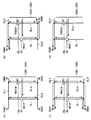
【図2】 メモリアレイおよびその周辺回路の実施の形態1に従う構成を説明する回路図である。
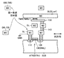
【図3】 メモリセルおよびリファレンスセル周辺の構造を示す断面図である。
【図4】 リファレンスセルを備えたMRAMデバイスにおけるデータ書込およびデータ読出動作を説明する第1の動作波形図である。
【図5】 リファレンスセルを備えたMRAMデバイスにおけるデータ書込およびデータ読出動作を説明する第2の動作波形図である。
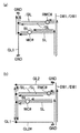
【図6】 実施の形態1に従う構成における接地配線の配置例を示す概念図である。
【図7】 メモリアレイおよびその周辺回路の実施の形態2に従う構成を説明する回路図である。
【図8】 実施の形態2に従うメモリセルおよびリファレンスセル周辺の構造を示す断面図である。
【図9】 実施の形態2に従う構成における接地配線の配置例を示す概念図である。
【図10】 メモリアレイおよびその周辺回路の実施の形態3に従う構成を説明する回路図である。
【図11】 実施の形態3に従うメモリセルおよびリファレンスセル周辺の構造例を示す断面図である。
【図12】 実施の形態3に従うメモリセルおよびリファレンスセル周辺の他の構造例を示す断面図である。
【図13】 実施の形態3に従う構成における接地配線の配置例を示す概念図である。
【図14】 メモリアレイおよびその周辺回路の実施の形態4に従う構成を説明する回路図である。
【図15】 実施の形態4に従う構成における接地配線の配置例を示す概念図である。
【図16】 MTJメモリセルの構成を示す概略図である。
【図17】 MTJメモリセルに対するデータ書込動作を説明する概念図である。
【図18】 データ書込時におけるデータ書込電流とトンネル磁気抵抗素子の磁化方向との関係を示す概念図である。
【図19】 MTJメモリセルからのデータ読出動作を説明する概念図である。
【符号の説明】
1 MRAMデバイス、10 メモリアレイ、20 行デコーダ、25 列デコーダ、70 センスアンプ、110 ソース領域(不純物領域)、120 ドレイン領域(不純物領域)、130 ゲート、ADD アドレス信号、ATR アクセストランジスタ、ATRr アクセス素子、BL,/BL ビット線、BLref リファレンスビット線、DB1,/DB1,DB2,/DB2 データバス、DIN 書込データ、DL ディジット線、DOUT 読出データ、DRWL0,DRWL1 ダミーリードワード線、FL 固定磁化層、GL,GL1,GL2 接地配線、GND 接地電圧、M1,M2,M3,M4 金属配線層、MC MTJメモリセル、MC♯ 選択メモリセル、RMC リファレンスセル、RMC♯ 選択リファレンスセル、RWL リードワード線、SL,/SL,SLd0,SLd1,SLr ソース線、TB トンネルバリア、TMR トンネル磁気抵抗素子、TMRr 基準抵抗、VL 自由磁化層、Vcc 電源電圧。[0001]
BACKGROUND OF THE INVENTION
The present invention relates to a storage device, and more particularly to a storage device including memory cells represented by a thin film magnetic storage device and having different electric resistance values depending on the data level of stored data.
[0002]
[Prior art]
MRAM devices are attracting attention as storage devices that can store nonvolatile data with low power consumption. An MRAM device is a storage device capable of performing random access using a plurality of thin film magnetic bodies formed in a semiconductor integrated circuit to perform nonvolatile data storage and each thin film magnetic body as a memory cell.
[0003]
In particular, in recent years, it has been announced that the performance of MRAM devices will be dramatically improved by using a thin film magnetic body using a magnetic tunnel junction as a memory cell. For MRAM devices with memory cells with magnetic tunnel junctions, see “A 10ns Read and Write Non-Volatile Memory Array Using a Magnetic Tunnel Junction and FET Switch in each Cell”, ISSCC Digest of Technical Papers, TA7.2, Feb 2000., “Nonvolatile RAM based on Magnetic Tunnel Junction Elements”, ISSCC Digest of Technical Papers, TA7.3, Feb. 2000., and “A 256kb 3.0V 1T1MTJ Nonvolatile Magnetoresistive RAM”, ISSCC Digest of Technical Papers, TA7. 6, Feb. 2001. and the like.
[0004]
FIG. 16 is a schematic diagram showing a configuration of a memory cell having a magnetic tunnel junction (hereinafter also simply referred to as “MTJ memory cell”).
[0005]
Referring to FIG. 16, the MTJ memory cell includes a tunnel magnetoresistive element TMR whose electric resistance changes according to the data level of magnetically written storage data, and an access transistor ATR. Access transistor ATR is connected in series with tunneling magneto-resistance element TMR between bit line BL and source line SL. Typically, a field effect transistor formed on a semiconductor substrate is applied as access transistor ATR.
[0006]
For MTJ memory cells, bit lines BL and digit lines DL for flowing data write currents in different directions at the time of data writing, word lines WL for instructing data reading, and tunnels at the time of data reading A source line SL for pulling down magnetoresistive element TMR to a fixed voltage (for example, ground voltage GND) is provided. At the time of data reading, tunnel magnetoresistive element TMR is electrically coupled between source line SL and bit line BL in response to turn-on of access transistor ATR.
[0007]
FIG. 17 is a conceptual diagram illustrating a data write operation for the MTJ memory cell.
[0008]
Referring to FIG. 17, tunneling magneto-resistance element TMR corresponds to a ferromagnetic layer (hereinafter also simply referred to as “fixed magnetization layer”) FL having a fixed fixed magnetization direction and an externally applied magnetic field. A ferromagnetic layer (hereinafter, also simply referred to as “free magnetic layer”) VL that is magnetized in the direction. A tunnel barrier (tunnel film) TB formed of an insulator film is provided between the fixed magnetic layer FL and the free magnetic layer VL. Free magnetic layer VL is magnetized in the same direction as fixed magnetic layer FL or in the opposite direction to fixed magnetic layer FL according to the level of stored data to be written. A magnetic tunnel junction is formed by these fixed magnetic layer FL, tunnel barrier TB and free magnetic layer VL.
[0009]
The electric resistance of tunneling magneto-resistance element TMR changes according to the relative relationship between the magnetization directions of fixed magnetic layer FL and free magnetic layer VL. Specifically, the electric resistance of tunneling magneto-resistance element TMR becomes the minimum value Rmin when the magnetization direction of fixed magnetic layer FL and the magnetization direction of free magnetic layer VL are the same (parallel), and the magnetization directions of both are The maximum value Rmax is obtained in the opposite (antiparallel) direction.
[0010]
At the time of data writing, word line WL is deactivated and access transistor ATR is turned off. In this state, the data write current for magnetizing free magnetic layer VL flows in the direction corresponding to the level of the write data in each of bit line BL and digit line DL.
[0011]
FIG. 18 is a conceptual diagram showing the relationship between the data write current and the magnetization direction of the tunnel magnetoresistive element at the time of data writing.
[0012]
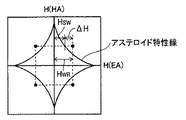
Referring to FIG. 18, the horizontal axis H (EA) represents a magnetic field applied in the easy axis (EA) direction in free magnetic layer VL in tunneling magneto-resistance element TMR. On the other hand, the vertical axis H (HA) indicates a magnetic field that acts in the hard magnetization axis (HA) direction in the free magnetic layer VL. Magnetic fields H (EA) and H (HA) respectively correspond to one of two magnetic fields generated by currents flowing through bit line BL and digit line DL, respectively.
[0013]
In the MTJ memory cell, the fixed magnetization direction of the fixed magnetization layer FL is along the easy magnetization axis of the free magnetization layer VL, and the free magnetization layer VL has the stored data level (“1” and “0”). Accordingly, it is magnetized in the direction parallel to the fixed magnetic layer FL or in the antiparallel (opposite) direction along the easy axis direction. The MTJ memory cell can store 1-bit data (“1” and “0”) corresponding to the two magnetization directions of the free magnetic layer VL.
[0014]
The magnetization direction of free magnetic layer VL can be rewritten only when the sum of applied magnetic fields H (EA) and H (HA) reaches a region outside the asteroid characteristic line shown in FIG. it can. That is, when the applied data write magnetic field has a strength corresponding to the region inside the asteroid characteristic line, the magnetization direction of the free magnetic layer VL does not change.
[0015]
As indicated by the asteroid characteristic line, by applying a magnetic field in the hard axis direction to the free magnetic layer VL, the magnetization threshold required to change the magnetization direction along the easy axis is lowered. be able to.
[0016]
When the operating point at the time of data writing is designed as in the example shown in FIG. 18, the strength of the data writing magnetic field in the easy axis direction in the MTJ memory cell that is the data writing target is H.WRDesigned to be That is, this data write magnetic field HWRIs designed so that the value of the data write current flowing through the bit line BL or the digit line DL is obtained. Generally, the data write magnetic field HWRIs a switching magnetic field H required for switching the magnetization direction.SWAnd the sum of the margin ΔH. That is, HWR= HSWIndicated by + ΔH.
[0017]
In order to rewrite the storage data of the MTJ memory cell, that is, the magnetization direction of the tunnel magnetoresistive element TMR, it is necessary to pass a data write current of a predetermined level or more to both the digit line DL and the bit line BL. Thus, free magnetic layer VL in tunneling magneto-resistance element TMR is parallel to fixed magnetic layer FL or in the opposite (anti-parallel) direction according to the direction of the data write magnetic field along the easy axis (EA). Magnetized. The magnetization direction once written in tunneling magneto-resistance element TMR, that is, data stored in the MTJ memory cell is held in a nonvolatile manner until new data writing is executed.
[0018]
FIG. 19 is a conceptual diagram illustrating a data read operation from the MTJ memory cell. Referring to FIG. 19, in the data read operation, access transistor ATR is turned on in response to activation of word line WL. Thereby, tunneling magneto-resistance element TMR is electrically coupled to bit line BL while being pulled down to predetermined voltage Vss.
[0019]
In this state, if the bit line BL is pulled up to a predetermined voltage, the current path including the bit line BL and the tunnel magnetoresistive element TMR is changed according to the electric resistance of the tunnel magnetoresistive element TMR, that is, the stored data of the MTJ memory cell. The memory cell current Icell according to the level passes. For example, the memory data can be read from the MTJ memory cell by comparing the memory cell current Icell with a predetermined reference current Iref (not shown).
[0020]
Thus, tunnel magnetoresistive element TMR changes its electrical resistance in accordance with the direction of magnetization that can be rewritten by the applied data write magnetic field, so that tunneling magnetoresistive element TMR has electrical resistances Rmax and Rmin, and stored data By associating with the levels (“1” and “0”), nonvolatile data storage can be executed.
[0021]
[Problems to be solved by the invention]
Thus, in the MRAM device, the tunnel magnetoresistive element TMR corresponding to the difference in the stored data level.InData storage is performed using the electrical resistance difference ΔR = (Rmax−Rmin), which is a junction resistance difference. That is, data reading is executed based on detection of a memory cell current passing through the selected memory cell.
[0022]
For data reading, a reference cell for generating a reference current to be compared with such a memory cell current is provided separately from a normal memory cell for executing data storage. That is, such a reference cell is designed to have an intermediate value between the two types of electrical resistances Rmax and Rmin of the MTJ memory cell.
[0023]
At the time of data reading, a current path of a memory cell current including a selected memory cell (hereinafter also referred to as “memory cell current path”) and a current path of a reference current including a reference cell (hereinafter also referred to as “reference current path”) And data reading is executed based on the comparison of the respective passing currents.
[0024]
Generally, the electric resistance of the tunnel magnetoresistive element is several tens of KΩ level, and a memory cell current of about 20 μA is generated by applying a low voltage of about 0.5 V across the tunnel magnetoresistive element at the time of data reading. appear. In this case, since the current difference caused by the electrical resistance difference ΔR is about several μA, detection of the electrical resistance difference between the selected memory cell and the reference cell requires a highly sensitive current comparison.
[0025]
Therefore, in these two current paths, if the electrical resistance of the path portion excluding the selected memory cell and the reference cell (hereinafter also referred to as “path resistance”) is greatly different, the electrical resistance difference between the selected memory cell and the reference cell is accurately determined. Data cannot be read well, and the data reading accuracy is lowered.
[0026]
In general, in an MRAM device, MTJ memory cells are integrated and arranged in a matrix, so that at least the memory cell current path changes depending on the position of the selected memory cell indicated by the address selection result. Therefore, depending on the address selection result, it is necessary to consider that the difference in path resistance does not change between the memory cell current path and the reference current path. Such a problem is common not only to MRAM devices but also to storage devices having memory cells whose electrical resistance values change according to the level of stored data.
[0027]
The present invention has been made to solve such a problem, and an object of the present invention is to provide a data storage device for reading data based on a difference in electrical resistance between a reference cell and a selected memory cell. The purpose is to improve the read margin.
[0028]
[Means for Solving the Problems]
A memory device according to the present invention includes a plurality of memory cells each having one of two levels of electrical resistance in accordance with stored data,Provided as a comparison target of a selected memory cell at the time of data reading among a plurality of memory cellsA memory array having a plurality of reference cells arranged in a matrix is provided. The plurality of reference cells are arranged along one of the rows and columns so as to share the other of the rows and columns with the plurality of memory cells. The storage device is arranged corresponding to each row, and corresponds to each of a plurality of word lines activated in the selected row, a plurality of data lines arranged corresponding to each column, and one of the row and the column. A plurality of source lines each supplying a fixed voltage.furtherPrepare. Each of the plurality of memory cells includes a storage element connected in series between a corresponding one of the plurality of data lines and a corresponding one of the plurality of source lines, and an electric resistance that changes according to stored data Access element turned on in response to activation of corresponding word lineChildThe plurality of data lines include a first data line connected to a selected memory cell selected as a data reading target among a plurality of memory cells at the time of data reading, and a plurality of reference cells at the time of data reading. And a second data line connected to the selected reference cell sharing the other of the row and column with the selected memory cell. The memory device couples the first and second data lines with a voltage different from the fixed voltage during data reading to form first and second current paths that pass through the selected memory cell and the selected reference cell, respectively. A circuit is further provided, and the data read circuit reads stored data from the selected memory cell based on a difference in electrical resistance between the first and second current paths.
[0029]
Preferably, the electrical resistance per unit length of the plurality of data lines is the plurality of sources.lineIs less than the electrical resistance per unit length.
[0030]
More preferably, the plurality of data lines are formed by metal wiring, and the plurality of source lines are formed by an impurity diffusion layer provided on the semiconductor substrate so as to extend in one of the row and the column.
[0031]
Preferably, the storage device further includes a fixed voltage wiring arranged along the other of the row and the column in a region adjacent to the memory array, and each of the plurality of source lines has a fixed voltage.ArrangementElectrically coupled to the wire.
[0032]
Or preferably a fixed voltageArrangementMultiple sources of electrical resistance per unit length of wirelineIs less than the electrical resistance per unit length.
[0033]
More preferably, the storage device further includes first and second data buses arranged along the row in a region adjacent to the memory array. At the time of data reading, the first and second data lines are electrically connected to the data reading circuit via the first and second data buses, and the electric resistance per unit length of the fixed voltage wiring is a plurality of One of the data line and the data bus is designed to be equivalent to the electric resistance per unit length arranged in the same direction as the fixed voltage wiring.
[0034]
A memory device according to another configuration of the present invention includes a plurality of memory cells each having one of two levels of electrical resistance in accordance with stored data,Provided as a comparison target of a selected memory cell at the time of data reading among a plurality of memory cellsThe memory array includes a plurality of reference cells arranged in a matrix, and the plurality of reference cells are arranged along a row so as to share a column with the plurality of memory cells. The storage device is arranged corresponding to each row, and is arranged corresponding to each of a plurality of word lines activated in a selected row, a plurality of data lines arranged corresponding to each column, and a column, A plurality of source lines each supplying a fixed voltagefurtherPrepare. Each of the plurality of memory cells includes a storage element connected in series between a corresponding one of the plurality of data lines and a corresponding one of the plurality of source lines, and an electric resistance that changes according to stored data And an access element that is turned on in response to activation of the corresponding word line, and the plurality of data lines are connected to a selected memory cell selected as a data read target among the plurality of memory cells at the time of data reading. A first data line and a second data line connected to a selected reference cell sharing a column with a selected memory cell among a plurality of reference cells at the time of data reading. The memory device couples the first and second data lines with a voltage different from the fixed voltage during data reading to form first and second current paths that pass through the selected memory cell and the selected reference cell, respectively. And a data read circuit for reading stored data from the selected memory cell based on a difference in electric resistance between the first and second current paths, wherein the electric resistance per unit length of the plurality of data lines includes a plurality of electric resistances. Designed to be equivalent to the electrical resistance per unit length of the source line.
[0035]
A memory device according to still another configuration of the present invention includes a plurality of memory cells each having one of two levels of electrical resistance according to stored data,Provided as a comparison target of a selected memory cell at the time of data reading among a plurality of memory cellsThe memory array includes a plurality of reference cells arranged in a matrix, and the plurality of reference cells are arranged along a column so as to share a row with the plurality of memory cells. The storage device is arranged corresponding to each row, and is arranged corresponding to each of a plurality of word lines activated in the selected row, a plurality of data lines arranged corresponding to each of the columns, and a row, A plurality of source lines each supplying a fixed voltagefurtherPrepare. Each of the plurality of memory cells includes a storage element connected in series between a corresponding one of the plurality of data lines and a corresponding one of the plurality of source lines, and an electric resistance that changes according to stored data And an access element that is turned on in response to activation of the corresponding word line, and the plurality of data lines are connected to a selected memory cell selected as a data read target among the plurality of memory cells at the time of data reading. And a second data line connected to a selected reference cell sharing a row with a selected memory cell among a plurality of reference cells at the time of data reading. The memory device is arranged along a row in a region adjacent to the memory array, and is electrically connected to the first and second data lines at the time of data reading, and the first and second data buses at the time of data reading. A data read circuit is further provided for coupling the first and second data buses with a voltage different from the fixed voltage to form first and second current paths passing through the selected memory cell and the selected reference cell, respectively. The data read circuit reads stored data from the selected memory cell based on the difference in electrical resistance between the first and second current paths, and the electrical resistance per unit length of the plurality of source lines is the first and second data. Designed to be equivalent to electrical resistance per unit length of wire.
[0036]
Preferably, at the time of data reading, the electric resistance of the portion excluding the selected memory cell from the first current path is balanced with the electric resistance of the portion excluding the selected reference cell from the second current path.
[0037]
Preferably, the memory element has a plurality of magnetic films, and at least one of the plurality of magnetic films is magnetized in a direction corresponding to the stored data.
[0038]
Alternatively, preferably, at the time of data reading, the first and second data lines are coupled with a common voltage different from the fixed voltage, and the data reading circuit is based on a difference in passing current between the first and second data lines, Read stored data from the selected memory cell.
[0039]
Preferably, at the time of data reading, the first and second data lines are supplied with the same current, and the data reading circuit stores data from the selected memory cell based on the voltage difference between the first and second data lines. Read data.
[0040]
DETAILED DESCRIPTION OF THE INVENTION
Hereinafter, embodiments of the present invention will be described in detail with reference to the drawings. In addition, the same code | symbol in a figure shall show the same or an equivalent part.
[0041]
[Embodiment 1]
FIG. 1 is a schematic block diagram showing an overall configuration of
[0042]
The
[0043]
Referring to FIG. 1,
[0044]
The
[0045]
In
[0046]
The
[0047]
Read /
[0048]
Digit line DL is coupled to a predetermined voltage Vss (for example, ground voltage) in a region opposite to row
[0049]
FIG. 2 is a circuit diagram illustrating a configuration according to the first embodiment of the memory array and its peripheral circuits.
[0050]
Referring to FIG. 2,
[0051]
Read word lines RWL1 to RWLn, digit lines DL1 to DLn, and source lines SL1 to SLn are arranged corresponding to the memory cell rows, respectively. Complementary bit lines BL1, / BL1 to BLm, / BLm are provided corresponding to the memory cell columns, respectively.
[0052]
Each of source lines SL1 to SLn is connected at both ends to ground lines GL1 and GL2, and supplies ground voltage GND to memory cell MC. In the following, the read word lines RWL1 to RWLn, the digit lines DL1 to DLn, the bit lines BL1 to BLm, / BL1 to / BLm and the source lines SL1 to SLn are collectively referred to as the read word line RWL, the digit line DL, Also referred to as bit lines BL, / BL and source line SL. The binary high voltage state (for example, power supply voltage Vcc) and low voltage state (for example, ground voltage GND) of the signal, signal line, and data are also referred to as “H level” and “L level”, respectively.
[0053]
Each memory cell MC is configured in the same manner as shown in FIG. 16, and includes tunneling magneto-resistance element TMR and access transistor ATR connected in series between corresponding bit line BL or / BL and source line SL. . Access transistor ATR has its gate connected to corresponding read word line RWL. Tunneling magneto-resistance element TMR is magnetized in a direction corresponding to stored data (“1” or “0”) and has one of electric resistances Rmax and Rmin. It should be noted that the portion corresponding to tunneling magneto-resistance element TMR can be replaced with another element whose electric resistance changes according to the level of stored data.
[0054]
Strictly speaking, the electric resistance of each memory cell is the sum of the tunnel magnetoresistive element TMR, the on-resistance of the access transistor ATR, and other parasitic resistances. The resistance other than the tunnel magnetoresistive element TMR depends on the stored data. In the following, the electric resistances of the two types of normal memory cells corresponding to the stored data are also represented by Rmax and Rmin, and the difference between them is represented by ΔR (that is, ΔR = Rmax−Rmin). And
[0055]
Memory cell MC is coupled to one of bit lines BL1-BLm and / BL1- / BLm for each row. Memory cells MC belonging to odd rows (for example, first row) are coupled to bit lines BL1 to BLm, and memory cells MC belonging to even rows (for example, second row) are connected to bit lines / BL1 to / BLm. .
[0056]
The
[0057]
Each reference cell RMC has a reference resistor TMRr and an access element ATRr connected in series between the corresponding bit line BL or / BL and the corresponding source line SLd. Access element ATRr is formed of a field effect transistor similarly to access transistor ATR in the MTJ memory cell, and its gate is connected to a corresponding one of dummy read word lines DRWL0 and DRWL1.
[0058]
The electrical resistance of the reference cell RMC is designed to be an intermediate level between the two types of electrical resistances Rmax and Rmin of each memory cell MC, preferably (Rmax + Rmin) / 2. For example, the reference resistor TMRr is designed in the same manner as the tunnel magnetoresistive element TMR in the MTJ memory cell MC, and the storage data corresponding to the electric resistance Rmin is written in advance, and the size of the transistor constituting the access element ATRr is A reference cell having such characteristics is realized by making it different from the access transistor ATR or setting the gate voltage of the access element ATRr, that is, the H level voltage of the dummy read word line DRWL to a level different from that of the read word line RWL. Is done.
[0059]
Since it is not necessary to rewrite the data stored in the reference cell RMC, it is not necessary to arrange the digit lines DLd0 and DLd1 provided corresponding to the reference cell rows shown in FIG. By providing the line, the continuity of the shape pattern at the end of the
[0060]
Reference cell RMC is selected by one of dummy read word lines DRWL0 and DRWL1. In the reference cell group selected by the dummy read word line DRWL0, the access element ATRr is turned on in response to the activation of the dummy read word line DRWL0. The dummy read word line DRWL0 is activated together with the read word line RWL of the selected row when the even row includes the selected memory cell. Therefore, when an even-numbered row is selected, tunnel magnetoresistive element TMR is electrically coupled between bit lines / BL1 to / BLm and source line SL, respectively, while bit lines BL1 to BLm and source line SLd0 are connected to each other. A reference resistor TMRr is electrically coupled between them.
[0061]
On the other hand, in the remaining reference cell group selected by dummy read word line DRWL1, access element ATRr is turned on in response to activation of dummy read word line DRWL1. The dummy read word line DRWL1 is activated together with the read word line RWL of the selected row when the odd row includes the selected memory cell. Therefore, when an odd row is selected, tunnel magnetoresistive element TMR is electrically coupled between bit lines BL1 to BLm and source line SL, respectively, while bit lines / BL1 to / BLm and source line SLd1 are connected to each other. A reference resistor TMRr is electrically coupled between them.
[0062]
FIG. 3 is a cross-sectional view showing the structure around the memory cell MC and the reference cell RMC.
[0063]
Referring to FIG. 3, access transistor ATR (or access element ATRr) formed on semiconductor substrate SUB has
[0064]
[0065]
The
[0066]
The read word line RWL is generally provided as a polysilicon wiring provided extending in the row direction. By the polysilicon wiring,
[0067]
As described above, the digit line DL and the bit line BL through which the data write current flows form a metal wiring having a relatively small electric resistance, while the source line SL and the read word line RWL that do not need to pass the data write current are formed. By forming without using metal wiring, the number of metal wiring layers required for the configuration of the memory cell MC and the reference cell RMC can be reduced, and the cell can be miniaturized. As a result, the size of the device can be reduced by reducing the area of the memory array.
[0068]
Next, the configuration around the
Referring to FIG. 2 again,
[0069]
As a result, digit line DL of the selected row is connected to power supply voltage Vcc and ground voltage GND at one end and the other end in response to turn-on of
[0070]
In an area adjacent to
[0071]
Further, column select lines CSL1 to CSLm and column select gates CSG1, / CSG1 to CSGm, / CSGm are provided corresponding to each of the memory cell columns, and a precharge transistor is provided corresponding to each of bit lines BL and / BL. 67 is provided.
[0072]
The
[0073]
Column select gates CSG1, / CSG1 to CSGm, / CSGm are provided in a region corresponding to read /
[0074]
Similarly, column selection gates / CSG1- / CSGm are arranged between bit lines / BL1- / BLm and data bus / DB1, respectively. Each of column select gates / CSG1- / CSGm responds to activation of a corresponding one of column select lines CSL1-CSLm.TheThe data bus / DB1 and the corresponding bit line / BL are connected.
[0075]
[0076]
The precharge signal φPR is activated to precharge the bit lines BL and / BL before and after the data write operation and data read operation within the standby period of the
[0077]
Bit line drivers BDVa1 to BDVam and BDVb1 to BDVbm are provided corresponding to both ends of the bit lines BL1 to BLm, respectively. Bit line drivers BDVa1 to BDVam belong to read /
[0078]
The bit line driver BDVa1 is connected between the
[0079]
[0080]
In contrast, the bit line driver BDVb1 includes a
[0081]
The
[0082]
Further, bit line drivers / BDVa1 to / BDVam and / BDVb1 to / BDVbm are provided corresponding to both ends of the bit lines / BL1 to / BLm, respectively. Bit line drivers / BDVa1 to / BDVam belong to read /
[0083]
Bit line driver / BDVa differs from bit line driver BDVa only in that one of the inputs to the logic gate is not data bus DB1, but data bus / DB1. Similarly, bit line driver / BDVb differs from bit line driver BDVb only in that one of the inputs to the logic gate is not data bus DB2, but data bus / DB2.
[0084]
At the time of data writing, data buses DB1 and / DB1 are driven to one of different voltages (for example, power supply voltage Vcc and ground voltage GND) according to write data DIN by a data write circuit (not shown). The voltages on data buses DB2 and / DB2 are similarly driven to complementary levels. Data buses DB1 and DB2 are driven to the same voltage, and / DB1 and / DB2 are also driven to the same voltage.
[0085]
For example, when write data is "1", data buses DB1 and DB2 are driven to power supply voltage Vcc (H level), and data buses / DB1 and / DB2 are driven to ground voltage GND (L level). In contrast, when the write data is "0", data buses / DB1 and / DB2 are driven to power supply voltage Vcc (H level), and data buses DB1 and DB2 are driven to ground voltage GND (L level). The
[0086]
With such a configuration, currents in opposite directions flow through bit lines BL and / BL in the selected column during data writing. The direction of these currents is controlled according to the voltage levels of data buses DB1, DB2 and / DB1, / DB2, that is, the level of write data DIN.
[0087]
Specifically, when H level data is written (DIN = “1”), a data write current is supplied to the bit line BL of the selected column in the direction from the bit line driver BDVa to BDVb. A data write current is supplied to line / BL in the direction from bit line driver / BDVb to / BDVa. In contrast, when L level data is written (DIN = “0”), data write currents are applied to bit lines BL and / BL of the selected column in opposite directions to those at the time of writing H level data. Will be washed away. A data write magnetic field along the easy axis (EA) direction acts on the corresponding memory cell by the data write current in the direction corresponding to the write data DIN.
[0088]
As a result, the selected memory cell is easily magnetized in the direction according to the magnetic field along the hard axis from the digit line DL of the selected row and the write data DIN from the bit lines BL and / BL of the selected column. Since both the magnetic field along the axis acts, the tunnel magnetoresistive element TMR is magnetized in the direction corresponding to the level of the write data DIN in the selected memory cell.
[0089]
At the time of data reading, read word line RWL in the selected row and column select line CSL in the selected column are activated. In FIG. 2, as an example, it is assumed that read word line RWL2 and column selection line CSL1 are activated. Since the read word line RWL2 of the even-numbered row is activated, the dummy read word line DRWL0 is activated correspondingly, and DRWL1 is deactivated. As a result, selected memory cell MC # is connected between bit line / BL1 and source line SL2, and the selected reference cell (hereinafter also referred to as “selected reference cell”) is connected to bit line BL1 and source line SLd0. Connected between.
[0090]
In response to activation of column select line CSL1, bit lines BL1 and / BL1 corresponding to the selected column are sense amplifiers (data for reading stored data from the selected memory cells via data buses DB1 and / DB1). Read circuit 70).
[0091]
The data writing and data reading operations in the
[0092]
Referring to FIG. 4, the data write operation waveform for selected memory cell MC # is shown at the time of data write.
[0093]
At the time of data writing, each read word line RWL and dummy read word line DRWL are inactivated to L level (ground voltage GND), and digit line DL in the selected row and column select line CSL in the selected column are activated. (Not shown).
[0094]
As a result, the data write current Ip in a fixed direction and the data write current ± Iw in the direction corresponding to the write data are supplied to the digit line DL of the selected row and the bit lines BL and / BL of the selected column, respectively. . As a result, data writing is performed on selected memory cell MC # located at the intersection of the digit line of the selected row and the bit line of the selected column. As already described, data writing to the reference cell RMC is not necessary during actual operation.
[0095]
At the time of data reading, read word line RWL corresponding to the selected row and corresponding dummy read word line DRWL are activated to H level. On the other hand, each digit line DL is deactivated and no current flows. Although not shown, the column selection line CSL of the selected column is activated.
[0096]
The H level voltage of read word line RWL and dummy read word line DRWL is set according to the configuration of the reference cell. For example, when the reference resistor TMRr is formed with an intermediate resistance between the electric resistances Rmax and Rmin, the H level voltage of the read word line RWL and the dummy read word line DRWL may be the same level (VDWL = Vcc). . On the other hand, when reference resistance TMRr is designed in the same manner as tunneling magneto-resistance element TMR and magnetized in the direction corresponding to electric resistance Rmin, the on-resistance of access element ATRr is larger than the on-resistance of access transistor ATR. Therefore, the H level voltage VDWL of the dummy read word line DRWL is set lower than the H level voltage (Vcc) of the read word line RWL.
[0097]
As already described, for example, when data is read when an even-numbered row is selected, data buses DB1 and / DB1 are pulled down to ground voltage GND via selected memory cell MC # and selected reference cell RMC #, respectively.
[0098]
At this time, one of two levels corresponding to the stored data flows as memory cell current Icell to one of bit lines BL and / BL of the selected column connected to selected memory cell MC #. On the other hand, a reference current Iref having an intermediate level between the two kinds of levels flows through the other of the bit lines BL and / BL of the selected column connected to the selected reference cell RMC #. Therefore,
[0099]
FIG. 5 shows a variation of the data read operation. In the data read operation shown in FIG. 5,
[0100]
Therefore,
[0101]
4 and 5, the
[0102]
Next, a configuration for balancing the path resistances of the memory cell current path and the reference current path during data reading will be described.
[0103]
Referring again to FIG. 2, at the time of data reading, the memory cell current is derived from
[0104]
As described in FIG. 3, these source lines SL2 and SLd0 are formed by a diffusion layer having a relatively high electrical resistance. Therefore, the path resistance obtained by removing selected memory cell MC # and selected reference cell RMC # from these current paths changes according to the current path length on source lines SL (SL2) and SLd. In particular, if the current path lengths on the source lines SL (SL2) and SLd are greatly different between the memory cell current path and the reference current path, a large difference is caused in the path resistance between these current paths, and data reading is performed. The margin is lowered.
[0105]
In the configuration in which the reference cell row is provided, the selected memory cell MC # and the selected reference cell RMC # belong to the same memory cell column, and therefore on the wiring along the row direction between the memory cell current path and the reference current path. Are naturally balanced regardless of the column selection result.
[0106]
Therefore, in the configuration according to the first embodiment, by matching the arrangement directions of source lines SL and SLd and the reference cell, the path resistances of the memory cell current path and the reference current path are balanced regardless of the column selection result. ing. That is, by arranging the source lines SL and SLd along the row direction, the path lengths on the source lines SL and SLd having high electrical resistance between the memory cell current path and the reference current path are affected by the column selection result. Can be balanced.
[0107]
As a result, the difference in total electrical resistance between the memory cell current path and the reference current path clearly reflects the electrical resistance difference between the selected memory cell MC # and the selected reference cell RMC #, and therefore depends on the address selection result. Thus, it is possible to prevent a decrease in the data read margin.
[0108]
In the configuration in which the reference cell row is provided, the path length on the wiring along the column direction between the memory cell current path and the reference current path is:lineIt changes depending on the selection result. However, since bit lines BL, / BL and ground wirings GL1, GL2 provided along the column direction are each formed of a low-resistance metal wiring, such a path length difference affects the data read margin. It is unlikely that such a path resistance difference will occur.
[0109]
Alternatively, as a more desirable configuration, if each of the bit line BL and the ground wirings GL1 and GL2 provided along the column direction is designed so that the electric resistance per unit length is equal, the memory cell current path and the reference current path The data read margin can be further improved by suppressing the path resistance difference depending on the row selection result between the two. In order to equalize the electrical resistance per unit length, for example, each of the bit line BL and the ground wirings GL1, GL2 may be formed of the same shape and the same material.
[0110]
Further, as shown in FIG. 2, the memory cell current path and the reference current path can be made symmetrical by coupling one end of each of the ground lines GL1 and GL2 to the ground voltage GND so as to be symmetrical. As a result, the data read operation can be further stabilized.
[0111]
FIG. 6 shows an arrangement arrangement for ground wirings GL1 and GL2.
[0112]
Referring to FIG. 6 (a), both ends of ground lines GL1 and GL2 may be connected to ground voltage GND. Even with such a configuration, the path resistance can be balanced between the memory cell current path and the reference current path regardless of the address selection result.
[0113]
FIG. 6B shows a configuration similar to that shown in FIG. 2, that is, a configuration in which one ends of the ground wirings GL1 and GL2 are symmetrically connected to the ground voltage GND.
[0114]
Alternatively, as shown in FIG. 6C, even if the same side of both ends of the ground lines GL1 and GL2 is connected to the ground voltage GND, the ground lines GL1 and GL2ofAlthough the current path length differs between the memory cell current path and the reference current path, since the current path lengths on the source lines SL and SLd having a large electric resistance are balanced, the data read margin is not greatly reduced. Absent.
[0115]
Therefore, if the arrangement direction of the reference cell RMC and the arrangement direction of the source lines SL and SLd are matched, only the ground wiring GL1 is arranged on one side of the
[0116]
[Embodiment 2]
FIG. 7 is a circuit diagram illustrating a configuration according to the second embodiment of the memory array and its peripheral circuits.
[0117]
Referring to FIG. 7, in the configuration according to the second embodiment, as compared with the configuration according to the first embodiment, a plurality of reference cells RMC are arranged along the column direction so as to form a reference cell column. Is different. The plurality of reference cells RMC are arranged so as to share the memory cell rows with the plurality of memory cells MC, respectively.
[0118]
As a result, the bit lines BL1 to BLm are connected only to the memory cell MC. On the other hand, a reference bit line BLref is arranged corresponding to the reference cell column, and each reference cell RMC is connected between the corresponding one of the reference bit line BLref and the source lines SL1 to SLn.
[0119]
As already described, since it is not necessary to rewrite the data stored in the reference cell RMC, data writing to the reference cell RMC is not necessary. Therefore, it is not necessary to place bit line drivers at both ends of the reference bit line BLref. However, in the configuration according to FIG. 8, bit line drivers BDVar and BDVbr are arranged as shape dummies. In other words, bit line drivers BDVar and BDVbr are not actually used for data write operation, but the arrangement of the shape dummies ensures the continuity of the shape in the bit line driver arrangement region, and the memory array It is possible to reduce the variation in the finished size and shape of the 10 peripheral portions.
[0120]
Source line SL is arranged along the row direction as in the configuration shown in FIG. 2, and at least one of both ends thereof is coupled to ground voltage GND by a ground wiring. In the example shown in FIG. 7, one end side of each source line (opposite side of the sense amplifier 70) is connected to the ground wiring GL1 arranged along the column direction.
[0121]
Bit lines BL1 to BLm are connected to data bus DB1 via column selection gates CSG1 to CSGm, respectively, and reference bit line BLref is connected to data bus / DB1 via column selection gate CSGr. Column select gate CSGr is turned on in response to activation of column select line CSLr.
[0122]
In the configuration according to FIG. 7, column select lines CSL1-CSLm are selectively activated according to the column selection result at each of data reading and data writing. On the other hand, column selection line CSLr is activated at the time of data reading and inactivated at the time of data writing regardless of the column selection result.
[0123]
Since the configuration of other parts in FIG. 7 is the same as that shown in FIG. 2, detailed description will not be repeated. The data write operation is executed in the same manner as in the configuration of FIG. 2 using
[0124]
Next, a data read operation in the configuration according to the second embodiment will be described.
In FIG. 7, as in FIG. 2, read word line RWL2 and column select line CSL1 are activated to H level, and the memory cells in the second row and first column are selected and selected as selected memory cells MC #. A reference cell sharing the same memory cell row as memory cell MC # is selected as selected reference cell RMC #.
[0125]
At the time of data reading, a memory cell current is a memory cell current path composed of a
[0126]
In the configuration in which the reference cell column is provided, the selected memory cell MC # and the selected reference cell RMC # belong to the same memory cell row, and therefore, on the wiring along the column direction between the memory cell current path and the reference current path. , That is, the path length on the bit line BL and the reference bit line BLref, and the path length on the ground wiring GL1 are naturally balanced regardless of the column selection result. On the other hand, the path length on the wiring along the row direction differs between the memory cell current path and the reference current path.
[0127]
Therefore, in the configuration in which the arrangement direction of the reference cell and the arrangement direction of the source line SL do not match as in the second embodiment, the current path on the source line SL is between the memory cell current path and the reference current path. Therefore, the electrical resistance per unit length is the same between the source line SL and each of the data buses DB1, DB1 arranged in parallel to the source line and included in the memory cell current and the reference current path. It is necessary to design so that
[0128]
FIG. 8 is a cross sectional view showing the structure around the memory cell and the reference cell according to the second embodiment.
[0129]
Referring to FIG. 8, the configuration according to the second embodiment is different from the configuration according to the first embodiment shown in FIG. 3 in that source line SL is arranged as a metal wiring. That is, in the configuration according to the second embodiment, one more metal wiring layer is required as compared with the configuration shown in FIG. 3. For example, source lines SL and digit lines DL are provided in metal
[0130]
Source line SL, which is a metal wiring provided along the row direction, is electrically coupled to each
[0131]
Further, in the region adjacent to the
[0132]
By adopting such a configuration, even in a configuration in which the arrangement direction of the source line SL and the reference cell RMC does not match, the path resistance of the memory cell current path and the reference current path can be balanced regardless of the address selection result. it can. As a result, the difference in total electrical resistance between the memory cell current path and the reference current path clearly reflects the electrical resistance difference between the selected memory cell MC # and the selected reference cell RMC #. Therefore, it is possible to prevent the data read margin from being lowered depending on the address selection result and to stabilize the data read operation.
[0133]
FIG. 9 shows variations of the arrangement of ground wirings arranged in adjacent areas of the
[0134]
Alternatively, as shown in FIG. 9B, both ends of the ground wiring GL1 may be connected to the ground voltage GND. According to the configuration of FIG. 9B, the current path length on the ground wiring GL1 that changes according to the row selection result can be shortened on average, so that the total resistance value of the current path of the data read current is substantially reduced. Therefore, it is possible to reduce power consumption.
[0135]
[Embodiment 3]
In the third embodiment, a configuration in which the source line SL is also arranged along the column direction with respect to the reference cell RMC arranged along the column direction will be described.
[0136]
FIG. 10 is a circuit diagram illustrating a configuration according to the third embodiment of the memory array and its peripheral circuits.
[0137]
Referring to FIG. 10, in the configuration according to the third embodiment, column lines are replaced with source lines SL1 to SLn arranged along the row direction as compared with the configuration according to the second embodiment shown in FIG. The difference is that source lines SL1 to SLm, SLr arranged along the direction are arranged. The source lines SL1 to SLm are also simply referred to as source lines SL when collectively referred to. The source line SLr is provided corresponding to the reference cell column, and each of the plurality of reference cells RMC is connected between the reference bit line BLref and the source line SLr.
[0138]
Source lines SL and SLr are arranged along the column direction, and at least one of both ends thereof is coupled to ground voltage GND by a ground wiring. FIG.0In the example shown in FIG. 5, one end side of each source line SL and SLr (opposite side of the sense amplifier 70) is connected to the ground wiring GL1 arranged along the row direction. Both ends of the ground wiring GL1 are coupled to the ground voltage GND.
[0139]
Since the structure of the other part of FIG. 10 is the same as that shown in FIG. 7, detailed description will not be repeated. The data write operation is executed in the same manner as in the configuration of FIG. 2 using
[0140]
Next, a data read operation in the configuration according to the second embodiment will be described.
Also in FIG. 10, as in FIG. 2, read word line RWL2 and column select line CSL1 are activated to the H level, and the memory cells in the second row and the first column are selected and selected as the selected memory cell MC #. It is assumed that a reference cell sharing the same memory cell row as memory cell MC # is selected as selected reference cell RMC #.
[0141]
At the time of data reading, the memory cell current is a memory cell current path composed of a path of
[0142]
As already described, in the configuration in which the reference cell column is provided, the path length on the wiring along the column direction is naturally balanced between the memory cell current path and the reference current path regardless of the row selection result. To do. Therefore, in the configuration according to the third embodiment, by arranging source lines SL and SLr along the column direction, the path lengths on source lines SL and SLr in the memory cell current path and the reference current path, respectively, are changed. It can be balanced regardless of the selection result.
[0143]
As a result, similar to the configuration shown in FIG. 2, the source line SL can be realized even if the source line SL is formed as a diffusion layer formed extending in the column direction without providing a new metal wiring layer.
[0144]
FIG. 11 is a cross-sectional view showing a structural example around the memory cell and the reference cell according to the third embodiment. FIG. 11 shows a structural example of an MTJ memory cell having a source line SL provided as a diffusion layer.
[0145]
Referring to FIG. 11, in the configuration according to the third embodiment, source line SL (or SLr) is connected between access transistors ATR (or access elements ATRr) of memory cells MC (or reference cells RMC) adjacent in the column direction. And have
[0146]
That is, the
[0147]
Similarly to the structure shown in FIG. 3, drain
[0148]
Alternatively, as shown in FIG. 12, the source line SL can be provided as a metal wiring.
[0149]
Referring to FIG. 12, in such a structural example,
[0150]
According to the structure example of FIG. 12, although the number of necessary metal wiring layers is increased, the resistance of the source line SL can be reduced, so that the total electric resistance of the memory cell current path and the reference current path is suppressed. Is possible.
[0151]
As described above, regardless of which of the structures shown in FIGS. 12 and 13 is applied to the memory cell MC and the reference cell RMC, the path resistances of the memory cell current path and the reference current path are used as the address selection result. Regardless, the data read margin can be secured by balancing.
[0152]
In the configuration in which the reference cell column is provided, the path length on the wiring along the row direction changes between the memory cell current path and the reference current path depending on the column selection result. However, since the data buses DB1, / DB1 and the ground wiring GL1 provided along the row direction are each formed of a metal wiring of a low resistance material, such a path length difference affects the data reading margin. It is unlikely that a difference in path resistance will occur.
[0153]
Alternatively, as a more desirable configuration, if the data buses DB1, / DB1 and the ground wiring GL1 provided along the row direction are designed so that the electrical resistance per unit length is equal, the memory cell current path and the reference current path BetweenColumnThe data read margin can be further improved by suppressing the path resistance difference depending on the selection result. In order to equalize the electrical resistance per unit length, for example, the data buses DB1, / DB1 and the ground wiring GL1 may be formed of the same shape and the same material.
[0154]
FIG. 13 shows an arrangement arrangement for ground wirings GL1 and GL2. FIG. 13A shows a configuration in which the ground wiring GL1 provided along the row direction is connected to the ground voltage GND at a node opposite to the
[0155]
Therefore, as described above, if the ground wiring GL and the data buses DB1 and / DB1 are designed so that the electrical resistance per unit length is equal, the data read accuracy can be further improved.
[0156]
Alternatively, as shown in FIG. 9B, a ground wiring GL2 along the column direction can be further provided in an adjacent region of the
[0157]
[Embodiment 4]
In the fourth embodiment, as in the first embodiment, a configuration in which the source line SL is arranged in the column direction in the configuration in which the reference cells are arranged in the row direction will be described.
[0158]
FIG. 14 is a circuit diagram illustrating a configuration according to the fourth embodiment of the memory array and its peripheral circuits.
[0159]
Referring to FIG. 14, in the configuration according to the fourth embodiment, source lines SL1 to SLn, SLd0, and SLd1 arranged along the row direction are compared with the configuration according to the first embodiment shown in FIG. Instead, source lines SL1, / SL1,..., / SLm arranged along the column direction are different. Note that when the source lines SL1 to SLm are collectively referred to, they are simply expressed as the source line SL, and when the source lines / SL1 to / SLm are collectively referred to, they are simply expressed as the source line / SL.
[0160]
Source lines SL and / SL are arranged along the column direction, and at least one of both ends thereof is coupled to ground voltage GND by a ground wiring. In the example shown in FIG. 14, one end side (opposite side of the sense amplifier 70) of each source line is connected to the ground wiring GL1 arranged along the row direction. Both ends of the ground wiring GL1 are coupled to the ground voltage GND.
[0161]
In each memory cell column, the memory cell MC and the reference cell RMC are connected between one of the bit lines BL and / BL and one of the source lines SL and / SL.
[0162]
The configuration of other parts in FIG. 14 is the same as that shown in FIG. 2, and therefore detailed description will not be repeated. The data write operation is executed in the same manner as in the configuration of FIG. 2 using
[0163]
Next, a data read operation in the configuration according to the fourth embodiment will be described.
In FIG. 14, as in FIG. 2, read word line RWL2 and column select line CSL1 are activated to H level, and the memory cells in the second row and first column are selected and selected as selected memory cells MC #. A reference cell sharing the same memory cell column as memory cell MC # is selected as selected reference cell RMC #.
[0164]
At the time of data reading, the memory cell current is a memory cell current path comprising
[0165]
In the configuration in which the reference cell row is provided, the selected memory cell MC # and the selected reference cell RMC # belong to the same memory cell column, and therefore on the wiring along the row direction between the memory cell current path and the reference current path. The path lengths on the data buses DB1, / DB1 and the ground wiring GL1 are naturally balanced regardless of the row selection result. On the other hand, the path length on the wiring along the column direction differs between the memory cell current path and the reference current path.
[0166]
Therefore, in the configuration in which the arrangement direction of the reference cells and the arrangement direction of the source lines SL do not match as in the fourth embodiment, the source lines SL and / SL are placed between the memory cell current path and the reference current path. The current path length of inevitably differs. For this reason, each of the source lines SL, / SL and the data buses DB1, / DB1 arranged in parallel to the source lines SL, / SL and included in the memory cell current and the reference current path is connected to the electric resistance per unit length. Must be designed to be similar. In other words, the memory cell MC and the reference cell RMC have the structure shown in FIG.2The source line SL needs to be formed of a metal wiring by applying the structure shown in FIG.
[0167]
With such a configuration, the path resistances of the memory cell current path and the reference current path can be balanced regardless of the address selection result even in a configuration in which the arrangement direction of the source line SL and the reference cell does not match. . As a result, it is possible to prevent a decrease in data read margin depending on the address selection result.
[0168]
FIG. 15 shows variations of the arrangement of ground wirings arranged in the adjacent region of the
[0169]
Alternatively, as shown in FIG. 15B, ground wirings GL2 and GL2 # along the column direction can be further provided in each of the adjacent regions of the
[0170]
The embodiment disclosed this time should be considered as illustrative in all points and not restrictive. The scope of the present invention is defined by the terms of the claims, rather than the description above, and is intended to include any modifications within the scope and meaning equivalent to the terms of the claims.
[0171]
【The invention's effect】
Claim 1Or 2The described memory device has a relatively electric resistance between the first current path including the selected memory cell and the second current path including the selected reference cell by matching the arrangement direction of the reference cell and the source line. Can be balanced regardless of the address selection result. Therefore, the difference between the total electrical resistances of the first and second current paths represents the electrical resistance difference between the selected memory cell and the selected reference cell, so that the data read margin depends on the address selection result. The data read operation can be stabilized by preventing the decrease. Furthermore, by arranging the fixed voltage wiring, the paths from the selected memory cell and the selected reference cell to the fixed voltage can be made symmetrical in the first and second current paths, so that the data read operation can be stabilized.Further, by balancing the electric resistance on the wiring arranged in a different direction from the reference cell and the source line between the first and second current paths, the data read margin depending on the address selection result can be further reduced. Data reading operation can be stabilized by strongly preventing.
[0172]
In the memory device according to the third aspect, the source lines can be arranged without using the metal wiring layer, so that in addition to the effect exhibited by the memory device according to the second aspect, the area of the memory array can be reduced. .
[0177]
Claim3The memory device according to
[0178]
Claim4The memory device according to
[0179]
Claim5The memory device according to
[0180]
Claim6The memory device according to
[Brief description of the drawings]
FIG. 1 is a schematic block diagram showing an overall configuration of an
FIG. 2 is a circuit diagram illustrating a configuration according to a first embodiment of a memory array and its peripheral circuits.
FIG. 3 is a cross-sectional view showing a structure around a memory cell and a reference cell.
FIG. 4 is a first operation waveform diagram illustrating data write and data read operations in an MRAM device including a reference cell.
FIG. 5 is a second operation waveform diagram illustrating data write and data read operations in an MRAM device including a reference cell.
6 is a conceptual diagram showing an example of arrangement of ground wirings in the configuration according to the first embodiment. FIG.
FIG. 7 is a circuit diagram illustrating a configuration according to a second embodiment of a memory array and its peripheral circuits.
FIG. 8 is a cross sectional view showing a structure around a memory cell and a reference cell according to the second embodiment.
FIG. 9 is a conceptual diagram showing an example of arrangement of ground wirings in the configuration according to the second embodiment.
10 is a circuit diagram illustrating a configuration according to a third embodiment of a memory array and its peripheral circuits. FIG.
FIG. 11 is a cross sectional view showing a structure example around a memory cell and a reference cell according to the third embodiment.
12 is a cross sectional view showing another structural example around the memory cell and the reference cell according to the third embodiment. FIG.
FIG. 13 is a conceptual diagram showing an example of arrangement of ground wirings in the configuration according to the third embodiment.
FIG. 14 is a circuit diagram illustrating a configuration according to a fourth embodiment of a memory array and its peripheral circuits.
FIG. 15 is a conceptual diagram showing an example of arrangement of ground wirings in the configuration according to the fourth embodiment.
FIG. 16 is a schematic diagram showing a configuration of an MTJ memory cell.
FIG. 17 is a conceptual diagram illustrating a data write operation with respect to an MTJ memory cell.
FIG. 18 is a conceptual diagram showing a relationship between a data write current and a magnetization direction of a tunnel magnetoresistive element at the time of data writing.
FIG. 19 is a conceptual diagram illustrating a data read operation from an MTJ memory cell.
[Explanation of symbols]
1 MRAM device, 10 memory array, 20 row decoder, 25 column decoder, 70 sense amplifier, 110 source region (impurity region), 120 drain region (impurity region), 130 gate, ADD address signal, ATR access transistor, ATRr access element , BL, / BL bit line, BLref reference bit line, DB1, / DB1, DB2, / DB2 data bus, DIN write data, DL digit line, DOUT read data, DRWL0, DRWL1 dummy read word line, FL fixed magnetic layer , GL, GL1, GL2 ground wiring, GND ground voltage, M1, M2, M3, M4 metal wiring layer, MC MTJ memory cell, MC # selected memory cell, RMC reference cell, RMC # selected reference cell, RWL Read word line, SL, / SL, SLd0, SLd1, SLr source line, TB tunnel barrier, TMR tunnel magnetoresistive element, TMRr reference resistance, VL free magnetic layer, Vcc power supply voltage.
Claims (6)
前記複数の参照セルは、前記行および列の一方に沿って、前記行および列の他方を前記複数のメモリセルと共有するように配置され、
前記行にそれぞれ対応して配置され、選択行において活性化される複数のワード線と、
前記列にそれぞれ対応して配置される複数のデータ線と、
前記行および列の前記一方にそれぞれ対応して配置され、各々が固定電圧を供給する複数のソース線とをさらに備え、
前記複数のメモリセルの各々は、前記複数のデータ線の対応する1本と前記複数のソース線の対応する1本との間に直列に接続された、前記記憶データに応じて電気抵抗が変化する記憶素子および対応するワード線の活性化に応答してオンするアクセス素子を含み、
前記複数のデータ線は、
前記データ読出時に、前記複数のメモリセルのうちの、データ読出対象に選択された選択メモリセルと接続される第1のデータ線と、
前記データ読出時に、前記複数の参照セルのうちの、前記選択メモリセルとの間で前記行および列の前記他方を共有する選択参照セルと接続される第2のデータ線とを含み、
前記データ読出時に前記第1および第2のデータ線を前記固定電圧と異なる電圧と結合して、前記選択メモリセルおよび前記選択参照セルをそれぞれ通過する第1および第2の電流経路を形成させるデータ読出回路と、
前記メモリアレイに隣接する領域において、前記行および列の前記他方に沿って配置される固定電圧配線と、
前記メモリアレイに隣接する領域において、前記行に沿って配置される第1および第2のデータバスとをさらに備え、
前記複数のソース線の各々は、前記固定電圧配線と電気的に結合され、
前記データ読出時において、前記第1および第2のデータ線は、前記第1および第2のデータバスを介して前記データ読出回路と電気的に接続され、
前記データ読出回路は、前記第1および第2の電流経路の電気抵抗差に基いて、前記選択メモリセルから前記記憶データを読出すように構成され、
前記固定電圧配線の単位長当たりの電気抵抗は、前記複数のデータ線および前記データバスのうちの、前記固定電圧配線と同じ方向に配置される一方の単位長当たりの電気抵抗と同等に設計される、記憶装置。A plurality of memory cells each having one of two levels of electrical resistance in accordance with stored data, and a plurality of reference cells each provided as a comparison target of a selected memory cell during data read out of the plurality of memory cells And a memory array arranged in a matrix,
The plurality of reference cells are arranged along one of the row and column so as to share the other of the row and column with the plurality of memory cells,
A plurality of word lines arranged corresponding to the rows and activated in a selected row;
A plurality of data lines respectively arranged corresponding to the columns;
A plurality of source lines arranged corresponding to the one of the rows and columns, respectively, each supplying a fixed voltage;
Each of the plurality of memory cells is connected in series between a corresponding one of the plurality of data lines and a corresponding one of the plurality of source lines, and the electric resistance varies according to the stored data. And an access element that is turned on in response to activation of a corresponding word line,
The plurality of data lines are:
A first data line connected to a selected memory cell selected as a data read target among the plurality of memory cells during the data read;
A second data line connected to the selected reference cell that shares the other of the row and column with the selected memory cell among the plurality of reference cells during the data reading;
Data for coupling the first and second data lines with a voltage different from the fixed voltage at the time of data reading to form first and second current paths passing through the selected memory cell and the selected reference cell, respectively. A readout circuit;
A fixed voltage wiring disposed along the other of the row and column in a region adjacent to the memory array ;
A first data bus and a second data bus arranged along the row in a region adjacent to the memory array ;
Each of the plurality of source lines is electrically coupled to the fixed voltage wiring,
In the data reading, the first and second data lines are electrically connected to the data reading circuit via the first and second data buses,
The data read circuit is configured to read the stored data from the selected memory cell based on a difference in electrical resistance between the first and second current paths,
The electrical resistance per unit length of the fixed voltage wiring is designed to be equivalent to the electrical resistance per unit length of the plurality of data lines and the data bus arranged in the same direction as the fixed voltage wiring. that, the storage device.
前記複数の磁性体膜のうちの少なくとも1つは、前記記憶データに応じた方向に磁化される、請求項1に記載の記憶装置。The memory element has a plurality of magnetic films,
Wherein at least one of the plurality of magnetic film is magnetized in a direction corresponding to the stored data, the storage device according to claim 1.
前記データ読出回路は、前記第1および第2のデータ線の通過電流差に基づいて、前記選択メモリセルから前記記憶データを読出す、請求項1に記載の記憶装置。At the time of data reading, the first and second data lines are coupled to a common voltage different from the fixed voltage;
2. The storage device according to claim 1, wherein the data read circuit reads the storage data from the selected memory cell based on a difference between passing currents of the first and second data lines.
前記データ読出回路は、前記第1および第2のデータ線の電圧差に基づいて、前記選択メモリセルから前記記憶データを読出す、請求項1に記載の記憶装置。During the data read, the first and second data lines are supplied with the same current,
The storage device according to claim 1, wherein the data read circuit reads the storage data from the selected memory cell based on a voltage difference between the first and second data lines.
Priority Applications (3)
| Application Number | Priority Date | Filing Date | Title |
|---|---|---|---|
| JP2002202659A JP4242117B2 (en) | 2002-07-11 | 2002-07-11 | Storage device |
| US10/330,107 US6760251B2 (en) | 2002-07-11 | 2002-12-30 | Memory device reading data according to difference in electrical resistance between selected memory cell and reference cell |
| CNB031199712A CN1331155C (en) | 2002-07-11 | 2003-03-14 | Memory device reading data according to difference in electrical resistance between selected memory cell and reference cell |
Applications Claiming Priority (1)
| Application Number | Priority Date | Filing Date | Title |
|---|---|---|---|
| JP2002202659A JP4242117B2 (en) | 2002-07-11 | 2002-07-11 | Storage device |
Related Child Applications (1)
| Application Number | Title | Priority Date | Filing Date |
|---|---|---|---|
| JP2008214203A Division JP4749453B2 (en) | 2008-08-22 | 2008-08-22 | Storage device |
Publications (3)
| Publication Number | Publication Date |
|---|---|
| JP2004046962A JP2004046962A (en) | 2004-02-12 |
| JP2004046962A5 JP2004046962A5 (en) | 2005-10-20 |
| JP4242117B2 true JP4242117B2 (en) | 2009-03-18 |
Family
ID=29997146
Family Applications (1)
| Application Number | Title | Priority Date | Filing Date |
|---|---|---|---|
| JP2002202659A Expired - Fee Related JP4242117B2 (en) | 2002-07-11 | 2002-07-11 | Storage device |
Country Status (3)
| Country | Link |
|---|---|
| US (1) | US6760251B2 (en) |
| JP (1) | JP4242117B2 (en) |
| CN (1) | CN1331155C (en) |
Families Citing this family (38)
| Publication number | Priority date | Publication date | Assignee | Title |
|---|---|---|---|---|
| US6829158B2 (en) | 2001-08-22 | 2004-12-07 | Motorola, Inc. | Magnetoresistive level generator and method |
| JP4071531B2 (en) * | 2002-04-23 | 2008-04-02 | 株式会社ルネサステクノロジ | Thin film magnetic memory device |
| US7071908B2 (en) | 2003-05-20 | 2006-07-04 | Kagutech, Ltd. | Digital backplane |
| KR100615089B1 (en) * | 2004-07-14 | 2006-08-23 | 삼성전자주식회사 | Magnetic random access memory with low switching current |
| US7369428B2 (en) * | 2003-09-29 | 2008-05-06 | Samsung Electronics Co., Ltd. | Methods of operating a magnetic random access memory device and related devices and structures |
| JP3935150B2 (en) * | 2004-01-20 | 2007-06-20 | 株式会社東芝 | Magnetic random access memory |
| JP4646636B2 (en) * | 2004-02-20 | 2011-03-09 | ルネサスエレクトロニクス株式会社 | Semiconductor device |
| US20050195629A1 (en) * | 2004-03-02 | 2005-09-08 | Leddige Michael W. | Interchangeable connection arrays for double-sided memory module placement |
| US7184341B2 (en) * | 2004-07-26 | 2007-02-27 | Etron Technology, Inc. | Method of data flow control for a high speed memory |
| DE102004047666B4 (en) * | 2004-09-30 | 2015-04-02 | Qimonda Ag | Memory with resistance memory cell and evaluation circuit |
| JP4890016B2 (en) * | 2005-03-16 | 2012-03-07 | ルネサスエレクトロニクス株式会社 | Nonvolatile semiconductor memory device |
| US7339814B2 (en) * | 2005-08-24 | 2008-03-04 | Infineon Technologies Ag | Phase change memory array having equalized resistance |
| WO2007046349A1 (en) * | 2005-10-18 | 2007-04-26 | Nec Corporation | Mram and its operation method |
| JP4905839B2 (en) * | 2005-10-18 | 2012-03-28 | 日本電気株式会社 | Operation method of MRAM |
| JP2008065972A (en) * | 2006-08-10 | 2008-03-21 | Nec Electronics Corp | Semiconductor memory device |
| US20080173975A1 (en) * | 2007-01-22 | 2008-07-24 | International Business Machines Corporation | Programmable resistor, switch or vertical memory cell |
| WO2008133087A1 (en) * | 2007-04-17 | 2008-11-06 | Nec Corporation | Semiconductor storage device and its operation method |
| US7859025B2 (en) * | 2007-12-06 | 2010-12-28 | International Business Machines Corporation | Metal ion transistor |
| US7706176B2 (en) * | 2008-01-07 | 2010-04-27 | Qimonda Ag | Integrated circuit, cell arrangement, method for manufacturing an integrated circuit and for reading a memory cell status, memory module |
| JP2009164390A (en) * | 2008-01-08 | 2009-07-23 | Renesas Technology Corp | Magnetic recording device |
| JP5150932B2 (en) * | 2008-04-04 | 2013-02-27 | ルネサスエレクトロニクス株式会社 | Semiconductor memory device |
| JP5197477B2 (en) * | 2009-04-30 | 2013-05-15 | 株式会社東芝 | Semiconductor memory device |
| KR101068573B1 (en) * | 2009-04-30 | 2011-09-30 | 주식회사 하이닉스반도체 | Semiconductor memory device |
| JP2013026600A (en) | 2011-07-26 | 2013-02-04 | Renesas Electronics Corp | Semiconductor device and magnetic random access memory |
| US8593173B2 (en) | 2011-09-26 | 2013-11-26 | Qualcomm Incorporated | Programmable logic sensing in magnetic random access memory |
| US8743580B2 (en) | 2012-03-30 | 2014-06-03 | Taiwan Semiconductor Manufacturing Company, Ltd. | Apparatus for high speed ROM cells |
| US10497402B2 (en) | 2012-03-30 | 2019-12-03 | Taiwan Semiconductor Manufacturing Company, Ltd. | Apparatus for high speed ROM cells |
| KR102060488B1 (en) * | 2012-12-27 | 2019-12-30 | 삼성전자주식회사 | Non-volatile random access memory device and data read method thereof |
| JP2013140667A (en) * | 2013-03-11 | 2013-07-18 | Hitachi Ltd | Semiconductor device |
| US8723329B1 (en) * | 2013-03-15 | 2014-05-13 | Invensas Corporation | In-package fly-by signaling |
| US9741434B2 (en) | 2013-03-22 | 2017-08-22 | SK Hynix Inc. | Resistance change memory |
| JP2015185179A (en) * | 2014-03-20 | 2015-10-22 | 株式会社東芝 | resistance change memory |
| US20160254318A1 (en) * | 2015-02-27 | 2016-09-01 | Qualcomm Incorporated | MAGNETIC RANDOM ACCESS MEMORY (MRAM) BIT CELLS EMPLOYING SOURCE LINES (SLs) AND/OR BIT LINES (BLs) DISPOSED IN MULTIPLE, STACKED METAL LAYERS TO REDUCE MRAM BIT CELL RESISTANCE |
| JP6749021B2 (en) | 2015-05-15 | 2020-09-02 | 国立大学法人東北大学 | Memory circuit with variable resistance element |
| JP7173594B2 (en) | 2017-12-08 | 2022-11-16 | 国立大学法人東北大学 | Memory circuit and sense amplifier with variable resistance element |
| JP2019160368A (en) * | 2018-03-13 | 2019-09-19 | 東芝メモリ株式会社 | Semiconductor storage device |
| US11139012B2 (en) * | 2019-03-28 | 2021-10-05 | Samsung Electronics Co., Ltd. | Resistive memory device having read currents for a memory cell and a reference cell in opposite directions |
| US11705176B2 (en) | 2020-08-07 | 2023-07-18 | Tohoku University | Storage circuit provided with variable resistance type elements, and its test device |
Family Cites Families (6)
| Publication number | Priority date | Publication date | Assignee | Title |
|---|---|---|---|---|
| US6055178A (en) * | 1998-12-18 | 2000-04-25 | Motorola, Inc. | Magnetic random access memory with a reference memory array |
| US6436526B1 (en) | 1999-06-17 | 2002-08-20 | Matsushita Electric Industrial Co., Ltd. | Magneto-resistance effect element, magneto-resistance effect memory cell, MRAM and method for performing information write to or read from the magneto-resistance effect memory cell |
| JP3415586B2 (en) | 1999-12-16 | 2003-06-09 | エヌイーシーマイクロシステム株式会社 | Synchronous DRAM |
| JP2003016777A (en) * | 2001-06-28 | 2003-01-17 | Mitsubishi Electric Corp | Thin film magnetic storage device |
| US6606263B1 (en) * | 2002-04-19 | 2003-08-12 | Taiwan Semiconductor Manufacturing Company | Non-disturbing programming scheme for magnetic RAM |
| JP2004062922A (en) * | 2002-07-25 | 2004-02-26 | Renesas Technology Corp | Nonvolatile semiconductor memory device |
-
2002
- 2002-07-11 JP JP2002202659A patent/JP4242117B2/en not_active Expired - Fee Related
- 2002-12-30 US US10/330,107 patent/US6760251B2/en not_active Expired - Fee Related
-
2003
- 2003-03-14 CN CNB031199712A patent/CN1331155C/en not_active Expired - Fee Related
Also Published As
| Publication number | Publication date |
|---|---|
| US20040008556A1 (en) | 2004-01-15 |
| US6760251B2 (en) | 2004-07-06 |
| CN1467743A (en) | 2004-01-14 |
| JP2004046962A (en) | 2004-02-12 |
| CN1331155C (en) | 2007-08-08 |
Similar Documents
| Publication | Publication Date | Title |
|---|---|---|
| JP4242117B2 (en) | Storage device | |
| US7233537B2 (en) | Thin film magnetic memory device provided with a dummy cell for data read reference | |
| KR100654266B1 (en) | Thin film magnetic memory device having magnetic tunnel junction | |
| JP4656720B2 (en) | Thin film magnetic memory device | |
| KR100418160B1 (en) | Memory device having wide margin of data reading operation, for storing data by change in electric resistance value | |
| JP4570313B2 (en) | Thin film magnetic memory device | |
| US6839269B2 (en) | Magnetic random access memory | |
| JP4726292B2 (en) | Thin film magnetic memory device | |
| KR100514959B1 (en) | Thin film magnetic memory device | |
| JP4046513B2 (en) | Semiconductor integrated circuit | |
| JP2003017665A (en) | Thin film magnetic material storage device | |
| JP4450538B2 (en) | Thin film magnetic memory device | |
| US6903965B2 (en) | Thin film magnetic memory device permitting high precision data read | |
| JP2004103060A (en) | Nonvolatile memory | |
| JP5230783B2 (en) | Thin film magnetic memory device | |
| JP4219141B2 (en) | Thin film magnetic memory device | |
| JP4219134B2 (en) | Thin film magnetic memory device | |
| JP4749453B2 (en) | Storage device | |
| JP2004103202A (en) | Thin-film magnetic material memory device | |
| JP5076182B2 (en) | Nonvolatile semiconductor memory device | |
| JP5355666B2 (en) | Thin film magnetic memory device | |
| JP5036854B2 (en) | Semiconductor device | |
| JP4315703B2 (en) | Thin film magnetic memory device | |
| WO2011055420A1 (en) | Semiconductor device | |
| JP2009134794A (en) | Semiconductor device |
Legal Events
| Date | Code | Title | Description |
|---|---|---|---|
| A521 | Request for written amendment filed |
Free format text: JAPANESE INTERMEDIATE CODE: A523 Effective date: 20050630 |
|
| A621 | Written request for application examination |
Free format text: JAPANESE INTERMEDIATE CODE: A621 Effective date: 20050630 |
|
| A977 | Report on retrieval |
Free format text: JAPANESE INTERMEDIATE CODE: A971007 Effective date: 20080616 |
|
| A131 | Notification of reasons for refusal |
Free format text: JAPANESE INTERMEDIATE CODE: A131 Effective date: 20080624 |
|
| A521 | Request for written amendment filed |
Free format text: JAPANESE INTERMEDIATE CODE: A523 Effective date: 20080822 |
|
| A131 | Notification of reasons for refusal |
Free format text: JAPANESE INTERMEDIATE CODE: A131 Effective date: 20080930 |
|
| A521 | Request for written amendment filed |
Free format text: JAPANESE INTERMEDIATE CODE: A523 Effective date: 20081125 |
|
| TRDD | Decision of grant or rejection written | ||
| A01 | Written decision to grant a patent or to grant a registration (utility model) |
Free format text: JAPANESE INTERMEDIATE CODE: A01 Effective date: 20081216 |
|
| A01 | Written decision to grant a patent or to grant a registration (utility model) |
Free format text: JAPANESE INTERMEDIATE CODE: A01 |
|
| A61 | First payment of annual fees (during grant procedure) |
Free format text: JAPANESE INTERMEDIATE CODE: A61 Effective date: 20081224 |
|
| FPAY | Renewal fee payment (event date is renewal date of database) |
Free format text: PAYMENT UNTIL: 20120109 Year of fee payment: 3 |
|
| R150 | Certificate of patent or registration of utility model |
Free format text: JAPANESE INTERMEDIATE CODE: R150 |
|
| FPAY | Renewal fee payment (event date is renewal date of database) |
Free format text: PAYMENT UNTIL: 20120109 Year of fee payment: 3 |
|
| S111 | Request for change of ownership or part of ownership |
Free format text: JAPANESE INTERMEDIATE CODE: R313111 |
|
| FPAY | Renewal fee payment (event date is renewal date of database) |
Free format text: PAYMENT UNTIL: 20120109 Year of fee payment: 3 |
|
| R350 | Written notification of registration of transfer |
Free format text: JAPANESE INTERMEDIATE CODE: R350 |
|
| FPAY | Renewal fee payment (event date is renewal date of database) |
Free format text: PAYMENT UNTIL: 20130109 Year of fee payment: 4 |
|
| FPAY | Renewal fee payment (event date is renewal date of database) |
Free format text: PAYMENT UNTIL: 20130109 Year of fee payment: 4 |
|
| FPAY | Renewal fee payment (event date is renewal date of database) |
Free format text: PAYMENT UNTIL: 20140109 Year of fee payment: 5 |
|
| S531 | Written request for registration of change of domicile |
Free format text: JAPANESE INTERMEDIATE CODE: R313531 |
|
| R350 | Written notification of registration of transfer |
Free format text: JAPANESE INTERMEDIATE CODE: R350 |
|
| LAPS | Cancellation because of no payment of annual fees |