JP4238681B2 - Light emitting device - Google Patents
Light emitting device Download PDFInfo
- Publication number
- JP4238681B2 JP4238681B2 JP2003324570A JP2003324570A JP4238681B2 JP 4238681 B2 JP4238681 B2 JP 4238681B2 JP 2003324570 A JP2003324570 A JP 2003324570A JP 2003324570 A JP2003324570 A JP 2003324570A JP 4238681 B2 JP4238681 B2 JP 4238681B2
- Authority
- JP
- Japan
- Prior art keywords
- light
- emitting device
- light emitting
- wavelength conversion
- phosphor layer
- Prior art date
- Legal status (The legal status is an assumption and is not a legal conclusion. Google has not performed a legal analysis and makes no representation as to the accuracy of the status listed.)
- Expired - Fee Related
Links
Images


Description
本発明は、発光ダイオード(Light-Emitting Diode:以下「LED」という。)から放射される光を蛍光体で吸収し、異なる波長の光に波長変換して放射させる発光装置に関し、特に、面状の発光装置に関する。 The present invention relates to a light-emitting device that absorbs light emitted from a light-emitting diode (hereinafter referred to as “LED”) with a phosphor, converts the light into light having a different wavelength, and emits the light. The present invention relates to a light emitting device.
LEDは、省電力性に優れ、かつ長寿命であることから、近年、光源として広く用いられている。また、従来の電球等の光源と比較して小型であることから、光源サイズに制約のある対象への搭載を可能にするものとしてチップ状、面状、砲弾ランプ状等の種々の形態を有したLEDランプが提案されている。 In recent years, LEDs have been widely used as light sources because of their excellent power saving and long lifetime. Also, since it is smaller than conventional light sources such as light bulbs, it has various forms such as a chip shape, a surface shape, a bullet lamp shape, etc., that can be mounted on an object with a limited light source size. LED lamps have been proposed.
従来のLEDランプとして、複数のLEDを面状に配置して形成された発光装置がある。上記したようにLEDは小型であることから、薄型かつ面状の発光装置を形成するのに好適である。このようなLEDランプとして、複数のLEDをマトリクス状に配置し、この複数のLEDから放射された光を波長変換して所望の色の光を得る発光装置がある(例えば、特許文献1参照。)。 As a conventional LED lamp, there is a light emitting device formed by arranging a plurality of LEDs in a planar shape. Since the LED is small as described above, it is suitable for forming a thin and planar light emitting device. As such an LED lamp, there is a light emitting device in which a plurality of LEDs are arranged in a matrix and light of a desired color is obtained by wavelength conversion of light emitted from the plurality of LEDs (see, for example, Patent Document 1). ).
図10は、特許文献1に記載された発光装置を示す断面図である。この発光装置50は、基体51と、反射枠52と、反射枠52に設けられる凹部53と、配線54と、LEDチップ55と、透光性シート基板56Aおよび波長変換物質層56Bからなる波長変換シート56と、拡散板57とを有し、凹部53の内部はモールド樹脂58によって封止されている。また、基体51、反射枠52、波長変換シート56、および拡散板57はモールド樹脂58によって一体的に封止されている。
FIG. 10 is a cross-sectional view showing the light emitting device described in
基体51は、面状に配置される複数のLEDチップ55を搭載するものであり、LEDチップは配線54を介して電気的に接続されて図示しない電源部から電力を供給される。また、基体51には反射枠52が取り付けられており、LEDチップ55から放射される光を凹部53で反射させて紙面上方に放射させるようになっている。
The base 51 is mounted with a plurality of
反射枠52は、複数のLEDチップ55から放射される光を所望の方向に放射させるものであり、上面に波長変換シート56が設けられている。
The reflection frame 52 radiates light emitted from the plurality of
波長変換シート56は、波長変換物質と樹脂結合剤とを均一に混合した波長変換物質層56Bをシート状樹脂フィルムまたはガラス等からなる透光性シート基板56Aに塗布硬化させることによって形成されており、LEDチップ55から放射される光によって励起されて励起光を放射する。この励起光とLEDチップ55の放射光とが混合されることによって所定の発光波長の照射光を生じる。
The wavelength conversion sheet 56 is formed by applying and curing a wavelength conversion material layer 56B, in which the wavelength conversion material and the resin binder are uniformly mixed, on a translucent sheet substrate 56A made of a sheet-like resin film or glass. The excitation light is emitted by being excited by the light emitted from the
このような発光装置50によれば、面状に配置されたLEDチップ55から放射される光を波長変換シート56で波長変換して放射させるので、波長変換効率に優れ、均一な発光色を得ることができ、そのことによって色ムラの発生を低減することができる。
しかし、特許文献1の発光装置50によると、LEDチップ55が発した光は、必ず波長変換物質層56Bを通過しなければ、外部放射されない。このため、LEDチップ55が発し波長変換された光も、波長変換物質層55Bの外部へ放射されにくく減衰するという問題がある。また、反射枠52、波長変換シート56、および拡散板57をモールド樹脂58で一体的に封止しているため、装置全体の厚みが大になるという問題がある。
However, according to the light emitting device 50 of
従って、本発明の目的は、良好な波長変換性を有するとともに、薄型で、光取り出し効率に優れる発光装置を提供することにある。 Accordingly, an object of the present invention is to provide a light-emitting device that has good wavelength conversion properties, is thin, and has excellent light extraction efficiency.
本発明は、上記目的を達成するため、複数のLED素子を面状に配置し、前記LED素子から放射される光を波長変換して照射する発光装置において、平坦な基体に前記光に基づいて励起される蛍光体を薄膜状に設けた蛍光体層を有する波長変換部を備え、
前記蛍光体層に外部放射のための隙間が形成され、
前記隙間は、前記LED素子に対して前記基体と空気の界面での臨界角以上の領域にのみ形成されることを特徴とする発光装置を提供する。
The present invention, in order to achieve the above object, arranging a plurality of LED elements are planar, the light emitting device for irradiating the light emitted from the LED element and wavelength conversion, based on the light on a Tan Taira substrates A wavelength conversion section having a phosphor layer provided with a phosphor to be excited in a thin film ,
A gap for external radiation is formed in the phosphor layer ,
The gap is to provide a light emitting device according to claim Rukoto formed only on the substrate and the critical angle or more areas at the interface of air to the LED element.
前記LED素子は、紫外線LED素子であってもよい。The LED element may be an ultraviolet LED element.
前記複数のLED素子に応じて設けられる複数のすり鉢状の反射面を有し、前記反射面に前記光に基づいて励起される蛍光体層が設けられていても良い。 A plurality of mortar-shaped reflection surfaces provided according to the plurality of LED elements may be provided, and a phosphor layer that is excited based on the light may be provided on the reflection surface.
前記波長変換部は、透明なガラス材からなる前記基体の断面内に薄膜状の蛍光体層を封入した構成とすることもできる。 The wavelength conversion unit may have a configuration in which a thin-film phosphor layer is enclosed in a cross section of the base made of a transparent glass material .
前記波長変換部に設けられる蛍光体層は、前記LED素子の配置に応じた位置に部分的に封入されていても良い。 The phosphor layer provided in the wavelength conversion unit may be partially enclosed at a position corresponding to the arrangement of the LED elements.
前記波長変換部は、前記基体の表面に光拡散性を付与する凹凸を有していても良い。 The wavelength converter may have irregularities that impart light diffusibility to the surface of the substrate.
本発明の発光装置によれば、LEDチップ直上で、その周囲に透過窓を有している蛍光体層を有した波長変換部を取り付けるようにしたため、優れた波長変換性を有し、薄型で、光取り出し効率に優れるようにすることができる。 According to the light emitting device of the present invention, the wavelength conversion unit having the phosphor layer having the transmission window around the LED chip is attached immediately above the LED chip. The light extraction efficiency can be improved.
以下に、本発明の実施の形態を図面を参照しながら説明する。 Embodiments of the present invention will be described below with reference to the drawings.
図1は、本発明の第1の実施の形態に係る発光装置を示す図であり、(a)は平面図、(b)は(a)のB−B部における断面図である。この発光装置1は、平坦な基体となる透明なガラス材21に蛍光体層20a、20bを設けてなる波長変換部2と、複数の発光部10をマトリクス状に有する枠体としての反射部3と、反射部3と接合される基板部4とを有し、波長変換部2、反射部3、および基板部4の側面を露出させた構成を有する。
1A and 1B are diagrams showing a light emitting device according to a first embodiment of the present invention, in which FIG. 1A is a plan view and FIG. 1B is a cross-sectional view taken along a line BB in FIG. The
波長変換部2は、ガラス材21として屈折率n=1.5の透明なガラスを使用し、反射部3側に薄膜状の蛍光体層20a、20bを有し、反射部3と接着等によって接合されている。蛍光体層20a、20bは、溶媒に蛍光体を溶解させた蛍光体溶液を平坦なガラス材21にスクリーン印刷することによって形成されており、環状の隙間20cを有するとともに反射部3との接合に基づいて封止されている。
The
反射部3は、高反射率の白色樹脂材料によって形成されており、基板部4に搭載されたLED素子11から放射された光を反射するすり鉢状の反射面30を有する。また、発光部10には透明なシリコン樹脂(図示せず)が充填されている。なお、高反射率の白色樹脂材料の代わりに熱伝導性に優れるアルミニウム等の金属材料で反射部3を形成しても良い。但し、この差異には、基板の配線パターンなどとの短絡防止に対する配慮が必要である。また、発光部10に充填する封止材としてエポキシ樹脂を用いても良い。
基板部4は、セラミックによって形成されており、素子搭載面に銅箔等の導電性薄膜によって形成される配線パターン40を有する。配線パターン40は、図示しないスルーホールを介して基板部4の下面に設けられる図示しない端子部に接続されている。また、配線パターン40にはLED素子11がフリップチップ接合されている。なお、LED素子11はフリップチップタイプ以外にフェイスアップタイプのものであっても良い。
The reflecting
The board |
LED素子11は、GaN系の青色LED素子を使用する。なお、GaN系の紫外線LED素子を用いてもよいし、GaN系LED素子以外の他のLED素子を用いることも可能である。
The
蛍光体層20a、20bは、青色LED素子から放射される青色光によって励起されるYAG(イットリウム・アルミニウム・ガーネット)等の黄色系蛍光体を使用する。なお、YAG以外の他の蛍光体を用いることも可能である。
The
また、発光装置1は、複数の発光装置1を一線状あるいは縦横方向に平面連結することによって、要求される光量やレイアウトに応じた複合ユニットを形成することができる。この場合には、図示しない枠体や結合部材を用いて複数の発光装置1を一体化し、電気的に結合する。
Moreover, the light-
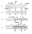
図2および図3は、第1の実施の形態に係る発光装置の製造時における各工程を示す図であり、図4は、製造工程を示すフローチャートである。本実施の形態の発光装置1は、波長変換部2を構成するガラス材21を準備する準備工程(a)、ガラス材21に蛍光体層20a、20bを一体的に設ける波長変換部形成工程(b)、反射部3と基板部4とを所定の精度で位置決めする基板・反射部位置決め工程(c)、反射部3と基板部4との間に隙間が生じないように接合する接合工程(d)、基板部4にLED素子11をLED素子を搭載するLED素子搭載工程(e)、および、波長変換部2と反射部3、基板部4とを一体化する波長変換部一体化工程(f)に基づいて製造される。
2 and 3 are diagrams showing each process in manufacturing the light emitting device according to the first embodiment, and FIG. 4 is a flowchart showing the manufacturing process. In the
(a)準備工程
まず、図2(a)に示すように、シート状ガラス材21を用意し、表面洗浄等の下処理を行う。
(A) Preparatory process First, as shown to Fig.2 (a), the sheet-
(b)波長変換部形成工程
次に、図2(b)に示すように、ガラス材21の表面に増粘材として約1%のニトロセルロースを含むn−酢酸ブチルに蛍光体を溶解した蛍光体溶液を作成し、この溶液をガラス材21の表面にスクリーン印刷して薄膜状に付着させる。次に、蛍光体溶液を印刷されたガラス材21を加熱処理して溶剤分を除去することにより蛍光体層20a、20bを形成する。
(B) Wavelength conversion part formation process Next, as shown in FIG.2 (b), the fluorescence which melt | dissolved the fluorescent substance in the n-butyl acetate which contains about 1% nitrocellulose as a thickener on the surface of the glass material 21 A body solution is prepared, and this solution is screen-printed on the surface of the
(c)基板・反射部位置決め工程
次に、図3(c)に示すように、別工程で反射面30を形成された反射部3と、別工程で配線パターン40を形成された基板部4とを位置決めする。
(C) Substrate / Reflecting Portion Positioning Step Next, as shown in FIG. 3C, the reflecting
(d)接合工程
次に、図3(d)に示すように、反射部3と基板部4とを接着剤等で接合する。このとき、反射部3と基板部4との間に隙間を生じないように行う。
(D) Joining Step Next, as shown in FIG. 3D, the reflecting
(e)LED素子搭載工程
次に、図3(e)に示すように、基板部4の配線パターン40上にLED素子11を金バンプを介しフリップチップ実装する。LED素子11を基板部4に搭載した後、発光部10内にシリコン樹脂を充填してLED素子11を封止する。
(E) LED element mounting process Next, as shown in FIG.3 (e), the
(f)波長変換部一体化工程
次に、図3(f)に示すように、シリコン樹脂による封止をされた発光部10の上面を覆うように波長変換部2を接着剤等で接合する。波長変換部2は、蛍光体層20a、20b、および隙間20cが反射部3との界面に配置されるように接合される。
(F) Wavelength Conversion Unit Integration Step Next, as shown in FIG. 3 (f), the
以下に、発光装置10の動作について説明する。
Below, operation | movement of the light-emitting
基板部4の下面に設けられる図示しない端子部を電源装置に接続して電力を供給すると、発光部10内に設けられたLED素子11が点灯する。LED素子11から放射される光のうち直接透明なシリコン樹脂を透過して蛍光体層20に照射される光は、蛍光体層20を励起する。このことによりLED素子11から放射される光とは異なる波長の励起光が放射される。この励起光と、LED素子11の放射光とが混合されて所定の波長の波長変換光を生じ、このうち上方へ放射された光は、ガラス材21を透過して外部に放射される。また、LED素子11から放射される光のうち蛍光体層20の隙間20cへ放射された光、及び、下方へ放射された光は、幾度か反射した後、蛍光体層20に再度入射するか、あるいは、蛍光体層20の隙間20cから外部放射される。さらに、ガラス材21を透過した光の一部については、ガラスと空気との界面で反射されて蛍光体層20に再度入射する。このことによって蛍光体層20がより効率的に励起される。
When a terminal portion (not shown) provided on the lower surface of the
上記した第1の実施の形態によると、以下の効果が得られる。
(1)波長変換部2と、反射部3と、基板部4とを接着等によって接合して一体化しているので、装置全体を樹脂封止する構成と比べて薄く、かつ、小型化することができる。
(2)蛍光体層20に隙間20cを形成し、蛍光体層20から外部放射されなかった光を外部放射できるようにしたので、外部放射効率を向上することができる。尚、LED素子11から直接隙間20cへ放射される光もガラスと空気の界面で反射されて蛍光体層20に入射するので、外部放射効率を向上することができる。
(3)ガラス材21にスクリーン印刷によって蛍光体を層状に形成するようにしたので、蛍光体層20の厚さにばらつきが生じることがなく、発光装置1の全面にわたって均一で安定した波長変換性が得られる。また、YAG等の高価な蛍光体を使用する場合には、蛍光体を無駄に使用することを防げるので、発光装置1のコストダウンを図れる。
(4)波長変換部2の蛍光体層20を反射部3との界面に配置して封止するようにしたので、装置の厚さを大にすることなく吸湿等による蛍光体の劣化を防ぐことができる。
According to the first embodiment described above, the following effects are obtained.
(1) Since the
(2) Since the
(3) Since the phosphor is formed in layers on the
(4) Since the
なお、第1の実施の形態では、波長変換部2として蛍光体層20とガラス材21とを積層した構成を説明したが、これらは一体的に形成されても良い。例えば、ガラス又は樹脂からなる蛍光体含有材料を薄板状に形成し、反射部3の上面に一体化すると、均一な波長変換性を維持しながら装置全体を更に薄型化することができる。
In the first embodiment, the configuration in which the
また、LED素子11および蛍光体の種類についても、上記した構成以外の種々の組み合わせが可能である、例えば、近紫外光を放射する紫外LED素子とRGB蛍光体との組み合わせに基づく波長変換装置を構成することも可能であり、その他の組み合わせも可能である。また、LED素子の配置数についても所望の数とすることが可能である。
Also, various combinations other than the above-described configuration are possible for the types of
なお、発光装置1の放熱性を高めるものとして、例えば、装置側面に粗面化処理を施して表面積拡大を図ることも可能である。また、銅やアルミニウム等の熱伝導性に優れる金属からなるヒートシンクを設けても良い。
In addition, as a thing which improves the heat dissipation of the light-emitting
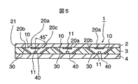
図5は、第1の実施の形態の変形例を示す断面図である。このように発光装置10の反射面30に蛍光体層20bを設けて反射される光を波長変換するようにしても良い。
FIG. 5 is a cross-sectional view showing a modification of the first embodiment. As described above, the
図6は、第2の実施の形態に係る発光装置を示す図であり、(a)は平面図、(b)は(a)のC−C部における断面図である。なお、以下の説明では、第1の実施の形態と共通する部分に共通する引用数字を付して説明している。 6A and 6B are diagrams showing a light-emitting device according to the second embodiment, in which FIG. 6A is a plan view and FIG. 6B is a cross-sectional view taken along a line CC in FIG. In the following description, the same reference numerals as those in the first embodiment are used for description.
第2の実施の形態では、複数の発光部を結合して形成される単一の発光部10に9個のLED素子11をマトリクス状に設けた構成を有し、LED素子11の直上に位置するように正方形状の蛍光体層20を設けている。また、反射面30と基板部4に蛍光体層20を設けてある。なお、図6(a)の構成においては、蛍光体層20は正方形状以外に円形状に形成されても良い。この際、LED素子11に対し、ガラス材21と空気との界面での臨界角以内となる方向には蛍光体層20が設けられていることが望ましい。LED素子11から蛍光体層20へ至らずに外部放射される光がないようにするためである。また、LED素子11の発光波長および蛍光体層20の種類についても、第1の実施の形態で説明したGaN系LED素子と黄色蛍光体との組み合わせに限定されず、用途に応じたものを選択的に用いることができる。
The second embodiment has a configuration in which nine
上記した第2の実施の形態によると、第1の実施の形態の好ましい効果に加えて、発光部10の開口を広く取ることができるので、配線パターン40上へのLED素子11の搭載性が向上する。また、発光部10に対してシリコン樹脂の充填作業を1回行うことによって全てのLED素子11を同時に樹脂封止できるので、生産性に優れるとともに光取り出し性を容易に均一化することができる。
According to the second embodiment described above, in addition to the preferable effects of the first embodiment, the opening of the
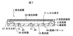
図7は、第3の実施の形態に係る発光装置を示す断面図である。第3の実施の形態の発光装置10は、反射部3の上面を覆う波長変換部2のガラス材21中に薄膜状の蛍光体層20を封入したものである。
FIG. 7 is a cross-sectional view showing a light emitting device according to the third embodiment. In the
波長変換部2は、低融点ガラスからなる第1および第2のガラス材21を用意し、第1および第2のガラス材のいずれか一方に第1の実施の形態で説明した手順で蛍光体層20を形成し、蛍光体層20の形成面を他方のガラスで覆い、これら2つのガラス材を加熱プレスによって熱融着させることにより一体化して形成する。
The
第3の実施の形態によると、薄膜状の蛍光体層20をガラス材21で封止しているので、第1の実施の形態で説明した発光装置1より更なる薄型化を実現することができる。また、蛍光体層20をガラス封止することで蛍光体の吸湿による劣化を防止でき、多湿条件下で使用されるような発光装置であっても長期にわたって安定した波長変換性を付与することが可能となる。なお、ガラス材21の代わりに透明樹脂からなるシート材で蛍光体層20を挟持する構成とすることも可能であるが、樹脂材料については吸湿性を完全に排除することは困難である。
According to the third embodiment, since the thin-
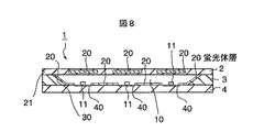
図8は、第4の実施の形態に係る発光装置を示す断面図である。第4の実施の形態の発光装置10は、第3の実施の形態で説明した波長変換部2の蛍光体層20をLED素子11の位置に応じて部分的に配置したものである。
FIG. 8 is a cross-sectional view showing a light emitting device according to the fourth embodiment. In the
第4の実施の形態によると、第3の実施の形態の好ましい効果に加えて蛍光体の使用量を低減できることにより、装置コストを安価にしながら長期にわたって安定した波長変換性を付与することが可能となる。 According to the fourth embodiment, the amount of phosphor used can be reduced in addition to the preferable effects of the third embodiment, so that stable wavelength conversion can be imparted over a long period of time while reducing the apparatus cost. It becomes.
図9は、第5の実施の形態に係る発光装置を示す断面図である。第5の実施の形態の発光装置10は、第4の実施の形態で説明した波長変換部2の光出射面に凹凸を施して光拡散性を付与するようにしたものである。
FIG. 9 is a cross-sectional view showing a light emitting device according to the fifth embodiment. In the
第5の実施の形態によると、第4の実施の形態の好ましい効果に加えて発光装置1から放射される光を広範囲に照射することができ、特に、照明装置等で広範囲に均一な光照射性が要求される用途に好適である。
According to the fifth embodiment, in addition to the preferable effects of the fourth embodiment, it is possible to irradiate light emitted from the
1、発光装置 2、波長変換部 3、反射部 4、基板部 10、発光装置
10、発光部 11、LED素子 20、蛍光体層 21、ガラス材
30、反射面 40、配線パターン 50、発光装置 51、基体
52、反射枠 53、凹部 54、配線 55、LEDチップ
56、波長変換シート 56A、透光性シート基板 56B、波長変換物質層
57、拡散板 58、モールド樹脂
DESCRIPTION OF
Claims (6)
平坦な基体に前記光に基づいて励起される蛍光体を薄膜状に設けた蛍光体層を有する波長変換部を備え、
前記蛍光体層に外部放射のための隙間が形成され、
前記隙間は、前記LED素子に対して前記基体と空気の界面での臨界角以上の領域にのみ形成されることを特徴とする発光装置。 In a light emitting device that arranges a plurality of LED elements in a planar shape and irradiates the light emitted from the LED elements by wavelength conversion,
A phosphor to be excited on the basis of the light on a Tan Taira of substrates provided with a wavelength converter comprising a phosphor layer provided on the thin film,
A gap for external radiation is formed in the phosphor layer ,
The gap is, the light emitting device according to claim Rukoto formed only on the substrate and the critical angle or more areas at the interface of air to the LED element.
Priority Applications (3)
| Application Number | Priority Date | Filing Date | Title |
|---|---|---|---|
| JP2003324570A JP4238681B2 (en) | 2003-09-17 | 2003-09-17 | Light emitting device |
| CNB2004100592617A CN100511732C (en) | 2003-06-18 | 2004-06-15 | Light emitting device |
| US10/869,036 US7498734B2 (en) | 2003-06-18 | 2004-06-17 | Light emitting device with wavelength converted by phosphor |
Applications Claiming Priority (1)
| Application Number | Priority Date | Filing Date | Title |
|---|---|---|---|
| JP2003324570A JP4238681B2 (en) | 2003-09-17 | 2003-09-17 | Light emitting device |
Publications (3)
| Publication Number | Publication Date |
|---|---|
| JP2005093681A JP2005093681A (en) | 2005-04-07 |
| JP2005093681A5 JP2005093681A5 (en) | 2007-08-16 |
| JP4238681B2 true JP4238681B2 (en) | 2009-03-18 |
Family
ID=34455288
Family Applications (1)
| Application Number | Title | Priority Date | Filing Date |
|---|---|---|---|
| JP2003324570A Expired - Fee Related JP4238681B2 (en) | 2003-06-18 | 2003-09-17 | Light emitting device |
Country Status (1)
| Country | Link |
|---|---|
| JP (1) | JP4238681B2 (en) |
Cited By (1)
| Publication number | Priority date | Publication date | Assignee | Title |
|---|---|---|---|---|
| EP4215801A1 (en) * | 2022-01-24 | 2023-07-26 | Analytik Jena US LLC | Light conversion device with high uniformity |
Families Citing this family (28)
| Publication number | Priority date | Publication date | Assignee | Title |
|---|---|---|---|---|
| JP2007003805A (en) * | 2005-06-23 | 2007-01-11 | Hitachi Displays Ltd | Illumination device and display apparatus with same |
| KR100616695B1 (en) * | 2005-10-04 | 2006-08-28 | 삼성전기주식회사 | High power light emitting diode package |
| JP2007123390A (en) * | 2005-10-26 | 2007-05-17 | Kyocera Corp | Light emitting device |
| JP2007123777A (en) | 2005-10-31 | 2007-05-17 | Sharp Corp | Semiconductor light-emitting apparatus |
| KR100618941B1 (en) | 2005-11-08 | 2006-09-01 | 김성규 | Transparent light emitting apparatus and manufacturing method thereof |
| JP5073946B2 (en) * | 2005-12-27 | 2012-11-14 | 新光電気工業株式会社 | Semiconductor device and manufacturing method of semiconductor device |
| JP4752795B2 (en) * | 2007-03-12 | 2011-08-17 | パナソニック株式会社 | Light source device for lighting equipment |
| DE102007046339A1 (en) * | 2007-09-27 | 2009-04-02 | Osram Opto Semiconductors Gmbh | Light source with variable emission characteristics |
| JP5431706B2 (en) * | 2008-10-01 | 2014-03-05 | ミネベア株式会社 | Light emitting device |
| JP5440064B2 (en) * | 2008-10-21 | 2014-03-12 | 東芝ライテック株式会社 | Lighting device |
| JP2011035198A (en) * | 2009-08-03 | 2011-02-17 | Ccs Inc | Method of manufacturing led light-emitting device |
| EP2482351A4 (en) * | 2009-09-25 | 2013-06-05 | Oceans King Lighting Science | Semiconductor light-emitting device and encapsulating method thereof |
| JP5529516B2 (en) * | 2009-12-14 | 2014-06-25 | 株式会社朝日ラバー | LIGHTING DEVICE AND LIGHTING COLOR CHANGE METHOD FOR LIGHTING DEVICE |
| JP5178796B2 (en) * | 2010-09-10 | 2013-04-10 | 三菱電機株式会社 | Light emitting device and lighting device |
| JP2012204349A (en) * | 2011-03-23 | 2012-10-22 | Panasonic Corp | Light-emitting device |
| KR101212654B1 (en) * | 2011-05-20 | 2012-12-14 | (주)라이타이저코리아 | Package for light emitting diode and method for manufacturing thereof |
| JP5724685B2 (en) * | 2011-07-01 | 2015-05-27 | 日本電気硝子株式会社 | Method for manufacturing cell for light emitting device and method for manufacturing light emitting device |
| JP5724684B2 (en) * | 2011-07-01 | 2015-05-27 | 日本電気硝子株式会社 | Cell for light emitting device and light emitting device |
| WO2013061511A1 (en) * | 2011-10-27 | 2013-05-02 | パナソニック株式会社 | Light-emitting device |
| JP2012084924A (en) * | 2012-01-24 | 2012-04-26 | Mitsubishi Electric Corp | Wavelength conversion member |
| JP2013214716A (en) | 2012-03-06 | 2013-10-17 | Nitto Denko Corp | Fluorescent sealing sheet, light emitting diode device, and manufacturing method of light emitting diode device |
| EP2831933B1 (en) * | 2012-03-30 | 2021-05-12 | Lumileds LLC | Optical cavity including a light emitting device and wavelength converting material |
| JP6192897B2 (en) | 2012-04-11 | 2017-09-06 | サターン ライセンシング エルエルシーSaturn Licensing LLC | LIGHT EMITTING DEVICE, DISPLAY DEVICE, AND LIGHTING DEVICE |
| JP2015000036A (en) * | 2013-06-17 | 2015-01-05 | 交和電気産業株式会社 | Illumination device |
| KR101657954B1 (en) | 2014-02-05 | 2016-09-21 | 삼성디스플레이 주식회사 | Backlight assembly and display divece having the same |
| KR20180071027A (en) | 2016-12-19 | 2018-06-27 | 삼성전자주식회사 | Display apparatus |
| US20210397050A1 (en) * | 2018-11-01 | 2021-12-23 | Sharp Kabushiki Kaisha | Backlight device and display device |
| KR102389956B1 (en) * | 2020-02-27 | 2022-04-25 | 주식회사 쉘파스페이스 | Wavelength conversion film and lighting apparatus using the same |
Family Cites Families (6)
| Publication number | Priority date | Publication date | Assignee | Title |
|---|---|---|---|---|
| JP4171107B2 (en) * | 1998-07-09 | 2008-10-22 | スタンレー電気株式会社 | Planar light source |
| JP2002022895A (en) * | 2000-07-04 | 2002-01-23 | Fuji Photo Film Co Ltd | Radiation image conversion panel |
| JP2002299692A (en) * | 2001-03-29 | 2002-10-11 | Mitsubishi Electric Lighting Corp | Reflection type led light source |
| JP2003110146A (en) * | 2001-07-26 | 2003-04-11 | Matsushita Electric Works Ltd | Light-emitting device |
| JP4122738B2 (en) * | 2001-07-26 | 2008-07-23 | 松下電工株式会社 | Method for manufacturing light emitting device |
| JP3707688B2 (en) * | 2002-05-31 | 2005-10-19 | スタンレー電気株式会社 | Light emitting device and manufacturing method thereof |
-
2003
- 2003-09-17 JP JP2003324570A patent/JP4238681B2/en not_active Expired - Fee Related
Cited By (1)
| Publication number | Priority date | Publication date | Assignee | Title |
|---|---|---|---|---|
| EP4215801A1 (en) * | 2022-01-24 | 2023-07-26 | Analytik Jena US LLC | Light conversion device with high uniformity |
Also Published As
| Publication number | Publication date |
|---|---|
| JP2005093681A (en) | 2005-04-07 |
Similar Documents
| Publication | Publication Date | Title |
|---|---|---|
| JP4238681B2 (en) | Light emitting device | |
| JP7125636B2 (en) | light emitting device | |
| TWI758388B (en) | Light emitting device | |
| JP6599295B2 (en) | LIGHT EMITTING ELEMENT HAVING BELT ANGLE REFLECTOR AND MANUFACTURING METHOD | |
| JP5899507B2 (en) | LIGHT EMITTING DEVICE AND LIGHTING DEVICE USING THE SAME | |
| CN100511732C (en) | Light emitting device | |
| KR101209759B1 (en) | Semiconductor light emitting module and method for manufacturing the same | |
| JP5113820B2 (en) | Light emitting device | |
| US8410502B2 (en) | Light-emitting device, planar light source including the light-emitting device, and liquid crystal display device including the planar light source | |
| JP5077130B2 (en) | Lighting device | |
| JP3640153B2 (en) | Illumination light source | |
| JP2007324417A (en) | Semiconductor light-emitting device and manufacturing method therefor | |
| JP6107415B2 (en) | Light emitting device | |
| JP2011114096A (en) | Illumination device | |
| JP2017162942A (en) | Light-emitting device and illuminating device | |
| JP2011096740A (en) | Light-emitting device | |
| JP2019145690A (en) | Light-emitting device and manufacturing method of light-emitting device | |
| JP6079544B2 (en) | Light emitting device and method for manufacturing light emitting device | |
| JP2021106277A (en) | Light-emitting device | |
| US8366307B2 (en) | Semiconductor light emitting device | |
| JP2012009632A (en) | Light-emitting element package and light-emitting element package group with light-emitting element package | |
| JP2010192762A (en) | Semiconductor light emitting device | |
| JP5811770B2 (en) | Light emitting device and manufacturing method thereof | |
| JP5899476B2 (en) | LIGHT EMITTING DEVICE AND LIGHTING DEVICE USING THE SAME | |
| JP2011091126A (en) | Light emitting device (cob module) |
Legal Events
| Date | Code | Title | Description |
|---|---|---|---|
| A621 | Written request for application examination |
Free format text: JAPANESE INTERMEDIATE CODE: A621 Effective date: 20051130 |
|
| A521 | Written amendment |
Free format text: JAPANESE INTERMEDIATE CODE: A523 Effective date: 20070629 |
|
| A977 | Report on retrieval |
Free format text: JAPANESE INTERMEDIATE CODE: A971007 Effective date: 20080730 |
|
| A131 | Notification of reasons for refusal |
Free format text: JAPANESE INTERMEDIATE CODE: A131 Effective date: 20080819 |
|
| RD03 | Notification of appointment of power of attorney |
Free format text: JAPANESE INTERMEDIATE CODE: A7423 Effective date: 20081010 |
|
| A521 | Written amendment |
Free format text: JAPANESE INTERMEDIATE CODE: A523 Effective date: 20081020 |
|
| TRDD | Decision of grant or rejection written | ||
| A01 | Written decision to grant a patent or to grant a registration (utility model) |
Free format text: JAPANESE INTERMEDIATE CODE: A01 Effective date: 20081125 |
|
| A01 | Written decision to grant a patent or to grant a registration (utility model) |
Free format text: JAPANESE INTERMEDIATE CODE: A01 |
|
| A61 | First payment of annual fees (during grant procedure) |
Free format text: JAPANESE INTERMEDIATE CODE: A61 Effective date: 20081208 |
|
| FPAY | Renewal fee payment (event date is renewal date of database) |
Free format text: PAYMENT UNTIL: 20120109 Year of fee payment: 3 |
|
| R150 | Certificate of patent or registration of utility model |
Ref document number: 4238681 Country of ref document: JP Free format text: JAPANESE INTERMEDIATE CODE: R150 Free format text: JAPANESE INTERMEDIATE CODE: R150 |
|
| FPAY | Renewal fee payment (event date is renewal date of database) |
Free format text: PAYMENT UNTIL: 20130109 Year of fee payment: 4 |
|
| FPAY | Renewal fee payment (event date is renewal date of database) |
Free format text: PAYMENT UNTIL: 20140109 Year of fee payment: 5 |
|
| LAPS | Cancellation because of no payment of annual fees |