JP4219084B2 - Preparation method for thin section sample for microscope - Google Patents
Preparation method for thin section sample for microscope Download PDFInfo
- Publication number
- JP4219084B2 JP4219084B2 JP2000345621A JP2000345621A JP4219084B2 JP 4219084 B2 JP4219084 B2 JP 4219084B2 JP 2000345621 A JP2000345621 A JP 2000345621A JP 2000345621 A JP2000345621 A JP 2000345621A JP 4219084 B2 JP4219084 B2 JP 4219084B2
- Authority
- JP
- Japan
- Prior art keywords
- sample
- section
- thin
- ion beam
- focused ion
- Prior art date
- Legal status (The legal status is an assumption and is not a legal conclusion. Google has not performed a legal analysis and makes no representation as to the accuracy of the status listed.)
- Expired - Fee Related
Links
Images

Landscapes
- Analysing Materials By The Use Of Radiation (AREA)
- Sampling And Sample Adjustment (AREA)
Description
【0001】
【発明の属する技術分野】
本発明は、集束イオンビームを用いて電子顕微鏡や原子間力顕微鏡の試料の薄片化加工を行い切り出して試料固定台に確実に固定した顕微鏡用薄片試料作製方法並びにそのようにして作製した顕微鏡用薄片試料に関する。
【0002】
【従来の技術】
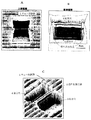
透過型電子顕微鏡の試料は電子の透過像を観察するものであるため、その試料は極めて薄く加工することが求められる。ウェハ等の断面試料を図5に示すような集束イオンビーム装置を用いた薄片化加工によって製作することは周知であって、ウェハ状の試料から機械的に小片を切り出しそれを加工する方法と、ウェハのままエッチング加工して薄片化された試料を取り出す方法とが知られている。前者の加工法は試料とするウェハからまず500μm〜2mm幅、長さ2〜3mm程の小ブロックを切り取り、更に上部を50μm以下に削るという機械加工を要し、この小ブロックの中央加工部分にガス銃14により芳香属ガスやW(CO)6 を吹き付けて保護膜を形成させる。その後集束イオンビーム12を照射して薄片化加工を施し、TEM観察用の断面試料として用いられる。この試料は小ブロックの未加工部分が試料台を兼ねたものとなる。後者の加工法は機械加工をしないで集束イオンビーム装置で直接ウェハから集束イオンビーム加工を実行するものである。この方法は加工部分にまずガス銃14により保護膜DGを形成させて、試料1の面上方から集束イオンビーム12を照射し図4に示すように観察断面の両側をスパッタリング加工により削り取り、観察断面薄片部2の両側に穴3,4を開ける。該穴の大きさは前方穴3が試料台をチルトして観察断面を走査イオン顕微鏡で観察できる程度の大きさに、後方穴4は幅が前方穴3と同じで奥行きは2/3程度に穿設される。図4中Aは加工部分を上部より観察した図であり、Bは走査イオン顕微鏡による断面の観察図そしてCは斜め上方からの顕微鏡観察像である。
【0003】
Bに図示したように試料面をチルトして観察断面として薄片化加工された試料の周辺部に、矢印のように集束イオンビームを走査させて切り込み加工と仕上げ加工を行い、最後にマニピュレータにより操作されるガラスプローブによって該薄片試料切片を保持させ、メッシュ等の試料台上に移動し付着させてTEM観察試料を完成させる。このプロセスを図3に示す。図3のAに示されるようにマニピュレータ(図示されていない)を操作してガラスプローブ7を試料切片21に近づけると該試料切片21は該ガラスプローブ7の先端に静電力によって吸いつけられるように付着し、Bに示すように試料切片21はガラスプローブ7に保持されて薄片化加工部2から切り離される。ガラスプローブ7に保持された試料切片21はCに図示されるようにメッシュ8のような固定台に運ばれて載置される。このメッシュ8等の試料台はコロジオン膜張付きメッシュであったり、マイクログリッドなどの観察や分析などに影響を与えない材質で作られており、試料切片21は膜の粘着力、または静電力によってDに示されるように固定されるものであった。ところが試料台に載置した試料切片21が、保管したり運搬したりウェット処理や試料載置台のハンドリングなどの作業中に試料台から剥がれ遺失してしまうというトラブルがまま生じている。極微小片であるため一旦消失したものは発見は不可能であり、一連の作業が水泡に帰してしまうことになる。
【0004】
【発明が解決しようとする課題】
本発明の課題は、試料台に載置した顕微鏡用の試料切片が、保管したり運搬したり作業中に試料台から剥がれ遺失してしまうことがなく、固定台上に確実に保持される薄片試料を作成する方法と、そのような薄片試料を提供することにある。
【0005】
【課題を解決するための手段】
本発明の薄片試料の固定方法は試料台若しくはメッシュなどの固定台上に載置された薄片試料の所定個所に、ガス銃によってガスを噴射しつつ集束イオンビームを照射するデポジションを施し、これによって、前記固定台に薄片試料を固定するようにした。また、薄片試料は端部において土手状の肉厚部を形成するようにして試料の観察領域が固定作業のデポジションによる再付着を防止するようにした。
【0006】
【発明の実施の形態】
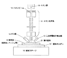
本発明における透過型電子顕微鏡用試料の薄片化加工の方法は図4に示した従来の加工法と同じであり、試料切片21を固定台上に載置するまでのプロセスも図3に示した従来の方法と何ら変りはない。ただ、従来は試料切片21の固定台への固定を図3のDに示したようにメッシュ8の膜の粘着力、または静電力によって行うだけの簡単なものであったが、本発明では試料切片21の所要個所を集束イオンビーム装置を用いたデポジションの手法を応用し、試料切片21を積極的に固定台8に固定してしまおうというものである。本発明に用いる集束イオンビーム装置の概要を図5に示す。これは通常の集束イオンビーム装置であって、イオン源10と、該イオン源10からイオンを引出し集束加速してイオンビーム12を試料面上に偏向走査させるイオン光学系11と、試料を載置し所望角度と位置に駆動制御される試料ステージ15と、試料面にガスを噴射させるガス銃14と、ビーム照射によってよって叩き出された二次荷電粒子を検出する検出器13とから構成される。薄片化加工が施され試料切片21が、マニピュレータ操作されるガラスプローブ7によって表面が不定形の網目状になったマイクログリッドなどの固定台8上に載置されたものを、まず試料ホルダー15’によって集束イオンビーム装置の試料ステージ15上に固定する。固定された固定台8上の試料切片21の所望個所に向けてガス銃14からフェナントレンなどの芳香属ガスやW(CO)6 などのガスを噴射させ、同じ場所に集束イオンビームを照射する。この所望個所は例えば試料切片21のコーナー部分とその周囲の固定台8の領域などである。すると当該領域には保護膜と同様のデポジションが施されることになって、試料切片21を固定台8上に貼付け固定することになる。芳香属ガスを使用したときは炭素のデポジションが、W(CO)6 を用いたときにはタングステンのデポジションが施される。固定に関しては何れを選択してもよいが、ウェット処理など後処理に際し安定性のよいものを選択するとよい。
【0007】
この状態に固定した薄片試料21は、試料台のハンドリング時に固定台8から剥がれ落ちてしまうようなことがないだけでなく、表面の集束イオンビームによるダメージ層の除去を行ったり、表面に選択エッチングを施すなどの該試料を液体中に浸すウェット処理を実施しても試料切片21が固定台8から剥がれてしまうことがない。また、原子間力顕微鏡などのプローブで試料表面を観察したり解析などを行う際に試料切片21が固定台8から落下してしまうこともなく、固定された状態は安定する。
【0008】
この薄片試料は従来、原理上薄い試料を必要とする低加速型電子顕微鏡の試料として使用されてきた。そして、反射型電子顕微鏡の試料は表面からの二次電子を検出するものであるため薄片化は必要ないものと考えられ、半導体を劈開面で割って試料とした劈開試料が使用されていた。しかしインレンズ型電子顕微鏡では試料が厚いと下層部分の情報が混在してしまうため所望個所の情報だけを検出するためには加速電圧を低く押える必要があった。より高分解能像を得ようとする場合、加速度電圧を上げ薄い試料とする要請から従来の薄片試料を使用しようとしても酸を通すなどウェット処理の際に試料が落ちてしまうことが多く適用出来なかった。しかし、本発明によって、薄片試料の固定化が確保できたことを受け薄片化加工をした試料がインレンズ型電子顕微鏡用に適用できるようになった。加速電圧を高くし高感度で解像度のよい顕微鏡観察像が得られるだけでなく、従来の劈開試料と同様にウェット処理などの後処理のノウハウがそのまま使用でき、更に劈開面に限定されない所望個所の断面試料を製作することができるものである。
なお、以上本発明の薄片試料は透過型電子顕微鏡を対象として説明してきたが、本発明による薄片試料の加工法はプローブ顕微鏡(原子間力顕微鏡)用の試料にも適用できることは勿論である。
【0009】
【実施例1】
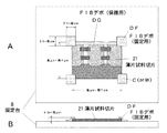
図1に本発明による薄片試料の一実施例を示す。サンプルは透過型電子顕微鏡用の半導体ウェハー(64M DRAMのメモリーセル)断面試料である。加工方法は▲1▼サンプルの所望断面個所を特定してその部分にガスを噴射しつつ集束イオンビームを照射して保護用のデポジションDGを施す。▲2▼断面の前方部分に集束イオンビームを照射しスパッタリングにより前穴を開け、断面を露出させる。▲3▼続いて断面の後方部分に集束イオンビームを照射しスパッタリングにより後穴を開け、断面の薄片化を実行する。▲4▼粗加工によりダメージを受けた断面表面をビーム電流を小さく落したイオンビームにより研磨する。▲5▼試料面をチルトし、穴の底に近い底辺に集束イオンビームにより切り込みを入れる。▲6▼底辺に切り込みを入れる際観察断面にダメージを与えてしまうので、試料面を元に戻して再度研磨する。▲7▼試料の側辺両側に上方からイオンビームを照射して切り込みを入れる。なお、この際のビーム照射は上方から実行するので断面へのダメージは少なく、再研磨の必要はない。▲8▼マニピュレータを操作しながらガラスプローブで切り取られた薄片試料切片21(数μm〜数十μm×数μm〜数十μm)をマイクログリッドの試料台8に載置する。このマイクログリッドは数μmφの不定形の網状体で極めて開口率が高い、透過型電子顕微鏡の試料固定台に最適な構造体である。▲9▼固定台に載置された試料切片の4隅周辺にガス銃でガスを噴射させながら集束イオンビームを照射して図に示すように固定用のデポジションDFを施す。デポジションは図1のAにあるように試料切片の角部分を含む 0.5μm〜数μm四方の領域で、厚みはBに図示されるように0.05μm〜数μmである。この状態で試料切片は固定台に堅固に保持されるので、エッチング用の処理液に浸すウェット処理を施しても固定台から試料切片が剥がれ落ちてしまうようなことはない。
【0010】
【実施例2】
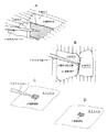
次に示す実施例は、固定用のデポジションを施す際に、試料断面にスパッタ物などが再付着して観察面を汚してしまうことがない工夫を加えた試料加工法で、この方法によって作成された試料を図2に示す。製造過程で先の例と異なるのは▲2▼▲3▼の薄片化加工の部分であり、前穴と後穴を開ける際に試料となる断面部分の厚みを先の例より大きくして残す。そして、試料切片の側辺として切り込みを入れる位置から少し内側にあたる前面部分に土手状の肉厚部分を残して薄片化加工を実行する点が本実施例の特徴であって、仕上がった薄片試料の断面として示される図2のBに土手状の肉厚部22として示される形態である。薄片化加工の過程でこの様に細工しておくことで、後の▲9▼試料切片を固定台に固定するデポジション工程の時、集束イオンビームの照射によってスパッタリングされた試料片が試料中央の観察部分に飛んできて再付着することを効果的に防止することができるのである。すなわち、この土手状の肉厚部22が試料中央方向へのスパッタリングによる飛散を遮蔽する機能を果たす。
なお、図2のAには試料台として採用したマイクログリッド8のスポンジ形態を部分的に示した。マイクログリッドはこのように不定形の網状体で極めて開口率が高いので、透過型電子顕微鏡の試料台として好適な素材といえる。
【0011】
【発明の効果】
以上説明したように、本発明の薄片試料の固定方法は試料台若しくはメッシュなどの固定台上に載置された薄片試料の所定個所に、ガス銃によってガスを噴射しつつ集束イオンビームを照射するデポジションを施し、これによって、前記固定台に薄片試料を固定するようにしたので、試料を保管したり運搬中やウェット処理や試料載置台のハンドリングなどの作業中に試料台から剥がれ遺失してしまうというような事故は回避できる。また、原子間力顕微鏡のプローブを用いた解析作業を行っても作業中に試料切片が剥がれ落ちてしまうようなこともなく、安定した試験検査が実行できる。
また、薄片試料は端部において土手状の肉厚部を形成するようにすると、その土手状の肉厚部が試料切片を固定台に固定するデポジション工程の時、集束イオンビームの照射によってスパッタリングされた試料片が試料中央の観察部分に飛んできて再付着することを効果的に防止することができるのである。
【0012】
本発明を顕微鏡の試料作製に適用した場合には、従来インレンズタイプの走査型電子顕微鏡の加速電圧を低く押えなければならなかった問題を解決し、加速電圧を高くし高感度で解像度のよい顕微鏡観察像が得られるだけでなく、従来の劈開試料と同様にウェット処理などの後処理のノウハウがそのまま使用でき、更に劈開面に限定されない所望個所の断面試料を製作することができるものである。
【図面の簡単な説明】
【図1】本発明によって作成した透過型電子顕微鏡用試料の一実施例を示す図で、Aはその平面図、Bはその正面図である。
【図2】本発明によって作成した透過型電子顕微鏡用試料の他の実施例を示す図で、Aはその平面図、Bはその正面図である。
【図3】薄片化加工した試料を固定台上に載置する工程を示す図である。
【図4】試料(ウェハー)を薄片化加工した状態を示す図である。
【図5】本発明に使用される集束イオンビーム装置概略構成図である。
【符号の説明】
1 試料 10 イオン源
2 薄片化加工部 11 イオン光学系
21 試料切片 12 イオンビーム
22 土手状厚肉部 13 二次荷電粒子検出器
3 前方穴 14 ガス銃
4 後方穴 15 試料ステージ
7 ガラスプローブ 15’試料ホルダー
8 固定台 DF 固定用デポジション
(メッシュ、マイクログリッド) DG 保護用デポジション[0001]
BACKGROUND OF THE INVENTION
The present invention was created manufactured in the securely fixed as thin sample preparation method as well as for microscope cut performed sliced processed sample fixing base samples electron microscope or atomic force microscope using a focused ion beam microscope The present invention relates to a thin film sample.
[0002]
[Prior art]
Since the sample of the transmission electron microscope is for observing an electron transmission image, it is required to process the sample extremely thinly. It is well known that a cross-sectional sample such as a wafer is manufactured by thinning using a focused ion beam apparatus as shown in FIG. 5, and a method of mechanically cutting a small piece from a wafer-like sample and processing it, There is known a method of taking out a thinned sample by etching with a wafer. The former processing method requires a machining process in which a small block having a width of 500 μm to 2 mm and a length of 2 to 3 mm is first cut from a sample wafer, and the upper part is further cut to 50 μm or less. A protective film is formed by spraying aromatic gas or W (CO) 6 with a gas gun 14. After that, the focused ion beam 12 is irradiated to make a thin piece and used as a cross-sectional sample for TEM observation. In this sample, the unprocessed portion of the small block also serves as the sample stage. In the latter processing method, focused ion beam processing is executed directly from a wafer by a focused ion beam apparatus without machining. In this method, a protective film DG is first formed on a processed portion by a gas gun 14, irradiated with a focused ion beam 12 from above the surface of the sample 1, and both sides of the observation cross section are scraped off by sputtering as shown in FIG. Holes 3 and 4 are made on both sides of the thin piece 2. The size of the hole is such that the front hole 3 tilts the sample stage and the observation cross section can be observed with a scanning ion microscope. The rear hole 4 has the same width as the front hole 3 and the depth is about 2/3. Drilled. In FIG. 4, A is a view of the processed portion observed from above, B is an observation view of a cross section by a scanning ion microscope, and C is a microscope observation image from obliquely above.
[0003]
As shown in Fig. B, the sample surface is tilted and sliced as an observation cross section, and the focused ion beam is scanned as shown by the arrow on the periphery of the sample to perform cutting and finishing, and finally the manipulator is used for operation. The sliced sample section is held by the glass probe to be moved and moved onto a sample table such as a mesh to complete the TEM observation sample. This process is illustrated in FIG. As shown in FIG. 3A, when the manipulator (not shown) is operated to bring the glass probe 7 close to the
[0004]
[Problems to be solved by the invention]
The problem of the present invention is that the sample section for the microscope placed on the sample stage does not peel off from the sample stage during storage or transportation or work, and is thinly held on the fixed stage. It is to provide a method of making a sample and such a flake sample.
[0005]
[Means for Solving the Problems]
In the thin sample fixing method of the present invention, deposition is performed by irradiating a focused ion beam while injecting a gas with a gas gun at a predetermined position of a thin sample placed on a fixed table such as a sample table or a mesh. Thus, the thin sample was fixed to the fixing table. Further, the thin sample was formed with a bank-like thick portion at the end so that the observation area of the sample was prevented from being reattached due to the deposition of the fixing work.
[0006]
DETAILED DESCRIPTION OF THE INVENTION
The method of thinning the transmission electron microscope sample in the present invention is the same as the conventional processing method shown in FIG. 4, and the process until the
[0007]
The
[0008]
Conventionally, this thin sample has been used as a sample for a low-acceleration electron microscope that requires a thin sample in principle. Since the sample of the reflection electron microscope detects secondary electrons from the surface, it is considered that thinning is not necessary, and a cleaved sample obtained by dividing a semiconductor by a cleavage plane has been used. However, in the in-lens electron microscope, if the sample is thick, information on the lower layer is mixed, so that it is necessary to keep the acceleration voltage low in order to detect only information at a desired location. When trying to obtain a higher resolution image, it is not possible to apply a thin sample due to the demand for a thin sample by increasing the acceleration voltage, and the sample often drops during wet processing, such as passing acid, even if trying to use a thin sample. It was. However, in accordance with the present invention, since the fixation of the thin sample can be ensured, the thinned sample can be applied to the in-lens electron microscope. Not only can the acceleration voltage be increased to obtain a high-sensitivity, high-resolution image of the microscope, but also the know-how of post-processing such as wet processing can be used as in the case of conventional cleaved samples. A cross-sectional sample can be manufactured.
Although the thin sample of the present invention has been described for the transmission electron microscope, the processing method of the thin sample according to the present invention can of course be applied to a sample for a probe microscope (atomic force microscope).
[0009]
[Example 1]
FIG. 1 shows an embodiment of a flake sample according to the present invention. The sample is a cross-sectional sample of a semiconductor wafer (64M DRAM memory cell) for a transmission electron microscope. The processing method is as follows: (1) A desired cross-sectional portion of a sample is specified, and a focused ion beam is irradiated while gas is sprayed on the portion, and a protective deposition DG is applied. (2) A focused ion beam is irradiated to the front part of the cross section, a front hole is formed by sputtering, and the cross section is exposed. ▲ 3 ▼ subsequently opened rear hole by sputtering by irradiating a focused ion beam to the rear portion of the cross section, executes a thinning of the cross section. (4) The surface of the cross section damaged by the roughing process is polished by an ion beam with a reduced beam current. (5) Tilt the sample surface and make a cut with a focused ion beam at the bottom near the bottom of the hole. {Circle around (6)} Since the observation cross section is damaged when the cut is made in the bottom side, the sample surface is returned to the original and polished again. (7) Irradiate the ion beam from above on both sides of the sample to make a cut. In addition, since the beam irradiation at this time is performed from above, there is little damage to the cross section, and re-polishing is not necessary. (8) A thin sample section 21 (several μm to several tens of μm × several μm to several tens of μm) cut with a glass probe while operating the manipulator is placed on a sample table 8 of a microgrid. This microgrid is an irregular structure of several μmφ and an extremely high aperture ratio, and is an optimum structure for a sample fixing base of a transmission electron microscope. {Circle around (9)} A fixed deposition DF is applied as shown in the figure by irradiating a focused ion beam while injecting gas with a gas gun around the four corners of the sample section placed on the fixing table. As shown in FIG. 1A, the deposition is a 0.5 μm to several μm square region including the corner of the sample section, and the thickness is 0.05 μm to several μm as shown in B. In this state, since the sample section is firmly held on the fixing base, the sample section is not peeled off from the fixing base even if wet processing is performed soaking in the etching processing solution.
[0010]
[Example 2]
The following example is a sample processing method with a device that prevents spatters from adhering to the sample cross-section and soiling the observation surface when performing deposition for fixation. The obtained sample is shown in FIG. The difference from the previous example in the manufacturing process is the thinning part of (2) (3), and when the front hole and the rear hole are made, the thickness of the cross-sectional part that becomes a sample is left larger than the previous example. . And the point of executing the thinning process leaving a bank-like thick part on the front part which is slightly inward from the position where the cut is made as the side of the sample section is a feature of this example, and the finished thin piece sample It is a form shown as bank-like
2A partially shows a sponge form of the
[0011]
【The invention's effect】
As described above, the thin sample specimen fixing method of the present invention irradiates a focused ion beam while injecting a gas with a gas gun to a predetermined portion of a thin specimen sample placed on a sample base or a fixed base such as a mesh. Since the thin sample was fixed to the fixed table by this, the sample was stored and transported, and it was peeled off from the sample table during work such as wet processing and sample mounting table. Accidents such as Further, even if an analysis operation using an atomic force microscope probe is performed, the sample section is not peeled off during the operation, and a stable test inspection can be performed.
In addition, if the thin sample is formed with a bank-like thick part at the end, the bank-like thick part is sputtered by irradiation with a focused ion beam during the deposition process in which the sample section is fixed to a fixed base. Thus, it is possible to effectively prevent the formed sample piece from flying and reattaching to the observation portion in the center of the sample.
[0012]
When the present invention is applied to the preparation of a microscope sample, the problem that the acceleration voltage of the conventional in-lens scanning electron microscope had to be kept low was solved, the acceleration voltage was increased, the sensitivity was high, and the resolution was good. Not only can a microscope observation image be obtained, but also post-processing know-how such as wet processing can be used as it is with a conventional cleaved sample, and a cross-sectional sample at a desired location that is not limited to a cleaved surface can be produced. .
[Brief description of the drawings]
FIG. 1 is a view showing an example of a transmission electron microscope sample prepared according to the present invention, in which A is a plan view and B is a front view thereof.
FIGS. 2A and 2B are diagrams showing another embodiment of a transmission electron microscope sample prepared according to the present invention, in which A is a plan view and B is a front view thereof.
FIG. 3 is a diagram illustrating a process of placing a thinned sample on a fixed base.
FIG. 4 is a view showing a state in which a sample (wafer) is processed into a thin piece.
FIG. 5 is a schematic configuration diagram of a focused ion beam apparatus used in the present invention.
[Explanation of symbols]
1 Sample 10 Ion source 2 Thinning section 11 Ion optical system
21 Sample section 12 Ion beam
22 Bank-like thick part 13 Secondary charged particle detector 3 Front hole 14 Gas gun 4 Back hole 15 Sample stage 7 Glass probe 15 '
Claims (2)
Priority Applications (1)
| Application Number | Priority Date | Filing Date | Title |
|---|---|---|---|
| JP2000345621A JP4219084B2 (en) | 2000-11-13 | 2000-11-13 | Preparation method for thin section sample for microscope |
Applications Claiming Priority (1)
| Application Number | Priority Date | Filing Date | Title |
|---|---|---|---|
| JP2000345621A JP4219084B2 (en) | 2000-11-13 | 2000-11-13 | Preparation method for thin section sample for microscope |
Publications (2)
| Publication Number | Publication Date |
|---|---|
| JP2002148162A JP2002148162A (en) | 2002-05-22 |
| JP4219084B2 true JP4219084B2 (en) | 2009-02-04 |
Family
ID=18819623
Family Applications (1)
| Application Number | Title | Priority Date | Filing Date |
|---|---|---|---|
| JP2000345621A Expired - Fee Related JP4219084B2 (en) | 2000-11-13 | 2000-11-13 | Preparation method for thin section sample for microscope |
Country Status (1)
| Country | Link |
|---|---|
| JP (1) | JP4219084B2 (en) |
Families Citing this family (4)
| Publication number | Priority date | Publication date | Assignee | Title |
|---|---|---|---|---|
| JP2010141221A (en) * | 2008-12-15 | 2010-06-24 | Shin-Etsu Chemical Co Ltd | Method of manufacturing silicon substrate with oxide film |
| JP5492115B2 (en) * | 2011-02-10 | 2014-05-14 | 日本電子株式会社 | Preparation method of needle-like sample for electron microscope |
| JP2012168027A (en) * | 2011-02-15 | 2012-09-06 | Sumitomo Metal Mining Co Ltd | Method of preparing sample for electron microscope |
| CN107817147B (en) * | 2017-11-07 | 2024-05-10 | 中国地质大学(武汉) | Similar material preparation facilities of simulation ground body joint face |
-
2000
- 2000-11-13 JP JP2000345621A patent/JP4219084B2/en not_active Expired - Fee Related
Also Published As
| Publication number | Publication date |
|---|---|
| JP2002148162A (en) | 2002-05-22 |
Similar Documents
| Publication | Publication Date | Title |
|---|---|---|
| JP2774884B2 (en) | Method for separating sample and method for analyzing separated sample obtained by this separation method | |
| US10283317B2 (en) | High throughput TEM preparation processes and hardware for backside thinning of cross-sectional view lamella | |
| JP3957750B2 (en) | Ion beam preparation device for electron microscopy | |
| US8723144B2 (en) | Apparatus for sample formation and microanalysis in a vacuum chamber | |
| KR102221931B1 (en) | Method of Performing Electron Diffraction Pattern Analysis Upon a Sample | |
| US6395347B1 (en) | Micromachining method for workpiece observation | |
| US7276691B2 (en) | Ion beam device and ion beam processing method | |
| US6300631B1 (en) | Method of thinning an electron transparent thin film membrane on a TEM grid using a focused ion beam | |
| US20090053395A1 (en) | Method and System for Imaging a Cross Section of a Specimen | |
| EP1804273B1 (en) | Method for specimen preparation | |
| JP3711018B2 (en) | TEM sample thinning method | |
| CN104737266B (en) | Charged particle beam device and sample preparation method | |
| JP4219084B2 (en) | Preparation method for thin section sample for microscope | |
| JP2007108105A (en) | Method for preparing sample for electron microscope, converged ion beam device and a sample support stand | |
| JP3132938B2 (en) | Charged beam device for cross-section processing observation and processing method | |
| JP2004095339A (en) | Ion beam device and ion beam processing method | |
| US6362475B1 (en) | Scanning electron microscope/energy dispersive spectroscopy sample preparation method and sample produced thereby | |
| JP2000230891A (en) | Method for preparing sample for transmission electron microscope | |
| JP3106846U (en) | Sample holder for charged particle beam equipment | |
| JPH11160210A (en) | Observation sample for transmission electron microscope and its preparation | |
| JPH08313415A (en) | Transmission electron microscope sample preparation method and focused ion beam processing apparatus | |
| EP1612836A2 (en) | Method for the removal of a microscopic sample from a substrate | |
| JPH10227728A (en) | Surface analysis sample and manufacture thereof | |
| Teshima | Combining FIB and automated microcleaving provides fast, accurate cross sections | |
| KR20050041312A (en) | Method for fabricating a sample of semiconductor |
Legal Events
| Date | Code | Title | Description |
|---|---|---|---|
| RD01 | Notification of change of attorney |
Free format text: JAPANESE INTERMEDIATE CODE: A7421 Effective date: 20040303 |
|
| A711 | Notification of change in applicant |
Free format text: JAPANESE INTERMEDIATE CODE: A712 Effective date: 20040526 |
|
| A621 | Written request for application examination |
Free format text: JAPANESE INTERMEDIATE CODE: A621 Effective date: 20060105 |
|
| A977 | Report on retrieval |
Free format text: JAPANESE INTERMEDIATE CODE: A971007 Effective date: 20071214 |
|
| A131 | Notification of reasons for refusal |
Free format text: JAPANESE INTERMEDIATE CODE: A131 Effective date: 20071218 |
|
| A521 | Written amendment |
Free format text: JAPANESE INTERMEDIATE CODE: A523 Effective date: 20080215 |
|
| A131 | Notification of reasons for refusal |
Free format text: JAPANESE INTERMEDIATE CODE: A131 Effective date: 20080325 |
|
| A521 | Written amendment |
Free format text: JAPANESE INTERMEDIATE CODE: A523 Effective date: 20080523 |
|
| A131 | Notification of reasons for refusal |
Free format text: JAPANESE INTERMEDIATE CODE: A131 Effective date: 20080826 |
|
| A521 | Written amendment |
Free format text: JAPANESE INTERMEDIATE CODE: A523 Effective date: 20080929 |
|
| TRDD | Decision of grant or rejection written | ||
| A01 | Written decision to grant a patent or to grant a registration (utility model) |
Free format text: JAPANESE INTERMEDIATE CODE: A01 Effective date: 20081104 |
|
| A01 | Written decision to grant a patent or to grant a registration (utility model) |
Free format text: JAPANESE INTERMEDIATE CODE: A01 |
|
| A61 | First payment of annual fees (during grant procedure) |
Free format text: JAPANESE INTERMEDIATE CODE: A61 Effective date: 20081111 |
|
| FPAY | Renewal fee payment (event date is renewal date of database) |
Free format text: PAYMENT UNTIL: 20111121 Year of fee payment: 3 |
|
| R150 | Certificate of patent or registration of utility model |
Free format text: JAPANESE INTERMEDIATE CODE: R150 Ref document number: 4219084 Country of ref document: JP Free format text: JAPANESE INTERMEDIATE CODE: R150 |
|
| RD01 | Notification of change of attorney |
Free format text: JAPANESE INTERMEDIATE CODE: A7421 Effective date: 20091108 |
|
| FPAY | Renewal fee payment (event date is renewal date of database) |
Free format text: PAYMENT UNTIL: 20111121 Year of fee payment: 3 |
|
| RD03 | Notification of appointment of power of attorney |
Free format text: JAPANESE INTERMEDIATE CODE: R3D03 |
|
| FPAY | Renewal fee payment (event date is renewal date of database) |
Free format text: PAYMENT UNTIL: 20111121 Year of fee payment: 3 |
|
| FPAY | Renewal fee payment (event date is renewal date of database) |
Free format text: PAYMENT UNTIL: 20121121 Year of fee payment: 4 |
|
| FPAY | Renewal fee payment (event date is renewal date of database) |
Free format text: PAYMENT UNTIL: 20121121 Year of fee payment: 4 |
|
| FPAY | Renewal fee payment (event date is renewal date of database) |
Free format text: PAYMENT UNTIL: 20131121 Year of fee payment: 5 |
|
| FPAY | Renewal fee payment (event date is renewal date of database) |
Free format text: PAYMENT UNTIL: 20131121 Year of fee payment: 5 |
|
| S531 | Written request for registration of change of domicile |
Free format text: JAPANESE INTERMEDIATE CODE: R313531 |
|
| S533 | Written request for registration of change of name |
Free format text: JAPANESE INTERMEDIATE CODE: R313533 |
|
| FPAY | Renewal fee payment (event date is renewal date of database) |
Free format text: PAYMENT UNTIL: 20131121 Year of fee payment: 5 |
|
| R350 | Written notification of registration of transfer |
Free format text: JAPANESE INTERMEDIATE CODE: R350 |
|
| FPAY | Renewal fee payment (event date is renewal date of database) |
Free format text: PAYMENT UNTIL: 20131121 Year of fee payment: 5 |
|
| FPAY | Renewal fee payment (event date is renewal date of database) |
Free format text: PAYMENT UNTIL: 20131121 Year of fee payment: 5 |
|
| R250 | Receipt of annual fees |
Free format text: JAPANESE INTERMEDIATE CODE: R250 |
|
| R250 | Receipt of annual fees |
Free format text: JAPANESE INTERMEDIATE CODE: R250 |
|
| R250 | Receipt of annual fees |
Free format text: JAPANESE INTERMEDIATE CODE: R250 |
|
| R250 | Receipt of annual fees |
Free format text: JAPANESE INTERMEDIATE CODE: R250 |
|
| R250 | Receipt of annual fees |
Free format text: JAPANESE INTERMEDIATE CODE: R250 |
|
| R250 | Receipt of annual fees |
Free format text: JAPANESE INTERMEDIATE CODE: R250 |
|
| LAPS | Cancellation because of no payment of annual fees |