JP2010141221A - Method of manufacturing silicon substrate with oxide film - Google Patents
Method of manufacturing silicon substrate with oxide film Download PDFInfo
- Publication number
- JP2010141221A JP2010141221A JP2008317847A JP2008317847A JP2010141221A JP 2010141221 A JP2010141221 A JP 2010141221A JP 2008317847 A JP2008317847 A JP 2008317847A JP 2008317847 A JP2008317847 A JP 2008317847A JP 2010141221 A JP2010141221 A JP 2010141221A
- Authority
- JP
- Japan
- Prior art keywords
- silicon substrate
- oxide film
- holder
- groove
- manufacturing
- Prior art date
- Legal status (The legal status is an assumption and is not a legal conclusion. Google has not performed a legal analysis and makes no representation as to the accuracy of the status listed.)
- Pending
Links
Images
Abstract
Description
本発明は、膜厚が5μm以上のシリコン酸化膜を有し、鏡面加工面に実質的に凸部がない酸化膜付きシリコン基板の製造方法に関する。 The present invention relates to a method for manufacturing a silicon substrate with an oxide film having a silicon oxide film having a thickness of 5 μm or more and having substantially no convex portion on a mirror-finished surface.
酸化シリコンからなる酸化膜がついたシリコン基板は、熱酸化法やCVD法で製造され、半導体分野で広く使用されている。半導体分野では、この酸化膜は絶縁膜としての機能を利用するため、酸化膜厚は比較的薄く、数百オングストローム程度のものが使われている。 A silicon substrate having an oxide film made of silicon oxide is manufactured by a thermal oxidation method or a CVD method and widely used in the semiconductor field. In the semiconductor field, since this oxide film uses the function as an insulating film, the oxide film thickness is comparatively thin, and several hundred angstroms are used.
一方、光通信用の光導波路型デバイスやMEMS(Micro Electro Mechanical System)でも酸化膜付きシリコン基板が用いられているが、半導体分野と比較して格段に厚い酸化膜が望まれており、しばしばその膜厚は5μm以上、時には20μm程度の厚さの酸化膜が必要とされている。 On the other hand, silicon substrates with oxide films are also used in optical waveguide devices for optical communication and MEMS (Micro Electro Mechanical System). An oxide film having a thickness of 5 μm or more and sometimes about 20 μm is required.
半導体分野で広く使われている熱酸化法では、単純な作業で緻密且つ高品質な酸化膜がシリコン基板の表裏両面に形成できる。この方法では、酸化の進行は酸素原子の拡散則に従い、酸化膜厚の2乗と酸化時間が比例する関係を持つことが知られている。つまり、酸化膜厚が厚くなればなるほど、酸化に必要な時間は大きく増大することになる。 In the thermal oxidation method widely used in the semiconductor field, a dense and high-quality oxide film can be formed on both the front and back surfaces of a silicon substrate by a simple operation. In this method, it is known that the progress of oxidation follows the diffusion rule of oxygen atoms and has a relationship in which the square of the oxide film thickness is proportional to the oxidation time. That is, the thicker the oxide film thickness, the greater the time required for oxidation.
高速酸化法として、ポリシリコンを熱酸化する方法(例えば特許文献1及び2参照)が報告されている。その製造方法は、「ポリシリコンを基板上に堆積し、その基板を酸化熱処理してポリシリコン層を酸化する」、という工程を所望する酸化膜厚に達するまで繰り返す方法である。このため工程が煩雑になり、実質的な製造効率は改善され難い。また、酸化膜表面の荒れや、シリコン基板の片面のみに厚い酸化膜が形成されるため、後工程において熱応力分布の不均一さによって基板に反りが生じやすいという品質的な問題もある。
As a fast oxidation method, a method of thermally oxidizing polysilicon (see, for example,
上記とは異なる高速酸化法として、加圧容器内で、酸化性雰囲気として水蒸気を含む雰囲気とする方法があり、酸化温度1000℃で厚さ15μmの酸化膜を製造する時間は150時間程度と製造効率という点では優れている。 As a high-speed oxidation method different from the above, there is a method in which an atmosphere containing water vapor is used as an oxidizing atmosphere in a pressurized container, and the time for producing an oxide film having a thickness of 15 μm at an oxidation temperature of 1000 ° C. is about 150 hours. It is excellent in terms of efficiency.
熱酸化法、ポリシリコンを加熱する方法および水蒸気による熱酸化法で酸化膜が例えば2μm程度の比較的薄い酸化膜を形成するときは、酸化時間が短いために、シリコン基板とそれを保持するジグの接触面に生じる凸部の高さは高々0.05μm程度であり、この高さならばデバイスを作成する回路形成上問題が生じないとされる。 When a relatively thin oxide film having a thickness of, for example, about 2 μm is formed by a thermal oxidation method, a method of heating polysilicon, or a thermal oxidation method using water vapor, since the oxidation time is short, the silicon substrate and the jig for holding it The height of the convex portion generated on the contact surface is about 0.05 μm at most, and if this height is reached, there is no problem in forming a circuit for producing a device.
しかし、酸化膜厚が5μm以上と厚い酸化膜付きシリコン基板では、酸化時間は、熱酸化法の場合、膜厚の2乗に比例して長時間化するため、シリコン基板とジグとの接触時間が長くなり、例えば5μmの酸化膜を形成した場合、ジグ周辺部分の鏡面加工面に約0.4μm程度の凸部が生じ、この結果、光導波路デバイスの特性がこの部分で劣化するという不具合が生じる。 However, in the case of a silicon substrate with a thick oxide film having an oxide film thickness of 5 μm or more, in the case of the thermal oxidation method, the oxidation time becomes longer in proportion to the square of the film thickness, so the contact time between the silicon substrate and the jig For example, when an oxide film of 5 μm is formed, a convex portion of about 0.4 μm is formed on the mirror-finished surface around the jig, and as a result, there is a problem that the characteristics of the optical waveguide device deteriorate at this portion. Arise.
本発明は上記問題点に鑑みてなされたものであって、パターン形成面となるシリコン基板の鏡面加工面上にジグ跡のない高品質の酸化膜を有する酸化膜付きシリコン基板の製造方法を提供することを目的とする。 The present invention has been made in view of the above problems, and provides a method of manufacturing a silicon substrate with an oxide film having a high-quality oxide film having no jig trace on the mirror-finished surface of the silicon substrate that is to be a pattern forming surface. The purpose is to do.
上記課題を解決するため、本発明は、エッジ面取り加工が施されたシリコン基板を、少なくとも対向する側板と、該側板間に連結される溝を有する複数の支持棒とを具備するホルダに保持して、酸化性雰囲気下で熱処理することで表面に酸化膜を形成する酸化膜付きシリコン基板の製造方法において、前記シリコン基板の保持は、前記ホルダに具備された前記支持棒の溝と、前記シリコン基板の最外周端部及び面取り加工部の少なくとも一方とを接触させることのみで為すことを特徴とする酸化膜付きシリコン基板の製造方法を提供する(請求項1)。 In order to solve the above-mentioned problems, the present invention holds a silicon substrate subjected to edge chamfering processing in a holder including at least opposing side plates and a plurality of support bars having grooves connected between the side plates. In the method of manufacturing a silicon substrate with an oxide film, in which an oxide film is formed on the surface by heat treatment in an oxidizing atmosphere, the silicon substrate is held by the groove of the support rod provided in the holder, and the silicon Provided is a method of manufacturing a silicon substrate with an oxide film, which is performed only by bringing at least one of the outermost peripheral end portion and the chamfered portion of the substrate into contact with each other.
このように、シリコン基板の保持は、シリコン基板を保持するホルダに具備された支持棒の溝と、シリコン基板の最外周端部から面取り加工部のみとを接触させることで行う。そして、その保持されたシリコン基板を熱処理してシリコン基板の表面に酸化膜を形成することで、シリコン基板の鏡面加工面上に、シリコン基板を保持するホルダによるジグ跡のない酸化膜を形成することができる。そのため、シリコン基板の鏡面加工面上に高品質の酸化膜を有する酸化膜付きシリコン基板を得ることができ、その酸化膜付きシリコン基板を光導波路デバイスに用いる場合に特性の劣化を生じないパターン形成面を持つ酸化膜付きシリコン基板を製造することができる。 As described above, the silicon substrate is held by bringing the groove of the support rod provided in the holder holding the silicon substrate into contact with only the chamfered portion from the outermost peripheral end of the silicon substrate. Then, the held silicon substrate is heat-treated to form an oxide film on the surface of the silicon substrate, thereby forming an oxide film free from jig marks by the holder that holds the silicon substrate on the mirror-finished surface of the silicon substrate. be able to. Therefore, a silicon substrate with an oxide film having a high-quality oxide film on the mirror-finished surface of the silicon substrate can be obtained, and pattern formation that does not cause deterioration of characteristics when the silicon substrate with an oxide film is used in an optical waveguide device A silicon substrate with an oxide film having a surface can be manufactured.
この場合、シリコン基板を保持するホルダに具備された支持棒の溝の深さhが、シリコン基板の面取り加工部の長さWより小さいようにすることができる(請求項2)。
このように、本発明では、支持棒の溝の深さhをシリコン基板の面取り加工部の長さWより小さくすることで、シリコン基板の最外周端部から面取り加工部のみがホルダに具備された支持棒の溝と接触し、鏡面加工部(シリコン基板の主面)はホルダと接触しない状態でシリコン基板を保持できる。そのため、シリコン基板の鏡面加工面上に、シリコン基板を保持するホルダによるジグ跡のない酸化膜を形成することができる。
In this case, the depth h of the groove of the support rod provided in the holder for holding the silicon substrate can be made smaller than the length W of the chamfered portion of the silicon substrate.
Thus, in the present invention, the holder is provided with only the chamfered portion from the outermost peripheral end portion of the silicon substrate by making the depth h of the groove of the support rod smaller than the length W of the chamfered portion of the silicon substrate. The mirror processing part (the main surface of the silicon substrate) is in contact with the groove of the support rod, and can hold the silicon substrate without contacting the holder. Therefore, it is possible to form an oxide film free from jig marks by the holder that holds the silicon substrate on the mirror-finished surface of the silicon substrate.
また、この場合、シリコン基板を保持するホルダに具備された支持棒の溝の深さhが、シリコン基板の面取り加工部の長さWより大きく、且つ前記溝の開角αを面取り加工部の成す角より大きいようにすることができる(請求項3)。
このように、本発明では、支持棒の溝の深さhをシリコン基板の面取り加工部の長さWより大きくし、且つ溝の開角αを面取り面の成す角より大きくすることで、シリコン基板の最外周端部から面取り加工部のみがホルダに具備された支持棒の溝と接触し、鏡面加工部はホルダと接触しない状態でシリコン基板を保持できる。そのため、シリコン基板の鏡面加工面上に、シリコン基板を保持するホルダによるジグ跡のない酸化膜を形成することができる。
Further, in this case, the depth h of the groove of the support rod provided in the holder for holding the silicon substrate is larger than the length W of the chamfered portion of the silicon substrate, and the opening angle α of the groove is the chamfered portion of the chamfered portion. It can be made larger than the formed angle (Claim 3).
Thus, in the present invention, the depth h of the groove of the support rod is made larger than the length W of the chamfered portion of the silicon substrate, and the opening angle α of the groove is made larger than the angle formed by the chamfered surface. Only the chamfered portion is in contact with the groove of the support rod provided in the holder from the outermost peripheral end portion of the substrate, and the mirror-finished portion can hold the silicon substrate without being in contact with the holder. Therefore, it is possible to form an oxide film free from jig marks by the holder that holds the silicon substrate on the mirror-finished surface of the silicon substrate.
さらに、この場合、形成する酸化膜の厚さを5μm以上とすることができる(請求項4)。
このように、本発明ではシリコン基板に形成する酸化膜の厚さが5μm以上と厚い場合であっても、シリコン基板の鏡面加工面上に、シリコン基板を保持するホルダによるジグ跡のない酸化膜を形成することができる。そのため、従来の方法では、光導波路デバイスを作成する際に発生していた回路形成上の問題を解消した酸化膜付きシリコン基板を製造することができる。
Furthermore, in this case, the thickness of the oxide film to be formed can be 5 μm or more.
As described above, in the present invention, even when the thickness of the oxide film formed on the silicon substrate is as thick as 5 μm or more, the oxide film is free from jig marks by the holder that holds the silicon substrate on the mirror-finished surface of the silicon substrate. Can be formed. Therefore, according to the conventional method, it is possible to manufacture a silicon substrate with an oxide film that solves the problem of circuit formation that has occurred when producing an optical waveguide device.
また、本発明の製造方法は、前記酸化性雰囲気が水蒸気を含むことができる(請求項5)。
このように、酸化性雰囲気が水蒸気を含むことで、例えば、酸化温度1000℃で厚さ15μmの酸化膜を製造する時間は150時間程度であり、効率良く酸化膜付きシリコン基板を製造することができる。そのため、従来の方法では光導波路デバイスを作成する際に発生していた回路形成上の問題を解消した酸化膜付きシリコン基板を製造することができる。
In the production method of the present invention, the oxidizing atmosphere may contain water vapor (Claim 5).
Thus, when the oxidizing atmosphere contains water vapor, for example, the time for producing an oxide film having a thickness of 15 μm at an oxidation temperature of 1000 ° C. is about 150 hours, and thus a silicon substrate with an oxide film can be produced efficiently. it can. Therefore, it is possible to manufacture a silicon substrate with an oxide film that solves the problem of circuit formation that has occurred when an optical waveguide device is produced by the conventional method.
以上説明したように、本発明の酸化膜付きシリコン基板の製造方法は、シリコン基板の保持は、シリコン基板を保持するホルダに具備された支持棒の溝と、シリコン基板の最外周端部から面取り加工部のみとを接触させることで行う。そして、その保持されたシリコン基板を熱処理してシリコン基板の表面に酸化膜を形成することで、シリコン基板の鏡面加工面上に、シリコン基板を保持するホルダのジグ跡のない酸化膜を形成することができる。そのため、光導波路デバイスに用いる場合、パターン形成面となるシリコン基板の鏡面加工面上に、高品質の酸化膜を有する酸化膜付きシリコン基板を製造することができる。 As described above, in the method for manufacturing a silicon substrate with an oxide film according to the present invention, the silicon substrate is held by chamfering from the groove of the support rod provided in the holder for holding the silicon substrate and the outermost peripheral edge of the silicon substrate. This is done by contacting only the processed part. Then, the held silicon substrate is heat-treated to form an oxide film on the surface of the silicon substrate, thereby forming an oxide film without a jig trace of the holder that holds the silicon substrate on the mirror-finished surface of the silicon substrate. be able to. Therefore, when used for an optical waveguide device, a silicon substrate with an oxide film having a high-quality oxide film can be manufactured on the mirror-finished surface of the silicon substrate that serves as a pattern formation surface.
以下、本発明についてより具体的に説明する。
前述したように、この厚い酸化膜を製造するときの問題点としては、酸化膜表面の品質があり、光導波路デバイスに用いると特性が劣化するという不具合が生じていた。
Hereinafter, the present invention will be described more specifically.
As described above, as a problem when manufacturing this thick oxide film, there is a quality of the oxide film surface, and there is a problem that the characteristics deteriorate when used in an optical waveguide device.
この酸化膜表面の品質の問題とは、例えば、膜厚が5μmの酸化膜を形成した場合、シリコン基板の鏡面加工面に高さ約0.4μm程度の凸部が生じることであり、この凸部が光導波路デバイスの機能部となるコア層に伝播し、コア層の形状を崩すために光導波路デバイスの特性が劣化したものと考えられる。
また、この凸部は、酸化膜が2μm程度の比較的薄い酸化膜を形成したときは、高さは0.05μm程度であり、この高さであればデバイスを作製する回路形成上問題が生じないことがわかった。
The problem of the quality of the oxide film surface is that, for example, when an oxide film having a film thickness of 5 μm is formed, a convex portion having a height of about 0.4 μm is formed on the mirror-finished surface of the silicon substrate. It is considered that the characteristics of the optical waveguide device are deteriorated because the portion propagates to the core layer serving as the functional portion of the optical waveguide device and the shape of the core layer is destroyed.
In addition, when a relatively thin oxide film with an oxide film of about 2 μm is formed, the height of this convex part is about 0.05 μm, and this height causes a problem in circuit formation for manufacturing a device. I knew it was n’t there.
そこで、本発明者等は、酸化膜表面の品質の劣化の原因となる凸部を形成することなく、シリコン基板に厚い酸化膜を形成することに想到し、シリコン基板の保持は、シリコン基板を保持するホルダに具備された支持棒の溝と、シリコン基板の最外周端部から面取り加工部のみとを接触させることで行い、その保持されたシリコン基板を熱処理してシリコン基板の表面に酸化膜を形成することで、シリコン基板の鏡面加工面上に、シリコン基板を保持するホルダによるジグ跡のない厚い酸化膜を形成することを試みた。 Accordingly, the present inventors have conceived that a thick oxide film is formed on a silicon substrate without forming convex portions that cause deterioration of the quality of the oxide film surface. The support rod groove provided in the holder to be held is brought into contact with only the chamfered portion from the outermost peripheral end of the silicon substrate, and the held silicon substrate is heat-treated to form an oxide film on the surface of the silicon substrate. In this way, an attempt was made to form a thick oxide film free from jig marks by a holder for holding the silicon substrate on the mirror-finished surface of the silicon substrate.
その結果、シリコン基板の鏡面加工面上に、シリコン基板を保持するホルダによるジグ跡のない厚い酸化膜を形成することができ、光導波路デバイスに用いる場合、パターン形成面となるシリコン基板の鏡面加工面上に、高品質の酸化膜を有する酸化膜付きシリコン基板を得ることができた。 As a result, it is possible to form a thick oxide film without a jig trace by a holder that holds the silicon substrate on the mirror-finished surface of the silicon substrate, and when used for an optical waveguide device, the mirror-finishing of the silicon substrate that becomes the pattern formation surface A silicon substrate with an oxide film having a high quality oxide film on the surface could be obtained.
本発明は、上記の発見に基づいて完成されたものであり、以下、本発明について図面を参照しながらさらに詳細に説明するが、本発明はこれらに限定されるものではない。
ここで、図1は本発明の熱処理装置の構成例を模式的に示す図である。
The present invention has been completed based on the above findings, and the present invention will be described in more detail below with reference to the drawings. However, the present invention is not limited to these.
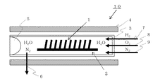
Here, FIG. 1 is a diagram schematically showing a configuration example of the heat treatment apparatus of the present invention.
この熱処理装置10は、シリコン基板1を加熱するための円筒状カンタルヒータ4と、ヒータ4の内側に同軸に配設された石英製炉心管3を備えている。ヒータ4は3等分に分割され、炉心管3内を±1℃以内に均熱化できる。炉心管3の尾部には、ノズル7〜9が挿入され、それぞれのノズル7〜9からは、水素、酸素、キャリヤガスとして窒素が供給される。また、炉心管3のノズル7〜9と反対側の下部には、排気管6が設けられていて、炉心管3は炭化珪素製のキャップ5で閉じることができる。
The
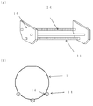
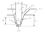
さらに、シリコン基板1を保持するための、図2(a)のような対向する側板16と該側板間に連結される溝14を有する複数の支持棒11とを具備した石英製ホルダ2が炉心管3内に配設され、このホルダ2によって、シリコン基板1が等間隔に保持される。ここで、図2(b)は本発明の熱処理装置においてホルダに具備された支持棒により保持されたシリコン基板を示す要部断面図であり、図3と図5は本発明の熱処理装置において溝深さが異なるホルダに保持されたシリコン基板を模式的に示す図である。また、このときの本発明の熱処理装置におけるホルダに具備された支持棒の溝の形状を図4と図6に示す。
Further, a
図2のように、ホルダ2に具備された複数の支持棒11によりシリコン基板1を保持することで、シリコン基板1とホルダ2との接触箇所が少ない状態でシリコン基板1が保持される。この場合、支持棒11の数は3本ではなく、2本あるいは4本以上有していてもよい。
As shown in FIG. 2, the
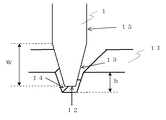
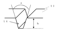
図3のように、ホルダ2に具備された支持棒11の溝14の深さhを、面取り加工部13の長さWよりも小さくすることで、シリコン基板1の最外周端部12から面取り加工部13のみがホルダ2に具備された支持棒11の溝14と接触し、鏡面加工面15はホルダ2と接触しない状態でシリコン基板1が保持される。このホルダ2に具備された支持棒11の溝14の形状は、シリコン基板1の最外周端部12から面取り加工部13のみがホルダ2に具備された支持棒11の溝14と接触するものであれば限定されず、図4あるいは図6に示すような形状であってもよい。
As shown in FIG. 3, the depth h of the
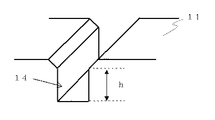
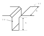
また、図5のように、ホルダ2に具備された支持棒11の溝14の深さhを、面取り加工部13の長さWよりも大きくし、且つホルダ2に具備された支持棒11の溝14の開角αが基板面取り部の面取り面の成す角βより大きくすることで、シリコン基板1の最外周端部12から面取り加工部13のみが、ホルダ2に具備された支持棒11の溝14と接触し、鏡面加工面15はホルダ2と接触しない状態でシリコン基板1が保持される。
なお、基板の支持点は下側からの支持が1または2箇所、横側からは2箇所の支持、合計3から4箇所の支持が望ましい。
Further, as shown in FIG. 5, the depth h of the
In addition, as for the support point of a board | substrate, the support from a lower side is 1 or 2 places, the support from 2 places from a horizontal side, and a total of 3 to 4 places support is desirable.
図3または図5のように、シリコン基板を保持して、熱処理することで、シリコン基板の鏡面加工面15上に、シリコン基板を保持するホルダによるジグ跡のない酸化膜を形成することができる熱処理装置とすることができる。そのため、光導波路デバイスに用いる場合、パターン形成面となるシリコン基板の鏡面加工面上に、高品質の酸化膜を有する酸化膜付きシリコン基板を得ることができ、光導波路デバイスにおける特性の劣化を生じない酸化膜を形成することができる熱処理装置とすることができる。
As shown in FIG. 3 or FIG. 5, an oxide film without a jig mark by the holder that holds the silicon substrate can be formed on the mirror-finished
次に、本発明の酸化膜付きシリコン基板の製造方法の一例を図面を参照しながらさらに詳細に説明するが、本発明はこれらに限定されるわけではない。 Next, although an example of the manufacturing method of the silicon substrate with an oxide film of this invention is demonstrated in detail, referring drawings, this invention is not necessarily limited to these.
まず最初に、図4または図6に示すようなホルダ2に具備された支持棒11の溝14に、エッジ面取り加工が施されたシリコン基板1をセットする。そして、図1に示すような熱処理装置の炉心管3内に、シリコン基板1を保持したホルダ2を挿入して、キャップ5で炉心管3を閉じる。
First, the
次に、ノズル7から水素、ノズル8から酸素、ノズル9からキャリアガスの窒素をそれぞれ供給し、熱反応させることにより、炉心管3内で水蒸気を生成して水蒸気を含む雰囲気を作る。また、ヒータ4により、炉心管3内を熱処理温度±1℃以内に均熱化し、シリコン基板1を加熱して、シリコン基板1の表面に所望膜厚の酸化膜を形成する。なお、酸化膜の形成法としては、熱酸化法であれば良く、常圧酸化または加圧酸化は使用する装置や形成する酸化膜厚の都合等で選択することができる。
Next, hydrogen is supplied from the nozzle 7, oxygen is supplied from the nozzle 8, and nitrogen as a carrier gas is supplied from the nozzle 9 to cause a thermal reaction, thereby generating water vapor in the
このように、本発明の酸化膜付きシリコン基板の製造方法は、図3または図5のように、ホルダ2に具備された支持棒11の溝14とシリコン基板1の最外周端部12から面取り加工部13のみとを接触させることでシリコン基板1を保持し、その保持されたシリコン基板1を水蒸気を含む雰囲気下において熱処理することでシリコン基板1の表面に酸化膜を形成する。これにより、シリコン基板の鏡面加工面上に、シリコン基板を保持するホルダによるジグ跡のない酸化膜を形成することができる。そのため、シリコン基板の鏡面加工面上に高品質の酸化膜を有する酸化膜付きシリコン基板を得ることができ、その酸化膜付きシリコン基板を光導波路デバイスに用いる場合に特性の劣化を生じないパターン形成面を持つ酸化膜付きシリコン基板を製造することができる。
As described above, the method of manufacturing the silicon substrate with an oxide film according to the present invention is chamfered from the
また、本発明の酸化膜付きシリコン基板の製造方法では、形成する酸化膜の厚さを5μm以上とすることができる。
本発明では、シリコン基板に形成する酸化膜の厚さが5μm以上と厚い場合であっても、シリコン基板の鏡面加工面上に、シリコン基板を保持するホルダによるジグ跡のない酸化膜を形成することができる。そのため、従来の方法では、光導波路デバイスを作成する際、酸化膜表面にジグ跡として生じる凸部が影響し、発生していたパターン形成面における回路形成上の問題を解消することができる酸化膜付きシリコン基板を製造することができる。
Moreover, in the manufacturing method of the silicon substrate with an oxide film of this invention, the thickness of the oxide film to form can be 5 micrometers or more.
In the present invention, even if the thickness of the oxide film formed on the silicon substrate is as thick as 5 μm or more, an oxide film without a jig trace by the holder that holds the silicon substrate is formed on the mirror-finished surface of the silicon substrate. be able to. Therefore, in the conventional method, when producing an optical waveguide device, the convex portion generated as a jig trace affects the surface of the oxide film, and the oxide film that can solve the problem of circuit formation on the pattern forming surface that has occurred An attached silicon substrate can be manufactured.
次に本発明の実施例、比較例を示して本発明をより具体的に説明するが、本発明はこれらに限定されるものではない。
(実施例1)
直径100mmのシリコン基板上に所定膜厚として10μmの酸化膜を形成した。このとき、シリコン基板の熱処理には、図1に示すような熱処理装置を用いた。この熱処理装置を用いた酸化膜の形成手順は、以下のとおりである。
Next, the present invention will be described more specifically with reference to Examples and Comparative Examples of the present invention, but the present invention is not limited to these.
Example 1
An oxide film having a thickness of 10 μm was formed on a silicon substrate having a diameter of 100 mm. At this time, a heat treatment apparatus as shown in FIG. 1 was used for heat treatment of the silicon substrate. The procedure for forming an oxide film using this heat treatment apparatus is as follows.
まず、図1のような直径400mm、長さ2500mmの円筒状カンタルヒータ4の中に、これと同軸に直径350mm、長さ2000mmの石英製炉心管3をセットする。ヒータ4で炉心管3内を1000℃±1℃以内に均熱化する。炉心管3の尾部に3本の直径10mm、長さ200mmのノズル7〜9を挿入し、それぞれのノズルから水素3.6L/min、酸素2.0L/min、キャリヤガスとして窒素25L/minをそれぞれ供給する。そして、熱反応させることにより、炉心管3内で水蒸気を生成して水蒸気を含む雰囲気を作り出す。シリコン基板1を石英製のホルダ2に具備された支持棒11の溝14に等間隔にセットして炉心管3に挿入し、炭化珪素製のキャップ5で閉じ、酸化条件を設定して熱処理を行い、シリコン基板1の表面に酸化膜を形成する。
First, a
このとき、シリコン基板1を保持するホルダ2に具備された支持棒11は、図6のような形状の溝を有しており、その溝の深さhは2.0mm、上部の幅が2.0mmで、溝の角度αを30度に加工したものを用いた。また、使用したシリコン基板の直径は200mm、厚さは725μmで、エッジ面取り加工の角度は25度、面取り加工部の長さWは0.6mmであった。このシリコン基板を図6のような形状の溝を有する支持棒を具備したホルダによって、最外周部から面取り加工部のみを接触させて保持した。酸化条件としては、高圧酸化条件として、ヒータ設定温度1000℃、炉心管内圧力5気圧で、70時間の酸化を行った。
At this time, the support rod 11 provided in the
その結果、平均膜厚が10.7μmの酸化膜を育成し、かつ、鏡面加工面上の酸化膜にジグ跡がない酸化膜付きシリコン基板50枚を得ることができた。また、シリコン基板の外周面を観察した結果、ホルダに具備された支持棒の溝と接触したシリコン基板の面取り加工部にジグ跡として白濁領域が観察されたが、鏡面加工面上には外観上の異常はなく、ジグ跡は認められなかった。 As a result, an oxide film having an average film thickness of 10.7 μm was grown, and 50 oxide-coated silicon substrates having no jig trace on the mirror-finished surface could be obtained. In addition, as a result of observing the outer peripheral surface of the silicon substrate, a cloudy region was observed as a jig trace in the chamfered portion of the silicon substrate in contact with the groove of the support rod provided in the holder. There was no abnormality and no jig trace was observed.
(実施例2)
実施例1と同様の手順で、図1に示すような熱処理装置を用いてシリコン基板を熱処理し、酸化膜を形成した。
このとき、シリコン基板1を保持するホルダ2に具備された支持棒11は、図4のような形状の溝を有しており、その溝の幅が1.0mmで、深さhを0.5mmに加工したものを用いた。また、使用したシリコン基板の直径は200mm、厚さは725μmで、エッジ面取り加工部の長さWは0.6mmであった。このシリコン基板を図4のような形状の溝を有する支持棒を具備したホルダによって、最外周部から面取り加工部のみを接触させて保持した。また、酸化条件は、実施例1と同様に高圧酸化条件として、ヒータ設定温度1000℃、炉心管内圧力5気圧で、70時間の酸化を行った。
(Example 2)
In the same procedure as in Example 1, the silicon substrate was heat-treated using a heat treatment apparatus as shown in FIG. 1 to form an oxide film.
At this time, the support rod 11 provided in the
その結果、平均膜厚が10.5μmの酸化膜を育成し、かつ、鏡面加工面上の酸化膜にジグ跡がない酸化膜付きシリコン基板50枚を得ることができた。また、シリコン基板の外周面を観察した結果、ホルダに具備された支持棒の溝と接触したシリコン基板の面取り加工部にジグ跡として白濁領域が観察されたが、鏡面加工面上には外観上の異常はなく、ジグ跡は認められなかった。 As a result, an oxide film having an average film thickness of 10.5 μm was grown, and 50 oxide-coated silicon substrates having no jig traces on the mirror-finished surface could be obtained. In addition, as a result of observing the outer peripheral surface of the silicon substrate, a cloudy region was observed as a jig trace in the chamfered portion of the silicon substrate in contact with the groove of the support rod provided in the holder. There was no abnormality and no jig trace was observed.
(比較例)
実施例1と同様の手順で、従来の熱処理装置を用いてシリコン基板を熱処理し、酸化膜を形成した。
このとき、シリコン基板1を保持するホルダ2に具備された支持棒11は、図7のような形状の溝を有しており、その溝の幅が1.0mmで、深さhを2.0mmに加工したものを用いた。また、使用したシリコン基板の直径は200mm、厚さは725μmで、エッジ面取り加工部の長さWは0.6mmであった。このシリコン基板を図7のような形状の溝を有する支持棒を具備したホルダによって、最外周部から面取り加工部だけでなく、鏡面加工面も接触させて保持した。また、酸化条件は、実施例1と同様に高圧酸化条件として、ヒータ設定温度1000℃、炉心管内圧力5気圧で、70時間の酸化を行った。
尚、比較例のホルダに具備された支持棒の溝の深さは、実施例のものより深いため、ホルダの厚さAは実施例より薄くされる。
(Comparative example)
In the same procedure as in Example 1, the silicon substrate was heat treated using a conventional heat treatment apparatus to form an oxide film.
At this time, the support rod 11 provided in the
In addition, since the depth of the groove | channel of the support bar with which the holder of the comparative example was equipped is deeper than the thing of an Example, the thickness A of a holder is made thinner than an Example.
その結果、平均膜厚が10.6μmの酸化膜を育成したシリコン基板を50枚得ることができた。しかし、シリコン基板を取り出した後にシリコン基板の外周付近を観察した結果、50枚のシリコン基板のうち、37枚の鏡面加工面上の酸化膜に約2mm2程度の大きさの白濁領域が観察された。この領域をHRP(KLA Tencor社製)で高さを測定した結果、その高さは2.8μmであった。また、SEM−EDXで元素分析を行った結果、シリコンと酸素元素が観察された。このことにより、シリコン基板とホルダに具備された支持棒の溝との接触面付近で優先的にシリコン酸化膜が形成され、これが凸部となっていることがわかった。 As a result, 50 silicon substrates on which an oxide film having an average film thickness of 10.6 μm was grown could be obtained. However, as a result of observing the vicinity of the outer periphery of the silicon substrate after the silicon substrate was taken out, a cloudiness region having a size of about 2 mm 2 was observed on the oxide film on 37 mirror-finished surfaces of the 50 silicon substrates. It was. As a result of measuring the height of this region with HRP (manufactured by KLA Tencor), the height was 2.8 μm. In addition, as a result of elemental analysis by SEM-EDX, silicon and oxygen elements were observed. Thus, it was found that the silicon oxide film was formed preferentially in the vicinity of the contact surface between the silicon substrate and the groove of the support rod provided in the holder, and this was a convex portion.
以上のことから、実施例1及び実施例2は、シリコン基板の鏡面加工面上に、シリコン基板を保持するホルダによるジグ跡のない酸化膜を形成することができたが、比較例は、シリコン基板の鏡面加工面上に、凸部が生じてしまい、高品質の酸化膜を得ることはできなかった。 From the above, Example 1 and Example 2 were able to form an oxide film without a jig trace by a holder that holds the silicon substrate on the mirror-finished surface of the silicon substrate. Convex portions were formed on the mirror-finished surface of the substrate, and a high-quality oxide film could not be obtained.
このように、本発明の酸化膜付きシリコン基板の製造方法によれば、シリコン基板の鏡面加工面上に、シリコン基板を保持するホルダによるジグ跡のない酸化膜を形成することができる。そのため、シリコン基板の鏡面加工面上に高品質の酸化膜を有する酸化膜付きシリコン基板を得ることができ、その酸化膜付きシリコン基板を光導波路デバイスに用いる場合に特性の劣化を生じないパターン形成面を持つ酸化膜付きシリコン基板を製造することができる。 Thus, according to the manufacturing method of the silicon substrate with an oxide film of the present invention, an oxide film without a jig trace by the holder holding the silicon substrate can be formed on the mirror-finished surface of the silicon substrate. Therefore, a silicon substrate with an oxide film having a high-quality oxide film on the mirror-finished surface of the silicon substrate can be obtained, and pattern formation that does not cause deterioration of characteristics when the silicon substrate with an oxide film is used in an optical waveguide device A silicon substrate with an oxide film having a surface can be manufactured.
また、本発明の熱処理装置は、シリコン基板の鏡面加工面上に、シリコン基板を保持するホルダによるジグ跡のない酸化膜を形成することができ、光導波路デバイスに用いる場合、パターン形成面となるシリコン基板の鏡面加工面上に、高品質の酸化膜を形成することができる。よって、光導波路デバイスにおける回路形成上の問題を生じない酸化膜を形成することができる熱処理装置とすることができる。 Further, the heat treatment apparatus of the present invention can form an oxide film without a jig trace by a holder for holding a silicon substrate on the mirror-finished surface of the silicon substrate, and when used for an optical waveguide device, it becomes a pattern formation surface. A high-quality oxide film can be formed on the mirror-finished surface of the silicon substrate. Therefore, a heat treatment apparatus capable of forming an oxide film that does not cause a problem in circuit formation in the optical waveguide device can be obtained.
尚、本発明は、上記実施形態に限定されるものではない。上記実施形態は、例示であり、本発明の特許請求の範囲に記載された技術的思想と実質的に同一な構成を有し、同様な作用効果を奏するものは、いかなるものであっても本発明の技術的範囲に包含される。 The present invention is not limited to the above embodiment. The above-described embodiment is an exemplification, and the present invention has substantially the same configuration as the technical idea described in the claims of the present invention, and any device that exhibits the same function and effect is the present invention. It is included in the technical scope of the invention.
1…シリコン基板、 2…ホルダ、 3…炉心管、 4…ヒータ、 5…キャップ、 6…排気管、 7…ノズル、 8…ノズル、 9…ノズル、 10…熱処理装置、 11…支持棒、 12…最外周端部、 13…面取り加工部、 14…溝、 15…鏡面加工面、 16…側板。
DESCRIPTION OF
Claims (5)
Priority Applications (1)
| Application Number | Priority Date | Filing Date | Title |
|---|---|---|---|
| JP2008317847A JP2010141221A (en) | 2008-12-15 | 2008-12-15 | Method of manufacturing silicon substrate with oxide film |
Applications Claiming Priority (1)
| Application Number | Priority Date | Filing Date | Title |
|---|---|---|---|
| JP2008317847A JP2010141221A (en) | 2008-12-15 | 2008-12-15 | Method of manufacturing silicon substrate with oxide film |
Publications (1)
| Publication Number | Publication Date |
|---|---|
| JP2010141221A true JP2010141221A (en) | 2010-06-24 |
Family
ID=42351075
Family Applications (1)
| Application Number | Title | Priority Date | Filing Date |
|---|---|---|---|
| JP2008317847A Pending JP2010141221A (en) | 2008-12-15 | 2008-12-15 | Method of manufacturing silicon substrate with oxide film |
Country Status (1)
| Country | Link |
|---|---|
| JP (1) | JP2010141221A (en) |
Cited By (1)
| Publication number | Priority date | Publication date | Assignee | Title |
|---|---|---|---|---|
| JP2014118631A (en) * | 2012-12-19 | 2014-06-30 | Kaneka Corp | Substrate holder and method of manufacturing solar cell substrate |
Citations (8)
| Publication number | Priority date | Publication date | Assignee | Title |
|---|---|---|---|---|
| JPS62134233U (en) * | 1986-02-18 | 1987-08-24 | ||
| JPS6430825U (en) * | 1987-08-19 | 1989-02-27 | ||
| JPH01308043A (en) * | 1988-06-06 | 1989-12-12 | Mitsubishi Electric Corp | Boat replacing device for semiconductor wafer |
| JPH0233428U (en) * | 1988-08-26 | 1990-03-02 | ||
| JPH09139389A (en) * | 1995-11-13 | 1997-05-27 | F T L:Kk | Jig for manufacturing semiconductor device and manufacture of semiconductor device |
| JP2002148162A (en) * | 2000-11-13 | 2002-05-22 | Seiko Instruments Inc | Slice sample fixing method and sample using it |
| JP2003192328A (en) * | 2001-12-06 | 2003-07-09 | Kst World Co Ltd | Method for generating silicon dioxide film |
| JP2003309076A (en) * | 2002-04-15 | 2003-10-31 | Shin Etsu Handotai Co Ltd | Port for heat treating semiconductor wafer and its manufacturing method |
-
2008
- 2008-12-15 JP JP2008317847A patent/JP2010141221A/en active Pending
Patent Citations (8)
| Publication number | Priority date | Publication date | Assignee | Title |
|---|---|---|---|---|
| JPS62134233U (en) * | 1986-02-18 | 1987-08-24 | ||
| JPS6430825U (en) * | 1987-08-19 | 1989-02-27 | ||
| JPH01308043A (en) * | 1988-06-06 | 1989-12-12 | Mitsubishi Electric Corp | Boat replacing device for semiconductor wafer |
| JPH0233428U (en) * | 1988-08-26 | 1990-03-02 | ||
| JPH09139389A (en) * | 1995-11-13 | 1997-05-27 | F T L:Kk | Jig for manufacturing semiconductor device and manufacture of semiconductor device |
| JP2002148162A (en) * | 2000-11-13 | 2002-05-22 | Seiko Instruments Inc | Slice sample fixing method and sample using it |
| JP2003192328A (en) * | 2001-12-06 | 2003-07-09 | Kst World Co Ltd | Method for generating silicon dioxide film |
| JP2003309076A (en) * | 2002-04-15 | 2003-10-31 | Shin Etsu Handotai Co Ltd | Port for heat treating semiconductor wafer and its manufacturing method |
Cited By (1)
| Publication number | Priority date | Publication date | Assignee | Title |
|---|---|---|---|---|
| JP2014118631A (en) * | 2012-12-19 | 2014-06-30 | Kaneka Corp | Substrate holder and method of manufacturing solar cell substrate |
Similar Documents
| Publication | Publication Date | Title |
|---|---|---|
| TWI707971B (en) | Combined anneal and selective deposition process | |
| JP3761546B2 (en) | Method for manufacturing SiC single crystal substrate | |
| TW201738971A (en) | Combined anneal and selective deposition systems | |
| JP5015419B2 (en) | Surface treatment method of metal carbide substrate used in semiconductor manufacturing process, and metal carbide substrate | |
| JP2019026500A (en) | METHOD FOR MANUFACTURING SINGLE CRYSTAL SiC, METHOD FOR MANUFACTURING SiC INGOT, METHOD FOR MANUFACTURING SiC WAFER, AND SINGLE CRYSTAL SiC | |
| JP2008222509A (en) | METHOD FOR PRODUCING SINGLE CRYSTAL SUBSTRATE WITH SiC EPITAXIAL FILM | |
| JP2010141221A (en) | Method of manufacturing silicon substrate with oxide film | |
| JP2009064955A (en) | Manufacturing method for silicon carbide semiconductor device | |
| JP5352156B2 (en) | Heat treatment equipment | |
| WO2003048041A1 (en) | Method for creating silicon dioxide film | |
| CN108447772A (en) | A kind of manufacturing method of COOLMOS silicon epitaxial wafers | |
| JP6399171B2 (en) | Silicon member and method for manufacturing silicon member | |
| JP6141130B2 (en) | Method for manufacturing silicon carbide semiconductor device | |
| JP6894606B2 (en) | Method for producing graphene and graphene film produced by it | |
| JP5087375B2 (en) | Method for manufacturing silicon carbide semiconductor device | |
| JP4603865B2 (en) | Manufacturing method of silicon substrate with oxide film and silicon substrate with oxide film | |
| KR102105367B1 (en) | Heat treatment method | |
| US9679799B2 (en) | Process for fabricating a semiconductor-on-insulator substrate | |
| JP2014528895A (en) | Method for forming a graphene layer on a substrate surface including a silicon layer | |
| JP2016016998A (en) | Method for producing carbon film | |
| JP2010087019A (en) | Method for manufacturing semiconductor device, thermal oxidizing processing method, and thermal oxidizing processing apparatus | |
| US20020118942A1 (en) | Method for producing an optical waveguide substrate and an optical waveguide substrate | |
| JP2006216566A (en) | Heater supporting device, semiconductor manufacturing device, and manufacturing method of semiconductor device | |
| JP2017088452A (en) | Method for producing carbon nanostructure, and carbon nanostructure production device | |
| JPH06163439A (en) | Semiconductor diffusion oven boat and manufacture thereof |
Legal Events
| Date | Code | Title | Description |
|---|---|---|---|
| A621 | Written request for application examination |
Free format text: JAPANESE INTERMEDIATE CODE: A621 Effective date: 20101026 |
|
| A977 | Report on retrieval |
Free format text: JAPANESE INTERMEDIATE CODE: A971007 Effective date: 20110909 |
|
| A131 | Notification of reasons for refusal |
Free format text: JAPANESE INTERMEDIATE CODE: A131 Effective date: 20110920 |
|
| A521 | Written amendment |
Free format text: JAPANESE INTERMEDIATE CODE: A523 Effective date: 20111111 |
|
| A02 | Decision of refusal |
Free format text: JAPANESE INTERMEDIATE CODE: A02 Effective date: 20120328 |