JP4199397B2 - Semiconductor device mounting structure - Google Patents
Semiconductor device mounting structure Download PDFInfo
- Publication number
- JP4199397B2 JP4199397B2 JP35941299A JP35941299A JP4199397B2 JP 4199397 B2 JP4199397 B2 JP 4199397B2 JP 35941299 A JP35941299 A JP 35941299A JP 35941299 A JP35941299 A JP 35941299A JP 4199397 B2 JP4199397 B2 JP 4199397B2
- Authority
- JP
- Japan
- Prior art keywords
- plating layer
- zinc
- circuit wiring
- semiconductor element
- copper
- Prior art date
- Legal status (The legal status is an assumption and is not a legal conclusion. Google has not performed a legal analysis and makes no representation as to the accuracy of the status listed.)
- Expired - Fee Related
Links
Images

Classifications
-
- H—ELECTRICITY
- H10—SEMICONDUCTOR DEVICES; ELECTRIC SOLID-STATE DEVICES NOT OTHERWISE PROVIDED FOR
- H10W—GENERIC PACKAGES, INTERCONNECTIONS, CONNECTORS OR OTHER CONSTRUCTIONAL DETAILS OF DEVICES COVERED BY CLASS H10
- H10W90/00—Package configurations
- H10W90/701—Package configurations characterised by the relative positions of pads or connectors relative to package parts
- H10W90/721—Package configurations characterised by the relative positions of pads or connectors relative to package parts of bump connectors
- H10W90/724—Package configurations characterised by the relative positions of pads or connectors relative to package parts of bump connectors between a chip and a stacked insulating package substrate, interposer or RDL
Landscapes
- Chemically Coating (AREA)
- Wire Bonding (AREA)
Description
【0001】
【発明の属する技術分野】
本発明は、各種電子デバイスに使用される半導体素子の実装構造体に関するものである。
【0002】
【従来の技術】
従来より、半導体素子の実装方法としてフェースダウンボンディングが知られている。
【0003】
このフェースダウンボンディングに使用される半導体素子の下面には、高密度にパターン形成された電子回路以外に複数個の端子が設けられており、これら複数個の端子を絶縁基板上面の対応する回路配線に半田接合させることにより半導体素子が絶縁基板上に実装される。
【0004】
尚、前記回路配線の形成には、加工の容易性等からアルミニウムが一般的に使用されており、この場合、半田接合される回路配線の上面には半田濡れ性の向上のために、ニッケルめっき層及び金めっき層が順次、被着されていた。
【0005】
【発明が解決しようとする課題】
ところで、この従来の実装構造体においては、アルミニウムから成る回路配線上にニッケルめっき層を析出させる際の触媒として、通常、パラジウムが使用されている。
【0006】
しかしながら、パラジウムを触媒として使用した場合、パラジウムめっき層の形成に使用されるめっき液中の硝酸によってアルミニウムから成る回路配線の表面が酸化・腐食され、回路配線とパラジウムめっき層との密着性が著しく低いものとなる。このため、半導体素子の実装等に伴ってパラジウムめっき層やその下の回路配線に熱が印加されると、パラジウムめっき層が熱応力によって回路配線より剥離することがあり、半導体素子を回路基板上に良好な状態で実装させておくことが不可となる欠点を有していた。
【0007】
また一方、前述のパラジウムに代えて亜鉛を触媒として使用することが検討されており、この亜鉛は硝酸を含まないめっき液を用いて回路配線上に被着させることができることから、亜鉛めっき層の形成に伴いアルミニウムから成る回路配線が酸化・腐食されることは殆どなく、亜鉛めっき層をアルミニウムから成る回路配線の上面に強固に被着させておくことができる。
【0008】
しかしながら、前記亜鉛めっき層はその上に被着されるニッケルめっき層との馴染みがあまり良好でないことから、結局、先に述べた従来の実装構造体と同様に、半導体素子の実装等に伴ってニッケルめっき層やその下の亜鉛めっき層に熱が印加されると、ニッケルめっき層が熱応力によって亜鉛めっき層より剥離するという欠点を有していた。
【0009】
【課題を解決するための手段】
本発明は上記欠点に鑑みて案出されたもので、本発明の半導体素子の実装構造体は、回路配線が被着されている絶縁基板と、下面に複数個の端子を有する半導体素子とから成り、該半導体素子の端子を絶縁基板上の回路配線に半田接合させることによって電気的に接続した半導体素子の実装構造体において、前記回路配線はアルミニウムから成り、かつ該回路配線の半田接合部に亜鉛−銅めっき層、ニッケルめっき層及び金めっき層が順次、被着させてあることを特徴とするものである。
【0010】
また本発明の半導体素子の実装構造体は、前記亜鉛−銅めっき層中の銅含有率が1wt%〜20wt%であることを特徴とするものである。
【0011】
【発明の実施の形態】
以下、本発明を添付図面に基づいて詳細に説明する。
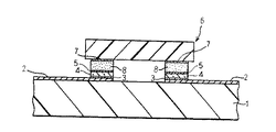
図1は本発明の一形態に係る半導体素子の実装構造体を示す断面図、図2は図1の要部拡大図であり、1 は絶縁基板、2は回路配線、3 は亜鉛−銅めっき層、4はニッケルめっき層、5は金めっき層、6は半導体素子、7は端子、8は半田である。
【0012】
前記絶縁基板1は、アルミナセラミックス等のセラミック材料により形成されており、その上面で回路配線2やめっき層3,4,5を支持するための支持母材として機能するものである。
【0013】
前記絶縁基板1は、例えばアルミナセラミックスから成る場合、アルミナ、シリカ、マグネシア等のセラミックス原料粉末に適当な有機溶剤、溶媒を添加・混合して泥漿状に成すとともに、これを従来周知のドクターブレード法やカレンダーロール法等を採用することによってセラミックグリーンシートを得、しかる後、該セラミックグリーンシートを所定の長方形状に打ち抜いた上、高温で焼成することによって製作される。
【0014】
また前記絶縁基板1の上面には、アルミニウムから成る複数個の回路配線2が所定パターンに被着されている。
【0015】
前記回路配線2は、外部電気回路からの入力信号や外部電源からの電力を半導体素子6に供給したり、或いは、半導体素子6からの出力信号を他の電気回路等に供給したりするためのものであり、その一端で半導体素子6の対応する端子7に半田8を介して電気的に接続される。
【0016】
尚、前記回路導体2は、従来周知の薄膜手法、具体的には、スパッタリングやフォトリソグラフィー技術,エッチング技術等を採用し、アルミニウムを所定厚み、所定パターンに被着させることによって絶縁基板1の上面に形成される。
【0017】
また前記回路導体2の一部上面、具体的には後述する半導体素子6の端子7が半田接合される部位には、亜鉛−銅めっき層3、ニッケルめっき層4及び金めっき層5が順次、被着されている。
【0018】
前記亜鉛−銅めっき層3は、ニッケルめっき層4を形成する際の触媒として機能するものであり、例えば0.3μm〜0.6μmの厚みを有し、銅含有率が1wt%〜20wt%に設定される。
【0019】
かかる亜鉛−銅めっき層3は、亜鉛の中に粒径100Å〜200Å程度の小さな銅の塊を分散させた状態、もしくは亜鉛と銅とで合金をつくった状態で形成されており、従来周知の無電解めっき法を採用することによって所定厚みに被着・形成される。このとき、亜鉛−銅合金の無電解めっきに使用されるめっき液には硝酸を含有させておく必要がないことから、亜鉛−銅めっき層3の形成に伴いアルミニウムから成る回路配線2が酸化・腐食されることは殆どない。
【0020】
またこの場合、前記めっき液中にキレート剤を添加しておけば、亜鉛−銅めっき層3の厚みや組成が均一になり、良好な亜鉛−銅めっき層3を得ることができる。従って亜鉛−銅めっき層3を形成するためのめっき液にはキレート剤を添加しておくことが好ましい。
【0021】
また前記亜鉛−銅めっき層3上のニッケルめっき層4は、半導体素子6の端子7を回路配線2に半田接合する際、回路配線2の半田濡れ性を良好になして半導体素子6の端子7を回路配線2に対して確実に半田接合させるためのものであり、亜鉛−銅めっき層3の上面に例えば2μm〜5μmの厚みに被着・形成される。
【0022】
前記ニッケルめっき層4は、従来周知の無電解めっき法を採用することによって亜鉛−銅めっき層3の上面に被着・形成され、このとき、ニッケルの形成に使用されるめっき液は次亜リン酸ナトリウムを還元剤として含んでおり、かかるめっき液には亜鉛−銅めっき層3中の亜鉛が溶解することから、この溶解に伴って亜鉛−銅めっき層3の表面には径100Å〜200Åの微細孔が1000〜5000個/μm2 の密度で多数形成され、ニッケルめっき層4を多数の微細孔を有した亜鉛−銅めっき層3の上面にアンカー効果によって極めて強固に被着させることができる。従って半導体素子6の実装等に伴って熱が印加されても、ニッケルめっき層4が下地(亜鉛−銅めっき層3)より剥離するのが有効に防止され、半導体素子6を回路基板上に良好な状態で実装させておくことができる。
【0023】
ここで、亜鉛−銅めっき層3中の銅含有率が1wt%よりも小さいと微細孔の形成密度が小さくなってニッケルめっき層4を亜鉛−銅めっき層3の上面に極めて強固に被着させておくことが難しくなり、また銅含有率が20wt%よりも大きいとニッケルめっき層4の形成時にニッケルの析出速度が遅くなって所定厚みのニッケルめっき層4を得るのに長時間を要することなる。従ってニッケルめっき層4を亜鉛−銅めっき層3の上面に極めて強固に、且つ短時間で効率良く被着・析出させるには、亜鉛−銅めっき層3中の銅含有率を1wt%〜20wt%の範囲内に設定しておくことが好ましい。
【0024】
またこのとき、ニッケルめっき層4の形成に使用するめっき液中にスルフォン酸塩やスルフォンアミド等を所定量、添加・混合させておけば、ニッケルめっき層4の内部応力が圧縮応力となり、ニッケルめっき層4を亜鉛−銅めっき層3に対してより強固に被着させることが可能となる。従ってニッケルめっき層4の形成に使用するめっき液中にはスルフォン酸塩やスルフォンアミドを添加・混合させておくことが好ましい。
【0025】
更に前記ニッケルめっき層4上に被着される金めっき層5は、ニッケルめっき層4の表面が大気中の水分等によって深い領域まで酸化・腐食されてしまうのを有効に防止するためのものであり、ニッケルめっき層4の上面に例えば0.04μm〜0.05μmの厚みに被着・形成される。
【0026】
前記金めっき層5は、従来周知の無電解めっき法を採用することによってニッケルめっき層4の上面に所定厚みに被着・形成される。
【0027】
そして上述した回路基板上には、半導体素子6がフェースダウンボンディングにて実装される。
【0028】
前記半導体素子6は、単結晶シリコン等から成る基材の下面に高密度にパターン形成された電子回路と複数個の端子7とを有しており、一部の端子7を介して内部に信号が入力されると、これらの入力信号に基づいて他の端子7より所定の出力を発するようになっている。
【0029】
前記半導体素子6は、その下面に設けられている複数個の端子7が絶縁基板上面の対応する回路配線2の一端、具体的には亜鉛−銅めっき層3、ニッケルめっき層4及び金めっき層5を被着させた箇所に半田8を介して対面配置されるようにして絶縁基板1上に載置され、しかる後、半田8を加熱・溶融させて回路配線2と端子7とを半田接合することによって半導体素子6が絶縁基板1上に取着・実装されることとなる。
【0030】
尚、本発明の実装構造体は上述の形態に限定されるものではなく、本発明の要旨を逸脱しない範囲において種々の変更、改良等が可能である。
【0031】
例えば上述の形態において各めっき層3,4,5を無電解めっきによって被着させる際にその前処理として洗浄等を行っても良いことは勿論である。
【0032】
【発明の効果】
本発明によれば、アルミニウムから成る回路配線と亜鉛−銅めっき層、亜鉛−銅めっき層とニッケルめっき層がそれぞれ強固に被着されるため、半導体素子の実装等に伴って熱が印加されても、亜鉛−銅めっき層やニッケルめっき層が下地より剥離することはなく、半導体素子を回路基板上に良好な状態で実装させておくことができる。
【0033】
また本発明によれば、亜鉛−銅めっき層中の銅含有率を1wt%〜20wt%に設定しておくことにより、ニッケルめっき層を亜鉛−銅めっき層の上面に極めて強固に、且つ短時間で効率良く被着・析出させることができる。
【図面の簡単な説明】
【図1】本発明の一形態に係る半導体素子の実装構造体を示す断面図である。
【図2】図1の要部拡大図である。
【符号の説明】
1 ・・・絶縁基板、2・・・回路配線、3 ・・・亜鉛−銅めっき層、4・・・ニッケルめっき層、5・・・金めっき層、6・・・半導体素子、7・・・端子、8・・・半田[0001]
BACKGROUND OF THE INVENTION
The present invention relates to a semiconductor element mounting structure used in various electronic devices.
[0002]
[Prior art]
Conventionally, face-down bonding is known as a method for mounting a semiconductor element.
[0003]
A plurality of terminals are provided on the lower surface of the semiconductor element used for the face-down bonding in addition to the electronic circuit patterned at high density, and the plurality of terminals are connected to the corresponding circuit wiring on the upper surface of the insulating substrate. The semiconductor element is mounted on the insulating substrate by soldering to the insulating substrate.
[0004]
In addition, aluminum is generally used for the formation of the circuit wiring from the viewpoint of easiness of processing, and in this case, the upper surface of the circuit wiring to be soldered is nickel-plated to improve solder wettability. A layer and a gold plating layer were sequentially deposited.
[0005]
[Problems to be solved by the invention]
By the way, in this conventional mounting structure, palladium is usually used as a catalyst for depositing a nickel plating layer on circuit wiring made of aluminum.
[0006]
However, when palladium is used as a catalyst, the surface of the circuit wiring made of aluminum is oxidized and corroded by nitric acid in the plating solution used to form the palladium plating layer, and the adhesion between the circuit wiring and the palladium plating layer is remarkably high. It will be low. For this reason, when heat is applied to the palladium plating layer and the circuit wiring therebelow as the semiconductor element is mounted, the palladium plating layer may be peeled off from the circuit wiring due to thermal stress. However, it has a drawback that it cannot be mounted in a good state.
[0007]
On the other hand, it has been studied to use zinc as a catalyst instead of the above-mentioned palladium, and this zinc can be deposited on circuit wiring using a plating solution not containing nitric acid. The circuit wiring made of aluminum is hardly oxidized or corroded with the formation, and the galvanized layer can be firmly attached to the upper surface of the circuit wiring made of aluminum.
[0008]
However, since the galvanized layer is not so familiar with the nickel plated layer deposited on it, eventually, as with the conventional mounting structure described above, with the mounting of semiconductor elements, etc. When heat is applied to the nickel plating layer or the galvanization layer below the nickel plating layer, the nickel plating layer has a drawback that it peels off from the galvanization layer due to thermal stress.
[0009]
[Means for Solving the Problems]
The present invention has been devised in view of the above drawbacks, and a semiconductor element mounting structure according to the present invention includes an insulating substrate to which circuit wiring is attached and a semiconductor element having a plurality of terminals on the lower surface. A semiconductor element mounting structure in which the terminals of the semiconductor element are electrically connected to each other by solder bonding to the circuit wiring on the insulating substrate, wherein the circuit wiring is made of aluminum, and is connected to the solder joint of the circuit wiring. A zinc-copper plating layer, a nickel plating layer, and a gold plating layer are sequentially deposited.
[0010]
In the semiconductor element mounting structure of the present invention, the copper content in the zinc-copper plating layer is 1 wt% to 20 wt%.
[0011]
DETAILED DESCRIPTION OF THE INVENTION
Hereinafter, the present invention will be described in detail with reference to the accompanying drawings.
FIG. 1 is a cross-sectional view showing a mounting structure of a semiconductor device according to an embodiment of the present invention, FIG. 2 is an enlarged view of a main part of FIG. 1, 1 is an insulating substrate, 2 is circuit wiring, and 3 is zinc-copper plating.
[0012]
The insulating substrate 1 is made of a ceramic material such as alumina ceramics, and functions as a support base material for supporting the
[0013]
When the insulating substrate 1 is made of, for example, alumina ceramics, an appropriate organic solvent or solvent is added to and mixed with ceramic raw material powders such as alumina, silica, and magnesia to form a slurry, and this is formed by a conventionally known doctor blade method. A ceramic green sheet is obtained by employing a calender roll method or the like, and thereafter, the ceramic green sheet is punched into a predetermined rectangular shape and then fired at a high temperature.
[0014]
On the upper surface of the insulating substrate 1, a plurality of
[0015]
The
[0016]
The
[0017]
Further, a zinc-
[0018]
The zinc-
[0019]
The zinc-
[0020]
In this case, if a chelating agent is added to the plating solution, the thickness and composition of the zinc-
[0021]
Further, the
[0022]
The
[0023]
Here, when the copper content in the zinc-
[0024]
At this time, if a predetermined amount of sulfonate or sulfonamide is added and mixed in the plating solution used for forming the
[0025]
Further, the
[0026]
The
[0027]
The semiconductor element 6 is mounted on the circuit board described above by face-down bonding.
[0028]
The semiconductor element 6 has an electronic circuit and a plurality of terminals 7 which are patterned on a lower surface of a base material made of single crystal silicon or the like and a plurality of terminals 7. Is input, a predetermined output is emitted from the other terminal 7 based on these input signals.
[0029]
The semiconductor element 6 has a plurality of terminals 7 provided on the lower surface thereof, one end of the
[0030]
The mounting structure of the present invention is not limited to the above-described embodiment, and various changes and improvements can be made without departing from the gist of the present invention.
[0031]
For example, when the plating layers 3, 4, and 5 are deposited by electroless plating in the above-described embodiment, it is needless to say that washing or the like may be performed as a pretreatment.
[0032]
【The invention's effect】
According to the present invention, the circuit wiring made of aluminum and the zinc-copper plating layer, and the zinc-copper plating layer and the nickel plating layer are firmly attached, so that heat is applied along with the mounting of the semiconductor element. However, the zinc-copper plating layer and the nickel plating layer are not peeled off from the base, and the semiconductor element can be mounted on the circuit board in a good state.
[0033]
Further, according to the present invention, by setting the copper content in the zinc-copper plating layer to 1 wt% to 20 wt%, the nickel plating layer is extremely strong on the upper surface of the zinc-copper plating layer and in a short time. It is possible to deposit and deposit efficiently.
[Brief description of the drawings]
FIG. 1 is a cross-sectional view illustrating a semiconductor element mounting structure according to an embodiment of the present invention.
FIG. 2 is an enlarged view of a main part of FIG.
[Explanation of symbols]
DESCRIPTION OF SYMBOLS 1 ... Insulating substrate, 2 ... Circuit wiring, 3 ... Zinc-copper plating layer, 4 ... Nickel plating layer, 5 ... Gold plating layer, 6 ... Semiconductor element, 7 ...・ Terminal, 8 ... solder
Claims (2)
前記回路配線はアルミニウムから成り、かつ該回路配線の半田接合部に亜鉛−銅めっき層、ニッケルめっき層及び金めっき層が順次、被着させてあることを特徴とする半導体素子の実装構造体。A semiconductor comprising an insulating substrate to which circuit wiring is deposited and a semiconductor element having a plurality of terminals on the lower surface, and electrically connected by soldering the terminals of the semiconductor element to circuit wiring on the insulating substrate In the element mounting structure,
A mounting structure for a semiconductor device, wherein the circuit wiring is made of aluminum, and a zinc-copper plating layer, a nickel plating layer, and a gold plating layer are sequentially deposited on a solder joint portion of the circuit wiring.
Priority Applications (1)
| Application Number | Priority Date | Filing Date | Title |
|---|---|---|---|
| JP35941299A JP4199397B2 (en) | 1999-12-17 | 1999-12-17 | Semiconductor device mounting structure |
Applications Claiming Priority (1)
| Application Number | Priority Date | Filing Date | Title |
|---|---|---|---|
| JP35941299A JP4199397B2 (en) | 1999-12-17 | 1999-12-17 | Semiconductor device mounting structure |
Publications (2)
| Publication Number | Publication Date |
|---|---|
| JP2001176920A JP2001176920A (en) | 2001-06-29 |
| JP4199397B2 true JP4199397B2 (en) | 2008-12-17 |
Family
ID=18464379
Family Applications (1)
| Application Number | Title | Priority Date | Filing Date |
|---|---|---|---|
| JP35941299A Expired - Fee Related JP4199397B2 (en) | 1999-12-17 | 1999-12-17 | Semiconductor device mounting structure |
Country Status (1)
| Country | Link |
|---|---|
| JP (1) | JP4199397B2 (en) |
Families Citing this family (1)
| Publication number | Priority date | Publication date | Assignee | Title |
|---|---|---|---|---|
| JP2010056191A (en) * | 2008-08-27 | 2010-03-11 | Mitsubishi Electric Corp | Method of manufacturing semiconductor device, and semiconductor device |
-
1999
- 1999-12-17 JP JP35941299A patent/JP4199397B2/en not_active Expired - Fee Related
Also Published As
| Publication number | Publication date |
|---|---|
| JP2001176920A (en) | 2001-06-29 |
Similar Documents
| Publication | Publication Date | Title |
|---|---|---|
| JPS58164249A (en) | Method of selectively covering metal | |
| JP2002076189A (en) | Wiring board | |
| JP2001176920A (en) | Semiconductor element mounting structure | |
| JP4090151B2 (en) | Package substrate | |
| JP4683768B2 (en) | Wiring board | |
| JP2001024296A (en) | Ceramic circuit board | |
| JP3596335B2 (en) | Semiconductor mounting substrate using wire bonding terminals | |
| US5784779A (en) | Method for joining an electrical connection of a non-packaged IC component with a conductive strip on a substrate | |
| JPS6035543A (en) | Manufacture of semiconductor device | |
| JP3801334B2 (en) | Semiconductor device mounting substrate and manufacturing method thereof | |
| JPH05283853A (en) | Printed-circuit board | |
| JP3898482B2 (en) | Wiring board | |
| JP3554195B2 (en) | Wiring board | |
| JP2866512B2 (en) | Wiring board | |
| JP2690643B2 (en) | Wiring board | |
| JPH0465024A (en) | Jumper chip | |
| JPH10107394A (en) | Ceramic wiring board | |
| JP3740407B2 (en) | Wiring board | |
| JP4511011B2 (en) | Wiring board manufacturing method | |
| JP3645744B2 (en) | Ceramic wiring board | |
| JP2001044323A (en) | Circuit board for mounting electronic components | |
| JPS61256688A (en) | Manufacture of circuit board | |
| JP4646373B2 (en) | Wiring board and manufacturing method thereof | |
| JP2002016176A (en) | Wiring board and its connection structure | |
| JPS61245555A (en) | Terminal connecting structure for semiconductor |
Legal Events
| Date | Code | Title | Description |
|---|---|---|---|
| A621 | Written request for application examination |
Free format text: JAPANESE INTERMEDIATE CODE: A621 Effective date: 20061117 |
|
| A977 | Report on retrieval |
Free format text: JAPANESE INTERMEDIATE CODE: A971007 Effective date: 20080829 |
|
| TRDD | Decision of grant or rejection written | ||
| A01 | Written decision to grant a patent or to grant a registration (utility model) |
Free format text: JAPANESE INTERMEDIATE CODE: A01 Effective date: 20080909 |
|
| A01 | Written decision to grant a patent or to grant a registration (utility model) |
Free format text: JAPANESE INTERMEDIATE CODE: A01 |
|
| A61 | First payment of annual fees (during grant procedure) |
Free format text: JAPANESE INTERMEDIATE CODE: A61 Effective date: 20081003 |
|
| FPAY | Renewal fee payment (event date is renewal date of database) |
Free format text: PAYMENT UNTIL: 20111010 Year of fee payment: 3 |
|
| R150 | Certificate of patent or registration of utility model |
Ref document number: 4199397 Country of ref document: JP Free format text: JAPANESE INTERMEDIATE CODE: R150 Free format text: JAPANESE INTERMEDIATE CODE: R150 |
|
| FPAY | Renewal fee payment (event date is renewal date of database) |
Free format text: PAYMENT UNTIL: 20121010 Year of fee payment: 4 |
|
| FPAY | Renewal fee payment (event date is renewal date of database) |
Free format text: PAYMENT UNTIL: 20131010 Year of fee payment: 5 |
|
| LAPS | Cancellation because of no payment of annual fees |