JP4177329B2 - Semiconductor processing apparatus and IC card - Google Patents
Semiconductor processing apparatus and IC card Download PDFInfo
- Publication number
- JP4177329B2 JP4177329B2 JP2004534032A JP2004534032A JP4177329B2 JP 4177329 B2 JP4177329 B2 JP 4177329B2 JP 2004534032 A JP2004534032 A JP 2004534032A JP 2004534032 A JP2004534032 A JP 2004534032A JP 4177329 B2 JP4177329 B2 JP 4177329B2
- Authority
- JP
- Japan
- Prior art keywords
- memory
- nonvolatile memory
- write
- byte
- data
- Prior art date
- Legal status (The legal status is an assumption and is not a legal conclusion. Google has not performed a legal analysis and makes no representation as to the accuracy of the status listed.)
- Expired - Fee Related
Links
Images


Classifications
-
- G—PHYSICS
- G07—CHECKING-DEVICES
- G07F—COIN-FREED OR LIKE APPARATUS
- G07F7/00—Mechanisms actuated by objects other than coins to free or to actuate vending, hiring, coin or paper currency dispensing or refunding apparatus
- G07F7/08—Mechanisms actuated by objects other than coins to free or to actuate vending, hiring, coin or paper currency dispensing or refunding apparatus by coded identity card or credit card or other personal identification means
- G07F7/10—Mechanisms actuated by objects other than coins to free or to actuate vending, hiring, coin or paper currency dispensing or refunding apparatus by coded identity card or credit card or other personal identification means together with a coded signal, e.g. in the form of personal identification information, like personal identification number [PIN] or biometric data
- G07F7/1008—Active credit-cards provided with means to personalise their use, e.g. with PIN-introduction/comparison system
-
- G—PHYSICS
- G06—COMPUTING; CALCULATING OR COUNTING
- G06Q—INFORMATION AND COMMUNICATION TECHNOLOGY [ICT] SPECIALLY ADAPTED FOR ADMINISTRATIVE, COMMERCIAL, FINANCIAL, MANAGERIAL OR SUPERVISORY PURPOSES; SYSTEMS OR METHODS SPECIALLY ADAPTED FOR ADMINISTRATIVE, COMMERCIAL, FINANCIAL, MANAGERIAL OR SUPERVISORY PURPOSES, NOT OTHERWISE PROVIDED FOR
- G06Q20/00—Payment architectures, schemes or protocols
- G06Q20/30—Payment architectures, schemes or protocols characterised by the use of specific devices or networks
- G06Q20/34—Payment architectures, schemes or protocols characterised by the use of specific devices or networks using cards, e.g. integrated circuit [IC] cards or magnetic cards
- G06Q20/341—Active cards, i.e. cards including their own processing means, e.g. including an IC or chip
-
- G—PHYSICS
- G06—COMPUTING; CALCULATING OR COUNTING
- G06Q—INFORMATION AND COMMUNICATION TECHNOLOGY [ICT] SPECIALLY ADAPTED FOR ADMINISTRATIVE, COMMERCIAL, FINANCIAL, MANAGERIAL OR SUPERVISORY PURPOSES; SYSTEMS OR METHODS SPECIALLY ADAPTED FOR ADMINISTRATIVE, COMMERCIAL, FINANCIAL, MANAGERIAL OR SUPERVISORY PURPOSES, NOT OTHERWISE PROVIDED FOR
- G06Q20/00—Payment architectures, schemes or protocols
- G06Q20/38—Payment protocols; Details thereof
- G06Q20/40—Authorisation, e.g. identification of payer or payee, verification of customer or shop credentials; Review and approval of payers, e.g. check credit lines or negative lists
- G06Q20/409—Device specific authentication in transaction processing
- G06Q20/4097—Device specific authentication in transaction processing using mutual authentication between devices and transaction partners
- G06Q20/40975—Device specific authentication in transaction processing using mutual authentication between devices and transaction partners using encryption therefor
-
- G—PHYSICS
- G07—CHECKING-DEVICES
- G07F—COIN-FREED OR LIKE APPARATUS
- G07F7/00—Mechanisms actuated by objects other than coins to free or to actuate vending, hiring, coin or paper currency dispensing or refunding apparatus
- G07F7/08—Mechanisms actuated by objects other than coins to free or to actuate vending, hiring, coin or paper currency dispensing or refunding apparatus by coded identity card or credit card or other personal identification means
- G07F7/0806—Details of the card
- G07F7/0833—Card having specific functional components
- G07F7/084—Additional components relating to data transfer and storing, e.g. error detection, self-diagnosis
-
- G—PHYSICS
- G11—INFORMATION STORAGE
- G11C—STATIC STORES
- G11C11/00—Digital stores characterised by the use of particular electric or magnetic storage elements; Storage elements therefor
- G11C11/005—Digital stores characterised by the use of particular electric or magnetic storage elements; Storage elements therefor comprising combined but independently operative RAM-ROM, RAM-PROM, RAM-EPROM cells
-
- G—PHYSICS
- G11—INFORMATION STORAGE
- G11C—STATIC STORES
- G11C16/00—Erasable programmable read-only memories
- G11C16/02—Erasable programmable read-only memories electrically programmable
- G11C16/04—Erasable programmable read-only memories electrically programmable using variable threshold transistors, e.g. FAMOS
- G11C16/0408—Erasable programmable read-only memories electrically programmable using variable threshold transistors, e.g. FAMOS comprising cells containing floating gate transistors
- G11C16/0425—Erasable programmable read-only memories electrically programmable using variable threshold transistors, e.g. FAMOS comprising cells containing floating gate transistors comprising cells containing a merged floating gate and select transistor
-
- G—PHYSICS
- G11—INFORMATION STORAGE
- G11C—STATIC STORES
- G11C16/00—Erasable programmable read-only memories
- G11C16/02—Erasable programmable read-only memories electrically programmable
- G11C16/04—Erasable programmable read-only memories electrically programmable using variable threshold transistors, e.g. FAMOS
- G11C16/0408—Erasable programmable read-only memories electrically programmable using variable threshold transistors, e.g. FAMOS comprising cells containing floating gate transistors
- G11C16/0433—Erasable programmable read-only memories electrically programmable using variable threshold transistors, e.g. FAMOS comprising cells containing floating gate transistors comprising cells containing a single floating gate transistor and one or more separate select transistors
-
- G—PHYSICS
- G11—INFORMATION STORAGE
- G11C—STATIC STORES
- G11C16/00—Erasable programmable read-only memories
- G11C16/02—Erasable programmable read-only memories electrically programmable
- G11C16/06—Auxiliary circuits, e.g. for writing into memory
- G11C16/10—Programming or data input circuits
- G11C16/14—Circuits for erasing electrically, e.g. erase voltage switching circuits
- G11C16/16—Circuits for erasing electrically, e.g. erase voltage switching circuits for erasing blocks, e.g. arrays, words, groups
Description
本発明は、ICカード用マイクロコンピュータなどの半導体処理装置及びICカードに関し、例えば電気的に書き換え可能な不揮発性メモリを有するICカード用マイクロコンピュータに適用して有効な技術に関する。 The present invention relates to a semiconductor processing apparatus such as an IC card microcomputer and an IC card, and more particularly to a technique effective when applied to an IC card microcomputer having an electrically rewritable nonvolatile memory.
電気的に書き換え可能な不揮発性メモリとしてメモリブロック単位の一括消去処理及びワード線単位のページ書き込み処理などのように比較的大きな単位による書き込み処理及び消去処理を可能にするいわゆるフラッシュメモリ、或いはCPUによる演算処理単位であるバイト或いはワードなどの単位で書き込み処理や消去処理を行うことが可能なEEPROM(Electrically Erasable and Programmable Read Only Memory)などが提供されている。前記EEPROMをオンチップするマイクロコンピュータ、前記フラッシュメモリをオンチップするマイクロコンピュータが夫々提供されている。前者のマイクロコンピュータについて記載された文献の例として特開昭63−266698号公報が有る。後者のマイクロコンピュータについて記載された文献の例として特開平05−266219号公報が有る。
しかしながら、前記EEPROMをオンチップするマイクロコンピュータにあっては、CPUの動作プログラムはオンチップのマスクROMで提供され、新たなプログラムを開発するときはマスクROMで提供すべきプログラムに対するシステムデバッグなどに時間を要し、TAT(Turn Around Time)の短縮が阻まれる。
また、フラッシュメモリをオンチップするマイクロコンピュータにあっては当該フラッシュメモリをCPUのワーク領域のように利用しようとすると、消去処理の単位がCPUのデータ処理単位とは整合しない。例えばCPUのデータ転送命令でフラッシュメモリにワード単位のデータを転送して書換えを行なうことは難しい。
また、仮想マシン言語プログラムなどを用いる場合にはプログラムメモリの大容量化が必要になり、チップ占有面積の増大が余儀なくされる。バイト或いはワードなどの単位でデータの書き込み処理や消去処理を行うことが可能なEEPROMにおいてはバイト或いはワードなどの単位でメモリセルを選択するためのスイッチ素子が必要になるから、その分だけフラッシュメモリに比べてチップ占有面積が大きくなる。このようなチップ占有面積増大の要因は、例えば、曲げに対する強度などの要請からチップ面積が制限されるICカード用途では無視し難い。
本発明の目的は、データ及びプログラムの格納に利用するオンチップ不揮発性メモリの大容量化と小型化を実現できる半導体処理装置、さらにはICカードを提供することにある。
本発明の別の目的は、データ及びプログラムの格納にオンチップ不揮発性メモリを利用するとき所要の情報に対する情報記憶の信頼性を向上させて小型化を実現できる半導体処理装置、さらにはICカードを提供することにある。
本発明の上記並びにその他の目的と新規な特徴は本明細書の以下の記述と添付図面から明らかにされるであろう。As an electrically rewritable non-volatile memory, a so-called flash memory or CPU that enables writing and erasing processing in relatively large units such as batch erasing processing in units of memory blocks and page writing processing in units of word lines There is provided an EEPROM (Electrically Erasable and Programmable Read Only Memory) capable of performing a writing process or an erasing process in units of operation units such as bytes or words. There are provided a microcomputer for on-chip the EEPROM and a microcomputer for on-chip the flash memory. As an example of a document describing the former microcomputer, there is JP-A-63-266698. As an example of a document describing the latter microcomputer, there is JP-A-05-266219.
However, in the microcomputer on-chip the EEPROM, the CPU operation program is provided by the on-chip mask ROM, and when developing a new program, it takes time to perform system debugging for the program to be provided by the mask ROM. Therefore, shortening of TAT (Turn Around Time) is prevented.
Further, in a microcomputer on-chip a flash memory, if the flash memory is used as a work area of the CPU, the unit of erasure processing does not match the data processing unit of the CPU. For example, it is difficult to rewrite data in units of words by transferring data to a flash memory using a CPU data transfer instruction.
Further, when using a virtual machine language program or the like, it is necessary to increase the capacity of the program memory, which inevitably increases the chip occupation area. In an EEPROM capable of performing data write processing and erase processing in units of bytes or words, a switch element for selecting a memory cell in units of bytes or words is necessary. The chip occupation area is larger than Such a factor of increasing the occupied area of the chip is difficult to ignore in an IC card application in which the chip area is limited due to, for example, a demand for strength against bending.
An object of the present invention is to provide a semiconductor processing apparatus and an IC card that can realize a large capacity and a small size of an on-chip nonvolatile memory used for storing data and programs.
Another object of the present invention is to improve the reliability of information storage for required information when using an on-chip non-volatile memory for storing data and programs, and to further reduce the size of the semiconductor processing apparatus and IC card. It is to provide.
The above and other objects and novel features of the present invention will become apparent from the following description of the present specification and the accompanying drawings.
〔1〕本発明に係る半導体処理装置は、第1データ長単位に記憶情報の消去が行われる第1の不揮発性メモリと、第2データ長単位に記憶情報の消去が行われる第2の不揮発性メモリと、中央処理装置とを有し、外部と暗号化したデータの入出力が可能である。前記第1の不揮発性メモリは前記データの暗号化に使用する暗号化鍵の格納に使用される。前記第2の不揮発性メモリは前記中央処理装置が処理すべきプログラムの格納に使用される。プログラムの格納と暗号鍵の格納に利用する不揮発性メモリを分け、夫々の不揮発性メモリに対する記憶情報の消去単位のデータ長が別々に規定されるから、プログラムの書き込み処理を行なう前の記憶情報の消去を効率化でき、CPUの演算処理で利用する暗号鍵等の書き込みにおいては必要な処理単位のデータ長(例えば8ビット)に合わせて記憶情報の消去を行なうことができる。前記処理単位のデータ長毎にメモリセルを分離するスイッチ素子はプログラム格納用の第2の不揮性メモリには不要である。この点において、プログラムを格納するような大容量を要する第2の不揮性メモリの回路規模の縮小が実現される。第1の不揮発性メモリにプログラムとデータの双方を格納する場合に比べて、半導体処理装置にオンチップされる不揮発性メモリの小型化を達成でき、その分記憶容量を増やすことが可能になる。
本発明の具体的な態様として、前記第1の不揮発性メモリは更に個人を特定するために用いられる第1データ長の情報の格納に使用することができる。
本発明の望ましい形態では、上記より明らかなように、前記第1データ長は前記第2データ長よりも短い方がよい。
本発明の更に具体的な態様として、前記半導体処理装置は外部との入出力に用いられる端子を有し、前記プログラムは前記端子を介して外部から供給され前記第2の不揮発性メモリに格納されるようにするのが望ましい。前記端子を介して容易にプログラムを格納することが可能になる。
データ処理の効率化を考慮すれば、前記中央処理装置は前記第1の不揮発性メモリと前記第2の不揮発性メモリとを並行してアクセス処理可能であるのがよい。
不揮発性メモリによるチップ占有面積面を更に低減することを考慮する。すなわち、前記第1の不揮発性メモリは複数のメモリセルから成るメモリアレイ部と選択されたメモリセルへのアクセス制御を行なう制御部とを有し、前記第2の不揮発性メモリは複数のメモリセルから成るメモリアレイ部と選択されたメモリセルへのアクセス制御を行なう制御部とを有し、このとき、前記第1の不揮発性メモリの制御部と前記第2の不揮発性メモリの制御部は少なくとも一部において共通であるのがよい。
具体的な態様として、前記共通とされる制御部の一部は、メモリセルからデータを読み出す際の読み出し信号を増幅するために用いられるアンプ回路である。また、前記共通とされる制御部の一部は、メモリセルにアクセスする際にメモリセルに印加する電圧を発生させる電圧発生回路である。また、前記共通とされる制御部の一部は、メモリセルにアクセスする際にメモリセルを選択するデコーダ回路である。デコーダ回路を共通化する場合には、双方の不揮発性メモリにおけるメモリセルは回路構成が同一であることが望ましい。メモリセルのピッチが等しくなり、メモリセルを選択する信号線の配線ピッチ等を双方の不揮発性メモリ間で同じにできる。
〔2〕本発明に係るICカードは、第1データ長単位に記憶情報の消去が行われる第1の不揮発性メモリと、第2データ長単位に記憶情報の消去が行われる第2の不揮発性メモリと、中央処理装置と、外部とデータの入出力を行なうための端子とを合成樹脂に封入して備える。前記外部とは暗号化したデータの入出力が行われる。前記第1の不揮発性メモリは前記データの暗号化に使用する暗号化鍵の格納に使用される。前記第2の不揮発性メモリは前記中央処理装置が処理すべきプログラムの格納に使用される。上記半導体処理装置と同様に、プログラムの書き込み処理を行なう前の記憶情報の消去を効率化でき、CPUの演算処理で利用する暗号鍵等の書き込みにおいては必要な処理単位のデータ長に合わせて記憶情報の消去を行なうことができる。また、第1の不揮発性メモリにプログラムとデータの双方を格納する場合に比べて、半導体処理装置にオンチップされる不揮発性メモリの小型化を達成でき、その分記憶容量を増やすことが可能になる。
外部と非接触インタフェースを行なう場合には外部とデータの入出力を行なうためのアンテナをICカードに搭載すればよい。
前記中央処理装置、第1の不揮発性メモリ及び第2の不揮発性メモリは単一の半導体基板に形成してよい。更には、前記中央処理装置と第1の不揮発性メモリを第1の半導体基板上に形成し、前記第2の不揮発性メモリは第2の半導体基板上に形成してよい。前記第1の不揮発性メモリにはデータを格納するためにメモリセルに窒化膜を用いてもよい。窒化膜は電荷をトラップする性質を有する絶縁膜であり、導体のフローティングゲートを用いる場合に比べて記憶情報の保持性能に優れる。不揮発性メモリのメモリセルにフローティングゲートを用いることは妨げない。
〔3〕別の観点による本発明の半導体処理装置は、第1データ長単位に記憶情報の消去が行われる第1の不揮発性メモリと、第2データ長単位に記憶情報の消去が行われる第2の不揮発性メモリと、中央処理装置とを有し、外部とは暗号化したデータの入出力が可能である。前記第1の不揮発性メモリと第2の不揮発性メモリは夫々複数のメモリセルを有する。夫々のメモリセルはソース領域、ドレイン領域、及び前記ソース領域とドレイン領域の間のチャネル領域を有し、前記チャネル領域上部に絶縁層を介してデータ蓄積性絶縁層と第1ゲートとを有し、前記データ蓄積性絶縁層上部に第2ゲートを有する。前記第1の不揮発性メモリと第2の不揮発性メモリはそれぞれ複数の第1ワード線を有し、第1の不揮発性メモリで記憶情報の消去が行われるとき上記第1ワード線に、対応するメモリセルが接続され、第2の不揮発性メモリで記憶情報の消去が行われるとき上記第1ワード線に、対応するメモリセルが接続され、第1の不揮発性メモリにおいて上記第1ワード線に接続されるメモリセルの数は、第2の不揮発性メモリにおいて上記第1ワード線に接続されるメモリセルの数よりも少ない。これによれば、第1不揮発性メモリに対する記憶情報の消去単位のデータ長は第2不揮発性メモリに対する記憶情報の消去単位のデータ長よりも短い。したがって、プログラムの格納とデータの格納に利用する不揮発性メモリを分け、夫々の不揮発性メモリに対して記憶情報の消去を行なうときの単位データ長が別々に規定されるから、プログラムの書き込み処理を行なう前の記憶情報の消去を効率化でき、CPUの演算処理で利用する暗号鍵などの書き込み処理においては必要な処理単位のデータ長に合わせて記憶情報の消去を行なうことができる。必要な処理単位のデータ長毎にメモリセルを分離するスイッチ素子はプログラム格納用の第2の不揮性メモリには不要である。この点において、プログラムを格納するような大容量を要する第2の不揮性メモリの回路規模の縮小が実現される。第1の不揮発性メモリにプログラムとデータの双方を格納する場合に比べて、半導体処理装置にオンチップされる不揮発性メモリの小型化を達成でき、その分記憶容量を増やすことが可能になる。更に双方の不揮発性メモリのメモリセルにはデータ蓄積性絶縁層を採用するから記憶情報の保持性能に優れ、また、データ蓄積性絶縁層には第1ゲートで制御される電流によるホットエレクトロンの注入で書込みを行なうことも可能になる。
本発明の具体的な態様として、前記第1ワード線と同数の第2ワード線を有し、前記第1ワード線は夫々のメモリセルの第2ゲートに接続され、前記第2ワード線は夫々のメモリセルの第1ゲートに接続される。また、前記第1の不揮発性メモリにおいて、記憶情報の消去が行われるとき、記憶情報の消去対象とする一部のメモリセルの第2ゲートを第1ワード線に接続可能にするスイッチ素子を有する。このスイッチ素子が記憶情報消去のデータ長単位にメモリセルを分離するスイッチを実現する。前記スイッチ素子は不揮発性メモリセルと同一導電型のMOSトランジスタである。導電型が異なる場合にはウェル領域に前記スイッチ素子を形成しなければならないからチップ占有面積が増大する。
〔4〕更に別の観点による本発明の半導体処理装置は、第1データ長単位に記憶情報の消去が行われる第1の不揮発性メモリと、第2データ長単位に記憶情報の消去が行われる第2の不揮発性メモリと、中央処理装置と、外部インタフェース回路とを有する。前記第1の不揮発性メモリはデータの格納に使用され、前記第2の不揮発性メモリは前記中央処理装置が処理すべきプログラムの格納に使用され、前記第1データ長は前記第2データ長よりも短い。上記同様に、プログラムの書き込み処理を行なう前の記憶情報の消去を効率化でき、CPUの演算処理で利用する暗号鍵などの書き込み処理においては必要な処理単位のデータ長に合わせて記憶情報の消去を行なうことができる。また、第1の不揮発性メモリにプログラムとデータの双方を格納する場合に比べて、半導体処理装置にオンチップされる不揮発性メモリの小型化を達成でき、その分記憶容量を増やすことが可能になる。
本発明の具体的な態様として、前記不揮発性メモリセルは、半導体基板に、ソース領域、ドレイン領域、及び前記ソース領域とドレイン領域に挟まれたチャンネル領域とを有し、前記チャネル領域上には、第1絶縁膜を介して配置されたコントロールゲート電極と、第2絶縁膜及び電荷蓄積性絶縁膜を介して配置され前記コントロールゲート電極と電気的に分離されたメモリゲート電極とを有し、前記コントロールゲート電極のゲート耐圧は前記メモリゲート電極のゲート耐圧よりも低い。例えば、前記コントロールゲート電極のゲート耐圧は前記CPUに含まれるMOSトランジスタのゲート耐圧に等しい。
前記コントロールゲート電極を有する選択用のMOSトランジスタ部に対しては、相対的に低い絶縁耐圧故に、比較的低いゲート電圧で比較的大きなGm(相互コンダクタンス)を得ることが容易になり、不揮発性メモリセルからの読み出し電流に対してGmを相対的に大きくする事ができ、読み出し速度の高速化に寄与する。
不揮発性メモリセルの前記メモリゲートから見た閾値電圧を比較的高く設定するには、例えばメモリゲート電極に高電圧を印加し、コントロールゲート電極側をオン状態にしてソース線からビット線に電流を流し、コントロールゲート電極側の電荷蓄積領域近傍で発生したエレクトロンを電荷蓄積領域に保持させればよい。逆に比較的低い閾値電圧を設定するには、例えば、メモリゲート電極に高電圧を印加し、コントロールゲート電極側をオン状態にしてビット線接続電極及びソース線接続電極を回路の接地電位とし、電荷蓄積領域に保持されているエレクトロンをメモリゲート電極に放出させればよい。したがって、不揮発性メモリセルに比較的低い閾値電圧又は比較的高い閾値電圧を設定する動作は、コントロールゲート制御線やビット線に高電圧を印加することなく実現することが可能である。このことは、コントロールゲート電極側のゲート耐圧が比較的低くてよいことを保証する。
本発明の具体的な態様として、第1の不揮発性メモリは第1データ長単位に記憶情報の消去が行なわれたメモリセルに対する情報保持を第1データ長単位に行なう。第2の不揮発性メモリは第2データ長単位に記憶情報の消去が行なわれたメモリセルに対する情報保持を第2データ長よりも短い単位で行なう。
〔5〕更に別の観点による本発明のICカードは、第1データ長単位に記憶情報の消去が行われる第1の不揮発性メモリと、第2データ長単位に記憶情報の消去が行われる第2の不揮発性メモリと、中央処理装置と、外部とデータの入出力を行うための端子とを合成樹脂に封入して備える。前記第1の不揮発性メモリはデータの格納に使用される。前記第2の不揮発性メモリは前記中央処理装置が処理すべきプログラムの格納に使用される。前記第1データ長は前記第2データ長よりも短い。前記外部とデータの入出力を行うための端子と共に、或は前記端子に代えて、外部とデータの入出力を行なうためのアンテナを備えて良い。
不揮発性メモリセルとして前記選択トランジスタ部とメモリセルトランジスタ部から成り選択トランジスタ部の絶縁耐圧がメモリセルトランジスタ部の絶縁耐圧よりも低くされたメモリセル構造を採用してよい。
〔6〕更に別の観点による本発明の半導体処理装置は、前記CPUを省いて第1の不揮発性メモリと第2の不揮発性メモリとを主体に上述同様に構成される。[1] A semiconductor processing apparatus according to the present invention includes a first nonvolatile memory in which stored information is erased in first data length units, and a second nonvolatile memory in which stored information is erased in second data length units. A memory and a central processing unit, and can input / output encrypted data to / from the outside. The first nonvolatile memory is used to store an encryption key used for encrypting the data. The second nonvolatile memory is used for storing a program to be processed by the central processing unit. The nonvolatile memory used for storing the program and the encryption key is divided, and the data length of the erasure unit of the stored information for each nonvolatile memory is separately defined. Therefore, the storage information before the program writing process is performed. Erasure can be made more efficient, and stored information can be erased in accordance with the data length (for example, 8 bits) of a necessary processing unit when writing an encryption key or the like used in the arithmetic processing of the CPU. The switch element for separating the memory cells for each data length of the processing unit is not necessary for the second nonvolatile memory for storing programs. In this respect, the circuit scale of the second non-volatile memory requiring a large capacity for storing the program can be reduced. Compared with the case where both the program and data are stored in the first nonvolatile memory, it is possible to reduce the size of the nonvolatile memory that is on-chip in the semiconductor processing device, and to increase the storage capacity accordingly.
As a specific aspect of the present invention, the first nonvolatile memory can be used for storing information of a first data length used for further identifying an individual.
In a desirable mode of the present invention, as apparent from the above, it is preferable that the first data length is shorter than the second data length.
As a more specific aspect of the present invention, the semiconductor processing apparatus has a terminal used for input / output with the outside, and the program is supplied from the outside through the terminal and stored in the second nonvolatile memory. It is desirable to do so. A program can be easily stored through the terminal.
In consideration of the efficiency of data processing, the central processing unit is preferably capable of performing access processing on the first nonvolatile memory and the second nonvolatile memory in parallel.
Consider further reducing the chip area occupied by the nonvolatile memory. That is, the first non-volatile memory has a memory array unit composed of a plurality of memory cells and a control unit for controlling access to the selected memory cell, and the second non-volatile memory includes a plurality of memory cells. And a control unit for controlling access to the selected memory cell. At this time, the control unit of the first nonvolatile memory and the control unit of the second nonvolatile memory are at least It should be common in some parts.
As a specific aspect, a part of the common control unit is an amplifier circuit used to amplify a read signal when reading data from a memory cell. In addition, a part of the common control unit is a voltage generation circuit that generates a voltage to be applied to the memory cell when accessing the memory cell. In addition, a part of the common control unit is a decoder circuit that selects a memory cell when accessing the memory cell. When the decoder circuit is shared, it is desirable that the memory cells in both nonvolatile memories have the same circuit configuration. The pitch of the memory cells becomes equal, and the wiring pitch of signal lines for selecting the memory cells can be made the same between both nonvolatile memories.
[2] The IC card according to the present invention includes a first nonvolatile memory in which stored information is erased in units of first data length, and a second nonvolatile in which stored information is erased in units of second data length. A memory, a central processing unit, and a terminal for inputting / outputting data to / from the outside are sealed in a synthetic resin. Input / output of encrypted data is performed with the outside. The first nonvolatile memory is used to store an encryption key used for encrypting the data. The second nonvolatile memory is used for storing a program to be processed by the central processing unit. As with the above semiconductor processing apparatus, it is possible to efficiently erase the stored information before performing the program writing process, and in accordance with the data length of the necessary processing unit when writing the encryption key used in the arithmetic processing of the CPU. Information can be erased. Further, as compared with the case where both the program and the data are stored in the first nonvolatile memory, it is possible to reduce the size of the nonvolatile memory on-chip in the semiconductor processing apparatus, and to increase the storage capacity accordingly. Become.
When performing a non-contact interface with the outside, an antenna for inputting / outputting data with the outside may be mounted on the IC card.
The central processing unit, the first nonvolatile memory, and the second nonvolatile memory may be formed on a single semiconductor substrate. Furthermore, the central processing unit and the first nonvolatile memory may be formed on a first semiconductor substrate, and the second nonvolatile memory may be formed on a second semiconductor substrate. In the first nonvolatile memory, a nitride film may be used for the memory cell in order to store data. The nitride film is an insulating film having a property of trapping electric charges, and is superior in retention performance of stored information as compared with the case of using a conductive floating gate. The use of a floating gate for a memory cell of a nonvolatile memory is not hindered.
[3] A semiconductor processing apparatus according to another aspect of the present invention provides a first nonvolatile memory in which stored information is erased in units of a first data length, and a first in which stored information is erased in units of a second data length. 2 has a non-volatile memory and a central processing unit, and can input / output encrypted data to / from the outside. Each of the first nonvolatile memory and the second nonvolatile memory has a plurality of memory cells. Each memory cell has a source region, a drain region, and a channel region between the source region and the drain region, and has a data storage insulating layer and a first gate via an insulating layer above the channel region. And a second gate on the data storage insulating layer. Each of the first nonvolatile memory and the second nonvolatile memory has a plurality of first word lines, and corresponds to the first word line when the stored information is erased in the first nonvolatile memory. When a memory cell is connected and the stored information is erased in the second nonvolatile memory, the corresponding memory cell is connected to the first word line, and connected to the first word line in the first nonvolatile memory. The number of memory cells to be performed is smaller than the number of memory cells connected to the first word line in the second nonvolatile memory. According to this, the data length of the erasure unit of the storage information for the first nonvolatile memory is shorter than the data length of the erasure unit of the storage information for the second nonvolatile memory. Therefore, the nonvolatile memory used for program storage and data storage is divided, and the unit data length for erasing stored information for each nonvolatile memory is separately defined. Erasure of stored information before performing can be made more efficient, and stored information can be erased in accordance with the data length of a necessary processing unit in writing processing such as an encryption key used in arithmetic processing of the CPU. A switch element that separates memory cells for each data length of a necessary processing unit is not necessary for the second nonvolatile memory for storing programs. In this respect, the circuit scale of the second non-volatile memory requiring a large capacity for storing the program can be reduced. Compared with the case where both the program and data are stored in the first nonvolatile memory, it is possible to reduce the size of the nonvolatile memory that is on-chip in the semiconductor processing device, and to increase the storage capacity accordingly. In addition, since the data storage insulating layer is employed in both nonvolatile memory cells, the storage performance of the stored information is excellent. In addition, hot electrons are injected into the data storage insulating layer by the current controlled by the first gate. It is also possible to perform writing.
As a specific aspect of the present invention, there are as many second word lines as the first word lines, the first word lines are connected to the second gates of the respective memory cells, and the second word lines are each Connected to the first gate of the memory cell. The first nonvolatile memory further includes a switching element that enables connection of the second gates of some memory cells to be erased of the stored information to the first word line when the stored information is erased. . This switch element realizes a switch for separating memory cells in units of data length for erasing stored information. The switch element is a MOS transistor having the same conductivity type as that of the nonvolatile memory cell. If the conductivity types are different, the switch element must be formed in the well region, so that the chip occupation area increases.
[4] According to still another aspect of the semiconductor processing apparatus of the present invention, the first nonvolatile memory in which stored information is erased in units of the first data length and the stored information are erased in units of the second data length. A second nonvolatile memory, a central processing unit, and an external interface circuit are included. The first nonvolatile memory is used for storing data, the second nonvolatile memory is used for storing a program to be processed by the central processing unit, and the first data length is greater than the second data length. Also short. Similar to the above, it is possible to improve the efficiency of erasing the stored information before performing the program writing process, and erasing the stored information in accordance with the data length of the necessary processing unit in the writing process such as the encryption key used in the arithmetic processing of the CPU. Can be performed. Further, as compared with the case where both the program and the data are stored in the first nonvolatile memory, it is possible to reduce the size of the nonvolatile memory on-chip in the semiconductor processing apparatus, and to increase the storage capacity accordingly. Become.
As a specific aspect of the present invention, the nonvolatile memory cell has a source region, a drain region, and a channel region sandwiched between the source region and the drain region on a semiconductor substrate, and the channel region is over the channel region. A control gate electrode disposed through the first insulating film, and a memory gate electrode disposed through the second insulating film and the charge storage insulating film and electrically separated from the control gate electrode, The gate breakdown voltage of the control gate electrode is lower than the gate breakdown voltage of the memory gate electrode. For example, the gate breakdown voltage of the control gate electrode is equal to the gate breakdown voltage of a MOS transistor included in the CPU.
For the selection MOS transistor portion having the control gate electrode, it is easy to obtain a relatively large Gm (mutual conductance) with a relatively low gate voltage because of a relatively low withstand voltage. Gm can be relatively increased with respect to the read current from the cell, which contributes to an increase in read speed.
In order to set the threshold voltage seen from the memory gate of the nonvolatile memory cell to be relatively high, for example, a high voltage is applied to the memory gate electrode, the control gate electrode side is turned on, and a current is supplied from the source line to the bit line The electrons generated near the charge accumulation region on the control gate electrode side may be held in the charge accumulation region. Conversely, in order to set a relatively low threshold voltage, for example, a high voltage is applied to the memory gate electrode, the control gate electrode side is turned on, and the bit line connection electrode and the source line connection electrode are set to the circuit ground potential. The electrons held in the charge storage region may be emitted to the memory gate electrode. Therefore, the operation of setting a relatively low threshold voltage or a relatively high threshold voltage in the nonvolatile memory cell can be realized without applying a high voltage to the control gate control line or the bit line. This ensures that the gate breakdown voltage on the control gate electrode side may be relatively low.
As a specific aspect of the present invention, the first non-volatile memory holds information in the first data length unit for the memory cell in which the stored information is erased in the first data length unit. The second non-volatile memory holds information in memory units in which stored information is erased in units of the second data length in units shorter than the second data length.
[5] An IC card according to another aspect of the present invention includes a first nonvolatile memory in which stored information is erased in units of a first data length, and a first nonvolatile memory in which stored information is erased in a second data length unit. 2 non-volatile memory, a central processing unit, and a terminal for inputting / outputting data to / from the outside are enclosed in a synthetic resin. The first nonvolatile memory is used for data storage. The second nonvolatile memory is used for storing a program to be processed by the central processing unit. The first data length is shorter than the second data length. An antenna for inputting / outputting data from / to the outside may be provided in addition to or instead of the terminal for inputting / outputting data from / to the outside.
As the nonvolatile memory cell, a memory cell structure that includes the selection transistor portion and the memory cell transistor portion and that has a withstand voltage lower than that of the memory cell transistor portion may be employed.
[6] A semiconductor processing apparatus according to another aspect of the present invention is configured in the same manner as described above mainly using a first nonvolatile memory and a second nonvolatile memory, omitting the CPU.
第1図は本発明に係る半導体処理装置の一例であるマイクロコンピュータのブロック図である。
第2図はマイクロコンピュータの別の例を示すブロック図である。
第3図はEEPROM及びフラッシュメモリに採用されている不揮発性メモリセルの構造を例示する縦断面図である。
第4図はメモリセルの読み出し、書込み処理、消去処理における電圧印加態様を例示する説明図である。
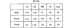
第5図はメモリセルの閾値電圧特性を例示する説明図である。
第6図はフラッシュメモリのようにバイト分割を採用しないときのメモリアレイの様子を消去処理状態を一例に示す回路図である。
第7図は第6図のメモリアレイにおける書き込み処理状態を例示する回路図である。
第8図はEEPROMのようにバイト分割を採用したときのメモリアレイの様子を消去処理状態を一例に示す回路図である。
第9図は第8図のメモリアレイにおける書き込み処理状態を例示する回路図である。
第10図は第8図のメモリアレイにおける読み出し動作状態を例示する回路図である。
第11図は第8図で説明したバイト選択トランジスタTijにpMOSトランジスタを用いたメモリアレイにおけるバイト選択トランジスタが配置されたバイト境界部分のデバイス構造平面レイアウト図である。
第12図は第11図のA−A’断面図である。
図13はバイト選択トランジスタにnMOSトランジスタを採用したときのメモリアレイの様子が消去処理状態を一例に示される回路図である。
第14図は第13図のメモリアレイにおける書き込み処理状態を例示する回路図である。
第15図は第13図のメモリアレイにおける読み出し動作状態を例示する回路図である。
第16図はバイト選択トランジスタをソース線側に設けたときのメモリアレイの様子を消去処理状態を一例に示す回路図である。
第17図は第16図のメモリアレイにおける書き込み処理状態を例示する回路図である。
第18図は第16図のメモリアレイにおける読み出し動作状態を例示する回路図である。
第19図は第16図のメモリアレイにおけるバイト選択トランジスタが配置されたバイト境界部分のデバイス構造平面レイアウト図である。
第20図は全てのメモリセルの共通ソース線側に選択トランジスタを設けたメモリアレイの様子を消去動作状態を一例に示す回路図である。
第21図は第20図のメモリアレイにおけるバイト単位の書き込み処理状態を例示する回路図である。
第22図は第20図のメモリアレイにおけるバイト単位の読み出し動作状態を例示する回路図である。
第23図は第20図のメモリアレイにおけるデバイス構造平面レイアウト図である。
第24図は不揮発性メモリモジュールのブロック図である。
第25図はフラッシュメモリを例示するブロック図である。
第26図はEEPROMを例示するブロック図である。
第27図は書き込み読み出し回路を例示するブロック図である。
第28図はセンスアンプ及び書き込み電流源の一例を示す回路図である。
第29図はセンスアンプ及び書き込み電流源の別の例を示す回路図である。
第30図はフラッシュメモリとEEPROMの並列書き込み処理を示すフローチャートである。
第31図はフラッシュメモリとEEPROMの並列的な書き込み処理及び読み出し動作を示すフローチャートである。
第32図はフラッシュメモリとEEPROMの並列的な消去処理及び読み出し動作示すフローチャートである。
第33図は第30図乃至第32図のフローチャートの処理に係るフラッシュメモリとEEPROMの主なアクセス仕様を例示する説明図である。
第34図は書き込み読み出し回路の別の例を示す回路図である。
第35図は書き込み読み出し回路の更に別の例を示す回路図である。
第36図は第35図の折り返しビット線構造のフラッシュメモリにおけるメモリセルの選択手法の一例を示す回路図である。
第37図は不揮発性メモリモジュールの別の例を示すブロック図である。
第38図はCPUのアドレス空間におけるEEPROMとフラッシュメモリのマッピングを例示する説明図である。
第39図はCPUによる消去方法の第1の例を示す説明図である。
第40図はCPUによる消去方法の第2の例を示す説明図である。
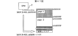
第41図はCPUによる消去方法の第3の例を示す説明図である。
第42図はCPUによる書き込み方法の第1の例を示す説明図である。
第43図はCPUによる書き込み方法の第2の例を示す説明図である。
第44図はCPUによる書き込み方法の第3の例を示す説明図である。
第45図は接触インタフェース形式のICカードの外観を例示する平面図である。
第46図は非接触インタフェース形式のICカードの外観を例示する平面図である。FIG. 1 is a block diagram of a microcomputer as an example of a semiconductor processing apparatus according to the present invention.
FIG. 2 is a block diagram showing another example of the microcomputer.
FIG. 3 is a longitudinal sectional view illustrating the structure of a nonvolatile memory cell employed in the EEPROM and flash memory.
FIG. 4 is an explanatory diagram illustrating voltage application modes in memory cell read, write, and erase processes.
FIG. 5 is an explanatory diagram illustrating the threshold voltage characteristics of the memory cell.
FIG. 6 is a circuit diagram showing an example of the erase processing state of the memory array when byte division is not adopted as in a flash memory.
FIG. 7 is a circuit diagram illustrating a write processing state in the memory array of FIG.
FIG. 8 is a circuit diagram showing an example of the erase processing state of the memory array when byte division is employed as in the case of EEPROM.
FIG. 9 is a circuit diagram illustrating a write processing state in the memory array of FIG.
FIG. 10 is a circuit diagram illustrating a read operation state in the memory array of FIG.
FIG. 11 is a device structure plan layout view of a byte boundary portion in which a byte selection transistor is arranged in a memory array using a pMOS transistor as the byte selection transistor Tij described in FIG.
FIG. 12 is a cross-sectional view taken along the line AA ′ of FIG.
FIG. 13 is a circuit diagram showing an example of the erase processing state of the memory array when an nMOS transistor is adopted as the byte selection transistor.
FIG. 14 is a circuit diagram illustrating a write processing state in the memory array of FIG.
FIG. 15 is a circuit diagram illustrating a read operation state in the memory array of FIG.
FIG. 16 is a circuit diagram showing an example of the erase processing state of the memory array when the byte selection transistor is provided on the source line side.
FIG. 17 is a circuit diagram illustrating a write processing state in the memory array of FIG.
FIG. 18 is a circuit diagram illustrating a read operation state in the memory array of FIG.
FIG. 19 is a device structure plan layout view of the byte boundary portion in which the byte selection transistors are arranged in the memory array of FIG.
FIG. 20 is a circuit diagram showing an example of an erasing operation state of a memory array in which a selection transistor is provided on the common source line side of all memory cells.
FIG. 21 is a circuit diagram illustrating a write processing state in units of bytes in the memory array of FIG.
FIG. 22 is a circuit diagram illustrating a read operation state in units of bytes in the memory array of FIG.
FIG. 23 is a plan layout view of a device structure in the memory array of FIG.
FIG. 24 is a block diagram of a nonvolatile memory module.
FIG. 25 is a block diagram illustrating a flash memory.
FIG. 26 is a block diagram illustrating an EEPROM.
FIG. 27 is a block diagram illustrating a write / read circuit.
FIG. 28 is a circuit diagram showing an example of a sense amplifier and a write current source.
FIG. 29 is a circuit diagram showing another example of the sense amplifier and the write current source.
FIG. 30 is a flowchart showing parallel writing processing of the flash memory and the EEPROM.
FIG. 31 is a flowchart showing parallel writing processing and reading operation of the flash memory and the EEPROM.
FIG. 32 is a flowchart showing parallel erase processing and read operation of the flash memory and the EEPROM.
FIG. 33 is an explanatory view exemplifying main access specifications of the flash memory and the EEPROM related to the processing of the flowcharts of FIGS.
FIG. 34 is a circuit diagram showing another example of the write / read circuit.
FIG. 35 is a circuit diagram showing still another example of the write / read circuit.
FIG. 36 is a circuit diagram showing an example of a memory cell selection method in the flash memory having the folded bit line structure of FIG.
FIG. 37 is a block diagram showing another example of a nonvolatile memory module.
FIG. 38 is an explanatory diagram illustrating the mapping between the EEPROM and the flash memory in the CPU address space.
FIG. 39 is an explanatory view showing a first example of the erasing method by the CPU.
FIG. 40 is an explanatory view showing a second example of the erasing method by the CPU.
FIG. 41 is an explanatory view showing a third example of the erasing method by the CPU.
FIG. 42 is an explanatory view showing a first example of a writing method by the CPU.
FIG. 43 is an explanatory view showing a second example of the writing method by the CPU.
FIG. 44 is an explanatory view showing a third example of the writing method by the CPU.
FIG. 45 is a plan view illustrating the appearance of a contact interface type IC card.
FIG. 46 is a plan view illustrating the appearance of a non-contact interface type IC card.
《マイクロコンピュータ》
第1図には本発明に係る半導体処理装置の一例としてマイクロコンピュータが例示される。同図に示されるマイクロコンピュータ1は、特に制限されないが、所謂ICカードマイコンと称されるマイクロコンピュータである。同図に示されるマイクロコンピュータ1は、単結晶シリコンなどの1個の半導体基板若しくは半導体チップにCMOSなどの半導体集積回路製造技術によって形成される。
マイクロコンピュータ1は、CPU2、RAM(ランダム・アクセス・メモリ)4、タイマ5、不揮発性メモリモジュール6、コプロセッサ7、クロック生成回路9、システムコントロールロジック11、入出力ポート(I/Oポート)12、データバス13、及びアドレスバス14を有する。
前記不揮発性メモリモジュール6はCPU2の動作プログラム及びデータなどを格納するのに利用される。前記RAM4はCPU2のワーク領域又はデータの一時記憶領域とされ、例えばSRAM(スタティック・ランダム・アクセス・メモリ)若しくはDRAM(ダイナミック・ランダム・アクセス・メモリ)から成る。前記CPU2は、不揮発性メモリモジュール6から命令をフェッチし、フェッチした命令をデコードし、デコード結果に基づいてオペランドフェッチやデータ演算を行う。コプロセッサ7はRSAや楕円曲線暗号演算における剰余乗算処理などをCPU2に代わって行うプロセッサユニットとされる。I/Oポート12は2ビットの入出力端子I/O1,I/O2を有し、データの入出力と外部割り込み信号の入力に兼用される。I/Oポート12はデータバス13に結合され、データバス13には前記CPU2、RAM4、タイマ5、不揮発性メモリモジュール6、及びコプロセッサ7が接続される。マイクロコンピュータ1においてCPU2がバスマスタモジュールとされ、前記RAM4、タイマ5、不揮発性メモリモジュール6、及びコプロセッサ7に接続されるアドレスバス14にアドレス信号を出力可能にされる。システムコントロールロジック11はマイクロコンピュータ1の動作モードの制御及び割り込み制御を行い、更に暗号鍵の生成に利用する乱数発生ロジックを有する。RES/はマイクロコンピュータ1に対するリセット信号である。マイクロコンピュータ1はリセット信号RES/によってリセット動作が指示されると、内部が初期化され、CPU2は不揮発性メモリモジュール6のプログラムの先頭番地から命令実行を開始する。クロック生成回路9は外部クロック信号CLKを受けて内部クロック信号CKを生成する。マイクロコンピュータ1は内部クロック信号CKに同期動作される。
特に制限されないが、前記CPU2は所謂32ビットCPUであり、32ビット(ワード)単位で演算処理が可能にされ、図示はしないが、32ビットの汎用レジスタ、32ビットの算術論理演算器などを有し、前記データバス13は32ビットとされる。したがって、CPU2の命令セットに含まれるデータ転送命令や、演算命令は、ほとんどが32ビット単位でデータを処理することができる。
前記不揮発性メモリモジュール6は、特に制限されないが、夫々電気的に消去処理及び書込み処理が可能にされるEEPROM21とフラッシュメモリ22とを有する。ここで消去処理とはメモリセルが保持する記憶情報を消去する一つの手法であり、例えばメモリセルの閾値電圧を低くする処理を意味する。この処理によって実現されるメモリセルの閾値電圧が低い状態を消去状態と称する。書き込み処理とはメモリセルに情報を保持させるための一つの手法であり、例えばメモリセルの閾値電圧を高くする処理を意味する。この処理によって実現されるメモリセルの閾値電圧が高い状態を書き込み状態と称する。EEPROM21は、第1データ長単位に記憶情報の消去が行なわれる第1の不揮発性メモリの一例であり、例えば8ビット単位で消去処理が可能にされ、書込み処理と読み出しは32ビット単位で可能にされる。フラッシュメモリ22は第2のデータ長単位に記憶情報の消去が行われる第2の不揮発性メモリの一例であり、書込みは1024ビットのようなワード線単位で行われ(ページ書込み)、消去処理は単数又は複数のワード線を単位とするブロック単位で行われ、読み出しは32ビット単位で行われる。EEPROM21は入出力データの暗号化に利用する暗号鍵、個人を特定するために用いられるID情報などの、所定の演算処理単位のデータ等を格納する領域として用いられる。ここでは所定の演算処理単位は例えば8ビット(1バイト)である。フラッシュメモリ22はCPU2が処理するプログラムの格納に利用される。例えば、仮想マシン言語プログラム、暗号化プログラム、復号プログラムなどを格納する。
プログラムの格納と暗号鍵等のデータの格納に利用する不揮発性メモリをEEPROM21とフラッシュメモリ22に分け、夫々の不揮発性メモリに対する記憶情報の消去単位のデータ長が別々に規定されるから、プログラムの書き込み処理前に行なう記憶情報の消去を効率化でき、CPU2の演算処理で利用する暗号鍵等の書き込み処理においては必要な演算処理単位のデータ長(例えば8ビット)に合わせて記憶情報の消去を行なうことができる。8ビット単位のデータ長毎にメモリセルを分離するスイッチ素子はプログラム格納用のフラッシュメモリ22には不要である。この点において、プログラムを格納するような大容量を要するフラッシュメモリ22の回路規模の縮小が実現される。EEPROMにプログラムとデータの双方を格納する場合に比べて、マイクロコンピュータにオンチップされる不揮発性メモリモジュール6の小型化を達成でき、その分記憶容量を増やすことが可能になる。第1図に示されるマイクロコンピュータ1は外部との情報入出力及び動作電源は図示を省略する電極パッド等の外部端子を介して行なう。
第2図にはマイクロコンピュータ1の別の例が示される。同図に示されるマイクロコンピュータ1は、第1図のマイクロコンピュータと外部インタフェース手段が相違される。すなわち第2図のマイクロコンピュータは図示を省略するアンテナに接続可能なアンテナ端子TML1,TML2を有する高周波部15を備える。高周波部15は前記アンテナが所定の電波(例えばマイクロ波)を横切ることによって生ずる誘導電流を動作電源として電源電圧Vccを出力し、リセット信号RES及びクロック信号CKを生成し、アンテナから非接触で情報の入出力を行なう。I/Oポートは外部と入出力すべき情報をRF部15とやり取りする。
《不揮発性メモリセル》
第3図には前記EEPROM21及びフラッシュメモリ22に採用されている不揮発性メモリセルの構造が縦断面によって例示される。ここでは、特に制限されないが、EEPROM21とフラッシュメモリ22に同じ不揮発性メモリセルを用いる。
第3図に例示される不揮発性メモリセル(単にメモリセルとも記す)MCは、シリコン基板上に設けたp型ウェル領域25に、情報記憶に用いるMOS型のメモリトランジスタ部26と、前記メモリトランジスタ部26を選択するMOS型の選択トランジスタ部27とを有して成る。メモリトランジスタ部26は、ソース線に接続するソース線接続電極としてのn型拡散層(n型不純物領域)30、電荷蓄積性絶縁膜(例えばシリコン窒化膜)31、電荷蓄積性絶縁膜31の上下に配置された絶縁膜(例えば酸化シリコン膜)32,33、及び書込み処理・消去処理時に高電圧を印加するためのメモリゲート電極(例えばn型ポリシリコン層)34を有する。例えば前記絶縁膜32は膜厚5nm、電荷蓄積性絶縁膜31は膜厚10nm(酸化シリコン膜換算)、前記絶縁膜33は膜厚3nmとされる。前記選択トランジスタ部27は、ビット線に接続するビット線接続電極としてのn型拡散層(n型不純物領域)35、ゲート絶縁膜(例えば酸化シリコン膜)36、コントロールゲート電極(例えばn型ポリシリコン層)37、前記コントロールゲート電極37とメモリゲート電極14を絶縁する絶縁膜(例えば酸化シリコン膜)38を有する。
前記メモリトランジスタ部26の電荷蓄積性絶縁膜31とその表裏に配置された絶縁膜32及び絶縁膜33(併せてONO(酸化膜・窒化膜・酸化膜)構造のメモリゲート絶縁膜となる)との膜厚の総和をtm、コントロールゲート電極37のゲート絶縁膜36の膜厚をtc、コントロールゲート電極37と電荷蓄積性絶縁膜31との間の絶縁膜38の膜厚をtiとすると、tc<tm≦tiの関係が実現されている。この絶縁膜厚さの関係より、選択トランジスタ部27のゲート絶縁耐圧はメモリトランジスタ部26のゲート絶縁耐圧よりも低くされる。
尚、拡散層35の部分に記載されたドレイン(Drain)の語はデータ読み出し動作において当該拡散層35がトランジスタのドレイン電極として機能し、拡散層30の部分に記載されたソース(Source)の語はデータ読み出し動作において当該拡散層30がトランジスタのソース電極として機能することを意味する。消去処理・書き込み処理ではドレイン電極,ソース電極の機能はドレイン(Drain),ソース(Source)の表記に対して入れ替ることがある。
第4図には前記メモリセルMCの読み出し、書込み処理、消去処理における電圧印加態様が例示される。ここで示す例は0.18μmプロセスルールで製造したメモリセルに対するものである。
メモリセルMCのメモリトランジスタ部26に比較的高い閾値電圧を設定する書き込み処理動作では、例えば、メモリゲート電圧VMGに10V、ソース線電圧VSを6Vとし、コントロールゲート電圧VCGに1.5Vを与え、書き込み状態非選択ビット線に1.5V、書き込み状態選択ビット線には1.5Vよりも低い電圧を印加して、一定の電流を流し、書き込み状態選択ビット線の選択トランジスタ部27のオン状態により、拡散層30から拡散層35にチャネル電流を流す。このチャネル電流により、コントロールゲート電極37側の電荷蓄積性絶縁膜31近傍でホットエレクトロンが発生し、このホットエレクトロンが電荷蓄積性絶縁膜31に保持される。ビット線に流す書き込み処理電流を数マイクロ・アンペア〜数十マイクロ・アンペア程度の定電流として書き込み処理を行なう場合、書き込み状態選択ビット線電位に、例えば0.8V程度印加して、チャネル電流を流せばよい。書き込み処理においては、nチャンネル型のメモリセルにとって、拡散層30がドレインとして機能し、拡散層35がソースとして機能する。この書き込み処理形式はホットエレクトロンのソースサイドインジェクションとなる。
書込み処理について更に詳述する。書き込み処理では電荷蓄積性絶縁膜31の直下に位置するチャネルはコントロールゲート電極37附近まで6Vにされ、これに対し、コントロールゲート電極37直下のチャネルは0.8V程度であり、これにより、双方のチャネルの境界部分、すなわち、コントロールゲート電極37側の電荷蓄積性絶縁膜31の直下で急峻な電界(急電界)が形成される。この急電界によりホットエレクトロンが生成され、電荷蓄積性絶縁膜31に蓄積される。コントロールゲート電極37直下のチャネルは0.8V程度であるからコントロールゲート電極37の絶縁膜32は、論理回路などの高耐圧を要しない大多数の論理動作用のMOSトランジスタと同じ又は同程度の薄膜でよい。
書き込み処理においてコントロールゲート電極37直下のチャネルが6Vにならないのは、ウェル領域25に形成される前記ビット線接続電極35とソース線接続電極30との間に高濃度不純物領域例えば拡散層が形成されていないからである。図示はしないが、記憶保持用のMONOS(メタル・オキサイド・ナイトライド・オキサイド・セミコンダクタ)型メモリトランジスタと選択用のMOSトランジスタの直列回路で構成される不揮発性メモリセルの場合には、双方のトランジスタの直列接続ノードが双方に共通の拡散領域(ソース・ドレイン領域)とされる。この双方に共通の拡散領域が介在する場合には、書き込み処理時の高電圧がMONOSに印加されてチャネルが形成されると、MONOS側の高電圧がそのチャネルから前記双方のトランジスタに共通の拡散領域を介して選択MOSトランジスタに印加される。これによって選択MOSトランジスタにも高耐圧が要求されることになる。
メモリセルMCのメモリトランジスタ部26に比較的低い閾値電圧を設定する消去処理では、例えば、メモリゲート電圧VMGに高電圧12Vを印加し、電荷蓄積性絶縁膜31に保持されているエレクトロンをメモリゲート電極34にトンネル放出させる。このとき、拡散層30を回路の接地電位(0V)とする。このとき、選択トランジスタ部27をオン状態にしてもよい。
メモリトランジスタ部26に対する上記書き込み処理・消去処理より明らかなように、コントロールゲート37の電圧VCGとビット線の電圧VDは高電圧であることを要しない。このことは、選択トランジスタ部37のゲート耐圧が比較的低くてよいことを保証する。
特に制限されないが、第5図に例示されるように、閾値電圧が低くされた消去状態のメモリトランジスタ部26はデプレション型とされ、閾値電圧が高くされた書き込み状態のメモリトランジスタ部27はエンハンスメント型とされる。第5図の消去状態・書き込み状態において、読み出し動作時におけるメモリゲート電極34は回路の接地電圧(0V)にすればよい。更に読み出し動作を高速化する場合はメモリゲート電極34に例えば電源電圧(1.5V)を印加してもよい。尚、消去及び書き込みの双方の状態をエンハンスメント型にすることは妨げない。この場合には、読み出し動作時におけるメモリゲート電極34は電源電圧を印加する。
第5図の閾値状態において第3図の不揮発性メモリセルMCに対する読み出し動作では、ソース線電圧VS、メモリゲート電圧VMGを0Vにし、読み出し選択すべきメモリセルのコントロールゲート電圧Vcgを1.5Vの選択レベルにすればよい。ビット線電位VDは1.5Vのプリチャージレベルを初期状態とする。選択トランジスタ部27がオン状態にされたときメモリトランジスタ部26の閾値電圧状態に従って電流が流れるか否かに応じてビット線に記憶情報が読み出される。選択トランジスタ部27はメモリトランジスタ部26よりもゲート絶縁膜厚が薄く、また、ゲート耐圧も小さいから、記憶保持用のMOSトランジスタ部と選択用のMOSトランジスタ部の双方を高耐圧で形成する場合に比べて、選択トランジスタ部27で得られる読み出し電流のGmを比較的に大きくする事ができ、これにより、データ読み出し速度を高速化することができる。
《バイト分割》
第6図にはフラッシュメモリのようにバイト分割を採用しないときのメモリアレイの様子が消去処理状態を一例に示される。メモリセルMCのメモリゲート電極(34)は行単位でメモリゲート制御線MG0,MG1に接続され、メモリセルMCのコントロールゲート電極(37)は行単位でコントロールゲート制御線CG0,CG1に接続される。2行分のメモリセルMCのソース線接続電極(30)は共通ソース線SL0に接続され、メモリセルMCのビット線接続電極(35)は列毎に対応するビット線b0〜b3に接続する。このメモリアレイ構成により、メモリセルMCは共通ソース線SL0側にメモリゲート電極(34)、ビット線b0〜b3側にコントロールゲート電極(37)が位置する。
消去処理は第6図に示されるようにメモリゲート制御線MG1に高圧(12V)を印加し、ビット線b0〜b3を回路の接地電位(0V)にして、電荷蓄積性絶縁膜(シリコン窒化膜)31中に蓄えられた電子をメモリゲート電極MG1に引き抜く。消去処理はメモリゲート制御線単位で行なうことができ、第6図ではメモリゲート制御線MG1を共有する一行分のメモリセルが一括消去される。
書き込み処理は第7図に例示されるように、メモリゲート制御線MG1に高圧(10V)を印加し、選択トランジスタ部(27)を導通(コントロールゲート制御線CG1=選択レベル(1.5V))させたうえで、共通ソース線SL0に高圧(6V)を印加する。書込み状態選択ビット線には選択トランジスタ部の閾電圧バラツキを補償するため、書込み電流源より所定のチャネル電流を流してソース側ホットエレクトロン注入により書き込み状態を達成する。書き込み状態非選択ビット線には1.5Vを与えて書き込み状態への遷移を抑止する。図において書き込み電流源はIsとして示される。このときの共通ソース線に印加する高圧電源による電流供給能力との関係で、一度に書き込み処理を行なうことができるメモリセルの数は往々にして消去単位に比べて小さいことが予想され、その場合には複数回に分けて直列的に書き込み処理を行なう。
前述の通り、書き込み・消去処理の時、メモリセルMCの選択トランジスタ部には高電圧が印加されないので、コントロールゲート電極の酸化膜厚を薄くでき、電流駆動能力を大きくできるので、読み出し動作は高速化される。
第8図にはEEPROMのようにバイト分割を採用したときのメモリアレイの様子が消去処理状態を一例に示される。メモリアレイの基本的な構成が第6図と同じである。相違点は、バイト分割のために、バイト毎にメモリセルMCのメモリゲート電極(34)をバイト選択トランジスタTij(i,jは整数)を介してメモリゲート制御線MGiに接続するように構成した点が相違される。バイト選択トランジスタTijのスイッチ制御信号はメモリセルのバイト列単位のバイト選択制御線BSjにて与えられる。この例ではメモリゲート制御線MGiに印加した正電圧がバイト選択トランジスタTijで電圧降下を生じないように、当該バイト選択トランジスタTijにpチャネル型MOSトランジスタ(pMOSトランジスタ)を採用する。ここでは便宜上2個のメモリセルを1バイト分のメモリセルとしている。ビット線はbj0、bj1として示される。
第8図において消去処理はバイト単位で行われる。例えばバイト選択トランジスタT10で選択される1バイトを消去対象とする。このとき、選択バイトのバイト選択制御線BS0を0V、非選択バイトのバイト選択制御線BS1を12Vとする。非選択ワードのメモリゲート制御線MG0を0V、選択ワードのメモリゲート制御線MG1を12Vとする。これにより、バイト選択トランジスタT10が導通し、選択バイトのメモリセルのメモリゲート電極(34)に消去電圧12Vが印加されて、選択バイトのメモリセルの閾値が下がって、消去状態にされる。
第9図には第8図のバイト分割を採用したメモリアレイにおける書き込み処理状態が例示される。ここでは便宜上バイト選択トランジスタT10で選択される1バイトを書き込み処理対象として図示してある。このとき、選択バイトのバイト選択制御線BS0を0Vとし、非選択バイトのバイト選択制御線BS1を10Vとする。非選択ワードのメモリゲート制御線MG0を0V、選択ワードのメモリゲート制御線MG1を10Vとすると、バイト選択トランジスタT10が導通し、選択バイトのメモリセルのメモリゲート電極(34)に10Vが印加される。更に非選択ワードのコントロールゲート制御線CG0を0V、選択ワードのコントロールゲート制御線CG1を1.5V、選択ワードのソース線SL0に6Vを印加しておき、書き込み状態選択ビットのビット線b00には電流源Isを接続し、書き込み状態非選択ビットのビット線b01には1.5Vを印加する。非選択バイトのビット線も書き込み状態非選択ビット線と同様に1.5Vを印加する。これにより、書き込み状態選択ビット(書き込み選択メモリセル)の選択トランジスタ部27が導通して前記定電流源Isによってチャネル電流が流れ、ソース側(ビット線接続電極35側)から電荷蓄積性絶縁膜31にホットキャリアが注入されて、書き込み状態選択メモリセルの閾値が上がって、書込状態にされる。
書き込み処理時に、書き込み状態非選択バイトのソース線接続電極にはソース線SL0より高圧(6V)が印加されるが、メモリセルの蓄積電荷はコントロールゲート電極37側の電荷蓄積性絶縁膜(シリコン窒化膜)31にあるため、ディスターブは抑えられる。
第10図には第8図のバイト分割を採用したメモリアレイにおける読み出し動作状態が例示される。ここでは便宜上バイト選択トランジスタT10で選択される1バイトを読み出し対象として図示してある。このとき、読み出し選択バイトのビット線b00、b01を1.5Vにプリチャージしておき、選択ワードのコントロールゲート制御線CG1を1.5Vとして、読み出し選択バイトのメモリセルにおける選択トランジスタ部27を導通させる。これによるビット線の電位を図示を省略するセンスアンプで検出する。
第8図乃至第10で説明したように、スプリットゲート型のMONOS構造を有する前記メモリセルMCのメモリアレイにおいて、ワード線方向に伸びたメモリゲート電極(34)をバイト選択トランジスタTij(i,jは整数)を介してメモリゲート制御線MGiに接続するように構成し、バイト選択トランジスタTijを介してメモリゲート電極(34)に書き込み高電圧や消去高電圧を印加する。これにより、バイト単位の消去処理及び書き込み処理が可能になる。また、書込み処理と消去処理の時、選択バイトのメモリゲート電極(34)のみ書き込み高電圧や消去高電圧が印加されるので、非選択バイトにはディスターブがかからない。
第11図には、第8図で説明したバイト選択トランジスタTijにpMOSトランジスタを用いたメモリアレイにおけるバイト選択トランジスタが配置されたバイト境界部分のデバイス構造平面レイアウトが示され、第12図には第11図のA−A’断面が示される。バイト選択トランジスタTijは、pMOSトランジスタでありメモリセルとは導電型が異なるので、n型ウェル領域(Nwell)に形成される。メモリセルはp型ウェル領域(Pwell)に形成され、両方の領域は相互にアイソレーション領域によって電気的に分離されなければならず、n型ウェル領域(Nwell)には比較的大きな面積を必要とする。
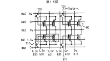
図13にはバイト選択トランジスタにnチャネル型MOSトランジスタ(nMOSトランジスタ)を採用したときのメモリアレイの様子が消去処理状態を一例に示される。メモリアレイの基本構成は第8図と同様であり、バイト選択トランジスタTijにnMOSトランジスタを採用した点が相違される。第14図には第13図のバイト分割を採用したメモリアレイにおける書き込み処理状態が例示される。第15図には第13図のバイト分割を採用したメモリアレイにおける読み出し動作状態が例示される。第13図乃至第15図において動作対象は例えばバイト選択トランジスタT10で選択される1バイトとされる。
バイト選択トランジスタTijにnMOSトランジスタを採用した場合、当該トランジスタTijによる電圧降下を補償するために、消去処理及び書き込み処理時の高電圧(昇圧電圧)は高く設定される。例えば、消去処理時には、第13図に例示されるようにメモリゲート制御線MG1への印加電圧は13Vに高く設定され、これに応じてバイト選択制御線BS0への印加電圧も13Vに高く設定される。書き込み処理時には、第14図に例示されるようにメモリゲート制御線MG1への印加電圧は11Vに高く設定され、これに応じてバイト選択制御線BS0への印加電圧も11Vに高く設定される。一方、読み出し動作時には、バイト選択トランジスタTijを導通させてメモリセルのメモリゲート電極に印加する電圧を容易に0Vにすることができる。例えば第15図では選択バイトのバイト選択制御線BS0への印加電圧を1.5Vのような電源電圧にするだけで済む。
また、第13図のメモリアレイではバイト選択トランジスタTijはnMOSトランジスタであるから、バイト境界領域の部分にNウェル領域を形成する必要がない。これにより、メモリアレイのサイズを小さくすることが可能になる。
第16図にはバイト選択トランジスタをソース線側に設けたときのメモリアレイの様子が消去処理状態を一例に示される。上述したバイト分割はバイト毎にメモリゲート電極をメモリゲート制御線から分離する構成であるのに対し、ここではバイト毎にソース線接続電極をソース線から分離可能にする。第16図では、メモリセルのバイト列毎にソース線SLjが設けられ、バイト毎にメモリセルのソース線接続電極(30)と対応するソース線との間にバイト選択トランジスタTijが挿入される。バイト選択トランジスタTijのスイッチ制御信号は行単位のバイト選択制御線BSiにて与えられる。
第16図において消去処理はバイト単位で行われる。例えばバイト選択トランジスタT10で選択される1バイトを消去対象とする。このとき、選択ワードのメモリゲート制御線MG1を12V、非選択ワードのメモリゲート制御線MG0を0Vとする。選択ワードのバイト選択制御線BS1を12Vとしてバイト選択トランジスタT1jを導通させ、非選択ワードのバイト選択制御線BS0を12Vとしてバイト選択トランジスタT0jを非導通させる。選択バイトのソース線SL0及びビット線b0jに回路の接地電圧0Vを印加し、非選択バイトのソース線SL1及びビット線b1jに消去抑止電圧12Vを印加する。これにより、選択ワードの選択バイトのメモリセルは、ゲート・基板間に高電圧が印加されて消去状態にされる。選択ワード上の非選択メモリセルはゲートと基板間に高電圧がかからず、消去状態にされない。
第17図にはバイト選択トランジスタをソース線側に設けたメモリアレイにおける書き込み処理状態が例示される。ここでは便宜上バイト選択トランジスタT10で選択される1バイトを書き込み処理対象として図示してある。このとき、選択ワードのメモリゲート制御線MG1を10V、非選択ワードのメモリゲート制御線MG0を0Vとする。選択ワードのバイト選択制御線BS1を10Vとしてバイト選択トランジスタT10を導通させ、非選択バイトのソース線SL1に書込抑止電圧10Vを印加する。これにより選択ワード上の書き込み状態非選択メモリセルにはゲートと基板間に高電圧が印加されず、ディスターブがかからない。一方、選択バイトのソース線SL0を6Vとすれば選択バイトのメモリセルのソース線接続電極(30)としてのドレインには6Vが印加される。選択バイトの書き込み状態非選択メモリセルのビット線b01はコントロールゲート制御線CG1と同電位の1.5Vとし、選択バイトの書き込み状態選択メモリセルのビット線b00には電流源Isを接続することにより、上述と同様にソース側ホットキャリア注入による書き込み状態が達成される。
第18図にはバイト選択トランジスタをソース線側に設けたメモリアレイにおける読み出し動作状態が例示される。読み出し対象は便宜上バイト選択トランジスタT10で選択される1バイトとして図示されている。第18図において選択バイトのコントロールゲート制御線CG1とバイト選択制御線BS1を3Vの選択レベルとし、選択バイトのビット線b00、b01を1.5Vにプリチャージすることにより、選択バイトのメモリセルに対する読み出しを行なうことができる。但し、読み出し電流経路には、メモリトランジスタ26に対し選択トランジスタ部27とバイト選択トランジスタTijの2個のnチャネルMOS型トランジスタが直列配置されるので、第10図及び第15図の例に比べ、CG1とBS1の選択レベルは3Vの昇圧電圧に成っている点が相違される。
第19図には第16図で説明したバイト選択トランジスタをソース線側に設けたメモリアレイにおけるバイト選択トランジスタが配置されたバイト境界部分のデバイス構造平面レイアウトが示される。バイト選択トランジスタTijはメモリセルと同じnチャンネル型であるから同じp型ウェル領域に形成できる。
第20図には全てのメモリセルの共通ソース線側に選択トランジスタを設けたメモリアレイの様子が消去動作状態を一例に示される。上述したメモリアレイはバイト毎にソース線を分離し、バイト選択トランジスタを付加したが、ここでは、一方に選択トランジスタ部27が接続されたメモリトランジスタ部26の他方にも選択トランジスタ部27aを形成し、3重ゲート構造のメモリセルMCaを採用する。このメモリセルMCaは、特に図示はしないが、第3図の断面構造においてメモリトランジスタ部26を中心に左右対称に拡散領域とコントロールゲート電極を形成し、一方の拡散領域をビット線接続電極、他方の拡散領域をソース線接続電極とすればよい。要するに、メモリゲート電極の両側にコントロールゲート電極が配置される。第20図においてコントロールゲート制御線CGia(iは整数)はビット線bj0,bj1(jは整数)に接続する選択トランジスタ部のコントロールゲートを制御し、コントロールゲート制御線CGibはソース線SLjに接続する選択トランジスタ部のコントロールゲートを制御する。コントロールゲート制御線CG0b,CG1bは第16図のメモリアレイにおけるバイト選択制御線BS0,BS1に相当する。第20図のメモリアレイにおけるバイト単位の消去処理、第21図に示されるバイト単位の書き込み処理、第22図に示されるバイト単位の読み出し動作は、第16図の消去処理、第17図の書込み処理、第18図の読み出し動作と同じである。
第23図には第20図で説明したメモリセルの共通ソース線側に選択トランジスタを設けたメモリアレイにおけるデバイス構造平面レイアウトが示される。選択トランジスタ部27aはメモリセルMCaの一部を構成し、全てのメモリセルMCaに対して規則的に配置される。第19図の場合にはバイト選択トランジスタTijを配置するために縦方向及び横方向の双方向でチップ面積を拡大している。第23図の場合選択トランジスタ部27aの数は多いが、それはメモリセル配列の中に収まるから、縦方向寸法は大きくなっても横方向寸法は拡大しない。この点において、第23図のメモリアレイ構造ではバイト境界領域の面積を第19図の例よりも縮小することができる。
《不揮発性メモリモジュール》
第24図には前記不揮発性メモリモジュール6のブロック図が例示される。不揮発性メモリモジュール6は、EEPROM21に専用の回路としてEEPROM用メモリアレイ40、ビットデコーダ・ドライバ41、及びワードデコーダ・ドライバ42を有し、また、フラッシュメモリ22に専用の回路としてフラッシュメモリ用メモリアレイ43、ビットデコーダ・ドライバ44、及びワードデコーダ・ドライバ45を有する。EEPROM21とフラッシュメモリ22は前述の通り同じスプリットゲート型MONOS構造のメモリセルを用いているから、双方に一部共通化された回路として、電源回路46、書き込み読み出し回路47、及びメモリ制御回路48を備え、周辺回路が一部共通化され、メモリモジュールの小型化、更にはマイクロコンピュータチップの縮小に寄与する。
第25図にはフラッシュメモリ22の一例が示される。メモリアレイ43は第6図で説明した基本構成を備える。メモリアレイ43は複数個の消去ブロックBLK0〜BLKnに分割され、ブロック単位でソース線SL0〜SLnが設けられる。消去ブロックBLK0〜BLKnのサイズはブロック間で同じであっても全部又は部分的に相違されていてもよい。ビット線b0〜bnは各消去ブロックBLK0〜BLKnに共通化される。コントロールゲート制御線CG及びメモリゲート制御線MGはワード(ビット線に交差するメモリセル配列方向)単位とされ、例えば消去ブロックBLK0にはコントロールゲート制御線CG0〜CGnとメモリゲート制御線MG0〜MGnが割当てられる。
ビットデコーダ・ドライバ44はアドレス信号をデコードし、そのデコード結果及び動作モードにしたがってビット線の駆動等を行なう。ワードデコーダ・ドライバ45はアドレス信号をデコードし、そのデコード結果及び動作モードにしたがってコントロールゲート制御線CG及びメモリゲート制御線MGを駆動する。消去処理におけるソース線SL0〜SLnの駆動には、特に制限されないが、ワードデコーダ・ドライバ45が兼用される。書き込み読み出し回路47は、読み出し動作においてメモリアレイから読み出されたデータを増幅して出力し、書き込み処理において書き込み状態選択ビット線に対して書き込み電流の供給等を行なう。
メモリ制御回路48はアドレス信号、データ、及び制御信号を入力し、制御信号によって消去処理、書き込み処理、又は読み出し動作が指示され、その指示に従って、ビットデコーダ・ドライバ44及びワードデコーダ・ドライバ45に必要なアドレス信号を与えると共に、必要なデコード動作をさせて、コントロールゲート制御線やメモリゲート制御線等を駆動させる。動作に必要な高電圧は電源回路46が電源電圧Vccを昇圧して形成し、これが必要な回路に供給される。このように制御される消去処理はブロック単位BLK0〜BLKnで行なわれ、消去ブロックはアドレス信号の所定上位ビットを用いたり、或は消去コマンドの消去ブロック指定データを用いて指定される。書き込み処理は、特に制限されないが、4バイト(32ビット)単位のページ書き込みとされる。書込み処理では書き込み選択ビット線に書き込み電流を供給することが必要であり、電源回路46の電流供給能力が小さい場合を考慮して、1ページの書き込み処理に対して4バイト単位で直列的な書き込み処理を行なう。読み出し動作は、特に制限されないが、データバスサイズとの関係に従って、アドレス信号で指定される32ビット単位で行なわれる。
第26図にはEEPROM21の一例が示される。メモリアレイ40は第13図で説明した基本構成を備える。メモリアレイ40は複数個のバイトユニットBYU0〜BYUiに分割され、ユニット単位でソース線SL0〜SLnが設けられる。コントロールゲート制御線CG0〜CGn及びメモリゲート制御線MG0〜MGnはワード(ビット線に交差するメモリセル配列方向)単位とされ、バイトユニットBYU0〜BYUiに共通化される。バイトユニットBYU0〜BYUiの夫々は、コントロールゲート制御線CG0〜CGn毎に前記バイト選択トランジスタT00〜Tn0を有し、バイトユニットBYU0〜BYUiに固有のバイト選択制御線BS0〜BSiを有する。更にバイトユニットBYU0〜BYUiは夫々8本のビット線bi0〜bi7を有する。
ビットデコーダ・ドライバ41はアドレス信号をデコードし、そのデコード結果及び動作モードにしたがってビット線の駆動等を行なう。ワードデコーダ・ドライバ42はアドレス信号をデコードし、そのデコード結果及び動作モードにしたがってコントロールゲート制御線CG0〜CGn及びメモリゲート制御線MG0〜MGnを駆動する。消去処理におけるソース線SL0〜SLnの駆動には、特に制限されないが、ビットデコーダ・ドライバ41が兼用される。書き込み読み出し回路47は、読み出し動作においてメモリアレイ40から読み出されたデータを増幅して出力し、書き込み処理において書き込み状態選択ビット線に対して書き込み電流の供給を行なう。
メモリ制御回路48はアドレス信号、データ、及び制御信号を入力し、制御信号によって消去処理、書き込み処理、又は読み出し動作が指示され、その指示に従って、ビットデコーダ・ドライバ41及びワードデコーダ・ドライバ42に必要なアドレス信号を与えると共に、必要なデコード動作をさせて、コントロールゲート制御線やメモリゲート制御線等を駆動させる。動作に必要な高電圧は電源回路46が電源電圧Vccを昇圧して形成し、これが必要な回路に供給される。このように制御される消去、書き込み及び読み出し処理は第13図乃至第15図で説明したようにバイト単位で行なわれる。また、書き込み処理及び読み出し処理はデータバス幅に合わせて例えば32ビット単位で行なってもよい。書き込み処理及び読み出しはデータバス幅に合わせて32ビット単位で行なわれる。4バイト未満のデータ書き込み若しくは書換えのとき、4バイト単位の書込み処理において、書き込み対象以外のデータに対しては書き込み状態非選択のデータを与えて書き込み状態への遷移をマスクすればよい。
第27図には前記書き込み読み出し回路27の一例が示される。ここでは、読出し時に必要なセンスアンプをビット線毎に配置せず、CPU等との上位インタフェースがバイト単位又は複数バイト(n×バイト)単位アクセスであるのが一般であるから、回路規模縮小の観点より、それに合わせて、読み出しに必要なセンスアンプ及び書き込みに必要な定電流源回路をn×バイトで配置される。第27図ではn=4の32ビットを一例とする。即ち、ここではフラッシュメモリ22のビット線はb0_0〜b31_63とされ、64本単位で32グループに分けられ、ビット線選択信号Sbit0〜Sbit31により各グループからスイッチSWf0〜SWf31で1本ずつ合計32本のビット線が選択可能にされる。EEPROM21のビット線はb0_0〜b31_31とされ、第26図で説明したバイトユニットBYU0〜BYUiと同様の構成を有するバイトユニットBYU毎に8本のビット線が順次割当てられ、4個のバイトユニットBYUを一単位とするブロックを単位にメモリアレイの全体が32ブロックに分けられ、ブロック選択信号Sblk0〜Sblk31によりブロック単位で32本のビット線がスイッチSWe0〜SWe31にて選択される。
スイッチSWe0〜SWe31を介して選択されたEEPROM21側の32本のビット線は、選択トランジスタMes0〜Mes31を介して対応するセンスアンプ及び書き込み電流源SA・WC0〜SA・WC31に接続される。同様に、前記スイッチSWf0〜SWf31を介して選択されたフラッシュメモリ22側の32本のビット線は、選択トランジスタMfs0〜Mfs31を介して対応するセンスアンプ及び書き込み電流源SA・WC0〜SA・WC31に接続される。選択トランジスタMes0〜Mes31はEEPROM選択信号Seepによりスイッチ制御され、選択トランジスタMfs0〜Mfs31はフラッシュメモリ選択信号Sflsによりスイッチ制御される。
前記ビット線選択信号Sbit0〜Sbit31、前記ブロック選択信号Sblk0〜Sblk31は前記ビットデコーダ・ドライバ44、41がアドレス信号をデコードして生成する。フラッシュメモリ選択信号Sfls及びEEPROM選択信号Seepはメモリ制御部48がアクセスアドレス信号と動作モードに従って生成する。第27図の例では、フラッシュメモリ22に書き込み処理又は読み出し動作が指示されたときフラッシュメモリ選択信号Sflsが選択レベルにされ、EEPROM21に書き込み処理又は読み出し動作が指示されたときEEPROM選択信号Seepが選択レベルにされる。
第28図にはセンスアンプ及び書き込み電流源SA・WC0の一例が示される。この例では、センスアンプSAはpチャンネル型MOSトランジスタMp1,Mp2と、nチャンネル型MOSトランジスタMn1,Mn2から成るスタティックラッチを主体に、pチャンネル型MOSトランジスタMp3,Mp4とnチャネル型MOSトランジスタMn3から構成される。読み出し動作の開始前にプリチャージMOSトランジスタMp4によってセンスアンプSAの入出力ノードが電源電圧Vccにプリチャージされる。その後、MOSトランジスタMp3,Mn3がオン状態にされてセンスアンプSAが増幅動作可能にされる。書き込み電流源WCは、センスアンプSAの入出力ノードと回路の接地端子との間にnチャンネル型の定電流源MOSトランジスタMn4とnチャネル型のゲートMOSトランジスタMn5が直列接続されて構成される。定電流源MOSトランジスタMn4のゲートには定電流を決定するためのバイアス電圧が印加される。ゲートMOSトランジスタMn5はラッチ回路(LAT)50のラッチデータに基づいてスイッチ制御される。ラッチ回路はラッチクロックとラッチイネーブル信号によってラッチ動作が制御される。ラッチ回路50は書き込み処理においてメモリ制御部48から供給される書き込みデータをラッチする。ラッチした書込みデータの論理値“1”は、書き込み処理において書き込み状態を選択し、書込みデータの論理値“0”は、書き込み処理において書き込み状態を非選択とする。
第28図の構成は選択MOSトランジスタMfs0とMes0との結合ノードにセンスアンプSAと書き込み定電流源WCが共通接続されているから、フラッシュメモリ22とEEPROM21の何れか一方が読み出し動作を行なっているとき、他方では消去処理をそれに並列して行なうことができても、書き込み処理を並列化することはできない。尚、図示はしないが、その他のセンスアンプ及び書き込み電流源SA・WC1〜SA・WC31も同様に構成される。
第29図にはセンスアンプ及び書き込み電流源SA・WC0の別の例が示される。この例は、フラッシュメモリ22のビット線とEEPROM21のビット線の夫々に別々に前記書き込み電流源WCを配置した構成が第28図と相違される。ラッチ回路50に対する書き込みデータのラッチ入力は選択MOSトランジスタMfs0、Mes0を経由せず双方の結合ノードに直接接続される。
第29図の構成により、フラッシュメモリ22とEEPROM21の何れか一方が読み出し動作を行なっているとき、他方では書き込み処理を並列に行なうことができる。更に、フラッシュメモリ22とEEPROM21は並列的に書き込み処理を行なうことができる。フラッシュメモリ22とEEPROM21が並列的に消去処理を行なうことができること、また、読み出し処理と消去処理を並列に行なうことができることは、第28図の場合と変わりない。
第30図乃至第32図には第29図の回路構成を採用したときのフラッシュメモリ22とEEPROM21の並列アクセス処理フローが示される。この時のフラッシュメモリ22とEEPROM21の主なアクセス仕様は例えば第33図に示されるものとする。
第30図はフラッシュメモリ22とEEPROM21の並列書き込み処理フローを示す。選択MOSトランジスタMfs0〜Mfs31、Mes0〜Mes31を共にオフ状態とし(S1)、フラッシュメモリ22に対する32ビットの書き込みデータをメモリ制御回路48からフラッシュメモリ22側のラッチ回路50にセットする(S2)。同様に、EEPROM21に対する32ビットの書き込みデータをメモリ制御回路48からEEPROM21側のラッチ回路50にセットする(S3)。フラッシュメモリ22とEEPROM21に対する書き込み処理方式は前述の通りホットエレクトロン方式であり、双方のメモリ21,22にホットエレクトロンを発生させるための書き込み処理高電圧を印加すると共に、フラッシュメモリ22とEEPROM21にセットされた書き込みデータにしたがって、書き込み状態選択ビットには定電流バイアスを印加する(S4)。この書き込み処理の電圧印加状態を例えば10μs(マイクロ秒)維持する(S5)。10μsの時間は製造プロセス等で変動するので、そのプロセスに応じた必要な時間を設定してよい。その後、書き込み処理の電圧印加を解除し(S6)、書き込み処理が残っていればステップS2に戻って処理を継続する。
このように、フラッシュメモリ22とEEPROM21に対して並列書き込み処理を行なうことにより、夫々別々に処理を行なう場合に比べて、処理時間を大凡半分に短縮することができる。
第31図はフラッシュメモリ22とEEPROM21の並列的な書き込み処理及び読み出し動作のフローを示す。選択MOSトランジスタMfs0〜Mfs31、Mes0〜Mes31を共にオフ状態とし(S11)、フラッシュメモリ22又はEEPROM21の一方を書き込み処理対象とし、32ビットの書き込みデータをメモリ制御回路48から書き込み処理対象側のラッチ回路50にセットする(S12)。フラッシュメモリ22とEEPROM21に対する書き込み処理方式は前述の通りホットエレクトロン方式であり、書き込み処理対象にホットエレクトロンを発生させるための書き込み処理高電圧を印加すると共に、セットされた書き込みデータにしたがって、書き込み状態選択ビットには定電流バイアスを印加する(S13)。この書き込み処理の電圧印加状態を例えば10μs維持する(S14)。この間に、他方の読み出し対象に対しては選択MOSトランジスタをオン状態として(S15)、読み出し動作を行なう(S16)。その後、書き込み処理の電圧印加を解除し(S17)、書き込み処理が残っていればステップS11に戻って処理を継続する。
第31図の並列処理によれば、例えばフラッシュメモリ22にアプリケーションプログラム等がある場合には、EEPROM21が書き込み処理を実行中に、アプリケーションプログラム等をCPU2に実行させることができ、ソフトウェア処理速度もしくはプログラム実行処理速度の高速化に寄与するすることができる。
第32図はフラッシュメモリ22とEEPROM21の並列的な消去処理及び読み出し動作のフローを示す。選択MOSトランジスタMfs0〜Mfs31、Mes0〜Mes31を共にオフ状態とし(S21)、フラッシュメモリ22又はEEPROM21の何れか一方を消去処理対象とし、消去処理対象に消去処理に必要な高電圧を印加する(S22)。この消去処理の電圧印加状態は、フラッシュメモリ22の場合には100ms(ミリ秒)、EEPROM21の場合には1ms維持する(S23)。この間に、他方の読み出し対象に対しては選択MOSトランジスタをオン状態として(S24)、読み出し動作を行なう(S25)。その後、消去処理の電圧印加を解除し(S26)、書き込み処理が残っていればステップS21に戻って処理を継続する。
第32図の並列処理によれば、EEPROM21に通常の消去処理を実行させている1msの間、フラッシュメモリ22に対して読み出し動作を行うことができる。同様に、フラッシュメモリ22に通常の消去処理を実行させている100msの間、EEPROM21に対して読み出し動作を行うことができる。例えばフラッシュメモリ22にアプリケーションソフトウェアが格納されている場合に、EEPROM21が消去処理を実行中に、CPU2にそのアプリケーションソフトウェアを実行させることができ、ソフトウェアの実行処理速度の高速化を図ることができる。
尚、消去処理時間もプロセス等で変動するのでその影響を考慮して消去処理時間を設定することになる。また、特に図示はしないが、並列消去処理、消去処理と書き込み処理の並列化についても容易に行なうことが可能である。
第34図には前記書き込み読み出し回路27の別の例が示される。第27図ではスタティックラッチをシングルエンドで利用してセンスアンプSAを構成したが、第34図ではセンスアンプ及び書き込み電流源SA・WC0〜SA・WC31に含まれるセンスアンプSAを差動型とする。第34図ではオープン・ビット線アーキテクチャ(Open−bit−line architecture)を使用する。したがって、フラッシュメモリ22を読み出し動作させるとき、センスアンプにおける基準となるビット線電位(参照電位)はEEPROM21のビット線を利用する。逆に、EEPROM21を読み出し動作させるとき、センスアンプにおける基準となるビット線電位(参照電位)はフラッシュメモリ22のビット線を利用する。前記基準ビット線電位若しくは参照電位はビット線プリチャージ動作などを利用して設定することができる。
この方式は、差動型センスアンプを使用することにより、第27図のシングルエンド型センスアンプの構成よりも読み出し動作速度の高速化が期待できる。但し、基準となるビット線電位を、読み出し対象メモリ以外のメモリのビット線から設定するため、双方のメモリ21,22のビット線容量と抵抗が同等になるようにレイアウトする必要がある。また、読み出し動作を行なう場合、フラッシュメモリ22及びEEPROM21共にビット線を使用する為、片方が読み出し動作を行なっている間、もう一方で消去処理や書き込み処理を並列的に行なうことはできない。
第35図には前記書き込み読み出し回路27の更に別の例が示される。ここでは差動型センスアンプを使用した折返しビット線アーキテクチャ(folded−bit−line architecture)を採用する。この構成において基準電位(参照電位)を与える基準ビット線は、同じメモリ内のビット線(同種のメモリビット線)を使用するようになっている。要するに、フラッシュメモリ22では64本毎のビット線のブロック毎に、下位32本のグループを一方の差動入出力、上位32本のグループを他方の差動入出力に割当てている。EEPROM21ではビット線b0_0〜b31_31の夫々を相補信号に変換してセンスアンプの差動入出力端子に接続可能にしている。相補信号への変換は、特に制限されないが、スイッチSWによる選択動作と併せて行なう。
第35図の構成により、第34図のオープン・ビット線アーキテクチャでの不都合を解消することができる。すなわち、同種のメモリ(読み出し対象メモリ)から基準ビット線電位を設定するので、フラッシュメモリ22とEEPROM21でビット線容量及び抵抗が違ってもよく、この点においてモジュールのレイアウトを気にする必要がなくなる。また、読み出し動作時においても読み出し対象メモリのビット線しか使用しないので、読み出し動作に並行して消去処理や書き込み処理を行なうことも可能になる。
第36図には第35図の前記折り返しビット線構造のフラッシュメモリ22におけるメモリセルの選択手法の一例が示される。ここでは主・副ビット線構造が採用され、副ビット線SBIT1,SBIT2は選択MOSトランジスタM1,M2によって選択的に主ビット線MBITに接続可能にされる。選択MOSトランジスタM1,M2は副ビット線選択信号SBSの非反転及び反転信号にて選択される。特に、副ビット線選択信号SBSの非反転信号及び反転信号の信号配線は途中で交差され、スイッチSW0〜SW31までの主ビット線の選択MOSトランジスタM1,M2に対するスイッチ状態と、スイッチSW0〜SW31までの主ビット線の選択MOSトランジスタM1,M2に対するスイッチ状態とは逆にされる。これにより、センスアンプSAで差動増幅を行なうとき、選択ブロックにおける副ビット線選択と参照ブロック(基準ブロック)における副ビット線選択とを行なうことができる。
第37図には不揮発性メモリモジュールの別の例が示される。同図に示される不揮発性メモリモジュール6は、フラッシュメモリ22とEEPROM21との間の共通化回路を、ワードデコーダ・ドライバ50、メモリ制御部48、電源部46とする。51,52はEEPROM21とフラッシュメモリ22用に夫々個別化された書き込み読み出し回路である。このようにワードデコーダ・ドライバ50を共通化した場合、書き込み読み出し回路51,52を個別化して、EEPROM21とフラッシュメモリ22の夫々に固有のセンスアンプを採用することができる。したがって、フラッシュメモリ22とEEPROM21で読出し速度を変えることが可能となり、例えばソフトウェアをフラッシュメモリ22に格納した場合など、フラッシュメモリ22用のセンスアンプを高速用として、ソフトウェア処理を高速化することが可能となる。
《メモリモジュールの利用形態》
前記不揮発性メモリモジュール6の利用形態について説明する。EEPROM21には暗号鍵、ユーザの個人情報などのように長期にデータ保持の必要な小サイズのデータを格納する領域に使用するのに好適である。フラッシュメモリ22には大容量かつ高速書き込みが必要なプログラムなどの情報を格納するのに好適である。EEPREOM21とフラッシュメモリ22の双方に用いるメモリセルは同一プロセスのものを用いるのがよい。共通プロセスを使用するため、マスク枚数を低減可能になるからである。電源回路46、ワードデコーダ・ドライバ50、書き込み読み出し回路47等を共通化することで、モジュール面積が低減される。またバスインターフェイスを共通化することで、チップ設計を容易化することができる。
ICカード用マイクロコンピュータに代表されるように、CPU搭載のSOC(システム・オン・チップ)に不揮発性メモリモジュール6を実装した場合、フラッシュメモリ22とEEPROM21とで記憶する情報の用途を区別する。例えばフラッシュメモリ22には、大容量という特徴を活かして仮想マシン言語によるプログラムを格納する用途等に利用する。またEEPROM21は、データ保持の高信頼性という特徴を活かして、認証用データ、個人情報などを格納する用途に利用する。
第38図にはCPU2のアドレス空間におけるEEPROM21とフラッシュメモリ22のマッピング例が示される。フラッシュメモリ22はアドレスエリアE1(例えば256KB(キロバイト))にマッピングされ、EEPROM21はそれとは異なるアドレスエリアE2(例えば64KB)にマッピングされる。この例では、アドレスエリアE1,E2のアドレス信号の下位16ビットは共通化されている。
第39図にはCPU2による消去方法の第1の例が示される。ここでは、CPU2が消去専用コマンドを発行する。消去処理の指示はコマンドコードで与える。消去対象領域、例えばフラッシュメモリの消去対象ページ、或はEEPROMにおける消去対象バイト等はコマンドオペランドとして指定する。例えば消去対象アドレスを指定する場合、例えば1ページがh’000000からh’00FFFFの64KBであるとすると、このページを消去する際に指定するアドレスは、ページの先頭アドレス(h’000000)あるいは指定ページ内の任意アドレス(h’000000〜h’00FFFF)の何れかを指定する。誤動作防止を優先するのであれば、先頭アドレスによる指定方法を採用する。ユーザの利便性を優先するのであれば指定ページ内の任意アドレスによる指定方法を採用する。
第40図にはCPU2による消去方法の第2の例が示される。ここではCPU2の命令セットに含まれるブロック転送命令を利用する。要するに、消去状態に応ずる論理値のデータを用いてフラッシュメモリ22或はEEPROM21に書き込み処理を指示する。転送先アドレスが消去対象アドレスとなる。ブロック転送の際、RAM4から消去状態に応ずる論理値のデータが読み出されて転送される。この場合、メモリセルへのデータの書き込み処理に先立って、当該転送先アドレスのメモリセルの消去動作を自動的に行うようにする。それにより、メモリセルに格納されているデータは消去され、新たに書き込むべきデータは消去状態に応ずる論理値のデータであるため、結果的には消去状態からメモリセルへの書き込みは行われず、メモリセルの消去が行われる。
第41図にはCPU2による消去方法の第3の例が示される。ここでは、制御レジスタを介してフラッシュメモリ22及びEEPROM21に対する消去対象アドレスを指示する。前記制御レジスタはCPU2のアドレス空間にマッピングされ、例えば前記メモリ制御部48に内蔵されている。CPU2はMOV命令のようなデータライト命令を用いて前記制御レジスタに消去対象のページを指定する。消去動作はCPU2が消去状態に応ずるデータの書き込みを指示するMOV命令を発行することにより指示する。
第42図にはCPU2による書き込み方法の第1の例が示される。CPU2の命令セットに含まれるブロック転送命令を用いて書込み処理を指示する。ブロック転送の転送元に書込み用データが格納されているアドレスを指定し、転送先にフラッシュメモリ(FLASH)22又はEEPROM21のアドレスを指定する。ブロック転送の先頭に書き込み処理コマンドを配置する。フラッシュメモリ22又はEEPROM21はブロック転送命令による転送終了を受けて、転送された書き込み処理コマンドと書き込みデータを用いて書込み処理を開始する。動作は書込み処理だけでなく、書き込み処理の前に書き込み処理領域に対する消去処理を行なうようにしてもよい。この場合、該当ページの消去を行った後に、ブロック転送で指定された領域に対してのみ書込みを行う。
第43図にはCPU2による書き込み方法の第2の例が示される。ここでは、フラッシュメモリ22又はEEPROM21のメモリ制御部48が保有する制御レジスタを介して書込み動作を行う。CPU2は事前にフラッシュメモリ22やEEPROM21に対してデータライト命令やブロック転送命令などを用いて書込みデータをライトする(▲1▼)。このときのライトはメモリマットに書込むのではなく、1ページ分のフリップフロップやラッチ等のバッファに書き込みデータを一時的に記憶する処理とされる。次にフラッシュメモリ22又はEEPROM21の制御レジスタに書込み処理用のコードをライトすることで(▲2▼)、フラッシュメモリ22又はEEPROM21に対する書込み処理(▲3▼)が開始される。
第44図にはCPU2による書き込み方法の第3の例が示される。ここでは、CPU2がフラッシュメモリ22をターゲットとしてMOV命令等を発行して書込み処理を行う。この場合、RAM等の揮発性メモリと同様のアクセス方式で、ライトするデータサイズと同じだけ書込み処理を行う。CPU2からフラッシュメモリ22又はEEPROM21へのデータライトが行われるたびに、フラッシュメモリ22又はEEPROM21において書込み動作が開始される。この書き込み方法を実現するにはそれをサポートするインタフェース機能をメモリ制御部48が持たなければならない。
《ICカード》
第45図には接触インタフェース形式のICカード60Aの外観が例示される。合成樹脂から成るカード基板61には、特に制限されないが、電極パターンによって形成された端子62が表面に露出され、前記マイクロコンピュータ1が埋め込まれている。マイクロコンピュータ1は第1図に例示した構成を備える。前記電極パターンにはマイクロコンピュータ1の対応する外部端子が結合される。
第46図には非接触インタフェース形式のICカード60Bの外観が例示される。合成樹脂から成るカード基板60には、特に制限されないが、アンテナ63と前記マイクロコンピュータ1が埋め込まれている。マイクロコンピュータ1は第2図に例示した構成を備え、アンテナ端子TML1,TML2に前記アンテナ63が結合される。
例えば前記ICカード60A,60Bを電子マネーシステムで利用するとき、前記EEPROM21には金額データやパスワードなどが暗号化されて格納され、電子マネーを利用するときパスワードや金額情報が復号され、復号された情報を用いて正当な利用か否かが判定され、必要な金額が銀行に送金され、或いは別のICカードに所要の金額が転送される。そのような暗号化・復号処理、ホストインタフェース機能、EEPROM21に対する書き換え処理等を制御するプログラムは、フラッシュメモリ22に格納されている。バージョンアップなど、必要に応じてフラッシュメモリ22のプログラムは書換えられたりする。
また、前記ICカード60A,60Bが携帯電話機に装着されて使用されるとき、前記EEPROM21には使用者の電話番号、ID番号、課金情報等が暗号化されて格納され、電話を利用するときそれら情報が復号され、復号された情報を用いて正当な利用か否かが判定され、使用度数に応じて課金情報が更新され、再度暗号化される。そのような処理プログラムはフラッシュメモリ22に格納される。
上記マイクロコンピュータ1を搭載したICカードによれば、大容量不揮発性メモリとしてフラッシュメモリ22をユーザに公開した製品とすることができる。あわせてEEPROM21も搭載しているため、データ保持に対する高信頼性も実現することができる。
以上説明したマイクロコンピュータ1及びICカード60A,60Bによれば、フラッシュメモリ22を利用することで大容量データに対応できる。EEPROM21を利用することでライトデータの信頼性が向上する。大規模なアプリケーション/データにも対応できる。例えば、指紋や網膜形状などを利用する生体認証など、大規模データを格納・処理する必要のあるアプリケーションにも応用可能となる。フラッシュメモリ22とEEPROM21で構成回路を共有可できるため、メモリモジュール6の面積が縮小できる。不揮発性メモリセルをフラッシュメモリ22とEEPROM21の間で共通化することにより、製造プロセスで用いるマスク枚数を低減することができる。不揮発性メモリセルをフラッシュメモリ22とEEPROM21の間で共通化することにより、双方のメモリアレイにおけるメモリセルのピッチが等しく成り、メモリセルを選択する信号の配線ピッチ等を双方のメモリ21,22で共通化できる。これにより、双方のメモリ21,22でワードドライバなどを共通化したりするのが容易になる。
以上本発明者によってなされた発明を実施例に基づいて具体的に説明したが本発明はそれに限定されるものではなく、その要旨を逸脱しない範囲において種々変更可能である。
例えば、不揮発性メモリセルはセパレートゲートのMONOS型に限定されず、フローティングゲートを用いるメモリであってもよい。
本発明のマイクロコンピュータはICカード用にSOCとして搭載するのだけでなく、ICカードのリーダ・ライタ側に、フラッシュメモリとEEPROMを混載したメモリモジュールを設置しておき、リーダ・ライタ経由でICカード用のマイクロコンピュータに接続する構成も可能である。要するに、フラッシュメモリとEEPROMを混載したメモリモジュールを外付けとして、マクロコンピュータにアクセス可能にしてもよい。
フラッシュメモリとEEPROMを混載したメモリモジュールをシングルチップとし、それとは別チップのCPU或はメモリコントローラを接続して使用することも可能である。マイクロコンピュータは不揮発性メモリだけでなく、マスクROMも混載することは妨げられない。
また、CPUとフラッシュメモリを一つのチップに形成し、EEPROMを別のチップに形成して、ICカードに適用してもよい。
また、不揮発性メモリは2値で情報記憶を行なうものに限定されず、1個のメモリセルに4値などの多値で情報記憶を行なうものであってもよい。また、電荷蓄積性絶縁膜は窒化膜に限定されず、電荷トラップ性粒子を分散させた絶縁膜であってもよい。更に第1データ長はバイトに限定されず、ワード(32ビット)、或はロングワード(64ビット)などであってもよい。第2データ長も1024ビットに限定されない。<Microcomputer>
FIG. 1 illustrates a microcomputer as an example of a semiconductor processing apparatus according to the present invention. The
The
The
Although not particularly limited, the
The
The nonvolatile memory used for storing the program and the data such as the encryption key is divided into the
FIG. 2 shows another example of the
<< Nonvolatile memory cell >>
FIG. 3 illustrates the structure of nonvolatile memory cells employed in the
A nonvolatile memory cell MC (also simply referred to as a memory cell) MC illustrated in FIG. 3 includes a p-
The charge
The word “Drain” written in the
FIG. 4 illustrates a voltage application mode in the read, write process, and erase process of the memory cell MC. The example shown here is for a memory cell manufactured with a 0.18 μm process rule.
In the write processing operation for setting a relatively high threshold voltage in the
The writing process will be further described in detail. In the writing process, the channel located immediately below the charge
The reason why the channel directly below the
In the erasing process in which a relatively low threshold voltage is set in the
As is clear from the above-described write / erase processing for the
Although not particularly limited, as illustrated in FIG. 5, the
In the read operation for the nonvolatile memory cell MC in FIG. 3 in the threshold state of FIG. 5, the source line voltage VS and the memory gate voltage VMG are set to 0 V, and the control gate voltage Vcg of the memory cell to be read selected is set to 1.5 V. The selection level may be set. Bit line potential VD has a precharge level of 1.5 V as an initial state. When the
<Byte division>
FIG. 6 shows an example of the erase processing state of the memory array when byte division is not adopted as in the flash memory. The memory gate electrode (34) of the memory cell MC is connected to the memory gate control lines MG0 and MG1 in units of rows, and the control gate electrode (37) of the memory cell MC is connected to the control gate control lines CG0 and CG1 in units of rows. . The source line connection electrodes (30) of the memory cells MC for two rows are connected to the common source line SL0, and the bit line connection electrodes (35) of the memory cells MC are connected to the corresponding bit lines b0 to b3 for each column. With this memory array configuration, the memory cell MC has a memory gate electrode (34) on the common source line SL0 side and a control gate electrode (37) on the bit lines b0 to b3 side.
As shown in FIG. 6, in the erasing process, a high voltage (12V) is applied to the memory gate control line MG1, the bit lines b0 to b3 are set to the circuit ground potential (0V), and the charge storage insulating film (silicon nitride film) ) The electrons stored in 31 are extracted to the memory gate electrode MG1. The erasing process can be performed in units of memory gate control lines. In FIG. 6, memory cells for one row sharing the memory gate control line MG1 are collectively erased.
As illustrated in FIG. 7, in the writing process, a high voltage (10 V) is applied to the memory gate control line MG1, and the selection transistor section (27) is turned on (control gate control line CG1 = selection level (1.5 V)). Then, a high voltage (6 V) is applied to the common source line SL0. In order to compensate the threshold voltage variation of the selection transistor portion in the write state selection bit line, a predetermined channel current is supplied from the write current source and the write state is achieved by source-side hot electron injection. A write state unselected bit line is applied with 1.5 V to suppress the transition to the write state. In the figure, the write current source is indicated as Is. In this case, the number of memory cells that can be programmed at one time is often smaller than the erase unit because of the current supply capability of the high-voltage power source applied to the common source line. The write processing is performed in series in a plurality of times.
As described above, since no high voltage is applied to the selection transistor portion of the memory cell MC during the write / erase processing, the oxide film thickness of the control gate electrode can be reduced and the current driving capability can be increased, so that the read operation is performed at high speed. It becomes.
FIG. 8 shows an example of the erase processing state of the memory array when byte division is employed as in EEPROM. The basic configuration of the memory array is the same as in FIG. The difference is that the memory gate electrode (34) of the memory cell MC is connected to the memory gate control line MGi via the byte selection transistor Tij (i and j are integers) for each byte for byte division. The point is different. A switch control signal for the byte selection transistor Tij is given by a byte selection control line BSj for each byte string of the memory cell. In this example, a p-channel MOS transistor (pMOS transistor) is adopted as the byte selection transistor Tij so that the positive voltage applied to the memory gate control line MGi does not cause a voltage drop in the byte selection transistor Tij. Here, for convenience, two memory cells are used as memory cells for one byte. The bit lines are shown as bj0, bj1.
In FIG. 8, the erasure process is performed in units of bytes. For example, one byte selected by the byte selection transistor T10 is to be erased. At this time, the byte selection control line BS0 of the selected byte is set to 0V, and the byte selection control line BS1 of the non-selected byte is set to 12V. The memory gate control line MG0 for the unselected word is set to 0V, and the memory gate control line MG1 for the selected word is set to 12V. As a result, the byte select transistor T10 becomes conductive, the erase
FIG. 9 illustrates a write processing state in the memory array employing the byte division of FIG. Here, for convenience, one byte selected by the byte selection transistor T10 is illustrated as a write processing target. At this time, the byte selection control line BS0 of the selected byte is set to 0V, and the byte selection control line BS1 of the non-selected byte is set to 10V. When the memory gate control line MG0 for the unselected word is set to 0V and the memory gate control line MG1 for the selected word is set to 10V, the byte selection transistor T10 becomes conductive, and 10V is applied to the memory gate electrode (34) of the memory cell of the selected byte. The Further, 0V is applied to the control gate control line CG0 of the unselected word, 1.5V is applied to the control gate control line CG1 of the selected word, and 6V is applied to the source line SL0 of the selected word, and the bit line b00 of the write state selection bit is applied. The current source Is is connected and 1.5 V is applied to the bit line b01 of the write state non-selected bit. The bit line of the non-selected byte is applied with 1.5 V as in the write state non-selected bit line. As a result, the
During the write process, a higher voltage (6 V) than the source line SL0 is applied to the source line connection electrode of the write state non-selected byte, but the charge stored in the memory cell is a charge storage insulating film (silicon nitride) on the
FIG. 10 illustrates a read operation state in a memory array employing the byte division of FIG. Here, for convenience, one byte selected by the byte selection transistor T10 is shown as a read target. At this time, the bit lines b00 and b01 of the read selection byte are precharged to 1.5V, the control gate control line CG1 of the selected word is set to 1.5V, and the
As described with reference to FIGS. 8 to 10, in the memory array of the memory cell MC having the split gate type MONOS structure, the memory gate electrode (34) extending in the word line direction is replaced with the byte selection transistor Tij (i, j Is connected to the memory gate control line MGi through a byte), and a write high voltage and an erase high voltage are applied to the memory gate electrode (34) through the byte select transistor Tij. As a result, an erase process and a write process in units of bytes can be performed. Further, during the writing process and the erasing process, the write high voltage and the erase high voltage are applied only to the memory gate electrode (34) of the selected byte, so that the non-selected byte is not disturbed.
FIG. 11 shows a device structure plane layout of a byte boundary portion where a byte selection transistor is arranged in a memory array using a pMOS transistor as the byte selection transistor Tij described in FIG. 8, and FIG. A cross section AA ′ of FIG. 11 is shown. Since the byte selection transistor Tij is a pMOS transistor and has a conductivity type different from that of the memory cell, it is formed in an n-type well region (Nwell). The memory cell is formed in a p-type well region (Pwell), both regions must be electrically separated from each other by an isolation region, and the n-type well region (Nwell) requires a relatively large area. To do.
FIG. 13 shows an example of the erase processing state of the memory array when an n-channel MOS transistor (nMOS transistor) is adopted as the byte selection transistor. The basic configuration of the memory array is the same as that shown in FIG. 8, except that an nMOS transistor is adopted as the byte selection transistor Tij. FIG. 14 illustrates a write processing state in the memory array employing the byte division of FIG. FIG. 15 illustrates a read operation state in the memory array employing the byte division of FIG. In FIG. 13 to FIG. 15, the operation target is, for example, one byte selected by the byte selection transistor T10.
When an nMOS transistor is employed as the byte selection transistor Tij, a high voltage (boosted voltage) during the erasing process and the writing process is set high in order to compensate for a voltage drop due to the transistor Tij. For example, during the erasing process, as shown in FIG. 13, the voltage applied to the memory gate control line MG1 is set high to 13V, and the voltage applied to the byte selection control line BS0 is also set high to 13V accordingly. The During the writing process, as illustrated in FIG. 14, the voltage applied to the memory gate control line MG1 is set high to 11V, and accordingly, the voltage applied to the byte selection control line BS0 is also set high to 11V. On the other hand, the voltage applied to the memory gate electrode of the memory cell can be easily set to 0 V by turning on the byte selection transistor Tij during the read operation. For example, in FIG. 15, the applied voltage of the selected byte to the byte selection control line BS0 only needs to be a power supply voltage such as 1.5V.
In the memory array of FIG. 13, since the byte selection transistor Tij is an nMOS transistor, it is not necessary to form an N well region in the byte boundary region. As a result, the size of the memory array can be reduced.
FIG. 16 shows the state of the memory array when the byte selection transistor is provided on the source line side, as an example of the erase processing state. The byte division described above is configured to separate the memory gate electrode from the memory gate control line for each byte, but here, the source line connection electrode is separable from the source line for each byte. In FIG. 16, a source line SLj is provided for each byte column of the memory cell, and a byte selection transistor Tij is inserted between the source line connection electrode (30) of the memory cell and the corresponding source line for each byte. The switch control signal for the byte selection transistor Tij is given by the byte selection control line BSi for each row.
In FIG. 16, the erasing process is performed in units of bytes. For example, one byte selected by the byte selection transistor T10 is to be erased. At this time, the memory gate control line MG1 of the selected word is set to 12V, and the memory gate control line MG0 of the non-selected word is set to 0V. The byte selection control line BS1 of the selected word is set to 12V to turn on the byte selection transistor T1j, and the byte selection control line BS0 of the non-selected word is set to 12V to turn off the byte selection transistor T0j. A circuit ground voltage of 0 V is applied to the source line SL0 and bit line b0j of the selected byte, and an erase suppression voltage of 12 V is applied to the source line SL1 and bit line b1j of the non-selected byte. As a result, the memory cell of the selected byte of the selected word is erased by applying a high voltage between the gate and the substrate. The unselected memory cells on the selected word are not put into an erased state because no high voltage is applied between the gate and the substrate.
FIG. 17 illustrates a write processing state in a memory array in which a byte selection transistor is provided on the source line side. Here, for convenience, one byte selected by the byte selection transistor T10 is illustrated as a write processing target. At this time, the memory gate control line MG1 of the selected word is set to 10V, and the memory gate control line MG0 of the non-selected word is set to 0V. The byte selection control line BS1 of the selected word is set to 10V to turn on the byte selection transistor T10, and the write inhibit
FIG. 18 illustrates a read operation state in a memory array in which a byte selection transistor is provided on the source line side. A read target is illustrated as one byte selected by the byte selection transistor T10 for convenience. In FIG. 18, the control gate control line CG1 and the byte selection control line BS1 for the selected byte are set to a selection level of 3V, and the bit lines b00 and b01 of the selected byte are precharged to 1.5V. Reading can be performed. However, in the read current path, two n-channel MOS transistors, that is, a
FIG. 19 shows a device structure plan layout of a byte boundary portion in which a byte selection transistor is arranged in a memory array in which the byte selection transistor described in FIG. 16 is provided on the source line side. Since the byte select transistor Tij is the same n-channel type as the memory cell, it can be formed in the same p-type well region.
FIG. 20 shows an example of an erase operation state of a memory array in which a select transistor is provided on the common source line side of all memory cells. In the memory array described above, the source line is separated for each byte, and a byte selection transistor is added. Here, however, a
FIG. 23 shows a planar layout of the device structure in a memory array in which a select transistor is provided on the common source line side of the memory cell described in FIG. The
《Nonvolatile memory module》
FIG. 24 illustrates a block diagram of the
FIG. 25 shows an example of the
The bit decoder /
The
FIG. 26 shows an example of the
The bit decoder /
The
FIG. 27 shows an example of the write /
The 32 bit lines on the
The bit line selection signals Sbit0 to Sbit31 and the block selection signals Sblk0 to Sblk31 are the bit decoder / driver. 44, 41 decodes and generates an address signal. The flash memory selection signal Sfls and the EEPROM selection signal Seep are generated by the
FIG. 28 shows an example of the sense amplifier and write current source SA · WC0. In this example, the sense amplifier SA mainly includes static latches composed of p-channel MOS transistors Mp1 and Mp2 and n-channel MOS transistors Mn1 and Mn2, and includes p-channel MOS transistors Mp3 and Mp4 and n-channel MOS transistor Mn3. Composed. Before the start of the read operation, the input / output node of the sense amplifier SA is precharged to the power supply voltage Vcc by the precharge MOS transistor Mp4. Thereafter, the MOS transistors Mp3 and Mn3 are turned on to enable the sense amplifier SA to perform an amplification operation. The write current source WC includes an n-channel constant current source MOS transistor Mn4 and an n-channel gate MOS transistor Mn5 connected in series between the input / output node of the sense amplifier SA and the ground terminal of the circuit. A bias voltage for determining a constant current is applied to the gate of the constant current source MOS transistor Mn4. The gate MOS transistor Mn5 is switch-controlled based on the latch data of the latch circuit (LAT) 50. The latch operation of the latch circuit is controlled by a latch clock and a latch enable signal. The
In the configuration of FIG. 28, since the sense amplifier SA and the write constant current source WC are commonly connected to the coupling node of the selection MOS transistors Mfs0 and Mes0, either the
FIG. 29 shows another example of the sense amplifier and the write current source SA · WC0. This example is different from FIG. 28 in that the write current source WC is separately arranged for each of the bit line of the
With the configuration of FIG. 29, when either one of the
30 to 32 show a parallel access processing flow of the
FIG. 30 shows a parallel writing process flow of the
As described above, by performing parallel write processing on the
FIG. 31 shows a flow of parallel writing processing and reading operation of the
According to the parallel processing of FIG. 31, for example, when there is an application program or the like in the
FIG. 32 shows a flow of parallel erase processing and read operation of the
According to the parallel processing shown in FIG. 32, the read operation can be performed on the
Since the erasure processing time varies depending on the process and the like, the erasure processing time is set in consideration of the influence. Although not particularly shown, parallel erasure processing and parallelization of erasure processing and write processing can be easily performed.
FIG. 34 shows another example of the write /
In this method, the use of a differential sense amplifier can be expected to increase the read operation speed as compared with the configuration of the single-ended sense amplifier of FIG. However, since the reference bit line potential is set from the bit line of the memory other than the memory to be read, it is necessary to lay out so that the bit line capacitance and resistance of both
FIG. 35 shows still another example of the write /
The configuration shown in FIG. 35 can eliminate the disadvantages of the open bit line architecture shown in FIG. That is, since the reference bit line potential is set from the same type of memory (read target memory), the bit line capacity and resistance may be different between the
FIG. 36 shows an example of a memory cell selection method in the
FIG. 37 shows another example of a nonvolatile memory module. In the
<< Usage of memory module >>
A usage form of the
As represented by an IC card microcomputer, when the
FIG. 38 shows an example of mapping between the
FIG. 39 shows a first example of the erasing method by the
FIG. 40 shows a second example of the erasing method by the CPU2. Here, a block transfer instruction included in the instruction set of the
FIG. 41 shows a third example of the erasing method by the
FIG. 42 shows a first example of the writing method by the
FIG. 43 shows a second example of the writing method by the
FIG. 44 shows a third example of the writing method by the
《IC card》
FIG. 45 illustrates the appearance of a contact interface
FIG. 46 illustrates the appearance of a non-contact interface
For example, when the
Further, when the
According to the IC card on which the
According to the
Although the invention made by the present inventor has been specifically described based on the embodiments, the present invention is not limited thereto, and various modifications can be made without departing from the scope of the invention.
For example, the nonvolatile memory cell is not limited to the MONOS type having a separate gate, and may be a memory using a floating gate.
The microcomputer of the present invention is not only mounted as an SOC for an IC card, but a memory module in which flash memory and EEPROM are mixed is installed on the IC card reader / writer side, and the IC card is connected via the reader / writer. It is also possible to connect to a conventional microcomputer. In short, a memory module in which a flash memory and an EEPROM are mixed may be externally attached so that the macro computer can be accessed.
A memory module in which flash memory and EEPROM are mixed can be used as a single chip, and a CPU or memory controller of a different chip can be connected and used. In the microcomputer, not only a non-volatile memory but also a mask ROM can be mixed.
Further, the CPU and the flash memory may be formed on one chip and the EEPROM may be formed on another chip, and applied to the IC card.
In addition, the nonvolatile memory is not limited to one that stores information in two values, but may store information in multiple values such as four values in one memory cell. Further, the charge storage insulating film is not limited to the nitride film, and may be an insulating film in which charge trapping particles are dispersed. Further, the first data length is not limited to bytes, and may be a word (32 bits) or a long word (64 bits). The second data length is not limited to 1024 bits.
本発明は、マイクロコンピュータ及びICカード等に広く適用することができる。 The present invention can be widely applied to microcomputers, IC cards, and the like.
Claims (4)
前記第1の不揮発性メモリと第2の不揮発性メモリは夫々複数のメモリセルを有し、
夫々のメモリセルはソース領域、ドレイン領域、及び前記ソース領域とドレイン領域の間のチャネル領域を有し、前記チャネル領域上部に絶縁層を介してデータ蓄積性絶縁層と第1ゲートとを有し、前記データ蓄積性絶縁層上部に第2ゲートを有し、
前記第1の不揮発性メモリと第2の不揮発性メモリはそれぞれ複数の第1ワード線を有し、第1の不揮発性メモリで記憶情報の消去が行われるとき上記第1ワード線に、対応するメモリセルが接続され、第2の不揮発性メモリで記憶情報の消去が行われるとき上記第1ワード線に、対応するメモリセルが接続され、第1の不揮発性メモリにおいて上記第1ワード線に接続されるメモリセルの数は、第2の不揮発性メモリにおいて上記第1ワード線に接続されるメモリセルの数よりも少なく、
前記第1の不揮発性メモリは、第1ワード線と前記第1の不揮発性メモリを構成する複数の不揮発性メモリセルのうち所定数のメモリセルの第2ゲートとが電気的に接続可能とされ、前記第1ワード線は前記第1データ長単位毎にスイッチ回路を介して前記所定数のメモリセルの第2ゲートと接続され、
前記第2の不揮発性メモリは、第1ワード線と前記第2の不揮発性メモリを構成する複数のメモリセルのうち所定数のメモリセルの第2ゲートとが電気的に接続されていることを特徴とする半導体処理装置。A first nonvolatile memory in which stored information is erased in units of a first data length; a second nonvolatile memory in which stored information is erased in units of a second data length; and a central processing unit; Encrypted data can be input / output from / to the outside.
The first nonvolatile memory and the second nonvolatile memory each have a plurality of memory cells;
Each memory cell has a source region, a drain region, and a channel region between the source region and the drain region, and has a data storage insulating layer and a first gate via an insulating layer above the channel region. A second gate on the data storage insulating layer;
Each of the first nonvolatile memory and the second nonvolatile memory has a plurality of first word lines, and corresponds to the first word line when the stored information is erased in the first nonvolatile memory. When a memory cell is connected and the stored information is erased in the second nonvolatile memory, the corresponding memory cell is connected to the first word line, and connected to the first word line in the first nonvolatile memory. The number of memory cells to be performed is smaller than the number of memory cells connected to the first word line in the second nonvolatile memory,
In the first nonvolatile memory, a first word line and a second gate of a predetermined number of memory cells among a plurality of nonvolatile memory cells constituting the first nonvolatile memory can be electrically connected. The first word line is connected to the second gates of the predetermined number of memory cells via a switch circuit for each first data length unit,
In the second non-volatile memory, a first word line and a second gate of a predetermined number of memory cells among a plurality of memory cells constituting the second non-volatile memory are electrically connected. A semiconductor processing apparatus.
前記第1ワード線は夫々のメモリセルの第2ゲートに接続され、前記第2ワード線は夫々のメモリセルの第1ゲートに接続されることを特徴とする請求の範囲第1項記載の半導体処理装置。Having the same number of second word lines as the first word lines;
2. The semiconductor device according to claim 1, wherein said first word line is connected to a second gate of each memory cell, and said second word line is connected to a first gate of each memory cell. Processing equipment.
Applications Claiming Priority (1)
| Application Number | Priority Date | Filing Date | Title |
|---|---|---|---|
| PCT/JP2002/008757 WO2004023385A1 (en) | 2002-08-29 | 2002-08-29 | Semiconductor processing device and ic card |
Related Child Applications (1)
| Application Number | Title | Priority Date | Filing Date |
|---|---|---|---|
| JP2008176644A Division JP4906122B2 (en) | 2008-07-07 | 2008-07-07 | Semiconductor processing apparatus and IC card |
Publications (2)
| Publication Number | Publication Date |
|---|---|
| JPWO2004023385A1 JPWO2004023385A1 (en) | 2006-01-05 |
| JP4177329B2 true JP4177329B2 (en) | 2008-11-05 |
Family
ID=31972262
Family Applications (1)
| Application Number | Title | Priority Date | Filing Date |
|---|---|---|---|
| JP2004534032A Expired - Fee Related JP4177329B2 (en) | 2002-08-29 | 2002-08-29 | Semiconductor processing apparatus and IC card |
Country Status (4)
| Country | Link |
|---|---|
| US (1) | US8050085B2 (en) |
| JP (1) | JP4177329B2 (en) |
| TW (1) | TW594724B (en) |
| WO (1) | WO2004023385A1 (en) |
Families Citing this family (56)
| Publication number | Priority date | Publication date | Assignee | Title |
|---|---|---|---|---|
| JP4683457B2 (en) * | 2004-07-09 | 2011-05-18 | ルネサスエレクトロニクス株式会社 | Nonvolatile memory, data processor and IC card microcomputer |
| JP4546795B2 (en) | 2004-09-15 | 2010-09-15 | ルネサスエレクトロニクス株式会社 | Semiconductor device |
| JP2007201437A (en) * | 2005-12-27 | 2007-08-09 | Semiconductor Energy Lab Co Ltd | Semiconductor device |
| JP5013450B2 (en) * | 2006-08-29 | 2012-08-29 | ルネサスエレクトロニクス株式会社 | Semiconductor integrated circuit and single chip microcomputer |
| WO2008041303A1 (en) | 2006-09-29 | 2008-04-10 | Fujitsu Limited | Nonvolatile semiconductor storage apparatus, reading method thereof, writing method thereof and erasing method thereof |
| KR101043980B1 (en) | 2006-09-29 | 2011-06-24 | 후지쯔 세미컨덕터 가부시키가이샤 | Nonvolatile semiconductor storage apparatus, reading method thereof, writing method thereof and erasing method thereof |
| US8320191B2 (en) | 2007-08-30 | 2012-11-27 | Infineon Technologies Ag | Memory cell arrangement, method for controlling a memory cell, memory array and electronic device |
| US7934052B2 (en) | 2007-12-27 | 2011-04-26 | Pliant Technology, Inc. | System and method for performing host initiated mass storage commands using a hierarchy of data structures |
| JP5101378B2 (en) | 2008-04-16 | 2012-12-19 | ソニー株式会社 | Reader / Writer, Communication Processing Device, Communication Processing Method, Data Management System, and Communication System |
| WO2011097482A1 (en) * | 2010-02-05 | 2011-08-11 | Maxlinear, Inc. | Conditional access integration in a soc for mobile tv applications |
| US9699263B1 (en) | 2012-08-17 | 2017-07-04 | Sandisk Technologies Llc. | Automatic read and write acceleration of data accessed by virtual machines |
| US9501398B2 (en) * | 2012-12-26 | 2016-11-22 | Sandisk Technologies Llc | Persistent storage device with NVRAM for staging writes |
| US9612948B2 (en) | 2012-12-27 | 2017-04-04 | Sandisk Technologies Llc | Reads and writes between a contiguous data block and noncontiguous sets of logical address blocks in a persistent storage device |
| US9454420B1 (en) | 2012-12-31 | 2016-09-27 | Sandisk Technologies Llc | Method and system of reading threshold voltage equalization |
| US9870830B1 (en) | 2013-03-14 | 2018-01-16 | Sandisk Technologies Llc | Optimal multilevel sensing for reading data from a storage medium |
| US9236886B1 (en) | 2013-03-15 | 2016-01-12 | Sandisk Enterprise Ip Llc | Universal and reconfigurable QC-LDPC encoder |
| US9244763B1 (en) | 2013-03-15 | 2016-01-26 | Sandisk Enterprise Ip Llc | System and method for updating a reading threshold voltage based on symbol transition information |
| US9367246B2 (en) | 2013-03-15 | 2016-06-14 | Sandisk Technologies Inc. | Performance optimization of data transfer for soft information generation |
| US9384126B1 (en) | 2013-07-25 | 2016-07-05 | Sandisk Technologies Inc. | Methods and systems to avoid false negative results in bloom filters implemented in non-volatile data storage systems |
| US9524235B1 (en) | 2013-07-25 | 2016-12-20 | Sandisk Technologies Llc | Local hash value generation in non-volatile data storage systems |
| US9639463B1 (en) | 2013-08-26 | 2017-05-02 | Sandisk Technologies Llc | Heuristic aware garbage collection scheme in storage systems |
| US9361221B1 (en) | 2013-08-26 | 2016-06-07 | Sandisk Technologies Inc. | Write amplification reduction through reliable writes during garbage collection |
| US9298608B2 (en) | 2013-10-18 | 2016-03-29 | Sandisk Enterprise Ip Llc | Biasing for wear leveling in storage systems |
| US9442662B2 (en) | 2013-10-18 | 2016-09-13 | Sandisk Technologies Llc | Device and method for managing die groups |
| US9436831B2 (en) | 2013-10-30 | 2016-09-06 | Sandisk Technologies Llc | Secure erase in a memory device |
| US9263156B2 (en) | 2013-11-07 | 2016-02-16 | Sandisk Enterprise Ip Llc | System and method for adjusting trip points within a storage device |
| US9244785B2 (en) | 2013-11-13 | 2016-01-26 | Sandisk Enterprise Ip Llc | Simulated power failure and data hardening |
| US9703816B2 (en) | 2013-11-19 | 2017-07-11 | Sandisk Technologies Llc | Method and system for forward reference logging in a persistent datastore |
| US9520197B2 (en) | 2013-11-22 | 2016-12-13 | Sandisk Technologies Llc | Adaptive erase of a storage device |
| US9520162B2 (en) | 2013-11-27 | 2016-12-13 | Sandisk Technologies Llc | DIMM device controller supervisor |
| US9582058B2 (en) | 2013-11-29 | 2017-02-28 | Sandisk Technologies Llc | Power inrush management of storage devices |
| US9235245B2 (en) | 2013-12-04 | 2016-01-12 | Sandisk Enterprise Ip Llc | Startup performance and power isolation |
| US20150213898A1 (en) * | 2014-01-27 | 2015-07-30 | Silicon Storage Technololgy, Inc. | Byte Erasable Non-volatile Memory Architecture And Method Of Erasing Same |
| US9703636B2 (en) | 2014-03-01 | 2017-07-11 | Sandisk Technologies Llc | Firmware reversion trigger and control |
| US9448876B2 (en) | 2014-03-19 | 2016-09-20 | Sandisk Technologies Llc | Fault detection and prediction in storage devices |
| US9390814B2 (en) | 2014-03-19 | 2016-07-12 | Sandisk Technologies Llc | Fault detection and prediction for data storage elements |
| US9454448B2 (en) | 2014-03-19 | 2016-09-27 | Sandisk Technologies Llc | Fault testing in storage devices |
| US9626400B2 (en) | 2014-03-31 | 2017-04-18 | Sandisk Technologies Llc | Compaction of information in tiered data structure |
| US9626399B2 (en) | 2014-03-31 | 2017-04-18 | Sandisk Technologies Llc | Conditional updates for reducing frequency of data modification operations |
| US9390021B2 (en) | 2014-03-31 | 2016-07-12 | Sandisk Technologies Llc | Efficient cache utilization in a tiered data structure |
| US9697267B2 (en) | 2014-04-03 | 2017-07-04 | Sandisk Technologies Llc | Methods and systems for performing efficient snapshots in tiered data structures |
| US10372613B2 (en) | 2014-05-30 | 2019-08-06 | Sandisk Technologies Llc | Using sub-region I/O history to cache repeatedly accessed sub-regions in a non-volatile storage device |
| US10162748B2 (en) | 2014-05-30 | 2018-12-25 | Sandisk Technologies Llc | Prioritizing garbage collection and block allocation based on I/O history for logical address regions |
| US10114557B2 (en) | 2014-05-30 | 2018-10-30 | Sandisk Technologies Llc | Identification of hot regions to enhance performance and endurance of a non-volatile storage device |
| US9703491B2 (en) | 2014-05-30 | 2017-07-11 | Sandisk Technologies Llc | Using history of unaligned writes to cache data and avoid read-modify-writes in a non-volatile storage device |
| US10656840B2 (en) | 2014-05-30 | 2020-05-19 | Sandisk Technologies Llc | Real-time I/O pattern recognition to enhance performance and endurance of a storage device |
| US10656842B2 (en) | 2014-05-30 | 2020-05-19 | Sandisk Technologies Llc | Using history of I/O sizes and I/O sequences to trigger coalesced writes in a non-volatile storage device |
| US10146448B2 (en) | 2014-05-30 | 2018-12-04 | Sandisk Technologies Llc | Using history of I/O sequences to trigger cached read ahead in a non-volatile storage device |
| US9652381B2 (en) | 2014-06-19 | 2017-05-16 | Sandisk Technologies Llc | Sub-block garbage collection |
| US9443601B2 (en) | 2014-09-08 | 2016-09-13 | Sandisk Technologies Llc | Holdup capacitor energy harvesting |
| US9660806B2 (en) * | 2014-12-30 | 2017-05-23 | International Business Machines Corporation | Carbon nanotube array for cryptographic key generation and protection |
| JP6007271B2 (en) * | 2015-03-09 | 2016-10-12 | ルネサスエレクトロニクス株式会社 | Nonvolatile semiconductor memory device |
| US9800414B2 (en) * | 2015-06-19 | 2017-10-24 | International Business Machines Corporation | Chip authentication technology using carbon nanotubes |
| TWI626658B (en) * | 2016-06-14 | 2018-06-11 | 旺宏電子股份有限公司 | Memory device and operating method thereof |
| US10332599B2 (en) * | 2017-11-14 | 2019-06-25 | Longitude Flash Memory Solutions Ltd. | Bias scheme for word programming in non-volatile memory and inhibit disturb reduction |
| JP7429110B2 (en) | 2019-11-12 | 2024-02-07 | ルネサスエレクトロニクス株式会社 | Semiconductor device and semiconductor device control method |
Family Cites Families (27)
| Publication number | Priority date | Publication date | Assignee | Title |
|---|---|---|---|---|
| JPS5921058A (en) | 1982-07-26 | 1984-02-02 | Nec Corp | Integrated circuit device |
| JP3032207B2 (en) | 1987-04-24 | 2000-04-10 | 株式会社日立製作所 | Micro computer |
| JPH0296378A (en) | 1989-05-24 | 1990-04-09 | Hitachi Ltd | Semiconductor integrated circuit device |
| JPH088314B2 (en) | 1989-10-11 | 1996-01-29 | 株式会社東芝 | Nonvolatile semiconductor memory device and manufacturing method thereof |
| JPH04364077A (en) | 1991-06-11 | 1992-12-16 | Toshiba Corp | Non-volatile semiconductor storage element and non-volatile semiconductor storage device |
| JPH05266219A (en) | 1992-03-17 | 1993-10-15 | Hitachi Ltd | Microcomputer |
| TW231343B (en) * | 1992-03-17 | 1994-10-01 | Hitachi Seisakusyo Kk | |
| JPH05275657A (en) * | 1992-03-26 | 1993-10-22 | Toshiba Corp | Semiconductor memory device |
| JP3395364B2 (en) | 1994-05-30 | 2003-04-14 | ソニー株式会社 | Non-volatile memory cell array |
| KR0135247B1 (en) * | 1994-07-06 | 1998-04-22 | 김주용 | Flash memory cell and manufacture thereof |
| DE69429264T2 (en) * | 1994-09-27 | 2002-06-13 | St Microelectronics Srl | Byte-erasable EEPROM that is compatible with a single-supply flash EPROM system |
| US5748538A (en) * | 1996-06-17 | 1998-05-05 | Aplus Integrated Circuits, Inc. | OR-plane memory cell array for flash memory with bit-based write capability, and methods for programming and erasing the memory cell array |
| JP2977023B2 (en) | 1996-09-30 | 1999-11-10 | 日本電気株式会社 | Nonvolatile semiconductor memory device and method of manufacturing the same |
| US6097059A (en) * | 1996-12-27 | 2000-08-01 | Sanyo Electric Co., Ltd. | Transistor, transistor array, method for manufacturing transistor array, and nonvolatile semiconductor memory |
| JPH10198776A (en) | 1997-01-14 | 1998-07-31 | Dainippon Printing Co Ltd | Portable information recording medium, and its information writing and reading method |
| JPH10334205A (en) * | 1997-05-30 | 1998-12-18 | Toshiba Corp | Ic card and memory package |
| JP2000021183A (en) | 1998-06-30 | 2000-01-21 | Matsushita Electric Ind Co Ltd | Semiconductor nonvolatile memory |
| JP2000090676A (en) | 1998-09-09 | 2000-03-31 | Matsushita Electric Ind Co Ltd | Nonvolatile semiconductor memory |
| US6289455B1 (en) * | 1999-09-02 | 2001-09-11 | Crypotography Research, Inc. | Method and apparatus for preventing piracy of digital content |
| JP4058219B2 (en) | 1999-09-17 | 2008-03-05 | 株式会社ルネサステクノロジ | Semiconductor integrated circuit |
| US6400603B1 (en) | 2000-05-03 | 2002-06-04 | Advanced Technology Materials, Inc. | Electronically-eraseable programmable read-only memory having reduced-page-size program and erase |
| JP4058232B2 (en) | 2000-11-29 | 2008-03-05 | 株式会社ルネサステクノロジ | Semiconductor device and IC card |
| US6941284B2 (en) * | 2000-11-30 | 2005-09-06 | Pitney Bowes Inc. | Method for dynamically using cryptographic keys in a postage meter |
| US6760865B2 (en) * | 2001-05-16 | 2004-07-06 | Freescale Semiconductor, Inc. | Multiple level built-in self-test controller and method therefor |
| US6572015B1 (en) * | 2001-07-02 | 2003-06-03 | Bellsouth Intellectual Property Corporation | Smart card authorization system, apparatus and method |
| US7437571B1 (en) * | 2002-02-28 | 2008-10-14 | The Directv Group, Inc. | Dedicated nonvolatile memory |
| US6862223B1 (en) * | 2002-07-05 | 2005-03-01 | Aplus Flash Technology, Inc. | Monolithic, combo nonvolatile memory allowing byte, page and block write with no disturb and divided-well in the cell array using a unified cell structure and technology with a new scheme of decoder and layout |
-
2002
- 2002-08-29 US US10/521,553 patent/US8050085B2/en not_active Expired - Fee Related
- 2002-08-29 WO PCT/JP2002/008757 patent/WO2004023385A1/en active Application Filing
- 2002-08-29 JP JP2004534032A patent/JP4177329B2/en not_active Expired - Fee Related
- 2002-10-02 TW TW091122769A patent/TW594724B/en not_active IP Right Cessation
Also Published As
| Publication number | Publication date |
|---|---|
| US8050085B2 (en) | 2011-11-01 |
| JPWO2004023385A1 (en) | 2006-01-05 |
| US20090213649A1 (en) | 2009-08-27 |
| TW594724B (en) | 2004-06-21 |
| WO2004023385A1 (en) | 2004-03-18 |
Similar Documents
| Publication | Publication Date | Title |
|---|---|---|
| JP4177329B2 (en) | Semiconductor processing apparatus and IC card | |
| US7263003B2 (en) | Two-transistor flash memory device using replica cell array to control the precharge/discharge and sense amplifier circuits of the primary cell array | |
| JP4545423B2 (en) | Semiconductor device | |
| JP4686161B2 (en) | Integrated circuit device, method of manufacturing integrated circuit device, and method for storing data and code in a single integrated circuit | |
| US7233526B2 (en) | Semiconductor memory device with MOS transistors each having floating gate and control gate | |
| US8325522B2 (en) | Memory array of floating gate-based non-volatile memory cells | |
| US7701762B2 (en) | NAND memory device and programming methods | |
| TWI352994B (en) | ||
| JP4906122B2 (en) | Semiconductor processing apparatus and IC card | |
| KR101458792B1 (en) | Flash memory device | |
| JP2933090B2 (en) | Nonvolatile semiconductor memory device | |
| JP3843869B2 (en) | Nonvolatile semiconductor memory device | |
| JP2002353345A (en) | Semiconductor memory device and bulk area forming method | |
| JP4546795B2 (en) | Semiconductor device | |
| JPH113594A (en) | Non-volatile memory, data writing and read method | |
| WO2004109806A1 (en) | Non-volatile semiconductor memory | |
| JP2009301703A (en) | Semiconductor device | |
| JP4883832B2 (en) | Nonvolatile semiconductor memory device | |
| JPH10150170A (en) | Nonvolatile storage device | |
| JPH04259996A (en) | Non-volatile semiconductor memory device | |
| JP5039099B2 (en) | Nonvolatile semiconductor memory device |
Legal Events
| Date | Code | Title | Description |
|---|---|---|---|
| A131 | Notification of reasons for refusal |
Free format text: JAPANESE INTERMEDIATE CODE: A131 Effective date: 20080507 |
|
| A521 | Written amendment |
Free format text: JAPANESE INTERMEDIATE CODE: A523 Effective date: 20080707 |
|
| TRDD | Decision of grant or rejection written | ||
| A01 | Written decision to grant a patent or to grant a registration (utility model) |
Free format text: JAPANESE INTERMEDIATE CODE: A01 Effective date: 20080805 |
|
| A01 | Written decision to grant a patent or to grant a registration (utility model) |
Free format text: JAPANESE INTERMEDIATE CODE: A01 |
|
| A61 | First payment of annual fees (during grant procedure) |
Free format text: JAPANESE INTERMEDIATE CODE: A61 Effective date: 20080821 |
|
| FPAY | Renewal fee payment (event date is renewal date of database) |
Free format text: PAYMENT UNTIL: 20110829 Year of fee payment: 3 |
|
| R150 | Certificate of patent or registration of utility model |
Ref document number: 4177329 Country of ref document: JP Free format text: JAPANESE INTERMEDIATE CODE: R150 Free format text: JAPANESE INTERMEDIATE CODE: R150 |
|
| FPAY | Renewal fee payment (event date is renewal date of database) |
Free format text: PAYMENT UNTIL: 20110829 Year of fee payment: 3 |
|
| S111 | Request for change of ownership or part of ownership |
Free format text: JAPANESE INTERMEDIATE CODE: R313115 |
|
| FPAY | Renewal fee payment (event date is renewal date of database) |
Free format text: PAYMENT UNTIL: 20110829 Year of fee payment: 3 |
|
| R350 | Written notification of registration of transfer |
Free format text: JAPANESE INTERMEDIATE CODE: R350 |
|
| FPAY | Renewal fee payment (event date is renewal date of database) |
Free format text: PAYMENT UNTIL: 20120829 Year of fee payment: 4 |
|
| FPAY | Renewal fee payment (event date is renewal date of database) |
Free format text: PAYMENT UNTIL: 20120829 Year of fee payment: 4 |
|
| FPAY | Renewal fee payment (event date is renewal date of database) |
Free format text: PAYMENT UNTIL: 20130829 Year of fee payment: 5 |
|
| S531 | Written request for registration of change of domicile |
Free format text: JAPANESE INTERMEDIATE CODE: R313531 |
|
| R350 | Written notification of registration of transfer |
Free format text: JAPANESE INTERMEDIATE CODE: R350 |
|
| S111 | Request for change of ownership or part of ownership |
Free format text: JAPANESE INTERMEDIATE CODE: R313117 |
|
| S531 | Written request for registration of change of domicile |
Free format text: JAPANESE INTERMEDIATE CODE: R313531 |
|
| R350 | Written notification of registration of transfer |
Free format text: JAPANESE INTERMEDIATE CODE: R350 |
|
| LAPS | Cancellation because of no payment of annual fees |