JP5013450B2 - Semiconductor integrated circuit and single chip microcomputer - Google Patents
Semiconductor integrated circuit and single chip microcomputer Download PDFInfo
- Publication number
- JP5013450B2 JP5013450B2 JP2006232273A JP2006232273A JP5013450B2 JP 5013450 B2 JP5013450 B2 JP 5013450B2 JP 2006232273 A JP2006232273 A JP 2006232273A JP 2006232273 A JP2006232273 A JP 2006232273A JP 5013450 B2 JP5013450 B2 JP 5013450B2
- Authority
- JP
- Japan
- Prior art keywords
- data
- program
- nonvolatile
- nonvolatile memory
- control unit
- Prior art date
- Legal status (The legal status is an assumption and is not a legal conclusion. Google has not performed a legal analysis and makes no representation as to the accuracy of the status listed.)
- Expired - Fee Related
Links
Images


Description
本発明は不揮発性メモリを備えたシングルチップマイクロコンピュータ更には半導体集積回路に関わり、特に、電気的に書き込み及び消去可能な不揮発性フラッシュメモリを内蔵したシングルチップマイクロコンピュータに利用して有効な技術に関するものである。 The present invention relates to a single-chip microcomputer having a nonvolatile memory and further to a semiconductor integrated circuit, and more particularly to a technique effective when used for a single-chip microcomputer having a built-in nonvolatile flash memory that can be electrically written and erased. Is.
特許文献1には、不揮発性フラッシュメモリを内蔵したシングルチップマイクロコンピュータについての記載がある。このシングルチップマイクロコンピュータは、中央処理ユニット(CPU)に接続されたデータ格納用のランダムアクセスメモリ(RAM)とともにフラッシュメモリを備える。フラッシュメモリは、CPUのプログラムの格納やデータの格納に利用される。フラッシュメモリによって、その内容を、随時書換え可能にし、使い勝手を向上することができる。特許文献1に記載されたマイクロコンピュータでは、オンチップのフラッシュメモリに対する書き込み・消去を内蔵CPUに制御させる動作モードと、外部のPROMライタに制御させる動作モードとを選択可能になっている。内蔵CPUで制御する場合、内蔵CPUは書き込み・消去を制御する専用のプログラムを逐次実行ながら、消去電圧の印加と消去ベリファイの制御を繰り返すことにより消去を実行して、また、書き込み電圧の印加と書き込みベリファイの制御を繰り返すことにより書き込みを実行する。PROMライタで制御する動作モードが設定されると、マイクロコンピュータは外部から見かけ上フラッシュメモリ単体チップと同じように見える。この状態でPROMライタが消去電圧の印加及び消去ベリファイの制御により消去を実行して、書き込み電圧の印加及び書き込みベリファイの制御により書き込みを実行する。
一方特許文献2に記載されたメモリ単体チップとしてのフラッシュメモリは、外部から供給される書き込みコマンドや消去コマンドに応答して書き込み及び消去の制御を内部で行う専用ハードウェアを有する。専用ハードウェアを備える場合、システム外部のホストCPUはフラッシュメモリに書き込みや消去のコマンドを発行するだけで良く、ホストCPUはフラッシュメモリの書き込み及び消去の動作制御に占有されない。 On the other hand, the flash memory as a single memory chip described in Patent Document 2 has dedicated hardware that internally controls writing and erasing in response to a write command and an erase command supplied from the outside. When the dedicated hardware is provided, the host CPU outside the system only has to issue commands for writing and erasing to the flash memory, and the host CPU is not occupied by control operations for writing and erasing the flash memory.
本発明者等は本発明に先立ってフラッシュメモリモジュールとメインCPUとをチップ上に搭載したシングルチップマイクロコンピュータの開発に従事した。フラッシュメモリモジュールは、フラッシュメモリとフラッシュ制御ユニットとを含み、フラッシュメモリモジュールのフラッシュメモリの書き込み及び消去の制御はフラッシュ制御ユニットのサブCPUのプログラム制御によって行われる。 Prior to the present invention, the present inventors engaged in the development of a single chip microcomputer in which a flash memory module and a main CPU were mounted on a chip. The flash memory module includes a flash memory and a flash control unit, and control of writing and erasing of the flash memory of the flash memory module is performed by program control of a sub CPU of the flash control unit.
マイクロコンピュータのメインCPUはフラッシュ制御ユニットのサブCPUにフラッシュメモリの書き込み又は消去を行う所定のコマンドを発行すると、所定のコマンドに応答してサブCPUは命令の逐次実行によりフラッシュメモリの書き込み又は消去を行う。その結果、フラッシュ制御ユニットのサブCPUによるフラッシュメモリの書き込み又は消去の動作と並列に、メインCPUはフラッシュメモリへのアクセス以外のその他のデータ処理の動作を実行することが可能となり、リアルタイム性能を向上することができる。 When the main CPU of the microcomputer issues a predetermined command for writing or erasing the flash memory to the sub CPU of the flash control unit, the sub CPU writes or erases the flash memory by sequentially executing instructions in response to the predetermined command. Do. As a result, the main CPU can execute other data processing operations other than access to the flash memory in parallel with the flash memory writing or erasing operation by the sub CPU of the flash control unit, improving the real-time performance. can do.
このようなシングルチップマイクロコンピュータのフラッシュメモリには、メインCPUが実行するプログラムの命令が格納されるとともに、メインCPUによるプログラムの命令実行結果のデータも格納される。本発明に先立ったフラッシュメモリを搭載したシングルチップマイクロコンピュータの開発に際して、フラッシュメモリへのプログラムの命令が格納される頻度は比較的低いのに対して命令実行結果のデータが格納される頻度が高いこと、またシングルチップマイクロコンピュータの性能向上のためにはフラッシュメモリに格納されたプログラムの命令の読み出し速度を向上する必要性があること、フラッシュメモリに格納されるプログラムのデータサイズは比較的大きいのに対してフラッシュメモリに格納される命令実行結果のデータサイズは比較的小さいことが、本発明者等による検討により明らかとされた。 In the flash memory of such a single chip microcomputer, instructions of a program executed by the main CPU are stored, and data of a result of executing the instructions of the program by the main CPU is also stored. Prior to the present invention, when developing a single-chip microcomputer equipped with a flash memory, the frequency of storing instruction instructions is high while the frequency of storing program instructions in the flash memory is relatively low. In addition, in order to improve the performance of a single-chip microcomputer, it is necessary to improve the read speed of program instructions stored in the flash memory, and the data size of the program stored in the flash memory is relatively large. On the other hand, the data size of the instruction execution result stored in the flash memory is relatively small as a result of studies by the present inventors.
このような経緯から、シングルチップマイクロコンピュータのフラッシュメモリを高速読み出し可能なプログラム格納フラッシュメモリとデータ格納フラッシュメモリとに分割して、プログラム格納フラッシュメモリへの書き込みデータサイズを大きくする一方、データ格納フラッシュメモリへの書き込みデータサイズを小さくすることが検討された。また、プログラム格納フラッシュメモリの読み出し性能を向上するために、2つのプログラム格納フラッシュメモリをインターリーブでアクセスすることも検討された。 For this reason, the flash memory of a single-chip microcomputer is divided into a program storage flash memory and a data storage flash memory that can be read at high speed, and the size of data written to the program storage flash memory is increased while the data storage flash It was considered to reduce the size of data written to the memory. In addition, in order to improve the read performance of the program storage flash memory, it was also considered to access the two program storage flash memories in an interleaved manner.
しかし、過去に開発されたシングルチップマイクロコンピュータでは、フラッシュ制御ユニットのサブCPUによるフラッシュメモリの書き込みは固定の書き込みデータサイズにのみ対応しているだけで異なる書き込みデータサイズには対応していないと言う問題が明らかとされた。また、フラッシュ制御ユニットのサブCPUによるフラッシュメモリの書き込みは、1つのフラッシュメモリに対する書き込みモードに対応しているだけで、インターリーブでアクセスするような2つのフラッシュメモリに対する書き込みモードには対応していないと言う問題も明らかにされた。 However, in a single-chip microcomputer developed in the past, flash memory writing by the sub CPU of the flash control unit only supports a fixed write data size, but does not support different write data sizes. The problem was revealed. Moreover, the flash memory writing by the sub CPU of the flash control unit only supports the writing mode for one flash memory, and does not support the writing mode for two flash memories that are accessed by interleaving. The problem was also revealed.
本発明は上記の如き本発明に先立った本発明者等の検討を基にしてなされたものであり、本発明の目的とするところは書き込みデータサイズや書き込みモードの異なるプログラム格納不揮発性メモリとデータ格納不揮発性メモリとのいずれの不揮発性メモリの書き込みを共通の不揮発制御ユニットにより実行可能なシングルチップマイクロコンピュータ、更には半導体集積回路を提供することにある。 The present invention has been made on the basis of the study by the present inventors prior to the present invention as described above, and the object of the present invention is to store program storage nonvolatile memory and data having different write data sizes and write modes. It is an object of the present invention to provide a single chip microcomputer and a semiconductor integrated circuit capable of executing writing to any nonvolatile memory with a storage nonvolatile memory by a common nonvolatile control unit.
本発明の前記並びにその他の目的と新規な特徴は本明細書の記述及び添付図面から明らかになるであろう。 The above and other objects and novel features of the present invention will be apparent from the description of this specification and the accompanying drawings.
本願において開示される発明のうち代表的なものの概要を簡単に説明すれば下記の通りである。 The following is a brief description of an outline of typical inventions disclosed in the present application.
本発明の1つの形態によるシングルチップマイクロコンピュータ(1)は、メインCPU(2)と、電気的に書き込み及び消去可能な不揮発性メモリモジュール(FLM)とを具備する。 A single chip microcomputer (1) according to one embodiment of the present invention includes a main CPU (2) and an electrically writable and erasable nonvolatile memory module (FLM).
前記不揮発性メモリモジュール(FLM)は、不揮発性メモリ(5、6、9)と、不揮発制御ユニット(8)とを含む。 The nonvolatile memory module (FLM) includes a nonvolatile memory (5, 6, 9) and a nonvolatile control unit (8).
前記メインCPU(2)から発行されたコマンドに応答して前記不揮発制御ユニット(8)は前記不揮発性メモリ(5、6、9)の書き込み及び消去の制御を行うものである。 In response to a command issued from the main CPU (2), the nonvolatile control unit (8) controls writing and erasing of the nonvolatile memory (5, 6, 9).
前記不揮発性メモリ(5、6、9)は、前記メインCPU(2)が実行するプログラムを格納するプログラム格納不揮発性メモリ(5、6)と、前記メインCPUによる前記プログラムの命令実行結果のデータを格納するデータ格納不揮発性メモリ(9)とを含む。 The nonvolatile memory (5, 6, 9) includes a program storing nonvolatile memory (5, 6) for storing a program executed by the main CPU (2), and data of an instruction execution result of the program by the main CPU. And a data storage nonvolatile memory (9).
前記不揮発制御ユニット(8)による前記プログラム格納不揮発性メモリ(5、6)へのプログラム書き込みのデータサイズは、前記不揮発制御ユニット(8)による前記データ格納不揮発性メモリ(9)へのデータ書き込みのデータサイズと異なるサイズに設定されている。 The data size of the program write to the program storing nonvolatile memory (5, 6) by the nonvolatile control unit (8) is the data size of the data writing to the data storing nonvolatile memory (9) by the nonvolatile control unit (8). It is set to a size different from the data size.
前記メインCPU(2)は前記不揮発制御ユニット(8)に前記プログラム格納不揮発性メモリ(5、6)へのプログラム書き込みの要求を行う際に前記プログラム書き込みのデータサイズに対応する第1のサイズ情報(H´80)を前記不揮発制御ユニット(8)へ供給する。 When the main CPU (2) requests the nonvolatile control unit (8) to write a program to the program storing nonvolatile memory (5, 6), first size information corresponding to the data size of the program writing (H'80) is supplied to the nonvolatile control unit (8).
前記メインCPU(2)は前記不揮発制御ユニット(8)に前記データ格納不揮発性メモリ(9)へのデータ書き込みの要求を行う際に前記データ書き込みのデータサイズに対応する第2のサイズ情報(H´40)を前記不揮発制御ユニット(8)へ供給する。 When the main CPU (2) requests the nonvolatile control unit (8) to write data to the data storage nonvolatile memory (9), second size information (H corresponding to the data size of the data write) '40) is supplied to the nonvolatile control unit (8).
前記不揮発制御ユニット(8)は前記メインCPU(2)から供給される前記第1のサイズ情報(H´80)および前記第2のサイズ情報(H´40)に応答して前記不揮発性メモリ(5、6、9)の前記プログラム格納不揮発性メモリ(5、6)および前記データ格納不揮発性メモリ(9)へのプログラムおよびデータの書き込みを実行する(図1、図3参照)。 The non-volatile control unit (8) responds to the first size information (H′80) and the second size information (H′40) supplied from the main CPU (2) in response to the non-volatile memory ( 5, 6, 9) The program and data are written into the program storing nonvolatile memory (5, 6) and the data storing nonvolatile memory (9) (see FIGS. 1 and 3).
本発明の前記1つの形態による手段によれば、前記メインCPU(2)が前記不揮発性メモリ(5、6、9)の前記プログラム格納不揮発性メモリ(5、6)または前記データ格納不揮発性メモリ(9)へプログラムまたはデータの書き込みを要求するかに対応して前記メインCPU(2)はデータサイズ情報(H´80、H´40)を前記不揮発制御ユニット(8)へ供給する。従って、前記不揮発制御ユニット(8)は、書き込みデータサイズの異なる前記プログラム格納不揮発性メモリ(5、6)と前記データ格納不揮発性メモリ(9)とに書き込みを実行することができる。 According to the means according to the one aspect of the present invention, the main CPU (2) can store the program storage nonvolatile memory (5, 6) or the data storage nonvolatile memory of the nonvolatile memory (5, 6, 9). The main CPU (2) supplies data size information (H'80, H'40) to the nonvolatile control unit (8) in response to whether a program or data write is requested to (9). Therefore, the nonvolatile control unit (8) can execute writing to the program storing nonvolatile memory (5, 6) and the data storing nonvolatile memory (9) having different writing data sizes.
また、前記第1のデータサイズ情報(H´80)および第2のデータサイズ情報(H´40)を任意の値に変更することにより、前記プログラム書き込みのデータサイズを前記データ書き込みのデータサイズよりも大きくしたり、書き込みのデータサイズを小さくしたりすることが可能である。 Further, by changing the first data size information (H′80) and the second data size information (H′40) to arbitrary values, the program write data size is made larger than the data write data size. Can be increased, and the write data size can be reduced.
本発明の1つの好適な形態によるシングルチップマイクロコンピュータ(1)では、前記不揮発制御ユニット(8)による前記プログラム格納不揮発性メモリ(5、6)へのプログラム書き込みの前記データサイズは、前記不揮発制御ユニット(8)による前記データ格納不揮発性メモリ(9)へのデータ書き込みの前記データサイズよりも大きくされている。 In the single chip microcomputer (1) according to one preferred embodiment of the present invention, the data size of the program write to the program storing nonvolatile memory (5, 6) by the nonvolatile control unit (8) is the nonvolatile control. It is larger than the data size of data writing to the data storage nonvolatile memory (9) by the unit (8).
本発明の1つの好適な形態によるシングルチップマイクロコンピュータ(1)では、前記データ格納不揮発性メモリは少なくとも1個のフラッシュメモリ(9)を含み、前記プログラム格納不揮発性メモリは少なくとも2個のフラッシュメモリ(5、6)を含む。 In a single chip microcomputer (1) according to one preferred embodiment of the present invention, the data storage nonvolatile memory includes at least one flash memory (9), and the program storage nonvolatile memory includes at least two flash memories. (5, 6) are included.
本発明の1つのより好適な形態によるシングルチップマイクロコンピュータ(1)では、前記メインCPU(2)から供給される動作モード(H´E8)に応答して情報前記不揮発制御ユニット(8)は書き込みデータ(WD1…WD128)を前記プログラム格納不揮発性メモリの前記2個のフラッシュメモリ(5、6)へシリアルにデータ転送するものである(図3参照)。 In the single-chip microcomputer (1) according to one more preferred form of the present invention, the nonvolatile control unit (8) writes information in response to the operation mode (H'E8) supplied from the main CPU (2). Data (WD1... WD128) is serially transferred to the two flash memories (5, 6) of the program storing nonvolatile memory (see FIG. 3).
本発明の1つのより好適な形態によるシングルチップマイクロコンピュータ(1)では、前記メインCPU(2)から供給される他の動作モード(H´E9)に応答して前記不揮発制御ユニット(8)は書き込みデータ(WD1…WD128)を前記プログラム格納不揮発性メモリの前記2個のフラッシュメモリ(5、6)へインターリーブにより交互にデータ転送するものである(図4参照)。 In the single-chip microcomputer (1) according to one more preferred form of the present invention, the nonvolatile control unit (8) is responsive to another operation mode (H'E9) supplied from the main CPU (2). Write data (WD1... WD128) is alternately transferred to the two flash memories (5, 6) of the program storing nonvolatile memory by interleaving (see FIG. 4).
本発明の1つのより好適な形態によるシングルチップマイクロコンピュータ(1)では、前記データ格納不揮発メモリ(9)への書き込みにおいては、前記メインCPU(2)から供給される動作モード(H‘E8)に応答して前記不揮発制御ユニット(8)は書き込みデータ(WD1…WD64)を前記データ格納不揮発メモリ(9)へシリアルにデータ転送する(図3参照)。 In the single-chip microcomputer (1) according to one more preferred mode of the present invention, the operation mode (H′E8) supplied from the main CPU (2) in the writing to the data storage nonvolatile memory (9). In response, the nonvolatile control unit (8) serially transfers write data (WD1... WD64) to the data storage nonvolatile memory (9) (see FIG. 3).
本発明の1つの具体的な形態によるシングルチップマイクロコンピュータ(1)では、前記不揮発制御ユニット(8)はサブCPU(FCPU12)と、コントロールメモリ(CRAM15)とを含む。 In the single chip microcomputer (1) according to one specific form of the present invention, the nonvolatile control unit (8) includes a sub CPU (FCPU 12) and a control memory (CRAM 15).
前記プログラム格納不揮発性メモリ(5、6)には、前記不揮発制御ユニット(8)の前記サブCPU(FCPU12)による前記不揮発性メモリ(5、6、9)の書き込みおよび消去を制御する書き込み・消去制御プログラムが格納されている。 In the program storing nonvolatile memory (5, 6), writing / erasing for controlling writing and erasing of the nonvolatile memory (5, 6, 9) by the sub CPU (FCPU 12) of the nonvolatile control unit (8) A control program is stored.
システム起動時には前記プログラム格納不揮発性メモリ(5、6)に格納された前記書き込み・消去制御プログラムが前記不揮発制御ユニット(8)の前記コントロールメモリ(CRAM15)へ転送される。 When the system is activated, the program / erase control program stored in the program storing nonvolatile memory (5, 6) is transferred to the control memory (CRAM 15) of the nonvolatile control unit (8).
前記不揮発性メモリ(5、6、9)の書き込み及び消去の制御は前記メインCPUから発行されたコマンドに応答して前記不揮発制御ユニット(8)の前記サブCPU(FCPU12)が前記コントロールメモリ(CRAM15)に転送された書き込み・消去制御プログラムの命令を実行することにより行われるものである。 Control of writing and erasing of the nonvolatile memory (5, 6, 9) is performed by the sub CPU (FCPU 12) of the nonvolatile control unit (8) in response to a command issued from the main CPU. ) Is executed by executing the instruction of the write / erase control program transferred to (1).
本願において開示される発明のうち代表的なものによって得られる効果を簡単に説明すれば下記の通りである。 The effects obtained by the representative ones of the inventions disclosed in the present application will be briefly described as follows.
すなわち、本発明によれば、書き込みデータサイズや書き込みモードの異なるプログラム格納不揮発性メモリとデータ格納不揮発性メモリとのいずれの不揮発性メモリの書き込みを共通の不揮発制御ユニットにより実行可能とすることができる。 In other words, according to the present invention, it is possible to execute writing to any nonvolatile memory of a program storage nonvolatile memory and a data storage nonvolatile memory having different write data sizes and write modes by a common nonvolatile control unit. .
≪シングルチップマイクロコンピュータの全体構成≫
図1は、本発明の1つの実施形態によるシングルチップマイクロコンピュータを示すブロック図である。
≪Overall configuration of single-chip microcomputer≫
FIG. 1 is a block diagram illustrating a single chip microcomputer according to an embodiment of the present invention.
同図に示されたシングルチップマイクロコンピュータ1を構成する回路素子は、CMOSフラッシュメモリ製造プロセスによって、単結晶シリコンの1個の半導体基板上に形成される。
The circuit elements constituting the
マイクロコンピュータ1は、メインCPU2、ランダムアクセスメモリ(RAM)3、バスコントローラ(BSC)4、フラッシュメモリモジュール(FLM)、システムコントローラ10、周辺回路(PRHRL)11、I/Oポート(IOP)12を有している。
The
フラッシュメモリモジュール(FLM)は、第1のプログラム格納フラッシュメモリ(FLP_A)5、第2のプログラム格納フラッシュメモリ(FLP_B)6、プログラム格納フラッシュ読み出しバッファ(FLBUF)7、フラッシュ書き込み・消去制御を行うフラッシュ制御ユニット(FCU)8、データ格納フラッシュメモリ(FLD)9を含んでいる。 The flash memory module (FLM) includes a first program storage flash memory (FLP_A) 5, a second program storage flash memory (FLP_B) 6, a program storage flash read buffer (FLBUF) 7, and a flash for flash write / erase control A control unit (FCU) 8 and a data storage flash memory (FLD) 9 are included.
周辺回路11には、タイマ、パルス出力回路、シリアルコミュニケーションインタフェース、A/D変換器などが含まれる。図示はしないが、割り込みコントローラやクロック発振器などの回路モジュールも搭載される。 The peripheral circuit 11 includes a timer, a pulse output circuit, a serial communication interface, an A / D converter, and the like. Although not shown, circuit modules such as an interrupt controller and a clock oscillator are also mounted.
メインCPU2は、プログラム格納フラッシュメモリ5、6から命令をフェッチしてデコードする命令制御部と、命令制御部による命令デコード結果に基づいて演算等を行って命令を実行する命令実行部とを有する。ランダムアクセスメモリ3は、メインCPU2のワーク領域とされる。
The main CPU 2 includes an instruction control unit that fetches and decodes instructions from the program
システムコントローラ10には、外部のモード端子MD0〜MD2及びリセット端子RESET等が接続される。リセット端子RESETがローレベルにされると内部の初期化が開始され、リセット端子RESETがハイレベルにされてリセット指示が解除されると、メインCPU2は例えばプログラムの先頭アドレスの命令をフェッチして命令実行動作を開始する。リセットの指示が解除される時に、モード端子MD0〜MD2の状態に応じてマイクロコンピュータの動作モードが決定される。例えば、動作モードが、通常モード又はテストモードにされる。テストモードは、特に制限されないが、通常モードに比べ、デバイステスト、デバイス評価、更にはシステム評価の便に供する機能を利用可能な動作モードである。 The system controller 10 is connected to external mode terminals MD0 to MD2, a reset terminal RESET, and the like. When the reset terminal RESET is set to the low level, internal initialization is started. When the reset terminal RESET is set to the high level and the reset instruction is released, the main CPU 2 fetches an instruction at the head address of the program, for example, Start the execution operation. When the reset instruction is canceled, the operation mode of the microcomputer is determined according to the state of the mode terminals MD0 to MD2. For example, the operation mode is set to the normal mode or the test mode. The test mode is not particularly limited, but is an operation mode in which functions for device test, device evaluation, and system evaluation can be used as compared with the normal mode.
≪フラッシュメモリモジュール≫
フラッシュメモリモジュール(FLM)では、プログラム格納フラッシュメモリ5、6はメインCPU2のプログラムの格納に利用されて、データ格納フラッシュメモリ9はメインCPU2による命令実行結果のデータ等の不揮発記憶すべきデータの格納に利用される。これらのフラッシュメモリ5、6、9は、電気的に消去及び書き込み可能な不揮発性メモリトランジスタを含む複数の不揮発性メモリセルを有する。不揮発性メモリトランジスタには、例えば、ソースとドレインの間のチャネル形成領域の上にフローティングゲートのような電荷蓄積領域とコントロールゲートを積み重ねたスタックドゲート構造を採用可能である。あるいはチャネル形成領域の上に選択ゲートとメモリゲートを分離して配置して、メモリゲートとチャンネル形成領域との間にシリコンナイトライドのような電荷蓄積領域を形成したスプリット構造等を採用することができる。
≪Flash memory module≫
In the flash memory module (FLM), the program storing
不揮発性メモリセルのトランジスタは電荷蓄積領域に電子が注入される書き込みによってしきい値電圧が高くされ、書き込みによって蓄積された電子の放出又はホールの注入によってしきい値電圧が低くされる。例えばメモリゲートと基板の間に高電界を形成して、ソース・ドレイン間電流によって発生されるホットエレクトロンを電荷蓄積領域に注入することによって書き込みが行われる。消去の場合には、ホットホールを発生させてこれを電荷蓄積領域に注入するか、高電界によるトンネル効果により電荷蓄積領域から電子を放出すればよい。高電界を形成するのに、書き込みでは書き込みパルス電圧を用い、消去では消去パルス電圧を用いる。不揮発性メモリセルのトランジスタは、そのしきい値電圧の相違として情報を記憶する。1個のメモリセルによる情報記憶は1ビットを示す低しきい値電圧と高しきい値電圧との2値、或いは2ビットを示す低しきい値電圧と低中間しきい値電圧と高中間しきい値電圧と高しきい値電圧との4値等の多値のいずれであっても良い。 The threshold voltage of the transistor of the nonvolatile memory cell is increased by writing in which electrons are injected into the charge storage region, and the threshold voltage is decreased by discharging electrons accumulated by writing or injecting holes. For example, writing is performed by forming a high electric field between the memory gate and the substrate and injecting hot electrons generated by the source-drain current into the charge storage region. In the case of erasing, hot holes may be generated and injected into the charge storage region, or electrons may be emitted from the charge storage region by a tunnel effect due to a high electric field. In order to form a high electric field, writing pulse voltage is used for writing and erasing pulse voltage is used for erasing. The transistor of the nonvolatile memory cell stores information as a difference in threshold voltage. Information storage by one memory cell is a binary value of a low threshold voltage indicating 1 bit and a high threshold voltage, or a high intermediate value between a low threshold voltage indicating 2 bits and a low intermediate threshold voltage. Any of multi-values such as four values of threshold voltage and high threshold voltage may be used.
≪バスの構成≫
シングルチップマイクロコンピュータ1は、内部バスIBUS、周辺バスPBUS、及び外部バスEXBUSを有する。それぞれのバスは、アドレスバス、データバス以外に、バス権要求信号、バスアクノレッジ信号、バスコマンド(またはリード信号、ライト信号、バスサイズ信号)、レディ信号(またはウェイト信号)等の信号線を含む。
≪Bus configuration≫
The
内部バスIBUSは、メインCPU2や図示されていないデータ転送コントローラ(DTC)、ダイレクトメモリアクセスコントローラ(DMAC)のようなその他の内部バスマスタに直接接続されるバスである。内部バスIBUSにはRAM3、バスコントローラ4、プログラム格納フラッシュ読み出しバッファ(FLBUF)7、I/Oポート8等、少数の回路モジュールが接続される。
The internal bus IBUS is a bus directly connected to the main CPU 2 and other internal bus masters such as a data transfer controller (DTC) and a direct memory access controller (DMAC) (not shown). A small number of circuit modules such as a RAM 3, a bus controller 4, a program storage flash read buffer (FLBUF) 7, and an I /
メインCPU2等が周辺バスPBUSを使用しない時に、周辺バスPBUSはバスコントローラ4を介して内部バスIBUSと分離される。これにより、メインCPU2のプログラムリードなどで、主として使用する内部バスIBUSの負荷を軽減して、アクセスを高速化することができる。更に、メインCPU2等が周辺バスPBUSを使用しない時に、周辺バスの状態を保持することが可能になるから、これによって低消費電力化することができる。メインCPU2が周辺バスPBUSに接続される回路モジュール内の内部I/Oレジスタをアクセスする場合は、内部バスIBUS及びバスコントローラ4を経由して行う。内部I/Oレジスタのアクセスは、2ステートで行われる。内部バスIBUSに比べて周辺バスPBUSの接続先は多数であるため、周辺バスPBUSのバス幅を広げると物理的な規模が増加するため、周辺バスPBUSは例えば16ビットのデータバスを有する。 When the main CPU 2 or the like does not use the peripheral bus PBUS, the peripheral bus PBUS is separated from the internal bus IBUS via the bus controller 4. Thereby, it is possible to speed up access by reducing the load on the internal bus IBUS used mainly by the program read of the main CPU 2 or the like. Furthermore, when the main CPU 2 or the like does not use the peripheral bus PBUS, it is possible to maintain the state of the peripheral bus, thereby reducing power consumption. When the main CPU 2 accesses the internal I / O register in the circuit module connected to the peripheral bus PBUS, the access is performed via the internal bus IBUS and the bus controller 4. Access to the internal I / O register is performed in two states. Since the number of connection destinations of the peripheral bus PBUS is larger than that of the internal bus IBUS, the physical scale increases when the bus width of the peripheral bus PBUS is increased. Therefore, the peripheral bus PBUS has, for example, a 16-bit data bus.
通常モードにおけるフラッシュメモリ4の読み出し動作は、内部バスIBUSを経由して行う。しかし、書き込み及び消去を指示するためのコマンド及びデータの供給は、周辺バスPBUSを経由してフラッシュ制御ユニット8に対して行う。書き込み及び消去動作は、それ自体に時間がかかり、また、書き込み及び消去動作の頻度はそれほど高くなく、少なくとも内部バスIBUSを経由した読み出し動作より大幅に少ないことを考慮したものである。また、フラッシュ制御ユニット8を内部バスIBUSに直接接続すると、内部バスIBUSの負荷が大幅に増えることになるからである。
The read operation of the flash memory 4 in the normal mode is performed via the internal bus IBUS. However, a command and data for instructing writing and erasing are supplied to the
内部バスIBUSと外部バスEXBUSは、外部バスバッファ回路(BUF)13によってインタフェースされる。外部バスバッファ回路13は、入出力ポート12に含まれる。周辺バスPBUS及び外部バスEXBUSに対するバス制御は、バスコントローラ4が行う。
The internal bus IBUS and the external bus EXBUS are interfaced by an external bus buffer circuit (BUF) 13. The external
≪プログラム格納フラッシュメモリとデータ格納フラッシュメモリ≫
プログラム格納フラッシュメモリFLP_A(5)、FLP_B(6)は、メインCPU2が実行するプログラムを格納するためのフラッシュメモリであり、読み出しを高速実行できることが求められる。FLP_A(5)とFLP_B(6)は、内部バスIBUSのデータ幅と同じ32ビットの読み出しデータ幅を持つメモリであるが、読み出し実行に内部バスIBUSのアクセスに2ステートを要する。また、FLP_A(5)とFLP_B(6)の少なくともいずれか一方には、フラッシュ制御ユニット(FCU)8内部のサブCPUによるFLP_A(5)、FLP_B(6)、データ格納フラッシュメモリ(FLD)9の書き込みと制御とを実行するための書き込み・消去プログラムが格納されている。
≪Program storage flash memory and data storage flash memory≫
The program storage flash memories FLP_A (5) and FLP_B (6) are flash memories for storing programs executed by the main CPU 2, and are required to be able to execute reading at high speed. FLP_A (5) and FLP_B (6) are memories having a read data width of 32 bits which is the same as the data width of the internal bus IBUS, but two states are required for access to the internal bus IBUS for read execution. In addition, at least one of FLP_A (5) and FLP_B (6) includes FLP_A (5), FLP_B (6), and data storage flash memory (FLD) 9 by the sub CPU in the flash control unit (FCU) 8. A writing / erasing program for executing writing and control is stored.
プログラム格納フラッシュ読み出しバッファ(FLBUF)7は、FLP_A(5)とFLP_B(6)の読み出しデータを格納するバッファ回路である。メインCPU2によるプログラム格納用のフラッシュメモリに対する内部バスIBUSのアクセスが発生して、アクセス先のデータがFLBUF7内のバッファに存在しない場合には、FLBUF7はFLP_A(5)とFLP_B(6)に対するアクセスを発行する。アクセスにより読み出された64ビット分のデータをFLBUF7内のバッファに格納すると同時に、内部バスIBUSを経由してアクセス先の32ビットデータをメインCPU2へ出力する。この場合には、内部バスIBUSのアクセスの2ステート分の読み出し時間が必要になるため、直接的にFLP_A(5)とFLP_B(6)を読み出した場合と同等の読み出し性能を確保できる。アクセス先のデータがFLBUF7内のバッファに存在する場合には、FLBUF7はバッファに格納された64ビットデータのうち、アクセス先に相当する32ビットのデータを選択して内部バスIBUSを経由してメインCPU2へ出力する。この場合には、内部バスIBUSのアクセスに1ステート分の時間で読み出しが実行可能であるため、FLP_A(5)とFLP_B(6)を直接読み出すよりも高速な読み出し性能を実現できる。 The program storage flash read buffer (FLBUF) 7 is a buffer circuit for storing read data of FLP_A (5) and FLP_B (6). When the main CPU 2 accesses the internal bus IBUS to the flash memory for storing the program and the access destination data does not exist in the buffer in the FLBUF 7, the FLBUF 7 accesses the FLP_A (5) and FLP_B (6). Issue. The 64-bit data read by the access is stored in the buffer in the FLBUF 7 and at the same time, the 32-bit data to be accessed is output to the main CPU 2 via the internal bus IBUS. In this case, since the read time for two states of access to the internal bus IBUS is required, it is possible to ensure the same read performance as when FLP_A (5) and FLP_B (6) are read directly. When the access destination data exists in the buffer in the FLBUF 7, the FLBUF 7 selects the 32-bit data corresponding to the access destination from the 64-bit data stored in the buffer, and passes through the internal bus IBUS. Output to CPU2. In this case, since it is possible to execute reading in the time of one state for accessing the internal bus IBUS, it is possible to realize a reading performance faster than direct reading of FLP_A (5) and FLP_B (6).
データ格納フラッシュメモリ(FLD)9は、メインCPU2のプログラム処理結果を格納するためのフラッシュメモリであり、読み出しを高速で実行する必要がない。このため、FLD9は内部バスIBUSよりも低速な周辺バスPBUSにFLBUF7のようなバッファ回路を介さずに接続されている。
The data storage flash memory (FLD) 9 is a flash memory for storing the program processing result of the main CPU 2 and does not need to be read at high speed. Therefore, the
図2は、メインCPU2のアドレス空間におけるFLP_A(5)とFLP_B(6)のアドレス配置を示す図である。FLBUF7による64ビット読み出しに対応するために、メインCPU2のアドレス空間において、FLP_A(5)が上位32ビット側、FLP_B(6)が下位32ビット側に配置されている。プログラム格納用フラッシュメモリの連続的な空間に対して書き込みを行う場合には、FLP_A(5)とFLP_B(6)を書き込む必要があるため、書き込みは256バイト単位で実行する必要がある。一方で、データ格納用のフラッシュメモリ空間にはFLD9のみが配置されているため、128バイト単位での書き込みが実行できる。
FIG. 2 is a diagram showing the address arrangement of FLP_A (5) and FLP_B (6) in the address space of the main CPU 2. In order to support 64-bit reading by FLBUF 7, FLP_A (5) is arranged on the upper 32 bits side and FLP_B (6) is arranged on the lower 32 bits side in the address space of the main CPU 2. When writing to a continuous space in the flash memory for storing programs, it is necessary to write FLP_A (5) and FLP_B (6), so writing must be executed in units of 256 bytes. On the other hand, since only the
≪フラッシュ制御ユニット≫
フラッシュ制御ユニット(FCU)8はFLP_A(5)、FLP_B(6)、FLD9の書き込み・消去を実行するためのシーケンサである。FCU8によるFLP_A(5)、FLP_B(6)、FLD9のそれぞれに対する書き込みは、128バイト単位で実行される。
≪Flash control unit≫
A flash control unit (FCU) 8 is a sequencer for executing writing / erasing of FLP_A (5), FLP_B (6), and FLD9. Writing to each of FLP_A (5), FLP_B (6), and FLD9 by the
FCU8は、後で詳述するようにサブCPU(FCPU)を含んでいる。通常モードにおいてサブCPU(FCPU)は、メインCPU2から発行されたコマンドに応答して逐次命令を実行してフラッシュメモリ5、6、9に対する書き込み及び消去制御を行うものである。その結果、メインCPU2は、コマンド発行後にフラッシュメモリ5、6、9の書き込み及び消去制御から開放される。しかし、テストモードではメインCPU2が、任意の種々の逐次命令を実行することによりフラッシュメモリ4に対する書き込み及び消去動作の試作評価やテスト評価を自在に行うことが可能にされる。その結果、フラッシュメモリ5、6に格納されたFCPU12の動作プログラムに制限されることなく、メインCPU2の高い自由度のプログラムに従ってテストや検証のための書き込み及び消去制御を自由に行うことができる。
The
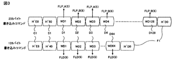
≪フラッシュメモリへの書き込みの動作≫
図3は、本発明の1つの実施形態によるフラッシュメモリへの書き込みの動作を示す図である。
<< Operation to write to flash memory >>
FIG. 3 is a diagram illustrating a write operation to a flash memory according to one embodiment of the present invention.
メインCPU2によるストア命令発行などによって、フラッシュメモリ書き込み用コマンド発行用に割り当てられたアドレスに対して周辺バスPBUSライトを発行すると、FCU8は周辺バスPBUSライトの内容に対応した処理を実行する。
When a peripheral bus PBUS write is issued to an address assigned for issuing a flash memory write command by issuing a store instruction by the main CPU 2, the
最初の周辺バスPBUSのライトアクセス(C1)のデータはコマンドの種類を決定するためのサイクルであり、メインCPU2がFCU8に対してフラッシュメモリの書き込みを要求する場合にはH´E8をライトする周辺バスPBUSアクセスを発行すればよい。
The first write access (C1) data of the peripheral bus PBUS is a cycle for determining the type of command. When the main CPU 2 requests the
次の周辺バスPBUSのライトアクセス(S1)は、メインCPU2が書き込みデータのサイズを16ビット単位で決定するためのサイクルである。FLP_A(5)とFLP_B(6)とに対して合計256バイトの書き込みの場合にはH´80をライトする周辺バスPBUSアクセスをメインCPU2が発行して、FLD9に対して合計128バイトの書き込みの場合にはH´40をライトする周辺バスPBUSアクセスをメインCPU2が発行すればよい。 The next write access (S1) of the peripheral bus PBUS is a cycle for the main CPU 2 to determine the size of write data in units of 16 bits. In the case of writing 256 bytes in total for FLP_A (5) and FLP_B (6), the main CPU 2 issues a peripheral bus PBUS access for writing H'80 and writes 128 bytes in total for FLD9. In this case, the main CPU 2 may issue a peripheral bus PBUS access for writing H'40.
アクセスS1よりも後の周辺バスPBUSのライトアクセス(D1〜D128)は、16ビット単位(2バイト単位)で書き込みデータを転送するためのサイクルである。 The write access (D1 to D128) of the peripheral bus PBUS after the access S1 is a cycle for transferring write data in units of 16 bits (2 bytes).
図3の上に示すようにFLP_A(5)とFLP_B(6)とに対して合計256バイト書き込みの場合には、128回(D1〜D128)の周辺バスPBUSのライトアクセスを発行する。FCU8は1回目(D1)から128回目(D128)までのデータをFLP_A(5)およびFLP_B(6)のデータラッチへインターリーブで連続してシリアルデータ転送する。FLP_A(5)とFLP_B(6)はインターリーブで交互にアクセスされるため、奇数回目(D1、D3、・・・・、D127)のデータはFLP_A(5)のデータラッチに格納され、偶数回目(D2、D4、・・・・、D128)のデータはFLP_B(6)のデータラッチに格納されることになる。
As shown in the upper part of FIG. 3, in the case of writing a total of 256 bytes to FLP_A (5) and FLP_B (6), 128 times (D1 to D128) write access of the peripheral bus PBUS is issued. The
図3の下に示すようにFLD9に対して合計128バイト書き込みの場合には、64回(D1〜D64)の周辺バスPBUSのライトアクセスを発行すればFLD9のデータラッチへ連続してシリアルデータ転送が実行される。
As shown in the lower part of FIG. 3, in the case of writing 128 bytes to the
また、書き込み先のフラッシュメモリのアドレスはD1サイクルにおける周辺バスPBUSアクセスのアドレスによって決定される。書き込みデータの転送が完了した後に、H´D0をライトする周辺バスPBUSのアクセス(F1)を発行する。すると、図3の上の256バイトの書き込みの場合には、FCU8はFLP_A(5)とFLP_B(6)とに関してラッチへ転送されたWD1〜W128のデータをフラッシュメモリアレーへ並列内部書き込み処理を行う。図3の下の128バイトの書き込みの場合には、FCU8は
FLD9に対して、WD1〜W64のデータをラッチからフラッシュメモリアレーへ連続的に書き込む内部書き込み処理を実行する。
Further, the address of the flash memory to be written is determined by the address of the peripheral bus PBUS access in the D1 cycle. After the transfer of the write data is completed, the access (F1) of the peripheral bus PBUS for writing H′D0 is issued. Then, in the case of 256-byte writing in the upper part of FIG. 3, the
フラッシュメモリの書き込みデータに先行する書き込みコマンドに、書き込みサイズを指定するS1サイクルが存在している。従って、FCU8はS1サイクルで指定されたサイズの書き込みデータの転送完了を待つだけでよく、FCU8の制御を簡素化できる。書き込みデータの転送が完了すると、FCU8はフラッシュメモリのラッチに転送されたデータをフラッシュメモリアレーへプログラムとベリファイとの反復による内部書き込み処理を実行する。もし、S1サイクルが存在しない場合には、FCU8が書き込み先のフラッシュメモリの種類を判定して書き込みデータのサイズを決定する必要があり、制御が複雑になる。
In the write command preceding the write data in the flash memory, there is an S1 cycle for specifying the write size. Therefore, the
また、書き込みサイズが全く異なるフラッシュメモリへ書き込みを行う場合にも、S1サイクルで指定されたサイズの書き込みデータの転送完了を待つ制御を変更する必要がない。このため、フラッシュメモリの追加・変更が発生しても、FCU8を変更せずに対応することが可能である。
Even when writing to flash memories having completely different write sizes, there is no need to change the control for waiting for completion of transfer of write data of the size specified in the S1 cycle. For this reason, even if addition or change of the flash memory occurs, it is possible to cope without changing the
書き込みサイズを指定するサイクル(S1)に要する時間は、データ転送用のサイクル(D1〜D128)やFCU8によるフラッシュメモリ書き込み処理に要する時間と比較して短い。従って、S1サイクルのフラッシュメモリへの書き込み動作に要する時間に対する悪影響は、ほとんどない。
The time required for the cycle (S1) for designating the write size is shorter than the time required for the data transfer cycle (D1 to D128) and the flash memory write processing by the
図4は、本発明の他の実施形態によるフラッシュメモリへの書き込みの動作を示す図である。この動作は、16ビット単位(2バイト単位)毎のデータ転送が行われるフラッシュメモリがFLP_A(5)とFLP_B(6)との間で交代する256バイトのインターリーブの書き込みである。インターリーブの書き込みを行うためのコマンドが図3の上の256バイト書き込みコマンドと相違するのは、最初のサイクル(C2)における書き込みデータの値がH´E9であることである。 FIG. 4 is a diagram illustrating a write operation to a flash memory according to another embodiment of the present invention. This operation is a 256-byte interleaved writing in which the flash memory to which data transfer is performed every 16 bits (2 bytes) is alternated between FLP_A (5) and FLP_B (6). The command for performing the interleaved write is different from the 256-byte write command in FIG. 3 in that the value of the write data in the first cycle (C2) is H′E9.
256バイトのインターリーブ書き込みコマンドの最終サイクル(F1)に対応する周辺バスPBUSのライトアクセスが発行されると、FCU8はFLP_A(5)とFLP_B(6)に対する内部書き込み処理を開始する。インターリーブの書き込みコマンドに対する書き込み処理では、FCU8は最初に奇数番のデータWD1、WD3…WD127の128バイトのデータをFLP_A(5)のラッチからFLP_A(5)フラッシュメモリアレーへ転送して内部書き込みを実行する。その後、FCU8は偶数番のデータWD2、WD4…WD128の128バイトのデータをFLP_B(6)のラッチからFLP_B(6)のフラッシュメモリアレーへ転送して内部書き込みを実行する。
When a write access to the peripheral bus PBUS corresponding to the final cycle (F1) of the 256-byte interleaved write command is issued, the
図4に示した256バイトのインターリーブ書き込みコマンドで要求された書き込みをFCU8が実行する際には、書き込みデータをFLP_A(5)用とFLP_B(6)用とに分類して転送データを事前に準備する。その後、コマンド発行時の周辺バスPBUSのライトアクセスで書き込まれたのとは異なる順番の事前準備データを転送する必要がある。
When the
一方、図3の上に示した256バイトの書き込みコマンドでは、コマンド発行時の周辺バスPBUSのライトアクセスと同じ順番でデータをFLP_A(5)、FLP_B(6)へFCU8が転送する。図4に示した256バイトのインターリーブコマンドでは、最初のサイクル(C2)でインターリーブ書き込みであることが指定されている。従って、FCU8が書き込み先のフラッシュメモリの種類を判定して書き込みデータの書き込み順を切り替える制御をする必要がなく、事前準備データを転送すればよいので、FCU8の制御を簡素化できる。
On the other hand, in the 256-byte write command shown in FIG. 3, the
フラッシュメモリに書き込み単位分のデータを書き込む期間は、書き込み先のメモリに高電圧を印加する必要がある。256バイトのデータをFLP_A(5)とFLP_B(6)とに並列内部書き込みを行う図3の上の方式の場合、FLP_A(5)とFLP_B(6)とに同時に高電圧を印加する必要があるため、電源供給能力を大きくしなければならない。図4の方式では、最初にFLP_A(5)に128バイト分のデータを内部書き込みした後に、FLP_B(6)に128バイト分のデータを内部書き込みするため、FLP_A(5)とFLP_B(6)とに同時に高電圧を印加する必要がなく、電源供給能力を大きくする必要がない。 A high voltage needs to be applied to the write destination memory during a period of writing data for the write unit in the flash memory. In the case of the upper method in FIG. 3 in which 256-byte data is written in parallel to FLP_A (5) and FLP_B (6), it is necessary to apply a high voltage to FLP_A (5) and FLP_B (6) simultaneously. Therefore, the power supply capacity must be increased. In the method of FIG. 4, since 128 bytes of data are first internally written to FLP_A (5) and then 128 bytes of data are internally written to FLP_B (6), FLP_A (5) and FLP_B (6) It is not necessary to apply a high voltage simultaneously, and it is not necessary to increase the power supply capability.
≪フラッシュ制御ユニットの構成≫
図5は、図1のシングルチップマイクロプロセッサ1の内部のフラッシュ制御ユニット(FCU)5の内部構成を示す図である。
≪Configuration of flash control unit≫
FIG. 5 is a diagram showing an internal configuration of a flash control unit (FCU) 5 inside the
同図に示すようにFCU8は、サブCPU(FCPU)12以外にも、フラッシュCPUインタフェースコントローラ(FIMC)13、フラッシュバス制御回路(FBSC)14、コントロールRAM(CRAM)15、フラッシュ書き込み・消去制御回路(FLC)16、誤り訂正回路(ECC)33、フラッシュバスFBUSを有する。FCU8はメインCPU2のアドレス空間に配置され、メインCPU2は周辺バスPBUSを経由してFCU8の内部をアクセスすることができる。すなわち、フラッシュCPUインタフェースコントローラ13(FIMC)は周辺バスPBUSに接続され、メインCPU2からのアクセスに対してFCU8の全体的な制御を行う。FIMC13はFCPU12に割り込み要求信号IRQと対応するベクタとを発行して、FCPU12を起動する。また、FIMC13はフラッシュバス制御回路(FBSC)14にバスコマンドを発行することによって、コントロールRAM15及びFLC16に対するフラッシュバスFBUS経由のバス制御を行う。コントロールRAM15はFCPU12のフラッシュ書き込み・消去の動作プログラムの格納領域、或いはFCPU12のワーク領域等に用いられる。FLC16は、フラッシュメモリ5、6、9に対する動作制御レジスタ(FCNTR)18、消去ブロック指定レジスタ(EBLKR)17及びトリミングレジスタを有する。FLC16は、動作制御レジスタ18に設定される制御ビットの状態に従って、フラッシュメモリ5、6、9の書き込み・消去の動作を制御する。動作制御レジスタ18の制御ビットは、例えば書き込みイネーブルビットWE、書き込み指示ビットP、及び消去指示ビットE等とされている。書き込みイネーブルビットWEは、論理値“1”によって書き込み・消去動作の指示の有効性を示す。書き込み指示ビットPは、論理値“1”によって書き込みパルス電圧の印加を指示する。消去指示ビットEは、論理値“1”によって消去パルス電圧の印加を指示する。FLC16のトリミングレジスタには、フラッシュメモリ5、6、9の書き込みパルス電圧、消去パルス電圧、ドレイン電圧、ソース電圧、ベリファイ電圧の各々の電圧レベルの微調整や、書き込みパルス電圧及び消去パルス電圧のパルス幅の微調整を行うためのトリミングデータが設定される。
As shown in the figure, in addition to the sub CPU (FCPU) 12, the
トリミングデータやFCPU12の書き込み・消去の動作プログラムの初期値はフラッシュメモリ9が保有しており、トリミングデータと書き込み・消去の動作プログラムとはパワーオンリセットに応答してメインCPU2、データ転送コントローラ(DTC、図示せず)、ダイレクトメモリアクセスコントローラ(DMAC、図示せず)のいずれかがトリミングデータレジスタ及びコントロールRAM15とにそれぞれ内部転送することが可能である。トリミングデータレジスタ及びコントロールRAM15のプログラム領域は通常モードではユーザープログラムを実行しているメインCPU2からの書き込みアクセス不可能にされ、保護されている。しかし、テストモードでは、これらはメインCPU2により自由にアクセス可能にされる。消去ブロック指定レジスタ17には、消去ブロック又は消去アドレスが設定される。書き込みデータ及び書き込みアドレスは、フラッシュメモリ内部のデータレジスタ及びアドレスレジスタにセットされる。
The initial values of the trimming data and the write / erase operation program of the
割り込みによるFCPU12の起動について、説明する。FIMC13は、メインCPU2から周辺バスPBUSを経由してアクセス可能にされる内部I/Oレジスタ(IIOR)20、コントロールレジスタ(CNTR)21、ステータスレジスタ(STSR)22、割り込み制御レジスタ(INTR)31、CRAM制御レジスタ(CRCNTR)32を有する。コントロールレジスタ21は書き込み・消去フラグFENTRY等の設定領域とされ、メインCPU2によって書き込み可能にされ、FCPU12によって読み出し可能にされている。ステータスレジスタ22はビジーフラグBUSYやコマンドエンドフラグCMDE等の記憶領域とされ、FCPU12によって書き込み可能にされ、メインCPU2によって読み出し可能にされている。また、FCPU12は経路23からステータスレジスタ22に対する書き込みを行う。割り込み制御レジスタ31の割り込みイネーブルビットINTENがセットされている状態でステータスレジスタ22のエラービットERRが誤り訂正回路33によりセットされると、誤り割り込み信号ERRINTがアサートされて、バスコントローラ4を経由してメインCPU2に割り込み要求が通知される。誤り訂正回路33はコントロールRAM15に格納されたFCU12の書き込み・消去制御プログラムのソフトエラーによるデータ誤りを検出すると、ステータスレジスタ22にエラービットERRをセットして、フラッシュメモリ5、6からCRAM15へのFCU12の書き込み・消去制御プログラムの再転送を要求する。再転送されたFCU12の書き込み・消去制御プログラムをCRAM15へ書き込むために、CRAM制御レジスタ32のCRAMアクセスイネーブルビットCRENがセットされる。CRAMアクセスイネーブルビットCRENはCRAMアクセス通知信号CRAMENに反映されて、CRAMアクセス通知信号CRAMENはバスコントローラ4へ供給される。バスコントローラ4は内部バスIBUS上のフラッシュメモリ5、6から読み出されたFCU12の書き込み・消去制御プログラムを周辺バスPBUSに転送するので、メインCPU2、DTC、DMACのいずれかがBSC4を経由してCRAM15へのFCU12の書き込み・消去制御プログラムの再転送を実行する。
The activation of the
通常モードにおいて書き込み・消去フラグFENTRY=“1”の時に、メインCPU2からフラッシュメモリ5、6、9の不揮発性メモリアレイにマッピングされたアドレスにデータを書き込むアクセスをFIMC13が検出すると、その書き込みアクセスをFIMC13はフラッシュ書き込みコマンドとして認識する。また、メインCPU2から消去ブロック指定レジスタ17に消去アドレス若しくは消去ブロック指定情報を書込むアクセスをFIMC13が検出すると、その書き込みアクセスをFIMC13はフラッシュ消去コマンドとして認識する。FIMC13はそのコマンド解釈に従ってFCPU12への割り込み要求信号IRQを活性化して、コマンドに応ずるベクタを発行する。これによってFCPU12は、ベクタによって指定される書き込み制御プログラム又は消去制御プログラムをコントロールRAM15からフェッチして実行する。フラッシュ書き込みコマンドに応答する場合、FCPU12はその書き込み制御プログラムに従ってフラッシュ書き込みコマンドと認識した書き込みアクセスに係るアドレスとデータを内部IOレジスタ20からコントロールRAM15に取り込み、フラッシュメモリに転送して、FLC16内部のFCNTR18のWE、Pビット等を順次設定しながら、フラッシュメモリ5、6、9に対する書き込みを行う。フラッシュ消去コマンドに応答する場合、FCPU12はその消去制御プログラムに従ってフラッシュ消去コマンドと認識した消去ブロック指定データを内部IOレジスタ20からコントロールRAM15に取り込み、フラッシュメモリに転送して、FLC16内部のFCNTR18のWE、Eビット等を順次設定しながら、フラッシュメモリ5、6、9に対する消去を行う。
When the write / erase flag FENTRY = “1” in the normal mode, when the
FCU8からの書き込み・消去フラグFENTRYは、FIMC13からバスコントローラ(BSC)6に供給される。通常モードにおいて書き込み・消去フラグFENTRY=“0”の時に、フラッシュメモリ5、6、9のマッピングアドレス又は消去ブロック指定レジスタ17に対するメインCPU2からの書き込みアクセスをBSC4が検出すると、例えばアドレスエラーを発生させてフラッシュメモリ5、6、9への書き込み動作を無効とする。従って、通常モードにおいて書き込み・消去フラグFENTRY=“0”の時には、フラッシュメモリ5、6、9には内部バスIBUS経由のリードアクセスだけが可能にされる。尚、テストモードでは書き込み・消去フラグFENTRYはBSC4によるフラッシュメモリ5、6、9に対するアクセス経路の制御だけに用いられる。すなわち、フラッシュメモリ5、6、9に対しては、テストモードにおいてFENTRY=1の時にはBSC4及び周辺バスPBUS経由のアクセスだけが許容され、FENTRY=“0”の時には内部バスIBUS経由のリードアクセスだけが許容される。
The write / erase flag FENTRY from the
フラッシュバス制御回路(FBSC)14を経由するコントロールRAM15及びFLC16のアクセス制御について、説明する。通常モード及びテストモードのいずれにおいても、フラッシュ制御ユニット(FCU)5のマッピングアドレス(消去ブロック指定レジスタ17のマッピングアドレスを除く)に対するメインCPU2またはDTC、DMACのいずれかからのアクセスに対して、CPUインタフェースコントローラ(FIMC)13はアクセスコマンドをFBSC14に発行する。発行されたアクセスコマンドに従ってFBSC14は、フラッシュバスFBUSの制御を行ってコントロールRAM15及びFLC16へのリードアクセス及びライトアクセスを行うことができる。特に制限されないが、通常モードではFLC16のトリミングレジスタに対する自由なアクセスは許容されていない。しかし、テストモードでは、メインCPU2からフラッシュメモリ5、6、9のマッピングアドレスにデータを書き込むアクセスがあっても、また、メインCPU2から消去ブロック指定レジスタ17に対してデータを書き込むアクセスがあっても、CPUインタフェースコントローラ13はFCPU12を起動せず、対応するアクセスコマンドをFBSC14に発行する。それに従ってFBSC14がフラッシュバスFBUSの制御を行って、CPUインタフェースコントローラ13の内部IOレジスタ20に保持された書き込みデータ及び書き込みアドレスをフラッシュメモリ5、6、9に供給して、又は消去ブロックアドレスを消去ブロック指定レジスタ17に供給する。この後、メインCPU2はFLC16のレジタ18に対する書き込みアクセスを発行することによって消去ビットEやプログラムビットPを直接操作して、消去動作又は書き込み動作を行うことができる。
The access control of the
テストモードでは、メインCPU2はFLC16のトリミングレジスタを直接操作することができるから、トリミングデータの設定次第で、例えば、フラッシュメモリ5、6、9における書き込みパルス電圧、消去パルス電圧、パルス印加時間、ドレイン電圧、及びソース電圧等を微調整することができる。そのような電圧や時間を微調整することによって、マイクロコンピュータ1の製造プロセス、不揮発性メモリの素子構成、あるいはマイクロコンピュータ1の個体差などに即して、最適な書き込み、最適な消去の制御が可能にされる。これらの電圧や時間は量産時には固定にされるのがよいが、少なくとも試作評価時には可変にする必要がある。
In the test mode, since the main CPU 2 can directly operate the trimming register of the
更にテストモードでは、メインCPU2はコントロールRAM15に格納されたFCPU12の書き込み・消去制御プログラムを書き換えることができる。試作評価時には、テストモードで、メインCPU2による制御プログラム実行で書き込み・消去を実行して、基本機能や必要なパラメータなどの確認を行うことができる。試作評価時は、機器制御を行うわけではないので、リアルタイム性の要求される割り込み処理などを考慮する必要がない。
Further, in the test mode, the main CPU 2 can rewrite the program / erase control program of the
図5に示したFCU8のエラー訂正回路(ECC)33は、コントロールRAM(CRAM)15の格納データが破壊されたことを検出するための回路である。フラッシュバスFBUSを経由してCRAM15に対する書き込みが実行される場合には、ECC33がFBUSから出力されたデータに対応したエラー訂正符号を生成して、書き込みデータとともにエラー訂正符号をCRAM15に書き込む。フラッシュバスFBUSを経由してCRAM15に対する読み出しが実行される場合には、ECC33がCRAM15から読み出されたデータとエラー訂正符号に基づいて読み出しデータを生成して、フラッシュバスFBUSに出力する。読み出しデータ生成時に、ECC33がCRAM15から読み出されたデータまたはエラー訂正符号に誤りを検出すると、ECCエラー信号ECCERRがアサートされる。FIMC13のステータスレジスタ(STSR)22のエラービットERRは、ECCエラー信号ECCERRがアサートされるとセットされるフラグである。割り込み制御レジスタ(INTR)31の割り込みイネーブルビットINTENがセットされた状態で、STSR22のエラービットERRがセットされると、エラー割り込み信号ERRINTがアサートされて、メインCPU2に割り込み要求が通知される。すると、メインCPU2、DTC、DMACのいずれかを用いて、フラッシュメモリ5、6に格納されたFCU8のFCPU12によるフラッシュメモリ5、6、9の書き込み・消去制御プログラムのデータをFCU8のCRAM15へ再転送するものである。
The error correction circuit (ECC) 33 of the
尚、CRAM制御レジスタ(CRCNTR)32のCRAMアクセスイネーブルビットCRENは、CRAM15へのアクセス許可・禁止を制御するためのビットである。CRAMアクセスイネーブルビットCRENが“0”の場合にはCRAM15へのアクセスは禁止され、“1”の場合にはCRAM15へのアクセスが許可される。CRAMアクセス通知信号CRAMENはCRAMアクセスイネーブルビットCRENの値をFCU8からBSC4に通知するための信号である。BSC4は、CRAMアクセス通知信号CRAMENがアサートされている場合のみ、CRAM15に対する内部バスIBUSのアクセスを周辺バスPBUSに伝播する。しかし、CRAMアクセス通知信号CRAMENがネゲートされた状態で発行されたCRAM15に対するアクセスは、無効化される。
The CRAM access enable bit CREN of the CRAM control register (CRCNTR) 32 is a bit for controlling permission / prohibition of access to the
このマイクロコンピュータ1では、システム起動後にフラッシュメモリ4に格納されたユーザープログラムのメインCPU2による実行と並行して、DTC、DMACのいずれかを使用してフラッシュメモリ5、6からCRAM15にFCU8のFCPU12によるフラッシュメモリ5、6、9の書き込み・消去制御プログラムを転送することが可能である。また、システムの起動後にメインCPU2がFCPU12によるフラッシュメモリ5、6、9の書き込み・消去制御プログラムをフラッシュメモリ5、6からCRAM15に転送することも可能である。
In this
更に、このマイクロコンピュータ1では、メインCPU2によりFCU8のFIMC13のSTSR22のエラービットERRを読み出し、またはエラー割り込み信号ERRINTによって、CRAM15の格納データが破壊されているかどうかを判定することが可能である。CRAM15の格納データが破壊された場合には、FCU8のFCPU12によるフラッシュメモリ5、6、9の書き込み・消去制御プログラムのプログラムをメインCPU2、DTC、DMACのいずれかがフラッシュメモリ5、6からCRAM15へ再転送するため、FCU8の誤動作を防止して、マイクロコンピュータの信頼性を向上することができると言う効果が得られる。
Further, in the
以上本発明者によってなされた発明を実施形態に基づいて具体的に説明したが、本発明はそれに限定されるものではなく、その要旨を逸脱しない範囲において種々変更可能であることは言うまでもない。 Although the invention made by the present inventor has been specifically described based on the embodiments, it is needless to say that the present invention is not limited thereto and can be variously modified without departing from the gist thereof.
以上の説明では主として本発明者によってなされた発明をその背景となった利用分野であるシングルチップマイクロコンピュータに適用した場合について説明したが、それに限定されるものではなく、その他の半導体集積回路装置、例えば、マイクロコントローラ、デジタルシグナルプロセッサ(DSP)を中心にした半導体集積回路装置にも適用可能である。 In the above description, the case where the invention made mainly by the present inventor is applied to a single chip microcomputer which is a field of use as the background has been described. However, the present invention is not limited thereto, and other semiconductor integrated circuit devices, For example, the present invention can be applied to a semiconductor integrated circuit device centered on a microcontroller and a digital signal processor (DSP).
さらに不揮発性メモリとしては、フラッシュメモリ等のように電荷蓄積領域に電荷を注入したり電荷蓄積領域から電荷を放出するタイプ以外に、例えば相変化メモリも採用することができる。例えば、相変化メモリの消去はメモリセルの抵抗に電流を流すことにより抵抗を溶融した後に電流を激減させることで多結晶化して高抵抗とし、相変化メモリの書き込みはメモリセルの抵抗に電流を流すことにより抵抗を溶融した後に電流を徐々に減少させることで単結晶化して低抵抗とすることで実現することができる。この相変化メモリでも、消去処理や書き込み処理は消去または書き込みの電流パルスの印加とベリファイ動作との反復処理となる。本発明は少なくとも、不揮発性メモリとデータ処理装置を内蔵した半導体集積回路装置に適用することができる。 Further, as a nonvolatile memory, for example, a phase change memory can be employed in addition to a type in which charges are injected into or discharged from a charge storage region such as a flash memory. For example, erasing a phase change memory causes a current to flow through the resistance of the memory cell, melts the resistance, and then sharply reduces the current to make it polycrystallized to have a high resistance. This can be realized by reducing the current by gradually reducing the current after melting the resistance by flowing it into a single crystal. Even in this phase change memory, the erase process and the write process are repeated processes of applying an erase or write current pulse and a verify operation. The present invention can be applied to at least a semiconductor integrated circuit device incorporating a nonvolatile memory and a data processing device.
1 シングルチップマイクロコンピュータ
2 中央処理ユニット(CPU)
3 ランダムアクセスメモリ(RAM)
4 バスコントローラ(BSC)
FLM フラッシュモジュール
5 プログラム格納フラッシュ
6 プログラム格納フラッシュ
7 プログラム格納フラッシュ読み出しバッファ
8 フラッシュ制御ユニット
9 データ格納フラッシュ
10 システムコントローラ(SYSC)
MD0〜MD2 モード端子
11 周辺回路(PRHRL)
12 I/Oポート(IOP)
内部バスIBUS 内部バス
周辺バスPBUS 周辺バス
EXBUS 外部バス
1 Single-chip microcomputer 2 Central processing unit (CPU)
3 Random access memory (RAM)
4 Bus controller (BSC)
MD0 to MD2 Mode terminal 11 Peripheral circuit (PRHRL)
12 I / O port (IOP)
Internal bus IBUS Internal bus Peripheral bus PBUS Peripheral bus EXBUS External bus
Claims (18)
前記不揮発性メモリモジュールは、不揮発性メモリと、不揮発制御ユニットとを含み、
前記メインCPUから発行されたコマンドに応答して前記不揮発制御ユニットは前記不揮発性メモリの書き込み及び消去の制御を行うものであり、
前記不揮発性メモリは、前記メインCPUが実行するプログラムを格納するプログラム格納不揮発性メモリと、前記メインCPUによる前記プログラムの命令実行結果のデータを格納するデータ格納不揮発性メモリとを含み、
前記不揮発制御ユニットによる前記プログラム格納不揮発性メモリへのプログラム書き込みのデータサイズは、前記不揮発制御ユニットによる前記データ格納不揮発性メモリへのデータ書き込みのデータサイズと異なるサイズに設定され、
前記メインCPUは前記不揮発制御ユニットに前記プログラム格納不揮発性メモリへのプログラム書き込みの要求を行う際に前記プログラム書き込みのデータサイズに対応する第1のサイズ情報を前記不揮発制御ユニットへ供給して、
前記メインCPUは前記不揮発制御ユニットに前記データ格納不揮発性メモリへのデータ書き込みの要求を行う際に前記データ書き込みのデータサイズに対応する第2のサイズ情報を前記不揮発制御ユニットへ供給して、
前記不揮発制御ユニットは前記メインCPUから供給される前記第1のサイズ情報に応答して前記不揮発性メモリの前記プログラム格納不揮発性メモリにプログラムの書き込みを実行するものでありまた前記メインCPUから供給される前記第2のサイズ情報に応答して前記不揮発性メモリの前記データ格納不揮発性メモリにデータの書き込みを実行するものである半導体集積回路。 Comprising a main CPU and an electrically writable and erasable nonvolatile memory module;
The nonvolatile memory module includes a nonvolatile memory and a nonvolatile control unit,
In response to a command issued from the main CPU, the nonvolatile control unit controls writing and erasing of the nonvolatile memory,
The nonvolatile memory includes a program storing nonvolatile memory for storing a program executed by the main CPU, and a data storing nonvolatile memory for storing data of an instruction execution result of the program by the main CPU,
The data size of the program write to the program storage nonvolatile memory by the nonvolatile control unit is set to a size different from the data size of the data write to the data storage nonvolatile memory by the nonvolatile control unit,
The main CPU supplies first size information corresponding to the data size of the program writing to the nonvolatile control unit when making a request for writing the program to the program storing nonvolatile memory to the nonvolatile control unit,
When the main CPU requests the nonvolatile control unit to write data to the data storage nonvolatile memory, the main CPU supplies second size information corresponding to the data size of the data write to the nonvolatile control unit,
The nonvolatile control unit executes a program write to the program storing nonvolatile memory of the nonvolatile memory in response to the first size information supplied from the main CPU, and is supplied from the main CPU. A semiconductor integrated circuit that executes data writing to the data storage nonvolatile memory of the nonvolatile memory in response to the second size information .
前記プログラム格納不揮発性メモリには、前記不揮発制御ユニットの前記サブCPUによる前記不揮発性メモリの書き込みおよび消去を制御する書き込み・消去制御プログラムが格納され、
システム起動時には前記プログラム格納不揮発性メモリに格納された前記書き込み・消去制御プログラムが前記不揮発制御ユニットの前記コントロールメモリへ転送され、
前記不揮発性メモリの書き込み及び消去の制御は前記メインCPUから発行されたコマンドに応答して前記不揮発制御ユニットの前記サブCPUが前記コントロールメモリに転送された書き込み・消去制御プログラムの命令を実行することにより行われるものである請求項1から請求項5のいずれかに記載の半導体集積回路。 The nonvolatile control unit includes a sub CPU and a control memory,
The program storing nonvolatile memory stores a writing / erasing control program for controlling writing and erasing of the nonvolatile memory by the sub CPU of the nonvolatile control unit,
At the time of system startup, the program / erase control program stored in the program storage nonvolatile memory is transferred to the control memory of the nonvolatile control unit,
Control of writing and erasing of the non-volatile memory is performed in response to a command issued from the main CPU, and the sub CPU of the non-volatile control unit executes a command of the writing / erasing control program transferred to the control memory. The semiconductor integrated circuit according to claim 1, wherein the semiconductor integrated circuit is performed by:
前記不揮発性メモリモジュールは、不揮発性メモリと、不揮発制御ユニットとを含み、
前記メインCPUから発行されたコマンドに応答して前記不揮発制御ユニットは前記不揮発性メモリの書き込み及び消去の制御を行うものであり、
前記不揮発性メモリは、前記メインCPUが実行するプログラムを格納するプログラム格納不揮発性メモリと、前記メインCPUによる前記プログラムの命令実行結果のデータを格納するデータ格納不揮発性メモリとを含み、
前記不揮発制御ユニットによる前記プログラム格納不揮発性メモリへのプログラム書き込みのデータサイズは、前記不揮発制御ユニットによる前記データ格納不揮発性メモリへのデータ書き込みのデータサイズと異なるサイズに設定され、
前記メインCPUは前記不揮発制御ユニットに前記プログラム格納不揮発性メモリへのプログラム書き込みの要求を行う際にプログラム書き込みのデータサイズに対応する第1のサイズ情報を前記不揮発制御ユニットへ供給して、
前記メインCPUは前記不揮発制御ユニットに前記データ格納不揮発性メモリへのデータ書き込みの要求を行う際にデータ書き込みのデータサイズに対応する第2のサイズ情報を前記不揮発制御ユニットへ供給して、
前記不揮発制御ユニットは前記メインCPUから供給される前記第1のサイズ情報に応答して前記不揮発性メモリの前記プログラム格納不揮発性メモリにプログラムの書き込みを実行するものでありまた前記メインCPUから供給される前記第2のサイズ情報に応答して前記不揮発性メモリの前記データ格納不揮発性メモリにデータの書き込みを実行するものであるシングルチップマイクロコンピュータ。 Comprising a main CPU and an electrically writable and erasable nonvolatile memory module;
The nonvolatile memory module includes a nonvolatile memory and a nonvolatile control unit,
In response to a command issued from the main CPU, the nonvolatile control unit controls writing and erasing of the nonvolatile memory,
The nonvolatile memory includes a program storing nonvolatile memory for storing a program executed by the main CPU, and a data storing nonvolatile memory for storing data of an instruction execution result of the program by the main CPU,
The data size of the program write to the program storage nonvolatile memory by the nonvolatile control unit is set to a size different from the data size of the data write to the data storage nonvolatile memory by the nonvolatile control unit,
The main CPU supplies the nonvolatile control unit with the first size information corresponding to the data size of the program write when requesting the nonvolatile control unit to write the program to the program storage nonvolatile memory.
When the main CPU requests the nonvolatile control unit to write data to the data storage nonvolatile memory, the main CPU supplies second size information corresponding to the data size of data writing to the nonvolatile control unit,
The nonvolatile control unit executes a program write to the program storing nonvolatile memory of the nonvolatile memory in response to the first size information supplied from the main CPU, and is supplied from the main CPU. A single-chip microcomputer for executing data writing in the data storage nonvolatile memory of the nonvolatile memory in response to the second size information .
前記プログラム格納不揮発性メモリには、前記不揮発制御ユニットの前記サブCPUによる前記不揮発性メモリの書き込みおよび消去を制御する書き込み・消去制御プログラムが格納され、
システム起動時には前記プログラム格納不揮発性メモリに格納された前記書き込み・消去制御プログラムが前記不揮発制御ユニットの前記コントロールメモリへ転送され、
前記不揮発性メモリの書き込み及び消去の制御は前記メインCPUから発行されたコマンドに応答して前記不揮発制御ユニットの前記サブCPUが前記コントロールメモリに転送された書き込み・消去制御プログラムの命令を実行することにより行われるものである請求項7から請求項11のいずれかに記載のシングルチップマイクロコンピュータ。 The nonvolatile control unit includes a sub CPU and a control memory,
The program storing nonvolatile memory stores a writing / erasing control program for controlling writing and erasing of the nonvolatile memory by the sub CPU of the nonvolatile control unit,
At the time of system startup, the program / erase control program stored in the program storage nonvolatile memory is transferred to the control memory of the nonvolatile control unit,
Control of writing and erasing of the non-volatile memory is performed in response to a command issued from the main CPU, and the sub CPU of the non-volatile control unit executes a command of the writing / erasing control program transferred to the control memory. The single-chip microcomputer according to any one of claims 7 to 11, wherein the single-chip microcomputer is performed by the following.
前記データまたはプログラム書き込みのデータサイズに対応したサイズ情報と、
書き込まれるべきデータ情報と、を含むとされる請求項2記載の半導体集積回路。 The write command for the nonvolatile memory from the main CPU is:
Size information corresponding to the data size of the data or program write,
3. The semiconductor integrated circuit according to claim 2, further comprising data information to be written.
前記データまたはプログラム書き込みのデータサイズに対応したサイズ情報と、
書き込まれるべきデータ情報と、を含むとされる請求項8記載のシングルチップマイクロコンピュータ。 The write command for the nonvolatile memory from the main CPU is:
Size information corresponding to the data size of the data or program write,
9. The single chip microcomputer according to claim 8, wherein the single chip microcomputer includes data information to be written.
前記不揮発制御ユニットが接続される第2バスと、を有し、
前記プログラム格納不揮発性メモリは、前記第1バスを介して前記メインCPUからの読み出し動作を行い、
前記データ格納不揮発性メモリは、前記第2バスを介して前記メインCPUからの読み出し動作を行うとされる請求項1または13記載の半導体集積回路。 A first bus to which the main CPU is connected;
A second bus to which the nonvolatile control unit is connected,
The program storing nonvolatile memory performs a read operation from the main CPU via the first bus,
The semiconductor integrated circuit according to claim 1, wherein the data storage nonvolatile memory performs a read operation from the main CPU via the second bus.
前記不揮発制御ユニットが接続される第2バスと、を有し、
前記プログラム格納不揮発性メモリは、前記第1バスを介して前記メインCPUからの読み出し動作を行い、
前記データ格納不揮発性メモリは、前記第2バスを介して前記メインCPUからの読み出し動作を行うとされる請求項7または14記載のシングルチップマイクロコンピュータ。 A first bus to which the main CPU is connected;
A second bus to which the nonvolatile control unit is connected,
The program storing nonvolatile memory performs a read operation from the main CPU via the first bus,
The single-chip microcomputer according to claim 7 or 14, wherein the data storage nonvolatile memory performs a read operation from the main CPU via the second bus.
前記メインCPUからの前記書き込みコマンドを前記第2バス経由で供給されてなる請求項15記載の半導体集積回路。 The nonvolatile control unit is connected to the second bus,
16. The semiconductor integrated circuit according to claim 15, wherein the write command from the main CPU is supplied via the second bus.
前記メインCPUからの前記書き込みコマンドを前記第2バス経由で供給されてなる請
求項16記載のシングルチップマイクロコンピュータ。 The nonvolatile control unit is connected to the second bus,
17. The single-chip microcomputer according to claim 16, wherein the write command from the main CPU is supplied via the second bus.
Priority Applications (1)
| Application Number | Priority Date | Filing Date | Title |
|---|---|---|---|
| JP2006232273A JP5013450B2 (en) | 2006-08-29 | 2006-08-29 | Semiconductor integrated circuit and single chip microcomputer |
Applications Claiming Priority (1)
| Application Number | Priority Date | Filing Date | Title |
|---|---|---|---|
| JP2006232273A JP5013450B2 (en) | 2006-08-29 | 2006-08-29 | Semiconductor integrated circuit and single chip microcomputer |
Publications (3)
| Publication Number | Publication Date |
|---|---|
| JP2008059053A JP2008059053A (en) | 2008-03-13 |
| JP2008059053A5 JP2008059053A5 (en) | 2009-10-08 |
| JP5013450B2 true JP5013450B2 (en) | 2012-08-29 |
Family
ID=39241754
Family Applications (1)
| Application Number | Title | Priority Date | Filing Date |
|---|---|---|---|
| JP2006232273A Expired - Fee Related JP5013450B2 (en) | 2006-08-29 | 2006-08-29 | Semiconductor integrated circuit and single chip microcomputer |
Country Status (1)
| Country | Link |
|---|---|
| JP (1) | JP5013450B2 (en) |
Families Citing this family (2)
| Publication number | Priority date | Publication date | Assignee | Title |
|---|---|---|---|---|
| US8799560B2 (en) | 2009-08-21 | 2014-08-05 | Hitachi, Ltd. | Semiconductor device |
| WO2012023395A1 (en) * | 2010-08-20 | 2012-02-23 | 株式会社村田製作所 | Forward check valve and fuel-cell system |
Family Cites Families (3)
| Publication number | Priority date | Publication date | Assignee | Title |
|---|---|---|---|---|
| US8050085B2 (en) * | 2002-08-29 | 2011-11-01 | Renesas Electronics Corporation | Semiconductor processing device and IC card |
| JP2004273117A (en) * | 2004-05-19 | 2004-09-30 | Ricoh Co Ltd | Semiconductor device mounting composite flash memory thereon, and portable device |
| JP2006018591A (en) * | 2004-07-01 | 2006-01-19 | Matsushita Electric Ind Co Ltd | Memory card |
-
2006
- 2006-08-29 JP JP2006232273A patent/JP5013450B2/en not_active Expired - Fee Related
Also Published As
| Publication number | Publication date |
|---|---|
| JP2008059053A (en) | 2008-03-13 |
Similar Documents
| Publication | Publication Date | Title |
|---|---|---|
| KR102184260B1 (en) | Semiconductor memory device and continuous reading method for the same | |
| CN108572933B (en) | Data buffer pointer fetching for direct memory access | |
| US10466903B2 (en) | System and method for dynamic and adaptive interrupt coalescing | |
| US6574142B2 (en) | Integrated circuit with flash memory | |
| JP2008059052A (en) | Semiconductor integrated circuit and microcomputer | |
| JP4869713B2 (en) | Multi-chip package device | |
| US8116138B2 (en) | Memory device distributed controller system | |
| TW201709213A (en) | Memory system capable of properly setting up writing zone from a host machine | |
| US11573891B2 (en) | Memory controller for scheduling commands based on response for receiving write command, storage device including the memory controller, and operating method of the memory controller and the storage device | |
| US20160260481A1 (en) | Semiconductor Device | |
| TWI633459B (en) | Memory system and method for protecting memory cells | |
| JP5013450B2 (en) | Semiconductor integrated circuit and single chip microcomputer | |
| JP4873526B2 (en) | Semiconductor integrated circuit and microcomputer | |
| US6549975B2 (en) | Tri-stating output buffer during initialization of synchronous memory | |
| JP4455593B2 (en) | Data processor | |
| JP4447636B2 (en) | Memory system | |
| TW201535115A (en) | Memory system controller including a multi-resolution internal cache | |
| JP2009043110A (en) | Semiconductor storage device | |
| TW202038236A (en) | Semiconductor storage apparatus | |
| JP4273106B2 (en) | Memory controller, flash memory system, and flash memory control method | |
| WO2008001363A2 (en) | Monolithic flash memory having integrated code and data memory portions | |
| JP2008059053A5 (en) | ||
| US20220180946A1 (en) | Memory controller and operating method thereof | |
| US7487287B2 (en) | Time efficient embedded EEPROM/processor control method | |
| JP2017045388A (en) | Memory system |
Legal Events
| Date | Code | Title | Description |
|---|---|---|---|
| A521 | Written amendment |
Free format text: JAPANESE INTERMEDIATE CODE: A523 Effective date: 20090825 |
|
| A621 | Written request for application examination |
Free format text: JAPANESE INTERMEDIATE CODE: A621 Effective date: 20090825 |
|
| A711 | Notification of change in applicant |
Free format text: JAPANESE INTERMEDIATE CODE: A712 Effective date: 20100507 |
|
| A977 | Report on retrieval |
Free format text: JAPANESE INTERMEDIATE CODE: A971007 Effective date: 20120316 |
|
| A131 | Notification of reasons for refusal |
Free format text: JAPANESE INTERMEDIATE CODE: A131 Effective date: 20120322 |
|
| A521 | Written amendment |
Free format text: JAPANESE INTERMEDIATE CODE: A523 Effective date: 20120510 |
|
| TRDD | Decision of grant or rejection written | ||
| A01 | Written decision to grant a patent or to grant a registration (utility model) |
Free format text: JAPANESE INTERMEDIATE CODE: A01 Effective date: 20120531 |
|
| A01 | Written decision to grant a patent or to grant a registration (utility model) |
Free format text: JAPANESE INTERMEDIATE CODE: A01 |
|
| A61 | First payment of annual fees (during grant procedure) |
Free format text: JAPANESE INTERMEDIATE CODE: A61 Effective date: 20120531 |
|
| FPAY | Renewal fee payment (event date is renewal date of database) |
Free format text: PAYMENT UNTIL: 20150615 Year of fee payment: 3 |
|
| R150 | Certificate of patent or registration of utility model |
Free format text: JAPANESE INTERMEDIATE CODE: R150 |
|
| S531 | Written request for registration of change of domicile |
Free format text: JAPANESE INTERMEDIATE CODE: R313531 |
|
| R350 | Written notification of registration of transfer |
Free format text: JAPANESE INTERMEDIATE CODE: R350 |
|
| LAPS | Cancellation because of no payment of annual fees |