JP4170862B2 - Electronic circuit unit - Google Patents
Electronic circuit unit Download PDFInfo
- Publication number
- JP4170862B2 JP4170862B2 JP2003313910A JP2003313910A JP4170862B2 JP 4170862 B2 JP4170862 B2 JP 4170862B2 JP 2003313910 A JP2003313910 A JP 2003313910A JP 2003313910 A JP2003313910 A JP 2003313910A JP 4170862 B2 JP4170862 B2 JP 4170862B2
- Authority
- JP
- Japan
- Prior art keywords
- circuit unit
- circuit board
- terminal
- cover
- electronic component
- Prior art date
- Legal status (The legal status is an assumption and is not a legal conclusion. Google has not performed a legal analysis and makes no representation as to the accuracy of the status listed.)
- Expired - Fee Related
Links
- 239000002184 metal Substances 0.000 claims description 24
- 239000013078 crystal Substances 0.000 claims description 15
- 239000011810 insulating material Substances 0.000 claims description 5
- 230000005236 sound signal Effects 0.000 claims description 4
- 230000000149 penetrating effect Effects 0.000 claims description 2
- 239000011800 void material Substances 0.000 claims description 2
- 239000010453 quartz Substances 0.000 claims 1
- VYPSYNLAJGMNEJ-UHFFFAOYSA-N silicon dioxide Inorganic materials O=[Si]=O VYPSYNLAJGMNEJ-UHFFFAOYSA-N 0.000 claims 1
- 229910000679 solder Inorganic materials 0.000 description 7
- 238000005476 soldering Methods 0.000 description 5
- 101100508080 Entamoeba histolytica ICP2 gene Proteins 0.000 description 4
- 238000000034 method Methods 0.000 description 3
- 239000006071 cream Substances 0.000 description 2
- 238000009413 insulation Methods 0.000 description 2
- 239000000758 substrate Substances 0.000 description 2
- 101100350613 Arabidopsis thaliana PLL1 gene Proteins 0.000 description 1
- 239000000919 ceramic Substances 0.000 description 1
- 229910010293 ceramic material Inorganic materials 0.000 description 1
- LYKJEJVAXSGWAJ-UHFFFAOYSA-N compactone Natural products CC1(C)CCCC2(C)C1CC(=O)C3(O)CC(C)(CCC23)C=C LYKJEJVAXSGWAJ-UHFFFAOYSA-N 0.000 description 1
- 230000002093 peripheral effect Effects 0.000 description 1
Images


Classifications
-
- H—ELECTRICITY
- H05—ELECTRIC TECHNIQUES NOT OTHERWISE PROVIDED FOR
- H05K—PRINTED CIRCUITS; CASINGS OR CONSTRUCTIONAL DETAILS OF ELECTRIC APPARATUS; MANUFACTURE OF ASSEMBLAGES OF ELECTRICAL COMPONENTS
- H05K7/00—Constructional details common to different types of electric apparatus
- H05K7/02—Arrangements of circuit components or wiring on supporting structure
- H05K7/04—Arrangements of circuit components or wiring on supporting structure on conductive chassis
-
- H—ELECTRICITY
- H05—ELECTRIC TECHNIQUES NOT OTHERWISE PROVIDED FOR
- H05K—PRINTED CIRCUITS; CASINGS OR CONSTRUCTIONAL DETAILS OF ELECTRIC APPARATUS; MANUFACTURE OF ASSEMBLAGES OF ELECTRICAL COMPONENTS
- H05K9/00—Screening of apparatus or components against electric or magnetic fields
- H05K9/0007—Casings
- H05K9/002—Casings with localised screening
-
- H—ELECTRICITY
- H05—ELECTRIC TECHNIQUES NOT OTHERWISE PROVIDED FOR
- H05K—PRINTED CIRCUITS; CASINGS OR CONSTRUCTIONAL DETAILS OF ELECTRIC APPARATUS; MANUFACTURE OF ASSEMBLAGES OF ELECTRICAL COMPONENTS
- H05K1/00—Printed circuits
- H05K1/18—Printed circuits structurally associated with non-printed electric components
-
- H—ELECTRICITY
- H05—ELECTRIC TECHNIQUES NOT OTHERWISE PROVIDED FOR
- H05K—PRINTED CIRCUITS; CASINGS OR CONSTRUCTIONAL DETAILS OF ELECTRIC APPARATUS; MANUFACTURE OF ASSEMBLAGES OF ELECTRICAL COMPONENTS
- H05K7/00—Constructional details common to different types of electric apparatus
- H05K7/14—Mounting supporting structure in casing or on frame or rack
-
- H—ELECTRICITY
- H05—ELECTRIC TECHNIQUES NOT OTHERWISE PROVIDED FOR
- H05K—PRINTED CIRCUITS; CASINGS OR CONSTRUCTIONAL DETAILS OF ELECTRIC APPARATUS; MANUFACTURE OF ASSEMBLAGES OF ELECTRICAL COMPONENTS
- H05K1/00—Printed circuits
- H05K1/02—Details
- H05K1/0213—Electrical arrangements not otherwise provided for
- H05K1/0237—High frequency adaptations
- H05K1/0243—Printed circuits associated with mounted high frequency components
-
- H—ELECTRICITY
- H05—ELECTRIC TECHNIQUES NOT OTHERWISE PROVIDED FOR
- H05K—PRINTED CIRCUITS; CASINGS OR CONSTRUCTIONAL DETAILS OF ELECTRIC APPARATUS; MANUFACTURE OF ASSEMBLAGES OF ELECTRICAL COMPONENTS
- H05K2201/00—Indexing scheme relating to printed circuits covered by H05K1/00
- H05K2201/10—Details of components or other objects attached to or integrated in a printed circuit board
- H05K2201/10007—Types of components
- H05K2201/10075—Non-printed oscillator
-
- H—ELECTRICITY
- H05—ELECTRIC TECHNIQUES NOT OTHERWISE PROVIDED FOR
- H05K—PRINTED CIRCUITS; CASINGS OR CONSTRUCTIONAL DETAILS OF ELECTRIC APPARATUS; MANUFACTURE OF ASSEMBLAGES OF ELECTRICAL COMPONENTS
- H05K2201/00—Indexing scheme relating to printed circuits covered by H05K1/00
- H05K2201/10—Details of components or other objects attached to or integrated in a printed circuit board
- H05K2201/10007—Types of components
- H05K2201/10189—Non-printed connector
-
- H—ELECTRICITY
- H05—ELECTRIC TECHNIQUES NOT OTHERWISE PROVIDED FOR
- H05K—PRINTED CIRCUITS; CASINGS OR CONSTRUCTIONAL DETAILS OF ELECTRIC APPARATUS; MANUFACTURE OF ASSEMBLAGES OF ELECTRICAL COMPONENTS
- H05K2201/00—Indexing scheme relating to printed circuits covered by H05K1/00
- H05K2201/10—Details of components or other objects attached to or integrated in a printed circuit board
- H05K2201/10431—Details of mounted components
- H05K2201/10439—Position of a single component
- H05K2201/10446—Mounted on an edge
-
- H—ELECTRICITY
- H05—ELECTRIC TECHNIQUES NOT OTHERWISE PROVIDED FOR
- H05K—PRINTED CIRCUITS; CASINGS OR CONSTRUCTIONAL DETAILS OF ELECTRIC APPARATUS; MANUFACTURE OF ASSEMBLAGES OF ELECTRICAL COMPONENTS
- H05K2201/00—Indexing scheme relating to printed circuits covered by H05K1/00
- H05K2201/20—Details of printed circuits not provided for in H05K2201/01 - H05K2201/10
- H05K2201/2018—Presence of a frame in a printed circuit or printed circuit assembly
Description
本発明はテレビチューナ等に使用して好適な電子回路ユニットに関する。 The present invention relates to an electronic circuit unit suitable for use in a television tuner or the like.
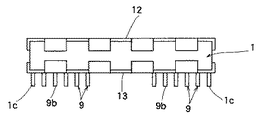
従来の電子回路ユニットの図面を説明すると、図7は従来の電子回路ユニットを示す分解斜視図である。 FIG. 7 is an exploded perspective view showing a conventional electronic circuit unit.
次に、従来の電子回路ユニットの構成を図7に基づいて説明すると、金属板からなる箱形(ロ字状)の枠体51は、両側に設けられた開放部51a、51bと、ロ字状のそれぞれの四辺に設けられた舌片51cと、4角の近傍から下方に突出する複数個の取付足51dを有する。
Next, a configuration of a conventional electronic circuit unit will be described with reference to FIG. 7. A box-shaped (b-shaped)
金属板からなるシールド板52は、枠体51内に配置されて、枠体51内が複数個の区画室に区画される。
The
絶縁基板からなる回路基板53は、外周縁に複数個の切り欠き部53aを有すると共に、表裏の両面には、配線用の導電パターン(図示せず)が設けられ、この回路基板53には、カバー付電子部品54や、コイル等の電子部品55が搭載されて、所望の電気回路が形成されている。
The
複数個の線状の端子56は、回路基板53の一辺の近傍で、回路基板53に貫通して配置され、導電パターンに半田付け(図示せず)されて取り付けられている。
この複数個の端子56は、一列状態で等間隔に配設され、回路基板53の下方から突出する部分が端子部56aとなると共に、回路基板53の上方から突出する部分が抜け止め部56bとなっている。
The plurality of
The plurality of
そして、回路基板53は、枠体51内に収納され、舌片51cが切り欠き部53a側に折り曲げられ、導電パターンと舌片51cが半田付けされて、回路基板53が枠体51に取り付けられる。
Then, the
金属板からなる第1のカバー(上カバー)57と第2のカバー(下カバー)58のそれぞれは、枠体51の開放部51a、51bを覆った状態で、枠体51に取り付けられる。
この時、端子56の端子部56aは、第2のカバー58の孔58aから下方に突出した状態となっている。(例えば、特許文献1参照)
Each of the first cover (upper cover) 57 and the second cover (lower cover) 58 made of a metal plate is attached to the
At this time, the
このような構成を有する従来の電子回路ユニットは、複数個の端子56が一列状態で配置されると共に、カバー付電子部品54が端子56列外に配置されるため、回路基板53は、幅方向に大きくなる。
また、複数個の端子56は、それぞれ個々に取り付けせねばならず、作業性が悪くなる。
In the conventional electronic circuit unit having such a configuration, since the plurality of
In addition, the plurality of
従来の電子回路ユニットは、複数個の端子56が一列状態で配置されると共に、カバー付電子部品54が端子56列外に配置されるため、回路基板53は、幅方向に大きくなり、大型になるという問題がある。
また、複数個の端子56は、それぞれ個々に取り付けせねばならず、作業性が悪くなり、生産性が悪いという問題がある。
In the conventional electronic circuit unit, since the plurality of
In addition, the plurality of
そこで、本発明は小型化に適し、生産性の良好な電子回路ユニットを提供することを目的とする。 Accordingly, an object of the present invention is to provide an electronic circuit unit that is suitable for miniaturization and has good productivity.
上記課題を解決するための第1の解決手段として、金属板からなる箱形の枠体と、この枠体内に取り付けられた回路基板と、この回路基板に搭載された金属製カバー付電子部品と、前記回路基板に貫通した状態で取り付けられた複数個の線状の端子とを備え、前記端子は、複数個が互いに間隔を持って少なくとも一列に配置された第1,第2の端子群を構成し、前記第1,第2の端子群は、一列状態で、前記回路基板の一辺の近傍に配置されると共に、前記第1,第2の端子群間には、空隙部が設けられ、前記金属製カバー付電子部品が、前記空隙部に、前記金属製カバー付電子部品の長手方向に前記金属製カバー付電子部品と前記第1、第2の端子群が一直線になるように位置した状態で、前記回路基板に配設された構成とした。 As a first means for solving the above problems, a box-shaped frame made of a metal plate, a circuit board mounted in the frame, and an electronic component with a metal cover mounted on the circuit board, A plurality of linear terminals attached in a state of penetrating the circuit board, wherein the terminals include first and second terminal groups arranged at least in a row at intervals from each other. configured, the first, the second terminal group is a single row state, while being arranged in the vicinity of one side of the circuit board, the first, between the second terminal group, the void portion is provided, The electronic component with a metal cover is positioned in the gap so that the electronic component with a metal cover and the first and second terminal groups are in a straight line in the longitudinal direction of the electronic component with the metal cover. In this state, the circuit board is arranged on the circuit board.
また、第2の解決手段として、前記カバー付電子部品は水晶発振器で構成された。
また、第3の解決手段として、絶縁材からなる支持体を有し、前記端子は、一端側が前記支持体で支持されると共に、前記支持体と前記カバー付電子部品は、前記回路基板の同一面側に配置された構成とした。
また、第4の解決手段として、前記支持体は、前記第1,第2の端子群のそれぞれで一体化された構成とした。
As a second solution, the cover-equipped electronic component is composed of a crystal oscillator.
As a third solution, the terminal has a support made of an insulating material, and the terminal is supported at one end by the support, and the support and the electronic component with cover are the same as the circuit board. It was set as the structure arrange | positioned at the surface side.
As a fourth solution, the support is integrated with each of the first and second terminal groups.
また、第5の解決手段として、前記枠体内は、シールド板によって複数の区画室に区画されると共に、受信したテレビジョン信号を中間周波信号に周波数変換するチューナ回路部と、前記中間周波信号を検波して映像信号と音声信号とを出力する復調回路部とが前記シールド板を挟んで隣り合う前記区画室に配置され、前記チューナ回路部に設けられたPLL用ICと、前記復調回路部に設けられた復調用ICが前記水晶発振器に接続された構成とした。
また、第6の解決手段として、前記水晶発振器が前記チューナ回路部と前記復調回路部との間に設けられた前記シールド板の隣りに位置する前記チューナ回路部側の前記区画室に収納された構成とした。
As a fifth solution, the frame is partitioned into a plurality of compartments by a shield plate, a tuner circuit unit that converts a received television signal into an intermediate frequency signal, and the intermediate frequency signal. A demodulation circuit unit that detects and outputs a video signal and an audio signal is disposed in the adjacent compartment with the shield plate interposed therebetween, and a PLL IC provided in the tuner circuit unit, and a demodulation circuit unit The provided demodulating IC is connected to the crystal oscillator.
As a sixth solution, the crystal oscillator is housed in the compartment on the tuner circuit portion side located next to the shield plate provided between the tuner circuit portion and the demodulation circuit portion. The configuration.
本発明の電子回路ユニットは、金属板からなる箱形の枠体と、この枠体内に取り付けられた回路基板と、この回路基板に搭載された金属製カバー付電子部品と、前記回路基板に貫通した状態で取り付けられた複数個の線状の端子とを備え、前記端子は、複数個が互いに間隔を持って少なくとも一列に配置された第1,第2の端子群を構成し、前記第1,第2の端子群は、一列状態で、前記回路基板の一辺の近傍に配置されると共に、前記第1,第2の端子群間には、空隙部が設けられ、前記金属製カバー付電子部品が、前記空隙部に、前記金属製カバー付電子部品の長手方向に前記金属製カバー付電子部品と前記第1、第2の端子群が一直線になるように位置した状態で、前記回路基板に配設されたため、カバー付電子部品の配置のスペースファクタが良く、従って、回路基板の幅方向の寸法を小さくできて、小型のものが得られる。 An electronic circuit unit according to the present invention includes a box-shaped frame body made of a metal plate, a circuit board mounted in the frame body, an electronic component with a metal cover mounted on the circuit board, and the circuit board. with the a plurality of linear terminals mounted in the state, the terminal may first plurality are arranged in at least one row with a distance from each other, constitute the second terminal group, said first The second terminal group is arranged in a row and in the vicinity of one side of the circuit board, and a gap is provided between the first and second terminal groups, and the metal cover-equipped electronic device The circuit board in a state where the component is positioned in the gap so that the metal part with electronic cover and the first and second terminal groups are aligned in the longitudinal direction of the electronic part with metal cover. Because of the placement space for the electronic parts with cover Akuta good, therefore, it is possible to reduce the widthwise dimension of the circuit board, a small size is obtained.
また、カバー付電子部品は水晶発振器で構成されたため、特に、テレビチューナに使用して好適となる。 Further, since the electronic component with cover is composed of a crystal oscillator, it is particularly suitable for use in a television tuner.
また、絶縁材からなる支持体を有し、端子は、一端側が支持体で支持されると共に、支持体とカバー付電子部品は、回路基板の同一面側に配置されたため、カバー付電子部品のカバーと端子との間の絶縁性を高めることが出来る。 In addition, the terminal has a support made of an insulating material, and the terminal is supported by the support at one end, and the support and the electronic component with the cover are arranged on the same surface side of the circuit board. The insulation between the cover and the terminal can be enhanced.
また、支持体は、第1,第2の端子群のそれぞれで一体化されたため、回路基板への端子の取付が容易となって、生産性の良好なものが得られる。 In addition, since the support is integrated in each of the first and second terminal groups, it is easy to attach the terminals to the circuit board, and a product with good productivity can be obtained.
また、枠体内は、シールド板によって複数の区画室に区画されると共に、受信したテレビジョン信号を中間周波信号に周波数変換するチューナ回路部と、中間周波信号を検波して映像信号と音声信号とを出力する復調回路部とがシールド板を挟んで隣り合う区画室に配置され、チューナ回路部に設けられたPLL用ICと、復調回路部に設けられた復調用ICが水晶発振器に接続されたため、一つの水晶発振器をチューナ回路部と復調回路部に兼用できて、コンパクトなものが得られる。 The frame body is partitioned into a plurality of compartments by a shield plate, a tuner circuit unit that converts the received television signal into an intermediate frequency signal, a video signal and an audio signal by detecting the intermediate frequency signal Is placed in the adjacent compartment with the shield plate interposed therebetween, and the PLL IC provided in the tuner circuit part and the demodulation IC provided in the demodulation circuit part are connected to the crystal oscillator. A single crystal oscillator can be used for both the tuner circuit and the demodulation circuit, and a compact one can be obtained.
また、水晶発振器がチューナ回路部と復調回路部との間に設けられたシールド板の隣りに位置するチューナ回路部側の区画室に収納されたため、水晶発振器がPLL用ICと復調用ICに短い状態で接続することができる。 In addition, since the crystal oscillator is housed in the compartment on the tuner circuit unit side located next to the shield plate provided between the tuner circuit unit and the demodulation circuit unit, the crystal oscillator is short to the PLL IC and the demodulation IC. Can be connected in a state.
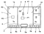
本発明の電子回路ユニットの図面を説明すると、図1は本発明の電子回路ユニットを示す正面図、図2は本発明の電子回路ユニットに係り、カバーを取り去った状態の平面図、図3は本発明の電子回路ユニットに係り、カバーを取り去った状態の下面図である。 FIG. 1 is a front view showing the electronic circuit unit of the present invention, FIG. 2 is a plan view of the electronic circuit unit of the present invention, with the cover removed, and FIG. FIG. 4 is a bottom view of the electronic circuit unit of the present invention in a state where a cover is removed.
また、図4は本発明の電子回路ユニットに係り、カバーを取り去った状態で一部を切り欠いた斜視図、図5は本発明の電子回路ユニットの要部の拡大断面図、図6は本発明の電子回路ユニットに係り、端子部材を裏返した状態の斜視図である。 FIG. 4 relates to the electronic circuit unit of the present invention, and is a perspective view with a part cut away with the cover removed, FIG. 5 is an enlarged cross-sectional view of the main part of the electronic circuit unit of the present invention, and FIG. FIG. 5 is a perspective view of the electronic circuit unit of the invention, with the terminal member turned upside down.
次に、本発明の電子回路ユニットの構成を図1〜図6に基づいて説明すると、
金属板からなる箱形(ロ字状)の枠体1は、両側に設けられた開放部1a、1bと、4角の近傍から下方に突出する複数個の取付足1cを有する。
Next, the configuration of the electronic circuit unit of the present invention will be described with reference to FIGS.
A box-shaped (b-shaped)
金属板からなるシールド板2は、枠体1内に配置されて、枠体1内が複数個の区画室S1,S2に区画される。
The
セラミック基板等からなる四角形の回路基板3は、その表裏の両面に、配線用の導電パターン4が設けられ、この回路基板3には、水晶発振器等からなり、金属製カバー等が設けられたカバー付電子部品5、PLL用ICP1,復調用ICP2や、コイル、チップ抵抗等の電子部品6が搭載されて、所望の電気回路が形成されている。
A
即ち、回路基板3には、受信したテレビジョン信号を中間周波信号に周波数変換するチューナ回路部K1と、中間周波信号を検波して映像信号と音声信号とを出力する復調回路部K2とが設けられると共に、シールド板2を挟んで隣り合う区画室S1には、チューナ回路部K1が配置され、また、区画室S2には、復調回路部K2が配置されている。
That is, the
また、チューナ回路部K1には、PLL用ICP1が設けられると共に、復調回路部K2には、復調用ICP2が設けられ、水晶発振器であるカバー付電子部品5は、PLL用ICP1と復調用ICP2に接続されている。 The tuner circuit unit K1 is provided with a PLL ICP1, the demodulation circuit unit K2 is provided with a demodulation ICP2, and the electronic component with cover 5 that is a crystal oscillator is connected to the PLL ICP1 and the demodulation ICP2. It is connected.
そして、水晶発振器であるカバー付電子部品5がチューナ回路部K1と復調回路部K2との間に設けられたシールド板2の隣りに位置するチューナ回路部K1側の区画室S1に収納されたため、カバー付電子部品5がPLL用ICP1と復調用ICP2に短い状態で接続することができる。
Since the cover-equipped electronic component 5 that is a crystal oscillator is housed in the compartment S1 on the tuner circuit unit K1 side that is located next to the
端子部材7は、特に、図5,図6に示すように、セラミック材等の絶縁材からなる複数個の支持体8と、金属線(線状)からなる複数個の端子9とで構成されている。
そして、複数個の支持体8は、一列状態で一体化されると共に、複数個の端子9は、一端部9aがそれぞれが支持体8の下部中央部に埋設されて支持され、他端部の端子部9bが下方に突出した状態となっている。
As shown in FIGS. 5 and 6, the
The plurality of
また、それぞれの支持体8は、下部側において、それぞれの端子9の周囲に設けられた十字状の空洞部8aと、空洞部8aを形成するための下方に突出した突部8bと、隣り合う支持部8間の外周部に設けられた切り溝8cを有する。
Further, each
なお、この実施例の空洞部8aは、十字状で形成されているが、円形状や矩形状等でも良い。
In addition, although the
また、端子部材7は、複数個の支持体8(ここでは5個)と、それぞれの支持体8に取り付けられた複数個の端子9(ここでは5個)によって構成される第1,第2の端子群7a、7bを有している。
The
この第1,第2の端子群7a、7bは、多数の端子9が一列状に埋設(取付)され、且つ、多数の支持体8が一列状に一体化された状態で、支持体8が所望の個数の箇所の切り溝8cに沿って切断することによって、製造されるようになっている。
In the first and second
そして、このような構成を有する第1,第2の端子群7a、7bは、一列状態で、回路基板3の一辺の近傍に配置されると共に、第1,第2の端子群7a、7b間には、空隙部10が形成された状態となる。
The first and second
この時、支持体8の突部8bは、回路基板3の上面に当接すると共に、端子部9bが回路基板3の孔3aを貫通して下方に突出した状態となる。
また、突部8bが回路基板3の上面に当接した際、回路基板3の上面に位置する端子9の周囲には、空洞部8aが存在した状態となる。
At this time, the
Further, when the
そして、端子9の端子部9bは、回路基板3の下面に設けられた導電パターン4に半田11付けして接続、固定される。
また、この半田11付け方法は、先ず、回路基板3の下面の導電パターン4上にクリーム半田(図示せず)を塗布した状態で、第1,第2の端子群7a、7bの端子9を、回路基板3の上面側から孔3aに貫通する。
The
In addition, in this soldering method, first, the
次に、この状態で、リフロー炉内に搬送し、クリーム半田を溶融して、半田11付が行われるが、この時、溶融された半田11は、毛細管現象により孔3aを通って回路基板3の上面側に流出する。
そして、回路基板3の上面に流出した半田11は、空洞部8a内に位置するため、上面に流出した半田11によって、支持体8が上方に持ち上げ(浮き状態)られることが無くなり、精度の良い、端子部材7の取付が出来る。
Next, in this state, it is transported into a reflow furnace, the cream solder is melted, and the
Since the
なお、この実施例では、複数個の支持体8が一体化されたもので説明したが、個々の支持体8が複数個一列状に配列されたものでも良い。
In this embodiment has been described in what plurality of
また、前述のカバー付電子部品5は、本体部を覆う鍔付のカバー5aと、本体部から下方に突出する引出部(端子)5bを有し、このカバー付電子部品5は、第1,第2の端子群7a、7b間の空隙部10内にカバー5aを配置した状態で、引出部5bが孔3aを貫通して、引出部5bが回路基板3の下面に設けられた導電パターン4に半田付けされる。
The electronic component 5 with a cover includes a
そして、このカバー付電子部品5の半田付方法は、前述した端子部材7の半田付方法と同様であり、カバー付電子部品5と端子部材7の半田付は、リフロー炉に搬送されて、同時に行われるものである。
And the soldering method of this electronic component 5 with a cover is the same as the soldering method of the
このように、カバー付電子部品5が空隙部10内に配設されることによって、回路基板3の幅方向の寸法を小さくできると共に、カバー5aの近傍には、端子部材7の絶縁材の支持体8が位置することによって、カバー5aと端子9との間の絶縁性を高めることが出来る。
As described above, the electronic component 5 with the cover is disposed in the
そして、回路基板3は、枠体1内に収納され、適宜手段によって、枠体1内に取り付けられる。
この時、この実施例では、第1の端子群7aの大部分が復調回路部K2を設けた区画室S2側に配置され、第2の端子群7bの全体がチューナ回路部K1を設けた区画室S1に配置された状態となっていると共に、カバー付電子部品5が第1,第2の端子群7a、7b間の位置で、チューナ回路部K1を設けた区画室S1に収納された状態となっている。
And the
At this time, in this embodiment, most of the first
金属板からなる第1のカバー(上カバー)12と第2のカバー(下カバー)13のそれぞれは、枠体1の開放部1a、1bを覆った状態で、枠体1に取り付けられる。
この時、端子9の端子部9bは、ここでは図示しないが、第2のカバー13の孔から下方に突出した状態となっている。
Each of the first cover (upper cover) 12 and the second cover (lower cover) 13 made of a metal plate is attached to the
At this time, the
1:枠体
1a:開放部
1b:開放部
1c:取付足
2:シールド板
3:回路基板
3a:孔
4:導電パターン
5:カバー付電子部品
5a:カバー
5b:引出部
6:電子部品
7:端子部材
8:支持体
8a:空洞部
8b:突部
8c:切り溝
9:端子
9a:一端部
9b:端子部
10:空隙部
11:半田
12:第1のカバー(上カバー)
13: 第2のカバー(下カバー)
S1: 区画室
S2: 区画室
K1: チューナ回路部
K2: 復調回路部
P1: PLL用IC
P2: 復調用IC
1:
13: Second cover (lower cover)
S1: compartment S2: compartment K1: tuner circuit K2: demodulation circuit P1: PLL IC
P2: Demodulation IC
Claims (6)
6. The crystal oscillator according to claim 5, wherein the crystal oscillator is housed in the compartment on the tuner circuit portion side located next to the shield plate provided between the tuner circuit portion and the demodulation circuit portion. Electronic circuit unit.
Priority Applications (5)
| Application Number | Priority Date | Filing Date | Title |
|---|---|---|---|
| JP2003313910A JP4170862B2 (en) | 2003-09-05 | 2003-09-05 | Electronic circuit unit |
| KR1020040057457A KR100586902B1 (en) | 2003-09-05 | 2004-07-23 | Electronic circuit unit |
| US10/932,953 US7106085B2 (en) | 2003-09-05 | 2004-09-02 | Electronic circuit unit having small size and good productivity |
| EP04020884A EP1513384A3 (en) | 2003-09-05 | 2004-09-02 | Electronic circuit unit having small size and good productivity |
| CNB2004100687316A CN100379326C (en) | 2003-09-05 | 2004-09-06 | Electronic circuit unit |
Applications Claiming Priority (1)
| Application Number | Priority Date | Filing Date | Title |
|---|---|---|---|
| JP2003313910A JP4170862B2 (en) | 2003-09-05 | 2003-09-05 | Electronic circuit unit |
Publications (2)
| Publication Number | Publication Date |
|---|---|
| JP2005085863A JP2005085863A (en) | 2005-03-31 |
| JP4170862B2 true JP4170862B2 (en) | 2008-10-22 |
Family
ID=34131897
Family Applications (1)
| Application Number | Title | Priority Date | Filing Date |
|---|---|---|---|
| JP2003313910A Expired - Fee Related JP4170862B2 (en) | 2003-09-05 | 2003-09-05 | Electronic circuit unit |
Country Status (5)
| Country | Link |
|---|---|
| US (1) | US7106085B2 (en) |
| EP (1) | EP1513384A3 (en) |
| JP (1) | JP4170862B2 (en) |
| KR (1) | KR100586902B1 (en) |
| CN (1) | CN100379326C (en) |
Families Citing this family (7)
| Publication number | Priority date | Publication date | Assignee | Title |
|---|---|---|---|---|
| JP2006311161A (en) * | 2005-04-28 | 2006-11-09 | Denso Corp | Wireless transceiver and method for manufacturing the same |
| KR100716826B1 (en) * | 2005-05-10 | 2007-05-09 | 삼성전기주식회사 | Manufacturing method of printed circuit board with embedded Electronic Component |
| JP2007267172A (en) | 2006-03-29 | 2007-10-11 | Alps Electric Co Ltd | Tuner for digital broadcasting, and digital broadcast receiving apparatus using same |
| KR100829755B1 (en) | 2007-03-02 | 2008-05-15 | 삼성에스디아이 주식회사 | Chassis base assembly and display apparatus comprising the same |
| CN102099538B (en) * | 2008-07-15 | 2013-08-14 | 西门子公司 | Method for the assembly of a tower and tower |
| TWM429683U (en) * | 2012-01-06 | 2012-05-21 | Bothhand Entpr Inc | Packaging case of electronic device |
| JP5984526B2 (en) | 2012-06-20 | 2016-09-06 | 日本電波工業株式会社 | Surface mount device |
Family Cites Families (21)
| Publication number | Priority date | Publication date | Assignee | Title |
|---|---|---|---|---|
| US4306205A (en) * | 1978-10-31 | 1981-12-15 | Murata Manufacturing Co., Ltd. | High frequency apparatus |
| CH687276A5 (en) * | 1989-01-23 | 1996-10-31 | Balzers Hochvakuum | Tuning fork quartz manometer. |
| JP3176963B2 (en) * | 1991-08-30 | 2001-06-18 | 新潟精密株式会社 | High frequency clock circuit |
| JPH08222827A (en) * | 1995-02-14 | 1996-08-30 | Daishinku Co | Insulating plate for electronic component |
| WO1997002596A1 (en) * | 1995-06-30 | 1997-01-23 | Kabushiki Kaisha Toshiba | Electronic component and method of production thereof |
| DE19636181A1 (en) * | 1996-09-06 | 1998-03-12 | Philips Patentverwaltung | RF module, e.g. B. Tuner |
| JP3333811B2 (en) * | 1996-10-25 | 2002-10-15 | アルプス電気株式会社 | Manufacturing method of high frequency equipment |
| JP3179719B2 (en) * | 1996-11-20 | 2001-06-25 | アルプス電気株式会社 | Electronics |
| JPH11136152A (en) * | 1997-10-31 | 1999-05-21 | Alps Electric Co Ltd | Digital television signal reception tuner |
| JP4379932B2 (en) * | 1998-09-18 | 2009-12-09 | エプソントヨコム株式会社 | Crystal oscillator |
| JP2000165086A (en) * | 1998-11-30 | 2000-06-16 | Kinseki Ltd | Electronic component case |
| JP3062909U (en) * | 1999-04-08 | 1999-10-15 | 船井電機株式会社 | Tuner unit |
| JP2001177044A (en) * | 1999-12-15 | 2001-06-29 | Murata Mfg Co Ltd | Electronic part module and piezoelectric oscillator |
| JP3729708B2 (en) | 2000-06-19 | 2005-12-21 | シャープ株式会社 | Electronics |
| JP4701505B2 (en) * | 2001-01-29 | 2011-06-15 | パナソニック株式会社 | Inertial transducer |
| US6774641B2 (en) * | 2001-06-20 | 2004-08-10 | Nec Corporation | Printed circuit board design support apparatus, method, and program |
| US6846998B2 (en) * | 2002-01-28 | 2005-01-25 | Citizen Watch Co., Ltd. | Switch connecting structure for timepiece |
| JP2003218259A (en) * | 2002-01-28 | 2003-07-31 | Tokyo Denpa Co Ltd | Electronic component container |
| JP4051321B2 (en) * | 2002-06-27 | 2008-02-20 | 京セラ株式会社 | Manufacturing method of electronic component device |
| JP2004312285A (en) * | 2003-04-04 | 2004-11-04 | Toyo Commun Equip Co Ltd | Surface mounted piezoelectric oscillator |
| JP2005235806A (en) * | 2004-02-17 | 2005-09-02 | Toyo Commun Equip Co Ltd | Electronic component with case |
-
2003
- 2003-09-05 JP JP2003313910A patent/JP4170862B2/en not_active Expired - Fee Related
-
2004
- 2004-07-23 KR KR1020040057457A patent/KR100586902B1/en not_active IP Right Cessation
- 2004-09-02 US US10/932,953 patent/US7106085B2/en not_active Expired - Fee Related
- 2004-09-02 EP EP04020884A patent/EP1513384A3/en not_active Withdrawn
- 2004-09-06 CN CNB2004100687316A patent/CN100379326C/en not_active Expired - Fee Related
Also Published As
| Publication number | Publication date |
|---|---|
| US7106085B2 (en) | 2006-09-12 |
| CN100379326C (en) | 2008-04-02 |
| EP1513384A3 (en) | 2008-12-31 |
| CN1592558A (en) | 2005-03-09 |
| EP1513384A2 (en) | 2005-03-09 |
| US20050052198A1 (en) | 2005-03-10 |
| JP2005085863A (en) | 2005-03-31 |
| KR100586902B1 (en) | 2006-06-08 |
| KR20050025241A (en) | 2005-03-14 |
Similar Documents
| Publication | Publication Date | Title |
|---|---|---|
| JP4984912B2 (en) | High frequency tuner module | |
| JP4170862B2 (en) | Electronic circuit unit | |
| JP2010213255A (en) | Crystal oscillator with pedestal | |
| US9241418B2 (en) | Surface mount device | |
| JP2006260842A (en) | Terminal mounting structure and its terminal mounting method | |
| JPH10313157A (en) | Printed board | |
| JP2006237137A (en) | Electronic circuit unit | |
| JP2008112832A (en) | High-frequency unit, and manufacturing method of high-frequency unit | |
| JP2570336B2 (en) | Hybrid integrated circuit device | |
| JP4571012B2 (en) | Crystal unit with pedestal | |
| JP2002299879A (en) | Electronic component manufacturing method | |
| JP7050718B2 (en) | Positioning jig for soldering | |
| JP2006179523A (en) | High-frequency module | |
| JP2005203521A (en) | Electronic device and intermediate product thereof | |
| JP2003124745A (en) | Structure and production method for electronic component | |
| JP3898164B2 (en) | High frequency circuit unit and manufacturing method thereof | |
| JPH0738228A (en) | Wiring board | |
| JP2004342713A (en) | Electronic circuit unit and its manufacturing method | |
| JP4580884B2 (en) | Connection structure of circuit board and frame | |
| JP2881264B2 (en) | Electronic component mounting board with mounting recess | |
| JP2007267172A (en) | Tuner for digital broadcasting, and digital broadcast receiving apparatus using same | |
| JP2003318297A (en) | Electronic component device | |
| JP2006108909A (en) | Seating for electron device | |
| JP2020102496A (en) | Mass production method for chip element mounting board module, relay board, block, and module | |
| JP2005129656A (en) | Surface-mounting electronic circuit unit |
Legal Events
| Date | Code | Title | Description |
|---|---|---|---|
| A621 | Written request for application examination |
Free format text: JAPANESE INTERMEDIATE CODE: A621 Effective date: 20060303 |
|
| A977 | Report on retrieval |
Free format text: JAPANESE INTERMEDIATE CODE: A971007 Effective date: 20080212 |
|
| A131 | Notification of reasons for refusal |
Free format text: JAPANESE INTERMEDIATE CODE: A131 Effective date: 20080219 |
|
| A521 | Request for written amendment filed |
Free format text: JAPANESE INTERMEDIATE CODE: A523 Effective date: 20080327 |
|
| TRDD | Decision of grant or rejection written | ||
| A01 | Written decision to grant a patent or to grant a registration (utility model) |
Free format text: JAPANESE INTERMEDIATE CODE: A01 Effective date: 20080729 |
|
| A01 | Written decision to grant a patent or to grant a registration (utility model) |
Free format text: JAPANESE INTERMEDIATE CODE: A01 |
|
| A61 | First payment of annual fees (during grant procedure) |
Free format text: JAPANESE INTERMEDIATE CODE: A61 Effective date: 20080807 |
|
| FPAY | Renewal fee payment (event date is renewal date of database) |
Free format text: PAYMENT UNTIL: 20110815 Year of fee payment: 3 |
|
| FPAY | Renewal fee payment (event date is renewal date of database) |
Free format text: PAYMENT UNTIL: 20110815 Year of fee payment: 3 |
|
| LAPS | Cancellation because of no payment of annual fees |