JP4162890B2 - Liquid crystal display - Google Patents
Liquid crystal display Download PDFInfo
- Publication number
- JP4162890B2 JP4162890B2 JP2001396509A JP2001396509A JP4162890B2 JP 4162890 B2 JP4162890 B2 JP 4162890B2 JP 2001396509 A JP2001396509 A JP 2001396509A JP 2001396509 A JP2001396509 A JP 2001396509A JP 4162890 B2 JP4162890 B2 JP 4162890B2
- Authority
- JP
- Japan
- Prior art keywords
- signal line
- liquid crystal
- counter
- voltage signal
- electrode
- Prior art date
- Legal status (The legal status is an assumption and is not a legal conclusion. Google has not performed a legal analysis and makes no representation as to the accuracy of the status listed.)
- Expired - Fee Related
Links
Images


Classifications
-
- G—PHYSICS
- G02—OPTICS
- G02F—OPTICAL DEVICES OR ARRANGEMENTS FOR THE CONTROL OF LIGHT BY MODIFICATION OF THE OPTICAL PROPERTIES OF THE MEDIA OF THE ELEMENTS INVOLVED THEREIN; NON-LINEAR OPTICS; FREQUENCY-CHANGING OF LIGHT; OPTICAL LOGIC ELEMENTS; OPTICAL ANALOGUE/DIGITAL CONVERTERS
- G02F1/00—Devices or arrangements for the control of the intensity, colour, phase, polarisation or direction of light arriving from an independent light source, e.g. switching, gating or modulating; Non-linear optics
- G02F1/01—Devices or arrangements for the control of the intensity, colour, phase, polarisation or direction of light arriving from an independent light source, e.g. switching, gating or modulating; Non-linear optics for the control of the intensity, phase, polarisation or colour
- G02F1/13—Devices or arrangements for the control of the intensity, colour, phase, polarisation or direction of light arriving from an independent light source, e.g. switching, gating or modulating; Non-linear optics for the control of the intensity, phase, polarisation or colour based on liquid crystals, e.g. single liquid crystal display cells
- G02F1/133—Constructional arrangements; Operation of liquid crystal cells; Circuit arrangements
- G02F1/1333—Constructional arrangements; Manufacturing methods
- G02F1/1343—Electrodes
- G02F1/134309—Electrodes characterised by their geometrical arrangement
- G02F1/134363—Electrodes characterised by their geometrical arrangement for applying an electric field parallel to the substrate, i.e. in-plane switching [IPS]
-
- G—PHYSICS
- G02—OPTICS
- G02F—OPTICAL DEVICES OR ARRANGEMENTS FOR THE CONTROL OF LIGHT BY MODIFICATION OF THE OPTICAL PROPERTIES OF THE MEDIA OF THE ELEMENTS INVOLVED THEREIN; NON-LINEAR OPTICS; FREQUENCY-CHANGING OF LIGHT; OPTICAL LOGIC ELEMENTS; OPTICAL ANALOGUE/DIGITAL CONVERTERS
- G02F1/00—Devices or arrangements for the control of the intensity, colour, phase, polarisation or direction of light arriving from an independent light source, e.g. switching, gating or modulating; Non-linear optics
- G02F1/01—Devices or arrangements for the control of the intensity, colour, phase, polarisation or direction of light arriving from an independent light source, e.g. switching, gating or modulating; Non-linear optics for the control of the intensity, phase, polarisation or colour
- G02F1/13—Devices or arrangements for the control of the intensity, colour, phase, polarisation or direction of light arriving from an independent light source, e.g. switching, gating or modulating; Non-linear optics for the control of the intensity, phase, polarisation or colour based on liquid crystals, e.g. single liquid crystal display cells
- G02F1/133—Constructional arrangements; Operation of liquid crystal cells; Circuit arrangements
- G02F1/1333—Constructional arrangements; Manufacturing methods
- G02F1/1343—Electrodes
-
- G—PHYSICS
- G02—OPTICS
- G02F—OPTICAL DEVICES OR ARRANGEMENTS FOR THE CONTROL OF LIGHT BY MODIFICATION OF THE OPTICAL PROPERTIES OF THE MEDIA OF THE ELEMENTS INVOLVED THEREIN; NON-LINEAR OPTICS; FREQUENCY-CHANGING OF LIGHT; OPTICAL LOGIC ELEMENTS; OPTICAL ANALOGUE/DIGITAL CONVERTERS
- G02F1/00—Devices or arrangements for the control of the intensity, colour, phase, polarisation or direction of light arriving from an independent light source, e.g. switching, gating or modulating; Non-linear optics
- G02F1/01—Devices or arrangements for the control of the intensity, colour, phase, polarisation or direction of light arriving from an independent light source, e.g. switching, gating or modulating; Non-linear optics for the control of the intensity, phase, polarisation or colour
- G02F1/13—Devices or arrangements for the control of the intensity, colour, phase, polarisation or direction of light arriving from an independent light source, e.g. switching, gating or modulating; Non-linear optics for the control of the intensity, phase, polarisation or colour based on liquid crystals, e.g. single liquid crystal display cells
- G02F1/133—Constructional arrangements; Operation of liquid crystal cells; Circuit arrangements
- G02F1/136—Liquid crystal cells structurally associated with a semi-conducting layer or substrate, e.g. cells forming part of an integrated circuit
- G02F1/1362—Active matrix addressed cells
-
- G—PHYSICS
- G02—OPTICS
- G02F—OPTICAL DEVICES OR ARRANGEMENTS FOR THE CONTROL OF LIGHT BY MODIFICATION OF THE OPTICAL PROPERTIES OF THE MEDIA OF THE ELEMENTS INVOLVED THEREIN; NON-LINEAR OPTICS; FREQUENCY-CHANGING OF LIGHT; OPTICAL LOGIC ELEMENTS; OPTICAL ANALOGUE/DIGITAL CONVERTERS
- G02F2201/00—Constructional arrangements not provided for in groups G02F1/00 - G02F7/00
- G02F2201/12—Constructional arrangements not provided for in groups G02F1/00 - G02F7/00 electrode
- G02F2201/122—Constructional arrangements not provided for in groups G02F1/00 - G02F7/00 electrode having a particular pattern
Description
【0001】
【発明の属する技術分野】
本発明は液晶表示装置に係り、特に横電界方式と称される液晶表示装置に関する。
【0002】
【従来の技術】
横電界方式と称される液晶表示装置は、液晶を介して対向配置される各基板の一方の基板の液晶側の面の画素領域に画素電極とこの画素電極との間に電界を発生せしめる対向電極とを備え、該電界のうち基板とほぼ平行な成分によって液晶を挙動させる構成となっている。
【0003】
そして、このような構成をアクティブマトリクス型のものに適用させたものは、まず、前記一方の基板の液晶側の面に、並設された複数のゲート信号線とこれら各ゲート信号線と交差するようにして並設された複数のドレイン信号線とで囲まれた各領域を前記画素領域としている。
【0004】
そして、これら各画素領域に、ゲート信号線からの走査信号によって作動する薄膜トランジスタと、この薄膜トランジスタを介してドレイン信号線からの映像信号が供給される前記画素電極と、該映像信号に対して基準となる信号が供給される前記対向電極とが備えられている。
【0005】
ここで、画素電極と対向電極はそれぞれ一方向に延在する帯状のパターンとして形成され、それら各電極は2個あるいはそれ以上の個数で形成して交互に配置させるのが通常である。
【0006】
また、このような構成において、対向電極をドレイン信号線をも被って形成される絶縁膜の上面に形成させるとともに、該ドレイン信号線とその中心軸をほぼ一致させ該ドレイン信号線の幅よりも大きな幅を有して該ドレイン信号線に沿って形成された構成のものも知られている。
【0007】
ドレイン信号線からの電気力線がその上方の対向電極に終端させやすくし、画素電極に終端させるのを防止するためである。画素電極に該電気力線が終端するとそれがノイズとなってしまうからである。
【0008】
【発明が解決しようとする課題】
しかしながら、このような構成からなる液晶表示装置は、対向電極に信号を供給する対向電圧信号線を必要とし、それが画素領域内を走行して配置させるために画素領域のいわゆる開口率を向上させる妨げとなっていたという不都合があった。
【0009】
また、対向電極と対向電圧信号線は絶縁層を介して配置されることが多く、それらの電気的接続は該絶縁層に形成した小さなスルーホールを通して行なうため、該接続のさらなる信頼性が望まれていた。近年における高精細化の傾向に伴うものである。
【0010】
本発明は、このような事情に基づいてなされたもので、その目的は画素領域の開口率を向上させた液晶表示装置を提供することにある。
【0011】
また、本発明の他の目的は、対向電極と対向電圧信号線の信頼性ある接続を図った液晶表示装置を提供することにある。
【0012】
【課題を解決するための手段】
本願において開示される発明のうち、代表的なものの概要を簡単に説明すれば、以下のとおりである。
手段1.
本発明による液晶表示装置は、たとえば、液晶を介して対向配置される各基板のうち一方の基板の液晶側の面に、並設される複数のゲート信号線とこれらゲート信号線に交差して並設される複数のドレイン信号線とで囲まれた領域を画素領域とし、
これら各画素領域に、ゲート信号線からの走査信号によって作動されるスイッチング素子と、このスイッチング素子を介してドレイン信号線からの映像信号が供給される画素電極と、対向電圧信号線を介して前記映像信号に対して基準となる信号が供給される対向電極とが形成され、
前記対向電極は、複数の絶縁層の積層体の下層に形成され、
前記対向電圧信号線は、非透光性の導電体からなるとともに、前記複数の絶縁層の積層体の上層に形成され、前記ゲート信号線およびドレイン信号線をも被って格子状パターンをなし、その一部にて前記複数の絶縁層の積層体に形成されたスルーホールを通して前記対向電極に電気的に接続されていることを特徴とするものである。
【0013】
手段2.
本発明による液晶表示装置は、たとえば、手段1の構成を前提として、前記対向電圧信号線と対向電極との電気的接続は、前記複数の絶縁層の間に形成された画素電極を構成する導電層と同時に形成される他の導電層を介してなされていることを特徴とするものである。
【0014】
手段3.
本発明による液晶表示装置は、たとえば、手段1の構成を前提として、前記対向電圧信号線と対向電極との電気的接続は、前記複数の絶縁層の間に形成されたドレイン信号線を構成する導電層と同時に形成される他の導電層を介してなされていることを特徴とするものである。
【0015】
手段4.
本発明による液晶表示装置は、たとえば、手段1ないし3のうちいずれかの構成を前提として、前記対向電圧信号線と対向電極との電気的接続は2箇所あるいはそれ以上の個所でなされていることを特徴とするものである。
【0016】
手段5.
本発明による液晶表示装置は、たとえば、液晶を介して対向配置される各基板のうち一方の基板の液晶側の面に、並設される複数のゲート信号線とこれらゲート信号線に交差して並設される複数のドレイン信号線とで囲まれた領域を画素領域とし、
これら各画素領域に、ゲート信号線からの走査信号によって作動されるスイッチング素子と、このスイッチング素子を介してドレイン信号線からの映像信号が供給される画素電極と、対向電圧信号線を介して前記映像信号に対して基準となる信号が供給される対向電極とが形成され、
前記対向電極は複数の絶縁層の積層体の下層に形成され、前記画素電極は前記積層体の複数の絶縁層のうちの2つの絶縁層の間に形成され前記ドレイン信号線の延在方向に沿って延在され該方向に交差する方向に並設された複数の電極群からなるとともに、
前記対向電圧信号線は、非透光性の導電体からなるとともに、前記複数の絶縁層の積層体の上層に形成され、前記ゲート信号線およびドレイン信号線をも被って格子状パターンをなし、その一部にて前記複数の絶縁層の積層体に形成されたスルーホールを通して前記対向電極に電気的に接続されていることを特徴とするものである。
【0017】
手段6.
本発明による液晶表示装置は、たとえば、手段5の構成を前提として、画素領域を平面的に観た場合に、ドレイン信号線を被って形成された前記対向電圧信号線とそれに隣接して配置される画素電極との間の距離は、互いに隣接して配置される画素電極との間の距離よりも大きく設定されていることを特徴とするものである。
【0018】
手段7.
本発明による液晶表示装置は、たとえば、手段5、6のうちいずれかの構成を前提として、画素領域を平面的に観た場合に、ドレイン信号線を被って形成された前記対向電圧信号線とそれに隣接して配置される画素電極との間の距離は、該対向電圧信号線とそれに近接して配置される対向電極との間の距離よりも大きく設定されていることを特徴とするものである。
【0019】
手段8.
本発明による液晶表示装置は、たとえば、液晶を介して対向配置される各基板のうち一方の基板の液晶側の面に、並設される複数のゲート信号線とこれらゲート信号線に交差して並設される複数のドレイン信号線とで囲まれた領域を画素領域とし、
これら各画素領域に、ゲート信号線からの走査信号によって作動されるスイッチング素子と、このスイッチング素子を介してドレイン信号線からの映像信号が供給される画素電極と、対向電圧信号線を介して前記映像信号に対して基準となる信号が供給される対向電極とが形成され、
前記対向電圧信号線は、その表面が陽極化成されたAlあるいはその合金から構成されるとともに複数の絶縁層の積層体の下層に形成され、
前記対向電極は、透光性の導電体からなるとともに、前記複数の絶縁層の積層体の上層に形成され、前記ゲート信号線およびドレイン信号線をも被って格子状パターンをなし、その一部にて前記複数の絶縁層の積層体に形成されたスルーホールを通して前記対向電圧信号線に容量結合されていることを特徴とするものである。
【0020】
手段9.
本発明による液晶表示装置は、たとえば、液晶を介して対向配置される各基板のうち一方の基板の液晶側の面に、並設される複数のゲート信号線とこれらゲート信号線に交差して並設される複数のドレイン信号線とで囲まれた領域を画素領域とし、
これら各画素領域に、ゲート信号線からの走査信号によって作動されるスイッチング素子と、このスイッチング素子を介してドレイン信号線からの映像信号が供給される画素電極と、対向電圧信号線を介して前記映像信号に対して基準となる信号が供給される対向電極とが形成され、
前記対向電圧信号線は、その表面が陽極化成されたAlあるいはその合金から構成されるとともに複数の絶縁層の積層体の下層に形成され、かつこの対向電圧信号線の少なくとも一部の下層に該対向電圧信号線から露出された導電材料層を備え、
前記対向電極は、前記複数の絶縁層の積層体の上層に形成され、前記ゲート信号線およびドレイン信号線をも被って格子状パターンをなし、その一部にて前記複数の絶縁層の積層体に形成されたスルーホールを通して前記導電材料層に電気的に接続されていることを特徴とするものである。
【0021】
手段10.
本発明による液晶表示装置は、たとえば、手段9の構成を前提として、対向電極は透光性の導電層で構成されていることを特徴とするものである。
【0022】
手段11.
本発明による液晶表示装置は、たとえば、手段9、10のうちいずれかの構成を前提として、複数の絶縁層の前記積層体の2つの絶縁層の間にドレイン信号線が形成され、前記対向電極と導電材料層との間に前記ドレイン信号線の材料と同一の材料層が介在されていることを特徴とするものである。
【0023】
なお、本発明は以上の構成に限定されず、本発明の技術思想を逸脱しない範囲で種々の変更が可能である。
【0024】
【発明の実施の形態】
以下、本発明による液晶表示装置の実施例を図面を用いて説明をする。
実施例1.
《全体構成》
図2は、本発明による液晶表示装置の一実施例を示す全体構成図である。同図は等価回路図であるが、実際の幾何学的配置に対応させて描いている。
【0025】
同図において、液晶を介して互いに対向配置される一対の透明基板SUB1、SUB2があり、該液晶は一方の透明基板SUB1に対する他方の透明基板SUB2の固定を兼ねるシール材SLによって封入されている。
【0026】
シール材SLによって囲まれた前記一方の透明基板SUB1の液晶側の面には、そのx方向に延在しy方向に並設されたゲート信号線GLとy方向に延在しx方向に並設されたドレイン信号線DLとが形成されている。
【0027】
各ゲート信号線GLと各ドレイン信号線DLとで囲まれた領域は画素領域を構成するとともに、これら各画素領域のマトリクス状の集合体は液晶表示部ARを構成するようになっている。
【0028】
また、x方向に並設される各画素領域のそれぞれにはそれら各画素領域内に走行された共通の対向電圧信号線CLが形成されている。この対向電圧信号線CLは各画素領域の後述する対向電極CTに映像信号に対して基準となる電圧を供給するための信号線となるものである。
【0029】
各画素領域には、その片側のゲート信号線GLからの走査信号によって作動される薄膜トランジスタTFTと、この薄膜トランジスタTFTを介して片側のドレイン信号線DLからの映像信号が供給される画素電極PXが形成されている。
【0030】
この画素電極PXは、前記対向電圧信号線CLと接続された対向電極CTとの間に電界を発生させ、この電界によって液晶の光透過率を制御させるようになっている。
【0031】
前記ゲート信号線GLのそれぞれの一端は前記シール材SLを超えて延在され、その延在端は垂直走査駆動回路Vの出力端子が接続される端子を構成するようになっている。また、前記垂直走査駆動回路Vの入力端子は液晶表示パネルの外部に配置されたプリント基板からの信号が入力されるようになっている。
【0032】
垂直走査駆動回路Vは複数個の半導体装置からなり、互いに隣接する複数のゲート信号線GLどおしがグループ化され、これら各グループ毎に一個の半導体装置があてがわれるようになっている。
【0033】
同様に、前記ドレイン信号線DLのそれぞれの一端は前記シール材SLを超えて延在され、その延在端は映像信号駆動回路Heの出力端子が接続される端子を構成するようになっている。また、前記映像信号駆動回路Heの入力端子は液晶表示パネルの外部に配置されたプリント基板からの信号が入力されるようになっている。
【0034】
この映像信号駆動回路Heも複数個の半導体装置からなり、互いに隣接する複数のドレイン信号線DLどおしがグループ化され、これら各グループ毎に一個の半導体装置があてがわれるようになっている。
【0035】
また、前記各対向電圧信号線CLは図中右側の端部で共通に接続され、その接続線はシール材SLを超えて延在され、その延在端において端子CLTを構成している。この端子CLTからは映像信号に対して基準となる電圧が供給されるようになっている。
【0036】
前記各ゲート信号線GLは、垂直走査回路Vからの走査信号によって、その一つが順次選択されるようになっている。
【0037】
また、前記各ドレイン信号線DLのそれぞれには、映像信号駆動回路Heによって、前記ゲート信号線GLの選択のタイミングに合わせて映像信号が供給されるようになっている。
【0038】
なお、上述した実施例では、垂直走査駆動回路Vおよび映像信号駆動回路Heは透明基板SUB1に搭載された半導体装置を示したものであるが、たとえば透明基板SUB1とプリント基板との間を跨って接続されるいわゆるテープキャリア方式の半導体装置であってもよく、さらに、前記薄膜トランジスタTFTの半導体層が多結晶シリコン(p−Si)から構成される場合、透明基板SUB1面に前記多結晶シリコンからなる半導体素子を配線層とともに形成されたものであってもよい。
【0039】
《画素構成》
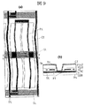
図1(a)は前記画素領域の一実施例の構成を示す平面図である。また、図1(b)は図1(a)のb−b線における断面図、図1(c)は図1(a)のc−c線における断面図、図1(d)は図1(a)のd−d線における断面図である。
【0040】
各図において、透明基板SUB1の液晶側の面に、まず、x方向に延在しy方向に並設される一対のゲート信号線GLが形成されている。
これらゲート信号線GLは後述の一対のドレイン信号線DLとともに矩形状の領域を囲むようになっており、この領域を画素領域として構成するようになっている。
【0041】
そして、この画素領域内における透明基板SUB1の表面には透光性の導電材からなる対向電極CTが該画素領域の周辺の僅かな領域を除く中央部に形成されている。透光性の導電材としては、たとえば、ITO(Indium Tin Oxide)、ITZO(Indium Tin Zinc Oxide)、IZO (Indium Zinc Oxide)、SnO2、In2O3等が用いられる。
【0042】
このようにゲート信号線GLおよび対向電極CTが形成された透明基板SUB1の表面には該ゲート信号線GL等をも被ってたとえばSiNからなる絶縁膜GIが形成されている。
【0043】
この絶縁膜GIは、後述のドレイン信号線DLの形成領域においては前記ゲート信号線GLに対する層間絶縁膜としての機能を、後述の薄膜トランジスタTFTの形成領域においてはそのゲート絶縁膜としての機能を有するようになっている。
【0044】
そして、この絶縁膜GIの表面であって、前記ゲート信号線GLの一部に重畳するようにしてたとえばアモルファスSiからなる半導体層ASが形成されている。
【0045】
この半導体層ASは、薄膜トランジスタTFTのそれであって、その上面にドレイン電極SD1およびソース電極SD2を形成することにより、ゲート信号線の一部をゲート電極とする逆スタガ構造のMIS型トランジスタを構成することができる。
【0046】
ここで、前記ドイレン電極SD1およびソース電極SD2はドレイン信号線DLの形成の際に同時に形成されるようになっている。
【0047】
すなわち、y方向に延在されx方向に並設されるドレイン信号線DLが形成され、その一部が前記半導体層ASの上面にまで延在されてドレイン電極SD1が形成され、また、このドレイン電極SD1と薄膜トランジスタTFTのチャネル長分だけ離間されてソース電極SD2が形成されている。
【0048】
また、このソース電極SD2は画素領域側に若干延在されて後述する画素電極PXとの電気的接続を図るためのコンタクト部COTが形成されている。
【0049】
そして、透明基板SUB1の表面には前記ドレイン信号線DL、ドレイン電極SD1、およびソース電極SD2をも被って保護膜PSV1が形成されている。この保護膜PSV1はたとえばSiN膜等の無機材料層からなり、後述の保護膜PSV2とともに、前記薄膜トランジスタTFTの液晶との直接の接触を回避させるようになっている。該薄膜トランジスタTFTの液晶との接触により特性が変化してしまうのを防止するためである。
【0050】
この保護膜PSV1の表面には、たとえば透光性の導電材で形成される画素電極PXが形成されている。該透光性の導電材として、たとえば、ITO(Indium Tin Oxide)、ITZO(Indium Tin Zinc Oxide)、IZO(Indium Zinc Oxide)、SnO2、In2O3等が用いられる。
【0051】
ここで、この画素電極PXは、図中ほぼx方向に延在しy方向に並設される多数の帯状の電極群から構成されているが、各電極はその延在方向のほぼ中央部に屈曲部を有する山型形状のパターンで形成されている。
【0052】
このような画素電極PXは、特にその辺端部(エッヂ)において前記対向電極CTとの間に電界を生じせしめるようになっているが、上述のパターンとすることにより、いわゆるマルチドメイン方式を採用した構成となっている。
【0053】
すなわち、液晶はその分子配列が同じ状態でも、液晶表示パネルに入射する光の入射方向によって透過光の偏光状態が変化するので、入射方向に対応して光の透過率が異なってしまう。
【0054】
このような液晶表示パネルの視角依存性は視角方向に対し視点を斜めに傾けると、輝度の逆転現象を引き起こすことになり、カラー表示の場合に画像が色づくという表示特性を有する。
【0055】
このため、前記画素電極PXをその延在方向に少なくとも一つの屈曲部を形成したパターンとし、さらにこのパターンを平行にシフトした形状で対向電極CTを形成し、これら各電極の屈曲点を結んだ仮想の線を境にし一方の領域と他方の領域とで各電極間に作用する電界の方向を異ならしめ、これにより、視野角に依存する画像の色づきを補償するようにしている。
【0056】
なお、この実施例では、対向電極CTは画素領域のほぼ全域にわたって形成されたものであるが、そのうち実際に対向電極として機能するのは上述したように画素電極PXを平行にシフトした部分となる。
【0057】
そして、画素電極PXの電極群はそれらが互いに電気的に接続されるために周辺において同一の材料で一体に形成されるようになっている。このことから、画素電極PXは全体として画素領域の周辺の僅かな領域を除く中央部に形成された導電層にそのx方向に延在されy方向に並設された多数スリット(山形状スリット)を形成したパターンとして形成される。
【0058】
また、このようなパターンの画素電極PXの一部は前記保護膜PSV1に予め形成されたスルーホールを通して前記薄膜トランジスタTFTのソース電極SD2のコンタクト部COTに電気的接続がなされるようになっている。
【0059】
さらに、透明基板SUB1の表面には該画素電極PXをも被って保護膜PSV2が形成されている。この保護膜PSV2はたとえば樹脂からなる有機材料からなっている。
【0060】
この保護膜PSV2は、前記保護膜PSV1とともに薄膜トランジスタTFTの液晶の直接の接触を回避する保護膜PSVとして機能することは上述した通りであるが、その材料として有機材料を用いることで表面を平坦化でき、その上方面に形成する配向膜のラビング性を良好にできる。
【0061】
さらに、この保護膜PSV2の表面には前記対向電極CTに信号を供給するための対向電圧信号線CLが形成されている。
この対向電圧信号線CLは電気抵抗の小さい材料が選定され、このことから金属等が用いられている。
【0062】
また、対向電圧信号線CLは、ドレイン信号線DLおよびゲート信号線GLを被うようにした格子状パターンをなし、その開口部は画素領域の周辺の僅かな部分を除いた中央部、すなわち実質的な画素領域を露呈させるように形成されている。
【0063】
このようなパターンで形成された対向電圧信号線CLは、前記液晶表示部ARの周辺のうちいかなる個所、および複数からでも対向電圧信号を供給することができる。このため、対向電圧信号線CLにおける対向電圧信号の波形歪みを無くすことことができ、スメア、輝度傾斜の発生を低減させることができる。
【0064】
また、対向電圧信号線CLの全体として電気抵抗、給電抵抗を小さくできることから、いわゆるコモン反転駆動において、横スメアを1/3以下に低減させることができるようになる。
【0065】
そして、ドレイン信号線DLをその長手方向に沿って被う対向電圧信号線CLはその中心軸をほぼ一致させて該ドレイン信号線DLよりも幅が大きく形成されている。これにより、ドレイン信号線DLからのノイズの原因となる電界を該対向電圧信号線CL側に終端させ、画素電極PXに終端させにくくしている。
【0066】
この場合、ドレイン信号線DLと対向電圧信号線CLとの間の寄生容量は、それらの間に介在される有機材料からなる保護膜PSV2によって大幅に低減されるようになっている。このような保護膜PSV2は誘電率が小さいからである。
【0067】
同様に、ドレイン信号線DLをその長手方向に沿って被う対向電圧信号線CLもその中心軸をほぼ一致させて該ドレイン信号線DLよりも幅が大きく形成されている。
【0068】
この場合、該対向電圧信号線CLは薄膜トランジスタTFTも被うように形成されている。該対向電圧信号線CLは非透光性の金属で形成され、該薄膜トランジスタTFTに照射される外来光を遮光し、該薄膜トランジスタTFTの特性劣化を防止できるからである。
【0069】
なお、該対向電極信号線CLは画素領域内において画素電極PXの一部と重畳する領域を有するようになっており、この領域において、保護膜PSV2を誘電体膜とする容量素子Cstgが形成されている。
【0070】
この容量素子Cstgは、たとえば画素電極PXに供給された映像信号を比較的長く蓄積させる等の機能をもたせるようになっている。
【0071】
そして、このように対向電極CTが形成された透明基板SUB1の上面には該対向電極CTをも被って配向膜(図示せず)が形成されている。この配向膜は液晶と直接に当接する膜で、その表面に形成されたラビングによって該液晶の分子の初期配向方向を決定づけるようになっている。
【0072】
なお、透明基板SUB1と液晶を介して配置される透明基板SUB2の液晶側の面には、カラーフィルタが形成されている。このカラーフィルタはたとえば赤(R)、緑(G)、青(B)の各色のフィルタからなり、y方向に並設される各画素領域群にたとえば赤色のフィルタが共通に形成され、該画素領域群にx方向に順次隣接する画素領域群に共通に赤(R)色、緑(G)色、青(B)色、赤(R)色、……、というような配列で形成されている。
【0073】
そして、カラーフィルタが形成された透明基板の表面にはこれらカラーフィルタをも被って平坦化膜が形成されている。この平坦化膜は塗布によって形成できる樹脂膜からなり、該カラーフィルタの形成によって顕在化する段差をなくすために設けられる。
【0074】
そして、この平坦化膜の表面には配向膜が形成され、この配向膜は液晶と直接に当接する膜で、その表面に形成されたラビングによって該液晶の分子の初期配向方向を決定づけるようになっている。
【0075】
ここで、この実施例では、透明基板SUB2の液晶側の面にはブラックマトリクスが形成されていない構成となっている。透明基板SUB1の液晶側の面に形成された対向電圧信号線CLが該ブラックマトリクスと同様の機能をもつようになるからである。これにより、透明基板SUB1に対する透明基板SUB2の合わせの精度を向上させることができるようになる。
【0076】
実施例2.
図3は、本発明による液晶表示装置の他の実施例を示す構成図で、図1(b)に対応した図となっている。
【0077】
図1(b)の場合と比較して異なる構成は、対向電極CTと対向電圧信号線CLとのスルーホールTHを通しての接続において、画素電極PXを構成する材料層と同一の導電層CNLを介在させていることにある。
【0078】
すなわち、保護膜PSV1の上面に画素電極PXを形成する際に、該保護膜PSV1に形成したスルーホールTH1を通して前記対向電極CTと接続される導電層を同時に形成し、その後、保護膜PSV2の上面に形成された対向電圧信号線CLを該保護膜PSV2に形成したスルーホールTH2を通して前記導電層に接続させることによって構成できる。
【0079】
このようにした場合、対向電極CTと対向電圧信号線CLとの接続部の接触面積の増大を図ることができ、接続を信頼性あるものとすることができる。
【0080】
実施例3.
図4は、本発明による液晶表示装置の他の実施例を示す構成図で、図3に対応した図となっている。
【0081】
図3の場合と比較して異なる構成は、対向電極CTと対向電圧信号線CLとのスルーホールTHを通しての接続において、ドレイン信号線DLを構成する材料層と同一の導電層CNLを介在させていることにある。
【0082】
対向電極CTとして透光性の導電材を用い、また、対向電圧信号線CLとしてたとえばAlあるいはその合金を用いた場合、それらの接続抵抗は大きくなることから、前記ドレイン信号線DLとしてたとえばCr、Mo、W、他の高融点金属あるいはこれらを含む合金等を用い、上述した構成とすることによって、対向電極CTと対向電圧信号線CLとの接続抵抗の低減を図った構成とすることができる。
【0083】
実施例4.
図5は、本発明による液晶表示装置の他の実施例を示す構成図で、図3に対応した図となっている。
【0084】
図3の場合と比較して異なる構成は、保護膜PSV1および絶縁膜GIに形成するスルーホールTH1と絶縁膜PSV2に形成するスルーホールTH2はそれらの中心軸を一致させることなく、それぞれ別な個所に形成することにある。
【0085】
このようにした場合、有機材料からなる保護膜PSV2の表面は、保護膜PSV1および絶縁膜GIのスルーホールTH1の形成個所においても平坦化されるようになる。
【0086】
このことは、保護膜PSV2に形成される凹陥部はスルーホールTH2のみとなるが、その深さは比較的浅いことから、該保護膜PSV2の表面に形成される配向膜のラビング性を向上させることができる。
【0087】
実施例5.
図6は本発明による液晶表示装置の他の実施例を示す構成図で、図1(a)に対応する図となっている。
【0088】
図1(a)の場合と比較して異なる構成は、対向電極CTと対向電圧信号線CLとの接続を図る部分が1個のみならず2個設けられていることにある。
【0089】
上述した構成から明らかなように、対向電極CTと対向電圧信号線CLとの接続は保護膜PSV2、PSV1、および絶縁膜GIの比較的多層である積層体に形成されたスルーホールTHを通して行なわなければならないことから、接続不良の発生を回避するための冗長構成となっている。
【0090】
一方のスルーホールは画素領域を囲む一方のゲート信号線GLに近接させて形成し、他方のスルーホールは他方のゲート信号線GLに近接させて形成している。
【0091】
実施例6.
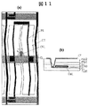
図7(a)は本発明による液晶表示装置の他の実施例を示す平面図で、図1(a)と対応した図となっている。また、図7(b)は図7(a)のb−b線における断面図を示している。
【0092】
図1(a)の場合と比較して異なる構成は画素電極PXにあり、この画素電極PXはy方向にほぼ直線状に延在しx方向に並設された電極群から構成されていることにある。
【0093】
この場合においても、電極群からなる各画素電極PXはその上下端で互いに接続された構成となっている。
【0094】
また、これら画素電極PXをも被って保護膜PSV2が形成され、この保護膜PSV2の上面にドレイン信号線DLおよびゲート信号線GLを被って形成される対向電圧信号線CLが形成されている。
【0095】
このように構成した場合、前記対向電圧信号線CLの開口部の領域内に形成された各画素電極PXのうちドレイン信号線DLに隣接する画素領域は該対向電圧信号線CLにより近接させて配置でき、該対向電圧信号線CLに対向電極CTの機能をもたせてそれらの間に電界を発生せしめるようにできる。
【0096】
このことから、前記対向電圧信号線CLの開口部の領域において無駄な領域を形成することなく、画素領域とすることができ、その開口率を向上させることができる。
【0097】
すなわち、ドレイン信号線DLからの電界はその上部に形成された対向電圧信号線DL側にほぼ集中的に終端され、該対向電圧信号線CLの両側に放射状に拡がってしまう分が減少することになる。このため、該対向電圧信号線CLの近傍においても表示に寄与できる画素領域として構成できるからである。
【0098】
また、上述した構成のようにすることにより、図7(b)に対応する図である図8に示すように、対向電圧信号線CLとそれに隣接する画素電極PXの距離W1を各画素電極PXの間の距離W2に対して異なった値に設定するようにできるようになる。このことは、たとえば画素電極PXの本数が既に定められており、画素領域間の距離を可変するような設定をするような場合において、対向電圧信号線CLとそれに隣接する画素電極PXの前記距離W1を調整することにより、最適な画素構成を容易に実現することができる。
【0099】
さらに、対向電圧信号線CLは誘電率の小さな保護膜PSV2の上面に形成されているため、該対向電圧信号線CLとそれに隣接する画素電極PXとの間の電界強度は、対向電極CTと画素電極PXとの間の電界の強度よりも大きくなる。このため、画素内の輝度均一化を図るためには、W1>W2が望ましく、さらに前記保護膜PSV2の膜厚をdとした場合、W1>W2+dとすることが好ましい。
【0100】
さらに、ドレイン信号線DLからのノイズをより低減させるには、図8に示すようにW1>W3となるように設定することが望ましい。ここで、W3は対向電圧信号線CLに近接して配置される対向電極CTとの離間距離である。このように構成することによって、ドレイン信号線DLからのノイズ電界は、同じ電位である対向電圧信号線CLおよび対向電極CTのなす等電位面に閉じ込められ、外部へのノイズ電界の漏出が抑制されるからである。
【0101】
ここで、対向電圧信号線CLはドレイン信号線DLに対してその走行方向に平行な辺がそれぞれ1/3×W1以上にはみ出して形成することが好ましい。
【0102】
なお、上述した実施例において、各画素電極PXをその長手方向に一つあるいは複数の屈曲部を設けることによってマルチドメイン方式を採用するようにしてもよいことはもちろんである。この場合、これにともない、ドレイン信号線DLおよび対向電圧信号線CLをも画素電極PXをx方向にシフトさせたように屈曲部を有するパターンとすれば、上述した効果を奏することができる。
【0103】
実施例7.
図9(a)は本発明による液晶表示装置の他の実施例を示す平面図で、図7(a)と対応した図となっている。また、図9(b)は図9(a)のb−b線における断面図を示している。
【0104】
図7(a)の場合と比較して異なる構成は、まず、画素電極PXが絶縁膜GI上にてドレイン信号線DLと同層に形成されている。
【0105】
そして、該画素電極PXおよびドレイン信号線DLをも被って保護膜PSV1、保護膜PSV2が順次形成され、該保護膜PSV2の上面にドレイン信号線DLおよびゲート信号線GLをも被って格子状パターンの対向電極CTが形成されている。
【0106】
さらに、この対向電極CTは保護膜PSV2、保護膜PSV1および絶縁膜GIに貫通して形成されたスルーホールTHを通して該絶縁膜GIの下層として形成された対向電圧信号線CLに電気的に接続されている。
【0107】
なお、画素電極PX、対向電極CT(ドレイン信号線DL)はその走行方向に沿って複数の屈曲部が形成されてマルチドメイン方式が採用されている。
【0108】
この場合、対向電圧信号線CLはゲート信号線GLの形成の際に同時に形成され、それらはたとえばAlあるいはその合金層からなるとともに、その表面に陽極化成された酸化膜AOが形成されたものが考えられる。
【0109】
本実施例は、陽極化成された対向電圧信号線CLの一部を露呈させるようにして保護膜PSV2、保護膜PSV1および絶縁膜GIにスルーホールTHを形成し、このスルーホールTHを被うようにして対向電極CTを形成していることにある。
【0110】
すなわち、対向電極CTと対向電圧信号線CLとの電気的接続は前記酸化膜AOを介した容量結合によってなされており、これにより、該接続部における酸化膜AOの除去を特に行なわない構成としている。
【0111】
対向電極CTは格子状のパターンからなることから、この対向電極CTから給電を行なうことができ、対向電圧信号線CLには直接の給電を行なわなくてもいわゆるコモン電位を安定化させる役割りを有する。
【0112】
このことから、他の実施例とし、図10に示すように、陽極化成された対向電圧信号線CLと対向電極CTとの電気的接続部の間にさらにドレイン信号線DLと同一の導電層CNLを介在させるようにしてもよいことはもちろんである。
【0113】
また、このような容量結合の構成を行なった場合、対向電圧信号線CLと対向電極CTとをそれぞれ材料を異にするようにしてもよい。それらの間に応力が発生し結合部でクラックが発生しても直接的な電気的接続が図れるからである。
【0114】
実施例8.
図11(a)は本発明による液晶表示装置の他の実施例を示す平面図で、図9(a)と対応した図となっている。また、図11(b)は図11(a)のb−b線における断面図を示している。
【0115】
図9(a)の場合と比較して、対向電圧信号線CLはAl(あるいはMo、Ti、Ta、W、Zr、Siまたはこれらの一もしくは複数との合金)で構成され、その表面には陽極化成による酸化膜AOが形成されているのは同様であるが、その一部の下層にAlあるいはその合金以外に他の導電層(たとえばCr、Mo、W、Ti、Zrあるいはこれらの一もしくは複数の合金)CNLが形成され、かつ対向電圧信号線CLの形成領域以外の領域にまで延在されて形成されていることにある。
【0116】
この導電層CNLの該延在部は対向電極CTとのコンタクト部として機能するようになっている。前記対向電圧信号線CLを陽極化成しても、前記金属層は陽極化成されることはなく、該対向電圧信号線CLと充分に電気的接続が図れる端子部を形成できるからである。
【0117】
なお、前記導電層CNLは前記延在部を除く部分において対向電圧信号線CLの形成領域の全域に形成されていてもよいことはもちろんである。換言すれば、前記導電層CNLは対向電圧信号線CLと同パターンでしかもその一部において延在部が形成されたパターンとして形成されるようにしてもよい。
【0118】
図12は、本発明による液晶表示装置の他の実施例を示す断面図で、図11(b)に対応した図となっている。
【0119】
前記導電層CNLと対向電極CTとの間にドレイン信号線DLの材料層と同一の導電層CNL2を介して接続を図った構成としたものである。
【0120】
このようにした場合、前記金属層と対向電極CTとの接触面積を増大でき、接続の信頼性を向上させることができる。
【0121】
実施例9.
上記実施例8に示した構成の他の実施例として、前記金属層をITO、IZO等の透光性の導電層に代えて構成してもよい。
【0122】
このようにした場合、対向電極CTも透光性の導電層であることから、それらの接続部においてたとえ面積を増大させても、画素領域の開口率を低減させるようなことにはならないという効果を奏する。
【0123】
実施例10.
図13(a)は、本発明による液晶表示装置の他の実施例を示す断面図で、図11(a)に対応した図となっている。図13(b)は図13(a)のb−b線における断面図である。
【0124】
図11(a)の場合と比較して異なる構成は、対向電極CTと対向電圧信号線CLとの電気接続部において、該対向電圧信号線CLの表面に形成されている酸化膜AOを、その陽極化成時に、部分的に形成されないようにして構成したものである。
【0125】
すなわち、対向電圧信号線CLが形成された透明基板SUB1ごと電界溶液中に浸漬させ、該対向電圧信号線CLを一方の電極、該電界溶液中に浸漬された別個の他の電極板を他方の電極として電圧を印加することにより(陽極化成)、該対向電圧信号線CLの表面に陽極酸化膜を形成させている。
【0126】
この場合、該対向電圧信号線CLの対向電極CTとの接続個所において、レジスト膜を選択的に形成した状態で陽極化成を行なう。この陽極化成が終了した段階で該レジスト膜を除去することで、その部分にAlあるいはその合金の表面が露出した対向電圧信号線CLを得ることができる。
【0127】
なお、前記レジストの形成は、ホトレジストを全面に形成した後、マスク露光により露光し、不要部のレジストを除去する通常の露光処理で行なう。
【0128】
この場合、対向電極CTは、対向電圧信号線CL上の酸化膜AOの除去部のみでなくその周辺の酸化膜AO形成領域上にも形成された構成とすることが望ましい。
【0129】
さもないと、化成されていないAlあるいはその合金が直接絶縁膜GIと相対することになり、いわゆるヒロック発生の懸念があるからである。
【0130】
実施例11.
図14は、本発明による液晶表示装置の他の実施例を示す断面図で、図13(b)に対応した図となっている。
【0131】
図13(b)の場合と比較して異なる構成は、対向電極CTと対向電圧信号線CLとの接続において、絶縁膜GI上に形成されているドレイン信号線DLの材料と同一の導電層CNLを介在させるようにしたことにある。
【0132】
このようにした場合、対向電圧信号線CLのAlあるいはその合金とITO等の透光性の導電層との直接の接続を回避でき、接続抵抗の増大を抑制することができるようになる。透光性の前記導電層は酸化物であるため、Alあるいはその合金と直接に接触させた場合、該Alあるいはその合金が酸化されてしまうため、接続抵抗が増大してしまうからである。
【0133】
実施例12.
図15(a)ないし(c)は本発明による液晶表示装置の他の実施例を示す説明図である。
【0134】
各図は対向電圧信号線CLと対向電極CTとの接続を、たとえば図15(a)では各画素ごとに、図15(b)では隣接する複数の画素においてその一つの画素ごとに、図15(c)ではカラー表示用の3画素においてその一つの画素ごとに設けていることにある。
【0135】
上述したように、対向電圧信号線CLあるいは対向電極CTは各画素領域を画するようにした格子状のパターンとなっていることから、それらの接続においては場所的にも数的にも任意なものとして設定することができる。
【0136】
しかし、対向電圧信号線CLと対向電極CTとの接続を輝度の比較的高い画素内に位置づけることにより、該輝度への影響を防止することができる。
【0137】
また、透明基板SUB1と透明基板SUB2との間にいずれかの基板に形成したいわゆる支柱状のスペーサを設ける場合において、該スペーサを形成する画素領域と、対向電圧信号線CLと対向電極CTとの接続を図る画素領域とを別個にするようにしてもよい。
【0138】
この場合、特定が素領域の立体構造が他の画素に比べ相対的に複雑になることを抑制でき、立体構造の差による予期せぬ不良が特定画素にのみ発生するような憂いを予め回避できる。
【0139】
【発明の効果】
以上説明したことから明らかなように、本発明による液晶表示装置によれば、画素領域の開口率を向上させることができる。また、対向電極と対向電圧信号線の信頼性ある接続を図ることができる。
【図面の簡単な説明】
【図1】本発明による液晶表示装置の画素の一実施例を示す構成図である。
【図2】本発明による液晶表示装置の一実施例を示す構成図である。
【図3】本発明による液晶表示装置の画素の他の実施例を示す断面図である。
【図4】本発明による液晶表示装置の画素の他の実施例を示す断面図である。
【図5】本発明による液晶表示装置の画素の他の実施例を示す断面図である。
【図6】本発明による液晶表示装置の画素の他の実施例を示す平面図である。
【図7】本発明による液晶表示装置の画素の他の実施例を示す構成図である。
【図8】本発明による液晶表示装置の画素の他の実施例を示す断面図である。
【図9】本発明による液晶表示装置の画素の他の実施例を示す構成図である。
【図10】本発明による液晶表示装置の画素の他の実施例を示す断面図である。
【図11】本発明による液晶表示装置の画素の他の実施例を示す構成図である。
【図12】本発明による液晶表示装置の画素の他の実施例を示す断面図である。
【図13】本発明による液晶表示装置の画素の他の実施例を示す構成図である。
【図14】本発明による液晶表示装置の画素の他の実施例を示す断面図である。
【図15】本発明による液晶表示装置の画素の他の実施例を示す説明図である。
【符号の説明】
SUB1…透明基板、GL…ゲート信号線、DL…ドレイン信号線、CL…対向電圧信号線、TFT…薄膜トランジスタ、Cstg…容量素子、PX…画素電極、CT…対向電極、CNL…導電層、GI…絶縁膜(ゲート絶縁膜)、PSV1…保護膜(無機材料)、PSV2…保護膜(有機材料)。[0001]
BACKGROUND OF THE INVENTION
The present invention relates to a liquid crystal display device, and more particularly to a liquid crystal display device called a lateral electric field method.
[0002]
[Prior art]
A liquid crystal display device called a horizontal electric field method is a counter electrode that generates an electric field between a pixel electrode and a pixel electrode in a pixel region on a liquid crystal side surface of one substrate of each substrate that is disposed to face the liquid crystal. The liquid crystal is made to behave by a component substantially parallel to the substrate in the electric field.
[0003]
In the case where such a configuration is applied to an active matrix type, first, a plurality of gate signal lines arranged in parallel on the liquid crystal side surface of the one substrate cross each of these gate signal lines. Each region surrounded by the plurality of drain signal lines arranged in parallel is used as the pixel region.
[0004]
Then, in each of these pixel regions, a thin film transistor operated by a scanning signal from a gate signal line, the pixel electrode to which a video signal from a drain signal line is supplied via the thin film transistor, and a reference to the video signal The counter electrode to which a signal is supplied is provided.
[0005]
Here, the pixel electrode and the counter electrode are each formed as a strip-like pattern extending in one direction, and these electrodes are usually formed in two or more and are alternately arranged.
[0006]
Further, in such a configuration, the counter electrode is formed on the upper surface of the insulating film formed so as to cover the drain signal line, and the central axis of the drain signal line is substantially coincident with the width of the drain signal line. A structure having a large width and formed along the drain signal line is also known.
[0007]
This is because electric lines of force from the drain signal line are easily terminated at the counter electrode above the drain signal line and are prevented from terminating at the pixel electrode. This is because if the electric lines of force terminate in the pixel electrode, it becomes noise.
[0008]
[Problems to be solved by the invention]
However, the liquid crystal display device having such a configuration requires a counter voltage signal line for supplying a signal to the counter electrode, which improves the so-called aperture ratio of the pixel region because it travels and is arranged in the pixel region. There was an inconvenience that it was a hindrance.
[0009]
Further, since the counter electrode and the counter voltage signal line are often arranged through an insulating layer, and their electrical connection is made through a small through hole formed in the insulating layer, further reliability of the connection is desired. It was. This is accompanied by the trend toward higher definition in recent years.
[0010]
The present invention has been made based on such circumstances, and an object thereof is to provide a liquid crystal display device in which the aperture ratio of the pixel region is improved.
[0011]
Another object of the present invention is to provide a liquid crystal display device in which a counter electrode and a counter voltage signal line are reliably connected.
[0012]
[Means for Solving the Problems]
Of the inventions disclosed in this application, the outline of typical ones will be briefly described as follows.
The liquid crystal display device according to the present invention includes, for example, a plurality of gate signal lines arranged side by side on the liquid crystal side surface of one of the substrates that are opposed to each other through the liquid crystal, and intersecting these gate signal lines. A region surrounded by a plurality of drain signal lines arranged in parallel is a pixel region,
In each of these pixel regions, a switching element operated by a scanning signal from a gate signal line, a pixel electrode to which a video signal from a drain signal line is supplied via this switching element, and the above-described voltage via a counter voltage signal line A counter electrode to which a reference signal is supplied with respect to the video signal is formed,
The counter electrode is formed in a lower layer of a laminate of a plurality of insulating layers,
The counter voltage signal line is made of a non-translucent conductor, and is formed in an upper layer of the stacked body of the plurality of insulating layers, forming a lattice pattern covering the gate signal line and the drain signal line, A part thereof is electrically connected to the counter electrode through a through hole formed in the laminate of the plurality of insulating layers.
[0013]
Mean 2.
In the liquid crystal display device according to the present invention, for example, on the premise of the configuration of the
[0014]
Means 3.
In the liquid crystal display device according to the present invention, for example, on the premise of the configuration of the
[0015]
Means 4.
In the liquid crystal display device according to the present invention, for example, on the premise of any one of
[0016]
Means 5.
The liquid crystal display device according to the present invention includes, for example, a plurality of gate signal lines arranged side by side on the liquid crystal side surface of one of the substrates that are opposed to each other through the liquid crystal, and intersecting these gate signal lines. A region surrounded by a plurality of drain signal lines arranged in parallel is a pixel region,
In each of these pixel regions, a switching element operated by a scanning signal from a gate signal line, a pixel electrode to which a video signal from a drain signal line is supplied via this switching element, and the above-described voltage via a counter voltage signal line A counter electrode to which a reference signal is supplied with respect to the video signal is formed,
The counter electrode is formed in a lower layer of a stack of a plurality of insulating layers, and the pixel electrode is formed between two insulating layers of the plurality of insulating layers of the stack in the extending direction of the drain signal line. A plurality of electrode groups extending along the direction intersecting the direction,
The counter voltage signal line is made of a non-translucent conductor, and is formed in an upper layer of the stacked body of the plurality of insulating layers, forming a lattice pattern covering the gate signal line and the drain signal line, A part thereof is electrically connected to the counter electrode through a through hole formed in the laminate of the plurality of insulating layers.
[0017]
Means 6.
The liquid crystal display device according to the present invention, for example, is arranged adjacent to the counter voltage signal line formed by covering the drain signal line when the pixel region is viewed in plan on the premise of the configuration of the means 5. The distance between the pixel electrodes is set larger than the distance between the pixel electrodes arranged adjacent to each other.
[0018]
Mean 7
The liquid crystal display device according to the present invention includes, for example, the counter voltage signal line formed by covering the drain signal line when the pixel region is viewed in plan on the premise of the configuration of any one of the means 5 and 6. The distance between the pixel electrode arranged adjacent to the pixel electrode is set larger than the distance between the counter voltage signal line and the counter electrode arranged adjacent to the counter voltage signal line. is there.
[0019]
Means 8.
The liquid crystal display device according to the present invention includes, for example, a plurality of gate signal lines arranged side by side on the liquid crystal side surface of one of the substrates that are opposed to each other through the liquid crystal, and intersecting these gate signal lines. A region surrounded by a plurality of drain signal lines arranged in parallel is a pixel region,
In each of these pixel regions, a switching element operated by a scanning signal from a gate signal line, a pixel electrode to which a video signal from a drain signal line is supplied via this switching element, and the above-described voltage via a counter voltage signal line A counter electrode to which a reference signal is supplied with respect to the video signal is formed,
The counter voltage signal line is composed of anodized Al or an alloy thereof and is formed in a lower layer of a laminate of a plurality of insulating layers,
The counter electrode is made of a light-transmitting conductor, and is formed in an upper layer of the stacked body of the plurality of insulating layers, and covers the gate signal line and the drain signal line to form a lattice pattern, and a part thereof The capacitor is capacitively coupled to the counter voltage signal line through through holes formed in the laminate of the plurality of insulating layers.
[0020]
Means 9.
The liquid crystal display device according to the present invention includes, for example, a plurality of gate signal lines arranged side by side on the liquid crystal side surface of one of the substrates that are opposed to each other through the liquid crystal, and intersecting these gate signal lines. A region surrounded by a plurality of drain signal lines arranged in parallel is a pixel region,
In each of these pixel regions, a switching element operated by a scanning signal from a gate signal line, a pixel electrode to which a video signal from a drain signal line is supplied via this switching element, and the above-described voltage via a counter voltage signal line A counter electrode to which a reference signal is supplied with respect to the video signal is formed,
The counter voltage signal line is composed of anodized Al or an alloy thereof and is formed in a lower layer of a laminate of a plurality of insulating layers, and the counter voltage signal line is formed in at least a part of the lower layer of the counter voltage signal line. A conductive material layer exposed from the counter voltage signal line;
The counter electrode is formed in an upper layer of the stacked body of the plurality of insulating layers, covers the gate signal line and the drain signal line to form a lattice pattern, and a stacked body of the plurality of insulating layers in a part thereof It is electrically connected to the conductive material layer through a through-hole formed in.
[0021]
Means 10.
The liquid crystal display device according to the present invention is characterized in that, for example, on the premise of the configuration of the means 9, the counter electrode is composed of a translucent conductive layer.
[0022]
In the liquid crystal display device according to the present invention, for example, a drain signal line is formed between two insulating layers of the laminate of a plurality of insulating layers on the premise of any one of the means 9 and 10, and the counter electrode The same material layer as that of the drain signal line is interposed between the conductive material layer and the conductive material layer.
[0023]
In addition, this invention is not limited to the above structure, A various change is possible in the range which does not deviate from the technical idea of this invention.
[0024]
DETAILED DESCRIPTION OF THE INVENTION
Hereinafter, embodiments of a liquid crystal display device according to the present invention will be described with reference to the drawings.
Example 1.
"overall structure"
FIG. 2 is an overall configuration diagram showing an embodiment of a liquid crystal display device according to the present invention. Although this figure is an equivalent circuit diagram, it is drawn in correspondence with the actual geometric arrangement.
[0025]
In the figure, there is a pair of transparent substrates SUB1 and SUB2 arranged to face each other via a liquid crystal, and the liquid crystal is sealed by a sealing material SL that also serves to fix the other transparent substrate SUB2 to one transparent substrate SUB1.
[0026]
On the liquid crystal side surface of the one transparent substrate SUB1 surrounded by the sealing material SL, the gate signal lines GL extending in the x direction and arranged in parallel in the y direction, and extending in the y direction and aligned in the x direction. A drain signal line DL is provided.
[0027]
A region surrounded by each gate signal line GL and each drain signal line DL constitutes a pixel region, and a matrix aggregate of these pixel regions constitutes a liquid crystal display unit AR.
[0028]
A common counter voltage signal line CL that runs in each pixel region is formed in each pixel region arranged in parallel in the x direction. The counter voltage signal line CL serves as a signal line for supplying a reference voltage for a video signal to a counter electrode CT (described later) in each pixel region.
[0029]
In each pixel region, a thin film transistor TFT operated by a scanning signal from one side gate signal line GL and a pixel electrode PX to which a video signal from one side drain signal line DL is supplied via the thin film transistor TFT are formed. Has been.
[0030]
The pixel electrode PX generates an electric field with the counter electrode CT connected to the counter voltage signal line CL, and the light transmittance of the liquid crystal is controlled by the electric field.
[0031]
One end of each of the gate signal lines GL extends beyond the sealing material SL, and the extending end constitutes a terminal to which the output terminal of the vertical scanning drive circuit V is connected. The input terminal of the vertical scanning drive circuit V receives a signal from a printed circuit board disposed outside the liquid crystal display panel.
[0032]
The vertical scanning drive circuit V is composed of a plurality of semiconductor devices, and a plurality of adjacent gate signal lines GL are grouped, and one semiconductor device is assigned to each group.
[0033]
Similarly, one end of each of the drain signal lines DL extends beyond the seal material SL, and the extending end constitutes a terminal to which the output terminal of the video signal driving circuit He is connected. . The input terminal of the video signal driving circuit He is adapted to receive a signal from a printed circuit board arranged outside the liquid crystal display panel.
[0034]
The video signal drive circuit He is also composed of a plurality of semiconductor devices, and a plurality of adjacent drain signal lines DL are grouped, and one semiconductor device is assigned to each group. .
[0035]
The counter voltage signal lines CL are connected in common at the end on the right side in the figure, and the connection line extends beyond the seal material SL, and constitutes a terminal CLT at the extended end. A voltage serving as a reference for the video signal is supplied from the terminal CLT.
[0036]
One of the gate signal lines GL is sequentially selected by a scanning signal from the vertical scanning circuit V.
[0037]
In addition, a video signal is supplied to each of the drain signal lines DL by the video signal driving circuit He in accordance with the selection timing of the gate signal line GL.
[0038]
In the above-described embodiment, the vertical scanning drive circuit V and the video signal drive circuit He indicate the semiconductor device mounted on the transparent substrate SUB1, but for example, straddle between the transparent substrate SUB1 and the printed circuit board. It may be a so-called tape carrier type semiconductor device to be connected. Further, when the semiconductor layer of the thin film transistor TFT is made of polycrystalline silicon (p-Si), the transparent substrate SUB1 is made of the polycrystalline silicon. A semiconductor element may be formed together with a wiring layer.
[0039]
<Pixel configuration>
FIG. 1A is a plan view showing a configuration of an embodiment of the pixel region. 1B is a cross-sectional view taken along line bb in FIG. 1A, FIG. 1C is a cross-sectional view taken along line cc in FIG. 1A, and FIG. It is sectional drawing in the dd line | wire of (a).
[0040]
In each drawing, a pair of gate signal lines GL extending in the x direction and arranged in parallel in the y direction are first formed on the liquid crystal side surface of the transparent substrate SUB1.
These gate signal lines GL surround a rectangular region together with a pair of drain signal lines DL described later, and this region is configured as a pixel region.
[0041]
A counter electrode CT made of a translucent conductive material is formed on the surface of the transparent substrate SUB1 in the pixel region at the center except for a slight region around the pixel region. Examples of the light-transmitting conductive material include ITO (Indium Tin Oxide), ITZO (Indium Tin Zinc Oxide), IZO (Indium Zinc Oxide), and SnO. 2 , In 2 O 3 Etc. are used.
[0042]
Thus, on the surface of the transparent substrate SUB1 on which the gate signal line GL and the counter electrode CT are formed, an insulating film GI made of, for example, SiN is formed so as to cover the gate signal line GL and the like.
[0043]
This insulating film GI functions as an interlayer insulating film for the gate signal line GL in a region where a drain signal line DL described later is formed, and functions as a gate insulating film in a region where a thin film transistor TFT described later is formed. It has become.
[0044]
A semiconductor layer AS made of, for example, amorphous Si is formed on the surface of the insulating film GI so as to overlap a part of the gate signal line GL.
[0045]
This semiconductor layer AS is that of the thin film transistor TFT, and by forming the drain electrode SD1 and the source electrode SD2 on the upper surface thereof, an MIS type transistor having an inverted stagger structure having a part of the gate signal line as the gate electrode is formed. be able to.
[0046]
Here, the drain electrode SD1 and the source electrode SD2 are formed simultaneously with the formation of the drain signal line DL.
[0047]
That is, a drain signal line DL extending in the y direction and arranged in parallel in the x direction is formed, and a part of the drain signal line DL extends to the upper surface of the semiconductor layer AS to form the drain electrode SD1. A source electrode SD2 is formed so as to be separated from the electrode SD1 by the channel length of the thin film transistor TFT.
[0048]
Further, the source electrode SD2 is slightly extended to the pixel region side to form a contact portion COT for electrical connection with a pixel electrode PX described later.
[0049]
A protective film PSV1 is formed on the surface of the transparent substrate SUB1 so as to cover the drain signal line DL, the drain electrode SD1, and the source electrode SD2. This protective film PSV1 is made of an inorganic material layer such as a SiN film, for example, and avoids direct contact with the liquid crystal of the thin film transistor TFT together with the protective film PSV2 described later. This is to prevent the characteristics from changing due to the contact of the thin film transistor TFT with the liquid crystal.
[0050]
On the surface of the protective film PSV1, pixel electrodes PX made of, for example, a translucent conductive material are formed. Examples of the light-transmitting conductive material include ITO (Indium Tin Oxide), ITZO (Indium Tin Zinc Oxide), IZO (Indium Zinc Oxide), and SnO. 2 , In 2 O 3 Etc. are used.
[0051]
Here, the pixel electrode PX is composed of a number of strip-shaped electrode groups extending in the x direction and arranged in parallel in the y direction in the figure, but each electrode is in a substantially central portion in the extending direction. It is formed with a mountain-shaped pattern having a bent portion.
[0052]
Such a pixel electrode PX generates an electric field between the pixel electrode PX and the counter electrode CT, particularly at its edge (edge). By adopting the above-mentioned pattern, a so-called multi-domain method is adopted. It has become the composition.
[0053]
In other words, even when the molecular arrangement of the liquid crystal is the same, the polarization state of the transmitted light changes depending on the incident direction of the light incident on the liquid crystal display panel, so that the light transmittance varies depending on the incident direction.
[0054]
The viewing angle dependency of such a liquid crystal display panel has a display characteristic that when the viewpoint is tilted with respect to the viewing angle direction, a luminance reversal phenomenon is caused, and an image is colored in the case of color display.
[0055]
Therefore, the pixel electrode PX has a pattern in which at least one bent portion is formed in the extending direction, and the counter electrode CT is formed in a shape in which this pattern is shifted in parallel, and the bent points of these electrodes are connected. The direction of the electric field acting between the electrodes is made different between one region and the other region with the virtual line as a boundary, thereby compensating for the coloring of the image depending on the viewing angle.
[0056]
In this embodiment, the counter electrode CT is formed over almost the entire pixel region, but the portion that actually functions as the counter electrode is a portion obtained by shifting the pixel electrode PX in parallel as described above. .
[0057]
The electrode groups of the pixel electrodes PX are integrally formed of the same material in the periphery so that they are electrically connected to each other. Therefore, the pixel electrode PX as a whole is a multiplicity of slits (mountain-shaped slits) extending in the x direction and juxtaposed in the y direction on a conductive layer formed in the central portion excluding a small area around the pixel area. Is formed as a pattern.
[0058]
A part of the pixel electrode PX having such a pattern is electrically connected to the contact portion COT of the source electrode SD2 of the thin film transistor TFT through a through hole previously formed in the protective film PSV1.
[0059]
Further, a protective film PSV2 is formed on the surface of the transparent substrate SUB1 so as to cover the pixel electrode PX. This protective film PSV2 is made of an organic material made of resin, for example.
[0060]
As described above, this protective film PSV2 functions as a protective film PSV that avoids direct contact with the liquid crystal of the thin film transistor TFT together with the protective film PSV1, but the surface is flattened by using an organic material as the material. In addition, the rubbing property of the alignment film formed on the upper surface can be improved.
[0061]
Further, a counter voltage signal line CL for supplying a signal to the counter electrode CT is formed on the surface of the protective film PSV2.
For the counter voltage signal line CL, a material having a small electric resistance is selected, and therefore metal or the like is used.
[0062]
Further, the counter voltage signal line CL has a lattice pattern that covers the drain signal line DL and the gate signal line GL, and the opening is a central portion excluding a slight portion around the pixel region, that is, substantially It is formed so that a typical pixel region is exposed.
[0063]
The counter voltage signal line CL formed in such a pattern can supply a counter voltage signal from any location and a plurality of locations around the liquid crystal display AR. For this reason, the waveform distortion of the counter voltage signal in the counter voltage signal line CL can be eliminated, and the occurrence of smear and luminance gradient can be reduced.
[0064]
Further, since the electrical resistance and the feeding resistance can be reduced as a whole of the counter voltage signal line CL, the lateral smear can be reduced to 1/3 or less in so-called common inversion driving. In Become.
[0065]
The counter voltage signal line CL that covers the drain signal line DL along the longitudinal direction thereof is formed to have a width larger than that of the drain signal line DL so that the central axes thereof are substantially aligned. Thus, the electric field that causes noise from the drain signal line DL is terminated on the counter voltage signal line CL side, and is difficult to terminate on the pixel electrode PX.
[0066]
In this case, the parasitic capacitance between the drain signal line DL and the counter voltage signal line CL is greatly reduced by the protective film PSV2 made of an organic material interposed therebetween. This is because such a protective film PSV2 has a small dielectric constant.
[0067]
Similarly, the counter voltage signal line CL covering the drain signal line DL along the longitudinal direction thereof is formed to have a width larger than that of the drain signal line DL so that the central axes thereof are substantially aligned.
[0068]
In this case, the counter voltage signal line CL is formed to cover the thin film transistor TFT. This is because the counter voltage signal line CL is formed of a non-translucent metal and can shield extraneous light applied to the thin film transistor TFT, thereby preventing characteristic deterioration of the thin film transistor TFT.
[0069]
The counter electrode signal line CL has a region overlapping with a part of the pixel electrode PX in the pixel region. In this region, the capacitor element Cstg having the protective film PSV2 as a dielectric film is formed. ing.
[0070]
The capacitive element Cstg has a function of, for example, accumulating a video signal supplied to the pixel electrode PX for a relatively long time.
[0071]
An alignment film (not shown) is formed on the upper surface of the transparent substrate SUB1 on which the counter electrode CT is formed in such a manner so as to cover the counter electrode CT. This alignment film is in direct contact with the liquid crystal, and the initial alignment direction of the molecules of the liquid crystal is determined by rubbing formed on the surface thereof.
[0072]
A color filter is formed on the liquid crystal side surface of the transparent substrate SUB1 and the transparent substrate SUB2 disposed via the liquid crystal. This color filter is made up of, for example, red (R), green (G), and blue (B) filters. For example, a red filter is commonly formed in each pixel region group arranged in the y direction. It is formed in an arrangement such as red (R) color, green (G) color, blue (B) color, red (R) color,... Common to pixel region groups that are sequentially adjacent to the region group in the x direction. Yes.
[0073]
A flattening film is formed on the surface of the transparent substrate on which the color filters are formed so as to cover these color filters. This flattening film is made of a resin film that can be formed by coating, and is provided to eliminate a step that becomes obvious due to the formation of the color filter.
[0074]
An alignment film is formed on the surface of the flattening film, and the alignment film is a film in direct contact with the liquid crystal, and the initial alignment direction of the molecules of the liquid crystal is determined by rubbing formed on the surface. ing.
[0075]
In this embodiment, the black matrix is not formed on the liquid crystal side surface of the transparent substrate SUB2. This is because the counter voltage signal line CL formed on the surface of the transparent substrate SUB1 on the liquid crystal side has the same function as the black matrix. Thereby, the precision of alignment of the transparent substrate SUB2 with respect to the transparent substrate SUB1 can be improved.
[0076]
Example 2
FIG. 3 is a block diagram showing another embodiment of the liquid crystal display device according to the present invention and corresponds to FIG.
[0077]
1B is different from the case of FIG. 1B in that the counter electrode CT and the counter voltage signal line CL are connected through the through hole TH, and the same conductive layer CNL as the material layer forming the pixel electrode PX is interposed. It is in letting it be.
[0078]
That is, when the pixel electrode PX is formed on the upper surface of the protective film PSV1, a conductive layer connected to the counter electrode CT is simultaneously formed through the through hole TH1 formed in the protective film PSV1, and then the upper surface of the protective film PSV2 is formed. The counter voltage signal line CL formed in (1) is connected to the conductive layer through a through hole TH2 formed in the protective film PSV2.
[0079]
In this case, the contact area of the connection portion between the counter electrode CT and the counter voltage signal line CL can be increased, and the connection can be made reliable.
[0080]
Example 3
FIG. 4 is a block diagram showing another embodiment of the liquid crystal display device according to the present invention and corresponds to FIG.
[0081]
3 differs from the case of FIG. 3 in that the conductive layer CNL, which is the same as the material layer constituting the drain signal line DL, is interposed in the connection between the counter electrode CT and the counter voltage signal line CL through the through hole TH. There is to be.
[0082]
When a translucent conductive material is used as the counter electrode CT and, for example, Al or an alloy thereof is used as the counter voltage signal line CL, their connection resistance increases. Therefore, as the drain signal line DL, for example, Cr, By using Mo, W, another refractory metal, an alloy containing these, or the like, and having the above-described configuration, it is possible to reduce the connection resistance between the counter electrode CT and the counter voltage signal line CL. .
[0083]
Example 4
FIG. 5 is a block diagram showing another embodiment of the liquid crystal display device according to the present invention and corresponds to FIG.
[0084]
3 differs from the case of FIG. 3 in that the through hole TH1 formed in the protective film PSV1 and the insulating film GI and the through hole TH2 formed in the insulating film PSV2 are different from each other without matching their central axes. There is in forming.
[0085]
In such a case, the surface of the protective film PSV2 made of an organic material is flattened even at the positions where the protective film PSV1 and the through hole TH1 of the insulating film GI are formed.
[0086]
This is because the concave portion formed in the protective film PSV2 is only the through hole TH2, but the depth is relatively shallow, so that the rubbing property of the alignment film formed on the surface of the protective film PSV2 is improved. be able to.
[0087]
Example 5 FIG.
FIG. 6 is a block diagram showing another embodiment of the liquid crystal display device according to the present invention and corresponds to FIG.
[0088]
A configuration different from the case of FIG. 1A is that not only one part but also two parts are provided to connect the counter electrode CT and the counter voltage signal line CL.
[0089]
As is clear from the above-described configuration, the connection between the counter electrode CT and the counter voltage signal line CL must be made through a through hole TH formed in a laminate having a relatively multilayer structure of the protective films PSV2, PSV1, and the insulating film GI. Therefore, a redundant configuration is provided to avoid the occurrence of connection failure.
[0090]
One through hole is formed close to one gate signal line GL surrounding the pixel region, and the other through hole is formed close to the other gate signal line GL.
[0091]
Example 6
FIG. 7A is a plan view showing another embodiment of the liquid crystal display device according to the present invention and corresponds to FIG. Moreover, FIG.7 (b) has shown sectional drawing in the bb line of Fig.7 (a).
[0092]
The pixel electrode PX has a different configuration compared to the case of FIG. 1A, and the pixel electrode PX is composed of an electrode group extending substantially linearly in the y direction and arranged in parallel in the x direction. It is in.
[0093]
Also in this case, the pixel electrodes PX formed of the electrode group are connected to each other at the upper and lower ends.
[0094]
A protective film PSV2 is formed so as to cover the pixel electrodes PX, and a counter voltage signal line CL formed so as to cover the drain signal line DL and the gate signal line GL is formed on the upper surface of the protective film PSV2.
[0095]
When configured in this manner, the pixel region adjacent to the drain signal line DL among the pixel electrodes PX formed in the region of the opening of the counter voltage signal line CL is disposed closer to the counter voltage signal line CL. In addition, the counter voltage signal line CL can have the function of the counter electrode CT to generate an electric field therebetween.
[0096]
Therefore, a pixel region can be formed without forming a useless region in the region of the opening of the counter voltage signal line CL, and the aperture ratio can be improved.
[0097]
That is, the electric field from the drain signal line DL is terminated almost intensively on the side of the counter voltage signal line DL formed on the upper side, and the amount of radial expansion on both sides of the counter voltage signal line CL is reduced. Become. For this reason, it can be configured as a pixel region that can contribute to display even in the vicinity of the counter voltage signal line CL.
[0098]
Further, by adopting the above-described configuration, as shown in FIG. 8 corresponding to FIG. 7B, the distance W1 between the counter voltage signal line CL and the pixel electrode PX adjacent thereto is set to each pixel electrode PX. It becomes possible to set different values for the distance W2. This is because, for example, when the number of pixel electrodes PX is already determined and the distance between the pixel regions is set to be variable, the distance between the counter voltage signal line CL and the pixel electrode PX adjacent thereto is set. By adjusting W1, an optimal pixel configuration can be easily realized.
[0099]
Further, since the counter voltage signal line CL is formed on the upper surface of the protective film PSV2 having a small dielectric constant, the electric field strength between the counter voltage signal line CL and the pixel electrode PX adjacent thereto is equal to the counter electrode CT and the pixel. It becomes larger than the intensity of the electric field between the electrodes PX. For this reason, W1> W2 is desirable in order to make the luminance uniform in the pixel, and when the film thickness of the protective film PSV2 is d, it is preferable to satisfy W1> W2 + d.
[0100]
Further, in order to further reduce the noise from the drain signal line DL, it is desirable to set W1> W3 as shown in FIG. Here, W3 is a separation distance from the counter electrode CT arranged close to the counter voltage signal line CL. With this configuration, the noise electric field from the drain signal line DL is confined to the equipotential surface formed by the counter voltage signal line CL and the counter electrode CT having the same potential, and leakage of the noise electric field to the outside is suppressed. This is because that.
[0101]
Here, the counter voltage signal line CL is preferably formed so that the sides parallel to the running direction with respect to the drain signal line DL protrude beyond 1/3 × W1.
[0102]
In the above-described embodiment, it is needless to say that the multi-domain method may be adopted by providing each pixel electrode PX with one or a plurality of bent portions in the longitudinal direction. In this case, if the drain signal line DL and the counter voltage signal line CL are also formed into a pattern having a bent portion such that the pixel electrode PX is shifted in the x direction, the above-described effects can be obtained.
[0103]
Example 7
FIG. 9A is a plan view showing another embodiment of the liquid crystal display device according to the present invention and corresponds to FIG. 7A. FIG. 9B is a cross-sectional view taken along the line bb in FIG. 9A.
[0104]
In the configuration different from that in FIG. 7A, first, the pixel electrode PX is formed in the same layer as the drain signal line DL on the insulating film GI.
[0105]
Then, the protective film PSV1 and the protective film PSV2 are sequentially formed so as to cover the pixel electrode PX and the drain signal line DL, and the drain signal line DL and the gate signal line GL are also covered on the upper surface of the protective film PSV2. Counter electrode CT is formed.
[0106]
Further, the counter electrode CT is electrically connected to a counter voltage signal line CL formed as a lower layer of the insulating film GI through a through hole TH formed through the protective film PSV2, the protective film PSV1, and the insulating film GI. ing.
[0107]
Note that the pixel electrode PX and the counter electrode CT (drain signal line DL) are formed with a plurality of bent portions along the traveling direction, and a multi-domain method is adopted.
[0108]
In this case, the counter voltage signal line CL is formed at the same time when the gate signal line GL is formed. The counter voltage signal line CL is made of, for example, Al or an alloy layer thereof, and an anodized oxide film AO is formed on the surface thereof. Conceivable.
[0109]
In this embodiment, a through hole TH is formed in the protective film PSV2, the protective film PSV1, and the insulating film GI so as to expose a part of the anodized counter voltage signal line CL, and this through hole TH is covered. Thus, the counter electrode CT is formed.
[0110]
That is, the electrical connection between the counter electrode CT and the counter voltage signal line CL is made by capacitive coupling through the oxide film AO, whereby the oxide film AO is not particularly removed from the connection portion. .
[0111]
Since the counter electrode CT has a grid pattern, power can be supplied from the counter electrode CT, and the counter voltage signal line CL has a role of stabilizing a so-called common potential without direct power supply. Have.
[0112]
Therefore, in another embodiment, as shown in FIG. 10, the same conductive layer CNL as the drain signal line DL is further provided between the anodized counter voltage signal line CL and the counter electrode CT. Of course, it may be made to intervene.
[0113]
When such a capacitive coupling configuration is performed, the counter voltage signal line CL and the counter electrode CT may be made of different materials. This is because a direct electrical connection can be achieved even if a stress is generated between them and a crack occurs at the joint.
[0114]
Example 8 FIG.
FIG. 11A is a plan view showing another embodiment of the liquid crystal display device according to the present invention and corresponds to FIG. 9A. Moreover, FIG.11 (b) has shown sectional drawing in the bb line of Fig.11 (a).
[0115]
Compared to the case of FIG. 9A, the counter voltage signal line CL is made of Al (or Mo, Ti, Ta, W, Zr, Si, or an alloy of one or more of these), and on the surface thereof It is the same that the oxide film AO is formed by anodization, but a part of the lower layer other than Al or its alloy To others The conductive layer (for example, Cr, Mo, W, Ti, Zr or one or a plurality of alloys thereof) CNL is formed and extended to a region other than the region where the counter voltage signal line CL is formed. There is.
[0116]
The extending portion of the conductive layer CNL functions as a contact portion with the counter electrode CT. This is because even if the counter voltage signal line CL is anodized, the metal layer is not anodized, and a terminal portion that can be sufficiently electrically connected to the counter voltage signal line CL can be formed.
[0117]
Needless to say, the conductive layer CNL may be formed in the entire region where the counter voltage signal line CL is formed, except for the extended portion. In other words, the conductive layer CNL may be formed as a pattern having the same pattern as the counter voltage signal line CL and a part of which is extended.
[0118]
FIG. 12 is a sectional view showing another embodiment of the liquid crystal display device according to the present invention and corresponds to FIG.
[0119]
The conductive layer CNL and the counter electrode CT are connected via the same conductive layer CNL2 as the material layer of the drain signal line DL.
[0120]
In this case, the contact area between the metal layer and the counter electrode CT can be increased, and the connection reliability can be improved.
[0121]
Example 9
As another example of the configuration shown in Example 8, the metal layer may be replaced with a light-transmitting conductive layer such as ITO or IZO.
[0122]
In this case, since the counter electrode CT is also a light-transmitting conductive layer, the aperture ratio of the pixel region is not reduced even if the area is increased in the connection portion. Play.
[0123]
Example 10
FIG. 13A is a sectional view showing another embodiment of the liquid crystal display device according to the present invention and corresponds to FIG. FIG.13 (b) is sectional drawing in the bb line of Fig.13 (a).
[0124]
11A is different from the case of FIG. 11A in that an oxide film AO formed on the surface of the counter voltage signal line CL is formed at the electrical connection portion between the counter electrode CT and the counter voltage signal line CL. It is configured such that it is not partially formed during anodization.
[0125]
That is, the transparent substrate SUB1 on which the counter voltage signal line CL is formed is immersed in the electric field solution, the counter voltage signal line CL is set as one electrode, and another electrode plate immersed in the electric field solution is set as the other electrode plate. By applying a voltage as an electrode (anodization), an anodic oxide film is formed on the surface of the counter voltage signal line CL.
[0126]
In this case, anodization is performed in a state where the resist film is selectively formed at the connection portion of the counter voltage signal line CL with the counter electrode CT. By removing the resist film at the stage where the anodization is completed, it is possible to obtain the counter voltage signal line CL in which the surface of Al or its alloy is exposed.
[0127]
The resist is formed by a normal exposure process in which a photoresist is formed on the entire surface, then exposed by mask exposure, and unnecessary resist is removed.
[0128]
In this case, it is desirable that the counter electrode CT be formed not only on the oxide film AO removal portion on the counter voltage signal line CL but also on the oxide film AO formation region around it.
[0129]
Otherwise, unformed Al or an alloy thereof is directly opposed to the insulating film GI, and so-called hillock may be generated.
[0130]
Example 11
FIG. 14 is a sectional view showing another embodiment of the liquid crystal display device according to the present invention and corresponds to FIG.
[0131]
The configuration different from the case of FIG. 13B is the same conductive layer CNL as the material of the drain signal line DL formed on the insulating film GI in the connection between the counter electrode CT and the counter voltage signal line CL. This is because of interposing.
[0132]
In this case, direct connection between Al of the counter voltage signal line CL or an alloy thereof and a light-transmitting conductive layer such as ITO can be avoided, and an increase in connection resistance can be suppressed. This is because, since the light-transmitting conductive layer is an oxide, when it is brought into direct contact with Al or an alloy thereof, the Al or the alloy thereof is oxidized, resulting in an increase in connection resistance.
[0133]
Example 12 FIG.
FIGS. 15A to 15C are explanatory views showing another embodiment of the liquid crystal display device according to the present invention.
[0134]
Each figure shows the connection between the counter voltage signal line CL and the counter electrode CT, for example, for each pixel in FIG. 15A, and for each pixel in a plurality of adjacent pixels in FIG. In (c), three pixels for color display are provided for each pixel.
[0135]
As described above, the counter voltage signal line CL or the counter electrode CT has a lattice pattern that defines each pixel region. Therefore, the connection is arbitrary in terms of location and number. Can be set as things.
[0136]
However, by positioning the connection between the counter voltage signal line CL and the counter electrode CT in a pixel having a relatively high luminance, the influence on the luminance can be prevented.
[0137]
In the case where a so-called columnar spacer formed on one of the substrates is provided between the transparent substrate SUB1 and the transparent substrate SUB2, the pixel region in which the spacer is formed, the counter voltage signal line CL, and the counter electrode CT The pixel region to be connected may be separated.
[0138]
In this case, the three-dimensional structure of the elementary region can be suppressed from becoming relatively complicated compared to other pixels, and the anxiety that an unexpected defect due to the difference in the three-dimensional structure occurs only in the specific pixel can be avoided in advance. .
[0139]
【The invention's effect】
As is apparent from the above description, according to the liquid crystal display device of the present invention, the aperture ratio of the pixel region can be improved. In addition, a reliable connection between the counter electrode and the counter voltage signal line can be achieved.
[Brief description of the drawings]
FIG. 1 is a configuration diagram illustrating one embodiment of a pixel of a liquid crystal display device according to the present invention.
FIG. 2 is a block diagram showing an embodiment of a liquid crystal display device according to the present invention.
FIG. 3 is a cross-sectional view showing another embodiment of the pixel of the liquid crystal display device according to the present invention.
FIG. 4 is a cross-sectional view showing another embodiment of the pixel of the liquid crystal display device according to the present invention.
FIG. 5 is a cross-sectional view showing another embodiment of the pixel of the liquid crystal display device according to the present invention.
FIG. 6 is a plan view showing another embodiment of the pixel of the liquid crystal display device according to the present invention.
FIG. 7 is a block diagram showing another embodiment of the pixel of the liquid crystal display device according to the present invention.
FIG. 8 is a cross-sectional view showing another embodiment of the pixel of the liquid crystal display device according to the present invention.
FIG. 9 is a block diagram showing another embodiment of the pixel of the liquid crystal display device according to the present invention.
FIG. 10 is a cross-sectional view showing another embodiment of the pixel of the liquid crystal display device according to the present invention.
FIG. 11 is a block diagram showing another embodiment of the pixel of the liquid crystal display device according to the present invention.
FIG. 12 is a cross-sectional view showing another embodiment of the pixel of the liquid crystal display device according to the present invention.
FIG. 13 is a block diagram showing another embodiment of the pixel of the liquid crystal display device according to the present invention.
FIG. 14 is a cross-sectional view showing another embodiment of the pixel of the liquid crystal display device according to the present invention.
FIG. 15 is an explanatory view showing another embodiment of the pixel of the liquid crystal display device according to the present invention.
[Explanation of symbols]
SUB1 ... transparent substrate, GL ... gate signal line, DL ... drain signal line, CL ... counter voltage signal line, TFT ... thin film transistor, Cstg ... capacitor element, PX ... pixel electrode, CT ... counter electrode, CNL ... conductive layer, GI ... Insulating film (gate insulating film), PSV1 ... protective film (inorganic material), PSV2 ... protective film (organic material).
Claims (9)
これら各画素領域に、ゲート信号線からの走査信号によって作動されるスイッチング素子と、このスイッチング素子を介してドレイン信号線からの映像信号が供給される画素電極と、対向電圧信号線を介して前記映像信号に対して基準となる信号が供給される対向電極とが形成され、
前記対向電極と前記画素電極との間に第1の絶縁層を有し、前記画素電極と前記対向電圧信号線との間に第2の絶縁層を有し、
前記対向電極は、透光性の導電体からなるとともに、前記第1の絶縁層の下層に形成され、
前記対向電圧信号線は、非透光性の導電体からなるとともに、前記第2の絶縁層の上層に形成され、前記ゲート信号線およびドレイン信号線をも被って格子状パターンをなし、
前記画素電極と同層に形成される導電層と、前記導電層と前記対向電極とを電気的に接続し前記第1の絶縁層を貫通して形成される第1のスルーホールと、前記導電層と前記対向電圧信号線とを電気的に接続し前記第2の絶縁層を貫通して形成される第2のスルーホールとを有し、前記第1及び第2のスルーホールは、その中心軸が異なるように形成されることを特徴とする液晶表示装置。A plurality of gate signal lines juxtaposed on the liquid crystal side surface of one of the substrates opposed to each other through the liquid crystal, and a plurality of drain signal lines juxtaposed across the gate signal lines The area surrounded by
In each of these pixel regions, a switching element operated by a scanning signal from a gate signal line, a pixel electrode to which a video signal from a drain signal line is supplied via this switching element, and the above-described voltage via a counter voltage signal line A counter electrode to which a reference signal is supplied with respect to the video signal is formed,
Having a first insulating layer between the counter electrode and the pixel electrode, and having a second insulating layer between the pixel electrode and the counter voltage signal line;
The counter electrode is made of a light-transmitting conductor and is formed under the first insulating layer,
The counter voltage signal line is made of a non-translucent conductor and is formed in an upper layer of the second insulating layer, covering the gate signal line and the drain signal line to form a lattice pattern,
A conductive layer formed on the pixel electrode in the same layer, and the said counter electrode and said conductive layer electrically connected to the first through-hole formed through the first insulating layer, the conductive A second through hole electrically connecting the layer and the counter voltage signal line and penetrating through the second insulating layer , wherein the first and second through holes have their centers A liquid crystal display device, wherein the axes are formed differently.
これら各画素領域に、ゲート信号線からの走査信号によって作動されるスイッチング素子と、このスイッチング素子を介してドレイン信号線からの映像信号が供給される画素電極と、対向電圧信号線を介して前記映像信号に対して基準となる信号が供給される対向電極とが形成され、
前記対向電極と前記画素電極との間に第1の絶縁層を有し、前記画素電極と前記対向電圧信号線との間に第2の絶縁層を有し、
前記対向電極は、透光性の導電体からなるとともに、前記第1の絶縁層の下層に形成され、
前記画素電極は、前記第1の絶縁層の上層に形成され、前記ドレイン信号線の延在方向に沿って延在され、該方向に交差する方向に並設された複数の電極群からなるとともに、
前記対向電圧信号線は、非透光性の導電体からなるとともに、前記第2の絶縁層の上層に形成され、前記ゲート信号線およびドレイン信号線をも被って格子状パターンをなし、
前記画素電極と同層に形成される導電層と、前記導電層と前記対向電極とを電気的に接続し前記第1の絶縁層を貫通して形成される第1のスルーホールと、前記導電層と前記対向電圧信号線とを電気的に接続し前記第2の絶縁層を貫通して形成される第2のスルーホールとを有し、前記第1及び第2のスルーホールは、その中心軸が異なるように形成されることを特徴とする液晶表示装置。A plurality of gate signal lines juxtaposed on the liquid crystal side surface of one of the substrates opposed to each other through the liquid crystal, and a plurality of drain signal lines juxtaposed across the gate signal lines The area surrounded by
In each of these pixel regions, a switching element operated by a scanning signal from a gate signal line, a pixel electrode to which a video signal from a drain signal line is supplied via this switching element, and the above-described voltage via a counter voltage signal line A counter electrode to which a reference signal is supplied with respect to the video signal is formed,
Having a first insulating layer between the counter electrode and the pixel electrode, and having a second insulating layer between the pixel electrode and the counter voltage signal line;
The counter electrode is made of a light-transmitting conductor and is formed under the first insulating layer,
The pixel electrode is formed on an upper layer of the first insulating layer, extends along the extending direction of the drain signal line, and includes a plurality of electrode groups arranged in parallel in a direction intersecting the direction. ,
The counter voltage signal line is made of a non-translucent conductor and is formed in an upper layer of the second insulating layer, covering the gate signal line and the drain signal line to form a lattice pattern,
A conductive layer formed on the pixel electrode in the same layer, and the said counter electrode and said conductive layer electrically connected to the first through-hole formed through the first insulating layer, the conductive A second through hole electrically connecting the layer and the counter voltage signal line and penetrating through the second insulating layer , wherein the first and second through holes have their centers A liquid crystal display device, wherein the axes are formed differently.
これら各画素領域にスイッチング素子と、このスイッチング素子を介してドレイン信号線からの映像信号が供給される画素電極と、対向電圧信号線を介して前記映像信号に対して基準となる信号が供給される対向電極とが形成され、
前記対向電極と前記画素電極との間に第1の絶縁層を有し、前記画素電極と前記対向電圧信号線との間に第2の絶縁層を有し、
前記対向電極は透光性の導電層からなるとともに、前記第1の絶縁層の下層であって、少なくとも一部が前記画素領域内に形成され、
前記対向電圧信号線は金属からなるとともに、前記第2の絶縁層の上層に形成され、前記ドレイン信号線をその長手方向に沿って被うように形成され、
前記画素電極と同層に形成される導電層と、前記導電層と前記対向電極とを電気的に接続し前記第1の絶縁層を貫通して形成される第1のスルーホールと、前記導電層と前記対向電圧信号線とを電気的に接続し前記第2の絶縁層を貫通して形成される第2のスルーホールとを有し、前記第1及び第2のスルーホールは、その中心軸が異なるように形成されることを特徴とする液晶表示装置。A plurality of gate signal lines juxtaposed on the liquid crystal side surface of one of the substrates opposed to each other through the liquid crystal, and a plurality of drain signal lines juxtaposed across the gate signal lines The area surrounded by
A switching element, a pixel electrode to which a video signal from the drain signal line is supplied via the switching element, and a reference signal with respect to the video signal are supplied to the pixel area through the counter voltage signal line. A counter electrode is formed,
Having a first insulating layer between the counter electrode and the pixel electrode, and having a second insulating layer between the pixel electrode and the counter voltage signal line;
The counter electrode is formed of a light-transmitting conductive layer, and is a lower layer of the first insulating layer, and at least a part thereof is formed in the pixel region.
The counter voltage signal line is made of metal and is formed in an upper layer of the second insulating layer, and is formed so as to cover the drain signal line along its longitudinal direction.
A conductive layer formed on the pixel electrode in the same layer, and the said counter electrode and said conductive layer electrically connected to the first through-hole formed through the first insulating layer, the conductive A second through hole electrically connecting the layer and the counter voltage signal line and penetrating through the second insulating layer , wherein the first and second through holes have their centers A liquid crystal display device, wherein the axes are formed differently.
Priority Applications (4)
| Application Number | Priority Date | Filing Date | Title |
|---|---|---|---|
| JP2001396509A JP4162890B2 (en) | 2001-12-27 | 2001-12-27 | Liquid crystal display |
| US10/328,027 US6784964B2 (en) | 2001-12-27 | 2002-12-26 | Liquid crystal display device |
| US10/926,183 US7084948B2 (en) | 2001-12-27 | 2004-08-26 | Liquid crystal display device having counter electrode covering the plurality of drain signal lines |
| US11/489,620 US7453540B2 (en) | 2001-12-27 | 2006-07-20 | Liquid crystal display device with particular electrodes |
Applications Claiming Priority (1)
| Application Number | Priority Date | Filing Date | Title |
|---|---|---|---|
| JP2001396509A JP4162890B2 (en) | 2001-12-27 | 2001-12-27 | Liquid crystal display |
Related Child Applications (1)
| Application Number | Title | Priority Date | Filing Date |
|---|---|---|---|
| JP2006155704A Division JP4441507B2 (en) | 2006-06-05 | 2006-06-05 | Liquid crystal display |
Publications (3)
| Publication Number | Publication Date |
|---|---|
| JP2003195330A JP2003195330A (en) | 2003-07-09 |
| JP2003195330A5 JP2003195330A5 (en) | 2005-02-17 |
| JP4162890B2 true JP4162890B2 (en) | 2008-10-08 |
Family
ID=19189095
Family Applications (1)
| Application Number | Title | Priority Date | Filing Date |
|---|---|---|---|
| JP2001396509A Expired - Fee Related JP4162890B2 (en) | 2001-12-27 | 2001-12-27 | Liquid crystal display |
Country Status (2)
| Country | Link |
|---|---|
| US (3) | US6784964B2 (en) |
| JP (1) | JP4162890B2 (en) |
Families Citing this family (37)
| Publication number | Priority date | Publication date | Assignee | Title |
|---|---|---|---|---|
| JP4305811B2 (en) | 2001-10-15 | 2009-07-29 | 株式会社日立製作所 | Liquid crystal display device, image display device and manufacturing method thereof |
| US20040236611A1 (en) * | 2003-04-30 | 2004-11-25 | Ge Financial Assurance Holdings, Inc. | System and process for a neural network classification for insurance underwriting suitable for use by an automated system |
| KR100653474B1 (en) * | 2003-09-26 | 2006-12-04 | 비오이 하이디스 테크놀로지 주식회사 | fringe field switching liquid crystal display |
| JP4381782B2 (en) * | 2003-11-18 | 2009-12-09 | 株式会社 日立ディスプレイズ | Liquid crystal display |
| KR101186863B1 (en) * | 2003-12-29 | 2012-10-05 | 엘지디스플레이 주식회사 | Multi-domain in plane switching mode liquid crystal display device |
| KR101049001B1 (en) * | 2004-05-31 | 2011-07-12 | 엘지디스플레이 주식회사 | Liquid crystal display device of color filter on-film transistor (COT) structure of transverse electric field system (ISP) |
| KR101075599B1 (en) * | 2004-06-23 | 2011-10-20 | 삼성전자주식회사 | Display device |
| US7965365B2 (en) * | 2004-09-03 | 2011-06-21 | Nec Lcd Technologies, Ltd | Image display device, portable terminal, display panel, and lens |
| JP2006113376A (en) * | 2004-10-15 | 2006-04-27 | Toshiba Matsushita Display Technology Co Ltd | Organic el display device and array substrate |
| JP4975281B2 (en) * | 2005-06-30 | 2012-07-11 | エルジー ディスプレイ カンパニー リミテッド | Liquid crystal display |
| KR101189275B1 (en) | 2005-08-26 | 2012-10-09 | 삼성디스플레이 주식회사 | Thin film transistor array panel and method for manufacturing the same |
| EP3229066A1 (en) | 2005-12-05 | 2017-10-11 | Semiconductor Energy Laboratory Co., Ltd. | Transflective liquid crystal display with a horizontal electric field configuration |
| KR101184068B1 (en) * | 2005-12-30 | 2012-09-19 | 엘지디스플레이 주식회사 | Array substrate for liquid crystal display and method for manufacturing the same |
| JP2007226175A (en) * | 2006-01-26 | 2007-09-06 | Epson Imaging Devices Corp | Liquid crystal device and electronic equipment |
| JP4884820B2 (en) * | 2006-04-12 | 2012-02-29 | 株式会社 日立ディスプレイズ | Liquid crystal display |
| KR100908357B1 (en) | 2006-08-09 | 2009-07-20 | 엡슨 이미징 디바이스 가부시키가이샤 | Transverse electric field liquid crystal display panel |
| US8068202B2 (en) * | 2007-03-15 | 2011-11-29 | Sony Corporation | Liquid crystal device |
| JP5117762B2 (en) * | 2007-05-18 | 2013-01-16 | 株式会社半導体エネルギー研究所 | Liquid crystal display |
| TWI360704B (en) * | 2007-06-01 | 2012-03-21 | Chimei Innolux Corp | System for displaying images |
| US8218116B2 (en) * | 2007-08-01 | 2012-07-10 | Sony Corporation | Liquid crystal display panel and manufacturing method thereof |
| JP5090133B2 (en) | 2007-11-14 | 2012-12-05 | パナソニック液晶ディスプレイ株式会社 | Liquid crystal display |
| DE112009000402T5 (en) * | 2008-02-20 | 2010-12-30 | Sumitomo Chemical Co., Ltd. | Catalyst component for ethylene polymerization and process for producing ethylene polymer (1) |
| JP5246758B2 (en) * | 2008-07-08 | 2013-07-24 | 株式会社ジャパンディスプレイウェスト | LCD panel |
| US20100014041A1 (en) * | 2008-07-16 | 2010-01-21 | Won-Sang Park | Liquid Crystal Display |
| JP2010145871A (en) | 2008-12-19 | 2010-07-01 | Sony Corp | Liquid crystal panel and electronic device |
| JP5275836B2 (en) * | 2009-02-06 | 2013-08-28 | 株式会社ジャパンディスプレイウェスト | Liquid crystal display device and method of manufacturing liquid crystal display device |
| JP2010210675A (en) * | 2009-03-06 | 2010-09-24 | Toshiba Mobile Display Co Ltd | Liquid crystal display device |
| JP5427552B2 (en) * | 2009-10-30 | 2014-02-26 | 株式会社ジャパンディスプレイ | Liquid crystal display |
| JP5620211B2 (en) * | 2010-09-24 | 2014-11-05 | 株式会社ジャパンディスプレイ | Liquid crystal display |
| US8953134B2 (en) | 2011-01-20 | 2015-02-10 | Japan Display West Inc. | Liquid crystal display panel |
| JP5458059B2 (en) * | 2011-06-02 | 2014-04-02 | 株式会社ジャパンディスプレイ | Liquid crystal panel and electronic equipment |
| CN103946742B (en) * | 2011-11-18 | 2016-08-31 | 夏普株式会社 | The manufacture method of semiconductor device, display device and semiconductor device |
| JP6072522B2 (en) | 2012-11-29 | 2017-02-01 | 三菱電機株式会社 | Liquid crystal display panel and manufacturing method thereof |
| CN104122728B (en) * | 2013-05-09 | 2017-07-07 | 深超光电(深圳)有限公司 | The array base palte and its manufacture method of liquid crystal display |
| CN103412447A (en) * | 2013-07-25 | 2013-11-27 | 京东方科技集团股份有限公司 | Liquid crystal display (LCD) panel and display device |
| KR20150015996A (en) | 2013-08-02 | 2015-02-11 | 삼성디스플레이 주식회사 | Liquid crystal display |
| TWI561890B (en) * | 2015-08-10 | 2016-12-11 | Au Optronics Corp | Pixel array, display panel and curved display panel |
Family Cites Families (13)
| Publication number | Priority date | Publication date | Assignee | Title |
|---|---|---|---|---|
| JP3114372B2 (en) | 1992-07-14 | 2000-12-04 | セイコーエプソン株式会社 | Active matrix display panel |
| JPH07239480A (en) | 1994-03-01 | 1995-09-12 | Hitachi Ltd | Liquid crystal display substrate |
| US5852485A (en) * | 1996-02-27 | 1998-12-22 | Sharp Kabushiki Kaisha | Liquid crystal display device and method for producing the same |
| JP3674953B2 (en) * | 1997-04-11 | 2005-07-27 | 株式会社日立製作所 | Liquid crystal display |
| JP3125872B2 (en) | 1998-09-14 | 2001-01-22 | 日本電気株式会社 | Active matrix type liquid crystal display |
| US6449026B1 (en) | 1999-06-25 | 2002-09-10 | Hyundai Display Technology Inc. | Fringe field switching liquid crystal display and method for manufacturing the same |
| JP2001174818A (en) | 1999-12-15 | 2001-06-29 | Hitachi Ltd | Liquid crystal display device |
| JP2001242483A (en) * | 2000-02-25 | 2001-09-07 | Hitachi Ltd | Liquid crystal display device and its wiring structure |
| KR100344777B1 (en) * | 2000-02-28 | 2002-07-20 | 엘지.필립스 엘시디 주식회사 | method for forming device having a thin film transistor |
| JP2002131767A (en) * | 2000-10-27 | 2002-05-09 | Hitachi Ltd | Liquid crystal display device |
| JP3750055B2 (en) * | 2001-02-28 | 2006-03-01 | 株式会社日立製作所 | Liquid crystal display |
| JP5165169B2 (en) * | 2001-03-07 | 2013-03-21 | 株式会社ジャパンディスプレイイースト | Liquid crystal display |
| JP2003177417A (en) * | 2001-12-12 | 2003-06-27 | Hitachi Ltd | Liquid crystal display device |
-
2001
- 2001-12-27 JP JP2001396509A patent/JP4162890B2/en not_active Expired - Fee Related
-
2002
- 2002-12-26 US US10/328,027 patent/US6784964B2/en not_active Expired - Lifetime
-
2004
- 2004-08-26 US US10/926,183 patent/US7084948B2/en not_active Expired - Lifetime
-
2006
- 2006-07-20 US US11/489,620 patent/US7453540B2/en not_active Expired - Fee Related
Also Published As
| Publication number | Publication date |
|---|---|
| US20030137614A1 (en) | 2003-07-24 |
| US20050024571A1 (en) | 2005-02-03 |
| US20060256270A1 (en) | 2006-11-16 |
| US7084948B2 (en) | 2006-08-01 |
| JP2003195330A (en) | 2003-07-09 |
| US6784964B2 (en) | 2004-08-31 |
| US7453540B2 (en) | 2008-11-18 |
Similar Documents
| Publication | Publication Date | Title |
|---|---|---|
| JP4162890B2 (en) | Liquid crystal display | |
| US9281320B2 (en) | Array substrate and liquid crystal display apparatus having the same | |
| KR100467920B1 (en) | Liquid crystal display device | |
| US6356331B1 (en) | Liquid crystal display device | |
| JP4356750B2 (en) | Liquid crystal display device and manufacturing method thereof | |
| US6911668B2 (en) | Array substrate for in-plane switching mode liquid crystal display device | |
| US7440040B2 (en) | Liquid crystal display device with storage electrode extension | |
| JP2701832B2 (en) | Liquid crystal display | |
| KR19980018480A (en) | LCD Display | |
| KR100804352B1 (en) | Liquid crystal display device and method of manufacturing the same | |
| US7460192B2 (en) | Liquid crystal display, thin film diode panel, and manufacturing method of the same | |
| US7751012B2 (en) | Array substrate for in-plane switching mode liquid crystal display device and method of fabricating the same | |
| CN108508661B (en) | Liquid crystal display panel and liquid crystal display device | |
| KR20110042668A (en) | Display | |
| US20030122990A1 (en) | Array substrate for in-plane switching mode liquid crystal display device and method of fabricating the same | |
| JP4722319B2 (en) | Liquid crystal display | |
| US7161641B2 (en) | Device with upper conductive element, lower conductive element, and insulating element | |
| KR20050078762A (en) | Thin film transistor array panel and liquid crystal display including the panel | |
| JP4441507B2 (en) | Liquid crystal display | |
| US7586578B2 (en) | Display device | |
| KR20020050021A (en) | array panel of liquid crystal display and manufacturing method thereof | |
| KR20090012712A (en) | Liquid crystal display device and manufacturing method of the same | |
| JP3282542B2 (en) | Active matrix type liquid crystal display | |
| US7948597B2 (en) | Liquid crystal display panel for liquid crystal display | |
| JP2003021843A (en) | Liquid crystal display device |
Legal Events
| Date | Code | Title | Description |
|---|---|---|---|
| A521 | Request for written amendment filed |
Free format text: JAPANESE INTERMEDIATE CODE: A523 Effective date: 20040311 |
|
| A621 | Written request for application examination |
Free format text: JAPANESE INTERMEDIATE CODE: A621 Effective date: 20040311 |
|
| A977 | Report on retrieval |
Free format text: JAPANESE INTERMEDIATE CODE: A971007 Effective date: 20060214 |
|
| A131 | Notification of reasons for refusal |
Free format text: JAPANESE INTERMEDIATE CODE: A131 Effective date: 20060404 |
|
| A521 | Request for written amendment filed |
Free format text: JAPANESE INTERMEDIATE CODE: A523 Effective date: 20060605 |
|
| A131 | Notification of reasons for refusal |
Free format text: JAPANESE INTERMEDIATE CODE: A131 Effective date: 20070313 |
|
| A521 | Request for written amendment filed |
Free format text: JAPANESE INTERMEDIATE CODE: A523 Effective date: 20070511 |
|
| A131 | Notification of reasons for refusal |
Free format text: JAPANESE INTERMEDIATE CODE: A131 Effective date: 20080422 |
|
| A521 | Request for written amendment filed |
Free format text: JAPANESE INTERMEDIATE CODE: A523 Effective date: 20080623 |
|
| TRDD | Decision of grant or rejection written | ||
| A01 | Written decision to grant a patent or to grant a registration (utility model) |
Free format text: JAPANESE INTERMEDIATE CODE: A01 Effective date: 20080722 |
|
| A01 | Written decision to grant a patent or to grant a registration (utility model) |
Free format text: JAPANESE INTERMEDIATE CODE: A01 |
|
| A61 | First payment of annual fees (during grant procedure) |
Free format text: JAPANESE INTERMEDIATE CODE: A61 Effective date: 20080723 |
|
| FPAY | Renewal fee payment (event date is renewal date of database) |
Free format text: PAYMENT UNTIL: 20110801 Year of fee payment: 3 |
|
| R150 | Certificate of patent or registration of utility model |
Ref document number: 4162890 Country of ref document: JP Free format text: JAPANESE INTERMEDIATE CODE: R150 Free format text: JAPANESE INTERMEDIATE CODE: R150 |
|
| FPAY | Renewal fee payment (event date is renewal date of database) |
Free format text: PAYMENT UNTIL: 20110801 Year of fee payment: 3 |
|
| S531 | Written request for registration of change of domicile |
Free format text: JAPANESE INTERMEDIATE CODE: R313531 |
|
| FPAY | Renewal fee payment (event date is renewal date of database) |
Free format text: PAYMENT UNTIL: 20110801 Year of fee payment: 3 |
|
| R371 | Transfer withdrawn |
Free format text: JAPANESE INTERMEDIATE CODE: R371 |
|
| FPAY | Renewal fee payment (event date is renewal date of database) |
Free format text: PAYMENT UNTIL: 20110801 Year of fee payment: 3 |
|
| S111 | Request for change of ownership or part of ownership |
Free format text: JAPANESE INTERMEDIATE CODE: R313111 |
|
| S631 | Written request for registration of reclamation of domicile |
Free format text: JAPANESE INTERMEDIATE CODE: R313631 |
|
| FPAY | Renewal fee payment (event date is renewal date of database) |
Free format text: PAYMENT UNTIL: 20110801 Year of fee payment: 3 |
|
| R350 | Written notification of registration of transfer |
Free format text: JAPANESE INTERMEDIATE CODE: R350 |
|
| FPAY | Renewal fee payment (event date is renewal date of database) |
Free format text: PAYMENT UNTIL: 20110801 Year of fee payment: 3 |
|
| S111 | Request for change of ownership or part of ownership |
Free format text: JAPANESE INTERMEDIATE CODE: R313121 Free format text: JAPANESE INTERMEDIATE CODE: R313115 |
|
| FPAY | Renewal fee payment (event date is renewal date of database) |
Free format text: PAYMENT UNTIL: 20110801 Year of fee payment: 3 |
|
| R350 | Written notification of registration of transfer |
Free format text: JAPANESE INTERMEDIATE CODE: R350 |
|
| FPAY | Renewal fee payment (event date is renewal date of database) |
Free format text: PAYMENT UNTIL: 20110801 Year of fee payment: 3 |
|
| FPAY | Renewal fee payment (event date is renewal date of database) |
Free format text: PAYMENT UNTIL: 20120801 Year of fee payment: 4 |
|
| R250 | Receipt of annual fees |
Free format text: JAPANESE INTERMEDIATE CODE: R250 |
|
| FPAY | Renewal fee payment (event date is renewal date of database) |
Free format text: PAYMENT UNTIL: 20120801 Year of fee payment: 4 |
|
| FPAY | Renewal fee payment (event date is renewal date of database) |
Free format text: PAYMENT UNTIL: 20130801 Year of fee payment: 5 |
|
| R250 | Receipt of annual fees |
Free format text: JAPANESE INTERMEDIATE CODE: R250 |
|
| R250 | Receipt of annual fees |
Free format text: JAPANESE INTERMEDIATE CODE: R250 |
|
| R250 | Receipt of annual fees |
Free format text: JAPANESE INTERMEDIATE CODE: R250 |
|
| R250 | Receipt of annual fees |
Free format text: JAPANESE INTERMEDIATE CODE: R250 |
|
| R250 | Receipt of annual fees |
Free format text: JAPANESE INTERMEDIATE CODE: R250 |
|
| R250 | Receipt of annual fees |
Free format text: JAPANESE INTERMEDIATE CODE: R250 |
|
| R250 | Receipt of annual fees |
Free format text: JAPANESE INTERMEDIATE CODE: R250 |
|
| R250 | Receipt of annual fees |
Free format text: JAPANESE INTERMEDIATE CODE: R250 |
|
| R250 | Receipt of annual fees |
Free format text: JAPANESE INTERMEDIATE CODE: R250 |
|
| S531 | Written request for registration of change of domicile |
Free format text: JAPANESE INTERMEDIATE CODE: R313531 |
|
| S533 | Written request for registration of change of name |
Free format text: JAPANESE INTERMEDIATE CODE: R313533 |
|
| R350 | Written notification of registration of transfer |
Free format text: JAPANESE INTERMEDIATE CODE: R350 |
|
| LAPS | Cancellation because of no payment of annual fees |