JP4127361B2 - Electrolytic processing equipment - Google Patents
Electrolytic processing equipment Download PDFInfo
- Publication number
- JP4127361B2 JP4127361B2 JP2002112487A JP2002112487A JP4127361B2 JP 4127361 B2 JP4127361 B2 JP 4127361B2 JP 2002112487 A JP2002112487 A JP 2002112487A JP 2002112487 A JP2002112487 A JP 2002112487A JP 4127361 B2 JP4127361 B2 JP 4127361B2
- Authority
- JP
- Japan
- Prior art keywords
- electrode
- workpiece
- substrate
- processing
- dummy member
- Prior art date
- Legal status (The legal status is an assumption and is not a legal conclusion. Google has not performed a legal analysis and makes no representation as to the accuracy of the status listed.)
- Expired - Fee Related
Links
- 239000000463 material Substances 0.000 claims description 52
- 238000003754 machining Methods 0.000 claims description 48
- 230000033001 locomotion Effects 0.000 claims description 16
- 239000012530 fluid Substances 0.000 claims description 13
- 230000002093 peripheral effect Effects 0.000 claims description 7
- 238000013459 approach Methods 0.000 claims 1
- 239000000758 substrate Substances 0.000 description 114
- 150000002500 ions Chemical class 0.000 description 34
- XLYOFNOQVPJJNP-UHFFFAOYSA-N water Substances O XLYOFNOQVPJJNP-UHFFFAOYSA-N 0.000 description 26
- 238000000034 method Methods 0.000 description 25
- 229910021642 ultra pure water Inorganic materials 0.000 description 23
- 239000012498 ultrapure water Substances 0.000 description 23
- 239000010949 copper Substances 0.000 description 21
- 229910052802 copper Inorganic materials 0.000 description 20
- RYGMFSIKBFXOCR-UHFFFAOYSA-N Copper Chemical compound [Cu] RYGMFSIKBFXOCR-UHFFFAOYSA-N 0.000 description 19
- 230000008569 process Effects 0.000 description 17
- -1 hydroxide ions Chemical class 0.000 description 14
- 239000007788 liquid Substances 0.000 description 14
- 230000005684 electric field Effects 0.000 description 13
- 238000010559 graft polymerization reaction Methods 0.000 description 10
- 238000005349 anion exchange Methods 0.000 description 9
- 238000005341 cation exchange Methods 0.000 description 9
- 238000006243 chemical reaction Methods 0.000 description 9
- 239000004020 conductor Substances 0.000 description 9
- 239000004745 nonwoven fabric Substances 0.000 description 9
- 238000005498 polishing Methods 0.000 description 9
- 239000000126 substance Substances 0.000 description 7
- 238000010586 diagram Methods 0.000 description 6
- 239000008151 electrolyte solution Substances 0.000 description 6
- 239000012535 impurity Substances 0.000 description 6
- 239000010410 layer Substances 0.000 description 6
- 238000007747 plating Methods 0.000 description 6
- BASFCYQUMIYNBI-UHFFFAOYSA-N platinum Chemical compound [Pt] BASFCYQUMIYNBI-UHFFFAOYSA-N 0.000 description 6
- 230000009471 action Effects 0.000 description 5
- 238000005342 ion exchange Methods 0.000 description 5
- 230000007246 mechanism Effects 0.000 description 5
- 239000004065 semiconductor Substances 0.000 description 5
- 230000032258 transport Effects 0.000 description 5
- QGZKDVFQNNGYKY-UHFFFAOYSA-N Ammonia Chemical compound N QGZKDVFQNNGYKY-UHFFFAOYSA-N 0.000 description 4
- 239000000919 ceramic Substances 0.000 description 4
- 239000003792 electrolyte Substances 0.000 description 4
- 239000012212 insulator Substances 0.000 description 4
- 230000003993 interaction Effects 0.000 description 4
- 239000000178 monomer Substances 0.000 description 4
- 230000002265 prevention Effects 0.000 description 4
- 238000003672 processing method Methods 0.000 description 4
- 230000005855 radiation Effects 0.000 description 4
- NBIIXXVUZAFLBC-UHFFFAOYSA-N Phosphoric acid Chemical group OP(O)(O)=O NBIIXXVUZAFLBC-UHFFFAOYSA-N 0.000 description 3
- 239000002253 acid Substances 0.000 description 3
- 230000008859 change Effects 0.000 description 3
- 238000005229 chemical vapour deposition Methods 0.000 description 3
- 238000004140 cleaning Methods 0.000 description 3
- 238000004090 dissolution Methods 0.000 description 3
- 239000000835 fiber Substances 0.000 description 3
- 229910052739 hydrogen Inorganic materials 0.000 description 3
- 239000001257 hydrogen Substances 0.000 description 3
- 229910052741 iridium Inorganic materials 0.000 description 3
- GKOZUEZYRPOHIO-UHFFFAOYSA-N iridium atom Chemical compound [Ir] GKOZUEZYRPOHIO-UHFFFAOYSA-N 0.000 description 3
- 230000001678 irradiating effect Effects 0.000 description 3
- 238000004519 manufacturing process Methods 0.000 description 3
- 230000010399 physical interaction Effects 0.000 description 3
- 229910052697 platinum Inorganic materials 0.000 description 3
- 229920000098 polyolefin Polymers 0.000 description 3
- 239000002994 raw material Substances 0.000 description 3
- 239000004094 surface-active agent Substances 0.000 description 3
- 239000002699 waste material Substances 0.000 description 3
- OKTJSMMVPCPJKN-UHFFFAOYSA-N Carbon Chemical compound [C] OKTJSMMVPCPJKN-UHFFFAOYSA-N 0.000 description 2
- JPVYNHNXODAKFH-UHFFFAOYSA-N Cu2+ Chemical compound [Cu+2] JPVYNHNXODAKFH-UHFFFAOYSA-N 0.000 description 2
- XEEYBQQBJWHFJM-UHFFFAOYSA-N Iron Chemical compound [Fe] XEEYBQQBJWHFJM-UHFFFAOYSA-N 0.000 description 2
- 239000004698 Polyethylene Substances 0.000 description 2
- 239000004743 Polypropylene Substances 0.000 description 2
- FAPWRFPIFSIZLT-UHFFFAOYSA-M Sodium chloride Chemical compound [Na+].[Cl-] FAPWRFPIFSIZLT-UHFFFAOYSA-M 0.000 description 2
- PPBRXRYQALVLMV-UHFFFAOYSA-N Styrene Chemical compound C=CC1=CC=CC=C1 PPBRXRYQALVLMV-UHFFFAOYSA-N 0.000 description 2
- QAOWNCQODCNURD-UHFFFAOYSA-N Sulfuric acid Chemical compound OS(O)(=O)=O QAOWNCQODCNURD-UHFFFAOYSA-N 0.000 description 2
- 229910052782 aluminium Inorganic materials 0.000 description 2
- XAGFODPZIPBFFR-UHFFFAOYSA-N aluminium Chemical compound [Al] XAGFODPZIPBFFR-UHFFFAOYSA-N 0.000 description 2
- 229910021529 ammonia Inorganic materials 0.000 description 2
- 150000001450 anions Chemical class 0.000 description 2
- 239000002585 base Substances 0.000 description 2
- 229910052799 carbon Inorganic materials 0.000 description 2
- 239000013626 chemical specie Substances 0.000 description 2
- 229910001431 copper ion Inorganic materials 0.000 description 2
- 230000007547 defect Effects 0.000 description 2
- 239000007772 electrode material Substances 0.000 description 2
- 238000010894 electron beam technology Methods 0.000 description 2
- 238000011068 loading method Methods 0.000 description 2
- 229910052751 metal Inorganic materials 0.000 description 2
- 239000002184 metal Substances 0.000 description 2
- 238000002156 mixing Methods 0.000 description 2
- 238000012544 monitoring process Methods 0.000 description 2
- 229910000510 noble metal Inorganic materials 0.000 description 2
- 229920000620 organic polymer Polymers 0.000 description 2
- 230000003647 oxidation Effects 0.000 description 2
- 238000007254 oxidation reaction Methods 0.000 description 2
- 229920000573 polyethylene Polymers 0.000 description 2
- 229920001155 polypropylene Polymers 0.000 description 2
- 125000001453 quaternary ammonium group Chemical group 0.000 description 2
- 239000000376 reactant Substances 0.000 description 2
- 239000000243 solution Substances 0.000 description 2
- 238000004544 sputter deposition Methods 0.000 description 2
- 125000000542 sulfonic acid group Chemical group 0.000 description 2
- 229910052721 tungsten Inorganic materials 0.000 description 2
- SMZOUWXMTYCWNB-UHFFFAOYSA-N 2-(2-methoxy-5-methylphenyl)ethanamine Chemical compound COC1=CC=C(C)C=C1CCN SMZOUWXMTYCWNB-UHFFFAOYSA-N 0.000 description 1
- NIXOWILDQLNWCW-UHFFFAOYSA-N 2-Propenoic acid Natural products OC(=O)C=C NIXOWILDQLNWCW-UHFFFAOYSA-N 0.000 description 1
- IWTYTFSSTWXZFU-UHFFFAOYSA-N 3-chloroprop-1-enylbenzene Chemical compound ClCC=CC1=CC=CC=C1 IWTYTFSSTWXZFU-UHFFFAOYSA-N 0.000 description 1
- 229910000838 Al alloy Inorganic materials 0.000 description 1
- ZOKXTWBITQBERF-UHFFFAOYSA-N Molybdenum Chemical compound [Mo] ZOKXTWBITQBERF-UHFFFAOYSA-N 0.000 description 1
- 208000029152 Small face Diseases 0.000 description 1
- RTAQQCXQSZGOHL-UHFFFAOYSA-N Titanium Chemical compound [Ti] RTAQQCXQSZGOHL-UHFFFAOYSA-N 0.000 description 1
- 230000002159 abnormal effect Effects 0.000 description 1
- 230000002378 acidificating effect Effects 0.000 description 1
- 239000003513 alkali Substances 0.000 description 1
- 229910000147 aluminium phosphate Inorganic materials 0.000 description 1
- 125000003277 amino group Chemical group 0.000 description 1
- 230000004888 barrier function Effects 0.000 description 1
- 125000003178 carboxy group Chemical group [H]OC(*)=O 0.000 description 1
- 230000003197 catalytic effect Effects 0.000 description 1
- 150000001768 cations Chemical class 0.000 description 1
- 239000011248 coating agent Substances 0.000 description 1
- 238000000576 coating method Methods 0.000 description 1
- 238000011109 contamination Methods 0.000 description 1
- 150000001879 copper Chemical class 0.000 description 1
- 238000005520 cutting process Methods 0.000 description 1
- 238000000354 decomposition reaction Methods 0.000 description 1
- 238000010494 dissociation reaction Methods 0.000 description 1
- 230000005593 dissociations Effects 0.000 description 1
- 230000000694 effects Effects 0.000 description 1
- 238000005868 electrolysis reaction Methods 0.000 description 1
- 238000009713 electroplating Methods 0.000 description 1
- 238000010828 elution Methods 0.000 description 1
- 238000005530 etching Methods 0.000 description 1
- 239000010419 fine particle Substances 0.000 description 1
- VOZRXNHHFUQHIL-UHFFFAOYSA-N glycidyl methacrylate Chemical compound CC(=C)C(=O)OCC1CO1 VOZRXNHHFUQHIL-UHFFFAOYSA-N 0.000 description 1
- 238000010438 heat treatment Methods 0.000 description 1
- GPRLSGONYQIRFK-UHFFFAOYSA-N hydron Chemical compound [H+] GPRLSGONYQIRFK-UHFFFAOYSA-N 0.000 description 1
- XLYOFNOQVPJJNP-UHFFFAOYSA-M hydroxide Chemical compound [OH-] XLYOFNOQVPJJNP-UHFFFAOYSA-M 0.000 description 1
- 230000001771 impaired effect Effects 0.000 description 1
- 229910010272 inorganic material Inorganic materials 0.000 description 1
- 239000011147 inorganic material Substances 0.000 description 1
- 239000011810 insulating material Substances 0.000 description 1
- 229910052742 iron Inorganic materials 0.000 description 1
- 238000007562 laser obscuration time method Methods 0.000 description 1
- 238000001459 lithography Methods 0.000 description 1
- 150000001247 metal acetylides Chemical class 0.000 description 1
- 150000002736 metal compounds Chemical class 0.000 description 1
- 229910044991 metal oxide Inorganic materials 0.000 description 1
- 150000004706 metal oxides Chemical class 0.000 description 1
- 229910052750 molybdenum Inorganic materials 0.000 description 1
- 239000011733 molybdenum Substances 0.000 description 1
- 230000007935 neutral effect Effects 0.000 description 1
- 150000004767 nitrides Chemical class 0.000 description 1
- 229910052755 nonmetal Inorganic materials 0.000 description 1
- 150000002843 nonmetals Chemical class 0.000 description 1
- 239000004033 plastic Substances 0.000 description 1
- 229920003023 plastic Polymers 0.000 description 1
- 229920000642 polymer Polymers 0.000 description 1
- 239000011148 porous material Substances 0.000 description 1
- 238000003825 pressing Methods 0.000 description 1
- 230000035484 reaction time Effects 0.000 description 1
- 239000011347 resin Substances 0.000 description 1
- 229920005989 resin Polymers 0.000 description 1
- 150000003839 salts Chemical class 0.000 description 1
- 229910052710 silicon Inorganic materials 0.000 description 1
- 239000010703 silicon Substances 0.000 description 1
- 238000005245 sintering Methods 0.000 description 1
- 239000002002 slurry Substances 0.000 description 1
- 239000011734 sodium Substances 0.000 description 1
- 239000011780 sodium chloride Substances 0.000 description 1
- MNCGMVDMOKPCSQ-UHFFFAOYSA-M sodium;2-phenylethenesulfonate Chemical compound [Na+].[O-]S(=O)(=O)C=CC1=CC=CC=C1 MNCGMVDMOKPCSQ-UHFFFAOYSA-M 0.000 description 1
- 230000006641 stabilisation Effects 0.000 description 1
- 238000011105 stabilization Methods 0.000 description 1
- 239000002344 surface layer Substances 0.000 description 1
- 239000010936 titanium Substances 0.000 description 1
- 229910052719 titanium Inorganic materials 0.000 description 1
- 239000002759 woven fabric Substances 0.000 description 1
Images


Landscapes
- Electrical Discharge Machining, Electrochemical Machining, And Combined Machining (AREA)
- Internal Circuitry In Semiconductor Integrated Circuit Devices (AREA)
Description
【0001】
【発明の属する技術分野】
本発明は、電解加工装置に係り、特に半導体ウェハ等の基板の表面に形成された導電性材料を加工したり、基板の表面に付着した不純物を除去したりするために使用される電解加工装置に関するものである。
【0002】
【従来の技術】
近年、半導体ウェハ等の基板上に回路を形成するための配線材料として、アルミニウム又はアルミニウム合金に代えて、電気抵抗率が低くエレクトロマイグレーション耐性が高い銅(Cu)を用いる動きが顕著になっている。この種の銅配線は、基板の表面に設けた微細凹みの内部に銅を埋め込むことによって一般に形成される。この銅配線を形成する方法としては、化学気相成長法(CVD:Chemical Vapor Deposition)、スパッタリング及びめっきといった手法があるが、いずれにしても、基板のほぼ全表面に銅を成膜して、化学機械的研磨(CMP:Chemical Mechanical Polishing)により不要の銅を除去するようにしている。
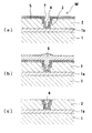
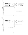
【0003】
図1(a)乃至図1(c)は、この種の銅配線基板Wの一製造例を工程順に示すものである。図1(a)に示すように、半導体素子が形成された半導体基材1上の導電層1aの上にSiO2からなる酸化膜やLow−k材膜などの絶縁膜2が堆積され、リソグラフィ・エッチング技術によりコンタクトホール3と配線用の溝4が形成されている。これらの上にTaN等からなるバリア膜5、更にその上に電解めっきの給電層としてスパッタリングやCVD等によりシード層7が形成されている。
【0004】
そして、基板Wの表面に銅めっきを施すことで、図1(b)に示すように、半導体基材1のコンタクトホール3及び溝4内に銅を充填するとともに、絶縁膜2上に銅膜6を堆積する。その後、化学機械的研磨(CMP)により、絶縁膜2上の銅膜6を除去して、コンタクトホール3及び配線用の溝4に充填させた銅膜6の表面と絶縁膜2の表面とをほぼ同一平面にする。これにより、図1(c)に示すように銅膜6からなる配線が形成される。
【0005】
また、最近ではあらゆる機器の構成要素において微細化かつ高精度化が進み、サブミクロン領域での物作りが一般的となるにつれて、加工法自体が材料の特性に与える影響は益々大きくなっている。このような状況下においては、従来の機械加工のように、工具が被加工物を物理的に破壊しながら除去していく加工方法では、加工によって被加工物に多くの欠陥を生み出してしまうため、被加工物の特性が劣化してしまう。したがって、いかに材料の特性を損なうことなく加工を行うことができるかが問題となってくる。
【0006】
この問題を解決する手段として開発された特殊加工法に、化学研磨や電解加工、電解研磨がある。これらの加工方法は、従来の物理的な加工とは対照的に、化学的溶解反応を起こすことによって、除去加工等を行うものである。したがって、塑性変形による加工変質層や転位等の欠陥は発生せず、上述の材料の特性を損なわずに加工を行うといった課題が達成される。
【0007】
【発明が解決しようとする課題】
例えば、CMP工程は、一般にかなり複雑な操作が必要で、制御も複雑となり、加工時間もかなり長い。更に、研磨後の基板の後洗浄を十分に行う必要があるばかりでなく、スラリーや洗浄液の廃液処理のための負荷が大きい等の課題がある。このため、CMP自体を省略する、あるいはこの負荷を軽減することが強く求められている。また、今後、絶縁膜も誘電率の小さいLow−k材に変わると予想され、このLow−k材は強度が弱くCMPによるストレスに耐えられなくなる。したがって、基板にストレスを与えることなく、平坦化できるようにしたプロセスが望まれている。
【0008】
なお、化学機械的電解研磨のように、めっきをしながらCMPで削るというプロセスも発表されているが、めっき成長面に機械加工が付加されることで、めっきの異常成長を促すことにもなり、膜質に問題を起こしている。
【0009】
本発明は、このような従来技術の問題点に鑑みてなされたもので、例えばCMP処理そのものを省略したり、CMP処理の負荷を極力低減しつつ、基板表面に設けられた導電性材料を平坦に加工したり、更には基板等の被加工物の表面に付着した付着物を除去(洗浄)できるようにした電解加工装置を提供することを目的とする。
【0010】
【課題を解決するための手段】
このような従来技術における問題点を解決するために、本発明の一態様は、加工電極と、被加工物に給電する給電電極と、上記被加工物を保持して上記加工電極に接触又は近接させる保持部と、上記被加工物と上記加工電極又は上記給電電極の少なくとも一方との間に配置されるイオン交換体と、上記加工電極と上記給電電極との間に電圧を印加する電源と、上記イオン交換体が配置された被加工物と加工電極又は給電電極の少なくとも一方との間に流体を供給する流体供給部と、上記保持部で保持した被加工物と上記加工電極とを相対移動させる駆動部とを備え、上記保持部には、少なくとも表面が導電性のダミー部材を上記被加工物の外周側に配置したことを特徴とする電解加工装置である。上記ダミー部材は、上記駆動部による上記被加工物と上記加工電極との相対移動中における該ダミー部材及び上記被加工物と上記加工電極との対面面積を一定にすることが好ましい。
【0011】
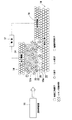
図2及び図3は、本発明の加工原理を示すものである。図2は、被加工物10の表面に、加工電極14に取り付けたイオン交換体12aと、給電電極16に取り付けたイオン交換体12bとを接触又は近接させ、加工電極14と給電電極16との間に電源17を介して電圧を印加しつつ、加工電極14及び給電電極16と被加工物10との間に流体供給部19から超純水等の流体18を供給した状態を示している。図3は、被加工物10の表面に、加工電極14に取り付けたイオン交換体12aを接触又は近接させ、給電電極16を被加工物10に直接接触させて、加工電極14と給電電極16との間に電源17を介して電圧を印加しつつ、加工電極14と被加工物10との間に流体供給部19から超純水等の流体18を供給した状態を示している。
【0012】
超純水のような流体自身の抵抗値が大きい液体を使用する場合には、イオン交換体12aを被加工物10の表面に「接触させる」ことが好ましく、このようにイオン交換体12aを被加工物10の表面に接触させることにより、電気抵抗を低減させることができ、印加電圧も小さくて済み、消費電力も低減できる。したがって、本発明に係る加工における「接触」は、例えばCMPのように物理的なエネルギー(応力)を被加工物に与えるために「押し付ける」ものではない。
【0013】
これにより、超純水等の流体18中の水分子20をイオン交換体12a,12bで水酸化物イオン22と水素イオン24に解離し、例えば生成された水酸化物イオン22を、被加工物10と加工電極14との間の電界と超純水等の流体18の流れによって、被加工物10の加工電極14と対面する表面に供給して、ここでの被加工物10近傍の水酸化物イオン22の密度を高め、被加工物10の原子10aと水酸化物イオン22を反応させる。反応によって生成された反応物質26は、超純水18中に溶解し、被加工物10の表面に沿った超純水等の流体18の流れによって被加工物10から除去される。これにより、被加工物10の表面層の除去加工が行われる。
【0014】
このように、本加工法は純粋に被加工物との電気化学的相互作用のみにより被加工物の除去加工を行うものであり、CMPのような研磨部材と被加工物との物理的な相互作用及び研磨液中の化学種との化学的相互作用の混合による加工とは加工原理が異なるものである。この方法では、被加工物10の加工電極14と対面する部分が加工されるので、加工電極14を移動させることで、被加工物10の表面を所望の表面形状に加工することができる。
【0015】
なお、本発明に係る電解加工装置は、電気化学的相互作用による溶解反応のみにより被加工物の除去加工を行うため、CMPのような研磨部材と被加工物との物理的な相互作用及び研磨液中の化学種との化学的相互作用の混合による加工とは加工原理が異なるものである。したがって、材料の特性を損なわずに除去加工を行うことが可能であり、例えば上述したLow−k材に挙げられる機械的強度の小さい材料に対しても、物理的な相互作用を及ぼすことなく除去加工が可能である。また、通常の電解液を用いる電解加工装置と比較しても、加工液に500μS/cm以下の流体、好ましくは純水、更に好ましくは超純水を用いるため、被加工物表面への汚染も大幅に低減させることが可能であり、また加工後の廃液の処理も容易となる。
【0016】
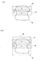
上述したように、本発明では、被加工物10と加工電極14とを相対移動させて被加工物10が加工電極14と対面する部分を移動させることで、被加工物10の全面の加工が行われる。しかしながら、被加工物10及び加工電極14の形状によっては、被加工物10と加工電極14との相対移動に伴い、被加工物10が加工電極14と対面する部分の面積、すなわち対面面積が変化する場合がある。例えば、図4(a)に示す例では、加工電極14が被加工物10に対して相対移動すると、被加工物10の加工電極14と対面する部分の面積がS1からS2に変化する。加工速度は電流密度(=電流値/対面面積)に比例するが、電流値を一定にして加工を行う場合には、対面面積の小さい部分では加工速度が速くなり、大きい部分では加工速度が遅くなる。この結果、被加工物10の全面で加工速度を一定にすることができず、被加工物10に対して均一な加工をすることができない。この場合に、対面面積に応じて電流値を適切に制御して被加工物10の全面で加工速度を均一にすることも考えられるが、加工中に変化する対面面積に応じて電流値を適切に制御することは困難である。
【0017】
本発明では、被加工物の外周側に設けられたダミー部材によって対面面積を一定にすることで均一な加工を実現している。すなわち、図4(b)に示すように、被加工物10の外周側にダミー部材28を設けることによって、加工電極14が被加工物10及びダミー部材28に対面する面積、すなわち対面面積は、被加工物10と加工電極14との相対移動にかかわらず常に一定(S3)となる。したがって、電流値を一定にした場合においても常に電流密度を一定にすることができ、被加工物10の全面において加工速度を一定にして、均一な加工を安定して行うことが可能となる。
【0018】
また、電気化学的な加工においては、反応種であるイオンは、加工電極14と被加工物10(給電電極16)との間に生じる電界によって被加工物10の表面に移動し、このイオンによって被加工物10の表面が加工される。したがって、被加工物10に対して均一な加工を行うためには、加工電極14と被加工物10(給電電極16)との間に生じる電界の強度を被加工物10の全面において均一にすることが必要となる。しかしながら、この電界強度の均一性は、電極や被加工物10の形状によって失われることがある。例えば、図5(a)に示す例では、加工電極14(陰極)と被加工物10(陽極)との間で加工が進行するが、被加工物10の端部においては、端部以外の部分と比べて電気力線(矢印線)及び等電位線(実線)が密になり、電界集中が生じる。このため、被加工物10の端部では反応種であるイオンの量が増加し、加工速度が他の部分と比べて著しく大きくなる。この結果、図5(b)に示すように、被加工物10の端部Aにおいて局所的に加工量が増加し、被加工物10を均一に加工することができない。
【0019】
本発明では、図5(c)に示すように、被加工物10の外周側にダミー部材28を設けているので、上述した電界強度の集中はダミー部材28において生じることとなる。このため、被加工物10の端部における電界強度を他の部分と同じにすることができ、被加工物10の全面において電界強度を一定にすることができる。このように、本発明によれば、被加工物10の全面において加工速度を均一にして、均一な加工を安定して行うことが可能となる。
【0020】
本発明の好ましい一態様は、上記ダミー部材の導電性の部分は、電気化学的に不活性な材質から形成されることを特徴としている。このように、ダミー部材の少なくとも表面を電気化学的に不活性な材質から形成すれば、電解加工中に被加工物とともにダミー部材が加工されてしまうことを防止することができる。
【0021】
本発明の好ましい一態様は、上記ダミー部材の導電性の部分は、上記被加工物と同一の材質から形成されることを特徴としている。このように、ダミー部材の少なくとも表面を被加工物と同一の材質により形成した場合には、ダミー部材における反応を被加工物と同一にすることができるので、加工の均一性をより高めることができる。
【0022】
本発明の好ましい一態様は、上記保持部には、緩衝部材を上記被加工物と上記ダミー部材との間に配置したことを特徴としている。このような緩衝部材により被加工物に対する衝撃を吸収することができる。上記緩衝部材はダミー部材よりも低硬度の材質から形成されていることが好ましい。
【0023】
【発明の実施の形態】
以下、本発明に係る電解加工装置及びこれを組み込んだ基板処理装置の実施形態について図面を参照して詳細に説明する。なお、以下の説明では、被加工物として基板を使用し、電解加工装置で基板を加工するようにした例を示しているが、本発明を基板以外にも適用できることは言うまでもない。
【0024】
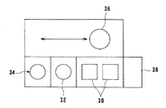
図6は、本発明の第1の実施形態における基板処理装置の構成を示す平面図である。図6に示すように、この基板処理装置は、例えば、図1(b)に示すように、表面に導電体膜(被加工物)としての銅膜6を有する基板Wを収納したカセットを搬出入する搬出入部としての一対のロード・アンロード部30と、基板Wを反転させる反転機32と、電解加工装置34とを備えている。これらの機器は直列に配置されており、これらの機器の間で基板Wを搬送して授受する搬送装置としての搬送ロボット36がこれらの機器と平行に配置されている。また、電解加工装置34による電解加工の際に、後述する加工電極と給電電極との間に印加する電圧又はこれらの間を流れる電流をモニタするモニタ部38がロード・アンロード部30に隣接して配置されている。
【0025】
図7は、基板処理装置内の電解加工装置34を模式的に示す縦断面図である。図7に示すように、電解加工装置34は、上下動可能かつ水平方向に揺動自在なアーム40と、アーム40の自由端に垂設されて基板Wを下向き(フェイスダウン)に吸着保持する基板保持部42と、基板保持部42の下方に配置される円板状の電極部44と、電極部44に接続される電源46とを備えている。本実施形態では、電極部44の大きさは基板保持部42で保持する基板Wの外径よりも一回り大きな大きさに設定されている。
【0026】
アーム40は、揺動用モータ48に連結された揺動軸50の上端に取り付けられており、揺動用モータ48の駆動に伴って水平方向に揺動するようになっている。また、この揺動軸50は、上下方向に延びるボールねじ52に連結されており、ボールねじ52に連結された上下動用モータ54の駆動に伴ってアーム40とともに上下動するようになっている。
【0027】
基板保持部42は、基板保持部42で保持した基板Wと電極部44とを相対移動させる第1駆動部としての自転用モータ56に接続されており、この自転用モータ56の駆動に伴って回転(自転)するようになっている。また、上述したように、アーム40は上下動及び水平方向に揺動可能となっており、基板保持部42はアーム40と一体となって上下動及び水平方向に揺動可能となっている。
【0028】
電極部44の下方には、基板Wと電極部44とを相対移動させる第2駆動部としての中空モータ60が設置されており、この中空モータ60の主軸62には、この主軸62の中心から偏心した位置に駆動端64が設けられている。電極部44は、その中央において上記駆動端64に軸受(図示せず)を介して回転自在に連結されている。また、電極部44と中空モータ60との間には、周方向に3つ以上の自転防止機構が設けられている。
【0029】
図8(a)は本実施形態における自転防止機構を示す平面図、図8(b)は図8(a)のA−A線断面図である。図8(a)及び図8(b)に示すように、電極部44と中空モータ60との間には、周方向に3つ以上(図8(a)においては4つ)の自転防止機構66が設けられている。図8(b)に示すように、中空モータ60の上面と電極部44の下面の対応する位置には、周方向に等間隔に複数の凹所68,70が形成されており、これらの凹所68,70にはそれぞれ軸受72,74が装着されている。軸受72,74には、距離eだけずれた2つの軸体76,78の一端部がそれぞれ挿入されており、軸体76,78の他端部は連結部材80により互いに連結される。ここで、中空モータ60の主軸62の中心に対する駆動端64の偏心量も上述した距離eと同じになっている。したがって、電極部44は、中空モータ60の駆動に伴って、主軸62の中心と駆動端64との間の距離eを半径とした、自転を行わない公転運動、いわゆるスクロール運動(並進回転運動)を行うようになっている。
【0030】
電極部44の中央部には、図7に示すように、純水、より好ましくは超純水を供給する純水供給部としての貫通孔44aが設けられている。この貫通孔44aは、主軸62に形成された貫通孔62aを介して中空モータ60の中空部の内部を延びる純水供給管82に接続されている。このような構成により、電極部44の上面に純水又は超純水が供給されるようになっている。
【0031】
図9は基板保持部42及び電極部44を模式的に示す縦断面図、図10は基板保持部42と電極部44との関係を示す平面図である。図10においては、基板保持部42は点線で示されている。図9及び図10に示すように、電極部44は、円板状の加工電極84と、この加工電極84の周囲を囲繞するリング状の給電電極86と、加工電極84と給電電極86とを分離するリング状の絶縁体88とを備えている。加工電極84の上面はイオン交換体90により、また給電電極86の上面はイオン交換体92によりそれぞれ覆われており、これらのイオン交換体90,92は上記絶縁体88を介して互いに分離されている。
【0032】
本実施形態では、加工電極84を電源46の陰極に接続し、給電電極86を電源46の陽極に接続しているが、加工材料によっては、電源46の陰極に接続される電極を給電電極とし、陽極に接続される電極を加工電極としてもよい。すなわち、被加工材料が例えば銅やモリブデン、鉄である場合には、陰極側に電解加工作用が生じるため、電源46の陰極に接続した電極が加工電極となり、陽極に接続した電極が給電電極となる。一方、被加工材料が例えばアルミニウムやシリコンである場合には、陽極側で電解加工作用が生じるため、電源46の陽極に接続した電極が加工電極となり、陰極に接続した電極が給電電極となる。
【0033】
基板保持部42は、図9に示すように、自転用モータ56に接続されるシャフト94と、シャフト94に連結されるボディ96と、基板Wの外周側に配置される環状のダミー部材98と、ダミー部材98と基板Wとの間に配置される環状の緩衝部材(クッション材)99とを備えている。ダミー部材98の少なくとも表面は、導電性の材質から形成されている。また、基板Wをイオン交換体90,92に接触又は近接させた状態で、基板Wを回転させ、同時に電極部44をスクロール運動させたときに、ダミー部材98の一部が給電電極86及び加工電極84の上方に常に位置するようになっている。
【0034】
ここで、ダミー部材98の導電性の部分の材質としては、一般的な金属や金属化合物の他に、炭素、比較的不活性な貴金属、導電性酸化物又は導電性セラミックスを使用することができ、電気化学的に不活性なものを用いることが好ましい。ダミー部材98に電気化学的に不活性なものを用いた場合には、ダミー部材98は加工されないので、ダミー部材98の長寿命化を図ることができる。また、樹脂などの絶縁物に導電体をコーティングしたもの、例えば、白金などの酸化しにくい材料やイリジウムなどの導電性酸化物で基材の表面を保護したものをダミー部材として用いることもできる。このようなダミー部材は、例えば、チタンの基材の表面にめっきやコーティングで白金又はイリジウムを付着させ、高温で焼結して安定化と強度を保つ処理を行うことにより作製できる。また、セラミックス製品は、一般に無機物質を原料として熱処理によって得られ、各種の非金属・金属の酸化物・炭化物・窒化物などを原料として、様々な特性を持つ製品が作られているが、この中には導電性を有するセラミックスもある。
【0035】
また、ダミー部材98と基板Wとの間に配置された緩衝部材99は、ダミー部材よりも低硬度の材質から形成されており、基板Wに対する衝撃を吸収することができる。この緩衝部材99は、絶縁体であってもよいが、導電体であることが好ましい。
【0036】
次に、本実施形態における基板処理装置を用いた基板処理(電解加工)について説明する。まず、例えば、図1(b)に示すように、表面に導電体膜(被加工部)として銅膜6を形成した基板Wを収納したカセットをロード・アンロード部30にセットし、このカセットから1枚の基板Wを搬送ロボット36で取り出す。搬送ロボット36は、取り出した基板Wを必要に応じて反転機32に搬送し、基板Wの導電体膜(銅膜6)を形成した表面が下を向くように反転させる。
【0037】
搬送ロボット36は反転させた基板Wを受け取り、これを電解加工装置34に搬送し、基板保持部42に吸着保持させる。そして、アーム40を揺動させて基板Wを保持した基板保持部42を電極部44の直上方の加工位置まで移動させる。次に、上下動用モータ54を駆動して基板保持部42を下降させ、この基板保持部42で保持した基板W及びダミー部材98を電極部44のイオン交換体90,92の表面に接触又は近接させる。この状態で、自転用モータ(第1駆動部)56を駆動して基板Wを回転させ、同時に中空モータ60(第2駆動部)を駆動して電極部44をスクロール運動させる。このとき、電極部44の貫通孔44aから基板Wとイオン交換体90,92との間に純水又は超純水を供給する。
【0038】
そして、電源46により加工電極84と給電電極86との間に所定の電圧を印加し、イオン交換体90,92により生成された水素イオン又は水酸化物イオンによって、加工電極(陰極)において基板Wの表面の導電体膜(銅膜6)の電解加工を行う。このとき、加工電極84と対面する部分において加工が進行するが、上述したように、基板Wと加工電極84とを相対移動させることにより基板Wの全面の加工を行っている。本実施形態では、図10に示すように、基板Wの外周側に導電性のダミー部材98を設けているので、加工電極84が基板W及びダミー部材98に対面する面積、すなわち対面面積は、基板Wと加工電極84との相対移動にかかわらず常に一定(斜線部S4)になる。したがって、電流値を一定にした場合においても電流密度を常に一定にすることができ、基板Wの全面において加工速度を一定にして、均一な加工を安定して行うことが可能となる。また、電界強度の集中はダミー部材98において生じることとなるため、基板Wの端部における電界強度を他の部分と同じにすることができる。したがって、被加工物10の全面において電界強度を一定にすることができ、被加工物10の全面において加工速度を均一にして、均一な加工を安定して行うことが可能となる。なお、ダミー部材98を電気化学的に不活性な材質から形成すれば、電解加工中に基板Wとともにダミー部材98が加工されてしまうことを防止することができる。
【0039】
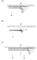
電解加工中には、加工電極と給電電極との間に印加する電圧、又はこの間を流れる電流をモニタ部38でモニタして、エンドポイント(加工終点)を検知する。すなわち、同じ電圧(電流)を印加した状態で電解加工を行うと、材料によって流れる電流(印加される電圧)に違いが生じる。例えば、図11(a)に示すように、表面に材料Bと材料Aとを順次成膜した基板Wの該表面に電解加工を施したときに流れる電流をモニタすると、材料Aを電解加工している間は一定の電流が流れるが、異なる材料Bの加工に移行する時点で流れる電流が変化する。同様に、加工電極と給電電極との間に印加される電圧にあっても、図11(b)に示すように、材料Aを電解加工している間は一定の電圧が印加されるが、異なる材料Bの加工に移行する時点で印加される電圧が変化する。なお、図11(a)は、材料Bを電解加工するときの方が、材料Aを電解加工するときよりも電流が流れにくくなる場合を、図11(b)は、材料Bを電解加工するときの方が、材料Aを電解加工するときよりも電圧が高くなる場合の例を示している。これにより、この電流又は電圧の変化をモニタすることでエンドポイントを確実に検知することができる。
【0040】
なお、モニタ部38で加工電極と給電電極との間に印加する電圧、又はこの間を流れる電流をモニタして加工終点を検知するようにした例を説明したが、このモニタ部38で、加工中の基板の状態の変化をモニタして、任意に設定した加工終点を検知するようにしてもよい。この場合、加工終点は、被加工面の指定した部位について、所望の加工量に達した時点、又は加工量と相関関係を有するパラメータが所望の加工量に相当する量に達した時点を指す。このように、加工の途中においても、加工終点を任意に設定して検知できるようにすることで、多段プロセスでの電解加工が可能となる。
【0041】
電解加工完了後、電源46の接続を切り、基板保持部42の回転と電極部44のスクロール運動を停止させ、しかる後、基板保持部42を上昇させ、アーム40を移動させて基板Wを搬送ロボット36に受け渡す。基板Wを受け取った搬送ロボット36は、必要に応じて反転機32に搬送して反転させた後、基板Wをロード・アンロード部30のカセットに戻す。
【0042】
ここで、電解加工中に基板Wとイオン交換体90,92との間に供給する純水は、例えば電気伝導度が10μS/cm以下の水であり、超純水は、例えば電気伝導度が0.1μS/cm以下の水である。このように電解質を含まない純水又は超純水を使用して電解加工を行うことで、基板Wの表面に電解質等の余分な不純物が付着したり、残留したりすることをなくすことができる。更に、電解によって溶解した銅イオン等が、イオン交換体90,92にイオン交換反応で即座に捕捉されるため、溶解した銅イオン等が基板Wの他の部分に再度析出したり、酸化されて微粒子となり基板Wの表面を汚染したりすることがない。
【0043】
また、純水又は超純水の代わりに電気伝導度500μS/cm以下の液体、例えば純水又は超純水に電解質を添加した電解液を使用してもよい。電解液を使用することで、電気抵抗を低減して消費電力を削減することができる。この電解液としては、例えば、NaClやNa2SO4等の中性塩、HClやH2SO4等の酸、更には、アンモニア等のアルカリなどの溶液を使用することができ、被加工物の特性によって適宜選択して使用することができる。
【0044】
更に、純水又は超純水の代わりに、純水又は超純水に界面活性剤等を添加して、電気伝導度が500μS/cm以下、好ましくは、50μS/cm以下、更に好ましくは、0.1μS/cm以下(比抵抗で10MΩ・cm以上)にした液体を使用してもよい。このように、純水又は超純水に界面活性剤を添加することで、基板Wとイオン交換体90,92の界面にイオンの移動を防ぐ一様な抑制作用を有する層を形成し、これによって、イオン交換(金属の溶解)の集中を緩和して被加工面の平坦性を向上させることができる。ここで、界面活性剤濃度は、100ppm以下が好ましい。なお、電気伝導度の値が高すぎると電流効率が下がり、加工速度が遅くなるが、500μS/cm以下、好ましくは、50μS/cm以下、更に好ましくは、0.1μS/cm以下の電気伝導度を有する液体を使用することで、所望の加工速度を得ることができる。
【0045】
また、電極部44のイオン交換体90,92は、例えば、アニオン交換能又はカチオン交換能を付与した不織布で構成することができる。カチオン交換体は、好ましくは強酸性カチオン交換基(スルホン酸基)を担持したものであるが、弱酸性カチオン交換基(カルボキシル基)を担持したものでもよい。また、アニオン交換体は、好ましくは強塩基性アニオン交換基(4級アンモニウム基)を担持したものであるが、弱塩基性アニオン交換基(3級以下のアミノ基)を担持したものでもよい。
【0046】
ここで、例えば強塩基アニオン交換能を付与した不織布は、繊維径20〜50μmで空隙率が約90%のポリオレフィン製の不織布に、γ線を照射した後グラフト重合を行う所謂放射線グラフト重合法により、グラフト鎖を導入し、次に導入したグラフト鎖をアミノ化して第4級アンモニウム基を導入して作製される。導入されるイオン交換基の容量は、導入するグラフト鎖の量により決定される。グラフト重合を行うためには、例えばアクリル酸、スチレン、メタクリル酸グリシジル、更にはスチレンスルホン酸ナトリウム、クロロメチルスチレン等のモノマーを用い、これらのモノマー濃度、反応温度及び反応時間を制御することで、重合するグラフト量を制御することができる。したがって、グラフト重合前の素材の重量に対し、グラフト重合後の重量の比をグラフト率と呼ぶが、このグラフト率は、最大で500%が可能であり、グラフト重合後に導入されるイオン交換基は、最大で5meq/gが可能である。
【0047】
強酸性カチオン交換能を付与した不織布は、上記強塩基性アニオン交換能を付与する方法と同様に、繊維径20〜50μmで空隙率が約90%のポリオレフィン製の不織布に、γ線を照射した後グラフト重合を行う所謂放射線グラフト重合法により、グラフト鎖を導入し、次に導入したグラフト鎖を、例えば加熱した硫酸で処理してスルホン酸基を導入して作製される。また、加熱したリン酸で処理すればリン酸基が導入できる。ここでグラフト率は、最大で500%が可能であり、グラフト重合後に導入されるイオン交換基は、最大で5meq/gが可能である。
【0048】
なお、イオン交換体90,92の素材の材質としては、ポリエチレン、ポリプロピレン等のポリオレフィン系高分子、又はその他有機高分子が挙げられる。また素材形態としては、不織布の他に、織布、シート、多孔質材、短繊維等が挙げられる。ここで、ポリエチレンやポリプロピレンは、放射線(γ線と電子線)を先に素材に照射する(前照射)ことで、素材にラジカルを発生させ、次にモノマーと反応させてグラフト重合することができる。これにより、均一性が高く、不純物が少ないグラフト鎖ができる。一方、その他の有機高分子は、モノマーを含浸させ、そこに放射線(γ線、電子線、紫外線)を照射(同時照射)することで、ラジカル重合することができる。この場合、均一性に欠けるが、ほとんどの素材に適用できる。
【0049】
このように、イオン交換体90,92をアニオン交換能又はカチオン交換能を付与した不織布で構成することで、純水又は超純水や電解液等の液体が不織布の内部を自由に移動して、不織布内部の水分解触媒作用を有する活性点に容易に到達することが可能となって、多くの水分子が水素イオンと水酸化物イオンに解離される。更に、解離によって生成した水酸化物イオンが純水又は超純水や電解液等の液体の移動に伴って効率良く加工電極84の表面に運ばれるため、低い印加電圧でも高電流が得られる。
【0050】
ここで、イオン交換体90,92をアニオン交換能又はカチオン交換能の一方を付与したもののみで構成すると、電解加工できる被加工材料が制限されるばかりでなく、極性により不純物が生成しやすくなる。そこで、アニオン交換能を有するアニオン交換体とカチオン交換能を有するカチオン交換体とを重ね合わせたり、イオン交換体90,92自体にアニオン交換能とカチオン交換能の双方の交換基を付与するようにしたりしてもよく、これにより、被加工材料の範囲を拡げるとともに、不純物を生成しにくくすることができる。
【0051】
また、電極は、電解反応により酸化又は溶出が一般に問題となる。このため、電極の素材として、ダミー部材98と同様に、炭素、比較的不活性な貴金属、導電性酸化物又は導電性セラミックスを使用することが好ましい。電極が酸化すると電極の電気抵抗値が増加し、印加電圧の上昇を招くが、白金などの酸化しにくい材料やイリジウムなどの導電性酸化物で電極表面を保護すれば、電極素材の酸化による導電性の低下を防止することができる。
【0052】
上述の実施形態では、ダミー部材98を電気化学的に不活性な材質により形成した例を説明したが、ダミー部材98を基板Wと同一の材質により形成してもよい。ダミー部材98を電気化学的に不活性な材質で形成した場合には、ダミー部材98の材質によっては、ダミー部材98に基板Wとは別の反応が生じて均一性が損なわれる場合も考えられる。これに対して、ダミー部材98を基板Wと同一の材質により形成した場合には、ダミー部材98における反応を基板Wと同一にすることができるので、加工の均一性をより高めることができる。
【0053】
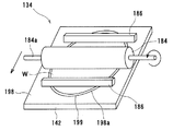
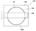
図12は本発明の第2の実施形態における電解加工装置を模式的に示す斜視図、図13は図12の平面図である。本実施形態における電解加工装置134は、基板Wを上向き(フェイスアップ)に保持する基板保持部142と、基板保持部142の上方に配置された円筒状の加工電極184と、基板保持部142の上方に配置された2つの給電電極186(図13においては図示せず)とを備えている。また、基板保持部142は、基板Wを収容する凹部198aが形成された矩形状のダミー部材198と、ダミー部材198と基板Wとの間に配置された緩衝部材199とを備えている。
【0054】
各給電電極186は、基板Wとダミー部材198とに跨って配置されており、基板Wとダミー部材198の双方に接触している。加工電極184の表面にはイオン交換体が貼付されており、図示しない駆動部により軸184aを中心に回転するようになっている。この加工電極184は、基板Wに接触又は近接した状態で基板W上をスキャンできるようになっている。
【0055】
このような構成において、図示しない純水供給部から基板Wと加工電極184のイオン交換体との間に純水又は超純水を供給しつつ、駆動部により加工電極184を基板Wに接触又は近接させた状態で一方向に移動させる。これによって、基板Wの表面の電解加工が行われるようになっている。
【0056】
本実施形態においても、図13に示すように、加工電極184が基板W及びダミー部材198に対面する面積(対面面積)は、基板Wと加工電極184との相対移動にかかわらず一定になる。したがって、電流値を一定にした場合においても電流密度を常に一定にすることができ、基板Wの全面において加工速度を一定にして、均一な加工を安定して行うことが可能となる。
【0057】
これまで本発明の一実施形態について説明したが、本発明は上述の実施形態に限定されず、その技術的思想の範囲内において種々異なる形態にて実施されてよいことは言うまでもない。
【0058】
【発明の効果】
上述したように、本発明によれば、基板等の被加工物に物理的な欠陥を与えて被加工物の特性を損なうことを防止しつつ、電気化学的作用によって、例えばCMPに代わる電解加工等を施すことができ、これによって、CMP処理そのものを省略したり、CMP処理の負荷を低減したり、更には基板等の被加工物の表面に付着した付着物を除去(洗浄)することができる。しかも、純水又は超純水のみを使用しても基板を加工することができ、これによって、基板の表面に電解質等の余分な不純物の付着したり、残留したりすることをなくして、加工除去加工後の洗浄工程を簡略化できるばかりでなく、廃液処理の負荷を極めて小さくすることができる。
【図面の簡単な説明】
【図1】銅配線基板の一製造例を工程順に示す図である。
【図2】加工電極及び給電電極を基板(被加工物)に近接させ、加工電極及び給電電極と基板(被加工物)との間に純水又は電気伝導度が500μS/cm以下の液体を供給するようにしたときの本発明による電解加工の原理の説明に付する図である。
【図3】加工電極のみにイオン交換体を取り付けて、加工電極と基板(被加工物)との間に液体を供給するようにしたときの本発明による電解加工の原理の説明に付する図である。
【図4】図4(a)はダミー部材を設けない場合の対面面積の説明に付する図、図4(b)はダミー部材を設けた場合の対面面積の説明に付する図である。
【図5】図5(a)はダミー部材を設けない場合の電界強度の説明に付する図、図5(b)は図5(a)の場合の加工後の被加工物を示す図、図5(c)はダミー部材を設けた場合の電界強度の説明に付する図である。
【図6】本発明の第1の実施形態における基板処理装置の構成を示す平面図である。
【図7】図6に示す基板処理装置の電解加工装置を模式的に示す縦断面図である。
【図8】図8(a)は図7の電解加工装置における自転防止機構を示す平面図、図8(b)は図8(a)のA−A線断面図である。
【図9】図7の電解加工装置における基板保持部及び電極部を模式的に示す縦断面図である。
【図10】図9の基板保持部と電極部との関係を示す平面図である。
【図11】図11(a)は、異なる材料を成膜した基板の表面に電解加工を施したときに流れる電流と時間の関係を、図11(b)は、同じく印加される電圧と時間の関係をそれぞれ示すグラフである。
【図12】本発明の第2の実施形態における電解加工装置を模式的に示す斜視図である。
【図13】図12の平面図である。
【符号の説明】
6 銅膜(導電体膜)
7 シード層
10 被加工物
12a,12b イオン交換体
14 加工電極
16 給電電極
17 電源
18 超純水
19 流体供給部
20 水分子
22 水酸化物イオン
24 水素イオン
26 反応物質
28 ダミー部材
30 ロード・アンロード部
32 反転機
34,134 電解加工装置
36 搬送ロボット
38 モニタ部
40 アーム
42,142 基板保持部
44 電極部
44a 貫通孔
46 電源
48 揺動用モータ
50 揺動軸
52 ボールねじ
54 上下動用モータ
56 自転用モータ
60 中空モータ
62 主軸
64 駆動端
66 自転防止機構
68,70 凹所
72,74 軸受
76,78 軸体
80 連結部材
82 純水供給管
84,184 加工電極
86,186 給電電極
88 絶縁体
90,92 イオン交換体
94 シャフト
96 ボディ
98,198 ダミー部材
99,199 緩衝部材[0001]
BACKGROUND OF THE INVENTION
The present invention relates to an electrolytic processing apparatus, and more particularly to an electrolytic processing apparatus used for processing a conductive material formed on the surface of a substrate such as a semiconductor wafer or removing impurities adhering to the surface of the substrate. It is about.
[0002]
[Prior art]
In recent years, as a wiring material for forming a circuit on a substrate such as a semiconductor wafer, the movement of using copper (Cu) having a low electrical resistivity and a high electromigration resistance in place of aluminum or an aluminum alloy has become prominent. . This type of copper wiring is generally formed by embedding copper in a fine recess provided on the surface of the substrate. As a method of forming this copper wiring, there is a method such as chemical vapor deposition (CVD), sputtering and plating, but in any case, copper is formed on almost the entire surface of the substrate, Unnecessary copper is removed by chemical mechanical polishing (CMP).
[0003]
FIG. 1A to FIG. 1C show a manufacturing example of this type of copper wiring board W in the order of steps. As shown in FIG. 1A, SiO is formed on a
[0004]
Then, by copper plating on the surface of the substrate W, as shown in FIG. 1B, the
[0005]
In recent years, as the miniaturization and high precision have progressed in the components of all devices, and the manufacturing in the submicron region has become common, the influence of the processing method itself on the characteristics of the material has been increasing. Under such circumstances, the machining method in which the tool removes the workpiece while physically destroying it, as in conventional machining, because many defects are generated in the workpiece by machining. As a result, the properties of the workpiece are deteriorated. Therefore, it becomes a problem how the processing can be performed without impairing the characteristics of the material.
[0006]
Special processing methods developed as means for solving this problem include chemical polishing, electrolytic processing, and electrolytic polishing. In contrast to conventional physical processing, these processing methods perform removal processing and the like by causing a chemical dissolution reaction. Therefore, defects such as work-affected layers and dislocations due to plastic deformation do not occur, and the problem of performing processing without impairing the properties of the above-described materials is achieved.
[0007]
[Problems to be solved by the invention]
For example, the CMP process generally requires a considerably complicated operation, is complicated in control, and has a considerably long processing time. Furthermore, not only is it necessary to sufficiently perform post-cleaning of the substrate after polishing, but there are also problems such as a large load for waste liquid treatment of slurry and cleaning liquid. Therefore, there is a strong demand for omitting CMP itself or reducing this load. In the future, it is expected that the insulating film will also be changed to a low-k material having a low dielectric constant. This low-k material is weak in strength and cannot withstand the stress caused by CMP. Therefore, there is a demand for a process that can be planarized without applying stress to the substrate.
[0008]
In addition, a process of cutting by CMP while plating, such as chemical mechanical electropolishing, has been announced, but by adding machining to the plating growth surface, it will also promote abnormal growth of plating. , Causing problems with film quality.
[0009]
The present invention has been made in view of such problems of the prior art. For example, the conductive material provided on the substrate surface is flattened while omitting the CMP process itself or reducing the load of the CMP process as much as possible. It is another object of the present invention to provide an electrolytic processing apparatus that can process (or wash) deposits adhered to the surface of a workpiece such as a substrate.
[0010]
[Means for Solving the Problems]
In order to solve such problems in the prior art, one embodiment of the present invention includes a machining electrode, a power feeding electrode that feeds power to the workpiece, and a contact or proximity of the machining electrode that holds the workpiece. A holding part, an ion exchanger disposed between the workpiece and at least one of the processing electrode or the power feeding electrode, a power source for applying a voltage between the processing electrode and the power feeding electrode, A fluid supply unit that supplies a fluid between a workpiece on which the ion exchanger is disposed and at least one of a processing electrode or a feeding electrode, and a relative movement between the workpiece and the processing electrode held by the holding unit The electrolytic processing apparatus is characterized in that at least a conductive dummy member having a surface is disposed on the outer peripheral side of the workpiece. The dummy member is being moved relative to the workpiece and the machining electrode by the driving unit. Between the dummy member and the workpiece and the machining electrode It is preferable to make the facing area constant.
[0011]
2 and 3 show the processing principle of the present invention. In FIG. 2, an
[0012]
When using a liquid having a high resistance value, such as ultrapure water, it is preferable to “contact” the
[0013]
Thereby, the
[0014]
As described above, this processing method purely performs the removal processing of the work piece only by the electrochemical interaction with the work piece, and the physical interaction between the polishing member such as CMP and the work piece. The processing principle is different from processing by mixing action and chemical interaction with chemical species in the polishing liquid. In this method, since the portion of the
[0015]
In addition, since the electrolytic processing apparatus according to the present invention performs removal processing of a workpiece only by a dissolution reaction by electrochemical interaction, physical interaction and polishing between a polishing member such as CMP and the workpiece. The processing principle is different from processing by mixing chemical interaction with chemical species in the liquid. Therefore, it is possible to perform removal processing without damaging the properties of the material. For example, even a material with low mechanical strength, such as the Low-k material described above, can be removed without causing physical interaction. Processing is possible. Further, even when compared with an electrolytic processing apparatus using a normal electrolytic solution, a fluid of 500 μS / cm or less, preferably pure water, and more preferably ultrapure water is used as the processing solution, so that contamination on the surface of the workpiece is also caused. It can be greatly reduced, and processing of waste liquid after processing becomes easy.
[0016]
As described above, in the present invention, the entire surface of the
[0017]
In the present invention, uniform processing is realized by making the facing area constant by a dummy member provided on the outer peripheral side of the workpiece. That is, as shown in FIG. 4B, by providing the
[0018]
In electrochemical machining, ions that are reactive species move to the surface of the
[0019]
In the present invention, as shown in FIG. 5C, since the
[0020]
In a preferred aspect of the present invention, the conductive portion of the dummy member is formed of an electrochemically inactive material. Thus, if at least the surface of the dummy member is formed of an electrochemically inactive material, it is possible to prevent the dummy member from being processed together with the workpiece during electrolytic processing.
[0021]
In a preferred aspect of the present invention, the conductive portion of the dummy member is formed of the same material as the workpiece. As described above, when at least the surface of the dummy member is formed of the same material as the workpiece, the reaction in the dummy member can be made the same as that of the workpiece, so that the processing uniformity can be further improved. it can.
[0022]
In a preferred aspect of the present invention, the holding part is characterized in that a buffer member is disposed between the workpiece and the dummy member. Such a buffer member can absorb an impact on the workpiece. The buffer member is preferably formed of a material having a lower hardness than the dummy member.
[0023]
DETAILED DESCRIPTION OF THE INVENTION
Embodiments of an electrolytic processing apparatus and a substrate processing apparatus incorporating the same according to the present invention will be described below in detail with reference to the drawings. In the following description, an example is shown in which a substrate is used as a workpiece and the substrate is processed by an electrolytic processing apparatus, but it goes without saying that the present invention can be applied to other than the substrate.
[0024]
FIG. 6 is a plan view showing the configuration of the substrate processing apparatus according to the first embodiment of the present invention. As shown in FIG. 6, this substrate processing apparatus carries out, for example, a cassette containing a substrate W having a
[0025]
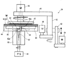
FIG. 7 is a longitudinal sectional view schematically showing the
[0026]
The
[0027]
The
[0028]
A
[0029]
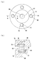
FIG. 8A is a plan view showing the rotation prevention mechanism in the present embodiment, and FIG. 8B is a cross-sectional view taken along line AA of FIG. As shown in FIGS. 8A and 8B, there are three or more rotation prevention mechanisms (four in FIG. 8A) in the circumferential direction between the
[0030]
As shown in FIG. 7, a through-
[0031]
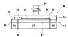
FIG. 9 is a longitudinal sectional view schematically showing the
[0032]
In this embodiment, the
[0033]
As shown in FIG. 9, the
[0034]
Here, as a material of the conductive portion of the
[0035]
Further, the
[0036]
Next, substrate processing (electrolytic processing) using the substrate processing apparatus in the present embodiment will be described. First, for example, as shown in FIG. 1B, a cassette containing a substrate W on which a
[0037]
The
[0038]
Then, a predetermined voltage is applied between the processing
[0039]
During the electrolytic machining, the voltage applied between the machining electrode and the feeding electrode or the current flowing therebetween is monitored by the
[0040]
In addition, although the
[0041]
After completion of the electrolytic processing, the
[0042]
Here, pure water supplied between the substrate W and the
[0043]
Instead of pure water or ultrapure water, a liquid having an electric conductivity of 500 μS / cm or less, for example, an electrolytic solution obtained by adding an electrolyte to pure water or ultrapure water may be used. By using the electrolytic solution, electric resistance can be reduced and power consumption can be reduced. Examples of the electrolytic solution include NaCl and Na 2 SO 4 Neutral salt such as HCl and H 2 SO 4 A solution such as an acid such as ammonia or an alkali such as ammonia can be used, and can be selected and used as appropriate depending on the properties of the workpiece.
[0044]
Furthermore, instead of pure water or ultrapure water, a surfactant or the like is added to pure water or ultrapure water, and the electric conductivity is 500 μS / cm or less, preferably 50 μS / cm or less, more preferably 0. A liquid having a specific resistance of 10 MΩ · cm or less may be used. In this way, by adding a surfactant to pure water or ultrapure water, a layer having a uniform suppressing action for preventing the movement of ions is formed at the interface between the substrate W and the
[0045]
Moreover, the
[0046]
Here, for example, a nonwoven fabric imparted with a strong base anion exchange ability is a so-called radiation graft polymerization method in which a polyolefin nonwoven fabric having a fiber diameter of 20 to 50 μm and a porosity of about 90% is irradiated with γ rays and then graft polymerization is performed. The graft chain is introduced, and then the introduced graft chain is aminated to introduce a quaternary ammonium group. The capacity of the ion exchange group to be introduced is determined by the amount of graft chains to be introduced. In order to perform the graft polymerization, for example, using monomers such as acrylic acid, styrene, glycidyl methacrylate, sodium styrenesulfonate, chloromethylstyrene, and the like, by controlling the monomer concentration, reaction temperature, and reaction time, The amount of grafting to be polymerized can be controlled. Therefore, the ratio of the weight after graft polymerization to the weight of the material before graft polymerization is called the graft ratio. This graft ratio can be up to 500%, and the ion exchange groups introduced after the graft polymerization are A maximum of 5 meq / g is possible.
[0047]
The nonwoven fabric imparted with strong acid cation exchange ability was irradiated with γ-rays on a polyolefin nonwoven fabric having a fiber diameter of 20 to 50 μm and a porosity of about 90% in the same manner as the method for imparting strong basic anion exchange ability. A graft chain is introduced by a so-called radiation graft polymerization method in which post-graft polymerization is performed, and then the introduced graft chain is treated with, for example, heated sulfuric acid to introduce a sulfonic acid group. Moreover, a phosphoric acid group can be introduce | transduced if it processes with the heated phosphoric acid. Here, the graft ratio can be 500% at the maximum, and the ion exchange group introduced after the graft polymerization can be 5 meq / g at the maximum.
[0048]
Examples of the material of the
[0049]
In this way, by configuring the
[0050]
Here, if the
[0051]
In addition, oxidation or elution of the electrode generally causes a problem due to an electrolytic reaction. For this reason, as with the
[0052]
In the above-described embodiment, the example in which the
[0053]
FIG. 12 is a perspective view schematically showing an electrolytic processing apparatus according to the second embodiment of the present invention, and FIG. 13 is a plan view of FIG. The
[0054]
Each
[0055]
In such a configuration, while supplying pure water or ultrapure water between the substrate W and the ion exchanger of the
[0056]
Also in this embodiment, as shown in FIG. 13, the area (facing area) where the
[0057]
Although one embodiment of the present invention has been described so far, it is needless to say that the present invention is not limited to the above-described embodiment, and may be implemented in various forms within the scope of the technical idea.
[0058]
【The invention's effect】
As described above, according to the present invention, an electrochemical process, for example, in place of CMP, is performed by electrochemical action while preventing physical damage to a workpiece such as a substrate and damaging the properties of the workpiece. As a result, the CMP process itself can be omitted, the load of the CMP process can be reduced, and the deposits attached to the surface of the workpiece such as the substrate can be removed (cleaned). it can. Moreover, the substrate can be processed even using pure water or ultrapure water alone, thereby eliminating the need for extra impurities such as electrolytes to remain on the surface of the substrate or remaining. Not only can the cleaning process after removal processing be simplified, but also the waste liquid treatment load can be extremely reduced.
[Brief description of the drawings]
FIG. 1 is a diagram showing an example of manufacturing a copper wiring board in the order of processes.
FIG. 2 shows that a processing electrode and a feeding electrode are brought close to a substrate (workpiece), and pure water or a liquid having an electric conductivity of 500 μS / cm or less is placed between the processing electrode and the feeding electrode and the substrate (workpiece). It is a figure attached | subjected to description of the principle of the electrolytic processing by this invention when it was made to supply.
FIG. 3 is a diagram for explaining the principle of electrolytic processing according to the present invention when an ion exchanger is attached only to a processing electrode and liquid is supplied between the processing electrode and a substrate (workpiece). It is.
4A is a diagram for explaining the facing area when a dummy member is not provided, and FIG. 4B is a diagram for explaining the facing area when a dummy member is provided.
5A is a diagram for explaining the electric field strength when a dummy member is not provided, and FIG. 5B is a diagram showing a workpiece after processing in the case of FIG. 5A; FIG.5 (c) is a figure attached to description of the electric field strength at the time of providing a dummy member.
FIG. 6 is a plan view showing the configuration of the substrate processing apparatus according to the first embodiment of the present invention.
7 is a longitudinal sectional view schematically showing an electrolytic processing apparatus of the substrate processing apparatus shown in FIG.
8 (a) is a plan view showing a rotation prevention mechanism in the electrolytic processing apparatus of FIG. 7, and FIG. 8 (b) is a cross-sectional view taken along line AA of FIG. 8 (a).
9 is a longitudinal sectional view schematically showing a substrate holding part and an electrode part in the electrolytic processing apparatus of FIG.
10 is a plan view showing the relationship between the substrate holding part and the electrode part in FIG. 9;
FIG. 11 (a) shows the relationship between current and time flowing when electrolytic processing is performed on the surface of a substrate on which different materials are formed, and FIG. 11 (b) shows the same applied voltage and time. It is a graph which shows each relationship.
FIG. 12 is a perspective view schematically showing an electrolytic processing apparatus according to a second embodiment of the present invention.
FIG. 13 is a plan view of FIG.
[Explanation of symbols]
6 Copper film (conductor film)
7 Seed layer
10 Workpiece
12a, 12b ion exchanger
14 Processing electrode
16 Feeding electrode
17 Power supply
18 Ultrapure water
19 Fluid supply unit
20 water molecules
22 Hydroxide ion
24 Hydrogen ion
26 Reactant
28 Dummy parts
30 Load / Unload Club
32 reversing machine
34,134 Electrolytic processing equipment
36 Transfer robot
38 Monitor section
40 arms
42,142 Substrate holder
44 Electrode section
44a Through hole
46 Power supply
48 Swing motor
50 Oscillating shaft
52 Ball screw
54 Motor for vertical movement
56 Motor for rotation
60 Hollow motor
62 Spindle
64 Drive end
66 Anti-rotation mechanism
68,70 recess
72,74 bearings
76,78 shaft
80 connecting members
82 Pure water supply pipe
84,184 machining electrode
86,186 Feed electrode
88 Insulator
90,92 ion exchanger
94 shaft
96 body
98,198 Dummy
99,199 cushioning member
Claims (5)
被加工物に給電する給電電極と、
前記被加工物を保持して前記加工電極に接触又は近接させる保持部と、
前記被加工物と前記加工電極又は前記給電電極の少なくとも一方との間に配置されるイオン交換体と、
前記加工電極と前記給電電極との間に電圧を印加する電源と、
前記イオン交換体が配置された被加工物と加工電極又は給電電極の少なくとも一方との間に流体を供給する流体供給部と、
前記保持部で保持した被加工物と前記加工電極とを相対移動させる駆動部とを備え、
前記保持部には、少なくとも表面が導電性のダミー部材を前記被加工物の外周側に配置したことを特徴とする電解加工装置。A machining electrode;
A power supply electrode for supplying power to the workpiece;
A holding unit that holds the workpiece and contacts or approaches the processing electrode;
An ion exchanger disposed between the workpiece and at least one of the processing electrode or the feeding electrode;
A power source for applying a voltage between the machining electrode and the power supply electrode;
A fluid supply unit for supplying a fluid between a workpiece on which the ion exchanger is disposed and at least one of a processing electrode or a feeding electrode;
A drive unit that relatively moves the workpiece held by the holding unit and the machining electrode;
An electrolytic processing apparatus, wherein a dummy member having at least a conductive surface is disposed on the outer peripheral side of the workpiece in the holding portion.
Priority Applications (7)
| Application Number | Priority Date | Filing Date | Title |
|---|---|---|---|
| JP2002112487A JP4127361B2 (en) | 2002-04-15 | 2002-04-15 | Electrolytic processing equipment |
| TW092102160A TWI277473B (en) | 2002-01-31 | 2003-01-30 | Electrolytic processing apparatus and method, fixing method, fixing structure for ion exchanging member |
| KR10-2004-7011804A KR20040083103A (en) | 2002-01-31 | 2003-01-31 | Electrolytic processing apparatus and method |
| EP03734903A EP1470269A4 (en) | 2002-01-31 | 2003-01-31 | Electrolytic processing apparatus and method |
| US10/485,204 US7655118B2 (en) | 2002-01-31 | 2003-01-31 | Electrolytic processing apparatus and method |
| CNB038028883A CN100346009C (en) | 2002-01-31 | 2003-01-31 | Electrolytic processing apparatus and method |
| PCT/JP2003/001011 WO2003064734A1 (en) | 2002-01-31 | 2003-01-31 | Electrolytic processing apparatus and method |
Applications Claiming Priority (1)
| Application Number | Priority Date | Filing Date | Title |
|---|---|---|---|
| JP2002112487A JP4127361B2 (en) | 2002-04-15 | 2002-04-15 | Electrolytic processing equipment |
Publications (2)
| Publication Number | Publication Date |
|---|---|
| JP2003305615A JP2003305615A (en) | 2003-10-28 |
| JP4127361B2 true JP4127361B2 (en) | 2008-07-30 |
Family
ID=29394978
Family Applications (1)
| Application Number | Title | Priority Date | Filing Date |
|---|---|---|---|
| JP2002112487A Expired - Fee Related JP4127361B2 (en) | 2002-01-31 | 2002-04-15 | Electrolytic processing equipment |
Country Status (1)
| Country | Link |
|---|---|
| JP (1) | JP4127361B2 (en) |
-
2002
- 2002-04-15 JP JP2002112487A patent/JP4127361B2/en not_active Expired - Fee Related
Also Published As
| Publication number | Publication date |
|---|---|
| JP2003305615A (en) | 2003-10-28 |
Similar Documents
| Publication | Publication Date | Title |
|---|---|---|
| US7655118B2 (en) | Electrolytic processing apparatus and method | |
| CN100449705C (en) | Electrolytic treatment device and substrate processing equipment | |
| US20070187259A1 (en) | Substrate processing apparatus and method | |
| US7101465B2 (en) | Electrolytic processing device and substrate processing apparatus | |
| US20060091005A1 (en) | Electolytic processing apparatus | |
| JP3933520B2 (en) | Substrate processing apparatus and substrate processing method | |
| JP4127361B2 (en) | Electrolytic processing equipment | |
| JP4310085B2 (en) | Electrolytic machining method and apparatus | |
| US20040256237A1 (en) | Electrolytic processing apparatus and method | |
| JP4233331B2 (en) | Electrolytic machining method and apparatus | |
| JP4172945B2 (en) | Method and apparatus for regenerating ion exchanger for electrolytic processing | |
| JP4130073B2 (en) | Ion exchanger regeneration method and regeneration apparatus | |
| JP4409807B2 (en) | Substrate processing method | |
| JP2004002910A (en) | Electrolytic working method and apparatus | |
| JP2003080421A (en) | Electrochemical machining device | |
| US7563356B2 (en) | Composite processing apparatus and method | |
| JP2007284795A (en) | Electrode structure and electrolytic processing device | |
| JP2005199401A (en) | Electrochemical machining device and method | |
| JP2003175422A (en) | Electrochemical machining device and electrochemical machining method | |
| JP2004255479A (en) | Electrochemical machining method and electrochemical machining device | |
| JP2004084054A (en) | Electrolytic processing method and device | |
| JP2006009103A (en) | Electrolytic processing apparatus and method for conditioning contact member | |
| JP2005054205A (en) | Electrochemical machining apparatus and electrochemical machining method | |
| JP2006013177A (en) | Apparatus and method for electrolytic processing | |
| JP2006002245A (en) | Electrolytic processing apparatus and electrolytic processing method |
Legal Events
| Date | Code | Title | Description |
|---|---|---|---|
| A621 | Written request for application examination |
Free format text: JAPANESE INTERMEDIATE CODE: A621 Effective date: 20050127 |
|
| A131 | Notification of reasons for refusal |
Free format text: JAPANESE INTERMEDIATE CODE: A131 Effective date: 20080122 |
|
| A521 | Written amendment |
Free format text: JAPANESE INTERMEDIATE CODE: A523 Effective date: 20080318 |
|
| TRDD | Decision of grant or rejection written | ||
| A01 | Written decision to grant a patent or to grant a registration (utility model) |
Free format text: JAPANESE INTERMEDIATE CODE: A01 Effective date: 20080507 |
|
| A01 | Written decision to grant a patent or to grant a registration (utility model) |
Free format text: JAPANESE INTERMEDIATE CODE: A01 |
|
| A61 | First payment of annual fees (during grant procedure) |
Free format text: JAPANESE INTERMEDIATE CODE: A61 Effective date: 20080507 |
|
| FPAY | Renewal fee payment (event date is renewal date of database) |
Free format text: PAYMENT UNTIL: 20110523 Year of fee payment: 3 |
|
| R150 | Certificate of patent or registration of utility model |
Free format text: JAPANESE INTERMEDIATE CODE: R150 |
|
| FPAY | Renewal fee payment (event date is renewal date of database) |
Free format text: PAYMENT UNTIL: 20110523 Year of fee payment: 3 |
|
| FPAY | Renewal fee payment (event date is renewal date of database) |
Free format text: PAYMENT UNTIL: 20120523 Year of fee payment: 4 |
|
| FPAY | Renewal fee payment (event date is renewal date of database) |
Free format text: PAYMENT UNTIL: 20130523 Year of fee payment: 5 |
|
| LAPS | Cancellation because of no payment of annual fees |