JP4108623B2 - Liquid crystal display device and driving method thereof - Google Patents
Liquid crystal display device and driving method thereof Download PDFInfo
- Publication number
- JP4108623B2 JP4108623B2 JP2004042014A JP2004042014A JP4108623B2 JP 4108623 B2 JP4108623 B2 JP 4108623B2 JP 2004042014 A JP2004042014 A JP 2004042014A JP 2004042014 A JP2004042014 A JP 2004042014A JP 4108623 B2 JP4108623 B2 JP 4108623B2
- Authority
- JP
- Japan
- Prior art keywords
- liquid crystal
- signal
- driving
- counter electrode
- input
- Prior art date
- Legal status (The legal status is an assumption and is not a legal conclusion. Google has not performed a legal analysis and makes no representation as to the accuracy of the status listed.)
- Expired - Fee Related
Links
Images


Classifications
-
- G—PHYSICS
- G09—EDUCATION; CRYPTOGRAPHY; DISPLAY; ADVERTISING; SEALS
- G09F—DISPLAYING; ADVERTISING; SIGNS; LABELS OR NAME-PLATES; SEALS
- G09F3/00—Labels, tag tickets, or similar identification or indication means; Seals; Postage or like stamps
- G09F3/08—Fastening or securing by means not forming part of the material of the label itself
- G09F3/10—Fastening or securing by means not forming part of the material of the label itself by an adhesive layer
-
- G—PHYSICS
- G09—EDUCATION; CRYPTOGRAPHY; DISPLAY; ADVERTISING; SEALS
- G09G—ARRANGEMENTS OR CIRCUITS FOR CONTROL OF INDICATING DEVICES USING STATIC MEANS TO PRESENT VARIABLE INFORMATION
- G09G3/00—Control arrangements or circuits, of interest only in connection with visual indicators other than cathode-ray tubes
- G09G3/20—Control arrangements or circuits, of interest only in connection with visual indicators other than cathode-ray tubes for presentation of an assembly of a number of characters, e.g. a page, by composing the assembly by combination of individual elements arranged in a matrix no fixed position being assigned to or needed to be assigned to the individual characters or partial characters
- G09G3/34—Control arrangements or circuits, of interest only in connection with visual indicators other than cathode-ray tubes for presentation of an assembly of a number of characters, e.g. a page, by composing the assembly by combination of individual elements arranged in a matrix no fixed position being assigned to or needed to be assigned to the individual characters or partial characters by control of light from an independent source
- G09G3/36—Control arrangements or circuits, of interest only in connection with visual indicators other than cathode-ray tubes for presentation of an assembly of a number of characters, e.g. a page, by composing the assembly by combination of individual elements arranged in a matrix no fixed position being assigned to or needed to be assigned to the individual characters or partial characters by control of light from an independent source using liquid crystals
- G09G3/3611—Control of matrices with row and column drivers
-
- G—PHYSICS
- G09—EDUCATION; CRYPTOGRAPHY; DISPLAY; ADVERTISING; SEALS
- G09F—DISPLAYING; ADVERTISING; SIGNS; LABELS OR NAME-PLATES; SEALS
- G09F3/00—Labels, tag tickets, or similar identification or indication means; Seals; Postage or like stamps
- G09F3/02—Forms or constructions
-
- G—PHYSICS
- G09—EDUCATION; CRYPTOGRAPHY; DISPLAY; ADVERTISING; SEALS
- G09F—DISPLAYING; ADVERTISING; SIGNS; LABELS OR NAME-PLATES; SEALS
- G09F3/00—Labels, tag tickets, or similar identification or indication means; Seals; Postage or like stamps
- G09F3/02—Forms or constructions
- G09F2003/0222—Features for removal or adhesion, e.g. tabs
-
- G—PHYSICS
- G09—EDUCATION; CRYPTOGRAPHY; DISPLAY; ADVERTISING; SEALS
- G09G—ARRANGEMENTS OR CIRCUITS FOR CONTROL OF INDICATING DEVICES USING STATIC MEANS TO PRESENT VARIABLE INFORMATION
- G09G2310/00—Command of the display device
- G09G2310/02—Addressing, scanning or driving the display screen or processing steps related thereto
-
- G—PHYSICS
- G09—EDUCATION; CRYPTOGRAPHY; DISPLAY; ADVERTISING; SEALS
- G09G—ARRANGEMENTS OR CIRCUITS FOR CONTROL OF INDICATING DEVICES USING STATIC MEANS TO PRESENT VARIABLE INFORMATION
- G09G2310/00—Command of the display device
- G09G2310/06—Details of flat display driving waveforms
Description
本発明は、液晶層を介して対向電極と画素電極とが対向してなる表示部を備えたアクティブマトリクス方式の液晶表示装置及びその駆動方法に関するものである。 The present invention relates to an active matrix liquid crystal display device including a display unit in which a counter electrode and a pixel electrode face each other through a liquid crystal layer, and a driving method thereof.
従来より、液晶表示装置として、TFT(Thin Film Transistor)素子等を用いたアクティブマトリクス方式の液晶表示装置が知られている。このような液晶表示装置には、図11に示すように、互いに対向して配置されたTFT側ガラス基板52とCF(Color Filter)側ガラス基板53との間に、液晶54が挟持された液晶パネル51が備えられている。該液晶パネル51は、走査信号線と映像信号線とによって区画されてマトリクス状に配置された液晶セル(画素)を有し、各液晶セル毎に、液晶分子の分子配列方向を制御することによって、液晶パネル51に画像が表示されるようになっている。
Conventionally, an active matrix type liquid crystal display device using a TFT (Thin Film Transistor) element or the like is known as a liquid crystal display device. In such a liquid crystal display device, as shown in FIG. 11, a liquid crystal 54 is sandwiched between a TFT side glass substrate 52 and a CF (Color Filter) side glass substrate 53 which are arranged to face each other. A
液晶セル内の液晶分子の分子配列方向は、上記CF側ガラス基板53の表面に形成された対向電極に印加される電圧と、各液晶セル毎に設けられたTFTのオン/オフ動作によって、TFT側ガラス基板52の画素電極に印加される電圧とによって、制御される。 The molecular alignment direction of the liquid crystal molecules in the liquid crystal cell is determined by the voltage applied to the counter electrode formed on the surface of the CF side glass substrate 53 and the on / off operation of the TFT provided for each liquid crystal cell. It is controlled by the voltage applied to the pixel electrode of the side glass substrate 52.
一般に、液晶表示装置は、液晶材料の信頼性を確保するために、所定期間毎に、各画素の液晶に印加される電圧の極性を反転させる交流駆動によって駆動される。このような交流駆動による液晶表示装置の駆動方式には、ライン反転方式や、ソース反転方式、ドット反転方式等がある。このうち、ライン反転方式では、ライン毎に極性を反転させて、各液晶セルに画像信号を印加する。該ライン反転方式では、例えば、図12に示すように、1水平(1H)期間毎に、対向電極に印加される電圧(図中、実線)と、液晶セルに印加される画像信号の電圧(図中、破線)とを変化させることにより、液晶セルに印加される電圧の極性を反転させるようになっている。 In general, the liquid crystal display device is driven by alternating current driving that inverts the polarity of the voltage applied to the liquid crystal of each pixel every predetermined period in order to ensure the reliability of the liquid crystal material. There are a line inversion method, a source inversion method, a dot inversion method, and the like as a driving method of the liquid crystal display device by AC driving. Among these, in the line inversion method, the polarity is inverted for each line and an image signal is applied to each liquid crystal cell. In the line inversion method, for example, as shown in FIG. 12, the voltage applied to the counter electrode (solid line in the figure) and the voltage of the image signal applied to the liquid crystal cell (one line (1H) period) (see FIG. 12). The polarity of the voltage applied to the liquid crystal cell is reversed by changing the broken line in the figure.
上記のように、液晶を交流駆動した状態は、ちょうど静電型のスピーカーと同じ状態となっている。すなわち、静電型のスピーカーでは、図13に示すように、互いに逆相の信号が印加された1対の網状の固定電極間に、導電薄膜フィルムを設け、該導電薄膜フィルムに電圧(バイアス)を印加して、導電薄膜フィルムを振動させることによって、音を発生させている。 As described above, the state in which the liquid crystal is AC driven is exactly the same as that of the electrostatic speaker. That is, in an electrostatic speaker, as shown in FIG. 13, a conductive thin film is provided between a pair of net-like fixed electrodes to which signals of opposite phases are applied, and a voltage (bias) is applied to the conductive thin film. Is applied to vibrate the conductive thin film to generate sound.
従って、上記液晶表示装置がライン反転方式によって駆動されることにより、対向電極への電圧の印加(対向電極の駆動)に合わせて、CFガラス基板53が振動することになる。対向電極の駆動周波数は、現在の携帯電話用の液晶パネルで、約10kHzであるため、液晶表示装置の駆動時に、耳障りな音鳴り(雑音)としてユーザに知覚されることになる。 Therefore, when the liquid crystal display device is driven by the line inversion method, the CF glass substrate 53 vibrates in accordance with the application of voltage to the counter electrode (drive of the counter electrode). Since the driving frequency of the counter electrode is about 10 kHz in the current liquid crystal panel for mobile phones, it is perceived by the user as an annoying sound (noise) when driving the liquid crystal display device.
このような液晶表示装置で発生する雑音を低減させるために、例えば、対向電極の駆動周波数を人間の可聴帯域よりも高くすること、液晶表示素子に制振材を設けて振動を減衰すること等が提案されている(例えば、特許文献1参照)。
しかしながら、上記雑音を低減させるために、対向電極の駆動周波数を高くすると、消費電力量が増大することになり、液晶表示装置の低消費電力化を実現することが困難となってしまう。また、液晶表示素子に制振材を設けると、液晶表示装置の構造が複雑になるとともに、液晶表示装置の製造に際して、制振材を設ける工程が必要となり、製造工程が煩雑となってしまう。 However, if the driving frequency of the counter electrode is increased in order to reduce the noise, the amount of power consumption increases, and it becomes difficult to realize low power consumption of the liquid crystal display device. In addition, when a vibration damping material is provided in the liquid crystal display element, the structure of the liquid crystal display device is complicated, and a step of providing the vibration damping material is required when manufacturing the liquid crystal display device, which complicates the manufacturing process.
本発明は、上記従来の問題点を解決するためになされたものであって、その目的は、消費電力量を増大させることなく、雑音の発生を低減し得る液晶表示装置及びその駆動方法を提供することにある。 The present invention has been made to solve the above-described conventional problems, and an object of the present invention is to provide a liquid crystal display device capable of reducing the generation of noise without increasing power consumption and a driving method thereof. There is to do.
本発明に係る液晶表示装置の駆動方法は、上記課題を解決するために、走査信号線と映像信号線とによって格子状に区画された領域に配置された画素電極に対して、液晶層を介して対向するように配置された対向電極を有する表示部に画像を表示するために、入力データに基づいて生成された1フレーム分の画像データを駆動回路に出力することによって、上記表示部に1フレーム分の画像表示を順次行うアクティブマトリクス型の液晶表示装置の駆動方法において、上記1フレーム期間に、上記対向電極を駆動する駆動期間と、上記対向電極を駆動しない駆動停止期間とを設け、上記駆動期間には、人間の可聴帯域よりも高い周波数で上記対向電極を駆動するとともに、該対向電極の駆動周波数と同じ周波数で、上記画像データを駆動回路に出力し、上記駆動停止期間には、上記駆動回路への画像データの出力を停止することを特徴としている。 In order to solve the above problems, a driving method of a liquid crystal display device according to the present invention provides a pixel electrode disposed in a region partitioned by a scanning signal line and a video signal line via a liquid crystal layer. In order to display an image on a display unit having counter electrodes arranged so as to oppose each other, one frame of image data generated based on input data is output to a drive circuit, whereby 1 is displayed on the display unit. In the driving method of an active matrix liquid crystal display device that sequentially displays images for frames, a driving period for driving the counter electrode and a driving stop period for not driving the counter electrode are provided in the one frame period, During the driving period, the counter electrode is driven at a frequency higher than the human audible band, and the image data is driven at the same frequency as the driving frequency of the counter electrode. And outputs, to the above-mentioned drive stop period, is characterized by stopping the output of the image data to said driver circuit.
上記の方法によれば、対向電極を、人間の可聴帯域よりも高い駆動周波数で駆動しているので、対向電極の駆動に際して生じる振動による音鳴りが、ユーザに知覚されることはない。また、対向電極の駆動周波数の高周波数化に伴って、駆動期間に消費される電力量が増加しても、1フレーム期間に駆動停止期間を設けているので、この駆動停止期間にはほとんど電力が消費されない。そのため、1フレーム期間に消費される電力量の増大を抑制することができる。このように、上記の液晶表示装置の駆動方法を用いれば、液晶表示装置の駆動に要する消費電力量を増大させることなく、音鳴りを防止することができる。 According to the above method, since the counter electrode is driven at a driving frequency higher than the human audible band, the user does not perceive the sound generated by the vibration generated when the counter electrode is driven. In addition, even if the amount of power consumed in the driving period increases with the increase in the driving frequency of the counter electrode, the driving stop period is provided in one frame period. Is not consumed. Therefore, an increase in the amount of power consumed in one frame period can be suppressed. Thus, by using the driving method of the liquid crystal display device, without increasing the power consumption required for driving the liquid crystal display device, Ru can be prevented sounding.
特に、本発明に係る液晶表示装置の駆動方法は、上記の液晶表示装置の駆動方法において、上記液晶表示装置は、入力データを格納する記憶部を備え、
上記対向電極を駆動する駆動期間に、対向電極の駆動タイミングに合わせて、上記記憶部から駆動回路に画像データを出力することを特徴としている。
Particularly , the liquid crystal display device driving method according to the present invention is the above liquid crystal display device driving method, wherein the liquid crystal display device includes a storage unit for storing input data,
In the drive period for driving the counter electrode, image data is output from the storage unit to the drive circuit in accordance with the drive timing of the counter electrode.
上記の方法によれば、入力データを一時的に蓄積するための記憶部を備えている。そのため、液晶表示装置に入力された入力データに基づいて、所望する周波数の画像データを生成し、所望するタイミングで画像データを駆動回路に出力することができる。従って、入力データの入力時の周波数やタイミングと、画像データの出力時の周波数やタイミングとが、互いに異なっている場合にも、所望する周波数及びタイミングで、画像データを出力することができる。 According to said method, the memory | storage part for accumulate | storing input data temporarily is provided. Therefore, it is possible to generate image data having a desired frequency based on the input data input to the liquid crystal display device, and output the image data to the drive circuit at a desired timing. Therefore, even when the frequency and timing at the time of input data input and the frequency and timing at the time of image data output are different from each other, the image data can be output at a desired frequency and timing.
また、本発明に係る液晶表示装置の駆動方法は、上記の液晶表示装置の駆動方法において、上記記憶部は、少なくとも2つの記憶部を有し、第1の記憶部に所定量の入力データを格納した後に、該入力データを第2の記憶部に転送し、上記第2の記憶部に転送された入力データに基づいて生成した画像データを、上記対向電極を駆動する駆動期間に、対向電極の駆動タイミングに合わせて、該第2の記憶部から駆動回路に出力してもよい。 The liquid crystal display device driving method according to the present invention is the above liquid crystal display device driving method, wherein the storage unit includes at least two storage units, and a predetermined amount of input data is stored in the first storage unit. After storing, the input data is transferred to the second storage unit, and the image data generated based on the input data transferred to the second storage unit is transferred to the counter electrode during the driving period for driving the counter electrode. In accordance with the drive timing, the second storage unit may output to the drive circuit.
上記の方法によれば、2つの記憶部を備えているので、第1の記憶部で入力データを格納しながら、第2の記憶部で画像データを駆動回路に出力することができる。 According to the above method, since the two storage units are provided, it is possible to output the image data to the drive circuit in the second storage unit while storing the input data in the first storage unit.
また、本発明に係る液晶表示装置の駆動方法は、上記の液晶表示装置の駆動方法において、上記記憶部は、上記駆動期間に、入力データの格納と並行して、駆動回路への画像データの出力を行ってもよい。 The liquid crystal display device driving method according to the present invention is the above liquid crystal display device driving method, wherein the storage unit stores image data to the driving circuit in parallel with the storage of input data during the driving period. Output may be performed.
上記の方法によれば、1つの記憶部が入力データの格納とともに、画像データの出力を行うことができる。これにより、記憶部の容量を低減することが可能になるので、液晶表示装置の小型化やコストの低減を実現することができる。 According to the above method, one storage unit can output image data as well as storing input data. As a result, the capacity of the storage unit can be reduced, so that the liquid crystal display device can be reduced in size and cost.
また、本発明の液晶表示装置は、上記課題を解決するために、走査信号線と映像信号線とによって格子状に区画された領域に配置された画素電極に対して、液晶層を介して対向するように配置された対向電極を有する表示部への画像表示を制御する駆動回路を駆動するために、表示制御部が、入力信号に基づいて、上記駆動回路を駆動するための駆動信号を生成するアクティブマトリクス型の液晶表示装置において、上記表示制御部は、該表示制御部に入力された入力信号のうち、上記表示部に表示される画像データを格納する記憶部と、人間の可聴帯域よりも高い周波数で上記対向電極を駆動する駆動タイミングに合わせて、上記記憶部から上記駆動回路に上記画像データを出力するタイミングを制御する記憶部制御装置と、を備えていることを特徴としている。 In order to solve the above problems, the liquid crystal display device of the present invention is opposed to a pixel electrode arranged in a region partitioned by a scanning signal line and a video signal line through a liquid crystal layer. In order to drive the drive circuit that controls the image display on the display unit having the counter electrode arranged to generate the display control unit generates a drive signal for driving the drive circuit based on the input signal In the active matrix liquid crystal display device, the display control unit includes a storage unit that stores image data displayed on the display unit among input signals input to the display control unit, and a human audible band. A storage unit controller that controls the timing of outputting the image data from the storage unit to the drive circuit in accordance with the drive timing for driving the counter electrode at a high frequency. It is characterized by a door.
上記の構成によれば、表示部に表示される画像データを一時的に蓄積するための記憶部を備えている。そのため、表示制御部に入力された入力信号に基づいて、記憶部制御装置の制御により、対向電極の駆動タイミングに合わせて、画像データを駆動回路に出力することができる。従って、入力信号の入力時の周波数やタイミングと、駆動回路に出力される画像データの周波数やタイミングとが、互いに異なっている場合にも、所望する周波数及びタイミングで、画像データを駆動回路に出力することができる。 According to said structure, the memory | storage part for accumulate | storing temporarily the image data displayed on a display part is provided. Therefore, based on the input signal input to the display control unit, the image data can be output to the drive circuit in accordance with the drive timing of the counter electrode under the control of the storage unit control device. Therefore, even when the frequency and timing when the input signal is input and the frequency and timing of the image data output to the drive circuit are different from each other, the image data is output to the drive circuit at the desired frequency and timing. can do.
従って、例えば、1フレーム期間に、対向電極を駆動する駆動期間と、対向電極を駆動しない駆動停止期間を設けた場合にも、駆動期間に画像データを出力することができる。また、対向電極を人間の可聴帯域よりも高い駆動周波数で駆動して、対向電極の駆動周波数に応じた周波数の画像データを出力することができる。 Therefore, for example, even when a driving period for driving the counter electrode and a driving stop period for not driving the counter electrode are provided in one frame period, the image data can be output in the driving period. Further, the counter electrode can be driven at a driving frequency higher than the human audible band, and image data having a frequency corresponding to the driving frequency of the counter electrode can be output.
また、本発明の液晶表示装置は、上記の液晶表示装置において、上記記憶部は、上記表示制御部に入力された所定量の画像データを格納する第1の記憶部と、上記第1の記憶部から転送された所定量の画像データを、上記対向電極の駆動タイミングに合わせて駆動回路に出力する第2の記憶部と、を有していてもよい。 In the liquid crystal display device of the present invention, in the liquid crystal display device, the storage unit includes a first storage unit that stores a predetermined amount of image data input to the display control unit, and the first storage unit. A second storage unit that outputs a predetermined amount of image data transferred from the unit to the drive circuit in accordance with the drive timing of the counter electrode.
上記の構成によれば、2つの記憶部を備えているので、第1の記憶部で入力データを格納しながら、第2の記憶部で画像データを駆動回路に出力することができる。 According to the above configuration, since the two storage units are provided, it is possible to output the image data to the drive circuit in the second storage unit while storing the input data in the first storage unit.
また、本発明の液晶表示装置は、上記の液晶表示装置において、上記記憶部は、上記表示制御部に入力された画像データの格納と並行して、上記対向電極の駆動タイミングに合わせて、駆動回路への画像データの出力を行ってもよい。 In the liquid crystal display device according to the present invention, in the liquid crystal display device, the storage unit is driven in accordance with the driving timing of the counter electrode in parallel with the storage of the image data input to the display control unit. Image data may be output to the circuit.
上記の構成によれば、1つの記憶部で、入力データの格納とともに、画像データの出力を行うことができる。これにより、記憶部の容量を低減することが可能になるので、液晶表示装置の小型化やコストの低減を実現することができる。 According to the above configuration, it is possible to output image data together with storing input data with a single storage unit. As a result, the capacity of the storage unit can be reduced, so that the liquid crystal display device can be reduced in size and cost.
また、本発明の液晶表示装置は、上記の液晶表示装置において、上記表示制御部は、さらに、上記対向電極の駆動タイミングに合わせて、上記記憶部から駆動回路へ画像データを出力するタイミングを決定するために用いられるクロック信号を生成する内部発振回路を備えていてもよい。 In the liquid crystal display device of the present invention, in the liquid crystal display device, the display control unit further determines a timing for outputting image data from the storage unit to the driving circuit in accordance with the driving timing of the counter electrode. An internal oscillation circuit that generates a clock signal used for this purpose may be provided.
上記の構成によれば、内部発振回路にて生成されたクロック信号を利用して、所望する周波数及び所望するタイミングで、画像データを出力することができる。これにより、入力信号の入力時の周波数やタイミングから、対向電極の駆動タイミングに合わせて、所望する周波数及びタイミングで、画像データを駆動回路に出力することができる。 According to the above configuration, image data can be output at a desired frequency and at a desired timing using the clock signal generated by the internal oscillation circuit. Accordingly, image data can be output to the drive circuit at a desired frequency and timing in accordance with the drive timing of the counter electrode from the frequency and timing at the time of input signal input.
本発明に係る液晶表示装置の駆動方法は、以上のように、1フレーム期間に、対向電極を駆動する駆動期間と、対向電極を駆動しない駆動停止期間とを設け、駆動期間には、対向電極の駆動周波数と同じ周波数で、画像データを駆動回路に出力し、駆動停止期間には、駆動回路への画像データの出力を停止する。それゆえ、液晶表示装置の駆動に際して、1フレーム期間に消費される電力量を増大させることなく、音鳴りを防止することができるという効果を奏する。 As described above, the driving method of the liquid crystal display device according to the present invention includes a driving period for driving the counter electrode and a driving stop period for not driving the counter electrode in one frame period. The image data is output to the drive circuit at the same frequency as the drive frequency, and the output of the image data to the drive circuit is stopped during the drive stop period. Therefore, when driving the liquid crystal display device, there is an effect that it is possible to prevent sound generation without increasing the amount of power consumed in one frame period.
また、本発明に係る液晶表示装置は、以上のように、表示制御部は、該表示制御部に入力された入力信号のうち、表示部に表示される画像データを格納する記憶部と、対向電極の駆動タイミングに合わせて、記憶部から駆動回路に画像データを出力するタイミングを制御する記憶部制御装置と、を備えている。それゆえ、入力信号の周波数やタイミングと、駆動回路に出力される画像データの周波数やタイミングとが、互いに異なっている場合にも、所望する周波数及びタイミングで、画像データを駆動回路に出力することができる。従って、本発明の液晶表示装置を用いれば、上記した駆動方法で液晶表示装置を駆動することができるという効果を奏する。 In the liquid crystal display device according to the present invention, as described above, the display control unit is opposed to the storage unit that stores the image data displayed on the display unit among the input signals input to the display control unit. A storage unit control device that controls the timing of outputting image data from the storage unit to the drive circuit in accordance with the drive timing of the electrodes. Therefore, even when the frequency and timing of the input signal and the frequency and timing of the image data output to the driving circuit are different from each other, the image data is output to the driving circuit at the desired frequency and timing. Can do. Therefore, if the liquid crystal display device of the present invention is used, the liquid crystal display device can be driven by the driving method described above.
〔参考の形態〕
本発明の参考の形態について図1ないし図5に基づいて説明すれば、以下の通りである。図2に、本発明の参考に係る液晶表示装置の構成を示すブロック図を示し、図3に、該液晶表示装置に備えられた表示制御回路の構成を示すブロック図を示す。
[ Reference form ]
A reference embodiment of the present invention will be described with reference to FIGS. 1 to 5 as follows. Figure 2 shows a block diagram showing a configuration of a liquid crystal display device according to the reference of the present invention, FIG. 3 shows a block diagram showing a configuration of a display control circuit provided in the liquid crystal display device.
図2に示すように、液晶表示装置は、走査信号線と映像信号線とによって区画され、マトリクス状に配置された液晶セルを有する液晶パネル(表示部)11、液晶セルに映像信号線を介して映像信号(画像データ)を印加する映像信号線駆動回路(駆動回路)12、走査信号線を順次選択して走査し、各液晶セル内にあるスイッチング素子のオン/オフを制御する走査信号線駆動回路13、外部から入力される信号に基づいて、上記の駆動回路を駆動する表示制御回路14を備えている。
As shown in FIG. 2, the liquid crystal display device is divided by a scanning signal line and a video signal line, and has a liquid crystal panel (display unit) 11 having liquid crystal cells arranged in a matrix, and the liquid crystal cell via a video signal line. A video signal line drive circuit (drive circuit) 12 for applying a video signal (image data) and a scanning signal line for sequentially selecting and scanning the scanning signal lines and controlling on / off of the switching elements in each liquid crystal cell The
ここで、上記液晶パネル11は、2枚のガラス基板等の透明基板を互いに対向させ、この1対のガラス基板の間に液晶(液晶層)を封入してなる。該1対のガラス基板のうち、一方のガラス基板上には、走査信号線、映像信号線が配置され、これらの信号線の交点に、TFT等のスイッチング素子及び画素電極が設けられている。また、他方のガラス基板には、対向電極が設けられ、カラー表示の液晶表示装置であれば、各画素電極に対応したR(赤),G(緑),B(青)のカラーフィルタが配置されている。
Here, the
また、上記表示制御回路14は、図3に示すように、画素電極を駆動するための駆動信号の生成等を行うために、入力制御回路15と、TG(タイミングジェネレータ(timing generator))16とを備えている。
Further, as shown in FIG. 3, the
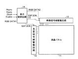
上記入力制御回路15は、表示制御回路14に入力された入力信号を、TG16又は映像信号線駆動回路12に送信する制御を行う。該入力制御回路15には、入力信号としての、垂直同期信号Vsync、水平同期信号Hsync、クロック信号Clock、書込み許可信号Enable、RGBのデータ信号DATA1(入力データ)が入力される。上記入力制御回路15は、これらの入力信号のうち、データ信号DATA1を、データ信号DATA2(画像データ)として、映像信号線駆動回路12に出力し、水平同期信号Hsync、垂直同期信号Vsync、クロック信号Clock、書込み許可信号EnableをTG16に送信する。
The
上記TG16は、映像信号線駆動回路12及び走査信号線駆動回路13に入力される駆動信号を生成する。上記TG16は、図4に示すように、該TG16に入力されたクロック信号Clockをカウントするカウンタ回路4と、該TG16にて生成される駆動信号の立ち上がり及び立ち下がりのタイミングをそれぞれ決定する一致回路5a・5bと、該一致回路5a・5bで検出された立ち上がり及び立ち下がりに基づいて、駆動信号を波形として出力するJKフリップフロップ回路6とを備えている。なお、図4中には、2つの一致回路5a・5bを示しているが、実際には、生成される駆動信号のそれぞれについて、立ち上がり及び立ち下がりを決定するため、生成される駆動信号の2倍の数の一致回路が設けられている。
The TG 16 generates drive signals that are input to the video signal
これらの構成によって、上記TG16は、入力信号に基づいて、ソーススタート信号SSP、ソースクロック信号SCK、ラッチ信号LS、ゲートスタート信号GSP、ゲートクロック信号GCKを生成する。そして、ソーススタート信号SSP、ソースクロック信号SCK、ラッチ信号LSを、映像信号駆動回路12に出力し、ゲートスタート信号GSP、ゲートクロック信号GCKを走査信号線駆動回路13に出力する。
With these configurations, the TG 16 generates a source start signal SSP, a source clock signal SCK, a latch signal LS, a gate start signal GSP, and a gate clock signal GCK based on an input signal. Then, the source start signal SSP, the source clock signal SCK, and the latch signal LS are output to the video
一方、上記入力信号のうちのデータ信号DATA1は、入力制御回路15から、RGBのデータ信号DATA2として、映像信号駆動回路12に出力される。なお、該データ信号DATA2、及び、上記したソーススタート信号SSP、ソースクロック信号SCK、ラッチ信号LS、ゲートスタート信号GSP、ゲートクロック信号GCKは、いずれも、上記液晶パネル11を駆動するための駆動信号である。
On the other hand, the data signal DATA1 among the input signals is output from the
次に、上記構成の液晶表示装置の駆動方法について、説明する。上記構成の液晶表示装置で行われる各液晶セルへの映像信号の書込みは、一般に、交流駆動によって行われる。例えば、ライン反転方式で交流駆動する際には、画素電極に印加される映像信号の極性が、走査信号線毎に反転するように駆動される。交流駆動によって液晶表示装置を駆動する場合、液晶に印加される電圧の実効値は、画素電極に印加される電圧と、対向電極に印加される電圧Vcomとの差によって決定される。そのため、ライン反転方式で液晶表示装置を駆動する際には、各画素電極に印加される電圧の極性が反転した場合にも、液晶に印加される電圧の実効値が等しくなるように、対向電極に電圧Vcomが印加される。それゆえ、画素電極に印加される電圧の極性(映像信号の極性)の反転に合わせて、対向電極の電圧Vcomの極性も反転させる必要がある。 Next, a driving method of the liquid crystal display device having the above configuration will be described. In general, the writing of the video signal to each liquid crystal cell performed in the liquid crystal display device having the above configuration is performed by AC driving. For example, when AC driving is performed by the line inversion method, the polarity of the video signal applied to the pixel electrode is driven so as to be inverted for each scanning signal line. When the liquid crystal display device is driven by AC driving, the effective value of the voltage applied to the liquid crystal is determined by the difference between the voltage applied to the pixel electrode and the voltage Vcom applied to the counter electrode. Therefore, when driving the liquid crystal display device by the line inversion method, even if the polarity of the voltage applied to each pixel electrode is reversed, the counter electrode is set so that the effective value of the voltage applied to the liquid crystal becomes equal. Is applied with a voltage Vcom. Therefore, it is necessary to invert the polarity of the voltage Vcom of the counter electrode in accordance with the inversion of the polarity of the voltage applied to the pixel electrode (the polarity of the video signal).
上記対向電極の電圧Vcomの極性を反転させる駆動を行うと、該対向電極が設けられているガラス基板が、対向電極への電圧の印加によって振動する。このガラス基板の振動の周波数が人間の可聴帯域内である場合、該振動は、液晶表示装置の駆動時に音鳴り(雑音)として知覚されることになる。 When driving to invert the polarity of the voltage Vcom of the counter electrode is performed, the glass substrate provided with the counter electrode vibrates by application of the voltage to the counter electrode. When the frequency of the vibration of the glass substrate is within the human audible band, the vibration is perceived as a sound (noise) when the liquid crystal display device is driven.
そこで、本参考の形態では、液晶表示装置の駆動による音鳴りの発生を防止するために、上記対向電極の電圧Vcomの極性を反転させる対向電極の駆動周波数を、人間の可聴範囲以上の周波数、すなわち20kHz以上に設定する。一般に、ライン反転方式で液晶表示装置を駆動する場合、1水平(1H)期間毎に、対向電極の電圧Vcomの極性が反転することになる。また、周波数は周期の逆数で表されることから、上記対向電極の駆動周波数f(Hz)は、下式
f(Hz)=1/2H期間
で表される。本参考の形態では、上記駆動周波数fを20kHz(20,000Hz)以上に設定するため、上記式より、
f(Hz)=20,000≧1/2H期間
となり、1H期間は、
1H期間≦1/40,000Hz=25μs
となる。すなわち、本参考の形態では、1H期間を25μ秒以下に設定することにより、対向電極の駆動周波数fを20kHz以上にすることができる。
Therefore, in this reference embodiment, in order to prevent the occurrence of audible noise caused by the driving of the liquid crystal display device, the driving frequency of the counter electrode to invert the polarity of the voltage Vcom of the counter electrode, human audible range of frequencies, That is, it is set to 20 kHz or more. In general, when a liquid crystal display device is driven by a line inversion method, the polarity of the voltage Vcom of the counter electrode is inverted every horizontal (1H) period. Further, since the frequency is represented by the reciprocal of the period, the driving frequency f (Hz) of the counter electrode is represented by the following formula f (Hz) = 1 / 2H period. In this reference embodiment, in order to set the drive frequency f to 20 kHz (20,000 Hz) or more, the above equation,
f (Hz) = 20,000 ≧ 1 / 2H period, and 1H period is
1H period ≦ 1 / 40,000Hz = 25μs
It becomes. That is, in this reference embodiment, by setting the 1H period below 25μ seconds, the driving frequency f of the counter electrode can be at least 20 kHz.
ところで、対向電極の駆動周波数を、上記のように20kHz以上にすると、通常よりも、液晶表示装置が高速で駆動することになるため、駆動に要する消費電力が大幅に増加する。一方、例えば、現在の携帯電話等に用いられているQVGA(240×320dot)の解像度を有する液晶パネル11にて、1H期間を25μsとすれば、1フレーム分の液晶セルに電圧を印加するために必要な期間は、走査信号線が320line(ライン)であることから、
25μs×320line=8ms
となる。
By the way, when the drive frequency of the counter electrode is set to 20 kHz or more as described above, the liquid crystal display device is driven at a higher speed than usual, so that the power consumption required for driving is greatly increased. On the other hand, for example, in a
25 μs × 320 line = 8 ms
It becomes.
一般的な液晶表示装置では、1フレーム分を表示するために必要な期間である1垂直(以下、1V)期間(1フレーム期間)は、1/60s(約16.7ms)である。このことから、対向電極の駆動周波数を20kHz以上に設定すると、1フレーム分の1V期間(約16.7ms)の約半分の期間(8ms)で、1フレーム分の液晶セルに電圧を印加することが可能になる。 In a general liquid crystal display device, one vertical (hereinafter, 1 V) period (one frame period), which is a period necessary for displaying one frame, is 1/60 s (about 16.7 ms). For this reason, when the driving frequency of the counter electrode is set to 20 kHz or higher, a voltage is applied to the liquid crystal cells for one frame in about half the period (8 ms) of 1 V period (about 16.7 ms) for one frame. Is possible.
そこで、本参考の形態では、1フレーム分の映像信号の書込みを行った後、映像信号の書込みを行わない期間を設けている。つまり、1V期間のうちの約半分の期間では、対向電極と画素電極とを駆動して、液晶セルに映像信号の書込みを行い、残りの約半分の期間では、対向電極と画素電極とを駆動しないことによって、電力消費を抑制している。これにより、対向電極の駆動周波数を高周波数化しない場合と同等の消費電力で液晶表示装置を駆動することができるので、対向電極や画素電極の駆動周波数を高周波数化することによる消費電力の増大を防止することができる。 Therefore, in this reference embodiment, after the writing of one frame of the video signal is provided with a period that does not perform writing of the video signal. That is, the counter electrode and the pixel electrode are driven in about half of the 1V period to write the video signal in the liquid crystal cell, and the counter electrode and the pixel electrode are driven in the remaining half period. By not doing so, power consumption is suppressed. As a result, the liquid crystal display device can be driven with the same power consumption as when the counter electrode drive frequency is not increased. Therefore, the power consumption is increased by increasing the drive frequency of the counter electrode and the pixel electrode. Can be prevented.
液晶表示装置にて画像表示を行う場合には、画素電極と対向電極との間で、液晶セル内の液晶に電圧が印加される。そのため、液晶への電圧の印加に際しては、画素電極と対向電極とを同じタイミングで駆動する必要がある。従って、上記したように、対向電極を駆動して映像信号の書込みを行う期間(以下、駆動期間)と、対向電極を駆動せず、映像信号の書込みを行わない期間(以下、駆動停止期間)とを設けて、液晶表示装置を駆動するためには、対向電極の駆動のタイミングに合わせて、液晶セルへの映像信号の書込みを行う必要がある。言い換えれば、対向電極の駆動周波数fに基づいて設定される1H期間毎に、データ信号DATA2の極性を反転させて、各液晶セルに該データ信号DATA2の書込みを行う必要がある。 When displaying an image on a liquid crystal display device, a voltage is applied to the liquid crystal in the liquid crystal cell between the pixel electrode and the counter electrode. Therefore, when applying a voltage to the liquid crystal, it is necessary to drive the pixel electrode and the counter electrode at the same timing. Therefore, as described above, a period in which the counter electrode is driven to write the video signal (hereinafter referred to as a driving period), and a period in which the counter electrode is not driven and the video signal is not written (hereinafter referred to as a driving stop period). In order to drive the liquid crystal display device, it is necessary to write a video signal to the liquid crystal cell in accordance with the driving timing of the counter electrode. In other words, it is necessary to invert the polarity of the data signal DATA2 and write the data signal DATA2 to each liquid crystal cell every 1H period set based on the driving frequency f of the counter electrode.
本参考の形態では、対向電極の駆動に合わせてデータ信号DATA2の書込みを行うために、対向電極の駆動周波数fの高周波数化に合わせて、データ信号DATA2の周波数も高周波数化して、各液晶セルへの映像信号の書込みを行っている。この映像信号の書込みのタイミングについて、図1に基づいて説明する。図1は、本発明の液晶表示装置における1V期間の駆動タイミングを表す駆動波形の波形図である。 In this reference embodiment, in order to write the data signal DATA2 in accordance with the driving of the counter electrode, in accordance with the higher frequency of the driving frequency f of the counter electrode, the frequency of the data signal DATA2 be higher frequency, the liquid crystal The video signal is written to the cell. The video signal writing timing will be described with reference to FIG. FIG. 1 is a waveform diagram of drive waveforms representing drive timing in a 1V period in the liquid crystal display device of the present invention.
まず、上記構成の液晶表示装置での画像表示に際しては、図3に示す表示制御回路14に、入力信号としての、水平同期信号Hsync、垂直同期信号Vsync、クロック信号Clock、書込み許可信号Enable、RGBのデータ信号DATA1が入力される。上記の各入力信号は、図1に示すタイミングで、表示制御回路14の入力制御回路15に入力される。
First, when an image is displayed on the liquid crystal display device having the above-described configuration, the horizontal synchronizing signal Hsync, the vertical synchronizing signal Vsync, the clock signal Clock, the write permission signal Enable, RGB are input to the
上記したように、本参考の形態では、対向電極の駆動周波数fが所望する周波数となるように、1H期間が設定される。従って、表示制御回路14に入力される水平同期信号Hsync及びデータ信号DATA1は、それぞれ、上記駆動周波数fに基づいて設定される1H期間に同期した波形を有している。また、垂直同期信号Vsyncは、フレーム周波数に同期した波形で、表示制御回路14に入力される。つまり、本参考の形態では、駆動周波数fの高周波数化に対応可能となるように、フレーム周波数を変えずに、各入力信号が高周波数化されている。
As described above, in the present reference embodiment, as the driving frequency f of the counter electrode becomes a desired frequency, 1H period is set. Accordingly, the horizontal synchronization signal Hsync and the data signal DATA1 input to the
上記表示制御回路14の入力制御回路15に入力された入力信号のうち、水平同期信号Hsync、垂直同期信号Vsync、クロック信号Clock、書込み許可信号Enableは、TG16に送られる。該TG16では、これらの信号に基づいて、ソーススタート信号SSP、ソースクロック信号SCK、ラッチ信号LS、ゲートスタート信号GSP、ゲートクロック信号GCKを生成する。
Of the input signals input to the
具体的には、入力制御回路15に入力されたクロック信号Clockを利用して、垂直同期信号の立ち下がりを取り込む。続いて、図4に示すカウンタ回路4が、クロック信号Clockのカウントを開始する。カウンタ回路4は、上記水平同期信号Hsyncの立ち下がりでカウントをリセットすることにより、一致回路5a・5bが、ソーススタート信号SSP、ソースクロック信号SCK、ラッチ信号LS、ゲートスタート信号GSP、ゲートクロック信号GCKの各駆動信号のそれぞれの立ち上がり及び立ち下がりのタイミングを決定する。ここで決定されたタイミングに基づいて、JKフリップフロップ回路6にて、ソーススタート信号SSP、ソースクロック信号SCK、ラッチ信号LS、ゲートスタート信号GSP、ゲートクロック信号GCKの波形を生成する(図1)。
Specifically, the falling edge of the vertical synchronizing signal is captured using the clock signal Clock input to the
このように、本参考の形態では、入力されたクロック信号Clock及び水平同期信号Hsyncに基づいて、各駆動信号が生成されるので、これらの駆動信号は、水平同期信号Hsyncに同期した周期で生成されることになる。上記したように、水平同期信号Hsyncは、対向電極の駆動周波数に合わせて、高周波数化されている。そのため、TG16で生成される上記の各駆動信号も高周波数化される。 Thus, in this reference embodiment, based on the input clock signal Clock and the horizontal synchronizing signal Hsync, since the drive signal is generated, these drive signals generated at a cycle synchronized with the horizontal synchronizing signal Hsync Will be. As described above, the horizontal synchronization signal Hsync is increased in frequency in accordance with the driving frequency of the counter electrode. Therefore, each drive signal generated by the TG 16 is also increased in frequency.
このようにして、上記TG16で生成されたソーススタート信号SSP、ソースクロック信号SCK、ラッチ信号LSは、映像信号駆動回路12に出力され、TG16で生成されたゲートスタート信号GSP、ゲートクロック信号GCKは、走査信号線駆動回路13に出力される。
In this way, the source start signal SSP, the source clock signal SCK, and the latch signal LS generated by the TG 16 are output to the video
一方、上記表示制御回路14の入力制御回路15に入力された入力信号のうち、データ信号DATA1は、RGBのデータ信号DATA2として、入力制御回路15から映像信号駆動回路12(図2)に出力される。すなわち、入力されたクロック信号Clockを利用して、垂直同期信号の立ち下がりを取り込む。そして、入力制御回路15にて、上記クロック信号Clockをカウントし、水平同期信号Hsyncの立ち下がりでカウントをリセットする。これにより、入力されたデータ信号DATA1を出力するタイミング、つまり、データ信号DATA2の立ち上がり及び立ち下がりのタイミングが決定されて、入力制御回路15から、データ信号DATA2が映像信号線駆動回路12に出力される(図1)。
On the other hand, among the input signals input to the
このようにして、各駆動信号が映像信号駆動回路12及び走査信号線駆動回路13に出力されると、上記映像信号線駆動回路12は、図1に示すように、表示制御回路14から入力されたソーススタート信号SSPを基準として、ソースクロック信号SCKに従って、データ信号DATA2をサンプリングする。そして、映像信号線駆動回路12が1H期間分のデータ信号DATA2をサンプリングすると、ラッチ信号LSの入力によって、サンプリングされたデータ信号DATA2に対応する液晶駆動用電圧を、液晶パネル11の映像信号線に出力する。
Thus, when each drive signal is output to the video
一方、上記走査信号線駆動回路13は、図1に示すように、1V期間に、ゲートスタート信号GSPを1回出力する。また、上記走査信号線駆動回路13は、1H期間毎に、ゲートクロック信号GCKを出力する。
On the other hand, as shown in FIG. 1, the scanning signal
上記走査信号線駆動回路13が、ゲートスタート信号GSP及びゲートクロック信号GCKを受け取ると、TFTをオンとするための電圧を走査信号線に出力する。これにより、走査信号線上のTFTがオン状態となり、映像信号線から伝達されるデータ信号DATA2の電圧が、液晶セルに充電される。その後、同様の動作により、映像信号線駆動回路12に対する二番目の走査信号線に、該二番目の走査信号線上のTFTをオンとするための電圧が出力され、TFTがオンとなるタイミングで、上記一番目の走査信号線上のTFTがオフ状態となり、液晶セルに充電された電圧を保持する。
When the scanning signal
上記のように、上記走査信号線駆動回路13は、上記表示制御回路14からのゲートスタート信号GSPやゲートクロック信号GCK等のタイミング信号に同期して、各走査信号線を順次、選択しながら走査し、TFTのオン/オフを制御する。このようにして、一つの映像信号線に交差する全ての走査信号線上のTFTへの電圧の充電・保持により、1フレーム分のデータ信号DATA2の書込みが完了して、液晶パネル11には、画像が表示される。
As described above, the scanning signal
上記したように、例えば、QVGA(240×320dot)の解像度を有する液晶パネル11にて、1H期間を25μsとすれば、1フレーム分のデータ信号DATA2の書込みは、8msで終了する。一般的な液晶表示装置では、1V期間は約16.7msである。そのため、本参考の形態では、図1に示すように、データ信号DATA2の書込みを行った後、次の1V期間(次の映像信号線へのデータ信号DATA2の出力)が始まるまでの間、データ信号DATA2の書込みを停止するとともに、対向電極の駆動を停止する。その後、垂直同期信号Vsyncが取り込まれるタイミングで、再び、映像信号線駆動回路12へのデータ信号DATA2の出力を開始する。
As described above, for example, when the 1H period is set to 25 μs in the
このように、本参考の形態では、対向電極の駆動周波数を、人間の可聴帯域よりも高い周波数となるように高周波数化するとともに、表示制御回路14に入力される水平同期信号Hsync及びデータ信号DATA1を高周波数化している。それゆえ、液晶表示装置の駆動に際して、対向電極の駆動に伴って生じる振動の周波数を、人間の可聴帯域よりも高くすることができるので、該振動を液晶表示装置の音鳴りとして知覚することはない。
Thus, in the present reference embodiment, the drive frequency of the counter electrode, as well as higher frequency such that the frequency higher than the human audible range, a horizontal synchronization signal Hsync and the data signal inputted to the
また、水平同期信号Hsync及びデータ信号DATA1を高周波数化することにより、液晶セルへのデータ信号DATA2の印加期間は短くなる。対向電極の駆動は、データ信号DATA2を印加するタイミングに合わせて行えばよいので、1V期間のうち、データ信号DATA2が印加されない期間(画素電極が駆動されない期間)については、対向電極を駆動する必要はない。従って、画素電極及び駆動電極の駆動に要する電力量が増大することはない。 Further, by increasing the frequency of the horizontal synchronization signal Hsync and the data signal DATA1, the application period of the data signal DATA2 to the liquid crystal cell is shortened. Since the counter electrode may be driven in accordance with the application timing of the data signal DATA2, it is necessary to drive the counter electrode during a period in which the data signal DATA2 is not applied (period in which the pixel electrode is not driven) in the 1V period. There is no. Accordingly, the amount of power required for driving the pixel electrode and the drive electrode does not increase.
なお、本参考の形態では、対向電極の駆動周波数fを20kHzとする場合を例に挙げて説明したが、20kHzを超える周波数に設定し、1H期間をより一層短く設定してもよい。しかしながら、液晶セル内の液晶を十分に充電するためには、アンプ等の液晶表示装置の構成部材の高性能化が要求されるため、液晶表示装置に備えられている構成部材の性能にて、良好に液晶セルの充電を行い得るように、対向電極の駆動周波数を設定することが望ましい。 In the present reference embodiment, the case where the driving frequency f of the counter electrode and 20kHz has been described as an example, and set to a frequency of greater than 20kHz, may be set more shorter 1H period. However, in order to fully charge the liquid crystal in the liquid crystal cell, high performance of the constituent members of the liquid crystal display device such as an amplifier is required, so the performance of the constituent members provided in the liquid crystal display device is It is desirable to set the driving frequency of the counter electrode so that the liquid crystal cell can be charged satisfactorily.
また、対向電極の駆動周波数は、一般に、液晶表示装置を駆動する際のフレーム周波数(1本の映像信号線に交差する全ての走査信号線を走査する期間)、及び、液晶表示装置の解像度に依存する。従って、フレーム周波数が60Hzであって、走査信号線が666本以上となる場合には、図5に示すように、1V期間を全て駆動期間としても、対向電極の駆動周波数は、20kHz以上に設定されることになる。従って、走査信号線が666本以上となる場合には、図1に示すように、1V期間内に駆動期間と駆動停止期間とを設ける必要はない。 Further, the driving frequency of the counter electrode generally depends on the frame frequency when driving the liquid crystal display device (a period during which all scanning signal lines crossing one video signal line) and the resolution of the liquid crystal display device. Dependent. Therefore, when the frame frequency is 60 Hz and the number of scanning signal lines is 666 or more, as shown in FIG. 5, the driving frequency of the counter electrode is set to 20 kHz or more even if the 1 V period is the driving period. Will be. Therefore, when there are 666 or more scanning signal lines, it is not necessary to provide a driving period and a driving stop period within the 1V period as shown in FIG.
〔実施の形態1〕
本発明の実施の形態について図6ないし図8に基づいて説明すれば、以下の通りである。なお、説明の便宜上、前記の参考の形態の図面に示した部材と同一の機能を有する部材については、同一の符号を付し、その説明を省略する。
[Embodiment 1 ]
If described with reference to FIGS. 6-8 for the implementation of the embodiment of the present invention is as follows. For convenience of explanation, members having the same functions as those shown in the drawings of the above-described reference embodiment are given the same reference numerals, and descriptions thereof are omitted.
本実施の形態の液晶表示装置は、前記参考の形態で説明した液晶表示装置の表示制御回路14(図3)に代えて、図6に示す表示制御回路24を備えている。図6は、本実施の形態の液晶表示装置に備えられた表示制御回路24の構成を示すブロック図である。
The liquid crystal display device of this embodiment includes a
上記表示制御回路24は、図6に示すように、画素電極を駆動するための駆動信号の生成等を行うために、入力制御回路25、TG(タイミングジェネレータ(timing generator))26、メモリ制御回路27、第1表示メモリ(記憶部・第1の記憶部)28、第2表示メモリ(記憶部・第2の記憶部)29を備えている。
As shown in FIG. 6, the
上記入力制御回路25は、表示制御回路24に入力された入力信号を、TG26又は第1表示メモリ28に送信する制御を行う。該入力制御回路25には、入力信号としての、水平同期信号Hsync、垂直同期信号Vsync、クロック信号Clock、書込み許可信号Enable、RGBのデータ信号DATA1が入力される。上記入力制御回路25は、これらの入力信号のうち、データ信号DATA1を第1表示メモリ28に送信し、水平同期信号Hsync、垂直同期信号Vsync、クロック信号Clock、書込み許可信号EnableをTG26に送信する。
The
上記TG26は、第1表示メモリ28、映像信号線駆動回路12、走査信号線駆動回路13に入力される信号を生成する。上記TG26は、図7に示すように、対向電極の駆動周波数に合わせて高周波数化されたクロック信号である内部クロック信号を生成する内部発振回路20と、該内部クロック信号をカウントするカウンタ回路21と、該TG16にて生成される駆動信号の立ち上がり及び立ち下がりのタイミングを決定する一致回路22a・22bと、該一致回路22a・22bで検出された立ち上がり及び立ち下がりに基づいて、駆動信号を波形として出力するJKフリップフロップ回路23とを備えている。なお、図7中には、2つの一致回路22a・22bを示しているが、実際には、生成される駆動信号のそれぞれについて、立ち上がり及び立ち下がりを決定するため、生成される駆動信号の2倍の数の一致回路が設けられている。
The
これらの構成を備えることによって、上記TG26は、入力信号に基づいて、ソーススタート信号SSP、ソースクロック信号SCK、ラッチ信号LS、ゲートスタート信号GSP、ゲートクロック信号GCKを生成する。そして、上記TG26は、生成した駆動信号をメモリ制御回路27に出力するとともに、これらの駆動信号のうち、ソーススタート信号SSP、ソースクロック信号SCK、ラッチ信号LSを、映像信号駆動回路12に出力し、ゲートスタート信号GSP、ゲートクロック信号GCKを走査信号線駆動回路13に出力する。
With these configurations, the
なお、入力制御回路25からTG26に入力された入力信号は、TG26を経てメモリ制御回路27に送信される。また、TG26から第1表示メモリ28には、書込み許可信号Enableが「High」である期間に、クロック信号Clockが出力される。これにより、入力されるデータ信号DATA1に同期して、該データ信号DATA1が格納される。
An input signal input from the
上記メモリ制御回路27は、第1表示メモリ28及び第2表示メモリ29へのデータ信号DATA1の格納や、第1表示メモリ28及び第2表示メモリ29からのデータ信号DATA1・DATA2の読出しを制御する。
The
上記第1表示メモリ28は、例えばRAMであり、入力制御回路25から送信されるデータ信号DATA1を格納し、格納したデータ信号DATA1を第2表示メモリ29に送信する。また、上記第2表示メモリ29は、例えばRAMであり、第1表示メモリ28から送信されたデータ信号DATA1を格納し、格納されたデータ信号DATA1を所定のタイミングで読出して、データ信号DATA2として、映像信号線駆動回路12に出力する。
The
上記構成の表示制御回路24を備えた液晶表示装置にて、前記参考の形態で説明したように駆動期間と駆動停止期間とを設けて行われる各液晶セルへ映像信号の書込みは、図8に示すタイミングで行われる。図8は、本発明の液晶表示装置における駆動タイミングを表す駆動波形の波形図である。
In the liquid crystal display device having the
すなわち、図6に示す表示制御回路24の入力制御回路25に、入力信号としての、水平同期信号Hsync、垂直同期信号Vsync、クロック信号Clock、書込み許可信号Enable、RGBのデータ信号DATA1が入力される。このとき入力される上記入力信号は、前記参考の形態とは異なり、高周波数化されていない。つまり、本実施の形態にて、表示制御回路24に入力される入力信号は、液晶表示装置の音鳴りを防止するために、高周波数化された対向電極の駆動周波数のタイミングに合わせて高周波数化されていない。従って、前記参考の形態にて説明した各液晶セルにデータ信号DATA2を書込むタイミングとは異なった周波数を有している。
That is, the horizontal synchronization signal Hsync, the vertical synchronization signal Vsync, the clock signal Clock, the write enable signal Enable, and the RGB data signal DATA1 are input to the
そのため、本実施の形態では、対向電極の駆動周波数に合わせて、各液晶セルにデータ信号DATA2の書込みが行われるように、高周波数化された駆動信号(ソーススタート信号SSP、ソースクロック信号SCK、ラッチ信号LS、ゲートスタート信号GSP、ゲートクロック信号GCK、データ信号DATA2)を生成する。 Therefore, in the present embodiment, the driving signals (source start signal SSP, source clock signal SCK, source clock signal SCK, high frequency) are written so that the data signal DATA2 is written to each liquid crystal cell in accordance with the driving frequency of the counter electrode. A latch signal LS, a gate start signal GSP, a gate clock signal GCK, and a data signal DATA2).
つまり、入力制御回路25に入力された入力信号のうち、水平同期信号Hsync、垂直同期信号Vsync、クロック信号Clock、書込み許可信号Enableが、TG26に入力されると、該TG26にて、次のようにして、ソーススタート信号SSP、ソースクロック信号SCK、ラッチ信号LS、ゲートスタート信号GSP、ゲートクロック信号GCKを生成する。
That is, when the horizontal synchronization signal Hsync, the vertical synchronization signal Vsync, the clock signal Clock, and the write enable signal Enable are input to the
すなわち、まず、図7に示すTG26に設けられている内部発振回路20で生成される内部クロック信号を利用して、垂直同期信号Vsyncの立ち下がりを取り込む。ここで、上記内部クロック信号は、高周波数化された駆動信号を得るために、前記参考の形態にて、垂直同期信号Vsyncの立ち下がりを取り込むために用いられたクロック信号(図1中、Clock)よりも高い周波数を有している。具体的には、例えば、表示制御回路24に入力されるクロック信号Clockの周波数の約2倍の周波数の内部クロック信号を生成する。
That is, first, the falling edge of the vertical synchronization signal Vsync is captured using the internal clock signal generated by the
続いて、カウンタ回路21が、内部クロック信号のカウントを開始する。このとき、入力信号の周波数よりも高い周波数の駆動信号を得るために、上記カウンタ回路21は、対向電極の電圧Vcomが反転する時間毎に、カウンタをリセットする。対向電極の電圧Vcomが反転する時間は、前記参考の形態にて説明したように、対向電極の駆動周波数fによって算出することができる。これにより、一致回路22a・22bが、ソーススタート信号SSP、ソースクロック信号SCK、ラッチ信号LS、ゲートスタート信号GSP、ゲートクロック信号GCKの各駆動信号のそれぞれの立ち上がり及び立ち下がりのタイミングを決定する。ここで決定されたタイミングに基づいて、JKフリップフロップ回路23にて、ソーススタート信号SSP、ソースクロック信号SCK、ラッチ信号LS、ゲートスタート信号GSP、ゲートクロック信号GCKの波形が生成される。
Subsequently, the
このように、高周波数化された内部クロック信号及び対向電極の駆動周波数fに基づいて各駆動信号を生成することにより、図8に示すように、高周波数化された駆動信号を得ることができる。つまり、本実施の形態では、前記参考の形態とは異なり、表示制御回路24に入力されたクロック信号Clock及び水平同期信号Hsyncは、対向電極の駆動周波数に合わせて高周波数化されていない。そのため、カウンタ回路21が、上記クロック信号Clockをカウントし、水平同期信号Hsyncに基づいてカウントをリセットしても、TG26にて生成される駆動信号を高周波数化することはできない。
In this way, by generating each drive signal based on the internal clock signal having a higher frequency and the drive frequency f of the counter electrode, a drive signal having a higher frequency can be obtained as shown in FIG. . That is, in the present embodiment, unlike the reference embodiment , the clock signal Clock and the horizontal synchronization signal Hsync input to the
そこで、本実施の形態では、上記のように、TG26に内部発振回路20を設け、該内部発振回路20にて、対向電極の駆動周波数に合わせて高周波数化された内部クロック信号を生成している。さらに、対向電極の駆動周波数から算出される電圧Vcomが反転する時間に基づいて、駆動信号の立ち上がり及び立ち下がりのタイミングを決定している。これにより、TG26にて、駆動信号は、高周波数化されて生成されるとともに、駆動信号は、対向電極及び画素電極が駆動する駆動期間に出力され、対向電極及び画素電極が駆動しない駆動停止期間には、出力を停止するような波形で生成される。
Therefore, in the present embodiment, as described above, the
このようにして生成された駆動信号のうち、ソーススタート信号SSP、ソースクロック信号SCK、ラッチ信号LSは、映像信号駆動回路12に出力され、ゲートスタート信号GSP、ゲートクロック信号GCKは、走査信号線駆動回路13に出力される。
Of the drive signals thus generated, the source start signal SSP, the source clock signal SCK, and the latch signal LS are output to the video
一方、表示制御回路24に入力された入力信号のうち、データ信号DATA1は、図8に示すように、駆動期間だけでなく駆動停止期間にも入力される。しかしながら、本実施の形態では、1V期間に、駆動期間と駆動停止期間とが設けられているので、表示制御回路24にデータ信号DATA1が入力されるタイミングで、表示制御回路24から映像信号線駆動回路12にデータ信号DATA2を送信しても、対向電極が駆動していなければ、液晶セルを充電することはできない。
On the other hand, among the input signals input to the
そこで、入力されたデータ信号DATA1を、入力制御回路25から第1表示メモリ28に送信し、一時的に、第1表示メモリ28に蓄積する。そして、第1表示メモリ28に格納されたデータ信号DATA1を、メモリ制御回路27の制御によって所定のタイミングで、第2表示メモリ29に送信し、該第2表示メモリ29に格納する。その後、次の1V期間に、第2表示メモリ29から、RGBのデータ信号DATA2として、映像信号駆動回路12に出力する。つまり、本実施の形態では、データ信号DATA1が入力される1V期間に続く次の1V期間(図8)に、データ信号DATA2が出力される。従って、データ信号DATA1の入力と、データ信号DATA2の出力との間には、1V期間程度の遅れが生じることになる。
Therefore, the input data signal DATA1 is transmitted from the
ここで、第1表示メモリ28から第2表示メモリ29にデータ信号DATA1を送信する所定のタイミングは、1V期間(1フレーム)分のデータ信号DATA1が全て、第1表示メモリ28に格納された後であれば特に限定されない。ただし、液晶パネル11に表示される画像の遅延を回避するためには、次の1V期間のうちの早い段階に、データ信号DATA2の書込みを行うことが好ましい。そのため、データ信号DATA1が入力される1V期間内に、第1表示メモリ28から第2表示メモリ29へのデータ信号DATA1の転送を行うことが好ましい。
Here, the predetermined timing for transmitting the data signal DATA1 from the
上記第1・第2表示メモリ28・29間でのデータ信号DATA1の転送が完了すると、メモリ制御回路27が、垂直同期信号Vsyncの立ち下がりのタイミングで、TG26内の内部発振回路20にて生成される内部クロック信号のカウントを開始する。続いて、上記メモリ制御回路27は、対向電極の電圧Vcomが反転する時間毎に、内部クロック信号のカウントをリセットする。これにより、入力されたデータ信号DATA1を出力するタイミング、つまり、データ信号DATA2の立ち上がり及び立ち下がりのタイミングが決定されて、上記メモリ制御回路27の制御により、図8に示すように、データ信号DATA2が映像信号線駆動回路12に出力される。このようにして出力される上記データ信号DATA2は、高周波数化された内部クロック信号及び対向電極の駆動周波数fに基づいて、第2表示メモリ29から出力されるため、図8に示すように、高周波数となっている。
When the transfer of the data signal DATA1 between the first and
その後、上記表示制御部24から、映像信号駆動回路12及び走査信号線駆動回路13に駆動信号が出力されると、前記参考の形態にて説明したように、液晶セルの充電、電圧の保持が行われて、液晶パネル11に画像が表示される。
After that, when the drive signal is output from the
このように、本実施の形態では、表示制御部24内のTG26に内部発振回路20を設けて高周波数の内部クロック信号を生成し、該内部クロック信号と、対向電極の駆動周波数とに基づいて、駆動信号を生成している。これにより、対向電極の駆動周波数とは異なるタイミングを有する入力信号が入力された場合にも、対向電極の駆動周波数に合わせたタイミングの駆動信号を生成し、図8に示すように、1V期間に駆動期間と駆動停止期間とを設けて、液晶表示装置を駆動することができる。それゆえ、1V期間のうちの駆動期間には、人間の可聴帯域よりも高い周波数で対向電極を駆動して、液晶パネル11を駆動して音鳴りを防止することができる。また、高周波数で液晶表示装置を駆動することによって増大する消費電力を相殺するために、1V期間内に、電力がほとんど消費されない駆動停止期間を設けているので、液晶表示装置全体としての消費電力の増大を回避することができる。
As described above, in this embodiment, the
なお、本実施の形態で用いられる第1表示メモリ28及び第2表示メモリ29の容量は、液晶パネル11の解像度、データ信号DATA1の入力、データ信号DATA2の出力等を考慮して決定すればよい。本実施の形態では、1V期間に入力されるデータ信号を一旦、各メモリに格納するので、例えば、1V期間に表示される画像のデータに相当する容量以上の容量を有していればよい。各メモリの容量が少ないほど、液晶表示装置の小型化を実現して、コストを削減することができる。
The capacities of the
〔実施の形態2〕
本発明の他の実施の形態について図9ないし図10に基づいて説明すれば、以下の通りである。なお、説明の便宜上、前記の参考の形態および実施の形態1の図面に示した部材と同一の機能を有する部材については、同一の符号を付し、その説明を省略する。
[Embodiment 2 ]
The following will describe another embodiment of the present invention with reference to FIGS. For convenience of explanation, members having the same functions as those shown in the drawings of the reference embodiment and the first embodiment are given the same reference numerals, and explanation thereof is omitted.
本実施の形態の液晶表示装置は、前記実施の形態1で説明した液晶表示装置の表示制御回路24(図6)に代えて、図9に示す表示制御回路34を備えている。図9は、本実施の形態の液晶表示装置に備えられた表示制御回路34の構成を示すブロック図である。
The liquid crystal display device of the present embodiment includes a
上記表示制御回路34は、図9に示すように、画素電極を駆動するための駆動信号の生成等を行うために、入力制御回路35、TG(タイミングジェネレータ(timing generator))36、メモリ制御回路37、表示メモリ(記憶部)38を備えている。
As shown in FIG. 9, the
上記入力制御回路35は、表示制御回路34に入力された入力信号を、TG36又は表示メモリ38に送信する制御を行う。該入力制御回路35には、入力信号としての、水平同期信号Hsync、垂直同期信号Vsync、クロック信号Clock、書込み許可信号Enable、RGBのデータ信号DATA1が入力される。上記入力制御回路35は、これらの入力信号のうち、データ信号DATA1を表示メモリ38に送信し、水平同期信号Hsync、垂直同期信号Vsync、クロック信号Clock、書込み許可信号EnableをTG36に送信する。
The
上記TG36は、表示メモリ38、映像信号線駆動回路12、走査信号線駆動回路13に入力される信号を生成する。上記TG36の詳細な構成は、前記実施の形態1で説明した図7に示すTG26と同じであるので、ここでは説明を省略する。なお、TG36にて生成された駆動信号は、前記実施の形態1で説明したように、映像信号駆動回路12及び走査信号線駆動回路13に出力されるとともに、表示メモリ38及びメモリ制御回路37に出力される。
The
なお、入力制御回路35からTG36に入力された入力信号は、TG36を経てメモリ制御回路37に送信される。また、TG36から表示メモリ38には、書込み許可信号Enableが「High」である期間に、クロック信号Clockが出力される。これにより、入力されるデータ信号DATA1に同期して、該データ信号DATA1が表示メモリ38に格納される。
The input signal input from the
上記メモリ制御回路37は、表示メモリ38へのデータ信号DATA1の格納、データ信号DATA2の読出しを制御する。
The memory control circuit 37 controls the storage of the data signal DATA1 in the
上記表示メモリ38は、入力制御回路35から送信されるデータ信号DATA1を格納し、該データ信号DATA1を所定のタイミングで、データ信号DATA2として読み出して、映像信号線駆動回路12に出力する。
The
上記構成の表示制御回路34を備えた液晶表示装置にて、駆動期間と駆動停止期間とを設けて行われる各液晶セルへ映像信号の書込みは、図10に示すタイミングで行われる。図10は、本発明の液晶表示装置における1V期間の駆動タイミングを表す駆動波形の波形図である。
In the liquid crystal display device having the
すなわち、図6に示す表示制御回路24の入力制御回路25に、入力信号としての、水平同期信号Hsync、垂直同期信号Vsync、クロック信号Clock、書込み許可信号Enable、RGBのデータ信号DATA1が入力される。このとき入力される上記入力信号は、前記参考の形態のように高周波数化されていない。つまり、本実施の形態にて、表示制御回路24に入力される入力信号は、液晶表示装置の音鳴りを防止するために、高周波数化された対向電極の駆動周波数のタイミングに合わせて高周波数化されていない。
That is, the horizontal synchronization signal Hsync, the vertical synchronization signal Vsync, the clock signal Clock, the write enable signal Enable, and the RGB data signal DATA1 are input to the
そのため、本実施の形態では、前記実施の形態1と同様に、対向電極の駆動周波数に合わせて、各液晶セルにデータ信号DATA2の書込みが行われるように、高周波数化された駆動信号(ソーススタート信号SSP、ソースクロック信号SCK、ラッチ信号LS、ゲートスタート信号GSP、ゲートクロック信号GCK、データ信号DATA2)を生成する。 Therefore, in the present embodiment, similarly to the first embodiment, the driving signal (source) having a higher frequency is written so that the data signal DATA2 is written in each liquid crystal cell in accordance with the driving frequency of the counter electrode. A start signal SSP, a source clock signal SCK, a latch signal LS, a gate start signal GSP, a gate clock signal GCK, and a data signal DATA2).
ここで、TG36では、前記実施の形態1で説明したTG26で行われる駆動信号の生成と同様にして、ソーススタート信号SSP、ソースクロック信号SCK、ラッチ信号LS、ゲートスタート信号GSP、ゲートクロック信号GCKが生成される。
Here, in the
一方、表示制御回路34に入力された入力信号のうち、データ信号DATA1は、入力制御回路35から表示メモリ38に送信され、該表示メモリ38に蓄積される。そして、メモリ制御回路37が、垂直同期信号Vsyncの立ち下がりのタイミングから、水平同期信号Hsyncをカウントし、所定のカウントに達した時点で、表示メモリ38に格納されたデータ信号DATA1を、データ信号DATA2として読出して、映像信号線駆動回路12に出力する。
On the other hand, among the input signals input to the
ここで、表示メモリ38からデータ信号DATA2の出力は、前記実施の形態1と同様に行われる。すなわち、メモリ制御回路37が、TG36内の内部発振回路にて生成された内部クロック信号のカウントを開始する。この内部クロック信号は、前記実施の形態1で説明した内部クロック信号であり、入力信号のクロック信号Clockよりも高い周波数を有している。続いて、上記メモリ制御回路37が、対向電極の電圧Vcomが反転する時間毎に、内部クロック信号のカウントをリセットすることにより、入力されたデータ信号DATA1を出力するタイミング、つまり、データ信号DATA2の立ち上がり及び立ち下がりのタイミングが決定される。このようにして、上記メモリ制御回路37の制御により、図10に示すように、データ信号DATA2が映像信号線駆動回路12に出力される。出力されるデータ信号DATA2は、高周波数化された内部クロック信号及び対向電極の駆動周波数fに基づいて、表示メモリ38から出力されるため、図10に示すように、高周波数となっている。
Here, the output of the data signal DATA2 from the
ところで、本実施の形態では、図10に示すように、上記データ信号DATA2が映像信号線駆動回路12に出力されている間も、表示制御部35にはデータ信号DATA1が入力され、順次、表示メモリ38に格納される。そのため、上記データ信号DATA2の出力中に格納されたデータ信号DATA1も、順次、データ信号DATA2として、映像信号線駆動回路12に出力される。つまり、表示メモリ38では、データ信号DATA1の書込みを行いながら、データ信号DATA2の読出しが行われる。従って、本実施の形態では、前記実施の形態1とは異なり、1V期間に入力されたデータ信号DATA1を、同じ1V期間に、データ信号DATA2として出力することができる。
In the present embodiment, as shown in FIG. 10, while the data signal DATA2 is being output to the video signal
このように、本実施の形態では、上記表示メモリ38は、データ信号DATA1の入力と、データ信号DATA2の出力とを並行して行うため、デュアルゲートのメモリであることが好ましい。これにより、1V期間の初期に記憶されたデータ信号を、順次読出して、データ信号DATA2として出力することができる。
As described above, in the present embodiment, the
以上のようにして、上記表示制御部24から、映像信号駆動回路12及び走査信号線駆動回路13に駆動信号が出力されると、前記参考の形態にて説明したように、液晶セルの充電、電圧の保持が行われて、液晶パネル11に画像が表示される。
As described above, when the driving signal is output from the
なお、本実施の形態の表示メモリ38の容量は、上記したタイミングで、データ信号DATA1の入力と、データ信号DATA2の出力とを並行して行うことができる大きさであればよい。つまり、本実施の形態では、表示メモリ38に格納されたデータ信号DATA1が順次データ信号DATA2として出力されることによって生じた空き容量に、新たなデータ信号DATA1の書込みを行うことができる。従って、前記実施の形態1の第1・第2表示メモリ28・29のように、1V期間に表示される画像のデータに相当する容量以上の容量を有していなくてもよい。
Note that the capacity of the
本発明は上述した各実施形態に限定されるものではなく、請求項に示した範囲で種々の変更が可能であり、異なる実施形態にそれぞれ開示された技術的手段を適宜組み合わせて得られる実施形態についても本発明の技術的範囲に含まれる。 The present invention is not limited to the above-described embodiments, and various modifications are possible within the scope shown in the claims, and embodiments obtained by appropriately combining technical means disclosed in different embodiments. Is also included in the technical scope of the present invention.
本発明の液晶表示装置及びその駆動方法は、携帯電話、デジタルカメラ、パーソナルコンピュータ、液晶テレビ等のディスプレイに対して適用することができる。これにより、消費電力を増大させることなく、音鳴りを防止することができる液晶表示装置を提供することができる。 The liquid crystal display device and the driving method thereof according to the present invention can be applied to displays such as mobile phones, digital cameras, personal computers, and liquid crystal televisions. Thereby, it is possible to provide a liquid crystal display device capable of preventing sound generation without increasing power consumption.
4 カウンタ回路
5a 一致回路
5b 一致回路
6 JKフリップフロップ回路
11 液晶パネル(表示部)
12 映像信号線駆動回路(駆動回路)
13 走査信号線駆動回路
14 表示制御回路
15 入力制御回路
16 TG(タイミングジェネレータ)
20 内部発振回路
21 カウンタ回路
22a 一致回路
22b 一致回路
23 JKフリップフロップ回路
24 表示制御回路
25 入力制御回路
26 TG(タイミングジェネレータ)
27 メモリ制御回路(記憶部制御装置)
28 第1表示メモリ(記憶部)
29 第2表示メモリ(記憶部)
34 表示制御回路
35 入力制御回路
36 TG(タイミングジェネレータ)
37 メモリ制御回路(記憶部制御装置)
38 表示メモリ(記憶部)
Vsync 垂直同期信号
Hsync 水平同期信号
Clock クロック信号
Enable 書込み許可信号
DATA1 データ信号(入力データ)
SSP ソーススタート信号
SCK ソースクロック信号
LS ラッチ信号
GSP ゲートスタート信号
GCK ゲートクロック信号
DATA2 データ信号(出力データ)
4 counter circuit
12 Video signal line drive circuit (drive circuit)
13 Scanning Signal
20
27 Memory control circuit (storage unit control device)
28 First display memory (storage unit)
29 Second display memory (storage unit)
34
37 Memory control circuit (storage unit control device)
38 Display memory (storage unit)
Vsync Vertical synchronization signal Hsync Horizontal synchronization signal Clock Clock signal Enable Write enable signal DATA1 Data signal (input data)
SSP source start signal SCK source clock signal LS latch signal GSP gate start signal GCK gate clock signal DATA2 data signal (output data)
Claims (7)
上記液晶表示装置には、入力データを格納する記憶部を備え、
上記1フレーム期間に、上記対向電極を駆動する駆動期間と、上記対向電極を駆動しない駆動停止期間とを設け、
上記駆動期間には、人間の可聴帯域よりも高い周波数で上記対向電極を駆動するとともに、該対向電極の駆動タイミングに合わせて、上記記憶部から駆動回路に画像データを出力し、
上記駆動停止期間には、上記駆動回路への画像データの出力を停止することを特徴とする液晶表示装置の駆動方法。 In order to display an image on a display unit having a counter electrode arranged so as to face a pixel electrode arranged in a lattice-like region partitioned by a scanning signal line and a video signal line through a liquid crystal layer In addition, in a driving method of an active matrix liquid crystal display device that sequentially displays an image for one frame on the display unit by outputting image data for one frame generated based on input data to a driving circuit,
The liquid crystal display device includes a storage unit for storing input data,
In the one frame period, a driving period for driving the counter electrode and a driving stop period for not driving the counter electrode are provided,
During the drive period, the counter electrode is driven at a frequency higher than the human audible band , and image data is output from the storage unit to the drive circuit in accordance with the drive timing of the counter electrode ,
A driving method of a liquid crystal display device, wherein output of image data to the driving circuit is stopped during the driving stop period.
第1の記憶部に所定量の入力データを格納した後に、該入力データを第2の記憶部に転送し、
上記第2の記憶部に転送された入力データに基づいて生成した画像データを、上記対向電極を駆動する駆動期間に、対向電極の駆動タイミングに合わせて、該第2の記憶部から駆動回路に出力することを特徴とする請求項1記載の液晶表示装置の駆動方法。 The storage unit has at least two storage units,
After storing a predetermined amount of input data in the first storage unit, the input data is transferred to the second storage unit,
The image data generated based on the input data transferred to the second storage unit is transferred from the second storage unit to the drive circuit in accordance with the drive timing of the counter electrode in the drive period for driving the counter electrode. the driving method of the liquid crystal display device according to claim 1, wherein the output.
上記表示制御部は、該表示制御部に入力された入力信号のうち、上記表示部に表示される画像データを格納する記憶部と、
人間の可聴帯域よりも高い周波数で上記対向電極を駆動する駆動タイミングに合わせて、上記記憶部から上記駆動回路に上記画像データを出力するタイミングを制御する記憶部制御装置と、を備えていることを特徴とする液晶表示装置。 Controls image display on a display unit that has a counter electrode that is arranged so as to face the pixel electrode arranged in a grid-like region divided by the scanning signal line and the video signal line through a liquid crystal layer. In the active matrix type liquid crystal display device in which a display control unit generates a drive signal for driving the drive circuit based on an input signal in order to drive the drive circuit
The display control unit includes a storage unit that stores image data displayed on the display unit among input signals input to the display control unit;
A storage unit control device that controls the timing of outputting the image data from the storage unit to the drive circuit in accordance with the drive timing of driving the counter electrode at a frequency higher than a human audible band. A liquid crystal display device.
上記第1の記憶部から転送された所定量の画像データを、上記対向電極の駆動タイミングに合わせて駆動回路に出力する第2の記憶部と、を有していることを特徴とする請求項4記載の液晶表示装置。 The storage unit includes a first storage unit that stores a predetermined amount of image data input to the display control unit;
2. A second storage unit that outputs a predetermined amount of image data transferred from the first storage unit to a drive circuit in accordance with the drive timing of the counter electrode. 4. The liquid crystal display device according to 4 .
Priority Applications (5)
| Application Number | Priority Date | Filing Date | Title |
|---|---|---|---|
| JP2004042014A JP4108623B2 (en) | 2004-02-18 | 2004-02-18 | Liquid crystal display device and driving method thereof |
| KR1020050013076A KR100625702B1 (en) | 2004-02-18 | 2005-02-17 | Liquid crystal display device, driving method, driving device, and display control device |
| US11/059,349 US7999781B2 (en) | 2004-02-18 | 2005-02-17 | Liquid crystal display device, driving device, display control device, and method of driving at a frequency higher than an audible frequency band for a human being having a drive period and drive suspension period |
| TW094104672A TWI286301B (en) | 2004-02-18 | 2005-02-17 | Liquid crystal display device, driving method, driving device, and display control device |
| CNB2005100717439A CN100466053C (en) | 2004-02-18 | 2005-02-18 | Liquid crystal display device, driving method, driving device, and display control device |
Applications Claiming Priority (1)
| Application Number | Priority Date | Filing Date | Title |
|---|---|---|---|
| JP2004042014A JP4108623B2 (en) | 2004-02-18 | 2004-02-18 | Liquid crystal display device and driving method thereof |
Publications (2)
| Publication Number | Publication Date |
|---|---|
| JP2005234139A JP2005234139A (en) | 2005-09-02 |
| JP4108623B2 true JP4108623B2 (en) | 2008-06-25 |
Family
ID=34836442
Family Applications (1)
| Application Number | Title | Priority Date | Filing Date |
|---|---|---|---|
| JP2004042014A Expired - Fee Related JP4108623B2 (en) | 2004-02-18 | 2004-02-18 | Liquid crystal display device and driving method thereof |
Country Status (5)
| Country | Link |
|---|---|
| US (1) | US7999781B2 (en) |
| JP (1) | JP4108623B2 (en) |
| KR (1) | KR100625702B1 (en) |
| CN (1) | CN100466053C (en) |
| TW (1) | TWI286301B (en) |
Families Citing this family (21)
| Publication number | Priority date | Publication date | Assignee | Title |
|---|---|---|---|---|
| US8026882B2 (en) * | 2005-11-04 | 2011-09-27 | Sharp Kabushiki Kaisha | Display, drive circuit of display, and method of driving display |
| JP4182989B2 (en) * | 2006-05-30 | 2008-11-19 | ソニー株式会社 | Illumination device and liquid crystal display device |
| US8098784B2 (en) * | 2006-09-05 | 2012-01-17 | International Business Machines Corporation | Systems, methods and computer program products for high speed data transfer using a plurality of external clock signals |
| KR100886645B1 (en) * | 2006-12-28 | 2009-03-04 | 주식회사 하이닉스반도체 | Clock buffer circuit and semiconductor memory device including the same |
| CN101872585B (en) * | 2007-01-22 | 2013-07-17 | 株式会社日立显示器 | Display device |
| JP5395328B2 (en) * | 2007-01-22 | 2014-01-22 | 株式会社ジャパンディスプレイ | Display device |
| TWI367474B (en) | 2007-07-24 | 2012-07-01 | Novatek Microelectronics Corp | Display and drive control method thereof |
| CN101359452B (en) * | 2007-07-30 | 2011-06-15 | 联咏科技股份有限公司 | Display and drive controlling method thereof |
| WO2009078204A1 (en) * | 2007-12-14 | 2009-06-25 | Sharp Kabushiki Kaisha | Counter electrode drive circuit and counter electrode driving method |
| TWI397895B (en) * | 2008-07-29 | 2013-06-01 | Hannstar Display Corp | Method and control board for eliminating power-off residual images in display and display using the same |
| JP2010117509A (en) * | 2008-11-12 | 2010-05-27 | Casio Computer Co Ltd | Display device and method of driving the same |
| JP5522375B2 (en) | 2009-03-11 | 2014-06-18 | Nltテクノロジー株式会社 | Liquid crystal display device, timing controller used in the device, and signal processing method |
| US8872809B2 (en) | 2009-04-03 | 2014-10-28 | Sharp Kabushiki Kaisha | Liquid crystal display apparatus, drive circuit therefor, and drive method therefor |
| CN102054448A (en) | 2009-10-28 | 2011-05-11 | 群康科技(深圳)有限公司 | Liquid crystal display |
| TWI421842B (en) * | 2009-12-22 | 2014-01-01 | Innolux Corp | Liquid crystal display |
| CN102222474A (en) * | 2010-04-14 | 2011-10-19 | 群康科技(深圳)有限公司 | Liquid crystal display device and method for improving power off afterimage phenomenon thereof |
| CN102906805A (en) * | 2010-05-21 | 2013-01-30 | 夏普株式会社 | Display device and method of driving the same, and display system |
| KR101688599B1 (en) * | 2010-06-01 | 2016-12-23 | 삼성전자 주식회사 | Mode conversion method, display driving Integrated Circuit and image processing system applying the method |
| KR101966687B1 (en) * | 2012-07-25 | 2019-04-09 | 삼성디스플레이 주식회사 | Display device |
| JP2015126457A (en) * | 2013-12-27 | 2015-07-06 | ブラザー工業株式会社 | Program for server device, server device, and remote conference method |
| JP2015126456A (en) | 2013-12-27 | 2015-07-06 | ブラザー工業株式会社 | Program for communication terminal device, communication terminal device, program for server device, and remote conference system |
Family Cites Families (35)
| Publication number | Priority date | Publication date | Assignee | Title |
|---|---|---|---|---|
| US5376944A (en) | 1990-05-25 | 1994-12-27 | Casio Computer Co., Ltd. | Liquid crystal display device with scanning electrode selection means |
| NL9002808A (en) * | 1990-12-19 | 1992-07-16 | Philips Nv | DEVICE FOR THE PROJECTION DISPLAY. |
| JP2676092B2 (en) * | 1991-03-27 | 1997-11-12 | 株式会社 半導体エネルギー研究所 | Electro-optical device |
| EP0499979A3 (en) | 1991-02-16 | 1993-06-09 | Semiconductor Energy Laboratory Co., Ltd. | Electro-optical device |
| JP3241432B2 (en) * | 1992-05-22 | 2001-12-25 | パイオニア株式会社 | Photoconductive liquid crystal light valve display with temperature change detection function |
| JPH06111988A (en) * | 1992-09-29 | 1994-04-22 | Toshiba Lighting & Technol Corp | Electric discharge lamp lighting device |
| JPH08179285A (en) | 1994-12-21 | 1996-07-12 | Canon Inc | Liquid crystal display device |
| US6061103A (en) * | 1995-01-20 | 2000-05-09 | Olympus Optical Co., Ltd. | Image display apparatus |
| JPH08211851A (en) * | 1995-02-06 | 1996-08-20 | Matsushita Electric Ind Co Ltd | Display driving device |
| US5900857A (en) * | 1995-05-17 | 1999-05-04 | Asahi Glass Company Ltd. | Method of driving a liquid crystal display device and a driving circuit for the liquid crystal display device |
| JPH09265275A (en) * | 1996-03-28 | 1997-10-07 | Hitachi Ltd | Liquid crystal display device |
| JPH09329807A (en) * | 1996-06-12 | 1997-12-22 | Toshiba Corp | Liquid crystal display device |
| JP4086925B2 (en) * | 1996-12-27 | 2008-05-14 | 株式会社半導体エネルギー研究所 | Active matrix display |
| JP3496431B2 (en) | 1997-02-03 | 2004-02-09 | カシオ計算機株式会社 | Display device and driving method thereof |
| US6329980B1 (en) * | 1997-03-31 | 2001-12-11 | Sanjo Electric Co., Ltd. | Driving circuit for display device |
| JP3336408B2 (en) * | 1998-07-17 | 2002-10-21 | 株式会社アドバンスト・ディスプレイ | Liquid crystal display |
| US6392620B1 (en) * | 1998-11-06 | 2002-05-21 | Canon Kabushiki Kaisha | Display apparatus having a full-color display |
| JP2001075541A (en) | 1999-06-28 | 2001-03-23 | Sharp Corp | Drive method for display device and liquid crystal display device using it |
| TW493152B (en) | 1999-12-24 | 2002-07-01 | Semiconductor Energy Lab | Electronic device |
| EP1296174B1 (en) | 2000-04-28 | 2016-03-09 | Sharp Kabushiki Kaisha | Display unit, drive method for display unit, electronic apparatus mounting display unit thereon |
| JP4137394B2 (en) * | 2000-10-05 | 2008-08-20 | シャープ株式会社 | Display device drive method, display device using the same, and portable device equipped with the display device |
| JP3766926B2 (en) * | 2000-04-28 | 2006-04-19 | シャープ株式会社 | Display device driving method, display device using the same, and portable device |
| JP2002055660A (en) * | 2000-08-11 | 2002-02-20 | Casio Comput Co Ltd | Electronic device |
| JP3749433B2 (en) * | 2000-10-24 | 2006-03-01 | 株式会社日立製作所 | Liquid crystal display device and liquid crystal driving method |
| JP3730159B2 (en) * | 2001-01-12 | 2005-12-21 | シャープ株式会社 | Display device driving method and display device |
| WO2002067238A2 (en) * | 2001-02-16 | 2002-08-29 | Koninklijke Philips Electronics N.V. | Display device |
| JP3755585B2 (en) * | 2001-05-11 | 2006-03-15 | セイコーエプソン株式会社 | Display controller, display unit, and electronic device |
| JP5210478B2 (en) | 2001-08-31 | 2013-06-12 | 株式会社半導体エネルギー研究所 | Display device |
| JP3862994B2 (en) * | 2001-10-26 | 2006-12-27 | シャープ株式会社 | Display device driving method and display device using the same |
| WO2003063126A1 (en) | 2002-01-18 | 2003-07-31 | Kent State University | Fast switching dual-frequency liquid crystal cells and methods for driving the same |
| JP2003241721A (en) * | 2002-02-20 | 2003-08-29 | Fujitsu Display Technologies Corp | Display controller for liquid crystal panel and liquid crystal display device |
| JP3967183B2 (en) * | 2002-04-19 | 2007-08-29 | シャープ株式会社 | Liquid crystal display |
| JP4409152B2 (en) | 2002-06-27 | 2010-02-03 | 株式会社ルネサステクノロジ | Display control drive device and display system |
| JP4638117B2 (en) * | 2002-08-22 | 2011-02-23 | シャープ株式会社 | Display device and driving method thereof |
| KR101053845B1 (en) * | 2003-11-05 | 2011-08-03 | 파나소닉 주식회사 | Portable terminal device |
-
2004
- 2004-02-18 JP JP2004042014A patent/JP4108623B2/en not_active Expired - Fee Related
-
2005
- 2005-02-17 KR KR1020050013076A patent/KR100625702B1/en not_active IP Right Cessation
- 2005-02-17 TW TW094104672A patent/TWI286301B/en not_active IP Right Cessation
- 2005-02-17 US US11/059,349 patent/US7999781B2/en not_active Expired - Fee Related
- 2005-02-18 CN CNB2005100717439A patent/CN100466053C/en not_active Expired - Fee Related
Also Published As
| Publication number | Publication date |
|---|---|
| KR20060042038A (en) | 2006-05-12 |
| US20050179633A1 (en) | 2005-08-18 |
| TWI286301B (en) | 2007-09-01 |
| KR100625702B1 (en) | 2006-09-20 |
| US7999781B2 (en) | 2011-08-16 |
| CN1674082A (en) | 2005-09-28 |
| JP2005234139A (en) | 2005-09-02 |
| TW200603040A (en) | 2006-01-16 |
| CN100466053C (en) | 2009-03-04 |
Similar Documents
| Publication | Publication Date | Title |
|---|---|---|
| JP4108623B2 (en) | Liquid crystal display device and driving method thereof | |
| TWI633527B (en) | Driving circuit, driving method, display device and electronic device | |
| US7330180B2 (en) | Circuit and method for driving a capacitive load, and display device provided with a circuit for driving a capacitive load | |
| WO2017004979A1 (en) | Data line drive method and unit, source driver, panel drive device and display device | |
| US7903070B2 (en) | Apparatus and method for driving liquid crystal display device | |
| JP2004151222A (en) | Liquid crystal display control unit and liquid crystal display device | |
| TWI288389B (en) | Method for eliminating residual image and liquid crystal display therefor | |
| JP2006018138A (en) | Driving method of flat surface display panel and flat surface display | |
| TW559766B (en) | Display device and method for driving the same | |
| US8711068B2 (en) | Liquid crystal display device and driving method thereof | |
| JPH11231843A (en) | Liquid crystal display device | |
| WO2014041975A1 (en) | Display device and display method | |
| JPH1010489A (en) | Liquid crystal display device | |
| US20110084948A1 (en) | Lcd driver circuit and driving method thereof | |
| JP2006323068A (en) | Display apparatus | |
| JP4709371B2 (en) | Liquid crystal display device and method for stopping voltage supply of liquid crystal display device | |
| JP2005037685A (en) | Driving device and method for liquid crystal display panel | |
| TW201039327A (en) | Method for reducing resonance energy of an LCD panel and related LCD device | |
| JP2008015295A (en) | Electro-optic device, method for driving electro-optic device, and electric apparatus | |
| JP2004191876A (en) | Device and method for driving liquid crystal display panel | |
| JP2003233351A (en) | Driving device for liquid crystal display panel | |
| KR100994229B1 (en) | Liquid crystal display apparatus and method for driving the same | |
| JP2002244625A (en) | Display device | |
| JP2006023576A (en) | Liquid crystal display device | |
| JP2003058126A (en) | Display device and its driving method |
Legal Events
| Date | Code | Title | Description |
|---|---|---|---|
| A977 | Report on retrieval |
Free format text: JAPANESE INTERMEDIATE CODE: A971007 Effective date: 20071015 |
|
| A131 | Notification of reasons for refusal |
Free format text: JAPANESE INTERMEDIATE CODE: A131 Effective date: 20071023 |
|
| A521 | Written amendment |
Free format text: JAPANESE INTERMEDIATE CODE: A523 Effective date: 20071219 |
|
| A131 | Notification of reasons for refusal |
Free format text: JAPANESE INTERMEDIATE CODE: A131 Effective date: 20080108 |
|
| A521 | Written amendment |
Free format text: JAPANESE INTERMEDIATE CODE: A523 Effective date: 20080305 |
|
| TRDD | Decision of grant or rejection written | ||
| A01 | Written decision to grant a patent or to grant a registration (utility model) |
Free format text: JAPANESE INTERMEDIATE CODE: A01 Effective date: 20080401 |
|
| A61 | First payment of annual fees (during grant procedure) |
Free format text: JAPANESE INTERMEDIATE CODE: A61 Effective date: 20080402 |
|
| FPAY | Renewal fee payment (event date is renewal date of database) |
Free format text: PAYMENT UNTIL: 20110411 Year of fee payment: 3 |
|
| R150 | Certificate of patent or registration of utility model |
Free format text: JAPANESE INTERMEDIATE CODE: R150 |
|
| FPAY | Renewal fee payment (event date is renewal date of database) |
Free format text: PAYMENT UNTIL: 20120411 Year of fee payment: 4 |
|
| FPAY | Renewal fee payment (event date is renewal date of database) |
Free format text: PAYMENT UNTIL: 20120411 Year of fee payment: 4 |
|
| FPAY | Renewal fee payment (event date is renewal date of database) |
Free format text: PAYMENT UNTIL: 20130411 Year of fee payment: 5 |
|
| FPAY | Renewal fee payment (event date is renewal date of database) |
Free format text: PAYMENT UNTIL: 20130411 Year of fee payment: 5 |
|
| LAPS | Cancellation because of no payment of annual fees |