JP4100965B2 - Manufacturing method of semiconductor device - Google Patents
Manufacturing method of semiconductor device Download PDFInfo
- Publication number
- JP4100965B2 JP4100965B2 JP2002161865A JP2002161865A JP4100965B2 JP 4100965 B2 JP4100965 B2 JP 4100965B2 JP 2002161865 A JP2002161865 A JP 2002161865A JP 2002161865 A JP2002161865 A JP 2002161865A JP 4100965 B2 JP4100965 B2 JP 4100965B2
- Authority
- JP
- Japan
- Prior art keywords
- substrate
- flexible substrate
- base film
- imaging apparatus
- photoelectric conversion
- Prior art date
- Legal status (The legal status is an assumption and is not a legal conclusion. Google has not performed a legal analysis and makes no representation as to the accuracy of the status listed.)
- Expired - Fee Related
Links
Images


Description
【0001】
【発明の属する技術分野】
本発明は、フレキシブル基板、半導体装置、撮像装置、放射線撮像装置及び放射線撮像システムに関し、特に、医療用のX線撮像装置や産業用の非破壊装置などのフレキシブル基板、放射線撮像装置及び放射線撮像システムに関する。
【0002】
なお、本明細書では、放射線の範ちゅうに、X線、α線、β線、γ線などの電磁波も含むものとする。
【0003】
【従来の技術】
従来、放射線撮像装置、特に医療を目的とするX線撮影装置ではX線動画が可能で画像品位が優れ、且つ、薄型で大面積入力範囲を有するX線撮像装置が求められている。また医療用のみならず、産業用非破壊検査機などにも薄型で安価な大面積のX線撮像装置が求められている。
【0004】
このようなX線撮像装置としては、たとえば、ファイバープレートの厚みに段差をつけてCCDセンサの非受光部が干渉しないように大面積化したX線撮像装置などがある。
【0005】
図14は、従来から知られているX線撮像装置の概略的断面図である。
【0006】
図14には、X線を可視光に変換するシンチレータなどからなる蛍光体3と、蛍光体3によって変換された可視光を撮像素子1(基板)側へ導く光ファイバなどのファイバープレート2と、ファイバープレート2によって伝送された可視光を電気信号に変換する撮像素子1とを示している。
【0007】
このX線撮像装置は、図示されていないが各撮像素子1を駆動して各撮像素子1からの電気信号の読み出しを制御する制御手段を隣接する撮像素子1間に設けるために、ファイバープレート2が撮像素子1に対して傾斜を設けて形成されている。
【0008】
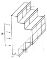
図15は、図14とは別の構成のX線撮像装置の従来技術の概略的斜視図である。なお、図15において、図14と同様の部分には、同一の符号を付している。
【0009】
図15のX線撮像装置では、ファイバープレート2の長さを変えて、たとえば3つの撮像素子1を一組として各組毎に段差を設けることによって、各撮像素子1に制御手段を設けられるようにしている。
【0010】
但し、蛍光体の大きさによっては周辺に位置する撮像素子1に設けられている制御手段にはX線が入射する場合があるので、これを防止するために撮像素子の周辺には、鉛などのX線遮蔽部材を設ける必要がある。
【0011】
しかし、図14に示すX線撮像装置では、ファイバープレート2を斜めに切断する加工が困難なこと、加えてロット当りの取り個数が少なくなるので価格が高くなる。また、傾斜を設けると、ファイバープレート2の各ファイバで光の伝送効率が悪くなりセンサの感度が低下する。
【0012】
さらに、図示したものは2×2ブロックのファイバープレート2を貼り合わせたもので、現有するファイバープレート2を使用すると100×100mm程度の大きさが限界である。
【0013】
しかるにファイバの傾斜を変えて3×3等にすると、各撮像素子内の画素のうち、中央に配置しているファイバープレートよりも、周辺に配置しているファイバープレートの方が光の透過率が劣り、各撮像素子から出力される信号にムラが生じる。
【0014】
一方、図15に示したX線撮像装置では、X線撮像装置が大型化したり、鉛などのX線遮蔽部材を備えたりすることで重量化する。また、各段差部分と撮像素子との位置合わせ精度が厳しいため、製造工数が多くなり、且つ高精度な位置合わせ装置が必要になる。
【0015】
図16は、X線撮像装置の感度を低下させずに、大型化、重量化、高コスト化の問題に適し、製造工程での作業性に優れた従来技術のX線撮像装置の模式的断面図である。
【0016】
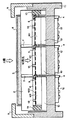
図16には、X線を可視光等の検知可能な波長の光に変換するシンチレータとしての蛍光体(波長変換手段)3と、蛍光体3によって変換された光を撮像素子1側へ導くと共に蛍光体3で変換しきれなかったX線を遮蔽する遮蔽材を含む複数の光ファイバからなるファイバープレート2と、隣接するファイバープレート2を接着する接着材7と、ファイバープレート2と撮像素子1とを接着する透明接着材6と、光を電気信号に変換する撮像素子1と、撮像素子1からの電気信号を外部に出力するフレキシブル基板4と、フレキシブル基板4と撮像素子1とを電気的に接続するバンプ5と、フレキシブル基板4が接続される電荷読み出し手段であるプリント基板12と、蛍光体3を保護するアルミニウムなどからなる保護シート8と、撮像素子1を搭載するベース基板10と、ベース基板10を保持するためのベース筐体11と、ベース筐体11に備えられた筐体カバー9と、撮像素子1とファイバープレート2との間に設けられた一定間隔を保持するためのスペーサ13と、撮像素子1を外気から遮断する封止樹脂15とを示している。
【0017】
本構成で示すX線撮像装置は、制御回路を各撮像素子1の画素間に配置したことで上記問題を解決している。
【0018】
また、プリント基板12と撮像素子1とを電気的に接続させるために、フレキシブル基板4を曲げて複数の隣接する撮像素子1間を通して接続させている。
【0019】
なお、図16に示すX線撮像装置は、複数のファイバープレート2が接着材7で接着されたファイバープレートと、複数の撮像素子1とを透明接着材6によって貼り合わせることによって製造する。
【0020】
或いは、図17に示すように、撮像素子1又はファイバープレート2の大きさなどを基準にしたX線撮像装置ユニットを複数貼り合わせることによって製造してもよい。
【0021】
図18は、図16の領域Yを拡大した模式的断面図である。図18において、401はインナーリード、402はフィルムとしてのベースフィルム、403はカバーフィルム、105は撮像素子1の端部とインナーリード401とのショートの防止及び撮像素子1の端部欠損を防止するポリイミド樹脂層などの有機絶縁層である。フレキシブル基板4はインナーリード401、ベースフィルム402及びカバーフィルム403である。
【0022】
ここで、図19(a)及び図19(b)を用いて、図18に示すバンプ5とフレキシブル基板4との従来の接続方法について説明する。
【0023】
図19は、図18に示すバンプ5とフレキシブル基板4との接続工程を示した模式的断面図である。
【0024】
はじめに、有機絶縁層105を25μmの厚さとなるように形成する。つぎに、バンプ5とフレキシブル基板4との電気的接続を行うために、撮像素子1に、スタッドバンプ方式やメッキなどによりバンプ5を形成する。
【0025】
そして、バンプ5とインナーリード401とを、たとえば超音波により金属間接合する。ここで、フレキシブル基板の総厚は、50μm程度としている。
【0026】
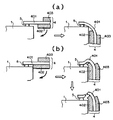
つぎに、撮像素子1を保持台17,18によって保持した状態で、治具19を保持台17,18の方向に或いは、保持台17、18を治具19の方向に移動させる。こうして、撮像素子1の端部に沿う様にインナーリード401を図面下側に向けて曲げる。
【0027】
【発明が解決しようとする課題】
しかし、従来の技術は、フレキシブル基板4を構成するベースフィルム402が外部接続端子であるバンプ5の撮像素子1(基板)からの厚みよりも厚く形成されているために、基板上までベースフィルム402を配することができなかった。従って、曲げた際にインナーリード401が基板に接してショートすることを防ぐために別途有機絶縁層105を設ける必要があり面倒であった。
【0028】
また、フレキシブル基板4を曲げるうえで、ベースフィルム402とバンプ5との位置関係が良好となるように位置合わせする必要があった。
【0029】
図20は、ベースフィルム402とバンプ5との位置関係が良好に位置合わせされて形成されたフレキシブル基板の模式的断面図である。
【0030】
図21(a),図21(b)は、それぞれベースフィルム402とバンプ5との位置合わせが良好でない場合を示したフレキシブル基板4の模式的断面図である。
【0031】
図21(a)に示すように、バンプ5に対してインナーリード401が所要の位置よりも基板1から離れて接する場合、インナーリード401が基板1と接してショートする或いは、基板1の端部で断線する恐れがある。
【0032】
一方、図21(b)に示すように、バンプ5に対してインナーリード401が所要の位置よりも基板1側で接する場合、ベースフィルム402が押し上げられてインナーリード401に引っ張り力が生じて、最悪の場合には、インナーリード401が断線する場合がある。
【0033】
また、図16において、ファイバープレート2から射出される光は拡散光であるからファイバープレート2と撮像素子1とのギャップが狭ければ狭いほど光は拡散せず高品位、高解像度のセンサが実現できる。従って、インナーリード401は薄ければ薄いほどよいが、位置合わせが良好でない場合はさらに断線しやすかった。
【0034】
そこで、本発明は、別途有機絶縁層を設けるという面倒な作業を行うことなく、高品位、高解像度の撮像装置或いは放射線撮像装置等を提供することを課題とする。
【0035】
【課題を解決するための手段】
上記課題を解決するために、本発明は、表面と側面とを有するシリコン基板からなり、前記表面に半導体素子と電気的に接続された外部接続端子を有する基板と、インナーリード及び前記インナーリードの少なくとも一部を覆うベースフィルムを有するフレキシブル基板と、を有する半導体装置の製造方法において、前記ベースフィルムの端と前記基板とを位置合わせする工程と、前記位置合わせをした状態で接着剤を用いて前記ベースフィルムと前記基板の側面とを接着する工程と、前記ベースフィルムと前記基板の側面とを接着させた後に、前記インナーリードを曲げて前記インナーリードを前記外部接続端子に接続させる工程と、を含む。
【0036】
また、本発明の半導体装置は、上記フレキシブル基板と、前記外部接続端子が形成された基板と、を有し、前記ベースフィルムのうち少なくとも前記基板上に配されている領域は前記外部接続端子よりも薄いことを特徴とする半導体装置。
【0037】
また、本発明の半導体装置は、上記フレキシブル基板と、前記外部接続端子が形成された基板と、を有し、前記基板の外部接続端子の外側の角が面取りされていることを特徴とする。
【0038】
さらに、本発明の撮像装置は、上記フレキシブル基板と、前記外部接続端子が形成された基板とを有し、前記基板が光電変換基板であることを特徴とする。
【0039】
さらにまた、本発明の撮像システムは、上記撮像装置が複数貼り合わされていることを特徴とする。
【0040】
また、本発明の放射線撮像装置は、上記撮像装置と、シンチレータとを備えることを特徴とする。
【0041】
さらに、本発明の放射線撮像システムは、上記放射線撮像装置と、前記放射線撮像装置からの信号を処理する信号処理手段と、前記信号処理手段からの信号を記録するための記録手段と、前記信号処理手段からの信号を表示するための表示手段と、前記信号処理手段からの信号を伝送するための伝送処理手段とを具備することを特徴とする。
【0042】
さらにまた、本発明の半導体装置の製造方法は、半導体素子及び外部接続端子が同一面に形成された基板と、インナーリード及び前記インナーリードの前記基板側を覆うフィルムで構成されたフレキシブル基板とを有する半導体装置の製造方法において、前記フィルムの先端と前記基板とを位置合わせする工程と、前記位置合わせをした状態で接着剤を用いて当該フィルムと前記基板の側壁とを接着する工程と、前記フィルムと前記基板の側面とを接着させた後に前記インナーリードを曲げて当該インナーリードを前記外部接続端子に接続させる工程とを含むことを特徴とする。
【0043】
またさらに、本発明の半導体装置は、基板と、基板上に形成された外部接続端子に一端が接続されたフレキシブル基板と、を有する半導体装置において、前記基板の外部接続端子の外側の角が面取りされていることを特徴とする。
【0044】
【発明の実施の形態】
以下、本発明の実施形態について図面を参照して説明する。
【0045】
(実施形態1)
図1は、本発明の実施形態1のフレキシブル基板を搭載した半導体装置の模式的断面図である。
【0046】
図1において、1は基板、4はインナーリード401及びフィルムとしてのベースフィルム402及びカバーフィルム403で構成されるフレキシブル基板、5は外部接続端子としてのバンプである。
【0047】
図1のフレキシブル基板4は、基板1上に形成されたバンプ5に一端が接続されていて、ベースフィルム402のうち基板1上に配されるベースフィルム402をバンプ5のよりも薄くしている。
【0048】
まず、図1に示すフレキシブル基板のベースフィルム402の基板1側の先端を、基板1に向かって段階的に薄くする具体的な方法について説明する。
【0049】
はじめに、ベースフィルム402となるポリイミドフィルム上に銅薄膜をスパッタ法により成膜する。つぎに、ホトレジストをポリイミドフィルムの両面に塗布し所望パターンを露光現像により得る。
【0050】
このとき銅箔面には電気配線パターン、非銅箔面にはポリイミドフィルム形状パターンを形成する。そして、めっき法により銅を必要なパターン部のみにめっき形成する。
【0051】
つぎに、エッチングによりポリイミドフィルムに穴を形成する。このときのエッチングを一度ハーフエッチングの段階で止める。そして、エッチングされた領域のうち段差形状として残したい領域にホトレジストを塗布して所望パターンを露光現象によって得る。
【0052】
そして、再度ポリイミドフィルムをエッチングをすることで、段差形状のベースフィルム402が得られる。最後にレジストを除去し、銅のフラッシュエッチングによりパターンを電気的に分離した後金めっきでフレキシブル基板とする。
【0053】
本実施形態では、基板1上に配されるフィルム領域を薄くすることで、基板1上にベースフィルム402を配することが可能となった。従って図18に示す有機絶縁層105は不要となり、製造するうえでの工程数が削減できる。
【0054】
なお、本明細書において、基板上に配するとは必ずしも基板1とベースフィルム402が接している必要はない。たとえば、ベースフィルム402が空間或いは別の材料を介して基板上に形成されていても配すると表する。
【0055】
さらには、バンプ5よりもベースフィルム402が薄いため、基板1の端部でベースフィルム402を曲げてもインナーリード401は押し上げられない。このためインナーリード401は引っ張り力が生じず断線しにくい。
【0056】
なお、ベースフィルム402は、たとえばポリイミドフィルムを材料としている。カバーフィルム403は、たとえばウレタンやポリイミドを材料としている。なお、これらの材料は、上記例に限定されるものでなく、曲げやすい柔らかい材料であればよい。
【0057】
また、基板1は、光を信号電荷に変換する撮像素子を有する光電変換基板であってもよい。その際は図示されていないが垂直シフトレジスタ、水平シフトレジスタを有し、基板の材質としてはシリコン基板或いはアモルファスシリコン基板であって、表面は二次元に配された複数の画素と、その上部にはシリコン酸化膜等を利用した層間絶縁層、アルミ等を利用した金属配線、窒化膜及び/又はポリイミド等を利用した保護層等から構成される。なお、画素はフォトダイオード及びMOSトランジスタ等で構成される。
【0058】
また、本発明のフレキシブル基板は基板上に形成されたバンプ5に接続させてもよいし、或いは、予めフレキシブル基板にバンプ5を形成した後に基板と接続させてもよい。
【0059】
(実施形態2)
図2は、本発明の実施形態2のフレキシブル基板を搭載した半導体装置の模式的断面図である。
【0060】
図2に示すフレキシブル基板4は、ベースフィルム402が基板上に配されるフィルム領域だけではなくベースフィルム402全体がバンプ5の厚さよりも薄い点で実施形態1と異なる。
【0061】
具体的には12μm程度のベースフィルム402にめっき法により18μm程度の厚さのインナーリード401を形成している。ちなみに、カバーフィルムは10μm程度の厚さになるように印刷法で形成している。
【0062】
また、インナーリード401はめっき法によって形成することによりベースフィルム402とインナーリード401間に接着材層が必要なくなりフレキシブル基板そのものを薄くすることができる。
【0063】
なお、従来はめっき法を利用していなかったためにベースフィルム或いはインナーリードを薄くすることが困難であった。
【0064】
以上説明したとおり、本実施形態のフレキシブル基板4によって、基板1上にベースフィルム402を配することが可能となる。従って図18に示す有機絶縁層105は不要となり、製造するうえでの工程数が削減できる。
【0065】
さらには、バンプ5よりもベースフィルム402が薄いため、基板1の端部でベースフィルム402を曲げてもインナーリード401は押し上げられない。このためインナーリード401は引っ張り力が生じず断線しにくい。
【0066】
また、ベースフィルム402全体を薄くすることで、たとえば図16に示すように隣接する複数の基板(撮像素子1)間或いは、撮像装置間をフレキシブル基板4が配する場合、隣接する基板間或いは、撮像装置間の間隔をより狭めることが可能となり、高品位、高解像度の撮像装置或いは放射線撮像装置が提供できる。
【0067】
また、本発明のフレキシブル基板は基板上に形成されたバンプ5に接続させてもよいし、或いは、予めフレキシブル基板にバンプ5を形成した後に基板と接続させてもよい。
【0068】
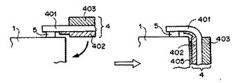
(実施形態3)
図3は、本発明の実施形態3のフレキシブル基板を搭載した半導体装置の模式的断面図である。
【0069】
図4は、本発明の実施形態3のフレキシブル基板の形成方法を示した模式的断面図である。
【0070】
図4において、410はベースフィルム402となるポリイミドフィルム、411は銅薄膜、412はホトレジスト、413はパターン銅めっき、414はポリイミドフィルム形状パターン、θはテーパー角である。
【0071】
なお、図3,図4において、図1等に示した部分と同様の部分には同一符号を付している。
【0072】
図3に示すフレキシブル基板4は、ベースフィルム402の基板側の先端が細くなるような傾斜形状である。
【0073】
傾斜形状とは、たとえば図3に示されるようにベースフィルム402の基板1側の先端が基板1側に向かって薄く形成されたテーパー形状等である。なお、図3には、ベースフィルム402の基板1側が傾斜している様子を図示しているが、ベースフィルム402のインナーリード401側が傾斜していてもよい。
【0074】
本実施形態においても、実施形態1及び2と同様に、基板1上にバンプ5の厚さよりも薄いベースフィルム403のフィルム領域を配することが可能となった。従って図18に示す有機絶縁層105は不要となり、製造するうえでの工程数が削減できる。
【0075】
さらには、バンプ5よりもベースフィルム402が薄いので基板1の端部でベースフィルム402を曲げてもインナーリード401は押し上げられないので引っ張り力が生じず、インナーリード401は断線しにくい。
【0076】
ここで、本実施形態のフレキシブル基板4の形成方法の一例として、ベースフィルム402の基板側の先端がテーパー形状であるフレキシブル基板を例に説明する。
【0077】
まずベースフィルム402となるポリイミドフィルム410を用意する(図4(a))。
【0078】
つぎに、ポリイミドフィルム410上に、銅薄膜411をスパッタ法により成膜する(図4(b))。
【0079】
さらに、ホトレジスト412をポリイミドフィルム410の両面一意に銅薄膜411を介して塗布する(図4(c))。
【0080】
こうして、所望パターンを露光現像により得る(図4(d))。
【0081】
このとき銅薄膜面には電気配線パターン、非銅薄膜面にはポリイミドフィルム形状パターン414が形成される(図4(e))。
【0082】
つぎにエッチングによりポリイミドフィルム410に穴を形成する。このときサイドエッチングによりポリイミドフィルム410の断面がテーパー形状となるようにエッチングする(図4(f))。
【0083】
そしてホトレジスト412及びポリイミドフィルム形状パターン414を除去する(図4(g))。
【0084】
銅のフラッシュエッチングによりパターンを電気的に分離した後に金めっきでフレキシブル基板を完成させる(図4(h))。
【0085】
以上説明したフレキシブル基板4の形成方法は、パターニング前にポリイミドフィルム410に穴を形成する方法に比べて配線パターニングが先なのでポリイイミドフイルム410が薄くてもパターンの形成が可能である。
【0086】
また、穴加工をエッチングにて行うことで断面がテーパー形状にできる。さらには、穴と配線パターンの位置精度が出しやすい。
【0087】
なお、テーパー角θは、バンプ5の厚さまでの傾斜形状を有しているベースフィルム402の領域が長い方が、基板1の端部と傾斜形状を有するベースフィルム402とのアライメントマージンが広がるので好適である。
【0088】
本実施形態では、テーパー角θを約18°としている。バンプ5の厚さを20μmとすれば、バンプ5の厚さまでの傾斜形状を有する領域は60μmであって、アライメントマージンは±30μmとなり特殊な装置がなくても位置合せが可能となる。
【0089】
テーパー角θを制御する方法としては、たとえば、ポリイミドフィルム410とホトレジストとしてのポリイミドフィルム形状パターン414との界面に進入するエッチング液のスピードで制御する。なお、テーパー角θを制御する方法は上記方法に限定されない。
【0090】
たとえば、ポリイミドフィルム410とホトレジストの密着度合いを制御することで界面へのエッチング液の進入度合いを変更することテーパー角θを制御できる。
【0091】
一例としては、ホトレジストに配合する密着強化剤の量を変更したり、ホトレジストのベーク温度を変更したりするなどである。たとえば、ベーク温度をさげることにより密着力が低下するのでテーパー角θは緩やかにできる。
【0092】
さらに、穴をあけたポリイミドフィルムに銅薄膜を接着剤にて貼り合せていた従来のフレキシブル基板に比べて、本実施形態の形成方法では接着剤を用いないので薄型化、柔軟性の面で好適である。
【0093】
また、本発明のフレキシブル基板は基板上に形成されたバンプ5に接続させてもよいし、或いは、予めフレキシブル基板にバンプ5を形成した後に基板と接続させてもよい。
【0094】
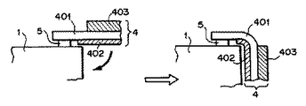
(実施形態4)
図5は、本発明の実施形態4の半導体装置の模式的断面図である。
【0095】
図5に示す半導体装置は、基板1の外部接続端子の外側の角を面取りしている。
【0096】
このようにすると、基板1の端部でベースフィルム402を曲げて基板1の側面に沿ってフレキシブル基板4を配しても、インナーリード401は押し上げられないので引っ張り力が生じず、インナーリード401が断線しにくい半導体装置となる。
【0097】
なお、本実施形態においてフレキシブル基板4のベースフィルム402の厚さは、バンプ5より厚くてもよいが、ベースフィルム402全体をバンプ5よりも薄くすることで、たとえば図16に示すように隣接する複数の基板(撮像素子1)間或いは、撮像装置間をフレキシブル基板4が配する場合、隣接する基板間或いは、撮像装置間の間隔をより狭めることが可能となり、高品位、高解像度の撮像装置或いは放射線撮像装置が提供できる。
【0098】
(実施形態5)
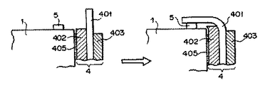
図6は、本発明の実施形態5の半導体装置の製造方法を示した模式的断面図である。
【0099】
図7は、曲げたフレキシブル基板4と基板1の側面とを接着させる工程をした模式的断面図である。
【0100】
図6において405は接着剤としての熱紫外線硬化型樹脂である。図7において406は紫外線源である。なお、図6,図7において図1等に示した部分と同様の部分には同一符号を付している。
【0101】
図6は、ベースフィルム402のバンプ5側の先端と基板1の光入射側とを位置合わせした状態で、撮像素子1の側面に熱紫外線硬化型樹脂405によってベースフィルム402を接続してからインナーリード401を曲げてバンプ5に接続した様子を示している。
【0102】
具体的には、本発明の半導体装置の製造方法は、ベースフィルム402のバンプ5に近い方の先端と基板1とを位置合わせする工程と、位置合わせした状態で熱紫外線硬化型樹脂405を用いてベースフィルム402と基板1の側壁端部とを接着させる工程と、接着させた後にインナーリード401を曲げてバンプ5に接続させる工程とを含む。
【0103】
こうすると、ベースフィルム402を予め位置合せできているので、インナーリード401と基板1とがショートすることがながなく、図18に示す有機絶縁層105は必要ない。また、インナーリード401が断線することもない。
【0104】
つぎに、基板1とベースフィルム402との接着工程について図7を用いて具体的に説明する。
【0105】
まず基板1の裏面側から、熱紫外線硬化型樹脂405をフレキシブル基板4と基板1との隙間に塗布し、それから熱紫外線硬化型樹脂405に紫外線源406から紫外線を照射すると共に加熱して、フレキシブル基板4と基板1の側面とを接着させる。
【0106】
なお、接着剤を紫外線照射するだけで硬化するものにすると、フレキシブル基板4と基板1との隙間には、紫外線が到達しにくく、未硬化接着剤が基板1に悪影響を及ぼす可能性があることや隙間の接着剤を硬化させるまでが面倒であるので、上記のように、硬化には熱紫外線効果型樹脂の接着剤を用いることが望ましい。
【0107】
また、接着剤としては厚みが予め決まっている接着剤シート等を用いてもよい。
【0108】
(実施形態6)
図8は、本発明の実施形態6の放射線撮像装置の模式的断面図である。
【0109】
図8に示す放射線撮像装置は、実施形態1〜3で説明したフレキシブル基板のいずれかを搭載している。
【0110】
図8において、3は放射線としてたとえばX線を可視光等の検知可能な波長の光に変換するシンチレータとしての蛍光体(波長変換手段)、101は光を電気信号に変換する撮像素子100を有する光電変換基板、2は蛍光体3によって変換された光を撮像素子100側へ導くと共に蛍光体3で変換しきれなかったX線を遮蔽する遮蔽材を含む複数の光ファイバからなるファイバープレート、7は隣接するファイバープレート2を接着する接着材7、6はファイバープレート2と光電変換基板101とを接着する透明接着材、4は撮像素子100からの電気信号を外部に出力するフレキシブル基板であって複数の光電変換基板101間を配してプリント基板12と電気的に接続されている。5はフレキシブル基板4と撮像素子100とを電気的に接続する外部接続端子としてのバンプ、12はフレキシブル基板4が接続される電荷読み出し手段であるプリント基板、8は蛍光体3を保護するアルミニウムなどからなる保護シート、10は光電変換基板101を搭載するベース基板、11はベース基板10を保持するためのベース筐体、9はベース筐体11に備えられた筐体カバー、13は光電変換基板101とファイバープレート2との間に設けられた一定間隔を保持するためのスペーサ13、15は光電変換基板101を外気から遮断する封止樹脂である。
【0111】
また、光電変換基板101とは、光を信号電荷に変換する撮像素子100を有する基板である。従って、図示していないが垂直シフトレジスタ、水平シフトレジスタを有し、基板の材質としてはシリコン基板或いはアモルファスシリコン基板であって、表面は二次元に配された複数の画素と、その上部にはシリコン酸化膜等を利用した層間絶縁層、アルミ等を利用した金属配線、窒化膜及び/又はポリイミド等を利用した保護層等を備えている。なお、画素はフォトダイオード及びMOSトランジスタ等で構成している。
【0112】
なお、本実施形態では放射線撮像装置について説明しているが、蛍光体3或いは蛍光体3とファイバープレート2がない構成の撮像装置であってもよい。
【0113】
また、本実施形態では複数の光電変換基板101を貼り合せた放射線撮像装置を示しているが光電変換基板101を1つのみ有する放射線撮像装置であってもよい。その際は、フレキシブル基板を曲げて形成することで光の入射面積に対し小さな断面積を有する放射線撮像装置が形成できる。
【0114】
又は、蛍光体3或いは蛍光体3とファイバープレート2がない構成であって、光電変換基板101を1つ有する撮像装置であってもよい。その際は、フレキシブル基板を曲げて形成することで光の入射方向に対して小型化された撮像装置が形成できる。
【0115】
ここで、図8を用いて本発明の放射線撮像装置としてのX線撮像装置の動作について説明する。蛍光体3側に図示しないX線源を設置し、さらに、X線源とX線撮像装置との間に被写体を位置させた状態で、X線源からX線を照射すると、そのX線は被写体に曝射される。
【0116】
すると、X線は被写体を透過するときに強度差を有するレントゲン情報を含んでX線撮像装置側に送られる。
【0117】
X線撮像装置側では、到達したX線のほとんどが蛍光体3において、X線の強度に応じた可視光等の光に変換される。変換されることで得られた光は、ファイバープレート2を通じて光電変換基板101へ伝送される。
【0118】
このとき、ファイバープレート2と光電変換基板101とが透明接着材6によって接着されているため、光は透明接着材6を通過するときに減衰することなく撮像素子100に入射される。
【0119】
一方、X線撮像装置側へ到達したX線のうち、蛍光体3で変換しきれなかったX線や、蛍光体3へ入射しないX線は、撮像素子100で検知できる波長に変換されないまま、撮像素子100側へ進行する。
【0120】
このようなX線は、ファイバープレート2に含まれる遮蔽材によって遮蔽され、撮像素子100やプリント基板12へ入射しない。
【0121】
また、光は、接着材7にも入射される。接着材7に入射した光は、吸収又は反射等されて光の透過率が小さくなる。この光が撮像素子100の画素上に入射されるとライン欠陥になるが、上述したように、ファイバープレート2の大きさと光電変換基板101との大きさを同じにして、これらを位置合わせすると接着材7からの光が撮像素子100の画素に影響を与えにくい構成とすることができる。
【0122】
撮像素子100では、入射された光を、光の強度に応じた電気信号に変換する。この電気信号は、図示しない読み出し回路の指示に応じて、バンプ5を介してフレキシブル基板4に読み出される。フレキシブル基板4に読み出された電気信号は、図示しない外部回路基板に送られ、A/D変換された後に画像処理がされる。
【0123】
ここで、図9、図10及び図11を用いて本発明の放射線撮像装置の製造工程について説明する。
【0124】
図9は、本発明の実施形態6の放射線撮像装置の製造工程において、本発明のフレキシブル基板が搭載された光電変換基板101とベース基板との接着工程を示した模式的断面図である。
【0125】
図10は、本発明の実施形態6の放射線撮像装置の製造工程において、本発明のフレキシブル基板が搭載された光電変換基板101とファイバープレートとの貼り合わせ工程を示した図である。
【0126】
図11は、実施形態6の放射線撮像装置の製造工程において、本発明のフレキシブル基板が搭載された光電変換基板101とファイバープレートとの貼り合わせ工程を示した図である。
【0127】
それぞれの工程について説明する。まず、フレキシブル基板4を備えた複数の光電変換基板101を、X,Y,Z方向及びθ(回転)方向に可動するアライメントヘッド及びアライメントカメラを用いて位置合わせしながらステージ上に載置する。このとき、各光電変換基板101は、ステージに形成されている孔からバキューム装置などで吸引されることによってステージ上に固定される(図9(a))。
【0128】
この状態で、各光撮像素子100が所要の動作を行うかどうかの検査を行う。この検査では、検査治具を用いて、たとえば静電気などによって各撮像素子100が破壊されているかどうかなどを調べる(図9(b))。
【0129】
そして、検査の結果、撮像素子100に欠陥が発見されれば、その光電変換基板101の下方のバキューム装置をオフして、アライメントヘッドを用いて交換する(図9(c))。
【0130】
つづいて、光電変換基板101上に、紫外線硬化型又はシリコン樹脂などの接着材を塗布する(図9(d))。
【0131】
そして、ベース基板10に設けられた長孔にフレキシブル基板4を挿入し、それから光電変換基板101とベース基板10とを密着させた後に紫外線を照射及び/又は加圧することによって接着させる(図9(e))。
【0132】
なお、図9(e)に示すように、ファイバープレート2の大きさと光電変換基板101との大きさを同じにして、これらを位置合わせするとよい。また、ここでは、ベース基板10には、光電変換101との間における熱膨張率などを考量して、ガラス又はパーマアロイ(鉄+ニッケル)合金を用いている。
【0133】
そして、光電変換基板101とベース基板10とを接着した後に、バキューム装置をオフにして、ステージなどの治具から光電変換基板101及びベース基板10を取り外す(図9(f))。
【0134】
つぎに図10(a)から図10(d)を用いて、光電変換基板とファイバープレートとの貼り合わせ工程ついて説明する。まずベース基板10と接着した各光電変換基板101上に、各光電変換基板101とファイバープレート2との間隔を保持できるように、スペーサ13を配置する(図10(a))。
【0135】
なお、スペーサ13は球でも円柱形状でもよい。つぎに、シール材及び目地うめ接着材を、基板1上に塗布する(図10(b))。
【0136】
目地うめ接着材は光電変換基板101間の隙間を埋めるるために充填されるものである。シール材は、図10(b)に示すように一部が開口されており、後述するように、ここから真空注入の方式を用いて透明接着材6を充填する。注入する際、真空リークの原因とならぬように目地うめ接着材を光電変換基板101間の隙間に充填している。それから、スペーサ13上に、ファイバープレート2を貼り合わせる(図10(c))。
【0137】
さらにファイバープレート2を相互に接着する接着材7が、各光電変換基板101間の隙間若しくは各画素間の直上に配置されるように行うとより好ましい。加圧、加熱プレスにより光電変換基板101とファイバープレートの間隔を均一にし、シール材を硬化させる。そして、真空チャンバー内で、ファイバープレートと各光電変換基板101との隙間を真空状態にしたところで、透明接着材6を溜めたボートに開口部分をつけ真空状態を大気圧に戻すことで、透明接着材6が隙間に充填される。その後、開口部分を封止する(図10(d))。
【0138】
それから、ファイバープレート2とベース基板10との間に封止樹脂15を塗布して、光電変換基板101を外気と遮断できるようにしている。
【0139】
さらに、たとえばシート上の蛍光体3をファイバープレート2上に貼りつけることによって、X線撮像装置が形成される。
【0140】
なお、蛍光体3はファイバープレート上に蒸着する手法や粉末状の蛍光体を結合材に混合させて塗布することによって設けることもできるが、この場合、図10(c)を用いて説明した工程の前に、ファイバープレート上に蛍光体3を設けておく。
【0141】
また、複数のX線撮像ユニットからX線撮像装置を製造する場合について図11(a)〜図11(d)に示すような工程によって光電変換基板101及びベース基板10とファイバープレートとを貼り合わせればよい。
【0142】
すなわち、ファイバープレート2を、光電変換基板101の面積に合わせて研磨し、且つ光入出射面も両面研磨して平坦化する。そして、ベース基板10と接着した各光電変換基板101上に、各光電変換基板101とファイバープレート2との間隔を保持できるように、球や円柱形状などのスペーサ13を配置する(図11(a))。
【0143】
つぎに、シール材14を、光電変換基板101上に塗布する(図11(b))。
【0144】
シール材は、図11(b)に示すように一部が開口されており、後述するように、ここから真空注入の方式を用いて透明接着材6を充填する。注入する際、真空リークの原因とならぬように目地うめ接着材を光電変換基板101間の隙間に充填している。ファイバープレート2をスペーサ13上に、位置決めした後にファイバープレート2と光電変換基板101を互いに加圧、加熱して貼り合わせる(図11(c))。
【0145】
そして、真空チャンバー内で、各ファイバープレート2と各光電変換基板101との隙間を真空状態にしたところで、透明接着材6を溜めたボートに開口部分をつけ真空状態を大気圧に戻すことで、透明接着材6が隙間に充填される。その後、開口部分を封止する(図11(d))。
【0146】
また、ファイバープレート2の光入射面側にある蛍光体3は蒸着、塗布、又は印刷により形成され、その工程はファイバープレート2の研磨後或いは光電変換基板101との貼り合わせ後のいずれかで行う。
【0147】
(実施形態7)
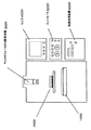
図12は、実施形態6で説明した放射線撮像装置を備えた非破壊検査システムの構成を示す概念図である。図12には、実施形態1で説明したX線撮像装置1000と、たとえば電気機器に組み込まれる非破壊検査対象物である被写体2000と、被写体2000にX線を照射するマイクロフォーカスX線発生器3000と、X線撮像装置1000から出力される信号を処理する画像処理装置6000と、画像処理装置6000によって処理された画像を表示するモニタ4000と、画像処理装置6000及びモニタ4000を操作するコントローラ5000とを示している。
【0148】
図12に示す非破壊検査システムは、マイクロフォーカスX線発生器3000によって発生されたX線を、非破壊検査を行いたい被写体2000に照射すると、被写体2000の内部における破壊の有無の情報が、X線撮像装置1000を通じて画像処理装置6000に出力される。画像処理装置6000では、出力された信号を、前述している各撮像素子1の周辺画素間の画像信号を処理したり、ダーク補正などを施して、モニタ4000に画像として表示する。
【0149】
モニタ4000に表示されている画像は、コントローラ5000によって指示を入力することで、たとえば拡大又は縮小したり、濃淡の制御等を行うことができる。こうして、モニタ4000に表示された画像を通じて、被写体2000の内部における破壊の有無を検査する。そして、被写体2000に破壊が発見されなければ、それを良品とみなして電気機器に組み込む。一方、被写体2000に破壊が発見されれば、それを不良品とみなして製造工程から除外する。
【0150】
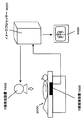
(実施形態8)
図13は、本発明のX線撮像装置を備えたX線診断システムの構成を示す概念図である。図13には、X線撮像装置1000を備えたベッドと、被写体2000にX線を照射するためのX線発生装置7000と、X線撮像装置1000から出力される画像信号の処理及びX線発生装置7000からのX線の照射時期等を制御するイメージプロセッサー8000と、イメージプロセッサー8000によって処理された画像信号を表示するモニタ4000とを示している。なお、図13において、図12で示した部分と同様の部分には、同一の符号を付している。
【0151】
図13に示すX線診断システムは、X線発生装置7000は、イメージプロセッサー8000からの指示に基づいてX線を発生させ、このX線をベッド上の被写体2000に照射すると、被写体2000のレントゲン情報がX線撮像装置1000を通じてイメージプロセッサー8000に出力される。イメージプロセッサー8000では、出力された信号を、前述している各撮像素子1の周辺画素間の画像信号を処理したり、ダーク補正などを施して、図示しないメモリに格納したり、モニタ4000に画像として表示する。
【0152】
モニタ4000に表示されている画像は、イメージプロセッサー8000によって指示を入力することで、たとえば拡大又は縮小したり、濃淡の制御等を行うことができる。こうして、モニタ4000に表示された画像を通じて、医師が被写体2000を診察する。
【0153】
また、医師が診察した後の被写体2000のレントゲン情報は、本システムの記録手段を設けて、ディスク状の記録媒体などに記録するようにしてもよい。
【0154】
なお、以上説明した本発明の各実施形態では、X線を用いた場合を例に説明したが、α,β,γ線等の放射線を用いることができる。また、光は画素により検出可能な波長領域の電磁波であり、可視光を含む。さらに、たとえば放射線を含む電磁波を電気信号に変換する電磁波電気信号変換装置にも適用することができる。
【0155】
さらに、各実施形態では光電変換装置等を例に説明したが、たとえば表示素子基板を複数平面的に貼り合わせるような大画面の表示装置にも同様に適用することができる。
【0156】
【発明の効果】
以上説明したように、本発明によると、別途有機絶縁層を設けるという面倒な作業を行うことなく、高品位、高解像度の撮像装置或いは放射線撮像装置等を提供することができる。
【図面の簡単な説明】
【図1】本発明の実施形態1のフレキシブル基板を搭載した半導体装置の模式的断面図である。
【図2】本発明の実施形態2のフレキシブル基板を搭載した半導体装置の模式的断面図である。
【図3】本発明の実施形態3のフレキシブル基板を搭載した半導体装置の模式的断面図である。
【図4】本発明の実施形態3のフレキシブル基板の形成方法を示した模式的断面図である。
【図5】本発明の実施形態4の半導体装置の模式的断面図である。
【図6】本発明の実施形態5の半導体装置の製造方法を示した模式的断面図である。
【図7】フレキシブル基板と基板の側面とを接着させる工程を示した模式的断面図である。
【図8】本発明の実施形態6として、実施形態1、2及び3で示した本発明のフレキシブル基板を搭載した放射線撮像装置の模式的断面図である。
【図9】本発明の実施形態6の放射線撮像装置の製造工程において、本発明のフレキシブル基板が搭載された基板とベース基板との接着工程を示した模式的断面図である。
【図10】本発明の実施形態6の放射線撮像装置の製造工程において、本発明のフレキシブル基板が搭載された基板とファイバープレートとの貼り合わせ工程を示した図である。
【図11】本発明の実施形態6の放射線撮像装置の製造工程において、本発明のフレキシブル基板が搭載された光電変換基板101とファイバープレートとの貼り合わせ工程を示した図である。
【図12】本発明の実施形態6で説明した放射線撮像装置を備えた非破壊検査システムの構成を示す概念図である。
【図13】本発明のX線撮像装置を備えたX線診断システムの構成を示す概念図である。
【図14】従来から知られているX線撮像装置の概略的断面図である。
【図15】別の構成のX線撮像装置の従来技術の概略的斜視図である。
【図16】図14及び図15のX線撮像装置の問題を解決した従来技術のX線撮像装置の模式的断面図である。
【図17】撮像素子1又はファイバープレート2の大きさなどを基準にしたX線撮像装置ユニットの模式的断面図である。
【図18】図16の領域Yを拡大した模式的断面図である。
【図19】図18に示すバンプとフレキシブル基板との接続工程を示した模式的断面図である。
【図20】ベースフィルムとバンプとの位置関係が良好となるように位置合わせされて形成されたフレキシブル基板の模式的断面図である。
【図21】ベースフィルムとバンプとの位置合わせが良好でない場合を示したフレキシブル基板の模式的断面図である。
【符号の説明】
1 基板
2 ファイバープレート
3 蛍光体(波長変換手段)
4 フレキシブル基板
5 バンプ
6 透明接着材
7 接着材
8 保護シート
9 筐体カバー
10 ベース基板
11 ベース筐体
12 プリント基板
13 スペーサ
14 シール材
15 封止樹脂[0001]
BACKGROUND OF THE INVENTION
The present invention relates to a flexible substrate, a semiconductor device, an imaging device, a radiation imaging device, and a radiation imaging system, and in particular, a flexible substrate such as a medical X-ray imaging device or an industrial nondestructive device, a radiation imaging device, and a radiation imaging system. About.
[0002]
In the present specification, the category of radiation includes electromagnetic waves such as X-rays, α-rays, β-rays, and γ-rays.
[0003]
[Prior art]
2. Description of the Related Art Conventionally, there is a need for a radiation imaging apparatus, particularly an X-ray imaging apparatus for medical purposes, which is capable of X-ray moving images, has excellent image quality, is thin, and has a large area input range. In addition, not only for medical use, but also for industrial nondestructive inspection machines and the like, a thin and inexpensive large-area X-ray imaging apparatus is required.
[0004]
As such an X-ray imaging apparatus, for example, there is an X-ray imaging apparatus having a large area so that a non-light-receiving part of a CCD sensor does not interfere by providing a step in the thickness of the fiber plate.
[0005]
FIG. 14 is a schematic cross-sectional view of a conventionally known X-ray imaging apparatus.
[0006]
In FIG. 14, a
[0007]
Although not shown, this X-ray imaging apparatus includes a
[0008]
FIG. 15 is a schematic perspective view of a conventional technique of an X-ray imaging apparatus having a configuration different from that of FIG. In FIG. 15, the same parts as those in FIG. 14 are denoted by the same reference numerals.
[0009]
In the X-ray imaging apparatus of FIG. 15, the length of the
[0010]
However, depending on the size of the phosphor, X-rays may be incident on the control means provided in the image pickup device 1 located in the vicinity. Therefore, in order to prevent this, lead or the like is placed around the image pickup device. It is necessary to provide an X-ray shielding member.
[0011]
However, in the X-ray imaging apparatus shown in FIG. 14, it is difficult to cut the
[0012]
Further, the illustrated one is a laminate of 2 × 2 blocks of
[0013]
However, if the inclination of the fiber is changed to 3 × 3 or the like, among the pixels in each imaging element, the fiber plate arranged in the periphery has a light transmittance rather than the fiber plate arranged in the center. Inferior, the signal output from each image sensor is uneven.
[0014]
On the other hand, in the X-ray imaging apparatus shown in FIG. 15, the X-ray imaging apparatus is increased in size and weighted by including an X-ray shielding member such as lead. Further, since the alignment accuracy between each stepped portion and the image sensor is severe, the number of manufacturing steps is increased and a highly accurate alignment apparatus is required.
[0015]
FIG. 16 is a schematic cross-sectional view of a conventional X-ray imaging apparatus that is suitable for the problems of upsizing, weight, and cost increase without degrading the sensitivity of the X-ray imaging apparatus and that is excellent in workability in the manufacturing process. FIG.
[0016]
FIG. 16 shows a phosphor (wavelength conversion means) 3 as a scintillator that converts X-rays into light having a detectable wavelength such as visible light, and guides the light converted by the
[0017]
The X-ray imaging apparatus shown in this configuration solves the above problem by arranging a control circuit between the pixels of each imaging element 1.
[0018]
Further, in order to electrically connect the
[0019]
The X-ray imaging apparatus shown in FIG. 16 is manufactured by bonding a fiber plate in which a plurality of
[0020]
Alternatively, as shown in FIG. 17, a plurality of X-ray imaging device units based on the size of the imaging element 1 or the
[0021]
FIG. 18 is a schematic cross-sectional view in which a region Y in FIG. 16 is enlarged. In FIG. 18, 401 is an inner lead, 402 is a base film as a film, 403 is a cover film, 105 is a short circuit between the end of the image sensor 1 and the
[0022]
Here, a conventional method for connecting the bump 5 and the
[0023]
FIG. 19 is a schematic cross-sectional view showing a connection process between the bump 5 and the
[0024]
First, the organic insulating
[0025]
Then, the bump 5 and the
[0026]
Next, in a state where the imaging device 1 is held by the holding
[0027]
[Problems to be solved by the invention]
However, in the conventional technique, since the
[0028]
Further, when the
[0029]
FIG. 20 is a schematic cross-sectional view of a flexible substrate formed with a good positional relationship between the
[0030]
FIGS. 21A and 21B are schematic cross-sectional views of the
[0031]
As shown in FIG. 21A, when the
[0032]
On the other hand, as shown in FIG. 21B, when the
[0033]
In FIG. 16, since the light emitted from the
[0034]
Therefore, an object of the present invention is to provide a high-quality, high-resolution imaging device or radiation imaging device without performing a troublesome task of separately providing an organic insulating layer.
[0035]
[Means for Solving the Problems]
In order to solve the above problems, the present invention provides:A substrate having an external connection terminal electrically connected to a semiconductor element on the surface; a flexible substrate having an inner lead and a base film covering at least a part of the inner lead; In the method of manufacturing a semiconductor device, the step of aligning the end of the base film and the substrate, and the base film and the side surface of the substrate are bonded using an adhesive in the aligned state. And a step of bonding the base film and the side surface of the substrate and then bending the inner lead to connect the inner lead to the external connection terminal.
[0036]
Moreover, the semiconductor device of the present invention includes the flexible substrate and a substrate on which the external connection terminal is formed, and at least a region of the base film disposed on the substrate is from the external connection terminal. A thin semiconductor device.
[0037]
According to another aspect of the present invention, there is provided a semiconductor device including the flexible substrate and a substrate on which the external connection terminal is formed, and an outer corner of the external connection terminal of the substrate is chamfered.
[0038]
Furthermore, the imaging device of the present invention includes the flexible substrate and a substrate on which the external connection terminal is formed, and the substrate is a photoelectric conversion substrate.
[0039]
Furthermore, the imaging system of the present invention is characterized in that a plurality of the imaging devices are bonded together.
[0040]
Moreover, the radiation imaging device of this invention is provided with the said imaging device and a scintillator.
[0041]
Furthermore, the radiation imaging system of the present invention includes the radiation imaging apparatus, a signal processing means for processing a signal from the radiation imaging apparatus, a recording means for recording a signal from the signal processing means, and the signal processing. A display means for displaying a signal from the means; and a transmission processing means for transmitting the signal from the signal processing means.
[0042]
Furthermore, the semiconductor device manufacturing method of the present invention includes a substrate on which a semiconductor element and an external connection terminal are formed on the same surface, and a flexible substrate configured by an inner lead and a film covering the substrate side of the inner lead. In the manufacturing method of the semiconductor device having, the step of aligning the tip of the film and the substrate, the step of bonding the film and the side wall of the substrate using an adhesive in the aligned state, A step of bonding the film and a side surface of the substrate and then bending the inner lead to connect the inner lead to the external connection terminal.
[0043]
Furthermore, the semiconductor device of the present invention is a semiconductor device having a substrate and a flexible substrate having one end connected to an external connection terminal formed on the substrate, and the outer corner of the external connection terminal of the substrate is chamfered. It is characterized by being.
[0044]
DETAILED DESCRIPTION OF THE INVENTION
Embodiments of the present invention will be described below with reference to the drawings.
[0045]
(Embodiment 1)
FIG. 1 is a schematic cross-sectional view of a semiconductor device on which a flexible substrate according to Embodiment 1 of the present invention is mounted.
[0046]
In FIG. 1, 1 is a substrate, 4 is a flexible substrate composed of an
[0047]
The
[0048]
First, a specific method for gradually thinning the tip of the
[0049]
First, a copper thin film is formed on a polyimide film to be the
[0050]
At this time, an electric wiring pattern is formed on the copper foil surface, and a polyimide film shape pattern is formed on the non-copper foil surface. Then, copper is plated only on a necessary pattern portion by a plating method.
[0051]
Next, holes are formed in the polyimide film by etching. The etching at this time is stopped once at the half etching stage. And a photoresist is apply | coated to the area | region to leave as a step shape among the etched areas, and a desired pattern is obtained by the exposure phenomenon.
[0052]
Then, the step-shaped
[0053]
In the present embodiment, the
[0054]
Note that in this specification, the substrate 1 and the
[0055]
Furthermore, since the
[0056]
The
[0057]
The substrate 1 may be a photoelectric conversion substrate having an image sensor that converts light into signal charges. In this case, although not shown in the drawing, it has a vertical shift register and a horizontal shift register, and the substrate material is a silicon substrate or an amorphous silicon substrate, and the surface is a plurality of pixels arranged two-dimensionally, and an upper portion thereof. Is composed of an interlayer insulating layer using a silicon oxide film or the like, a metal wiring using aluminum or the like, a protective layer using a nitride film and / or polyimide or the like. The pixel is composed of a photodiode, a MOS transistor, and the like.
[0058]
The flexible substrate of the present invention may be connected to the bumps 5 formed on the substrate, or may be connected to the substrate after the bumps 5 are formed on the flexible substrate in advance.
[0059]
(Embodiment 2)
FIG. 2 is a schematic cross-sectional view of a semiconductor device on which a flexible substrate according to
[0060]
The
[0061]
Specifically, an
[0062]
Further, by forming the
[0063]
Conventionally, since the plating method has not been used, it has been difficult to make the base film or the inner lead thin.
[0064]
As described above, the
[0065]
Furthermore, since the
[0066]
Further, by thinning the
[0067]
The flexible substrate of the present invention may be connected to the bumps 5 formed on the substrate, or may be connected to the substrate after the bumps 5 are formed on the flexible substrate in advance.
[0068]
(Embodiment 3)
FIG. 3 is a schematic cross-sectional view of a semiconductor device on which a flexible substrate according to
[0069]
FIG. 4 is a schematic cross-sectional view showing a flexible substrate forming method according to
[0070]
In FIG. 4, 410 is a polyimide film to be the
[0071]
3 and 4, the same reference numerals are given to the same parts as those shown in FIG.
[0072]
The
[0073]
The inclined shape is, for example, a tapered shape in which the tip of the
[0074]
Also in the present embodiment, as in the first and second embodiments, it is possible to dispose a film region of the
[0075]
Furthermore, since the
[0076]
Here, as an example of the method for forming the
[0077]
First, a
[0078]
Next, a copper
[0079]
Further, a
[0080]
Thus, a desired pattern is obtained by exposure and development (FIG. 4D).
[0081]
At this time, an electrical wiring pattern is formed on the copper thin film surface, and a polyimide
[0082]
Next, a hole is formed in the
[0083]
Then, the
[0084]
After the pattern is electrically separated by flash etching of copper, the flexible substrate is completed by gold plating (FIG. 4 (h)).
[0085]
The method for forming the
[0086]
Moreover, a cross section can be made into a taper shape by performing a hole process by an etching. Furthermore, the positional accuracy of the hole and the wiring pattern is easily obtained.
[0087]
The taper angle θ is such that the longer the region of the
[0088]
In this embodiment, the taper angle θ is about 18 °. If the thickness of the bump 5 is 20 μm, the region having an inclined shape up to the thickness of the bump 5 is 60 μm, and the alignment margin is ± 30 μm, so that alignment is possible without a special device.
[0089]
As a method for controlling the taper angle θ, for example, the taper angle θ is controlled by the speed of the etchant entering the interface between the
[0090]
For example, the taper angle θ can be controlled by controlling the degree of adhesion between the
[0091]
For example, the amount of the adhesion enhancing agent blended in the photoresist is changed, or the baking temperature of the photoresist is changed. For example, since the adhesive force is reduced by lowering the baking temperature, the taper angle θ can be made gentle.
[0092]
Furthermore, compared to the conventional flexible substrate in which a copper thin film is bonded to a polyimide film with a hole by an adhesive, the formation method of this embodiment does not use an adhesive, so it is suitable in terms of thickness reduction and flexibility. It is.
[0093]
The flexible substrate of the present invention may be connected to the bumps 5 formed on the substrate, or may be connected to the substrate after the bumps 5 are formed on the flexible substrate in advance.
[0094]
(Embodiment 4)
FIG. 5 is a schematic cross-sectional view of a semiconductor device according to
[0095]
In the semiconductor device shown in FIG. 5, the outer corners of the external connection terminals of the substrate 1 are chamfered.
[0096]
In this way, even if the
[0097]
In the present embodiment, the thickness of the
[0098]
(Embodiment 5)
FIG. 6 is a schematic cross-sectional view showing a method for manufacturing a semiconductor device according to Embodiment 5 of the present invention.
[0099]
FIG. 7 is a schematic cross-sectional view showing a process of bonding the bent
[0100]
In FIG. 6,
[0101]
FIG. 6 shows a state in which the tip of the
[0102]
Specifically, the method for manufacturing a semiconductor device of the present invention uses the step of aligning the tip of the
[0103]
In this way, since the
[0104]
Next, the bonding process between the substrate 1 and the
[0105]
First, the thermal ultraviolet
[0106]
If the adhesive is cured by simply irradiating it with ultraviolet rays, it is difficult for the ultraviolet rays to reach the gap between the
[0107]
Further, as the adhesive, an adhesive sheet having a predetermined thickness may be used.
[0108]
(Embodiment 6)
FIG. 8 is a schematic cross-sectional view of the radiation imaging apparatus according to the sixth embodiment of the present invention.
[0109]
The radiation imaging apparatus shown in FIG. 8 is equipped with any of the flexible substrates described in the first to third embodiments.
[0110]
In FIG. 8, 3 is a phosphor (wavelength converting means) as a scintillator that converts, for example, X-rays into light having a detectable wavelength such as visible light, and 101 has an
[0111]
The
[0112]
Although the radiation imaging apparatus has been described in the present embodiment, the imaging apparatus may be configured such that the
[0113]
Further, in the present embodiment, a radiation imaging apparatus in which a plurality of
[0114]
Alternatively, the image pickup apparatus may have a configuration in which the
[0115]
Here, the operation of the X-ray imaging apparatus as the radiation imaging apparatus of the present invention will be described with reference to FIG. When an X-ray source (not shown) is installed on the
[0116]
Then, the X-ray is sent to the X-ray imaging apparatus side including X-ray information having an intensity difference when passing through the subject.
[0117]
On the X-ray imaging apparatus side, most of the X-rays that have reached are converted into light such as visible light according to the intensity of the X-rays in the
[0118]
At this time, since the
[0119]
On the other hand, among the X-rays that have reached the X-ray imaging apparatus side, X-rays that could not be converted by the
[0120]
Such X-rays are shielded by the shielding material included in the
[0121]
The light is also incident on the adhesive 7. The light incident on the adhesive 7 is absorbed or reflected, and the light transmittance is reduced. When this light is incident on the pixels of the
[0122]
In the
[0123]
Here, the manufacturing process of the radiation imaging apparatus of the present invention will be described with reference to FIGS.
[0124]
FIG. 9 is a schematic cross-sectional view showing a bonding process between the
[0125]
FIG. 10 is a diagram illustrating a bonding process between the
[0126]
FIG. 11 is a diagram illustrating a bonding process between the
[0127]
Each step will be described. First, a plurality of
[0128]
In this state, it is inspected whether each
[0129]
If a defect is found in the
[0130]
Subsequently, an adhesive such as an ultraviolet curable resin or a silicon resin is applied on the photoelectric conversion substrate 101 (FIG. 9D).
[0131]
Then, the
[0132]
In addition, as shown in FIG.9 (e), it is good to make the magnitude | size of the
[0133]
Then, after the
[0134]
Next, the bonding process between the photoelectric conversion substrate and the fiber plate will be described with reference to FIGS. First, spacers 13 are arranged on each
[0135]
The
[0136]
The joint filler adhesive is filled to fill a gap between the
[0137]
Furthermore, it is more preferable that the adhesive 7 for bonding the
[0138]
Then, a sealing
[0139]
Further, for example, an X-ray imaging apparatus is formed by attaching the
[0140]
The
[0141]
Further, in the case of manufacturing an X-ray imaging apparatus from a plurality of X-ray imaging units, the
[0142]
That is, the
[0143]
Next, the sealing
[0144]
As shown in FIG. 11B, a part of the sealing material is opened, and as will be described later, the transparent adhesive 6 is filled from here using a vacuum injection method. When injecting, the joint adhesive material is filled in the gap between the
[0145]
In the vacuum chamber, when the gap between each
[0146]
The
[0147]
(Embodiment 7)
FIG. 12 is a conceptual diagram illustrating a configuration of a nondestructive inspection system including the radiation imaging apparatus described in the sixth embodiment. FIG. 12 shows the
[0148]
In the nondestructive inspection system shown in FIG. 12, when the subject 2000 to be subjected to the nondestructive inspection is irradiated with the X-rays generated by the microfocus X-ray generator 3000, information on the presence or absence of destruction inside the subject 2000 is X The image is output to the image processing apparatus 6000 through the
[0149]
The image displayed on the
[0150]
(Embodiment 8)
FIG. 13 is a conceptual diagram showing a configuration of an X-ray diagnostic system including the X-ray imaging apparatus of the present invention. FIG. 13 shows a bed including the
[0151]
In the X-ray diagnostic system shown in FIG. 13, the X-ray generator 7000 generates X-rays based on an instruction from the image processor 8000 and irradiates the subject 2000 on the bed with the X-ray information of the subject 2000. Is output to the image processor 8000 through the
[0152]
The image displayed on the
[0153]
Further, the X-ray information of the subject 2000 after the doctor examines may be recorded on a disk-shaped recording medium or the like by providing recording means of this system.
[0154]
In each of the embodiments of the present invention described above, the case where X-rays are used has been described as an example. However, radiation such as α, β, and γ rays can be used. Light is an electromagnetic wave in a wavelength region that can be detected by a pixel, and includes visible light. Furthermore, for example, the present invention can be applied to an electromagnetic wave electric signal conversion device that converts an electromagnetic wave including radiation into an electric signal.
[0155]
Furthermore, in each embodiment, the photoelectric conversion device or the like has been described as an example. However, the present invention can be similarly applied to a large-screen display device in which a plurality of display element substrates are bonded in a planar manner.
[0156]
【The invention's effect】
As described above, according to the present invention, it is possible to provide a high-quality, high-resolution imaging apparatus or radiation imaging apparatus or the like without performing the troublesome task of providing a separate organic insulating layer.
[Brief description of the drawings]
FIG. 1 is a schematic cross-sectional view of a semiconductor device on which a flexible substrate according to a first embodiment of the present invention is mounted.
FIG. 2 is a schematic cross-sectional view of a semiconductor device on which a flexible substrate according to
FIG. 3 is a schematic cross-sectional view of a semiconductor device on which a flexible substrate according to a third embodiment of the present invention is mounted.
FIG. 4 is a schematic cross-sectional view showing a flexible substrate forming method according to a third embodiment of the present invention.
FIG. 5 is a schematic cross-sectional view of a semiconductor device according to a fourth embodiment of the present invention.
FIG. 6 is a schematic cross-sectional view showing a method for manufacturing a semiconductor device according to a fifth embodiment of the present invention.
FIG. 7 is a schematic cross-sectional view showing a process of bonding a flexible substrate and a side surface of the substrate.
FIG. 8 is a schematic cross-sectional view of a radiation imaging apparatus on which the flexible substrate of the present invention shown in
FIG. 9 is a schematic cross-sectional view showing a bonding step between a substrate on which a flexible substrate of the present invention is mounted and a base substrate in a manufacturing process of a radiation imaging apparatus according to a sixth embodiment of the present invention.
FIG. 10 is a diagram showing a bonding process between a substrate on which a flexible substrate of the present invention is mounted and a fiber plate in a manufacturing process of a radiation imaging apparatus according to a sixth embodiment of the present invention.
FIG. 11 is a diagram showing a bonding process between a
FIG. 12 is a conceptual diagram illustrating a configuration of a nondestructive inspection system including the radiation imaging apparatus described in the sixth embodiment of the present invention.
FIG. 13 is a conceptual diagram showing a configuration of an X-ray diagnostic system including the X-ray imaging apparatus of the present invention.
FIG. 14 is a schematic cross-sectional view of a conventionally known X-ray imaging apparatus.
FIG. 15 is a schematic perspective view of a related art X-ray imaging apparatus having another configuration.
16 is a schematic cross-sectional view of a conventional X-ray imaging apparatus that solves the problem of the X-ray imaging apparatus of FIGS. 14 and 15. FIG.
17 is a schematic cross-sectional view of an X-ray imaging apparatus unit based on the size of the imaging element 1 or the
FIG. 18 is a schematic cross-sectional view in which a region Y in FIG. 16 is enlarged.
FIG. 19 is a schematic cross-sectional view showing a connection process between the bump and the flexible substrate shown in FIG. 18;
FIG. 20 is a schematic cross-sectional view of a flexible substrate formed by being aligned so that the positional relationship between the base film and the bumps is good.
FIG. 21 is a schematic cross-sectional view of a flexible substrate showing a case where the alignment between the base film and the bump is not good.
[Explanation of symbols]
1 Substrate
2 Fiber plate
3 phosphor (wavelength conversion means)
4 Flexible substrate
5 Bump
6 Transparent adhesive
7 Adhesive
8 Protection sheet
9 Case cover
10 Base substrate
11 Base housing
12 Printed circuit board
13 Spacer
14 Sealing material
15 Sealing resin
Claims (3)
インナーリード及び前記インナーリードの少なくとも一部を覆うベースフィルムを有するフレキシブル基板と、を有する半導体装置の製造方法において、 In a method of manufacturing a semiconductor device having an inner lead and a flexible substrate having a base film covering at least a part of the inner lead,
前記ベースフィルムの端と前記基板とを位置合わせする工程と、 Aligning the end of the base film and the substrate;
前記位置合わせをした状態で接着剤を用いて前記ベースフィルムと前記基板の側面とを接着する工程と、 Bonding the base film and the side surface of the substrate using an adhesive in the aligned state;
前記ベースフィルムと前記基板の側面とを接着させた後に、前記インナーリードを曲げて前記インナーリードを前記外部接続端子に接続させる工程と、を含むことを特徴とする半導体装置の製造方法。 And a step of bonding the base film and the side surface of the substrate and then bending the inner lead to connect the inner lead to the external connection terminal.
Priority Applications (1)
| Application Number | Priority Date | Filing Date | Title |
|---|---|---|---|
| JP2002161865A JP4100965B2 (en) | 2001-06-13 | 2002-06-03 | Manufacturing method of semiconductor device |
Applications Claiming Priority (3)
| Application Number | Priority Date | Filing Date | Title |
|---|---|---|---|
| JP2001-178844 | 2001-06-13 | ||
| JP2001178844 | 2001-06-13 | ||
| JP2002161865A JP4100965B2 (en) | 2001-06-13 | 2002-06-03 | Manufacturing method of semiconductor device |
Publications (3)
| Publication Number | Publication Date |
|---|---|
| JP2003133654A JP2003133654A (en) | 2003-05-09 |
| JP2003133654A5 JP2003133654A5 (en) | 2005-10-06 |
| JP4100965B2 true JP4100965B2 (en) | 2008-06-11 |
Family
ID=26616844
Family Applications (1)
| Application Number | Title | Priority Date | Filing Date |
|---|---|---|---|
| JP2002161865A Expired - Fee Related JP4100965B2 (en) | 2001-06-13 | 2002-06-03 | Manufacturing method of semiconductor device |
Country Status (1)
| Country | Link |
|---|---|
| JP (1) | JP4100965B2 (en) |
Cited By (1)
| Publication number | Priority date | Publication date | Assignee | Title |
|---|---|---|---|---|
| WO2014091970A1 (en) | 2012-12-12 | 2014-06-19 | オリンパス株式会社 | Connection structure for semiconductor device, ultrasonic module, and ultrasonic endoscope system having built-in ultrasonic module |
Families Citing this family (8)
| Publication number | Priority date | Publication date | Assignee | Title |
|---|---|---|---|---|
| JP4209762B2 (en) * | 2003-12-12 | 2009-01-14 | パナソニック株式会社 | Imaging device |
| JP4871629B2 (en) * | 2006-04-12 | 2012-02-08 | キヤノン株式会社 | Radiation imaging apparatus manufacturing method and radiation imaging system |
| JP4855168B2 (en) * | 2006-07-27 | 2012-01-18 | オリンパス株式会社 | Solid-state imaging device |
| KR101761817B1 (en) | 2011-03-04 | 2017-07-26 | 삼성전자주식회사 | Large-scale x-ray detector |
| JP2012227404A (en) * | 2011-04-21 | 2012-11-15 | Sumitomo Electric Printed Circuit Inc | Flexible printed wiring board |
| JP6231778B2 (en) * | 2013-06-05 | 2017-11-15 | キヤノン株式会社 | Electrical device and radiation inspection equipment |
| KR20190040245A (en) * | 2016-12-28 | 2019-04-17 | 가부시키가이샤후지쿠라 | A wiring body assembly, a wiring board, and a touch sensor |
| CN113241352B (en) * | 2021-05-19 | 2024-03-15 | 中国科学院长春光学精密机械与物理研究所 | Wire-bonding flexible circuit board for packaging image sensor and preparation process thereof |
-
2002
- 2002-06-03 JP JP2002161865A patent/JP4100965B2/en not_active Expired - Fee Related
Cited By (2)
| Publication number | Priority date | Publication date | Assignee | Title |
|---|---|---|---|---|
| WO2014091970A1 (en) | 2012-12-12 | 2014-06-19 | オリンパス株式会社 | Connection structure for semiconductor device, ultrasonic module, and ultrasonic endoscope system having built-in ultrasonic module |
| US9997449B2 (en) | 2012-12-12 | 2018-06-12 | Olympus Corporation | Semiconductor device connection structure, ultrasonic module, and ultrasonic endoscope system having ultrasonic module |
Also Published As
| Publication number | Publication date |
|---|---|
| JP2003133654A (en) | 2003-05-09 |
Similar Documents
| Publication | Publication Date | Title |
|---|---|---|
| US6800857B2 (en) | Large-area fiber plate, radiation image pickup apparatus utilizing the same and producing method therefor | |
| US6800836B2 (en) | Image pickup device, radiation image pickup device and image processing system | |
| JP3595759B2 (en) | Imaging apparatus and imaging system | |
| US7193218B2 (en) | Radiation detection device, method of producing the same, and radiation image pick-up system | |
| TWI408828B (en) | Radiation photography device | |
| US6909173B2 (en) | Flexible substrate, semiconductor device, imaging device, radiation imaging device and radiation imaging system | |
| US7050538B2 (en) | Radiation imaging apparatus and radiation imaging system using the same | |
| US7564112B2 (en) | Semiconductor device, radiographic imaging apparatus, and method for manufacturing the same | |
| JP4871629B2 (en) | Radiation imaging apparatus manufacturing method and radiation imaging system | |
| JP2007071836A (en) | Radiation detector, and radiation imaging system | |
| JP4100965B2 (en) | Manufacturing method of semiconductor device | |
| JP2006278877A (en) | Radiation imager and its manufacturing method | |
| JP4346865B2 (en) | Image input device, manufacturing method thereof, and radiation imaging system using image input device | |
| WO2018123189A1 (en) | Radiation imaging device, method for manufacturing radiation imaging device, and imaging system | |
| JP4693297B2 (en) | Radiation imaging apparatus and radiation imaging system | |
| JP2007057428A (en) | Radiation detecting device and radiation imaging system | |
| WO2019198318A1 (en) | Imaging device, electronic apparatus, and method for manufacturing imaging device | |
| KR20190054363A (en) | A method of manufacturing a curved detector and A curved detector | |
| JP2003066148A (en) | Imaging device, radiation imaging device and image processing system | |
| JP2004085456A (en) | Radiation imaging device and radiation imaging system | |
| JP2002164523A (en) | Radiation image pickup device and its manufacturing method | |
| JP3997134B2 (en) | Fiber plate and manufacturing method thereof, radiation imaging apparatus, and radiation imaging system | |
| JP2003270351A (en) | Radiography device | |
| JP2003004854A (en) | Radiation detector and radiation detection system | |
| JP2002048871A (en) | Image pickup device, radiation detection device, and image processing system |
Legal Events
| Date | Code | Title | Description |
|---|---|---|---|
| A521 | Request for written amendment filed |
Free format text: JAPANESE INTERMEDIATE CODE: A523 Effective date: 20050527 |
|
| A621 | Written request for application examination |
Free format text: JAPANESE INTERMEDIATE CODE: A621 Effective date: 20050527 |
|
| A977 | Report on retrieval |
Free format text: JAPANESE INTERMEDIATE CODE: A971007 Effective date: 20070625 |
|
| A131 | Notification of reasons for refusal |
Free format text: JAPANESE INTERMEDIATE CODE: A131 Effective date: 20070816 |
|
| A521 | Request for written amendment filed |
Free format text: JAPANESE INTERMEDIATE CODE: A523 Effective date: 20071012 |
|
| TRDD | Decision of grant or rejection written | ||
| A01 | Written decision to grant a patent or to grant a registration (utility model) |
Free format text: JAPANESE INTERMEDIATE CODE: A01 Effective date: 20080314 |
|
| A61 | First payment of annual fees (during grant procedure) |
Free format text: JAPANESE INTERMEDIATE CODE: A61 Effective date: 20080318 |
|
| FPAY | Renewal fee payment (event date is renewal date of database) |
Free format text: PAYMENT UNTIL: 20110328 Year of fee payment: 3 |
|
| R150 | Certificate of patent or registration of utility model |
Free format text: JAPANESE INTERMEDIATE CODE: R150 |
|
| FPAY | Renewal fee payment (event date is renewal date of database) |
Free format text: PAYMENT UNTIL: 20120328 Year of fee payment: 4 |
|
| FPAY | Renewal fee payment (event date is renewal date of database) |
Free format text: PAYMENT UNTIL: 20130328 Year of fee payment: 5 |
|
| FPAY | Renewal fee payment (event date is renewal date of database) |
Free format text: PAYMENT UNTIL: 20140328 Year of fee payment: 6 |
|
| LAPS | Cancellation because of no payment of annual fees |