JP4078014B2 - Nonvolatile semiconductor memory device and manufacturing method thereof - Google Patents
Nonvolatile semiconductor memory device and manufacturing method thereof Download PDFInfo
- Publication number
- JP4078014B2 JP4078014B2 JP2000161126A JP2000161126A JP4078014B2 JP 4078014 B2 JP4078014 B2 JP 4078014B2 JP 2000161126 A JP2000161126 A JP 2000161126A JP 2000161126 A JP2000161126 A JP 2000161126A JP 4078014 B2 JP4078014 B2 JP 4078014B2
- Authority
- JP
- Japan
- Prior art keywords
- insulating film
- film
- gate
- field effect
- region
- Prior art date
- Legal status (The legal status is an assumption and is not a legal conclusion. Google has not performed a legal analysis and makes no representation as to the accuracy of the status listed.)
- Expired - Fee Related
Links
- 239000004065 semiconductor Substances 0.000 title claims description 96
- 238000004519 manufacturing process Methods 0.000 title claims description 25
- 230000002093 peripheral effect Effects 0.000 claims description 141
- 229910021420 polycrystalline silicon Inorganic materials 0.000 claims description 129
- 230000015654 memory Effects 0.000 claims description 126
- VYPSYNLAJGMNEJ-UHFFFAOYSA-N Silicium dioxide Chemical compound O=[Si]=O VYPSYNLAJGMNEJ-UHFFFAOYSA-N 0.000 claims description 121
- IJGRMHOSHXDMSA-UHFFFAOYSA-N Atomic nitrogen Chemical compound N#N IJGRMHOSHXDMSA-UHFFFAOYSA-N 0.000 claims description 64
- 239000011229 interlayer Substances 0.000 claims description 61
- 238000000034 method Methods 0.000 claims description 57
- 230000005669 field effect Effects 0.000 claims description 45
- 239000000758 substrate Substances 0.000 claims description 40
- 238000002955 isolation Methods 0.000 claims description 37
- 229910052757 nitrogen Inorganic materials 0.000 claims description 33
- 238000000151 deposition Methods 0.000 claims description 29
- 238000007254 oxidation reaction Methods 0.000 claims description 25
- 229910052698 phosphorus Inorganic materials 0.000 claims description 25
- 230000003647 oxidation Effects 0.000 claims description 24
- OAICVXFJPJFONN-UHFFFAOYSA-N Phosphorus Chemical compound [P] OAICVXFJPJFONN-UHFFFAOYSA-N 0.000 claims description 23
- 239000011574 phosphorus Substances 0.000 claims description 23
- 239000010410 layer Substances 0.000 claims description 22
- 238000009792 diffusion process Methods 0.000 claims description 14
- 238000009279 wet oxidation reaction Methods 0.000 claims description 14
- 230000015572 biosynthetic process Effects 0.000 claims description 11
- 230000015556 catabolic process Effects 0.000 claims description 7
- 239000011159 matrix material Substances 0.000 claims description 6
- 238000000137 annealing Methods 0.000 claims description 5
- 230000001590 oxidative effect Effects 0.000 claims description 3
- 229910052814 silicon oxide Inorganic materials 0.000 claims 23
- 229920005591 polysilicon Polymers 0.000 claims 4
- 238000003491 array Methods 0.000 claims 2
- 239000003990 capacitor Substances 0.000 claims 1
- 229910052681 coesite Inorganic materials 0.000 description 49
- 229910052906 cristobalite Inorganic materials 0.000 description 49
- 239000000377 silicon dioxide Substances 0.000 description 49
- 235000012239 silicon dioxide Nutrition 0.000 description 49
- 229910052682 stishovite Inorganic materials 0.000 description 49
- 229910052905 tridymite Inorganic materials 0.000 description 49
- 229910004298 SiO 2 Inorganic materials 0.000 description 37
- 238000001459 lithography Methods 0.000 description 19
- 238000004518 low pressure chemical vapour deposition Methods 0.000 description 18
- QGZKDVFQNNGYKY-UHFFFAOYSA-N Ammonia Chemical compound N QGZKDVFQNNGYKY-UHFFFAOYSA-N 0.000 description 16
- KRHYYFGTRYWZRS-UHFFFAOYSA-N Fluorane Chemical compound F KRHYYFGTRYWZRS-UHFFFAOYSA-N 0.000 description 14
- 230000008021 deposition Effects 0.000 description 13
- 229910052581 Si3N4 Inorganic materials 0.000 description 12
- 238000001312 dry etching Methods 0.000 description 12
- 239000007789 gas Substances 0.000 description 12
- HQVNEWCFYHHQES-UHFFFAOYSA-N silicon nitride Chemical compound N12[Si]34N5[Si]62N3[Si]51N64 HQVNEWCFYHHQES-UHFFFAOYSA-N 0.000 description 12
- 230000008569 process Effects 0.000 description 11
- 239000007864 aqueous solution Substances 0.000 description 9
- 238000005468 ion implantation Methods 0.000 description 8
- 229910021529 ammonia Inorganic materials 0.000 description 7
- 239000002184 metal Substances 0.000 description 7
- 230000007423 decrease Effects 0.000 description 5
- 230000006866 deterioration Effects 0.000 description 5
- 230000000694 effects Effects 0.000 description 5
- 238000005516 engineering process Methods 0.000 description 5
- 238000000059 patterning Methods 0.000 description 4
- 229920002120 photoresistant polymer Polymers 0.000 description 4
- 238000010586 diagram Methods 0.000 description 3
- 238000009826 distribution Methods 0.000 description 3
- 125000004433 nitrogen atom Chemical group N* 0.000 description 3
- 239000002356 single layer Substances 0.000 description 3
- NBIIXXVUZAFLBC-UHFFFAOYSA-N Phosphoric acid Chemical compound OP(O)(O)=O NBIIXXVUZAFLBC-UHFFFAOYSA-N 0.000 description 2
- BLRPTPMANUNPDV-UHFFFAOYSA-N Silane Chemical compound [SiH4] BLRPTPMANUNPDV-UHFFFAOYSA-N 0.000 description 2
- 230000003247 decreasing effect Effects 0.000 description 2
- 238000006731 degradation reaction Methods 0.000 description 2
- 230000006870 function Effects 0.000 description 2
- 239000012535 impurity Substances 0.000 description 2
- 230000014759 maintenance of location Effects 0.000 description 2
- 230000009467 reduction Effects 0.000 description 2
- XUIMIQQOPSSXEZ-UHFFFAOYSA-N Silicon Chemical compound [Si] XUIMIQQOPSSXEZ-UHFFFAOYSA-N 0.000 description 1
- 230000002159 abnormal effect Effects 0.000 description 1
- 239000002253 acid Substances 0.000 description 1
- 229910000147 aluminium phosphate Inorganic materials 0.000 description 1
- 238000004380 ashing Methods 0.000 description 1
- QVGXLLKOCUKJST-UHFFFAOYSA-N atomic oxygen Chemical compound [O] QVGXLLKOCUKJST-UHFFFAOYSA-N 0.000 description 1
- 230000008901 benefit Effects 0.000 description 1
- 230000008859 change Effects 0.000 description 1
- 238000005229 chemical vapour deposition Methods 0.000 description 1
- 238000007796 conventional method Methods 0.000 description 1
- 230000007547 defect Effects 0.000 description 1
- 238000005530 etching Methods 0.000 description 1
- 239000002784 hot electron Substances 0.000 description 1
- 125000004435 hydrogen atom Chemical group [H]* 0.000 description 1
- 238000002347 injection Methods 0.000 description 1
- 239000007924 injection Substances 0.000 description 1
- 229910000069 nitrogen hydride Inorganic materials 0.000 description 1
- 239000001301 oxygen Substances 0.000 description 1
- 229910052760 oxygen Inorganic materials 0.000 description 1
- 238000005498 polishing Methods 0.000 description 1
- 229910052710 silicon Inorganic materials 0.000 description 1
- 239000010703 silicon Substances 0.000 description 1
- 238000003860 storage Methods 0.000 description 1
- 239000000126 substance Substances 0.000 description 1
- 238000001039 wet etching Methods 0.000 description 1
Images


Classifications
-
- H—ELECTRICITY
- H10—SEMICONDUCTOR DEVICES; ELECTRIC SOLID-STATE DEVICES NOT OTHERWISE PROVIDED FOR
- H10B—ELECTRONIC MEMORY DEVICES
- H10B69/00—Erasable-and-programmable ROM [EPROM] devices not provided for in groups H10B41/00 - H10B63/00, e.g. ultraviolet erasable-and-programmable ROM [UVEPROM] devices
-
- H—ELECTRICITY
- H10—SEMICONDUCTOR DEVICES; ELECTRIC SOLID-STATE DEVICES NOT OTHERWISE PROVIDED FOR
- H10B—ELECTRONIC MEMORY DEVICES
- H10B41/00—Electrically erasable-and-programmable ROM [EEPROM] devices comprising floating gates
- H10B41/40—Electrically erasable-and-programmable ROM [EEPROM] devices comprising floating gates characterised by the peripheral circuit region
-
- H—ELECTRICITY
- H01—ELECTRIC ELEMENTS
- H01L—SEMICONDUCTOR DEVICES NOT COVERED BY CLASS H10
- H01L27/00—Devices consisting of a plurality of semiconductor or other solid-state components formed in or on a common substrate
- H01L27/02—Devices consisting of a plurality of semiconductor or other solid-state components formed in or on a common substrate including semiconductor components specially adapted for rectifying, oscillating, amplifying or switching and having at least one potential-jump barrier or surface barrier; including integrated passive circuit elements with at least one potential-jump barrier or surface barrier
- H01L27/04—Devices consisting of a plurality of semiconductor or other solid-state components formed in or on a common substrate including semiconductor components specially adapted for rectifying, oscillating, amplifying or switching and having at least one potential-jump barrier or surface barrier; including integrated passive circuit elements with at least one potential-jump barrier or surface barrier the substrate being a semiconductor body
- H01L27/10—Devices consisting of a plurality of semiconductor or other solid-state components formed in or on a common substrate including semiconductor components specially adapted for rectifying, oscillating, amplifying or switching and having at least one potential-jump barrier or surface barrier; including integrated passive circuit elements with at least one potential-jump barrier or surface barrier the substrate being a semiconductor body including a plurality of individual components in a repetitive configuration
- H01L27/105—Devices consisting of a plurality of semiconductor or other solid-state components formed in or on a common substrate including semiconductor components specially adapted for rectifying, oscillating, amplifying or switching and having at least one potential-jump barrier or surface barrier; including integrated passive circuit elements with at least one potential-jump barrier or surface barrier the substrate being a semiconductor body including a plurality of individual components in a repetitive configuration including field-effect components
-
- H—ELECTRICITY
- H01—ELECTRIC ELEMENTS
- H01L—SEMICONDUCTOR DEVICES NOT COVERED BY CLASS H10
- H01L29/00—Semiconductor devices adapted for rectifying, amplifying, oscillating or switching, or capacitors or resistors with at least one potential-jump barrier or surface barrier, e.g. PN junction depletion layer or carrier concentration layer; Details of semiconductor bodies or of electrodes thereof ; Multistep manufacturing processes therefor
- H01L29/66—Types of semiconductor device ; Multistep manufacturing processes therefor
- H01L29/68—Types of semiconductor device ; Multistep manufacturing processes therefor controllable by only the electric current supplied, or only the electric potential applied, to an electrode which does not carry the current to be rectified, amplified or switched
- H01L29/76—Unipolar devices, e.g. field effect transistors
- H01L29/772—Field effect transistors
- H01L29/78—Field effect transistors with field effect produced by an insulated gate
- H01L29/788—Field effect transistors with field effect produced by an insulated gate with floating gate
-
- H—ELECTRICITY
- H10—SEMICONDUCTOR DEVICES; ELECTRIC SOLID-STATE DEVICES NOT OTHERWISE PROVIDED FOR
- H10B—ELECTRONIC MEMORY DEVICES
- H10B41/00—Electrically erasable-and-programmable ROM [EEPROM] devices comprising floating gates
- H10B41/40—Electrically erasable-and-programmable ROM [EEPROM] devices comprising floating gates characterised by the peripheral circuit region
- H10B41/42—Simultaneous manufacture of periphery and memory cells
- H10B41/49—Simultaneous manufacture of periphery and memory cells comprising different types of peripheral transistor
-
- H—ELECTRICITY
- H10—SEMICONDUCTOR DEVICES; ELECTRIC SOLID-STATE DEVICES NOT OTHERWISE PROVIDED FOR
- H10B—ELECTRONIC MEMORY DEVICES
- H10B99/00—Subject matter not provided for in other groups of this subclass
Description
【0001】
【発明の属する技術分野】
本発明は、不揮発性半導体記憶装置及びその製造方法に係り、その微細化,低電圧動作,高信頼化,製造工程の簡略化を図る技術に関する。
【0002】
【従来の技術】
不揮発性半導体記憶装置の代表であるフラッシュメモリは、携帯性,耐衝撃性に優れ、オンボードで電気的に一括消去が可能なことから、携帯電話,デジタルカメラ等の小型携帯情報機器のメモリとして急速に市場を拡大している。
【0003】
フラッシュメモリは、例えば図18に示したように、通常、情報を蓄えるメモリセルMと、書換えや読出しを行なうビットを選択したり、チップ内部で必要な電圧を発生する周辺回路を構成するMOS型電界効果トランジスタPから成る。
【0004】
このうちメモリセルMは、ソース及びドレイン拡散層(図示せず)を有するシリコン(Si)基板201と、このSi基板上に形成したPウェル204aと、主に多結晶Si膜からなる浮遊ゲート207及び制御ゲート209と、この両ゲート間を分離する多結晶Si層間絶縁膜208と、浮遊ゲート207とPウェル204aを分離するトンネル絶縁膜206からなるMOS型電界効果トランジスタを1つの記憶単位とし、これを複数個行列状に配置して構成される。メモリセルの浮遊ゲートと制御ゲートを分離する多結晶Si層間絶縁膜には、通常、SiO2膜に比べて誘電率が大きくリーク電流の小さい、シリコン窒化(Si3N4)膜をSiO2膜で挟んだ積層膜、いわゆるONO膜が広く用いられている。
【0005】
周辺回路Pは、Si基板201中に形成されたPウェル204b,Nウェル205と、ソース及びドレイン拡散層212a,212bと、ウェル上にゲート絶縁膜210を介して形成した主に多結晶Si膜からなるゲート電極211からなるMOS型電界効果トランジスタを複数個組み合わせることにより構成される。ゲート絶縁膜210は通常、熱酸化法により形成されたSiO2膜が用いられている。
【0006】
各メモリセルM及び周辺回路トランジスタPは、通常、厚い酸化膜からなる素子分離領域202により分離される。そして周辺回路により発生した正または負の電圧を制御ゲート209に印加することにより浮遊ゲートに蓄積される電荷量を制御し、これによりメモリセルトランジスタのしきい値電圧を変化させることにより情報の“0”,“1”を判別している。
【0007】
【発明が解決しようとする課題】
しかしながら、上記した不揮発性半導体記憶装置の大容量化に伴い、周辺回路用MOSトランジスタP及びメモリセルMに新たな課題が生じてきた。
【0008】
第1点は、周辺回路用MOSトランジスタのゲート酸化膜劣化に起因した特性及び信頼性の劣化である。
【0009】
フラッシュメモリにおいては、書込み/消去の際、ワード線に例えば18Vといった高電圧が印加される。このような高電圧を扱う周辺回路用MOSトランジスタにおいては、ゲート酸化膜厚を例えば25nm程度と厚膜化することにより高耐圧を図っている。しかしながら、素子の微細化のために、周辺MOSトランジスタ間の素子分離に従来の選択酸化法(LOCOS)に代えて浅溝分離法を適用した場合、25nmといった厚いゲート酸化膜を熱酸化法により形成すると、浅溝分離領域部に接するゲート酸化膜厚がアクティブ領域に比べ著しく薄くなるという現象が生じた。このため、MOSトランジスタの電流−電圧特性にいわゆるキンクを生じたり、ゲート酸化膜の絶縁耐圧が低下するといった問題を生じた。
【0010】
第2点は、プログラム電圧低減に不可欠なメモリセルMの多結晶Si層間絶縁膜の薄膜化である。
【0011】
フラッシュメモリの書換え動作時に浮遊ゲートに印加される電圧Vfgは、
Vfg=C2・Vcg/(C1+C2) (1)
で与えられる。ここで、Vcgは制御ゲート印加電圧、 C1及びC2はそれぞれトンネル絶縁膜及び多結晶Si層間絶縁膜の容量である。制御ゲートに印加された電圧を効率良く浮遊ゲートに伝達し、プログラム電圧を低減するためにはC2を大きくする、つまり、多結晶Si層間絶縁膜を薄膜化することが有効である。しかしながら、従来から広く用いられているシリコン窒化(Si3N4)膜をSiO2膜で挟んだ積層膜、いわゆるONO膜では、上下層のSiO2膜を5nm以下とすると、浮遊ゲートに蓄積された電荷が制御ゲートに漏洩するいわゆるリテンション不良が顕在化するという問題があった。また、上層のSiO2膜を5nm形成しようとした場合、下層の多結晶Si膜の酸化を防止するために10nm程度以上のSi3N4膜を堆積する必要があった。そのため、ONO膜の薄膜化は酸化膜換算で15nm程度が限界であった。
【0012】
このため、ONO膜に代えて、窒素を添加した単層のCVDSiO2膜を多結晶Si層間絶縁膜に適用し、その薄膜化を図ることによりプログラム電圧を低減する技術が特開平9−238036に開示されている。
【0013】
しかしながら、従来のフラッシュメモリで広く行われているように、多結晶Si層間絶縁膜を形成した後、熱酸化法により周辺回路MOSトランジスタのゲート酸化膜を形成すると、ONO膜とは異なり単層のCVDSiO2膜は耐酸化性を有しないため、高濃度に不純物がドーピングされた浮遊ゲート多結晶Siが厚く酸化されてしまうという問題があった。従って、メモリセル多結晶Si層間絶縁膜に単層のCVDSiO2膜を用いた際の周辺回路MOSトランジスタのゲート酸化膜の作成方法の開発が必要であった。
【0014】
第3点は工程数の増大である。
【0015】
従来のフラッシュメモリでは、メモリセルのトンネル絶縁膜206,多結晶Si層間絶縁膜208及び周辺回路MOSトランジスタのゲート絶縁膜210を、順次、それぞれ単独に形成していた。このため工程数が多く、低コスト化を阻害する要因となっていた。最近では、フラッシュメモリの書換え速度及び読出し速度の向上を図るため、周辺回路領域のMOSトランジスタのゲート酸化膜厚を2種類とする技術も提案されており、今後、フラッシュメモリの製造工程の簡略化は重要な課題になると予想される。
【0016】
上述の3つの課題は、メモリセルの層間絶縁膜と周辺回路MOSトランジスタのゲート酸化膜の作成という観点で相互に密接に関係しており、これを解決するための新たな不揮発性半導体記憶装置及びその製造方法の開発が望まれていた。
【0017】
本発明の目的は、不揮発性半導体記憶装置の周辺回路領域MOSトランジスタのゲート酸化膜を高信頼化し、トランジスタ特性を向上することにある。
【0018】
本発明の別の目的は、不揮発性半導体記憶装置の微細化,低電圧化に対応した多結晶Si層間絶縁膜及び周辺回路領域MOSトランジスタのゲート酸化膜形成方法を提供することにある。
【0019】
本発明の更に別の目的は、不揮発性半導体記憶装置の製造工程の簡略化を図ることにある。
【0020】
【課題を解決するための手段】
上記第1の課題を解決するため、本発明の不揮発性半導体記憶装置では、周辺回路を構成するMOS型電界効果型トランジスタのゲート絶縁膜を半導体基板上に堆積して形成した絶縁膜、例えばCVDSiO2膜により形成する。これにより、MOS型電界効果型トランジスタ間の素子分離に浅溝分離法を用いても浅溝分離領域に接する部分のゲート酸化膜厚が薄くなることがなく、MOS型電界効果型トランジスタ特性におけるキンクを防止することができ、また、ゲート酸化膜の絶縁耐圧の低下を回避することができる。なお、周辺回路が2種類以上のゲート絶縁膜厚を有するMOS型電界効果型トランジスタから構成されている場合、ゲート絶縁膜厚が厚いほうの高電圧部のMOS型電界効果型トランジスタに適用すると特に有効である。
【0021】
また、周辺回路を構成するMOS型電界効果型トランジスタのゲート絶縁膜を、半導体基板表面を熱酸化した絶縁膜と該絶縁膜の上に堆積して形成した絶縁膜の積層膜(例えば、CVDSiO2膜)とすることにより、浅溝分離領域に接する部分のゲート酸化膜厚を堆積絶縁膜にて補償することができるので、上記堆積絶縁膜単層とした場合と同様に、MOS型電界効果型トランジスタ特性におけるキンクを防止することができ、また、ゲート酸化膜の絶縁耐圧の低下を回避することができる。なお、この場合には熱酸化絶縁膜の膜厚よりも堆積絶縁膜の膜厚のほうを厚くすることが効果達成上より好ましい。
【0022】
上記第2の課題を解決するために、本発明の不揮発性半導体記憶装置の製造方法では、周辺回路を構成するMOS型電界効果型トランジスタのゲート絶縁膜を半導体基板上に堆積した絶縁膜、例えばCVDSiO2膜により形成する。これにより、多結晶シリコン層間絶縁膜をCVDSiO2膜とし、多結晶シリコン層間絶縁膜を形成した後にゲート絶縁膜を形成した場合でも、多結晶シリコン層間絶縁膜のCVDSiO2膜が厚く酸化されてしまうことが回避できる。
【0023】
また、周辺回路のゲート絶縁膜の全部又は一部を熱酸化膜とする場合には、半導体基板表面を熱酸化する工程を多結晶シリコン層間絶縁膜を形成する工程よりも前に行ってしまうことにより、多結晶シリコン層間絶縁膜であるCVDSiO2膜の異常酸化を防止することができる。
【0024】
上記第3の課題を解決するために、本発明の不揮発性半導体記憶装置及びその製造方法では、多結晶シリコン層間絶縁膜形成のために堆積した絶縁膜、例えばCVD絶縁膜を、周辺回路を構成するMOS型電界効果型トランジスタのゲート絶縁膜の全部または一部として用いることにより、製造工程の簡略化を達成することができる。
【0025】
【発明の実施の形態】
(実施例1)
本実施例1では、不揮発性半導体記憶装置のメモリセルの多結晶Si層間絶縁膜と周辺回路MOSトランジスタのゲート酸化膜とを窒素を添加したCVDSiO2膜とし、これを同時に形成することにより、周辺回路MOSトランジスタの特性向上とメモリセルの微細化,動作電圧の低減及び製造工程の簡略化を図った例について説明する。
【0026】
本実施例の不揮発性半導体記憶装置の作成手順を図1及び図2に示す。不揮発性半導体記憶装置は、情報を蓄積するための複数のメモリセルを行列状に配置したメモリセル領域と、書換えや読出しを行なうビットを選択したり、チップ内部で必要な電圧を発生する周辺回路を構成するためのMOSトランジスタを複数個配置した周辺回路領域とから構成される。
【0027】
周辺回路領域は、例えば3.3Vといった電源電圧のような比較的小さな電圧のみが印加される低電圧部と、例えば18Vといった書換えに必要な高電圧が印加される高電圧部に分けられる。低電圧部と高電圧部は、ともにPウェル104b,104c及びNウェル105a,105b上に形成された複数個のNMOSトランジスタ及びPMOSトランジスタから構成される。メモリセルは、NOR型と呼ばれる代表的なフラッシュメモリであり、Pウェル104a上に形成される。
【0028】
図1及び図2は、メモリセルのワード線に平行で、周辺回路のMOSトランジスタのゲート線に垂直な断面図である。
【0029】
製造方法は以下の通りである。
【0030】
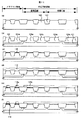
まず、面方位(100)のp型Si基板101に、各メモリセル及び周辺回路MOSトランジスタを分離する浅溝素子分離領域102を形成した(図1(a))。
【0031】
次いで、イオン打込み法によりPウェル領域104a,104b,104c及びNウェル領域105a,105b更にウェル間の分離領域103を形成した(図1(b))。
【0032】
次に、メモリセルのトンネル絶縁膜となるSiO2膜106を熱酸化法により9nm形成した(図1(c))。
【0033】
次に、浮遊ゲートとなるリンをドーピングした多結晶Si膜107を150nm堆積した(図1(d))。
【0034】
続いて、リソグラフィとドライエッチング技術を用いて多結晶Si膜107をパターニングした(多結晶Si膜107は107aとなる)。この際、周辺回路領域の多結晶Si膜107及びSiO2膜106は完全に除去した(図1(e))。
【0035】
次いで、SiH4とN2Oを原料ガスとした減圧化学気相成長法(LPCVD法)により、SiO2膜108を16nm堆積した。堆積温度は750℃である。その直後にSiO2膜108をNH3雰囲気中でアニールし、さらにウェット酸化を行なった(図1(f))。
【0036】
その後、リソグラフィ技術により周辺回路領域のうち高電圧部のみが被覆されるようなレジストパターンを作成し(図示せず)、フッ酸とアンモニアの混合水溶液によりメモリセル領域及び周辺回路領域のうち低電圧部に存在するSiO2膜108を除去した(SiO2膜108は108aとなる)(図2(a))。
【0037】
その後、再び、SiH4とN2Oを原料ガスとしたLPCVD法により、SiO2膜109を11nm堆積した。堆積温度は750℃である。その直後にSiO2膜109をNH3雰囲気中でアニールし、さらにウェット酸化を行なった(図2(b))。
【0038】
以上、図1(f)から図2(b)に示した工程により、メモリセル領域には11nmの多結晶Si層間絶縁膜(CVDSiO2膜109)が、周辺回路領域の低電圧部には11nmのゲート酸化膜(CVDSiO2膜109)が、周辺回路領域の高電圧部には概ね27nmのゲート酸化膜(CVDSiO2膜108aとCVDSiO2膜109の積層膜)が形成される。ここで、CVDSiO2膜堆積後、NH3雰囲気中でアニールし、さらにウェット酸素を行なっているのは、E’センタと呼ばれる膜中の欠陥や水素原子を低減するためである。これにより絶縁膜のリーク電流を抑制するとともに、トラップを低減し、メモリセルの電荷保持特性の向上を図れる。更に、周辺回路MOSトランジスタの相互コンダクタンスを向上するためである。
【0039】
次に、メモリセルの制御ゲートと周辺回路のゲート電極となるリンをドーピングした多結晶Si膜110を堆積した(図2(c))。
【0040】
その後、リソグラフィとドライエッチング技術により多結晶Si膜110をパターニングし、メモリセルの制御ゲート(ワード線)110a及び周辺回路のゲート電極110bを形成した。続いて、図には示していないが、メモリセル領域のSiO2膜109及び多結晶Si膜107aをエッチングし、浮遊ゲートを形成した(SiO2膜109及び多結晶Si膜107aはそれぞれ109a、107bとなる(図2(d))。
【0041】
次に、イオン打込み法により、メモリセル及び周辺回路MOSトランジスタのソース/ドレイン領域111b,111c,112a,112b(メモリセルのソース/ドレイン領域は図示せず)を形成した(図2(e))。
【0042】
その後、図には示していないが、層間絶縁膜を堆積した後、この層間絶縁膜にワード線110a,周辺回路領域MOSトランジスタのゲート電極110b及びソース/ドレイン領域112,111に至るコンタクト孔を形成し、次に、金属膜を堆積し、これを加工して電極とし、不揮発性半導体記憶装置を完成した。
【0043】
図3は本発明の方法により形成した周辺回路領域の高電圧部MOSトランジスタのゲート電圧とドレイン電流の関係を示したものである。同図には比較のため、上記MOSトランジスタのゲート酸化膜を熱酸化法により形成した場合の結果も合わせて示した。いずれもゲート酸化膜厚は28nmである。熱酸化法を用いた従来技術では電流−電圧特性にいわゆるキンクと呼ばれるこぶが観察され、特性劣化が認められた。これに対し、本発明の窒素を添加したCVDSiO2膜を用いた場合には、良好な電流−電圧特性が得られた。
【0044】
図4は、本発明の方法及び従来技術である熱酸化法により形成した周辺回路領域高電圧部MOSトランジスタのゲート酸化膜の絶縁耐圧を測定した結果である。同図より、熱酸化膜に代えて窒素を添加したCVDSiO2膜をゲート酸化膜に用いることにより、その絶縁耐圧が向上することが明らかとなった。
【0045】
上記、図3及び図4で示した従来技術と本発明の特性差を明らかにするために、走査型電子顕微鏡を用いて高電圧部MOSトランジスタの断面構造を観察した。その結果を図5に示す。熱酸化膜200をゲート酸化膜に用いた従来技術の場合には、Eで示した浅溝分離領域と接する部分のゲート酸化膜厚がアクティブ領域中央に比べ著しく薄くなっていた(図5(a))。この局所的なゲート酸化膜の薄膜化により電流−電圧特性の劣化や絶縁耐圧の低下が生じたことが判明した。これに対し、窒素を添加したCVDSiO2膜を用いた本発明の場合には、熱酸化膜で見られたような浅溝分離領域付近でのゲート酸化膜の薄膜化が抑制された(図5(b))。このため、良好な特性が得られたことが明かとなった。
【0046】
なお、周辺回路MOSトランジスタにCVDSiO2膜を適用した場合、同膜への窒素添加は極めて重要である。図1から図2で示した不揮発性半導体装置の製造において、CVDSiO2膜108及び109の形成の際、アンモニア中でのアニールを行なわず、窒素を添加しなかった場合には、窒素を添加した場合に比べて周辺回路低電圧部及び高電圧部いずれのMOSトランジスタにおいても相互コンダクタンスの大幅な低下がみられた。また、ゲート酸化膜の絶縁耐圧も低下した。
【0047】
本実施例1においては、メモリセルの多結晶Si層間絶縁膜と周辺回路低電圧部MOSトランジスタのゲート酸化膜を全く同一の工程により形成している。このため、メモリセルのトンネル酸化膜を含めて4種類あるゲート絶縁膜を3種類の膜で形成することが可能である。従って、ゲート絶縁膜をそれぞれ単独に形成する場合に比べて製造工程数の削減が可能となる。
【0048】
図6は、図1及び図2で示した方法により作成した不揮発性半導体記憶装置のメモリセルの多結晶Si層間絶縁膜,周辺回路領域の低電圧部及び高電圧部MOSトランジスタのゲート酸化膜中の窒素分布を二次イオン質量分析計により測定した結果である。多結晶Si層間絶縁膜と低電圧部MOSトランジスタのゲート酸化膜を同一工程にて形成しているにもかかわらず、窒素濃度は多結晶Si層間絶縁膜が一番高く、次いで低電圧部ゲート酸化膜、高電圧部ゲート酸化膜の順となっている。これはSiO2膜中への窒素の添加量が下地Si層の不純物濃度の増大とともに増加するためである。
【0049】
なお、周辺回路領域のMOSトランジスタのゲート酸化膜を、ともにCVD法により形成したメモリセルのトンネル酸化膜と多結晶Si層間絶縁膜の積層膜で形成する技術が特開平11−87545に示されている。しかし、同方法では周辺回路トランジスタのゲート酸化膜の膜厚がメモリセルの2つの酸化膜の膜厚の和で決まってしまうため、膜厚の設定に自由度がないという問題があった。また、浮遊ゲートのパターニングの際ダメージの入ったトンネル酸化膜をそのまま周辺回路トランジスタのゲート酸化膜に用いているため、膜特性の劣化が課題であった。本実施例の方法によれば、周辺回路高電圧部MOSトランジスタのゲート酸化膜厚はSiO2膜108の膜厚を変えることにより任意に設定できるという利点がある。また、SiO2膜108のパターニングにはウェットエッチングを用いているので、ダメージによる膜特性の劣化がない。
【0050】
以上、本実施例1によれば、不揮発性半導体記憶装置の周辺回路領域MOSトランジスタの特性及び信頼性が向上するという効果がある。なお、周辺回路領域MOSトランジスタの特性及び信頼性の向上という観点からいえば、周辺回路領域MOSトランジスタのゲート絶縁膜の全部(低電圧部)又は一部(高電圧部)がメモリセルの多結晶Si層間絶縁膜と同一工程で形成されることは必須要件ではなく、周辺回路領域MOSトランジスタのゲート絶縁膜が堆積により形成された絶縁膜、例えばCVDSiO2膜であればよい。また、本実施例によれば、メモリセルの微細化及び動作電圧の低減が可能な不揮発性半導体記憶装置の製造プロセスが構築できる。さらに、工程数を増大することなく周辺回路MOSトランジスタのゲート酸化膜を2種類とすることができる。
【0051】
(実施例2)
本実施例2では、不揮発性半導体記憶装置のメモリセルの多結晶Si層間絶縁膜と周辺回路領域MOSトランジスタのゲート酸化膜を窒素を添加したCVDSiO2膜とし、これを同時に形成することにより、周辺回路領域MOSトランジスタの特性向上とメモリセルの微細化,動作電圧の低減、及び製造工程の簡略化を図った別の例について説明する。
【0052】
本実施例の不揮発性半導体記憶装置の作成手順を図7から図9に示す。なお、図7から図9はメモリセルのワード線に平行で、周辺回路領域MOSトランジスタのゲート線に垂直な断面図である。実施例1との違いは、メモリセル領域においてセル間を分離する素子分離領域が存在しないこと、また、隣接するメモリセルのソースとドレインを共有する、いわゆる仮想接地型のメモリセルであること、更に、メモリセルに浮遊ゲート,制御ゲートとは異なる第3のゲート114a(以下、補助ゲートと称す)を有する点である。この補助ゲート114aは浮遊ゲート107b間に埋込まれて存在し、書込みの際のホットエレクトロンの注入効率を増大する機能を有する。また、補助ゲートに0Vを印加することにより隣接するメモリセル間を分離する機能も果たしている。このため、実施例1の通常のNOR型セルに比べ、メモリセル面積の縮小が可能である。また、複数のセルで同時に書込み動作を行なうことができ、書込みスループットの向上が図れる。従って大容量化に好適である。
【0053】
製造方法は以下の通りである。
【0054】
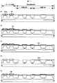
まず、面方位(100)のp型Si基板101に、周辺回路領域のMOSトランジスタを分離する浅溝素子分離領域102を形成した(図7(a))。
【0055】
次いで、イオン打込み法によりPウェル領域104a,104b,104c及びNウェル領域105a,105b更にウェル間の分離領域103を形成した(図7(b))。
【0056】
次に、補助ゲート下のゲート酸化膜となるSiO2膜113を熱酸化法により9nm形成した(図7(c))。
【0057】
次に、補助ゲートとなるリンをドーピングした多結晶Si膜114を60nm、SiO2膜115を150nm堆積した(図7(d))。
【0058】
続いて、リソグラフィとドライエッチング技術を用いて、厚いSiO2膜115及び多結晶Si膜114をパターニングした(SiO2膜115及び多結晶Si膜114はそれぞれ115a及び114aとなる)。この際、周辺回路領域のSiO2膜115及び多結晶Si膜114は完全に除去した(図7(e))。
【0059】
次に、リソグラフィ技術によりメモリセル領域のみが露出するレジストパターンを形成した後(図示せず)、斜めイオン打込み法によりメモリセルのソース/ドレイン拡散層領域116を形成した(図7(f))。
【0060】
次いで、周辺回路領域に残存していたゲート酸化膜114を除去した後(図示せず)、メモリセルのトンネル酸化膜となるSiO2膜106を9nm形成した(図8(a))。
【0061】
次に、浮遊ゲートとなるリンをドーピングした多結晶Si膜107を補助ゲートパターン間の隙間が埋まらないように、例えば50nm堆積した(図8(b))。
【0062】
次に、ホトレジスト117を補助ゲートパターン間の隙間が完全に埋まるように塗布し(図示せず)、これをエッチバックして、補助ゲートパターン間の隙間に残した(図8(c))。
【0063】
次に、エッチバック法によりホトレジスト117に被われていない部分に存在する多結晶Si膜107を除去した(多結晶Si膜107は107aとなる)。エッチング量は多結晶Si膜107の膜厚より若干大きな値とした(図8(d))。本工程により1回の膜形成で立体構造を有する浮遊ゲートパターンが形成できる。
【0064】
次に、アッシング法により多結晶Si膜107a上に残存するホトレジスト117を除去した(図8(e))。
【0065】
次に、SiH4とN2Oを原料ガスとした減圧化学気相成長法(LPCVD法)により、SiO2膜108を16nm堆積した。堆積温度は750℃である。その直後にSiO2膜108をNH3雰囲気中でアニールし、さらにウェット酸化を行なった(図8(f))。
【0066】
その後、リソグラフィ技術により周辺回路領域のうち高電圧部のみが被服されるようなレジストパターンを作成し(図示せず)、フッ酸とアンモニアの混合水溶液によりメモリセル領域及び周辺回路領域のうち低電圧部に存在するSiO2膜108を除去した(SiO2膜108は108aとなる)(図9(a))。
【0067】
その後、再び、SiH4とN2Oを原料ガスとしたLPCVD法により、SiO2膜109を11nm堆積した。堆積温度は750℃である。その直後にSiO2膜109をNH3雰囲気中でアニールし、さらにウェット酸化を行なった(図9(b))。
【0068】
以上、実施例1と同様、図8(f)から図9(b)に示した工程により、メモリセル領域には11nmの多結晶Si層間絶縁膜(CVDSiO2膜109)が、周辺回路領域の低電圧部には11nmのゲート酸化膜(CVDSiO2膜109)が、周辺回路領域の高電圧部には概ね27nmのゲート酸化膜(CVDSiO2膜108aとCVDSiO2膜109)が形成される。
【0069】
次に、メモリセルの制御ゲートと周辺回路のゲート電極となるリンをドーピングした多結晶Si膜110を堆積した(図9(c))。
【0070】
その後、リソグラフィとドライエッチング技術により多結晶Si膜110をパターニングし、メモリセルの制御ゲート(ワード線)110a及び周辺回路のゲート電極110bを形成した。続いて、図には示していないが、メモリセル領域のSiO2膜109及び多結晶Si膜107aをエッチングし、浮遊ゲートを形成した(SiO2膜109及び多結晶Si膜107aはそれぞれ109a、107bとなる(図9(d))。
【0071】
次に、周辺回路MOSトランジスタのソース/ドレイン領域111b,111c,112a,112bを形成した(図9(e))。
【0072】
その後、図には示していないが、層間絶縁膜を堆積した後、この層間絶縁膜にワード線110a,周辺MOSトランジスタのゲート電極110b及びソース/ドレイン領域112,111に至るコンタクト孔を形成し、次に、金属膜を堆積し、これを加工して電極とし、不揮発性半導体記憶装置を完成した。
【0073】
本実施例2によれば、実施例1と同様、不揮発性半導体記憶装置の周辺回路MOSトランジスタの特性及び信頼性が向上した。また、実施例1に比べメモリセルの微細化及び動作電圧の低減が可能であった。さらに工程数を増大することなく周辺回路MOSトランジスタのゲート酸化膜を2種類とすることができた。
【0074】
(実施例3)
本実施例3では、不揮発性半導体記憶装置のメモリセルの多結晶Si層間絶縁膜と周辺回路MOSトランジスタのゲート酸化膜とを窒素を添加したCVDSiO2膜とし、これを同時に形成することにより、周辺回路MOSトランジスタの特性向上とメモリセルの微細化,動作電圧の低減及び製造工程の簡略化を図った更に別の例について説明する。
【0075】
本実施例の不揮発性半導体記憶装置の作成手順を図10から図12に示す。なお、図10から図12はメモリセルのワード線に平行で、周辺回路MOSトランジスタのゲート線に垂直な断面図である。実施例1との違いは、メモリセルアレイがソース線を分離し、セルを並列に配置したAND型と呼ばれる構造になっている点である。
【0076】
製造方法は以下の通りである。
【0077】
まず、面方位(100)のp型Si基板101に、周辺回路MOSトランジスタを分離する浅溝素子分離領域102を形成した(図10(a))。
【0078】
次いで、イオン打込み法によりPウェル領域104a,104b,104c及びNウェル領域105a,105b更にウェル間の分離領域103を形成した(図10(b))。
【0079】
次いで、メモリセルのトンネル酸化膜となるSiO2膜106を熱酸化法により9nm形成した(図10(c))。
【0080】
次に、1層目の浮遊ゲートとなるリンをドーピングした多結晶Si膜118を100nm堆積した(図10(d))。
【0081】
続いて、リソグラフィとドライエッチング技術を用いて、多結晶Si膜118をパターニングした。この際、周辺回路領域の多結晶Si膜118はそのまま残すようなパターンとした(多結晶Si膜118はメモリセル領域が118a、周辺回路領域が118bとなる)(図10(e))。
【0082】
次に、イオン打込み法により、メモリセルのソース/ドレイン拡散層領域116を形成した(図10(f))。
【0083】
次いで、SiO2膜119を1層目の浮遊ゲート間を完全に埋込むよう、例えば400堆積した(図11(a))。
【0084】
その後、化学的機械研磨法(CMP法)により、SiO2膜119を研磨し、1層目の浮遊ゲートパターン118a及び118bを露出させた(多結晶Si膜118a及び118bはそれぞれ118c及び118dとなる)(図11(b))。
【0085】
次に、2層目の浮遊ゲートとなるリンをドーピングした多結晶Si膜120を例えば50nm堆積した(図11(c))。
【0086】
次に、リソグラフィとドライエッチング技術を用いて、多結晶Si膜120をパターニングした(多結晶Si膜120は120aとなる)。この際、周辺回路領域の多結晶Si膜120及びその下に存在していた多結晶Si膜118dは完全に除去した(図11(d))。本実施例の不揮発性半導体装置のメモリセルにおいては、多結晶Si膜118c及び120aは電気的に接続されており、この2層で浮遊ゲートが形成される。
【0087】
次に、SiH4とN2Oを原料ガスとした減圧化学気相成長法(LPCVD法)により、SiO2膜108を16nm堆積した。堆積温度は750℃である。その直後にSiO2膜108をNH3雰囲気中でアニールし、さらにウェット酸化を行なった(図11(e))。
【0088】
その後、リソグラフィ技術により周辺回路領域のうち高電圧部のみが被服されるようなレジストパターンを作成し(図示せず)、フッ酸とアンモニアの混合水溶液によりメモリセル領域及び周辺回路領域のうち低電圧部に存在するSiO2膜108を除去した(SiO2膜108は108aとなる)(図12(a))。
【0089】
その後、再び、SiH4とN2Oを原料ガスとしたLPCVD法により、SiO2膜109を11nm堆積した。堆積温度は750℃である。その直後にSiO2膜109をNH3雰囲気中でアニールし、さらにウェット酸化を行なった(図12(b))。
【0090】
以上、実施例1と同様、図11(e)から図12(b)に示した工程により、メモリセル領域には11nmの多結晶Si層間絶縁膜(CVDSiO2膜109)が、周辺回路領域の低電圧部には11nmのゲート酸化膜(CVDSiO2膜109)が、周辺回路領域の高電圧部には概ね27nmのゲート酸化膜(CVDSiO2膜108aとCVDSiO2膜109)が形成される。
【0091】
次に、メモリセルの制御ゲートと周辺回路領域MOSトランジスタのゲート電極となるリンをドーピングした多結晶Si膜110を堆積した(図11(c))。
【0092】
その後、リソグラフィとドライエッチング技術により多結晶Si膜110をパターニングし、メモリセルの制御ゲート(ワード線)110a及び周辺回路のゲート電極110bを形成した。続いて、図には示していないが、メモリセル領域のSiO2膜109及び多結晶Si膜120a,118cをエッチングし、浮遊ゲートを形成した(SiO2膜109及び多結晶Si膜120a,118cはそれぞれ109a及び120b,118dとなる(図11(d))。
【0093】
次に、周辺回路領域MOSトランジスタのソース/ドレイン領域111b,111c,112a,112bを形成した(図11(e))。
【0094】
その後、図には示していないが、層間絶縁膜を堆積した後、この層間絶縁膜にワード線110a,周辺回路領域MOSトランジスタのゲート電極110b及びソース/ドレイン領域112,111に至るコンタクト孔を形成し、次に、金属膜を堆積し、これを加工して電極とし、不揮発性半導体記憶装置を完成した。
【0095】
本実施例3によれば、実施例1と同様、不揮発性半導体記憶装置の周辺回路MOSトランジスタの特性及び信頼性が向上した。また、メモリセルの微細化及び動作電圧の低減が可能であった。さらに、工程数を増大することなく周辺回路MOSトランジスタのゲート酸化膜を2種類とすることができた。
【0096】
(実施例4)
本実例4では、実施例1とは異なり、周辺回路領域高電圧部のMOSトランジスタのゲート酸化膜の一部を、窒素を添加したCVDSiO2膜に代えて、薄い熱酸化膜を用いた例について述べる。
【0097】
本実施例の不揮発性半導体記憶装置の作成手順を図13に示す。本実施例の不揮発性半導体記憶装置の浮遊ゲート107aを形成するまでの工程は、実施例1の図1(a)から図1(e)と同一であり、ここでは省略した。
【0098】
図1(e)に示したような浮遊ゲートパターンを形成した後、SiH4とN2Oを原料ガスとしたLPCVD法により、SiO2膜121を4nm堆積した。(図13(a))。
【0099】
次に、LPCVD法によりSi3N4膜122を10nm堆積し、その後、リソグラフィ技術により周辺回路領域のうち高電圧部のみが露出するようなレジストパターンを作成し(以上図示せず)、ドライエッチングにより高電圧部に存在するSi3N4膜122を除去した(図13(b))。
【0100】
次に、高電圧部に存在するSiO2膜121をフッ酸水溶液により除去した後(図示せず)、熱酸化法により、Si3N4膜122に被われていない周辺回路高電圧部にのみ選択的にSiO2膜123を成長させた。酸化膜厚は16nmである。上記Si3N4膜122は耐酸化性を有するため、Si3N4膜122に被われているメモリセル領域及び周辺回路領域のうち低電圧部では酸化反応は進行しない(図13(c))。
【0101】
その後、熱リン酸水溶液によりSi3N4膜122を除去した後、フッ酸水溶液によりメモリセル部及び周辺回路低電圧部に存在するSiO2膜121を除去した。この際、周辺回路高電圧部のSiO2膜123もその表面が若干エッチングされ、膜厚が14nmに減少する(SiO2膜123は123aとなる)(図13(d))。
【0102】
その後、SiH4とN2Oを原料ガスとしたLPCVD法により、SiO2膜109を11nm堆積した。堆積温度は750℃である。その直後にSiO2膜109をNH3雰囲気中でアニールし、さらにウェット酸化を行なった(図13(e))。
【0103】
以上の工程により、メモリセル領域には11nmの多結晶Si層間絶縁膜(CVDSiO2膜109)が、周辺回路領域の低電圧部には11nmのゲート酸化膜(CVDSiO2膜109)が、周辺回路領域の高電圧部には概ね25nmのゲート酸化膜(熱酸化SiO2膜123aとCVDSiO2膜109)が形成される。
【0104】
その後、実施例1の図2(c)から図2(e)と同様の工程を行ない、不揮発性半導体記憶装置を完成した。
【0105】
本実施例4においては、熱酸化法を用いても実施例1と同一のマスク枚数で不揮発性半導体記憶装置が作成可能であった。また、実施例1に比べ周辺回路高電圧部のMOSトランジスタのゲート酸化膜/Si基板界面の特性が向上し、コンダクタンスが向上した。
【0106】
なお、本実施例4においては、周辺回路高電圧部のMOSトランジスタのゲート酸化膜を、熱酸化膜と窒素を添加したCVDSiO2膜により形成している。熱酸化を行なったため、図5(a)で示したような浅溝分離領域に接する部分で若干のゲート酸化膜厚の減少が観察された。しかしながら、酸化膜厚が14nmと従来技術に比べ薄かったため、図3及び図4で示したMOSトランジスタの電流-電圧特性、及び絶縁耐圧の劣化は実用上問題ないレベルであった。
【0107】
(実施例5)
実施例4で述べたように、周辺回路MOSトランジスタのゲート酸化膜に熱酸化膜を用いても、その酸化膜厚が薄い場合には、浅溝分離領域に接する部分での酸化膜の薄膜化の程度は小さく、MOS特性の劣化を実用上問題ないレベルとすることが可能である。そこで、本実施例では、周辺回路領域のうち低電圧部MOSトランジスタのゲート酸化膜に薄膜化した熱酸化膜を使用し、不揮発性半導体記憶装置の性能向上を図った例について述べる。
【0108】
本実施例の不揮発性半導体記憶装置の作成手順を図14から図15に示す。ウェル領域を形成するまでの工程は実施例1の図1(a)から図1(b)と同一であり、ここでは省略した。
【0109】
実施例1の図1(a)から図1(b)に示したように、素子分離領域及びウェル領域を形成した後、メモリセルのトンネル絶縁膜となるSiO2膜106を熱酸化法により9nm形成した(図14(a))。
【0110】
次に、リソグラフィ技術を用いて、周辺回路領域低電圧部のみが露出するようなレジストパターンを形成した後(図示せず)、周辺回路領域低電圧部のSiO2膜106をフッ酸とアンモニアの混合水溶液により除去した(図14(b))。
【0111】
次に、周辺回路領域低電圧部のMOSトランジスタのゲート酸化膜となるSiO2膜124を熱酸化法により5nm形成した(図14(c))。
【0112】
次に、浮遊ゲートとなるリンをドーピングした多結晶Si膜107を150nm堆積した(図14(d))。
【0113】
続いて、リソグラフィとドライエッチング技術を用いて多結晶Si膜107をパターニングした。この際、周辺回路領域の多結晶Si膜107は、高電圧部では完全に除去し、低電圧部ではその全面が被われるように残した(多結晶Si膜107は107a,107cとなる)(図14(e))。
【0114】
次いで、SiH4とN2Oを原料ガスとした減圧化学気相成長法(LPCVD法)により、SiO2膜108を16nm堆積した。堆積温度は750℃である。その直後にSiO2膜108をNH3雰囲気中でアニールし、さらにウェット酸化を行なった(図14(f))。
【0115】
その後、リソグラフィ技術により周辺回路領域のうち高電圧部のみのSiO2膜108が被覆されるようなレジストパターンを作成し(図示せず)、フッ酸とアンモニアの混合水溶液によりメモリセル領域及び周辺回路領域のうち低電圧部に存在するSiO2膜108を除去した(SiO2膜108は108aとなる)(図15(a))。
【0116】
その後、再び、SiH4とN2Oを原料ガスとしたLPCVD法により、SiO2膜109を11nm堆積した。堆積温度は750℃である。その直後にSiO2膜109をNH3雰囲気中でアニールし、さらにウェット酸化を行なった(図15(b))。
【0117】
以上の工程により、メモリセル領域には11nmの多結晶Si層間絶縁膜(CVDSiO2膜109)が、周辺回路領域の低電圧部には5nmのゲート酸化膜(熱酸化SiO2膜124)が、周辺回路領域の高電圧部には概ね27nmのゲート酸化膜(CVDSiO2膜108aとCVDSiO2膜109)が形成される。
【0118】
次に、メモリセルの制御ゲートと周辺回路のゲート電極となるリンをドーピングした多結晶Si膜110を堆積した(図15(c))。
【0119】
その後、リソグラフィとドライエッチング技術により多結晶Si膜110をパターニングし、メモリセルの制御ゲート(ワード線)110a及び周辺回路のゲート電極110bを形成した。続いて図には示していないが、メモリセル領域及び周辺回路領域低電圧部MOSトランジスタのSiO2膜109及び多結晶Si膜107a,107cをエッチングした。これにより浮遊ゲートが完成した(SiO2膜109及び多結晶Si膜107a,107cはそれぞれ109a及び107b,107dとなる)。この際、周辺回路領域低電圧部の多結晶Si膜107dの一部が露出するようにパターニングした(図15(d))。
【0120】
次に、イオン打込み法により、メモリセル及び周辺回路MOSトランジスタのソース/ドレイン領域111b,111c,112a,112b(メモリセルのソース/ドレイン領域は図示せず)を形成した後、図には示していないが、層間絶縁膜を堆積し、この層間絶縁膜に多結晶Si膜110aより成るワード線、周辺回路領域MOSトランジスタの多結晶Si膜110bより成るゲート電極及びソース/ドレイン領域112,111に至るコンタクト孔を形成した。次に、金属膜を堆積し、これを加工して電極とした。この際、周辺回路領域低電圧部においては、多結晶Si膜110b及び107dが電気的に接続されるよう、コンタクト孔と金属電極を配置した。これにより周辺回路領域低電圧部のMOSトランジスタにおいては、多結晶Si膜110bに印加された電圧は多結晶Si膜107dにも印加される。以上の工程により不揮発性半導体記憶装置を完成した(図15(e))。
【0121】
本実施例5により形成した不揮発性半導体記憶装置は、実施例1と同様、不揮発性半導体記憶装置の周辺回路MOSトランジスタの特性及び信頼性が向上した。また、メモリセルの微細化及び動作電圧の低減が可能であった。さらに、工程数を増大することなく周辺回路MOSトランジスタのゲート酸化膜を2種類とすることができた。更に、実施例1に比べ、周辺回路低電圧部の高速動作が可能となり、書換え及び読出し速度の向上が図れた。
【0122】
(実施例6)
本実施例6では、周辺回路領域高電圧部MOSトランジスタのゲート酸化膜に薄膜化した熱酸化膜と窒素を添加したCVDSiO2の積層膜を使用し、不揮発性半導体記憶装置の性能向上を図った別の例について述べる。
【0123】
本実施例6の不揮発性半導体記憶装置の作成手順を図16から図17に示す。ウェル領域を形成するまでの工程は実施例1の図1(a)から図1(b)と同一であり、ここでは省略した。
【0124】
実施例1の図1(a)から図1(b)に示したように、素子分離領域及びウェル領域を形成した後、SiH4とN2Oを原料ガスとした減圧化学気相成長法(LPCVD法)により、SiO2膜125を20nm堆積した。堆積温度は750℃である。その直後にSiO2膜108をNH3雰囲気中でアニールし、さらにウェット酸化を行なった(図16(a))。
【0125】
次に、リソグラフィ技術を用いて、周辺回路領域高電圧部のみが被覆されるようなレジストパターンを形成した後(図示せず)、メモリセル領域及び周辺回路領域低電圧部のSiO2膜125をフッ酸とアンモニアの混合水溶液により除去した(SiO2膜125は125aとなる)(図16(b))。
【0126】
次に、メモリセルのトンネル絶縁膜及び周辺回路領域低電圧部のゲート酸化膜となるSiO2膜126を熱酸化法により9nm形成した。この際、周辺回路領域高電圧部でもメモリセル領域程ではないが酸化膜126aが成長する。
【0127】
以上の工程により、メモリセル領域には9nmのトンネル絶縁膜(熱酸化SiO2膜126)が、周辺回路領域の低電圧部には9nmのゲート酸化膜(熱酸化SiO2膜126)が、周辺回路領域の高電圧部には概ね27nmのゲート酸化膜(熱酸化SiO2膜126aとCVDSiO2膜125a)が形成される。(図16(c))。
【0128】
次に、浮遊ゲートとなるリンをドーピングした多結晶Si膜107を150nm堆積した(図16(d))。
【0129】
続いて、リソグラフィとドライエッチング技術を用いて多結晶Si膜107をパターニングした。この際、周辺回路領域の多結晶Si膜107はその全面が被われるように残した(多結晶Si膜107はメモリセル領域が107a、周辺回路領域が107eとなる)(図16(e))。
【0130】
次いで、SiH4とN2Oを原料ガスとしたLPCVD法により、多結晶Si層間絶縁膜となるSiO2膜109を11nm堆積した。堆積温度は750℃である。その直後にSiO2膜109をNH3雰囲気中でアニールし、さらにウェット酸化を行なった(図17(a))。
【0131】
次に、メモリセルの制御ゲートと周辺回路のゲート電極となるリンをドーピングした多結晶Si膜110を堆積した(図17(b))。
【0132】
その後、リソグラフィとドライエッチング技術により多結晶Si膜110をパターニングし、メモリセルの制御ゲート(ワード線)110a及び周辺回路のゲート電極110bを形成した。続いて図には示していないが、メモリセル領域及び周辺回路領域MOSトランジスタのSiO2膜109及び多結晶Si膜107a,107eをエッチングした。これにより、浮遊ゲートが完成した(SiO2膜109及び多結晶Si膜107a,107cはそれぞれ109a及び107b、107fとなる)。この際、周辺回路領域の多結晶Si膜107dの一部が露出するようにパターニングした(図17(c))。
【0133】
次に、イオン打込み法により、メモリセル及び周辺回路領域MOSトランジスタのソース/ドレイン領域111b,111c,112a,112b(メモリセルのソース/ドレイン領域は図示せず)を形成した後、図には示していないが、層間絶縁膜を堆積し、この層間絶縁膜に多結晶Si膜110aより成るワード線、周辺回路領域MOSトランジスタの多結晶Si膜110bより成るゲート電極及びソース/ドレイン領域112,111に至るコンタクト孔を形成した。次に、金属膜を堆積し、これを加工して電極とした。この際、周辺回路領域においては、多結晶Si膜110b及び107dが電気的に接続されるよう、コンタクト孔と金属電極を配置した。これにより周辺回路領域のMOSトランジスタにおいては、多結晶Si膜110bに印加された電圧は多結晶Si膜107dにも印加される。以上の工程により不揮発性半導体記憶装置を完成した。(図17(d))
本実施例により形成した不揮発性半導体記憶装置は、実施例1と同様、不揮発性半導体記憶装置の周辺回路領域MOSトランジスタの特性及び信頼性が向上した。また、メモリセルの微細化及び動作電圧の低減が可能であった。さらに、工程数を増大することなく周辺回路MOSトランジスタのゲート酸化膜を2種類とすることができた。更に、実施例1に比べ、周辺回路低電圧部の高速動作が可能となり、書換え及び読出し速度の向上が図れた。以上に詳述した各実施例においては、不揮発性半導体装置のメモリセルとしてNOR型,補助ゲートを有するセル,AND型を例に用いて説明したが、その他のメモリセル、例えばNAND型やスプリットゲート型のセル、あるいは消去ゲートを有するメモリセルを用いても同様の効果が得られる。
【0134】
また、不揮発性半導体記憶装置とマイクロコントローラを1つのチップに混載した製品に適用しても、同様の効果が得られる。
【0135】
【発明の効果】
本発明によれば、不揮発性半導体記憶装置の周辺回路領域MOSトランジスタのゲート酸化膜の信頼性が向上し、トランジスタ特性を向上できる。
また、不揮発性半導体記憶装置の微細化、低電圧化が図られる。
更に、不揮発性半導体記憶装置の製造工程の簡略化を図ることができる。
【図面の簡単な説明】
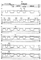
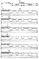
【図1】本発明の実施例1を示す断面概略図(1)。
【図2】本発明の実施例1を示す断面概略図(2)。
【図3】ゲート電圧とゲート電流の関係を示す図。
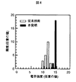
【図4】ゲート酸化膜の絶縁耐圧の分布を示す図。
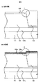
【図5】浅溝分離領域近傍のゲート酸化膜形状を示す図。
【図6】SiO2膜中の窒素原子濃度分布を示す図。
【図7】本発明の実施例2を示す断面概略図(1)。
【図8】本発明の実施例2を示す断面概略図(2)。
【図9】本発明の実施例2を示す断面概略図(3)。
【図10】本発明の実施例3を示す断面概略図(1)。
【図11】本発明の実施例3を示す断面概略図(2)。
【図12】本発明の実施例3を示す断面概略図(3)。
【図13】本発明の実施例4を示す断面概略図。
【図14】本発明の実施例5を示す断面概略図(1)。
【図15】本発明の実施例5を示す断面概略図(2)。
【図16】本発明の実施例6を示す断面概略図(1)。
【図17】本発明の実施例6を示す断面概略図(2)。
【図18】従来技術を示す断面概略図。
【符号の説明】
101…Si基板、102…浅溝素子分離領域、103…ウェル間分離領域、104a,104b,104c…Pウェル、105a,105b…Nウェル、106…熱酸化膜、107,107a,107b,107c,107d,107e,107f…リンをドーピングした多結晶Si膜、108,108a,109,109a…窒素原子を添加したSiO2膜、110,110a,110b…リンをドーピングした多結晶Si膜、111a,111b,111c…N型ソース/ドレイン領域、112a,112b…P型ソース/ドレイン領域、113…熱酸化膜、114,114a…リンをドーピングした多結晶Si膜、115,115a…SiO2膜、116…ソース/ドレイン領域、117…ホトレジスト、118,118a,118b,118c,118d,118e…リンをドーピングした多結晶Si膜、119,119a…SiO2膜、120,120a,120b…リンをドーピングした多結晶Si膜、121…SiO2膜、122…Si3N4膜、123,123a…熱酸化膜、124,124a…熱酸化膜、125,125a…窒素原子を添加したSiO2膜、126,126a…熱酸化膜、200…ゲート酸化膜、201…Si基板、202…素子分離用酸化膜、203…ウェル間分離領域、204a,204b…Pウェル、205…Nウェル、206…熱酸化膜、207…リンをドーピングした多結晶Si膜、208…ONO多結晶Si層間絶縁膜、209…リンをドーピングした多結晶Si膜、210…熱酸化膜、211…リンをドーピングした多結晶Si膜、212a,212b…ソース/ドレイン領域、M…メモリセル、P,P’…MOSトランジスタ。[0001]
BACKGROUND OF THE INVENTION
The present invention relates to a nonvolatile semiconductor memory device and a method for manufacturing the same, and to a technique for miniaturization, low voltage operation, high reliability, and simplification of the manufacturing process.
[0002]
[Prior art]
Flash memory, which is representative of non-volatile semiconductor memory devices, is excellent in portability and impact resistance, and can be erased collectively on-board, making it a memory for small portable information devices such as mobile phones and digital cameras. The market is expanding rapidly.
[0003]
For example, as shown in FIG. 18, the flash memory is usually a MOS type that constitutes a memory cell M for storing information and a peripheral circuit for selecting a bit for rewriting or reading or generating a necessary voltage inside the chip. It consists of a field effect transistor P.
[0004]
Among these, the memory cell M includes a silicon (Si)
[0005]
The peripheral circuit P includes a P well 204b and an N well 205 formed in the
[0006]
Each memory cell M and peripheral circuit transistor P are usually separated by an
[0007]
[Problems to be solved by the invention]
However, along with the increase in capacity of the nonvolatile semiconductor memory device described above, new problems have arisen in the peripheral circuit MOS transistor P and the memory cell M.
[0008]
The first point is deterioration of characteristics and reliability due to deterioration of the gate oxide film of the peripheral circuit MOS transistor.
[0009]
In a flash memory, a high voltage such as 18 V is applied to a word line at the time of writing / erasing. In such a peripheral circuit MOS transistor that handles a high voltage, a high breakdown voltage is achieved by increasing the gate oxide film thickness to, for example, about 25 nm. However, when the shallow trench isolation method is applied instead of the conventional selective oxidation method (LOCOS) for element isolation between peripheral MOS transistors for the miniaturization of elements, a thick gate oxide film of 25 nm is formed by the thermal oxidation method. As a result, a phenomenon occurred in which the gate oxide film thickness in contact with the shallow trench isolation region was significantly thinner than that in the active region. For this reason, there arises a problem that a so-called kink occurs in the current-voltage characteristics of the MOS transistor and the withstand voltage of the gate oxide film decreases.
[0010]
The second point is the thinning of the polycrystalline Si interlayer insulating film of the memory cell M which is indispensable for reducing the program voltage.
[0011]
The voltage Vfg applied to the floating gate during the flash memory rewrite operation is
Vfg = C2 ・ Vcg / (C1 + C2) (1)
Given in. Here, Vcg is a control gate applied voltage, and C1 and C2 are capacitances of the tunnel insulating film and the polycrystalline Si interlayer insulating film, respectively. In order to efficiently transmit the voltage applied to the control gate to the floating gate and reduce the program voltage, it is effective to increase C2, that is, to thin the polycrystalline Si interlayer insulating film. However, in a so-called ONO film in which a silicon nitride (Si3N4) film widely used in the past is sandwiched between SiO2 films, if the upper and lower SiO2 films are 5 nm or less, the charge accumulated in the floating gate is controlled by the control gate. There is a problem that a so-called retention failure that leaks into the surface becomes obvious. In addition, when an upper SiO2 film is formed to have a thickness of 5 nm, it is necessary to deposit a Si3N4 film of about 10 nm or more in order to prevent oxidation of the lower polycrystalline Si film. Therefore, the thickness of the ONO film is limited to about 15 nm in terms of oxide film.
[0012]
For this reason, Japanese Patent Application Laid-Open No. 9-238036 discloses a technique for reducing the program voltage by applying a single layer CVDSiO2 film added with nitrogen to the polycrystalline Si interlayer insulating film in place of the ONO film and reducing the thickness thereof. Has been.
[0013]
However, as is widely practiced in conventional flash memories, when a gate oxide film of a peripheral circuit MOS transistor is formed by thermal oxidation after forming a polycrystalline Si interlayer insulating film, unlike a ONO film, a single layer is formed. Since the CVDSiO2 film has no oxidation resistance, there is a problem that the floating gate polycrystalline Si doped with impurities at a high concentration is oxidized thickly. Accordingly, it has been necessary to develop a method for forming a gate oxide film of a peripheral circuit MOS transistor when a single-layer CVDSiO2 film is used as the memory cell polycrystalline Si interlayer insulating film.
[0014]
The third point is an increase in the number of processes.
[0015]
In the conventional flash memory, the
[0016]
The three problems described above are closely related to each other in terms of the formation of the interlayer insulating film of the memory cell and the gate oxide film of the peripheral circuit MOS transistor, and a new nonvolatile semiconductor memory device and a Development of the manufacturing method has been desired.
[0017]
An object of the present invention is to make the gate oxide film of a peripheral circuit region MOS transistor of a nonvolatile semiconductor memory device highly reliable and to improve transistor characteristics.
[0018]
Another object of the present invention is to provide a method for forming a polycrystalline Si interlayer insulating film and a gate oxide film of a peripheral circuit region MOS transistor corresponding to miniaturization and low voltage of a nonvolatile semiconductor memory device.
[0019]
Still another object of the present invention is to simplify the manufacturing process of a nonvolatile semiconductor memory device.
[0020]
[Means for Solving the Problems]
In order to solve the first problem, in the nonvolatile semiconductor memory device of the present invention, an insulating film formed by depositing a gate insulating film of a MOS field effect transistor constituting a peripheral circuit on a semiconductor substrate, for example, CVDSiO 2 It is formed by a film. As a result, even if the shallow groove isolation method is used for element isolation between the MOS field effect transistors, the gate oxide film thickness in the portion in contact with the shallow groove isolation region does not become thin, and the kink in the MOS field effect transistor characteristics can be obtained. In addition, it is possible to prevent a decrease in the withstand voltage of the gate oxide film. When the peripheral circuit is composed of a MOS field effect transistor having two or more types of gate insulating film thicknesses, the present invention is particularly applicable when applied to a MOS field effect transistor in a high voltage section having a thicker gate insulating film thickness. It is valid.
[0021]
Also, a gate insulating film of a MOS field effect transistor constituting a peripheral circuit is formed by depositing an insulating film obtained by thermally oxidizing the surface of a semiconductor substrate and an insulating film formed on the insulating film (for example, CVDSiO 2 Film), the thickness of the gate oxide film in contact with the shallow trench isolation region can be compensated by the deposited insulating film. When Similarly, kinks in the MOS field effect transistor characteristics can be prevented, and a decrease in the withstand voltage of the gate oxide film can be avoided. In this case, the deposited insulating film is thicker than the thermal oxide insulating film. Film thickness It is more preferable to increase the thickness in order to achieve the effect.
[0022]
In order to solve the second problem, in the method for manufacturing a nonvolatile semiconductor memory device of the present invention, an insulating film in which a gate insulating film of a MOS field effect transistor constituting a peripheral circuit is deposited on a semiconductor substrate, for example, It is formed by a CVD SiO2 film. As a result, even if the polycrystalline silicon interlayer insulating film is a CVDSiO2 film and the gate insulating film is formed after forming the polycrystalline silicon interlayer insulating film, the CVDSiO2 film of the polycrystalline silicon interlayer insulating film may be thickly oxidized. Can be avoided.
[0023]
Further, when all or part of the gate insulating film of the peripheral circuit is a thermal oxide film, the step of thermally oxidizing the semiconductor substrate surface must be performed before the step of forming the polycrystalline silicon interlayer insulating film. Thus, abnormal oxidation of the CVDSiO2 film, which is a polycrystalline silicon interlayer insulating film, can be prevented.
[0024]
In order to solve the third problem, in the nonvolatile semiconductor memory device and the manufacturing method thereof according to the present invention, an insulating film deposited for forming a polycrystalline silicon interlayer insulating film, for example, a CVD insulating film is used as a peripheral circuit. By using it as all or part of the gate insulating film of the MOS field effect transistor, the manufacturing process can be simplified.
[0025]
DETAILED DESCRIPTION OF THE INVENTION
Example 1
In the first embodiment, the polycrystalline Si interlayer insulating film of the memory cell of the nonvolatile semiconductor memory device and the gate oxide film of the peripheral circuit MOS transistor are formed as CVDSiO2 films to which nitrogen is added, and these are formed simultaneously, thereby forming the peripheral circuit. An example in which the characteristics of a MOS transistor is improved, the memory cell is miniaturized, the operating voltage is reduced, and the manufacturing process is simplified will be described.
[0026]
A procedure for producing the nonvolatile semiconductor memory device of this embodiment is shown in FIGS. A nonvolatile semiconductor memory device has a memory cell region in which a plurality of memory cells for storing information are arranged in a matrix, and a peripheral circuit that selects a bit for rewriting and reading, and generates a necessary voltage inside the chip. And a peripheral circuit region in which a plurality of MOS transistors for configuring the circuit are arranged.
[0027]
The peripheral circuit area is divided into a low voltage portion to which only a relatively small voltage such as a power supply voltage such as 3.3V is applied and a high voltage portion to which a high voltage necessary for rewriting such as 18V is applied. Both the low voltage portion and the high voltage portion are composed of a plurality of NMOS transistors and PMOS transistors formed on the
[0028]
1 and 2 are cross-sectional views parallel to the word line of the memory cell and perpendicular to the gate line of the MOS transistor of the peripheral circuit.
[0029]
The manufacturing method is as follows.
[0030]
First, a shallow groove
[0031]
Next, P well
[0032]
Next, a 9 nm
[0033]
Next, a
[0034]
Subsequently, the
[0035]
Next, a SiO 2
[0036]
Thereafter, a resist pattern is formed by a lithography technique so that only the high voltage portion of the peripheral circuit region is covered (not shown), and a low voltage is generated in the memory cell region and the peripheral circuit region with a mixed aqueous solution of hydrofluoric acid and ammonia. The
[0037]
Thereafter, an SiO 2
[0038]
As described above, by the steps shown in FIGS. 1F to 2B, the 11 nm polycrystalline Si interlayer insulating film (CVDSiO 2 film 109) is formed in the memory cell region, and the low voltage portion in the peripheral circuit region is formed by 11 nm. A gate oxide film (CVDSiO2 film 109) is formed on the high voltage portion in the peripheral circuit region with a gate oxide film (a laminated film of the
[0039]
Next, a
[0040]
Thereafter, the
[0041]
Next, the source /
[0042]
Thereafter, although not shown in the figure, after depositing an interlayer insulating film, contact holes reaching the
[0043]
FIG. 3 shows the relationship between the gate voltage and drain current of the high voltage MOS transistor in the peripheral circuit region formed by the method of the present invention. For comparison, the figure also shows the results when the gate oxide film of the MOS transistor is formed by a thermal oxidation method. In either case, the gate oxide film thickness is 28 nm. In the prior art using the thermal oxidation method, a hump called a kink was observed in the current-voltage characteristics, and characteristic deterioration was recognized. On the other hand, when the CVDSiO2 film to which nitrogen of the present invention was added was used, good current-voltage characteristics were obtained.
[0044]
FIG. 4 shows the results of measuring the withstand voltage of the gate oxide film of the peripheral circuit region high voltage MOS transistor formed by the method of the present invention and the conventional thermal oxidation method. From the figure, it has been clarified that the withstand voltage is improved by using a CVDSiO2 film to which nitrogen is added instead of the thermal oxide film as the gate oxide film.
[0045]
In order to clarify the characteristic difference between the prior art shown in FIGS. 3 and 4 and the present invention, the cross-sectional structure of the high voltage MOS transistor was observed using a scanning electron microscope. The result is shown in FIG. In the case of the prior art in which the
[0046]
When a CVD SiO 2 film is applied to the peripheral circuit MOS transistor, it is extremely important to add nitrogen to the film. In the manufacture of the nonvolatile semiconductor device shown in FIGS. 1 to 2, when
[0047]
In the first embodiment, the polycrystalline Si interlayer insulating film of the memory cell and the gate oxide film of the peripheral circuit low voltage part MOS transistor are formed in exactly the same process. For this reason, four types of gate insulating films including the tunnel oxide film of the memory cell can be formed of three types of films. Therefore, the number of manufacturing steps can be reduced as compared with the case where the gate insulating films are formed individually.
[0048]
FIG. 6 shows the polycrystalline Si interlayer insulating film of the memory cell of the nonvolatile semiconductor memory device produced by the method shown in FIGS. 1 and 2, the low voltage portion in the peripheral circuit region, and the gate oxide film of the high voltage portion MOS transistor. It is the result of having measured nitrogen distribution of this with the secondary ion mass spectrometer. Even though the polycrystalline Si interlayer insulating film and the gate oxide film of the low voltage part MOS transistor are formed in the same process, the nitrogen concentration is the highest in the polycrystalline Si interlayer insulating film, and then the low voltage part gate oxide film The order is the film, and the high-voltage gate oxide film. This is because the amount of nitrogen added to the SiO 2 film increases as the impurity concentration of the underlying Si layer increases.
[0049]
Japanese Laid-Open Patent Publication No. 11-87545 discloses a technique for forming a gate oxide film of a MOS transistor in a peripheral circuit region by a laminated film of a tunnel oxide film of a memory cell and a polycrystalline Si interlayer insulating film both formed by a CVD method. Yes. However, in this method, the thickness of the gate oxide film of the peripheral circuit transistor is determined by the sum of the thicknesses of the two oxide films of the memory cell, and there is a problem that there is no flexibility in setting the film thickness. Further, since a tunnel oxide film that has been damaged during patterning of the floating gate is used as it is for the gate oxide film of the peripheral circuit transistor, degradation of film characteristics has been a problem. According to the method of this embodiment, there is an advantage that the gate oxide film thickness of the peripheral circuit high voltage part MOS transistor can be arbitrarily set by changing the film thickness of the SiO 2
[0050]
As described above, according to the first embodiment, there is an effect that the characteristics and reliability of the peripheral circuit region MOS transistor of the nonvolatile semiconductor memory device are improved. From the viewpoint of improving the characteristics and reliability of the peripheral circuit region MOS transistor, all (low voltage portion) or part (high voltage portion) of the gate insulating film of the peripheral circuit region MOS transistor is a polycrystal of the memory cell. It is not essential to be formed in the same step as the Si interlayer insulating film, and any insulating film formed by deposition of the gate insulating film of the peripheral circuit region MOS transistor, for example, a CVD SiO 2 film may be used. Further, according to the present embodiment, it is possible to construct a manufacturing process of a nonvolatile semiconductor memory device capable of miniaturizing memory cells and reducing operating voltage. Furthermore, the gate oxide film of the peripheral circuit MOS transistor can be made two types without increasing the number of processes.
[0051]
(Example 2)
In the second embodiment, the polycrystalline Si interlayer insulating film of the memory cell of the nonvolatile semiconductor memory device and the gate oxide film of the peripheral circuit region MOS transistor are CVDSiO2 films to which nitrogen is added. Another example in which the characteristics of the region MOS transistor are improved, the memory cell is miniaturized, the operating voltage is reduced, and the manufacturing process is simplified will be described.
[0052]
7 to 9 show the procedure for producing the nonvolatile semiconductor memory device of this embodiment. 7 to 9 are cross-sectional views parallel to the word line of the memory cell and perpendicular to the gate line of the peripheral circuit region MOS transistor. The difference from the first embodiment is that there is no element isolation region for isolating cells in the memory cell region, and that it is a so-called virtual ground type memory cell that shares the source and drain of adjacent memory cells, Further, the memory cell has a
[0053]
The manufacturing method is as follows.
[0054]
First, a shallow groove
[0055]
Next, P well
[0056]
Next, a SiO 2
[0057]
Next, a
[0058]
Subsequently, the
[0059]
Next, after forming a resist pattern that exposes only the memory cell region by lithography (not shown), a source / drain
[0060]
Next, after removing the
[0061]
Next, a
[0062]
Next, a
[0063]
Next, the
[0064]
Next, the
[0065]
Next, a SiO 2
[0066]
Thereafter, a resist pattern is formed (not shown) so that only a high voltage portion in the peripheral circuit region is covered by lithography technology, and a low voltage is generated in the memory cell region and the peripheral circuit region with a mixed aqueous solution of hydrofluoric acid and ammonia. The
[0067]
Thereafter, an SiO 2
[0068]
As described above, in the same manner as in the first embodiment, the 11-nm polycrystalline Si interlayer insulating film (CVDSiO2 film 109) is reduced in the peripheral circuit region by the steps shown in FIGS. A gate oxide film (CVDSiO2 film 109) of 11 nm is formed in the voltage part, and a gate oxide film (
[0069]
Next, a
[0070]
Thereafter, the
[0071]
Next, the source /
[0072]
Thereafter, although not shown in the drawing, after depositing an interlayer insulating film, a contact hole reaching the
[0073]
According to the second embodiment, as in the first embodiment, the characteristics and reliability of the peripheral circuit MOS transistor of the nonvolatile semiconductor memory device are improved. Compared with the first embodiment, the memory cell can be miniaturized and the operating voltage can be reduced. Further, the gate oxide film of the peripheral circuit MOS transistor can be made two types without increasing the number of processes.
[0074]
(Example 3)
In the third embodiment, the polycrystalline Si interlayer insulating film of the memory cell of the nonvolatile semiconductor memory device and the gate oxide film of the peripheral circuit MOS transistor are formed into a CVDSiO2 film to which nitrogen is added, and these are formed at the same time. Another example in which the characteristics of the MOS transistor is improved, the memory cell is miniaturized, the operating voltage is reduced, and the manufacturing process is simplified will be described.
[0075]
A procedure for producing the nonvolatile semiconductor memory device of this embodiment is shown in FIGS. 10 to 12 are sectional views parallel to the word line of the memory cell and perpendicular to the gate line of the peripheral circuit MOS transistor. The difference from the first embodiment is that the memory cell array has a structure called an AND type in which source lines are separated and cells are arranged in parallel.
[0076]
The manufacturing method is as follows.
[0077]
First, a shallow
[0078]
Next, P well
[0079]
Next, a 9 nm
[0080]
Next, a
[0081]
Subsequently, the
[0082]
Next, the source / drain
[0083]
Next, for example, 400 SiO 2
[0084]
Thereafter, the
[0085]
Next, a
[0086]
Next, the
[0087]
Next, a SiO 2
[0088]
Thereafter, a resist pattern is formed (not shown) so that only a high voltage portion in the peripheral circuit region is covered by lithography technology, and a low voltage is generated in the memory cell region and the peripheral circuit region with a mixed aqueous solution of hydrofluoric acid and ammonia. The
[0089]
Thereafter, an SiO 2
[0090]
As described in the first embodiment, the 11-nm polycrystalline Si interlayer insulating film (CVDSiO2 film 109) is formed in the memory cell region in the peripheral circuit region by the steps shown in FIGS. A gate oxide film (CVDSiO2 film 109) of 11 nm is formed in the voltage part, and a gate oxide film (
[0091]
Next, a
[0092]
Thereafter, the
[0093]
Next, source /
[0094]
Thereafter, although not shown in the figure, after depositing an interlayer insulating film, contact holes reaching the
[0095]
According to the third embodiment, as in the first embodiment, the characteristics and reliability of the peripheral circuit MOS transistor of the nonvolatile semiconductor memory device are improved. In addition, the memory cell can be miniaturized and the operating voltage can be reduced. Furthermore, the gate oxide film of the peripheral circuit MOS transistor can be made two types without increasing the number of processes.
[0096]
Example 4
Unlike the first embodiment, the fourth embodiment describes an example in which a part of the gate oxide film of the MOS transistor in the peripheral circuit region high voltage portion is replaced with a CVDSiO2 film to which nitrogen is added, and a thin thermal oxide film is used. .
[0097]
FIG. 13 shows a procedure for producing the nonvolatile semiconductor memory device of this example. The steps until the floating
[0098]
After forming a floating gate pattern as shown in FIG. 1E, a SiO 2
[0099]
Next, a
[0100]
Next, after removing the
[0101]
Thereafter, the
[0102]
Thereafter, a
[0103]
Through the above steps, an 11 nm polycrystalline Si interlayer insulating film (CVDSiO2 film 109) is formed in the memory cell region, and an 11 nm gate oxide film (CVDSiO2 film 109) is formed in the low voltage portion of the peripheral circuit region. A gate oxide film (thermally oxidized
[0104]
Thereafter, the same steps as those in FIGS. 2C to 2E of Example 1 were performed to complete the nonvolatile semiconductor memory device.
[0105]
In the fourth embodiment, a nonvolatile semiconductor memory device can be formed with the same number of masks as in the first embodiment even when the thermal oxidation method is used. Further, compared with Example 1, the characteristics of the gate oxide film / Si substrate interface of the MOS transistor in the peripheral circuit high voltage portion were improved, and the conductance was improved.
[0106]
In the fourth embodiment, the gate oxide film of the MOS transistor in the peripheral circuit high voltage portion is formed of a thermal oxide film and a CVDSiO2 film to which nitrogen is added. Since thermal oxidation was performed, a slight decrease in the thickness of the gate oxide film was observed at the portion in contact with the shallow trench isolation region as shown in FIG. However, since the oxide film thickness is 14 nm, which is thinner than that of the prior art, the current-voltage characteristics and the breakdown voltage of the MOS transistor shown in FIGS.
[0107]
(Example 5)
As described in the fourth embodiment, even if a thermal oxide film is used as the gate oxide film of the peripheral circuit MOS transistor, if the oxide film thickness is small, the oxide film is thinned at the portion in contact with the shallow trench isolation region. It is possible to reduce the degradation of MOS characteristics to a level that does not cause a problem in practice. Therefore, in this embodiment, an example will be described in which a thin thermal oxide film is used as the gate oxide film of the low voltage MOS transistor in the peripheral circuit region to improve the performance of the nonvolatile semiconductor memory device.
[0108]
14 to 15 show the procedure for producing the nonvolatile semiconductor memory device of this embodiment. The steps until the well region is formed are the same as those of the first embodiment shown in FIGS. 1A to 1B, and are omitted here.
[0109]
As shown in FIGS. 1A to 1B of the first embodiment, after forming an element isolation region and a well region, an SiO 2
[0110]
Next, using a lithography technique, a resist pattern is formed so that only the low voltage portion of the peripheral circuit region is exposed (not shown), and then the SiO 2
[0111]
Next, a 5 nm
[0112]
Next, a
[0113]
Subsequently, the
[0114]
Next, a SiO 2
[0115]
Thereafter, a resist pattern is formed (not shown) so as to cover only the high voltage portion of the peripheral circuit region by lithography technology (not shown), and the memory cell region and peripheral circuit region are mixed with a mixed aqueous solution of hydrofluoric acid and ammonia. Among them, the
[0116]
Thereafter, an SiO 2
[0117]
Through the above steps, an 11 nm polycrystalline Si interlayer insulating film (CVDSiO2 film 109) is formed in the memory cell region, and a 5 nm gate oxide film (thermally oxidized SiO2 film 124) is formed in the peripheral circuit region at the low voltage portion. A gate oxide film (
[0118]
Next, a
[0119]
Thereafter, the
[0120]
Next, the source /
[0121]
In the nonvolatile semiconductor memory device formed according to the fifth embodiment, the characteristics and reliability of the peripheral circuit MOS transistor of the nonvolatile semiconductor memory device are improved as in the first embodiment. In addition, the memory cell can be miniaturized and the operating voltage can be reduced. Furthermore, the gate oxide film of the peripheral circuit MOS transistor can be made two types without increasing the number of processes. Further, compared with the first embodiment, the peripheral circuit low voltage section can be operated at high speed, and the rewriting and reading speed can be improved.
[0122]
(Example 6)
In the sixth embodiment, the thermal oxide film thinned to the gate oxide film of the peripheral circuit region high voltage part MOS transistor and the CVDSiO added with nitrogen are added. 2 Laminated film The Another example used to improve the performance of the nonvolatile semiconductor memory device will be described.
[0123]
A procedure for producing the nonvolatile semiconductor memory device of the sixth embodiment is shown in FIGS. The steps until the well region is formed are the same as those of the first embodiment shown in FIGS. 1A to 1B, and are omitted here.
[0124]
As shown in FIG. 1A to FIG. 1B of Example 1, after forming an element isolation region and a well region, a low pressure chemical vapor deposition method (LPCVD method) using SiH 4 and N 2 O as source gases. Thus, a SiO 2
[0125]
Next, using a lithography technique, a resist pattern that covers only the high voltage portion of the peripheral circuit region is formed (not shown), and then the SiO 2
[0126]
Next, a 9 nm thick SiO 2
[0127]
Through the above steps, a 9 nm tunnel insulating film (thermally oxidized SiO2 film 126) is formed in the memory cell region, and a 9 nm gate oxide film (thermally oxidized SiO2 film 126) is formed in the peripheral circuit region in the low voltage portion of the peripheral circuit region. A gate oxide film (thermally oxidized SiO2 film 126a and
[0128]
Next, a
[0129]
Subsequently, the
[0130]
Next, 11 nm of
[0131]
Next, a
[0132]
Thereafter, the
[0133]
Next, the source /
In the nonvolatile semiconductor memory device formed according to this example, the characteristics and reliability of the peripheral circuit region MOS transistor of the nonvolatile semiconductor memory device were improved as in Example 1. In addition, the memory cell can be miniaturized and the operating voltage can be reduced. Furthermore, the gate oxide film of the peripheral circuit MOS transistor can be made two types without increasing the number of processes. Further, compared with the first embodiment, the peripheral circuit low voltage section can be operated at high speed, and the rewriting and reading speed can be improved. more than Detailed Examples In the above description, the NOR type, the cell having the auxiliary gate, and the AND type are used as examples of the memory cell of the nonvolatile semiconductor device. However, other memory cells such as a NAND type or split gate type cell or an erase gate are used. The same effect can be obtained by using the memory cell having the same.
[0134]
Further, the same effect can be obtained by applying the present invention to a product in which the nonvolatile semiconductor memory device and the microcontroller are mixedly mounted on one chip.
[0135]
【The invention's effect】
According to the present invention If The reliability of the gate oxide film of the peripheral circuit region MOS transistor of the nonvolatile semiconductor memory device is improved, and the transistor characteristics can be improved.
In addition, miniaturization and voltage reduction of nonvolatile semiconductor memory devices Et It is.
More , Simplify the manufacturing process of nonvolatile semiconductor memory devices Can The
[Brief description of the drawings]
FIG. 1 is a schematic sectional view (1) showing a first embodiment of the present invention.
FIG. 2 is a schematic cross-sectional view (2) showing Example 1 of the present invention.
FIG. 3 is a diagram showing a relationship between a gate voltage and a gate current.
FIG. 4 is a diagram showing a distribution of a breakdown voltage of a gate oxide film.
FIG. 5 is a diagram showing the shape of a gate oxide film in the vicinity of a shallow trench isolation region.
FIG. 6 is a view showing a nitrogen atom concentration distribution in a SiO 2 film.
FIG. 7 is a schematic sectional view (1) showing a second embodiment of the present invention.
FIG. 8 is a schematic cross-sectional view (2) showing a second embodiment of the present invention.
FIG. 9 is a schematic sectional view (3) showing a second embodiment of the present invention.
FIG. 10 is a schematic sectional view (1) showing a third embodiment of the present invention.
FIG. 11 is a schematic sectional view (2) showing a third embodiment of the present invention.
FIG. 12 is a schematic sectional view (3) showing a third embodiment of the present invention.
FIG. 13 is a schematic sectional view showing Example 4 of the present invention.
FIG. 14 is a schematic sectional view (1) showing a fifth embodiment of the present invention.
FIG. 15 is a schematic sectional view (2) showing a fifth embodiment of the present invention.
FIG. 16 is a schematic sectional view (1) showing a sixth embodiment of the present invention.
FIG. 17 is a schematic sectional view (2) showing a sixth embodiment of the present invention.
FIG. 18 is a schematic cross-sectional view showing a conventional technique.
[Explanation of symbols]
DESCRIPTION OF
Claims (18)
半導体基板内に形成された第2ウェル領域と、該第2ウェル領域中に形成されたソース及びドレインとなる第2拡散層と、前記第2ウェル上にゲート絶縁膜を介して形成されたゲート電極とを有する第2MOS型電界効果トランジスタを1つの単位として、該第2MOS型電界効果トランジスタが複数個配置された周辺回路領域とからなり、
前記複数個の第2MOS型電界効果トランジスタ間の素子分離が浅溝素子分離法によりなされ、前記複数個の第2MOS型電界効果トランジスタの少なくとも1つの前記ゲート絶縁膜が半導体基板上に堆積された第1絶縁膜からなり、
前記多結晶シリコン層間絶縁膜が、前記浮遊ゲート上に配置され、前記第1絶縁膜と同じ厚さを有する堆積された第2絶縁膜からなり、
前記第1絶縁膜及び前記第2絶縁膜がシリコン酸化膜であり、
前記シリコン酸化膜に窒素が添加され、
前記第2絶縁膜への窒素添加量が前記第1絶縁膜への窒素添加量より多い、
ことを特徴とする不揮発性半導体記憶装置。A first well region formed in the semiconductor substrate; a first diffusion layer formed as a source and a drain formed in the first well region; and a tunnel insulating film formed on the first well region. A first MOS field effect transistor having a floating gate and a control gate formed on the floating gate via a polycrystalline silicon interlayer insulating film is used as one memory cell, and a plurality of the memory cells are arranged in a matrix. A memory cell area composed of a memory cell array;
A second well region formed in the semiconductor substrate; a second diffusion layer to be a source and a drain formed in the second well region; and a gate formed on the second well via a gate insulating film A second MOS field effect transistor having an electrode as a unit, and a peripheral circuit region in which a plurality of the second MOS field effect transistors are arranged,
Element isolation between the plurality of second MOS field effect transistors is performed by a shallow groove element isolation method, and at least one gate insulating film of the plurality of second MOS field effect transistors is deposited on a semiconductor substrate. It consists of one insulating film,
The polycrystalline silicon interlayer insulating film is disposed on the floating gate, and comprises a deposited second insulating film having the same thickness as the first insulating film ;
The first insulating film and the second insulating film are silicon oxide films;
Nitrogen is added to the silicon oxide film,
The amount of nitrogen added to the second insulating film is greater than the amount of nitrogen added to the first insulating film;
A non-volatile semiconductor memory device.
半導体基板内に形成された第2ウェル領域と、該第2ウェル領域中に形成されたソース及びドレインとなる第2拡散層と、前記第2ウェル上に第1ゲート絶縁膜を介して形成された第1ゲート電極とを有する第2MOS型電界効果トランジスタを備えた周辺回路領域とからなり、
前記周辺回路領域における素子分離が浅溝素子分離法によりなされ、
前記多結晶シリコン層間絶縁膜及び第1ゲート絶縁膜は、堆積された第1絶縁膜からなり、前記第1絶縁膜は、前記第2MOS型電界効果トランジスタの前記第1ゲート絶縁膜の少なくとも一部分を構成し、
前記第1絶縁膜はシリコン酸化膜であり、
前記シリコン酸化膜に窒素が添加され、
前記多結晶シリコン層間絶縁膜の膜中の窒素濃度が、前記第1ゲート絶縁膜の膜中の窒素濃度よりも大きい、
ことを特徴とする不揮発性半導体記憶装置。A first well region formed in the semiconductor substrate; a first diffusion layer formed as a source and a drain formed in the first well region; and a tunnel insulating film formed on the first well region. A first MOS field effect transistor having a floating gate and a control gate formed on the first well region via a polysilicon interlayer insulating film is used as one memory cell, and a plurality of memory cells are arranged in a matrix. A memory cell region composed of arranged memory cell arrays;
A second well region formed in the semiconductor substrate, a second diffusion layer serving as a source and a drain formed in the second well region, and a first gate insulating film formed on the second well. and it consists of a peripheral circuit region having a second 2MOS field effect transistor capacitor having a first gate electrode,
Element isolation in the peripheral circuit region is performed by a shallow groove element isolation method ,
The polycrystalline silicon interlayer insulating film and the first gate insulating film comprises a first insulating film deposited, the first insulating film, at least of the first gate insulating film before Symbol first 2 MOS type field effect transistor Part of
The first insulating film is a silicon oxide film;
Nitrogen is added to the silicon oxide film,
Nitrogen concentration in the film before Symbol polysilicon interlayer insulating film is larger than the nitrogen concentration in the film of the first gate insulating film,
A non-volatile semiconductor memory device.
前記第2ゲート絶縁膜は、堆積された絶縁膜であり、The second gate insulating film is a deposited insulating film;
前記多結晶シリコン層間絶縁膜の膜中の窒素濃度が、前記第2ゲート絶縁膜の膜中の窒素濃度よりも大きい、A nitrogen concentration in the polysilicon interlayer insulating film is larger than a nitrogen concentration in the second gate insulating film;
ことを特徴とする請求項2記載の不揮発性半導体記憶装置。The nonvolatile semiconductor memory device according to claim 2.
半導体基板内に形成された第2ウェル領域と、該第2ウェル領域中に形成されたソース及びドレインとなる第2拡散層と、前記第2ウェル上にゲート絶縁膜を介して形成されたゲート電極とを有する第2MOS型電界効果トランジスタを1つの単位として、該第2MOS型電界効果トランジスタが複数個配置された周辺回路領域とからなり、
前記複数個の第2MOS型電界効果トランジスタ間の素子分離が浅溝素子分離法によりなされ、
前記周辺回路領域の前記第2MOS型電界効果トランジスタの電流―電圧特性におけるキンクを防止する手段を有し、このキンク防止手段は、前記第2MOS型電界効果トランジスタの前記ゲート絶縁膜の第1層を、窒素が添加された第1シリコン酸化膜として形成し、前記多結晶シリコン層間絶縁膜を、窒素が添加された第2シリコン酸化膜として前記メモリセル領域の前記浮遊ゲート上に形成し、さらに前記第2MOS型電界効果トランジスタの前記ゲート絶縁膜の一部分として第2層を、前記第1シリコン酸化膜上に堆積された前記第2シリコン酸化膜で形成することからなる、
ことを特徴とする不揮発性半導体記憶装置。A first well region formed in the semiconductor substrate; a first diffusion layer formed as a source and a drain formed in the first well region; and a tunnel insulating film formed on the first well region. A first MOS field effect transistor having a floating gate and a control gate formed on the floating gate via a polycrystalline silicon interlayer insulating film is used as one memory cell, and a plurality of the memory cells are arranged in a matrix. A memory cell area composed of a memory cell array;
A second well region formed in the semiconductor substrate; a second diffusion layer to be a source and a drain formed in the second well region; and a gate formed on the second well via a gate insulating film A second MOS field effect transistor having an electrode as a unit, and a peripheral circuit region in which a plurality of the second MOS field effect transistors are arranged,
Element isolation between the plurality of second MOS field effect transistors is performed by a shallow groove element isolation method.
Means for preventing kinks in the current-voltage characteristics of the second MOS field effect transistor in the peripheral circuit region, and the kink preventing means includes a first layer of the gate insulating film of the second MOS field effect transistor. Forming a first silicon oxide film to which nitrogen is added, and forming the polycrystalline silicon interlayer insulating film on the floating gate in the memory cell region as a second silicon oxide film to which nitrogen is added; comprises forming at the second layer as a portion of the gate insulating film, the second silicon oxide film deposited on the first silicon oxide film of the 2MOS type field effect transistor,
A non-volatile semiconductor memory device.
半導体基板内に形成された第2ウェル領域と、該第2ウェル領域中に形成されたソース及びドレインとなる第2拡散層と、前記第2ウェル上に第1ゲート絶縁膜を介して形成された第1ゲート電極とを有する第2MOS型電界効果トランジスタと、半導体基板内に形成された第3ウェル領域と、該第3ウェル領域中に形成されたソース及びドレインとなる第3拡散層と、前記第3ウェル領域上に前記第1ゲート絶縁膜より膜厚の大きい第2ゲート絶縁膜を介して形成された第2ゲート電極とを有する第3MOS型電界効果トランジスタとを備えた周辺回路領域とからなり、
前記周辺回路領域における素子分離が浅溝素子分離法によりなされ、前記第2ゲート絶縁膜が半導体基板を熱酸化した第1絶縁膜と該第1絶縁膜上に堆積された第2絶縁膜からなり、
前記周辺回路領域の前記第3MOS型電界効果トランジスタの電流―電圧特性におけるキンクを防止する手段を有し、このキンク防止手段は、前記第3MOS型電界効果トランジスタの前記第2ゲート絶縁膜の1つの層を、半導体基板上に堆積されて窒素を添加された前記第2絶縁膜であり、
前記第1ゲート絶縁膜及び前記多結晶シリコン層間絶縁膜は、堆積されて窒素を添加された絶縁膜である、
ことを特徴とする不揮発性半導体記憶装置。A first well region formed in the semiconductor substrate; a first diffusion layer formed as a source and a drain formed in the first well region; and a tunnel insulating film formed on the first well region. A first MOS field effect transistor having a floating gate and a control gate formed on the first well region via a polysilicon interlayer insulating film is used as one memory cell, and a plurality of memory cells are arranged in a matrix. A memory cell region composed of arranged memory cell arrays;
A second well region formed in the semiconductor substrate, a second diffusion layer serving as a source and a drain formed in the second well region, and a first gate insulating film formed on the second well. A second MOS field-effect transistor having a first gate electrode, a third well region formed in the semiconductor substrate, a third diffusion layer serving as a source and a drain formed in the third well region, A peripheral circuit region comprising a third MOS field effect transistor having a second gate electrode formed on the third well region through a second gate insulating film having a thickness greater than that of the first gate insulating film; Consists of
Element isolation in the peripheral circuit region is performed by shallow groove element isolation, and the second gate insulating film includes a first insulating film obtained by thermally oxidizing a semiconductor substrate and a second insulating film deposited on the first insulating film. ,
Means for preventing kinks in the current-voltage characteristics of the third MOS field effect transistor in the peripheral circuit region, and the kink preventing means includes one of the second gate insulating films of the third MOS field effect transistor. A layer deposited on a semiconductor substrate and doped with nitrogen ;
The first gate insulating film and the polycrystalline silicon interlayer insulating film are deposited and added with nitrogen.
A non-volatile semiconductor memory device.
半導体基板に浅溝素子分離領域を形成する第1工程と、
熱酸化法により、上記メモリセルの形成領域の半導体基板表面にトンネル絶縁膜を形成する第2工程と、
上記浮遊ゲートとなる第1の多結晶シリコン膜を堆積した後、上記電界効果トランジスタの形成領域の上記第1の多結晶シリコン膜を除去する第3工程と、
上記ゲート絶縁膜の第1部分となる第1のシリコン酸化膜を堆積した後、上記メモリセルの形成領域の上記第1のシリコン酸化膜を除去する第4工程と、
上記層間絶縁膜及び上記ゲート絶縁膜の第2部分となる第2のシリコン酸化膜を堆積する第5工程と、
上記制御ゲート及び上記ゲート電極となる第2の多結晶シリコン膜を堆積する第6工程と、を有し、
前記第4及び第5工程において、前記第1及び第2のシリコン酸化膜を堆積した直後に、NH 3 雰囲気中でアニールし、さらにウェット酸化する
ことを特徴とする不揮発性半導体記憶装置の製造方法。A plurality of memory cells having a floating gate formed on a semiconductor substrate via a tunnel insulating film and a control gate formed on the floating gate via an interlayer insulating film; and a gate insulating film on the semiconductor substrate A method for manufacturing a nonvolatile semiconductor memory device comprising a plurality of field effect transistors having a gate electrode formed by:
A first step of forming a shallow trench isolation region in a semiconductor substrate;
A second step of forming a tunnel insulating film on the surface of the semiconductor substrate in the memory cell formation region by thermal oxidation;
A third step of depositing the first polycrystalline silicon film to be the floating gate and then removing the first polycrystalline silicon film in the field effect transistor formation region;
A fourth step of depositing a first silicon oxide film to be a first portion of the gate insulating film and then removing the first silicon oxide film in the formation region of the memory cell;
A fifth step of depositing a second silicon oxide film to be a second portion of the interlayer insulating film and the gate insulating film;
A sixth step of depositing a second polycrystalline silicon film serving as the control gate and the gate electrode, was perforated,
In the fourth and fifth steps, immediately after the first and second silicon oxide films are deposited , annealing is performed in an NH 3 atmosphere and wet oxidation is further performed. .
半導体基板に浅溝分離領域を形成する第1工程と、
熱酸化法により、上記メモリセルの形成領域の半導体基板表面にトンネル絶縁膜を形成する第2工程と、
上記浮遊ゲートとなる第1の多結晶シリコン膜を堆積した後、上記電界効果トランジスタの形成領域の上記第1の多結晶シリコン膜を除去する第3工程と、
熱酸化法により、上記電界効果トランジスタの形成領域の半導体基板表面に上記ゲート絶縁膜の第1部分となる第1のシリコン酸化膜を形成する第4工程と、
上記層間絶縁膜及び上記ゲート絶縁膜の第2部分となる第2のシリコン酸化膜を堆積する第5工程と、
上記制御ゲート及び上記ゲート電極となる第2の多結晶シリコン膜を堆積する第6工程と、を有し、
前記第5工程において、前記第2のシリコン酸化膜を堆積した直後に、NH 3 雰囲気中でアニールし、さらにウェット酸化する
ことを特徴とする不揮発性半導体記憶装置の製造方法。A plurality of memory cells having a floating gate formed on a semiconductor substrate via a tunnel insulating film and a control gate formed on the floating gate via an interlayer insulating film; and a gate insulating film on the semiconductor substrate A method for manufacturing a nonvolatile semiconductor memory device comprising a plurality of field effect transistors having a gate electrode formed by:
A first step of forming a shallow trench isolation region in a semiconductor substrate;
A second step of forming a tunnel insulating film on the surface of the semiconductor substrate in the memory cell formation region by thermal oxidation;
A third step of depositing the first polycrystalline silicon film to be the floating gate and then removing the first polycrystalline silicon film in the field effect transistor formation region;
A fourth step of forming, by thermal oxidation, a first silicon oxide film serving as a first portion of the gate insulating film on the surface of the semiconductor substrate in the field effect transistor formation region;
A fifth step of depositing a second silicon oxide film to be a second portion of the interlayer insulating film and the gate insulating film;
A sixth step of depositing a second polycrystalline silicon film serving as the control gate and the gate electrode, was perforated,
In the fifth step, immediately after the second silicon oxide film is deposited , annealing is performed in an NH 3 atmosphere, and wet oxidation is further performed .
半導体基板に浅溝分離領域を形成する第1工程と、
上記ゲート絶縁膜の第1部分となる第1のシリコン酸化膜を堆積した後、上記メモリセルの形成領域の上記第1のシリコン酸化膜を除去する第2工程と、
熱酸化法により、上記メモリセルの形成領域の半導体基板表面にトンネル絶縁膜を、上記電界効果トランジスタの形成領域の半導体基板と上記第1のシリコン酸化膜の間に上記ゲート絶縁膜の第2部分となる第2のシリコン酸化膜を、それぞれ形成する第3工程と、
上記浮遊ゲート及び上記ゲート電極となる第1の多結晶シリコン膜を堆積する第4工程と、
上記層間絶縁膜となる第3のシリコン酸化膜を堆積する第5工程と、
上記制御ゲートとなる第2の多結晶シリコン膜を堆積する第6工程と、を有し、
前記第2及び第5工程において、前記第1及び第3のシリコン酸化膜を堆積した直後に、NH 3 雰囲気中でアニールし、さらにウェット酸化する
ことを特徴とする不揮発性半導体記憶装置の製造方法。A plurality of memory cells having a floating gate formed on a semiconductor substrate via a tunnel insulating film and a control gate formed on the floating gate via an interlayer insulating film; and a gate insulating film on the semiconductor substrate A method for manufacturing a nonvolatile semiconductor memory device comprising a plurality of field effect transistors having a gate electrode formed by:
A first step of forming a shallow trench isolation region in a semiconductor substrate;
A second step of removing the first silicon oxide film in the formation region of the memory cell after depositing a first silicon oxide film to be a first portion of the gate insulating film;
A tunnel insulating film is formed on the surface of the semiconductor substrate in the memory cell formation region by thermal oxidation, and a second portion of the gate insulating film is formed between the semiconductor substrate in the field effect transistor formation region and the first silicon oxide film. A third step of forming a second silicon oxide film to be
A fourth step of depositing a first polycrystalline silicon film to be the floating gate and the gate electrode;
A fifth step of depositing a third silicon oxide film to be the interlayer insulating film;
A sixth step of depositing a second polycrystalline silicon film serving as the control gate, the possess,
In the second and fifth steps, immediately after the first and third silicon oxide films are deposited , annealing is performed in an NH 3 atmosphere and wet oxidation is further performed. .
Priority Applications (5)
| Application Number | Priority Date | Filing Date | Title |
|---|---|---|---|
| JP2000161126A JP4078014B2 (en) | 2000-05-26 | 2000-05-26 | Nonvolatile semiconductor memory device and manufacturing method thereof |
| TW090105339A TWI273697B (en) | 2000-05-26 | 2001-03-07 | Nonvolatile semiconductor memory device and process for producing the same |
| KR1020010013228A KR100742308B1 (en) | 2000-05-26 | 2001-03-14 | Nonvolatile semiconductor memory device and process for producting the same |
| US09/811,444 US6759706B2 (en) | 2000-05-26 | 2001-03-20 | Nonvolatile semiconductor memory device with improved gate oxide film arrangements |
| US10/684,379 US7132330B2 (en) | 2000-05-26 | 2003-10-15 | Nonvolatile semiconductor memory device with improved gate oxide film arrangement |
Applications Claiming Priority (1)
| Application Number | Priority Date | Filing Date | Title |
|---|---|---|---|
| JP2000161126A JP4078014B2 (en) | 2000-05-26 | 2000-05-26 | Nonvolatile semiconductor memory device and manufacturing method thereof |
Publications (3)
| Publication Number | Publication Date |
|---|---|
| JP2001338996A JP2001338996A (en) | 2001-12-07 |
| JP2001338996A5 JP2001338996A5 (en) | 2006-03-16 |
| JP4078014B2 true JP4078014B2 (en) | 2008-04-23 |
Family
ID=18665199
Family Applications (1)
| Application Number | Title | Priority Date | Filing Date |
|---|---|---|---|
| JP2000161126A Expired - Fee Related JP4078014B2 (en) | 2000-05-26 | 2000-05-26 | Nonvolatile semiconductor memory device and manufacturing method thereof |
Country Status (4)
| Country | Link |
|---|---|
| US (2) | US6759706B2 (en) |
| JP (1) | JP4078014B2 (en) |
| KR (1) | KR100742308B1 (en) |
| TW (1) | TWI273697B (en) |
Families Citing this family (50)
| Publication number | Priority date | Publication date | Assignee | Title |
|---|---|---|---|---|
| US6901006B1 (en) * | 1999-07-14 | 2005-05-31 | Hitachi, Ltd. | Semiconductor integrated circuit device including first, second and third gates |
| KR100375220B1 (en) * | 2000-10-12 | 2003-03-07 | 삼성전자주식회사 | Method of Making Flash Memory Devices |
| DE10131237B8 (en) * | 2001-06-28 | 2006-08-10 | Infineon Technologies Ag | Field effect transistor and method for its production |
| US7335561B2 (en) | 2001-11-30 | 2008-02-26 | Renesas Technology Corp. | Semiconductor integrated circuit device and manufacturing method thereof |
| JP2003168749A (en) * | 2001-12-03 | 2003-06-13 | Hitachi Ltd | Non-volatile semiconductor memory device and manufacturing method thereof |
| KR100400255B1 (en) * | 2001-12-20 | 2003-10-01 | 주식회사 하이닉스반도체 | Method for forming gate oxide of merged semiconductor device |
| US6841446B2 (en) * | 2002-01-09 | 2005-01-11 | Macronix International Co., Ltd. | Fabrication method for a flash memory device |
| CN1302539C (en) * | 2002-01-24 | 2007-02-28 | 旺宏电子股份有限公司 | Method for making flush memory |
| US6828183B1 (en) * | 2002-04-11 | 2004-12-07 | Taiwan Semiconductor Manufacturing Company | Process for high voltage oxide and select gate poly for split-gate flash memory |
| US7189606B2 (en) * | 2002-06-05 | 2007-03-13 | Micron Technology, Inc. | Method of forming fully-depleted (FD) SOI MOSFET access transistor |
| US7241662B2 (en) * | 2002-06-24 | 2007-07-10 | Micron Technology, Inc. | Reduction of field edge thinning in peripheral devices |
| KR100873813B1 (en) * | 2002-06-29 | 2008-12-11 | 매그나칩 반도체 유한회사 | Logic prat isolation type high voltage transistor |
| WO2004038726A1 (en) * | 2002-10-22 | 2004-05-06 | Terra Semiconductor, Inc. | Flash eeprom unit cell and memory array architecture including the same |
| US20040129986A1 (en) * | 2002-11-28 | 2004-07-08 | Renesas Technology Corp. | Nonvolatile semiconductor memory device and manufacturing method thereof |
| US7648881B2 (en) * | 2003-01-10 | 2010-01-19 | Samsung Electronics Co., Ltd. | Non-volatile memory devices with charge storage insulators and methods of fabricating such devices |
| KR100504691B1 (en) * | 2003-01-10 | 2005-08-03 | 삼성전자주식회사 | Non-volatile memory device having a charge strage insulator and method of fabricating the same |
| KR100518577B1 (en) * | 2003-05-26 | 2005-10-04 | 삼성전자주식회사 | One time programmable memory device, integrated circuit including the same and method for fabricating thereof |
| KR100557995B1 (en) | 2003-07-30 | 2006-03-06 | 삼성전자주식회사 | semiconductor device with floating trap type nonvolatile memory cell and fabricating method thereof |
| WO2005024381A2 (en) * | 2003-09-05 | 2005-03-17 | Griffin Analytical Technologies, Inc. | Analysis methods, analysis device waveform generation methods, analysis devices, and articles of manufacture |
| US7037786B2 (en) * | 2003-11-18 | 2006-05-02 | Atmel Corporation | Method of forming a low voltage gate oxide layer and tunnel oxide layer in an EEPROM cell |
| KR100505714B1 (en) * | 2003-11-26 | 2005-08-03 | 삼성전자주식회사 | Method for fabricating splite gate flash memory device |
| KR100998968B1 (en) | 2003-12-05 | 2010-12-09 | 매그나칩 반도체 유한회사 | Method for manufacturing Non-volatile memory device |
| KR100691943B1 (en) * | 2003-12-11 | 2007-03-09 | 주식회사 하이닉스반도체 | Method of manufacturing a semiconductor device |
| US20050189608A1 (en) * | 2004-02-26 | 2005-09-01 | Erh-Kun Lai | [shallow trench isolation and method of forming the same] |
| KR100538884B1 (en) * | 2004-03-30 | 2005-12-23 | 주식회사 하이닉스반도체 | Method of manufacturing in flash memory devices |
| US20070258861A1 (en) * | 2004-06-15 | 2007-11-08 | Barket Dennis Jr | Analytical Instruments, Assemblies, and Methods |
| KR100626378B1 (en) * | 2004-06-25 | 2006-09-20 | 삼성전자주식회사 | Interconnection Structure Of Semiconductor Device And Method Of Forming The Same |
| US7227201B2 (en) * | 2004-08-27 | 2007-06-05 | Texas Instruments Incorporated | CMOS device having different amounts of nitrogen in the NMOS gate dielectric layers and PMOS gate dielectric layers |
| JP4551795B2 (en) * | 2005-03-15 | 2010-09-29 | Okiセミコンダクタ株式会社 | Manufacturing method of semiconductor device |
| US8680461B2 (en) | 2005-04-25 | 2014-03-25 | Griffin Analytical Technologies, L.L.C. | Analytical instrumentation, apparatuses, and methods |
| KR100632655B1 (en) * | 2005-05-11 | 2006-10-12 | 주식회사 하이닉스반도체 | A flash memory device and method for manufacturing the same |
| JP2006319294A (en) * | 2005-05-11 | 2006-11-24 | Hynix Semiconductor Inc | Formation method of gate oxide film for high-voltage of semiconductor element, and transistor for high voltage of semiconductor element |
| KR100655435B1 (en) * | 2005-08-04 | 2006-12-08 | 삼성전자주식회사 | Nonvolatile memory device and method of fabricating the same |
| CN101326635B (en) * | 2005-12-14 | 2010-08-18 | 富士通微电子株式会社 | Semiconductor device and manufacture method thereof |
| JP5013050B2 (en) * | 2006-06-14 | 2012-08-29 | 富士通セミコンダクター株式会社 | Manufacturing method of semiconductor device |
| KR100812237B1 (en) * | 2006-08-25 | 2008-03-10 | 삼성전자주식회사 | Method of fabricating embedded flash memory device |
| US7518912B2 (en) * | 2006-08-25 | 2009-04-14 | Powerchip Semiconductor Corp. | Multi-level non-volatile memory |
| US7556999B2 (en) * | 2006-09-12 | 2009-07-07 | Macronix International Co., Ltd. | Method for fabricating non-volatile memory |
| US7992424B1 (en) | 2006-09-14 | 2011-08-09 | Griffin Analytical Technologies, L.L.C. | Analytical instrumentation and sample analysis methods |
| KR100822806B1 (en) * | 2006-10-20 | 2008-04-18 | 삼성전자주식회사 | Nonvolatile memory device and method for forming thereor |
| US7955960B2 (en) * | 2007-03-22 | 2011-06-07 | Hynix Semiconductor Inc. | Nonvolatile memory device and method of fabricating the same |
| US7439134B1 (en) * | 2007-04-20 | 2008-10-21 | Freescale Semiconductor, Inc. | Method for process integration of non-volatile memory cell transistors with transistors of another type |
| JP5052580B2 (en) * | 2009-09-30 | 2012-10-17 | 株式会社東芝 | Semiconductor device and manufacturing method thereof |
| JP5778900B2 (en) * | 2010-08-20 | 2015-09-16 | 富士通セミコンダクター株式会社 | Manufacturing method of semiconductor device |
| JP5951213B2 (en) * | 2011-10-11 | 2016-07-13 | ルネサスエレクトロニクス株式会社 | Semiconductor device manufacturing method and semiconductor device |
| CN103137455B (en) * | 2011-11-29 | 2015-10-14 | 上海华虹宏力半导体制造有限公司 | Have the manufacturing method of chip of Low-Voltage Logic Devices and high tension apparatus |
| US9245898B2 (en) * | 2014-06-30 | 2016-01-26 | Sandisk Technologies Inc. | NAND flash memory integrated circuits and processes with controlled gate height |
| CN106129059A (en) * | 2016-07-27 | 2016-11-16 | 深圳市航顺芯片技术研发有限公司 | A kind of eeprom structure based on CMOS deep submicron process |
| US10608090B2 (en) * | 2017-10-04 | 2020-03-31 | Silicon Storage Technology, Inc. | Method of manufacturing a split-gate flash memory cell with erase gate |
| CN112133672B (en) * | 2019-06-24 | 2024-04-12 | 华邦电子股份有限公司 | Flash memory device and method of manufacturing the same |
Family Cites Families (13)
| Publication number | Priority date | Publication date | Assignee | Title |
|---|---|---|---|---|
| JPS6433935A (en) * | 1987-07-29 | 1989-02-03 | Seiko Instr & Electronics | Formation of silicon oxide film |
| DE69322487T2 (en) * | 1992-05-29 | 1999-06-10 | Citizen Watch Co Ltd | METHOD FOR PRODUCING A NON-VOLATILE SEMICONDUCTOR MEMORY ARRANGEMENT |
| JPH07283322A (en) * | 1994-04-12 | 1995-10-27 | Toshiba Corp | Composite semiconductor element and its manufacture |
| DE69528971D1 (en) * | 1995-06-30 | 2003-01-09 | St Microelectronics Srl | Method of manufacturing a circuit containing non-volatile memory cells and edge transistors of at least two different types, and corresponding IC |
| JP4149013B2 (en) | 1996-12-26 | 2008-09-10 | 株式会社ルネサステクノロジ | Semiconductor device |
| JPH10313106A (en) * | 1997-05-14 | 1998-11-24 | Matsushita Electron Corp | Method of manufacturing semiconductor device |
| US6327182B1 (en) * | 1998-06-22 | 2001-12-04 | Motorola Inc. | Semiconductor device and a method of operation the same |
| EP1005079B1 (en) * | 1998-11-26 | 2012-12-26 | STMicroelectronics Srl | Process for integrating in a same chip a non-volatile memory and a high-performance logic circuitry |
| JP3314807B2 (en) * | 1998-11-26 | 2002-08-19 | 日本電気株式会社 | Method for manufacturing semiconductor device |
| US6259133B1 (en) * | 1999-02-11 | 2001-07-10 | Advanced Micro Devices, Inc. | Method for forming an integrated circuit memory cell and product thereof |
| US6143608A (en) * | 1999-03-31 | 2000-11-07 | Advanced Micro Devices, Inc. | Barrier layer decreases nitrogen contamination of peripheral gate regions during tunnel oxide nitridation |
| EP1104022A1 (en) * | 1999-11-29 | 2001-05-30 | STMicroelectronics S.r.l. | Process for the fabrication of an integrated circuit comprising low and high voltage MOS transistors and EPROM cells |
| US6396108B1 (en) * | 2000-11-13 | 2002-05-28 | Advanced Micro Devices, Inc. | Self-aligned double gate silicon-on-insulator (SOI) device |
-
2000
- 2000-05-26 JP JP2000161126A patent/JP4078014B2/en not_active Expired - Fee Related
-
2001
- 2001-03-07 TW TW090105339A patent/TWI273697B/en not_active IP Right Cessation
- 2001-03-14 KR KR1020010013228A patent/KR100742308B1/en not_active IP Right Cessation
- 2001-03-20 US US09/811,444 patent/US6759706B2/en not_active Expired - Fee Related
-
2003
- 2003-10-15 US US10/684,379 patent/US7132330B2/en not_active Expired - Fee Related
Also Published As
| Publication number | Publication date |
|---|---|
| US6759706B2 (en) | 2004-07-06 |
| US20010045590A1 (en) | 2001-11-29 |
| JP2001338996A (en) | 2001-12-07 |
| KR100742308B1 (en) | 2007-07-25 |
| US20040169250A1 (en) | 2004-09-02 |
| KR20010107537A (en) | 2001-12-07 |
| US7132330B2 (en) | 2006-11-07 |
| TWI273697B (en) | 2007-02-11 |
Similar Documents
| Publication | Publication Date | Title |
|---|---|---|
| JP4078014B2 (en) | Nonvolatile semiconductor memory device and manufacturing method thereof | |
| US6646313B2 (en) | Semiconductor integrated circuit device and having deposited layer for gate insulation | |
| US6570215B2 (en) | Nonvolatile memories with floating gate spacers, and methods of fabrication | |
| US6818943B2 (en) | Semiconductor device having a shield plate for applying electric potential to the semiconductor substrate | |
| US20050285219A1 (en) | Nonvolatile semiconductor memory and method of fabricating the same | |
| US5532181A (en) | Method of manufacturing semiconductor non-volatile memory device having different gate insulating thicknesses | |
| JP4027446B2 (en) | Nonvolatile memory manufacturing method | |
| US7602007B2 (en) | Semiconductor device having controllable transistor threshold voltage | |
| US8325516B2 (en) | Semiconductor device with split gate memory cell and fabrication method thereof | |
| US6787419B2 (en) | Method of forming an embedded memory including forming three silicon or polysilicon layers | |
| US5663084A (en) | Method for manufacturing nonvolatile semiconductor memory device | |
| JP3389112B2 (en) | Nonvolatile semiconductor memory device and method of manufacturing the same | |
| US7141473B2 (en) | Self-aligned 1 bit local SONOS memory cell and method of fabricating the same | |
| US5891775A (en) | Method of making nonvolatile semiconductor device having sidewall split gate for compensating for over-erasing operation | |
| US7183158B2 (en) | Method of fabricating a non-volatile memory | |
| JP2002026156A (en) | Semiconductor device and its manufacturing method | |
| US6399443B1 (en) | Method for manufacturing dual voltage flash integrated circuit | |
| US7038304B2 (en) | Semiconductor memory device and manufacturing method thereof | |
| JP2003023117A (en) | Method for manufacturing semiconductor integrated circuit device | |
| TW569402B (en) | Method of forming an embedded memory | |
| KR100610000B1 (en) | method for manufacturing EEPROM devices | |
| US7144774B1 (en) | Method of fabricating non-volatile memory | |
| JPH07122662A (en) | Semiconductor integrated circuit | |
| KR20050050873A (en) | Manufacturing method of flash memory device |
Legal Events
| Date | Code | Title | Description |
|---|---|---|---|
| A621 | Written request for application examination |
Free format text: JAPANESE INTERMEDIATE CODE: A621 Effective date: 20040326 |
|
| A521 | Request for written amendment filed |
Free format text: JAPANESE INTERMEDIATE CODE: A523 Effective date: 20040329 |
|
| A521 | Request for written amendment filed |
Free format text: JAPANESE INTERMEDIATE CODE: A523 Effective date: 20060127 |
|
| RD02 | Notification of acceptance of power of attorney |
Free format text: JAPANESE INTERMEDIATE CODE: A7422 Effective date: 20060127 |
|
| A977 | Report on retrieval |
Free format text: JAPANESE INTERMEDIATE CODE: A971007 Effective date: 20060622 |
|
| A131 | Notification of reasons for refusal |
Free format text: JAPANESE INTERMEDIATE CODE: A131 Effective date: 20060704 |
|
| A521 | Request for written amendment filed |
Free format text: JAPANESE INTERMEDIATE CODE: A523 Effective date: 20060831 |
|
| TRDD | Decision of grant or rejection written | ||
| A01 | Written decision to grant a patent or to grant a registration (utility model) |
Free format text: JAPANESE INTERMEDIATE CODE: A01 Effective date: 20080108 |
|
| A61 | First payment of annual fees (during grant procedure) |
Free format text: JAPANESE INTERMEDIATE CODE: A61 Effective date: 20080204 |
|
| R150 | Certificate of patent or registration of utility model |
Free format text: JAPANESE INTERMEDIATE CODE: R150 |
|
| FPAY | Renewal fee payment (event date is renewal date of database) |
Free format text: PAYMENT UNTIL: 20110208 Year of fee payment: 3 |
|
| FPAY | Renewal fee payment (event date is renewal date of database) |
Free format text: PAYMENT UNTIL: 20110208 Year of fee payment: 3 |
|
| S111 | Request for change of ownership or part of ownership |
Free format text: JAPANESE INTERMEDIATE CODE: R313111 |
|
| FPAY | Renewal fee payment (event date is renewal date of database) |
Free format text: PAYMENT UNTIL: 20110208 Year of fee payment: 3 |
|
| R350 | Written notification of registration of transfer |
Free format text: JAPANESE INTERMEDIATE CODE: R350 |
|
| FPAY | Renewal fee payment (event date is renewal date of database) |
Free format text: PAYMENT UNTIL: 20110208 Year of fee payment: 3 |
|
| FPAY | Renewal fee payment (event date is renewal date of database) |
Free format text: PAYMENT UNTIL: 20120208 Year of fee payment: 4 |
|
| FPAY | Renewal fee payment (event date is renewal date of database) |
Free format text: PAYMENT UNTIL: 20130208 Year of fee payment: 5 |
|
| FPAY | Renewal fee payment (event date is renewal date of database) |
Free format text: PAYMENT UNTIL: 20140208 Year of fee payment: 6 |
|
| S531 | Written request for registration of change of domicile |
Free format text: JAPANESE INTERMEDIATE CODE: R313531 |
|
| R350 | Written notification of registration of transfer |
Free format text: JAPANESE INTERMEDIATE CODE: R350 |
|
| LAPS | Cancellation because of no payment of annual fees |