JP4065670B2 - Manufacturing method of semiconductor integrated circuit device - Google Patents
Manufacturing method of semiconductor integrated circuit device Download PDFInfo
- Publication number
- JP4065670B2 JP4065670B2 JP2001241792A JP2001241792A JP4065670B2 JP 4065670 B2 JP4065670 B2 JP 4065670B2 JP 2001241792 A JP2001241792 A JP 2001241792A JP 2001241792 A JP2001241792 A JP 2001241792A JP 4065670 B2 JP4065670 B2 JP 4065670B2
- Authority
- JP
- Japan
- Prior art keywords
- film
- forming
- metal
- integrated circuit
- circuit device
- Prior art date
- Legal status (The legal status is an assumption and is not a legal conclusion. Google has not performed a legal analysis and makes no representation as to the accuracy of the status listed.)
- Expired - Fee Related
Links
- 239000004065 semiconductor Substances 0.000 title claims description 129
- 238000004519 manufacturing process Methods 0.000 title claims description 61
- 239000010410 layer Substances 0.000 claims description 92
- 229910052760 oxygen Inorganic materials 0.000 claims description 81
- 229910052751 metal Inorganic materials 0.000 claims description 80
- 239000002184 metal Substances 0.000 claims description 80
- 229910052739 hydrogen Inorganic materials 0.000 claims description 77
- VYPSYNLAJGMNEJ-UHFFFAOYSA-N Silicium dioxide Chemical compound O=[Si]=O VYPSYNLAJGMNEJ-UHFFFAOYSA-N 0.000 claims description 58
- 229910052814 silicon oxide Inorganic materials 0.000 claims description 58
- 238000005229 chemical vapour deposition Methods 0.000 claims description 56
- 239000000758 substrate Substances 0.000 claims description 53
- 238000000034 method Methods 0.000 claims description 50
- 239000003990 capacitor Substances 0.000 claims description 45
- 239000002994 raw material Substances 0.000 claims description 32
- QAMFBRUWYYMMGJ-UHFFFAOYSA-N hexafluoroacetylacetone Chemical compound FC(F)(F)C(=O)CC(=O)C(F)(F)F QAMFBRUWYYMMGJ-UHFFFAOYSA-N 0.000 claims description 31
- 239000011229 interlayer Substances 0.000 claims description 28
- 150000001875 compounds Chemical class 0.000 claims description 25
- 229910052721 tungsten Inorganic materials 0.000 claims description 18
- LFQSCWFLJHTTHZ-UHFFFAOYSA-N Ethanol Chemical compound CCO LFQSCWFLJHTTHZ-UHFFFAOYSA-N 0.000 claims description 17
- 150000004767 nitrides Chemical class 0.000 claims description 16
- 239000010937 tungsten Substances 0.000 claims description 16
- -1 acetylacetone derivative compound Chemical class 0.000 claims description 13
- 229910044991 metal oxide Inorganic materials 0.000 claims description 12
- 150000004706 metal oxides Chemical class 0.000 claims description 12
- KDLHZDBZIXYQEI-UHFFFAOYSA-N palladium Substances [Pd] KDLHZDBZIXYQEI-UHFFFAOYSA-N 0.000 claims description 10
- BASFCYQUMIYNBI-UHFFFAOYSA-N platinum Substances [Pt] BASFCYQUMIYNBI-UHFFFAOYSA-N 0.000 claims description 10
- WFKWXMTUELFFGS-UHFFFAOYSA-N tungsten Chemical group [W] WFKWXMTUELFFGS-UHFFFAOYSA-N 0.000 claims description 10
- 230000008569 process Effects 0.000 claims description 9
- HSXKFDGTKKAEHL-UHFFFAOYSA-N tantalum(v) ethoxide Chemical compound [Ta+5].CC[O-].CC[O-].CC[O-].CC[O-].CC[O-] HSXKFDGTKKAEHL-UHFFFAOYSA-N 0.000 claims description 9
- 229910052707 ruthenium Inorganic materials 0.000 claims description 7
- KJTLSVCANCCWHF-UHFFFAOYSA-N Ruthenium Chemical compound [Ru] KJTLSVCANCCWHF-UHFFFAOYSA-N 0.000 claims description 5
- MZLGASXMSKOWSE-UHFFFAOYSA-N tantalum nitride Chemical group [Ta]#N MZLGASXMSKOWSE-UHFFFAOYSA-N 0.000 claims description 5
- 229910052741 iridium Inorganic materials 0.000 claims description 3
- GKOZUEZYRPOHIO-UHFFFAOYSA-N iridium atom Chemical compound [Ir] GKOZUEZYRPOHIO-UHFFFAOYSA-N 0.000 claims description 2
- 229910052763 palladium Inorganic materials 0.000 claims description 2
- 229910052697 platinum Inorganic materials 0.000 claims description 2
- 239000000203 mixture Substances 0.000 claims 1
- 239000010949 copper Substances 0.000 description 59
- 238000006243 chemical reaction Methods 0.000 description 40
- BPUBBGLMJRNUCC-UHFFFAOYSA-N oxygen(2-);tantalum(5+) Chemical compound [O-2].[O-2].[O-2].[O-2].[O-2].[Ta+5].[Ta+5] BPUBBGLMJRNUCC-UHFFFAOYSA-N 0.000 description 39
- 229910001936 tantalum oxide Inorganic materials 0.000 description 39
- 230000004888 barrier function Effects 0.000 description 38
- 238000005755 formation reaction Methods 0.000 description 32
- 230000003647 oxidation Effects 0.000 description 31
- 238000007254 oxidation reaction Methods 0.000 description 31
- 229910052581 Si3N4 Inorganic materials 0.000 description 29
- 230000015572 biosynthetic process Effects 0.000 description 29
- HQVNEWCFYHHQES-UHFFFAOYSA-N silicon nitride Chemical compound N12[Si]34N5[Si]62N3[Si]51N64 HQVNEWCFYHHQES-UHFFFAOYSA-N 0.000 description 29
- 229910021420 polycrystalline silicon Inorganic materials 0.000 description 23
- 238000003860 storage Methods 0.000 description 23
- 229910052802 copper Inorganic materials 0.000 description 20
- RYGMFSIKBFXOCR-UHFFFAOYSA-N Copper Chemical compound [Cu] RYGMFSIKBFXOCR-UHFFFAOYSA-N 0.000 description 19
- QVGXLLKOCUKJST-UHFFFAOYSA-N atomic oxygen Chemical compound [O] QVGXLLKOCUKJST-UHFFFAOYSA-N 0.000 description 14
- 238000010438 heat treatment Methods 0.000 description 14
- 239000001301 oxygen Substances 0.000 description 14
- 229920002120 photoresistant polymer Polymers 0.000 description 14
- 238000005498 polishing Methods 0.000 description 14
- 239000000126 substance Substances 0.000 description 14
- 238000005530 etching Methods 0.000 description 13
- 238000004544 sputter deposition Methods 0.000 description 12
- 150000002894 organic compounds Chemical class 0.000 description 11
- OKTJSMMVPCPJKN-UHFFFAOYSA-N Carbon Chemical compound [C] OKTJSMMVPCPJKN-UHFFFAOYSA-N 0.000 description 10
- WYURNTSHIVDZCO-UHFFFAOYSA-N Tetrahydrofuran Chemical compound C1CCOC1 WYURNTSHIVDZCO-UHFFFAOYSA-N 0.000 description 10
- NRTOMJZYCJJWKI-UHFFFAOYSA-N Titanium nitride Chemical compound [Ti]#N NRTOMJZYCJJWKI-UHFFFAOYSA-N 0.000 description 10
- 229910052799 carbon Inorganic materials 0.000 description 10
- 238000009792 diffusion process Methods 0.000 description 10
- 239000001257 hydrogen Substances 0.000 description 9
- 238000000151 deposition Methods 0.000 description 8
- 230000000694 effects Effects 0.000 description 8
- 238000009413 insulation Methods 0.000 description 8
- 238000002955 isolation Methods 0.000 description 8
- 239000012790 adhesive layer Substances 0.000 description 7
- 239000003638 chemical reducing agent Substances 0.000 description 7
- 238000001312 dry etching Methods 0.000 description 7
- 239000012535 impurity Substances 0.000 description 7
- 230000007246 mechanism Effects 0.000 description 7
- KFZMGEQAYNKOFK-UHFFFAOYSA-N Isopropanol Chemical compound CC(C)O KFZMGEQAYNKOFK-UHFFFAOYSA-N 0.000 description 6
- 125000006850 spacer group Chemical group 0.000 description 6
- UFHFLCQGNIYNRP-UHFFFAOYSA-N Hydrogen Chemical compound [H][H] UFHFLCQGNIYNRP-UHFFFAOYSA-N 0.000 description 5
- 238000010586 diagram Methods 0.000 description 5
- 239000012528 membrane Substances 0.000 description 5
- 150000002927 oxygen compounds Chemical class 0.000 description 5
- YLQBMQCUIZJEEH-UHFFFAOYSA-N tetrahydrofuran Natural products C=1C=COC=1 YLQBMQCUIZJEEH-UHFFFAOYSA-N 0.000 description 5
- XKRFYHLGVUSROY-UHFFFAOYSA-N Argon Chemical compound [Ar] XKRFYHLGVUSROY-UHFFFAOYSA-N 0.000 description 4
- 239000006227 byproduct Substances 0.000 description 4
- 238000000280 densification Methods 0.000 description 4
- 150000002431 hydrogen Chemical class 0.000 description 4
- 230000007062 hydrolysis Effects 0.000 description 4
- 238000006460 hydrolysis reaction Methods 0.000 description 4
- 150000002736 metal compounds Chemical class 0.000 description 4
- 238000002161 passivation Methods 0.000 description 4
- OKKJLVBELUTLKV-UHFFFAOYSA-N Methanol Chemical compound OC OKKJLVBELUTLKV-UHFFFAOYSA-N 0.000 description 3
- OAICVXFJPJFONN-UHFFFAOYSA-N Phosphorus Chemical compound [P] OAICVXFJPJFONN-UHFFFAOYSA-N 0.000 description 3
- XUIMIQQOPSSXEZ-UHFFFAOYSA-N Silicon Chemical compound [Si] XUIMIQQOPSSXEZ-UHFFFAOYSA-N 0.000 description 3
- 229910052698 phosphorus Inorganic materials 0.000 description 3
- 239000011574 phosphorus Substances 0.000 description 3
- 229910052710 silicon Inorganic materials 0.000 description 3
- 239000010703 silicon Substances 0.000 description 3
- ZOECEAMTBLDNIZ-UHFFFAOYSA-N C(C)O[Ru]C1C=CC=C1 Chemical compound C(C)O[Ru]C1C=CC=C1 ZOECEAMTBLDNIZ-UHFFFAOYSA-N 0.000 description 2
- KRHYYFGTRYWZRS-UHFFFAOYSA-N Fluorane Chemical compound F KRHYYFGTRYWZRS-UHFFFAOYSA-N 0.000 description 2
- MHAJPDPJQMAIIY-UHFFFAOYSA-N Hydrogen peroxide Chemical compound OO MHAJPDPJQMAIIY-UHFFFAOYSA-N 0.000 description 2
- BOTDANWDWHJENH-UHFFFAOYSA-N Tetraethyl orthosilicate Chemical compound CCO[Si](OCC)(OCC)OCC BOTDANWDWHJENH-UHFFFAOYSA-N 0.000 description 2
- 238000000137 annealing Methods 0.000 description 2
- 229910052786 argon Inorganic materials 0.000 description 2
- 239000012298 atmosphere Substances 0.000 description 2
- 238000009835 boiling Methods 0.000 description 2
- 239000003054 catalyst Substances 0.000 description 2
- 238000000354 decomposition reaction Methods 0.000 description 2
- 230000006870 function Effects 0.000 description 2
- 239000007789 gas Substances 0.000 description 2
- PCHJSUWPFVWCPO-UHFFFAOYSA-N gold Chemical compound [Au] PCHJSUWPFVWCPO-UHFFFAOYSA-N 0.000 description 2
- 229910052737 gold Inorganic materials 0.000 description 2
- 239000010931 gold Substances 0.000 description 2
- XLYOFNOQVPJJNP-UHFFFAOYSA-M hydroxide Chemical compound [OH-] XLYOFNOQVPJJNP-UHFFFAOYSA-M 0.000 description 2
- 150000004679 hydroxides Chemical class 0.000 description 2
- 229910021421 monocrystalline silicon Inorganic materials 0.000 description 2
- 230000002265 prevention Effects 0.000 description 2
- 238000009834 vaporization Methods 0.000 description 2
- 230000008016 vaporization Effects 0.000 description 2
- POILWHVDKZOXJZ-ARJAWSKDSA-M (z)-4-oxopent-2-en-2-olate Chemical class C\C([O-])=C\C(C)=O POILWHVDKZOXJZ-ARJAWSKDSA-M 0.000 description 1
- VYXHVRARDIDEHS-UHFFFAOYSA-N 1,5-cyclooctadiene Chemical compound C1CC=CCCC=C1 VYXHVRARDIDEHS-UHFFFAOYSA-N 0.000 description 1
- 239000004912 1,5-cyclooctadiene Substances 0.000 description 1
- ZOXJGFHDIHLPTG-UHFFFAOYSA-N Boron Chemical compound [B] ZOXJGFHDIHLPTG-UHFFFAOYSA-N 0.000 description 1
- DSJQFJKOTYJXSD-UHFFFAOYSA-N C(C)[Ru]C1C=CC=C1 Chemical compound C(C)[Ru]C1C=CC=C1 DSJQFJKOTYJXSD-UHFFFAOYSA-N 0.000 description 1
- 229910002367 SrTiO Inorganic materials 0.000 description 1
- 150000001299 aldehydes Chemical class 0.000 description 1
- 229910052785 arsenic Inorganic materials 0.000 description 1
- RQNWIZPPADIBDY-UHFFFAOYSA-N arsenic atom Chemical compound [As] RQNWIZPPADIBDY-UHFFFAOYSA-N 0.000 description 1
- 229910052788 barium Inorganic materials 0.000 description 1
- DSAJWYNOEDNPEQ-UHFFFAOYSA-N barium atom Chemical compound [Ba] DSAJWYNOEDNPEQ-UHFFFAOYSA-N 0.000 description 1
- 229910052796 boron Inorganic materials 0.000 description 1
- 150000001768 cations Chemical class 0.000 description 1
- 238000004140 cleaning Methods 0.000 description 1
- 238000002485 combustion reaction Methods 0.000 description 1
- 150000001879 copper Chemical class 0.000 description 1
- 239000013078 crystal Substances 0.000 description 1
- TUTOKIOKAWTABR-UHFFFAOYSA-N dimethylalumane Chemical compound C[AlH]C TUTOKIOKAWTABR-UHFFFAOYSA-N 0.000 description 1
- 239000007772 electrode material Substances 0.000 description 1
- GCSJLQSCSDMKTP-UHFFFAOYSA-N ethenyl(trimethyl)silane Chemical compound C[Si](C)(C)C=C GCSJLQSCSDMKTP-UHFFFAOYSA-N 0.000 description 1
- 239000012212 insulator Substances 0.000 description 1
- 150000002576 ketones Chemical class 0.000 description 1
- 239000000463 material Substances 0.000 description 1
- 230000004048 modification Effects 0.000 description 1
- 238000012986 modification Methods 0.000 description 1
- 230000001590 oxidative effect Effects 0.000 description 1
- 238000000059 patterning Methods 0.000 description 1
- 238000000206 photolithography Methods 0.000 description 1
- 238000005268 plasma chemical vapour deposition Methods 0.000 description 1
- 230000001681 protective effect Effects 0.000 description 1
- 239000003870 refractory metal Substances 0.000 description 1
- 230000003252 repetitive effect Effects 0.000 description 1
- 229910001925 ruthenium oxide Inorganic materials 0.000 description 1
- WOCIAKWEIIZHES-UHFFFAOYSA-N ruthenium(iv) oxide Chemical compound O=[Ru]=O WOCIAKWEIIZHES-UHFFFAOYSA-N 0.000 description 1
- 238000007086 side reaction Methods 0.000 description 1
- 229910021332 silicide Inorganic materials 0.000 description 1
- FVBUAEGBCNSCDD-UHFFFAOYSA-N silicide(4-) Chemical compound [Si-4] FVBUAEGBCNSCDD-UHFFFAOYSA-N 0.000 description 1
- 229910000679 solder Inorganic materials 0.000 description 1
- 229910052712 strontium Inorganic materials 0.000 description 1
- CIOAGBVUUVVLOB-UHFFFAOYSA-N strontium atom Chemical compound [Sr] CIOAGBVUUVVLOB-UHFFFAOYSA-N 0.000 description 1
- 239000010936 titanium Substances 0.000 description 1
- 150000003657 tungsten Chemical class 0.000 description 1
- XLYOFNOQVPJJNP-UHFFFAOYSA-N water Chemical compound O XLYOFNOQVPJJNP-UHFFFAOYSA-N 0.000 description 1
Images


Classifications
-
- H—ELECTRICITY
- H01—ELECTRIC ELEMENTS
- H01L—SEMICONDUCTOR DEVICES NOT COVERED BY CLASS H10
- H01L29/00—Semiconductor devices specially adapted for rectifying, amplifying, oscillating or switching and having potential barriers; Capacitors or resistors having potential barriers, e.g. a PN-junction depletion layer or carrier concentration layer; Details of semiconductor bodies or of electrodes thereof ; Multistep manufacturing processes therefor
- H01L29/66—Types of semiconductor device ; Multistep manufacturing processes therefor
- H01L29/68—Types of semiconductor device ; Multistep manufacturing processes therefor controllable by only the electric current supplied, or only the electric potential applied, to an electrode which does not carry the current to be rectified, amplified or switched
- H01L29/76—Unipolar devices, e.g. field effect transistors
- H01L29/772—Field effect transistors
-
- H—ELECTRICITY
- H01—ELECTRIC ELEMENTS
- H01L—SEMICONDUCTOR DEVICES NOT COVERED BY CLASS H10
- H01L28/00—Passive two-terminal components without a potential-jump or surface barrier for integrated circuits; Details thereof; Multistep manufacturing processes therefor
- H01L28/40—Capacitors
- H01L28/60—Electrodes
-
- C—CHEMISTRY; METALLURGY
- C23—COATING METALLIC MATERIAL; COATING MATERIAL WITH METALLIC MATERIAL; CHEMICAL SURFACE TREATMENT; DIFFUSION TREATMENT OF METALLIC MATERIAL; COATING BY VACUUM EVAPORATION, BY SPUTTERING, BY ION IMPLANTATION OR BY CHEMICAL VAPOUR DEPOSITION, IN GENERAL; INHIBITING CORROSION OF METALLIC MATERIAL OR INCRUSTATION IN GENERAL
- C23C—COATING METALLIC MATERIAL; COATING MATERIAL WITH METALLIC MATERIAL; SURFACE TREATMENT OF METALLIC MATERIAL BY DIFFUSION INTO THE SURFACE, BY CHEMICAL CONVERSION OR SUBSTITUTION; COATING BY VACUUM EVAPORATION, BY SPUTTERING, BY ION IMPLANTATION OR BY CHEMICAL VAPOUR DEPOSITION, IN GENERAL
- C23C16/00—Chemical coating by decomposition of gaseous compounds, without leaving reaction products of surface material in the coating, i.e. chemical vapour deposition [CVD] processes
- C23C16/06—Chemical coating by decomposition of gaseous compounds, without leaving reaction products of surface material in the coating, i.e. chemical vapour deposition [CVD] processes characterised by the deposition of metallic material
- C23C16/18—Chemical coating by decomposition of gaseous compounds, without leaving reaction products of surface material in the coating, i.e. chemical vapour deposition [CVD] processes characterised by the deposition of metallic material from metallo-organic compounds
-
- H—ELECTRICITY
- H01—ELECTRIC ELEMENTS
- H01L—SEMICONDUCTOR DEVICES NOT COVERED BY CLASS H10
- H01L21/00—Processes or apparatus adapted for the manufacture or treatment of semiconductor or solid state devices or of parts thereof
- H01L21/02—Manufacture or treatment of semiconductor devices or of parts thereof
- H01L21/04—Manufacture or treatment of semiconductor devices or of parts thereof the devices having potential barriers, e.g. a PN junction, depletion layer or carrier concentration layer
- H01L21/18—Manufacture or treatment of semiconductor devices or of parts thereof the devices having potential barriers, e.g. a PN junction, depletion layer or carrier concentration layer the devices having semiconductor bodies comprising elements of Group IV of the Periodic Table or AIIIBV compounds with or without impurities, e.g. doping materials
- H01L21/28—Manufacture of electrodes on semiconductor bodies using processes or apparatus not provided for in groups H01L21/20 - H01L21/268
- H01L21/283—Deposition of conductive or insulating materials for electrodes conducting electric current
- H01L21/285—Deposition of conductive or insulating materials for electrodes conducting electric current from a gas or vapour, e.g. condensation
- H01L21/28506—Deposition of conductive or insulating materials for electrodes conducting electric current from a gas or vapour, e.g. condensation of conductive layers
- H01L21/28512—Deposition of conductive or insulating materials for electrodes conducting electric current from a gas or vapour, e.g. condensation of conductive layers on semiconductor bodies comprising elements of Group IV of the Periodic Table
- H01L21/28556—Deposition of conductive or insulating materials for electrodes conducting electric current from a gas or vapour, e.g. condensation of conductive layers on semiconductor bodies comprising elements of Group IV of the Periodic Table by chemical means, e.g. CVD, LPCVD, PECVD, laser CVD
-
- H—ELECTRICITY
- H01—ELECTRIC ELEMENTS
- H01L—SEMICONDUCTOR DEVICES NOT COVERED BY CLASS H10
- H01L21/00—Processes or apparatus adapted for the manufacture or treatment of semiconductor or solid state devices or of parts thereof
- H01L21/70—Manufacture or treatment of devices consisting of a plurality of solid state components formed in or on a common substrate or of parts thereof; Manufacture of integrated circuit devices or of parts thereof
- H01L21/71—Manufacture of specific parts of devices defined in group H01L21/70
- H01L21/768—Applying interconnections to be used for carrying current between separate components within a device comprising conductors and dielectrics
- H01L21/76838—Applying interconnections to be used for carrying current between separate components within a device comprising conductors and dielectrics characterised by the formation and the after-treatment of the conductors
-
- H—ELECTRICITY
- H01—ELECTRIC ELEMENTS
- H01L—SEMICONDUCTOR DEVICES NOT COVERED BY CLASS H10
- H01L28/00—Passive two-terminal components without a potential-jump or surface barrier for integrated circuits; Details thereof; Multistep manufacturing processes therefor
- H01L28/40—Capacitors
- H01L28/60—Electrodes
- H01L28/82—Electrodes with an enlarged surface, e.g. formed by texturisation
- H01L28/90—Electrodes with an enlarged surface, e.g. formed by texturisation having vertical extensions
- H01L28/91—Electrodes with an enlarged surface, e.g. formed by texturisation having vertical extensions made by depositing layers, e.g. by depositing alternating conductive and insulating layers
-
- H—ELECTRICITY
- H01—ELECTRIC ELEMENTS
- H01L—SEMICONDUCTOR DEVICES NOT COVERED BY CLASS H10
- H01L28/00—Passive two-terminal components without a potential-jump or surface barrier for integrated circuits; Details thereof; Multistep manufacturing processes therefor
- H01L28/40—Capacitors
- H01L28/55—Capacitors with a dielectric comprising a perovskite structure material
-
- H—ELECTRICITY
- H10—SEMICONDUCTOR DEVICES; ELECTRIC SOLID-STATE DEVICES NOT OTHERWISE PROVIDED FOR
- H10B—ELECTRONIC MEMORY DEVICES
- H10B12/00—Dynamic random access memory [DRAM] devices
- H10B12/30—DRAM devices comprising one-transistor - one-capacitor [1T-1C] memory cells
- H10B12/31—DRAM devices comprising one-transistor - one-capacitor [1T-1C] memory cells having a storage electrode stacked over the transistor
- H10B12/315—DRAM devices comprising one-transistor - one-capacitor [1T-1C] memory cells having a storage electrode stacked over the transistor with the capacitor higher than a bit line
Landscapes
- Engineering & Computer Science (AREA)
- Power Engineering (AREA)
- Chemical & Material Sciences (AREA)
- Microelectronics & Electronic Packaging (AREA)
- Computer Hardware Design (AREA)
- Physics & Mathematics (AREA)
- General Physics & Mathematics (AREA)
- Condensed Matter Physics & Semiconductors (AREA)
- General Chemical & Material Sciences (AREA)
- Chemical Kinetics & Catalysis (AREA)
- Manufacturing & Machinery (AREA)
- Mechanical Engineering (AREA)
- Organic Chemistry (AREA)
- Metallurgy (AREA)
- Materials Engineering (AREA)
- Ceramic Engineering (AREA)
- Semiconductor Memories (AREA)
- Chemical Vapour Deposition (AREA)
- Electrodes Of Semiconductors (AREA)
- Internal Circuitry In Semiconductor Integrated Circuit Devices (AREA)
- Metal-Oxide And Bipolar Metal-Oxide Semiconductor Integrated Circuits (AREA)
- Formation Of Insulating Films (AREA)
Description
【0001】
【発明の属する技術分野】
本発明は、半導体集積回路装置およびその製造方法に関し、特に、化学気相成長(CVD:Chemical Vapor Deposition)法による金属膜や金属酸化物の成膜方法に適用して有効な技術に関する。
【0002】
【従来の技術】
半導体集積回路装置を構成する半導体素子や配線は、導電性膜や絶縁膜の形成、フォトリソグラフィーおよびパターニングを、各膜について繰り返すことによって形成される。これらの膜の形成方法の一つとして、化学反応を用いたCVD法がある。
【0003】
一方、例えば、DRAM(Dynamic Random Access Memory)は、メモリセル選択用MISFETとこのMISFETに直列に接続された情報蓄積容量素子を有している。この情報蓄積容量素子には、下部電極となる導電性層、容量絶縁膜および上部電極となる導電性層を順次堆積して形成され、この下部電極にRu(ルテニウム)膜等の金属膜を用いることが検討されている。
【0004】
このような金属膜や容量絶縁膜もCVD法で形成することが可能であり、例えば、特開平9−246214号公報には、Ru(DMHPD)3:2,6ジメチル−3,5−ヘプタジオン ルテニウム(2,6-dimethyl 3,5-heptadione Ruthenium)を原料とした化学気相成長法によりRu膜を形成する方法が開示されている。
【0005】
また、特開平7−86270号公報には、原料として有機金属を用いたCVD法によりキャパシタ絶縁膜となるSrTiO3を形成する技術が記載されている。
【0006】
【発明が解決しようとする課題】
本発明者は、DRAMの研究開発を行っており、前述の情報蓄積容量素子の構成や形成方法について種々の検討を行っている。
【0007】
半導体集積回路装置の微細化に伴い、情報蓄積容量素子の形成面積も縮小化の傾向にあり、所望の容量を確保することが困難になってきている。そこで、小面積で大容量を得るため電極材料や容量絶縁膜材料についての検討が必要になってくる。
【0008】
そこで、本発明者は、情報蓄積容量素子の下部電極としてRu膜を採用し、その形成方法について種々の検討を行っている。このRuのような白金族金属は、形成後の熱処理によっても酸窒化膜のような低誘電率膜を生成せず、また、金属であるため薄く形成することが可能であり、容量を増加させるのに好適と考えられるからである。
【0009】
Ru膜を形成するには、例えば、エトキシシクロペンタジエニルルテニウム(Ru(C2H5OC5H4)2)のテトラヒドロフラン溶液とO2(酸素)とを原料としたCVD法による形成方法が考えられる。
【0010】
しかしながら、このような有機化合物(エチルシクロペンタジエニルルテニウム)と酸素との反応を利用した成膜方法では、Ru膜中に有機化合物やこれらと酸素の化合物が残存し、Ru膜の膜質を低下させる。
【0011】
また、このRu膜中の有機化合物を除去するため、Ru膜形成後に高温アニールを行うと、Ru膜の下層に形成されている金属層が酸化されてしまうといった問題がある。例えば、Ruなどの白金族金属は、一般に酸化シリコンなどの絶縁膜に対する接着性が乏しいため、これらの膜間に接着層の役割を果たす金属層を形成し、剥離を防止する。しかしながら、この金属層が、前述のアニール時に、Ru膜中の酸素等と反応し酸化されてしまう。その結果、情報蓄積容量素子(下部電極)とメモリセル選択用MISFETとの間の導通不良を引き起こすといった問題がる。
【0012】
本発明の目的は、CVD法により形成される金属膜、例えば、情報蓄積容量素子の下部電極を構成するRu膜等の膜質を向上させる技術を提供することにある。
【0013】
本発明の他の目的は、良好な金属膜を形成することによりこれを有する半導体集積回路装置の特性の向上を図ることにある。
【0014】
本発明の前記ならびにその他の目的と新規な特徴は、本明細書の記述および添付図面から明らかになるであろう。
【0015】
【課題を解決するための手段】
本願において開示される発明のうち、代表的なものを説明すれば、次のとおりである。
1.本発明の半導体集積回路装置の製造方法は、半導体基板上の金属膜、例えば、キャパシタの下部電極を構成するRu膜等を、この金属の化合物、H2OおよびH2のような還元剤を使用した化学気相成長法で形成する工程を有する。
2.本発明の半導体集積回路装置の製造方法は、半導体基板上の金属膜、例えば、キャパシタの下部電極を構成するRu膜や配線を構成するCu膜等を、所定の温度で、金属膜を構成する金属の化合物、H2OおよびH2ような還元剤を使用した化学気相成長法で形成する工程を有する。また、H2を使用をする場合には、前記H2に対する前記H2Oの分圧比([H2O]/[H2])が、前記温度において系1(前記金属膜を構成する金属の酸化物+H2)と系2(前記金属膜を構成する金属+H2O)が平衡状態となる際のH2に対するH2Oの分圧比([H2O]eq/[H2]eq)より小さくなる条件下で形成する工程を有する。
3.本発明の半導体集積回路装置の製造方法は、半導体基板上の金属酸化膜、例えば、キャパシタの容量絶縁膜(キャパシタ絶縁膜)となる酸化タンタル膜等を、所定の温度で、金属酸化膜を構成する金属の化合物、H2OおよびH2ような還元剤を使用した化学気相成長法で形成する工程を有する。また、H2を使用をする場合には、前記H2に対する前記H2Oの分圧比([H2O]/[H2])が、前記温度において系1(前記金属酸化膜を構成する金属の酸化物+H2)と系2(前記金属酸化膜を構成する金属+H2O)が平衡状態となる際のH2に対するH2Oの分圧比([H2O]eq/[H2]eq)より大きくなる条件下で形成する工程を有する。4.本発明の半導体集積回路装置の製造方法は、半導体基板上の第1の金属膜もしくは第1の金属窒化膜、例えば、接着層やバリア層としての役割を果たすW膜やWN膜等の上に第2の金属膜(Ru膜やCu膜等)を有する半導体集積回路装置の製造方法であって、前記第2の金属膜を、所定の温度で、前記第2の金属の化合物、H2OおよびH2ような還元剤を使用した化学気相成長法で形成する工程を有する。また、H2を使用をする場合には、前記H2に対する前記H2Oの分圧比([H2O]/[H2])が、前記温度において系1(前記第1の金属の酸化物+H2)と系2(前記第1の金属+H2O)が平衡状態となる際のH2に対するH2Oの分圧比([H2O]eq/[H2]eq)より小さくなる条件下で形成する工程を有する。5.本発明の半導体集積回路装置の製造方法は、半導体基板上の第1の金属膜もしくは第1の金属窒化膜、例えば、バリア層としての役割を果たすW膜やWN膜もしくはキャパシタの下部電極を構成するRu膜等の上に第2の金属酸化膜(キャパシタの容量絶縁膜となる酸化タンタル膜等)を有する半導体集積回路装置の製造方法であって、前記第2の金属酸化膜を、所定の温度で、前記第2の金属の化合物、H2OおよびH2ような還元剤を使用した化学気相成長法で形成する工程を有する。また、H2を使用をする場合には、前記H2に対する前記H2Oの分圧比([H2O]/[H2])が、前記温度において系1(前記第2の金属の酸化物+H2)と系2(前記第2の金属+H2O)が平衡状態となる際のH2に対するH2Oの分圧比([H2O]eq1/[H2]eq1)より大きく、また、前記温度において系3(前記第1の金属の酸化物+H2)と系4(前記第1の金属+H2O)が平衡状態となる際のH2に対するH2Oの分圧比([H2O]eq2/[H2]eq2)より小さくなる条件下で形成する工程を有する。
【0016】
【発明の実施の形態】
以下、本発明の実施の形態を図面に基づいて詳細に説明する。なお、実施の形態を説明するための全図において、同一の機能を有する部材には同一の符号を付し、その繰り返しの説明は省略する。
【0017】
(実施の形態1)
本実施形態のDRAMの製造方法を図1〜図17を用いて工程順に説明する。
【0018】
まず、図1に示すように、例えばp型の単結晶シリコンからなる半導体基板1の主面の素子分離領域に素子分離2を形成する。また、この素子分離2を形成することにより、図2に示すような、素子分離2によって周囲を囲まれた細長い島状の活性領域(L)が同時に形成される。これらの活性領域(L)のそれぞれには、ソース、ドレインの一方を共有するメモリセル選択用MISFETQsが2個ずつ形成される。
【0019】
上記素子分離2を形成するには、半導体基板1の表面をエッチングして深さ300〜400nm程度の溝を形成し、この溝の内部に薄い酸化シリコン膜を形成する。続いてこの溝の内部を含む半導体基板1上にCVD法で酸化シリコン膜4(膜厚600nm程度)を堆積した後、酸化シリコン膜4を化学機械研磨(CMP:Chemical Mechanical Polishing)法でポリッシュバックすることによって形成する。
【0020】
次に、半導体基板1にB(ホウ素)をイオン打ち込みすることによってp型ウエル3を形成し、続いてp型ウエル3の表面をHF(フッ酸)系の洗浄液で洗浄した後、半導体基板1を熱酸化することによってp型ウエル3(活性領域L)の表面に、膜厚6nm程度のゲート絶縁膜5を形成する。
【0021】
次に、図3に示すように、ゲート絶縁膜5の上部にゲート電極6を形成する。ゲート電極6は、例えばゲート絶縁膜5の上部にP(リン)などをドープしたn型多結晶シリコン膜(膜厚70nm程度)、WN(窒化タングステン)またはTiN(窒化チタン)からなるバリアメタル膜(膜厚5nm〜10nm程度)、W膜(タングステン膜、膜厚100nm程度)および窒化シリコン膜7(膜厚150nm程度)を順次堆積した後、フォトレジスト膜(図示せず)をマスクにしてこれらの膜をドライエッチングすることによって形成する。多結晶シリコン膜および窒化シリコン膜7はCVD法で堆積し、バリアメタル膜およびW膜はスパッタリング法で堆積する。このゲート電極6は、ワード線(WL)として機能する。次いで、ウエット・ハイドレゲン酸化を行い、ゲート電極6を構成するn型多結晶シリコン膜の側壁に、薄いシリコン酸化膜を形成する。このウエット・ハイドレゲン酸化によれば、シリコン上のみに選択的に酸化膜を形成することができる。
【0022】
次に、図4に示すように、p型ウエル3にAs(ヒ素)またはP(リン)をイオン打ち込みしてゲート電極6の両側のp型ウエル3にn型半導体領域8(ソース、ドレイン)を形成する。ここまでの工程により、メモリセル選択用MISFETQsが略完成する。
【0023】
次に、半導体基板1上にCVD法で窒化シリコン膜9(膜厚50nm)および酸化シリコン膜10(膜厚600nm程度)を堆積し、続いて酸化シリコン膜10の表面を化学機械研磨法で平坦化した後、フォトレジスト膜(図示せず)をマスクにして酸化シリコン膜10および窒化シリコン膜9をドライエッチングすることにより、メモリセル選択用MISFETQsのn型半導体領域8(ソース、ドレイン)の上部にコンタクトホール11、12を形成する。酸化シリコン膜10のエッチングは、窒化シリコン膜に対する選択比が大きい条件で行い、窒化シリコン膜9のエッチングは、シリコンや酸化シリコン膜に対するエッチング選択比が大きい条件で行う。これにより、コンタクトホール11、12がゲート電極6(ワード線)に対して自己整合(セルフアライン)で形成される。
【0024】
次に、図5に示すように、コンタクトホール11、12の内部にプラグ13を形成する。プラグ13を形成するには、酸化シリコン膜10の上部にPをドープしたn型多結晶シリコン膜をCVD法で堆積することによって、コンタクトホール11、12の内部にこのn型多結晶シリコン膜を埋め込んだ後、コンタクトホール11、12の外部のn型多結晶シリコン膜を化学機械研磨法(またはエッチバック)で除去する。
【0025】
次に、酸化シリコン膜10の上部にCVD法で酸化シリコン膜14(膜厚150nm程度)を堆積した後、フォトレジスト膜(図示せず)をマスクにしてコンタクトホール11の上部の酸化シリコン膜14をドライエッチングすることにより、スルーホール15を形成する。
【0026】
次に、スルーホール15の内部にプラグ16を形成する。プラグ16を形成するには、酸化シリコン膜14の上部に例えばスパッタリング法でTi膜とTiN膜との積層膜からなるバリアメタル膜を堆積し、続いてバリアメタル膜の上部にCVD法でW膜を堆積することによって、スルーホール15の内部にこれらの膜を埋め込んだ後、スルーホール15の外部のこれらの膜を化学機械研磨法で除去する。このプラグ16および13を介して、メモリセル選択用MISFETQsのn型半導体領域8(ソース、ドレイン)と後述するビット線BLとが接続される。
【0027】
次に、酸化シリコン膜14およびプラグ16上にビット線BLを形成する。ビット線BLを形成するには、例えば酸化シリコン膜14の上部にスパッタリング法でTiN膜(膜厚10nm程度、図示せず)を堆積し、続いてTiN膜の上部にCVD法でW膜(膜厚50nm程度)を堆積した後、フォトレジスト膜(図示せず)をマスクにしてこれらの膜をドライエッチングする。
【0028】
次に、図6に示すように、ビット線BLの上部にCVD法で酸化シリコン膜17(膜厚300nm程度)堆積し、続いて化学機械研磨法でその表面を平坦化する。次に、酸化シリコン膜17の上部にCVD法で窒化シリコン膜18(膜厚50nm程度)を堆積する。
【0029】
次に、窒化シリコン膜18および酸化シリコン膜17等をドライエッチングすることによって、プラグ13が埋め込まれたコンタクトホール12の上部にスルーホール19を形成する。
【0030】
スルーホール19は、その径がその下部のコンタクトホール12の径よりも小さくなるように形成する。この場合、直径約0.1μmである。具体的には、窒化シリコン膜18の上部にCVD法で多結晶シリコン膜20を堆積し、続いてスルーホール19を形成する領域の多結晶シリコン膜20をドライエッチングして孔(直径約0.18μm)を形成した後、多結晶シリコン膜20の上部にさらに多結晶シリコン膜(図示せず)を堆積する。次に、多結晶シリコン膜20の上部の多結晶シリコン膜を異方性エッチングすることによって孔の側壁にサイドウォールスペーサ21を形成し、続いて多結晶シリコン膜20とサイドウォールスペーサ21とをハードマスクに用いて孔の底面の窒化シリコン膜18および酸化シリコン膜17、14をドライエッチングする。
【0031】
次に、多結晶シリコン膜20およびサイドウォールスペーサ21をドライエッチングで除去した後、図7に示すように、スルーホール19の内部にプラグ22を形成する。プラグ22を形成するには、まず窒化シリコン膜18の上部にPをドープしたn型多結晶シリコン膜をCVD法で堆積することによってスルーホール19の内部にn型多結晶シリコン膜を埋め込んだ後、スルーホール19の外部のn型多結晶シリコン膜を化学機械研磨法(またはエッチバック)で除去する。このとき、多結晶シリコン膜をオーバー研磨(またはオーバーエッチング)することによって、プラグ22の表面の高さをスルーホール19の上端部より下方に後退させる。
【0032】
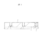
次に、図8に示すように、プラグ22の上部にバリア層23を形成する。バリア層23を形成するには、窒化シリコン膜18の上部にスパッタリング法でWN膜を堆積した後、続いてスルーホール19の外部のWN膜を化学機械研磨法(またはドライエッチング)で除去する。バリア層23は、後述する製造工程の途中で行われる熱処理によって、下部電極30Aを構成するRu(ルテニウム)とプラグ22を構成する多結晶シリコンとが不所望のシリサイド反応を引き起こすのを防ぐために形成する。なお、このバリア層23をW膜もしくはTaN(窒化タンタル)膜により形成してもよい。
【0033】
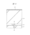
この後、プラグ22上に、Ru膜30からなる下部電極30A、酸化タンタル膜32からなるキャパシタ絶縁膜およびW膜/Ru膜からなる上部電極33によって構成される情報蓄積用容量素子(キャパシタ)Cを形成する。
【0034】
この情報蓄積用容量素子Cの形成工程を、図9〜図17を参照しながら詳細に説明する。これらの図は、プラグ22上の情報蓄積用容量素子Cの形成予定領域を模式的に表した図である。
【0035】
図9に示すように、バリア層23および窒化シリコン膜18上に、酸化シリコン膜24を堆積する。情報蓄積用容量素子Cの下部電極は、この酸化シリコン膜24に形成する孔(凹部)の内部に形成される。下部電極の表面積を大きくして蓄積電荷量を増やすためには、酸化シリコン膜24を厚く(0.8μm程度)堆積する必要がある。酸化シリコン膜24は、例えば酸素とテトラエトキシシラン(TEOS)とをソースガスに用いたプラズマCVD法で堆積し、その後、必要に応じてその表面を化学機械研磨法で平坦化する。
【0036】
次に、酸化シリコン膜24の上部にスパッタリング法で膜厚200nm程度のW膜を堆積し、続いてW膜の上部に反射防止膜を塗布することにより、ハードマスク26を形成する。このハードマスク26(W膜)は、酸化シリコン膜24に対するエッチング選択比がフォトレジスト膜に比べて大きいので、厚い膜厚の酸化シリコン膜24をエッチングする際のマスクとして使用される。
【0037】
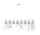
次に、図10に示すように、ハードマスク26上に、フォトレジスト膜(図示せず)を形成し、このフォトレジスト膜をマスクに、ハードマスク26をドライエッチングする。続いて、ハードマスク26をマスクに酸化シリコン膜24をドライエッチングすることにより、深い孔(凹部)27を形成する。深い孔(凹部)27の底面には、スルーホール19内のバリア層23の表面が露出する。
【0038】
次に、酸化シリコン膜24の上部に残ったハードマスク26を過酸化水素水を含有する溶液により除去した後、図11に示すように、酸化シリコン膜24の上部および孔27の内部に、スパッタ法によりWN膜29(膜厚15nm程度)を堆積する。このWN膜29は、下地である酸化シリコン膜24や、後述するRu膜30との接着性に優れているため、接着層として用いられる。また、このWN膜29は、後述するRu膜30の形成時に結晶成長の種となり、Ru膜30の成膜性を良くする。
【0039】
次いで、図12に示すように、WN膜29の上部に、CVD法によりRu膜30(膜厚30nm程度)を堆積するのであるが、このCVD法によるRu膜の堆積前に、スパッタ法により膜厚15nm程度のRu膜(図示せず)を形成する。これは、スパッタ法により形成された膜が種となり、CVD法によるRu膜30を効率良く成長させるためである。
【0040】
このRu膜30は、Ruのアセチルアセトン誘導体化合物であるRu(HFAC)3、H2O(水蒸気)およびH2(水素)を原料として形成する。なお、HFACは、(CF3COCHCOCF3)-を意味する。このCF3基の代わりに、C(CH3)3基が結合した化合物を用いても良い。また、Ru(HFAC)(1,5−cyclooctadiene)を用いてもよい。
【0041】
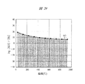
このRu(HFAC)3の有機化合物溶液を気化し、H2OおよびH2と反応させることにより成膜する。なお、有機化合物溶液としては、テトラヒドロフラン溶液等が挙げられる。ここで、H2OおよびH2の分圧比を図13に示すグラフ(a)より下の領域に位置するよう制御しつつ反応を起こさせる。
【0042】
まず、このRu膜の成膜の反応機構について説明する。この反応機構としては、図14に示す機構が考えられる。図14に示すように、Ru(HFAC)3は、まず、H2Oと反応し(H2Oにより分解され)、水酸化物Ru(OH)3となる(図14(a))。次いで、この水酸化物Ru(OH)3が水素により還元され、Ruが生成する(図14(b))。この反応機構から明らかなように、H2Oは消費されず、触媒的な働きをする。なお、反応が行われる反応室は、排気されているため、実質的な原料であるRu(HFAC)3やH2と同様に、H2Oも適宜供給する必要がある。
【0043】
このように、本実施の形態によれば、Ru(HFAC)3、H2OおよびH2を用いて、加水分解利用し、Ru膜を形成したので、膜質の良好なRu膜を形成することができる。
【0044】
例えば、エトキシシクロペンタジエニルルテニウム(Ru(C2H5OC5H4)2)のテトラヒドロフラン溶液等のRuの有機化合物溶液を気化し、O2と反応させることによりRu膜を成膜することも可能である。しかしながら、この場合は、Ruが酸化しないよう不完全燃焼を起こさせることによりRuを生成する反応である。その結果、炭素や水素もしくはこれらの酸素化合物の他、反応の際に生じる有機化合物やその酸化物がRu膜中に取りこまれ、Ru膜の膜質を劣化させる原因となる。さらに、この後に行われる熱処理、例えば、Ru膜のデンシファイ(緻密化)のための熱処理等により、Ru膜中に取り込まれた炭素や水素もしくはこれらの酸素化合物等が気化し、Ru膜の膜質を劣化させる。また、Ru膜中の酸素や酸素化合物が、接着層となるWN膜29やバリア層23を酸化し、プラグ22と下部電極(Ru膜30)との導通不良を引き起こす。特に、前述のように、プラグ22の径が小さい場合には導通不良が起こり易い。
【0045】
これに対し、本実施の形態によれば、Ru(HFAC)3の加水分解を利用してRu膜を生成したので、Ru膜中に取り込まれる副生成物、例えば、炭素や水素もしくはこれらの化合物を低減することができる。即ち、結晶性のよいRu膜を形成することができるため、この後に行われる熱処理、例えば、Ru膜のデンシファイ(緻密化)のための熱処理等により、Ru膜中に取り込まれた炭素や水素もしくはこれらの酸素化合物等が気化しても、気化量が少なくRu膜の膜質を維持することができる。また、後述する下部電極(Ru膜30)上に形成される容量絶縁膜の熱処理時においても、Ru膜中の炭素等の気化による膜収縮を小さくでき、容量絶縁膜の破損を防止することができる。その結果、情報蓄積用容量素子Cの特性を向上させることができる。また、Ru膜中の酸素や酸素化合物量を低減することができ、プラグ22と下部電極(Ru膜30)との導通不良を防止することができる。
【0046】
また、H2OおよびH2の分圧比を図13に示すグラフ(a)より下の領域に位置するよう制御するのは、Ru膜の成膜時に、Ruが酸化するのを抑えるためである。即ち、Ru膜の成膜時には、生成したRuとH2Oとの反応によりRuO2(酸化ルテニウム)が生じるという副反応が起こり得る。以下、この反応(Ruの酸化)を抑えることができる理由について以下に説明する。
【0047】
この図13のグラフ(a)は、系1(RuO2+H2)と系2(Ru+H2O)との平衡状態における平衡定数kの対数を、反応温度について表したものである。このlogk=log[[H2O]eq/[H2]eq]([H2O]eq:平衡状態におけるH2Oの分圧、[H2]eq:平衡状態におけるH2の分圧)により表される。また、この平衡定数kは、系1と系2とのギプスの自由エネルギーの差(ΔG)等により、ΔG=−RTlnkより求めることができる。
【0048】
従って、このグラフ(a)より上の領域に位置する条件下においては、Ruが酸化される方向に平衡が移動してしまう。しかしながら、H2OおよびH2の分圧比を図13に示すグラフ(a)より下の領域に位置するよう制御しつつ、Ru膜を成膜すると、Ruの酸化を抑えることができる。
【0049】
但し、Ru膜の成膜には、原料であるRu(HFAC)3溶液を気化する必要があり、また、あまり高温で処理すると原料の分解が起こりうるため、反応温度は、100〜200℃(原料溶液の沸点以上)から500℃程度が好ましいと思われる。
【0050】
このように、本実施の形態によれば、Ru(HFAC)3、H2OおよびH2を用い、さらに、H2OおよびH2の分圧比を図13に示すグラフ(a)より下の領域に位置するよう制御しつつ反応を起こさせたので、Ru膜の酸化を防ぎつつ、酸素や炭素もしくはこれらの化合物の含有量が少ない良好なRu膜を形成することができる。
【0051】
次いで、700℃、1分間の熱処理を行いRu膜30をデンシファイ(緻密化)する。なお、前述のようにRu膜の結晶性がよいので、この熱処理により気化するRu膜中の炭素等が少なく、Ru膜の膜質を維持することができる。
【0052】
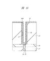
次いで、図15に示すように、Ru膜30上にフォトレジスト膜(図示せず)を塗布し、全面露光を行った後、現像することによって、孔27内にフォトレジスト膜(図示せず)を残存させる。このフォトレジスト膜は、次の工程で酸化シリコン膜24の上部の不要なRu膜30をドライエッチングで除去する際に、孔27の内部(側壁および底面)のRu膜30が除去されるのを防ぐ保護膜として使用される。次いで、このフォトレジスト膜をマスクに、ドライエッチングをすことにより、酸化シリコン膜24上のRu膜30を除去することにより下部電極30Aを形成する。次いで、孔27内のフォトレジスト膜を除去する。
【0053】
次に、下部電極30Aが形成された孔27の内部および酸化シリコン膜24上にキャパシタ絶縁膜となる10nm程度の酸化タンタル膜32を堆積する。酸化タンタル膜32はペンタエトキシタンタル(Ta(OC2H5)5)と酸素を原料としたCVD法で堆積する。その後、Ar(アルゴン)雰囲気中で650℃の熱処理を施し、酸化タンタルを結晶化させる。なお、前述のようにRu膜の結晶性がよいので、この熱処理時のRu膜の膜収縮を小さくでき、酸化タンタル膜32の破損を防止することができる。
【0054】
次に、図16に示すように、酸化タンタル膜32の上部に上部電極33を形成する。上部電極33は、例えば酸化タンタル膜32の上部にCVD法でRu膜33a(膜厚70nm程度)およびW膜33b(膜厚100nm程度)を堆積することによって形成する。Ru膜33aは、Ru膜30と同様に形成してもよい。W膜33bは、上部電極33と上層配線とのコンタクト抵抗を低減するために使用される。なお、Ru膜33aとW膜33bとの間に、キャパシタ絶縁膜(酸化タンタル膜32)からW膜へのガス(酸素や水素)の拡散による抵抗増大を防ぐためにTiN膜を形成してもよい。
【0055】
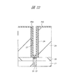
ここまでの工程により、Ru膜30からなる下部電極30A、酸化タンタル膜32からなるキャパシタ絶縁膜およびW膜33b/Ru膜33aからなる上部電極33によって構成される情報蓄積用容量素子Cが完成し、メモリセル選択用MISFETQsとこれに直列に接続された情報蓄積用容量素子Cとで構成されるDRAMのメモリセルが略完成する。図17は、情報蓄積用容量素子C形成後の半導体集積回路装置の平面図である。図7は、例えば、図17中のA−A部の断面図と対応する。
【0056】
その後、情報蓄積用容量素子Cの上部に酸化シリコン膜等からなる層間絶縁膜34が形成され、さらに、この層間絶縁膜上に2層程度のAl配線が形成され、最上層のAl配線の上部にパッシベーション膜が形成されるが、これらの図示は省略する。
【0057】
以上詳述したように、本実施形態によれば、Ru(HFAC)3の加水分解を利用してRu膜を生成したので、Ru膜中に取り込まれる副生成物を低減することができ、Ru膜の膜質を向上させることができる。
【0058】
また、本実施の形態においては、Ru膜の成膜時に用いられるH2OおよびH2の分圧比を図13に示すグラフ(a)より下の領域に位置するよう制御したので、Ru膜の成膜時に、Ruの酸化を抑えることができる。
【0059】
その結果、情報蓄積用容量素子Cの特性を向上させ、また、メモリセルの特性を向上させることができる。また、微細化されたメモリセル構造においても所望の容量を確保することができる。
【0060】
(実施の形態2)
実施の形態1においては、Ru(HFAC)3、H2OおよびH2を原料とし、H2OおよびH2の分圧比を図13に示すグラフ(a)より下の領域に位置するよう制御し、Ru膜30を形成したが、Ru膜の形成に際し、H2OおよびH2の分圧比を以下に説明する条件下で形成してもよい。
【0061】
以下、本実施形態のDRAMの製造方法を説明する。なお、接着層としての働きを有するWN膜29の形成工程までは、図1〜図11までを参照しながら説明した実施の形態1の場合と同様と同様であるためその説明を省略する。
【0062】
このWN膜29の上部に、図18に示すように、スパッタ法により膜厚15nm程度のRu膜(図示せず)を形成し、次いで、CVD法により膜厚30nm程度のRu膜230を堆積する。
【0063】
ここで、このRu膜230を、実施の形態1と同様に、Ru(HFAC)3、H2OおよびH2を原料として形成するのであるが、この際、H2OおよびH2の分圧比を図19に示すグラフ(b)より下の領域に位置するよう制御しつつ反応を起こさせる。
【0064】
図19のグラフ(a)は、系1(RuO2+H2)と系2(Ru+H2O)との平衡状態における平衡定数kの対数を、反応温度について表したものであり、グラフ(b)は、系1(WO2+H2)と系2(W+H2O)との平衡状態における平衡定数kの対数を、反応温度について表したものである。実施の形態1で説明したように、このlogk=log[[H2O]eq/[H2]eq]([H2O]eq:平衡状態におけるH2Oの分圧、[H2]eq :平衡状態におけるH2の分圧)により表され、この平衡定数kは、系1と系2とのギプスの自由エネルギーの差(ΔG)等により求めることができる。
【0065】
従って、このグラフ(b)より上の領域に位置する条件下においては、Wが酸化される方向に平衡が移動してしまう。しかしながら、H2OおよびH2の分圧比を図19に示すグラフ(b)より下の領域に位置するよう制御しつつ、Ru膜を成膜すると、Ruの酸化を抑えつつ、Wの酸化をも抑えることができる。
【0066】
その結果、実施の形態1で説明した効果に加え、接着層の役割を果たすWN膜29やバリア層23中のWの酸化を抑えることができる。その結果、Ru膜230(下部電極)とプラグ22との間の導通不良を防止することができる。なお、WN膜29やバリア層23をW膜で形成した場合も同様に、Wの酸化を抑えることもできる。また、WN膜29やバリア層23をTaN膜で形成した場合は、Ru膜の形成時に、H2OおよびH2の分圧比を図20に示すグラフ(c)より下の領域に位置するよう制御しつつ反応を起こさせると、TaN膜中のTaの酸化を抑えることができる。図20のグラフ(c)は、系1(Ta2O5+H2)と系2(Ta+H2O)との平衡状態における平衡定数kの対数を、反応温度について表したものである。
【0067】
次いで、700℃、1分間の熱処理を行いRu膜230をデンシファイ(緻密化)する。
【0068】
以降の工程は、図15および図16を参照しながら説明した実施の形態1の場合と同様であるためその説明を省略する。
【0069】
以上詳述したように、本実施形態によれば、Ru膜230をRu(HFAC)3、H2OおよびH2を原料とし、このうちのH2OおよびH2の分圧比を図19に示すグラフ(b)より下の領域に位置するよう制御しつつ形成したので、Ru膜の下層に位置するWもしくはWの化合物より成る膜の酸化を抑えることができ、Ru膜230(下部電極)とプラグ22との間の導通不良を防止することができる。その結果、情報蓄積用容量素子Cの特性を向上させ、また、メモリセルの特性を向上させることができる。
【0070】
なお、実施の形態1および2では、Ru膜を例に説明したが、Ir(イリジウム)膜、Pd(パラジウム)もしくはPt(白金)等もヘキサフロロアセチルアセトンと錯体化合物(アセチルアセトネイト誘導体)をつくり得るので、これらの錯体化合物、H2OおよびH2を原料とし、実施の形態1および2のように、H2OおよびH2の分圧比を制御しつつこれらの金属膜を形成すれば、同様の効果を得ることができる(図21参照)。図21のグラフ(d)(e)は、それぞれ系1(IrO2+H2)と系2(Ir+H2O)との平衡状態における平衡定数kの対数、系1(PdO+H2)と系2(Pd+H2O)との平衡状態における平衡定数kの対数を、反応温度について表したものである。特に、RuやIrは、前述の錯体化合物を得やすく、下部電極として用いて好適である。
【0071】
(実施の形態3)
実施の形態1および2においては、Ru膜成膜時のH2OおよびH2の分圧比を制御したが、キャパシタ絶縁膜となる酸化タンタル膜(Ta2O5)を以下に説明するようにH2OおよびH2の分圧比を制御して形成してもよい。
【0072】
以下、本実施形態のDRAMの製造方法を説明する。なお、下部電極30A形成工程までは、図1〜図15までを参照しながら説明した実施の形態1の場合と同様と同様であるためその説明を省略する。なお、下部電極30Aを構成するRu膜30を実施の形態2で説明した方法で形成してもよい。
【0073】
この下部電極30Aが形成された孔27の内部および酸化シリコン膜24上に、図22に示すように、キャパシタ絶縁膜となる10nm程度の酸化タンタル膜332を堆積する。酸化タンタル膜332はペンタエトキシタンタル(Ta(OC2H5)5)とH2Oを原料としたCVD法で堆積する。
【0074】
このように、本実施の形態によれば、ペンタエトキシタンタル(Ta(OC2H5)5)とH2Oを用いて酸化タンタル膜332を形成したので、膜質の良好な酸化タンタル膜332を形成することができる。
【0075】
即ち、実施の形態1で説明したように、ペンタエトキシタンタル(Ta(OC2H5)5)と酸素を原料としたCVD法で、酸化タンタル膜332を堆積してもよいが、この場合は、炭素もしくはその化合物等が酸化タンタル膜332中に取りこまれ、酸化タンタル膜の膜質を劣化させる原因となる。また、原料として酸素を用いるため、酸化タンタル膜332の下層である下部電極30A(Ru膜)、接着層の役割を果たすWN膜29やバリア層23を酸化してしまう恐れがある。これらの膜が酸化されると、Ru膜30(下部電極)とプラグ22との間の導通不良を引き起こす。特に、プラグの径が小さい場合には導通不良が起こり易い。
【0076】
これに対し、本実施の形態によれば、ペンタエトキシタンタル(Ta(OC2H5)5)の加水分解を利用して酸化タンタル膜332を生成したので、酸化タンタル膜332中に取り込まれる副生成物、例えば、炭素やこの化合物を低減することができ、膜質のよい酸化タンタル膜332を形成することができる。また、原料として酸素を用いないので、酸化タンタル膜332の下層膜の酸化を防止することができ、プラグ22と下部電極(Ru膜)30Aとの導通不良を防止することができる。
【0077】
また、ペンタエトキシタンタル(Ta(OC2H5)5)とH2Oの他、H2を用いて以下に説明する条件で酸化タンタル膜332を形成してもよい。
【0078】
即ち、H2OおよびH2の分圧比を図23に示すグラフ(a)とグラフ(c)で囲まれた領域に位置するよう制御しつつ反応を起こさせる。
【0079】
図23のグラフ(c)は、系1(Ta2O5+H2)と系2(Ta+H2O)との平衡状態における平衡定数kの対数を、反応温度について表したものである。実施の形態1で説明したように、このlogk=log[[H2O]eq/[H2]eq]([H2O]eq:平衡状態におけるH2Oの分圧、[H2]eq:平衡状態におけるH2の分圧)により表され、この平衡定数kは、系1と系2とのギプスの自由エネルギーの差(ΔG)等により求めることができる。
【0080】
従って、このグラフ(c)より下の領域に位置する条件下においては、Ta2O5が還元される方向に平衡が移動してしまうため、酸化タンタル膜332を成膜するには、H2OおよびH2の分圧比を図23に示すグラフ(c)より上の領域に位置するよう制御する必要がある。ここで、実施の形態1で説明したように、H2OおよびH2の分圧比を図23に示すグラフ(a)より下の領域に位置するよう制御すれば、Ruの酸化を抑えることができる。但し、酸化タンタル膜の成膜には、原料溶液を気化する必要があり、また、あまり高温で処理すると原料の分解が起こりうるため、反応温度は、100〜200℃(原料溶液の沸点以上)から500℃程度が好ましいと思われる。
【0081】
このように、本実施の形態によれば、ペンタエトキシタンタル(Ta(OC2H5)5)、H2OおよびH2を用い、さらに、H2OおよびH2の分圧比を図23に示すグラフ(a)およびグラフ(c)で囲まれた領域に位置するよう制御しつつ反応を起こさせたので、Ru膜の酸化を防ぎつつ、酸化タンタル膜332を成膜することができる。
【0082】
また、H2OおよびH2の分圧比を図24に示すグラフ(b)とグラフ(c)で囲まれた領域に位置するよう制御しつつ反応を起こさせると、実施の形態2で説明したようにRu膜やWN膜の酸化を防ぎつつ、酸化タンタル膜332を成膜することができる。
【0083】
次いで、Ar(アルゴン)雰囲気中で650℃の熱処理を施し、酸化タンタル膜332を結晶化させる。
【0084】
次いで、実施の形態1の場合と同様に、酸化タンタル膜332の上部に上部電極33を形成する(図16参照)。
【0085】
以上詳述したように、本実施形態によれば、ペンタエトキシタンタル(Ta(OC2H5)5)、H2OおよびH2を用い、さらに、H2OおよびH2の分圧比を制御しつつ反応を起こさせたので、酸化タンタル膜332の下層の膜(Ru膜やWN膜)の酸化を防ぎつつ、酸化タンタル膜332を成膜することができる。
【0086】
従って、Ru膜30(下部電極)とプラグ22との間の導通不良を防止することができる。その結果、情報蓄積用容量素子Cの特性を向上させ、また、メモリセルの特性を向上させることができる。
【0087】
なお、本実施の形態においては、キャパシタ絶縁膜として酸化タンタル膜を用いたが、Al2O3やBST(BaXSr1-XTiO3)を用いてもよい。
【0088】
Al(CH3)2H(ジメチルアルミニウムハイドライド)、H2OおよびH2を原料とし、本実施の形態のように、H2OおよびH2の分圧比を制御しつつAl2O3膜を形成すれば、同様の効果を得ることができる。
【0089】
また、BST膜は、Ba(C(CH3)3-CO-CH-CO-C(CH3)3)2 bis(dipivaloylmetanate)barium、Sr(C(CH3)3-CO-CH-CO-C(CH3)3)2 bis(dipivaloylmetanate)strontium、もしくはTiO(C(CH3)3-CO-CH-CO-C(CH3)3)2 titanylbis(dipivaloylmetanate)と、H2OおよびH2を原料として形成することができ、この場合も、本実施の形態のように、H2OおよびH2の分圧比を制御しつつBST膜を形成すれば、同様の効果を得ることができる。
【0090】
なお、実施の形態1〜3では、DRAMメモリセルを例に説明したが、DRAMに限られず、本発明は、MIM(Metal Insulator Metal)キャパシタを有する半導体集積回路に広く適用することができる。
【0091】
(実施の形態4)
実施の形態1〜3では、DRAMの情報蓄積用容量素子部に本発明を適用したが、本発明を配線部に適用してもよい。次に、本発明の実施の形態である半導体集積回路装置の製造方法について説明する。図25〜図28および図32〜図35は、本発明の実施の形態である半導体集積回路装置の製造方法を示した基板の要部断面図である。
【0092】
まず、図25に示すように、通常のMISFET形成プロセスにより、nチャネル型MISFETQnおよびpチャネル型MISFETQpを形成する。
【0093】
通常のMISFET形成プロセスには、例えば、次のようなものがある。
【0094】
まず、p型の単結晶シリコンからなる半導体基板401をエッチングすることにより素子分離溝402を形成し、基板401を熱酸化することによって、溝の内壁に薄い酸化シリコン膜を形成する。次に、溝の内部を含む基板401上にCVD法で酸化シリコン膜407を堆積し、化学的機械研磨法で溝の上部の酸化シリコン膜407を研磨し、その表面を平坦化する。
【0095】
次に、基板401にp型不純物およびn型不純物をイオン打ち込みした後、熱処理により不純物を拡散させることによって、p型ウエル403およびn型ウエル404を形成した後、熱酸化によりp型ウエル403およびn型ウエル404のそれぞれの表面に膜厚6nm程度の清浄なゲート酸化膜408を形成する。
【0096】
次に、ゲート酸化膜408の上部にリンをドープした低抵抗多結晶シリコン膜409aをCVD法で堆積し、続いてその上部にスパッタリング法で薄いWN膜(図示せず)とW膜409bとを堆積し、さらにその上部にCVD法で窒化シリコン膜410を堆積する。
【0097】
次に、窒化シリコン膜410をドライエッチングすることにより、ゲート電極を形成する領域に窒化シリコン膜410を残し、窒化シリコン膜410をマスクにしてW膜409b、WN膜(図示せず)および多結晶シリコン膜409aをドライエッチングすることにより、多結晶シリコン膜409a、WN膜およびW膜409bからなるゲート電極409を形成する。
【0098】
次に、ゲート電極409の両側のp型ウエル403にn型不純物をイオン打ち込みすることによってn-型半導体領域411を形成し、n型ウエル404にp型不純物をイオン打ち込みすることによってp-型半導体領域412を形成する。
【0099】
次に、基板401上にCVD法で窒化シリコン膜を堆積した後、異方的にエッチングすることによって、ゲート電極409の側壁にサイドウォールスペーサ413を形成する。
【0100】
次に、p型ウエル403にn型不純物をイオン打ち込みすることによってn+型半導体領域414(ソース、ドレイン)を形成し、n型ウエル404にp型不純物をイオン打ち込みすることによってp+型半導体領域415(ソース、ドレイン)を形成する。
【0101】
ここまでの工程で、LDD(Lightly Doped Drain)構造のソース、ドレインを備えたnチャネル型MISFETQnおよびpチャネル型MISFETQpが形成される。
【0102】
この後、MISFETQnおよびQp上に酸化シリコン膜等の層間絶縁膜と銅膜等の導電性膜を交互に堆積し、複数の配線を形成するのであるが、以下層間絶縁膜と配線の形成について図26〜図35を参照しながら詳細に説明する。
【0103】
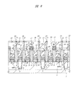
まず、図26に示すようにMISFETQnおよびQp上にCVD法で膜厚700nm〜800nm程度の酸化シリコン膜を堆積した後、酸化シリコン膜を化学機械研磨法で研磨してその表面を平坦化することによって層間絶縁膜TH1を形成する。
【0104】
次に、層間絶縁膜TH1上にフォトレジスト膜を形成し(図示せず)、このフォトレジスト膜をマスクに層間絶縁膜TH1をエッチングすることにより半導体基板401主面のn+型半導体領域414およびp+型半導体領域415上にコンタクトホールC1を形成する。
【0105】
次いで、図27に示すようにコンタクトホールC1内を含む層間絶縁膜TH1上に、CVD法によりタングステン膜を堆積し、このタングステン膜を層間絶縁膜TH1が露出するまで化学機械研磨法により研磨することによってコンタクトホールC1内にプラグP1を形成する。なお、タングステン膜の堆積前に、薄いTiN膜を堆積し、プラグP1を、TiN膜等からなるバリア膜とタングステン膜との積層構造としてもよい。
【0106】
次いで、層間絶縁膜TH1およびプラグP1上に、窒化シリコン膜H1aおよび酸化シリコン膜H1bをCVD法により順次堆積し、これらの膜から成る配線溝用絶縁膜H1を形成する。第1層配線形成予定領域の配線溝用絶縁膜H1をエッチングすることにより配線溝HM1を形成する。なお、窒化シリコン膜H1aは、前記エッチングの際のエッチングストッパーとして利用される。
【0107】
次に、図28に示すように、配線溝HM1内を含む配線溝用絶縁膜H1上に窒化タングステンからなるバリア層M1aをスパッタ法により堆積し、次いで、バリア層M1a上に、銅膜M1bをCVD法により形成する。
【0108】
この銅膜M1bは、Cu(銅)の化合物であるCu(HFAC)2、H2OおよびH2を原料として形成する。なお、HFACは、(CF3COCHCOCF3)-を意味する。
【0109】
このCu(HFAC)2の有機化合物溶液を気化し、H2OおよびH2と反応させることにより成膜する。なお、有機化合物溶液としては、テトラヒドロフラン溶液等が挙げられる。ここで、H2OおよびH2の分圧比を図29に示すグラフ(a’)より下の領域に位置するよう制御しつつ反応を起こさせる。
【0110】
このように制御するのは、Cu膜の成膜時に、Cuの酸化を抑えるためである。このCuの酸化を抑えることができる理由についてもRuの場合と同様に説明することができる。
【0111】
つまり、この図29は、系1(CuO+H2)と系2(Cu+H2O)との平衡状態における平衡定数kの対数を、反応温度について表したものである。このlogk=log[[H2O]eq/[H2]eq]([H2O]eq:平衡状態におけるH2Oの分圧、[H2]eq:平衡状態におけるH2の分圧)により表される。また、この平衡定数kは、系1と系2とのギプスの自由エネルギーの差(ΔG)等により、ΔG=−RTlnkより求めることができる。
【0112】
従って、このグラフ(a’)より上の領域に位置する条件下においては、Cuが酸化される方向に平衡が移動してしまう。しかしながら、H2OおよびH2の分圧比を図29に示すグラフ(a’)より下の領域に位置するよう制御しつつ、Cu膜を成膜すると、Cuの酸化を抑えることができる。
【0113】
但し、Cu膜の成膜には、原料であるCu(HFAC)2溶液を気化する必要があり、また、あまり高温で処理すると原料の分解が起こり得るため、反応温度は、100〜200℃(原料溶液の沸点以上)から500℃程度が好ましいと思われる。
【0114】
このように、本実施の形態によれば、Cu(HFAC)2、H2OおよびH2を用い、さらに、H2OおよびH2の分圧比を図29に示すグラフ(a’)より下の領域に位置するよう制御しつつ反応を起こさせたので、Cu膜の酸化を防ぎつつ、酸素や炭素もしくはこれらの化合物の含有量が少ない良好なCu膜を形成することができる。
【0115】
また、このCu膜M1bを、H2OおよびH2の分圧比を図30に示すグラフ(b)より下の領域に位置するよう制御しつつ反応を起こさせれば、成膜中のCuや、窒化タングステンからなるバリア層M1a中のWの酸化を抑えることができる。
【0116】
図30のグラフ(b)は、系1(WO2+H2)と系2(W+H2O)との平衡状態における平衡定数kの対数を、反応温度について表したものである。前述したように、このlogk=log[[H2O]eq/[H2]eq]([H2O]eq:平衡状態におけるH2Oの分圧、[H2]eq:平衡状態におけるH2の分圧)により表され、この平衡定数kは、系1と系2とのギプスの自由エネルギーの差(ΔG)等により求めることができる。
【0117】
従って、このグラフ(b)より上の領域に位置する条件下においては、Wが酸化される方向に平衡が移動してしまう。しかしながら、H2OおよびH2の分圧比を図30に示すグラフ(b)より下の領域に位置するよう制御しつつ、Cu膜を成膜すると、Cuの酸化を抑えつつ、Wの酸化をも抑えることができる。
【0118】
従って、成膜中のCuや、窒化タングステンからなるバリア層M1a中のWの酸化を抑えることができる。その結果、Cu膜M1bとプラグP1との間の導通不良を防止することができる。また、バリア層M1a中のWの酸化を抑えることによりバリア性の低下を防ぐことができる。その結果、Cuの絶縁膜中への拡散による配線間ショートを防止することができる。
【0119】
この銅膜M1bを、Cuの陽イオンとヘキサフロロアセチルアセトン(CF3COCHCOCF3)-およびトリメチルビニルシラン(CH2CHSi(CH3)3)の化合物であるCu(HFAC)(TMVS)、H2OおよびH2を原料として形成してもよい。なお、HFACは、(CF3COCHCOCF3)-を、TMVSは、(CH2=CHSi(CH3)3)を意味する。
【0120】
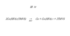
このCu(HFAC)(TMVS)の有機化合物溶液を気化し、H2OおよびH2と反応させることにより成膜する。なお、有機化合物溶液としては、テトラヒドロフラン溶液等が挙げられる。このCu膜の成膜の反応を、図31に示す。この反応においてもH2Oが触媒的な働きをし、H2Oを添加することによって反応速度が大きくなる。
【0121】
この反応の際も、前述したように、H2OおよびH2の分圧比を図29に示すグラフ(a’)より下の領域に位置するよう制御すれば、Cuの酸化を抑えることができる。また、H2OおよびH2の分圧比を図30に示すグラフ(b)より下の領域に位置するよう制御すれば、Cuの酸化を抑えつつ、Wの酸化をも抑えることができる。その結果、Cu膜M1bとプラグP1との間の導通不良や配線間ショートを防止することができる。
【0122】
次に、図32に示すように、配線溝HM1外部の銅膜M1bおよびバリア層M1aを化学機械研磨法により除去することにより銅膜M1bおよびバリア層M1aから成る第1層配線M1を形成する。
【0123】
次に、図33に示すように第1層配線M1上に、CVD法によりシリコン窒化膜を堆積することにより銅拡散防止用絶縁膜D1を形成した後、層間絶縁膜TH2を形成する。層間絶縁膜TH2は、前記層間絶縁膜TH1と同様に形成する。
【0124】
次いで、層間絶縁膜TH2上に第1層配線M1のコンタクト領域上が開孔したレジスト膜(図示せず)を形成し、これをマスクに第1層配線M1の表面が露出するまで、層間絶縁膜TH2および銅拡散防止用絶縁膜D1を異方的にエッチングする。
【0125】
次いで、図34に示すように、コンタクトホールC2内を含む層間絶縁膜TH2上に、TiN等の高融点金属の窒化物を30〜70nm堆積することによりバリア層P2aを形成する。次いで、バリア層P2a上に、CVD法により200〜500nm程度のタングステン膜P2bを堆積する。なお、タングステン膜P2bは、コンタクトホールC2内を完全に埋め込むよう形成する。
【0126】
続いて、コンタクトホールC2外のタングステン膜P2bおよびバリア層P2aを化学機械研磨により除去することにより、タングステン膜P2bおよびバリア層P2aから成るプラグP2を形成する。
【0127】
次いで、図35に示すように、プラグP2上に第2層配線M2を、第1層配線M1と同様に形成する。即ち、層間絶縁膜TH2およびプラグP2上に、窒化シリコン膜H2aおよび酸化シリコン膜H2bを順次堆積し、これらの膜から成る配線溝用絶縁膜H2をエッチングすることにより配線溝HM2を形成する。次に、配線溝HM2内を含む配線溝用絶縁膜H2上に窒化チタンからなるバリア層M2aを堆積し、次いで、バリア層M2a上に、銅膜M2bをCVD法により前述の条件で形成する。次に、配線溝HM2外部の銅膜M2bおよびバリア層M2aを化学機械研磨により除去することにより銅膜M2bおよびバリア層M2aから成る第2層配線M2を形成する。
【0128】
次いで、第2層配線M2上に、銅拡散防止絶縁膜D2および層間絶縁膜TH3を形成する。これらの膜は、前記銅拡散防止絶縁膜D1および層間絶縁膜TH1と同様に形成する。その後、銅拡散防止絶縁膜D2および層間絶縁膜TH3中にコンタクトホールC3を形成し、コンタクトホールC3内にプラグP3を形成する。このプラグP3は、プラグP2と同様に形成する。次いで、層間絶縁膜TH3およびプラグP3上に、配線溝用絶縁膜H1および配線溝HM1と同様に、配線溝用絶縁膜H3および配線溝HM3を形成し、第1層配線M1と同様に第3層配線M3を形成する。
【0129】
この配線上の銅拡散防止絶縁膜(D3、D4、D5)および層間絶縁膜(TH4、TH5)の形成、これら膜中のコンタクトホール内に形成されたプラグ(P4、P5)の形成およびプラグ上の配線(M4、M5)の形成を繰り返すことにより多層配線構造の半導体集積回路装置を形成することができる。
【0130】
続いて、第5層配線M5上に窒化シリコン膜および酸化シリコン膜等から成るパッシベーション膜420を形成し、このパッシベーション膜420の一部をエッチングにより除去することにより第5層配線M5上のボンディングパッド部を露出させる(図示せず)。次いで、露出した第5層配線M5上に金等からなるバンプ下地電極を形成し、バンプ下地電極上に金もしくは半田等からなるバンプ電極を形成する(図示せず)。
【0131】
この後、パッケージ基板等に実装され半導体集積回路装置が完成するが、それらの説明は省略する。
【0132】
なお、本実施の形態では、5層の配線を形成したが、5層以下もしくは5層以上の配線をしてもよい。また、本実施の形態においては、半導体素子としてMISFETQnおよびQpを形成したが、これらMISFETに限られず、バイポーラトランジスタ等のその他の素子を形成することもできる。また、CVD法により形成された金属配線を有する半導体集積回路装置に広く適用することができる。
【0133】
(実施の形態5)
実施の形態1では、Ru膜の成膜時にH2OおよびH2の分圧比を制御したが、この膜をH2の代わりにアルコールを用いて成膜してもよい。
【0134】
以下、本実施形態のDRAMの製造方法を説明するが、Ru膜の成膜時に、還元剤としてH2の代わりにアルコールを用いる他は、実施の形態1の場合と同様であるため、Ru膜の成膜工程についてのみ以下に説明する。
【0135】
例えば、実施の形態1で説明した図11のWN膜29の上部に、スパッタ法により膜厚15nm程度のRu膜(図示せず)を形成し、次いで、CVD法により膜厚30nm程度のRu膜30を堆積する(図12参照)。
【0136】
ここで、このRu膜30を、Ru(HFAC)3、H2Oおよびアルコールを原料として形成する。このアルコールとしては、2級以下のアルコール、例えば、メタノール、エタノールもしくはイソプロピルアルコール等を用いることができる。
【0137】
まず、このRu膜の成膜の反応機構について説明する。Ru(HFAC)3は、まず、H2Oと反応し(H2Oにより分解され)、水酸化物Ru(OH)3となる。次いで、この水酸化物Ru(OH)3がアルコール(R−OH)により還元され、Ruが生成する。この際、アルコールは、酸化されアルデヒドもしくはケトンとなる。
【0138】
図36に、イソプロピルアルコールを用いた場合の反応機構を示す。また、Ru(HFAC)3の代わりにRu(DPM)3を用いてもよい(図37)。ここで、DPMとは、((CH3)3CCOCHCOC(CH3)3)-を意味する。このような反応は、常温、大気圧下において、68kJ程度の発熱反応であり、容易に進行する。
【0139】
このように、本実施の形態によれば、Ru(HFAC)3、H2Oおよびアルコールを用いて、加水分解利用し、Ru膜を形成したので、実施の形態1で説明したように、膜質の良好なRu膜を形成することができる。
【0140】
さらに、アルコールは、H2に比べ扱い易いため、容易にRu膜を形成することができる。
【0141】
なお、本実施の形態においては、Ru膜を例に説明したが、Ir化合物、H2Oおよびアルコールを原料とし、Ir膜を形成すれば、同様の効果を得ることができる。
【0142】
また、実施の形態4で説明した配線を構成するCu膜を、Cu化合物、H2Oおよびアルコールを原料とし、形成すれば、同様の効果を得ることができる。この配線部にCu膜を有する半導体集積回路装置の製造方法も、還元剤としてH2の代わりにアルコールを用いる他は、実施の形態4の場合と同様と同様であるため、その説明を省略する。
【0143】
以上、本発明者によってなされた発明を実施の形態に基づいて具体的に説明したが、本発明は前記実施の形態に限定されるものではなく、その要旨を逸脱しない範囲で種々変更可能であることはいうまでもない。
【0144】
【発明の効果】
本願によって開示される発明のうち、代表的なものによって得られる効果を簡単に説明すれば、以下のとおりである。
【0145】
CVD法により形成される金属膜、例えば、情報蓄積容量素子の下部電極を構成するRu膜や配線を構成するCu膜等の膜質を向上させることができる。
【0146】
また、CVD法により形成される金属酸化膜膜、例えば、情報蓄積容量素子の容量絶縁膜を構成する酸化タンタル膜等の膜質を向上させることができる。
【0147】
また、CVD法により形成される金属膜や金属酸化膜の下層に位置する金属膜や金属窒化膜の酸化を抑えることができ、導通不良を低減することができる。
【0148】
その結果、半導体集積回路装置の特性の向上を図ることができる。
【図面の簡単な説明】
【図1】本発明の実施の形態1である半導体集積回路装置の製造方法を示す半導体基板の要部断面図である。
【図2】本発明の実施の形態1である半導体集積回路装置の製造方法を示す半導体基板の要部平面図である。
【図3】本発明の実施の形態1である半導体集積回路装置の製造方法を示す半導体基板の要部断面図である。
【図4】本発明の実施の形態1である半導体集積回路装置の製造方法を示す半導体基板の要部断面図である。
【図5】本発明の実施の形態1である半導体集積回路装置の製造方法を示す半導体基板の要部断面図である。
【図6】本発明の実施の形態1である半導体集積回路装置の製造方法を示す半導体基板の要部断面図である。
【図7】本発明の実施の形態1である半導体集積回路装置の製造方法を示す半導体基板の要部断面図である。
【図8】本発明の実施の形態1である半導体集積回路装置の製造方法を示す半導体基板の要部断面図である。
【図9】本発明の実施の形態1である半導体集積回路装置の製造方法を示す半導体基板の要部断面図である。
【図10】本発明の実施の形態1である半導体集積回路装置の製造方法を示す半導体基板の要部断面図である。
【図11】本発明の実施の形態1である半導体集積回路装置の製造方法を示す半導体基板の要部断面図である。
【図12】本発明の実施の形態1である半導体集積回路装置の製造方法を示す半導体基板の要部断面図である。
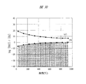
【図13】Ru膜形成時のH2OおよびH2の分圧比を示す図である。
【図14】Ru膜の成膜の反応機構を示す図である。
【図15】本発明の実施の形態1である半導体集積回路装置の製造方法を示す半導体基板の要部断面図である。
【図16】本発明の実施の形態1である半導体集積回路装置の製造方法を示す半導体基板の要部断面図である。
【図17】本発明の実施の形態1である半導体集積回路装置の製造方法を示す半導体基板の要部平面図である。
【図18】本発明の実施の形態2である半導体集積回路装置の製造方法を示す半導体基板の要部断面図である。
【図19】Ru膜形成時のH2OおよびH2の分圧比を示す図である。
【図20】Ru膜形成時のH2OおよびH2の分圧比を示す図である。
【図21】Ru膜形成時のH2OおよびH2の分圧比を示す図である。
【図22】本発明の実施の形態3である半導体集積回路装置の製造方法を示す半導体基板の要部断面図である。
【図23】酸化タンタル膜形成時のH2OおよびH2の分圧比を示す図である。
【図24】酸化タンタル膜形成時のH2OおよびH2の分圧比を示す図である。
【図25】本発明の実施の形態4である半導体集積回路装置の製造方法を示す半導体基板の要部断面図である。
【図26】本発明の実施の形態4である半導体集積回路装置の製造方法を示す半導体基板の要部断面図である。
【図27】本発明の実施の形態4である半導体集積回路装置の製造方法を示す半導体基板の要部断面図である。
【図28】本発明の実施の形態4である半導体集積回路装置の製造方法を示す半導体基板の要部断面図である。
【図29】Cu膜形成時のH2OおよびH2の分圧比を示す図である。
【図30】Cu膜形成時のH2OおよびH2の分圧比を示す図である。
【図31】Cu膜の成膜反応を示す図である。
【図32】本発明の実施の形態4である半導体集積回路装置の製造方法を示す半導体基板の要部断面図である。
【図33】本発明の実施の形態4である半導体集積回路装置の製造方法を示す半導体基板の要部断面図である。
【図34】本発明の実施の形態4である半導体集積回路装置の製造方法を示す半導体基板の要部断面図である。
【図35】本発明の実施の形態4である半導体集積回路装置の製造方法を示す半導体基板の要部断面図である。
【図36】Ru膜の成膜反応を示す図である。
【図37】Ru膜の成膜反応を示す図である。
【符号の説明】
1 半導体基板
2 素子分離
3 p型ウエル
4 酸化シリコン膜
5 ゲート絶縁膜
6 ゲート電極
7 窒化シリコン膜
8 n型半導体領域
9 窒化シリコン膜
10 酸化シリコン膜
11 コンタクトホール
12 コンタクトホール
13 プラグ
14 酸化シリコン膜
15 スルーホール
16 プラグ
17 酸化シリコン膜
18 窒化シリコン膜
19 スルーホール
20 多結晶シリコン膜
21 サイドウォールスペーサ
22 プラグ
23 バリア層
24 酸化シリコン膜
26 ハードマスク
27 孔
29 WN膜
30 Ru膜
30A 下部電極
32 酸化タンタル膜(Ta2O5)
33 上部電極
33a Ru膜
33b W膜
34 層間絶縁膜
230 Ru膜
332 酸化タンタル膜
401 半導体基板
402 素子分離溝
403 p型ウエル
404 n型ウエル
407 酸化シリコン膜
408 ゲート酸化膜
409 ゲート電極
409a 多結晶シリコン膜
409b W膜
410 窒化シリコン膜
411 n-型半導体領域
412 p-型半導体領域
413 サイドウォールスペーサ
414 n+型半導体領域
415 p+型半導体領域
420 パッシベーション膜
BL ビット線
C 情報蓄積用容量素子(キャパシタ)
C1 コンタクトホール
C2 コンタクトホール
C3〜C5 コンタクトホール
D1 銅拡散防止絶縁膜
D2〜D5 銅拡散防止絶縁膜
H1 配線溝用絶縁膜
H1a 窒化シリコン膜
H1b 酸化シリコン膜
H2 配線溝用絶縁膜
H2a 窒化シリコン膜
H2b 酸化シリコン膜
H3〜H5 配線溝用絶縁膜
HM1 配線溝
HM2 配線溝
HM3 配線溝
L 活性領域
M1 第1層配線
M1a バリア層
M1b Cu(銅)膜
M2 第2層配線
M2a バリア層
M2b 銅膜
M3 第3層配線
M4 第4層配線
M5 第5層配線
P1 プラグ
P2 プラグ
P2a バリア層
P2b タングステン膜
P3〜P5 プラグ
Qn nチャネル型MISFET
Qp pチャネル型MISFET
Qs メモリセル選択用MISFET
TH1 層間絶縁膜
TH2 層間絶縁膜
TH3〜TH5 層間絶縁膜[0001]
BACKGROUND OF THE INVENTION
The present invention relates to a semiconductor integrated circuit device and a method for manufacturing the same, and more particularly to a technique that is effective when applied to a method for forming a metal film or metal oxide by a chemical vapor deposition (CVD) method.
[0002]
[Prior art]
Semiconductor elements and wirings constituting the semiconductor integrated circuit device are formed by repeating the formation of conductive films and insulating films, photolithography and patterning for each film. One of the methods for forming these films is a CVD method using a chemical reaction.
[0003]
On the other hand, for example, a DRAM (Dynamic Random Access Memory) has a memory cell selection MISFET and an information storage capacitor element connected in series to the MISFET. The information storage capacitor element is formed by sequentially depositing a conductive layer serving as a lower electrode, a capacitor insulating film, and a conductive layer serving as an upper electrode, and a metal film such as a Ru (ruthenium) film is used for the lower electrode. It is being considered.
[0004]
Such a metal film and a capacitor insulating film can also be formed by a CVD method. For example, in Japanese Patent Laid-Open No. 9-246214, Ru (DMHPD) Three : A method of forming a Ru film by chemical vapor deposition using 2,6-dimethyl-3,5-heptadione ruthenium as a raw material is disclosed.
[0005]
Japanese Patent Application Laid-Open No. 7-86270 discloses SrTiO that becomes a capacitor insulating film by a CVD method using an organic metal as a raw material. Three Techniques for forming are described.
[0006]
[Problems to be solved by the invention]
The inventor has been researching and developing DRAMs, and has been conducting various studies on the configuration and formation method of the information storage capacitor element described above.
[0007]
Along with the miniaturization of semiconductor integrated circuit devices, the formation area of the information storage capacitor element tends to be reduced, making it difficult to secure a desired capacity. Therefore, it is necessary to study electrode materials and capacitive insulating film materials in order to obtain a large capacity with a small area.
[0008]
In view of this, the present inventor employs a Ru film as the lower electrode of the information storage capacitor element, and conducts various studies on its formation method. This platinum group metal such as Ru does not generate a low dielectric constant film such as an oxynitride film even by heat treatment after formation, and since it is a metal, it can be formed thin and increases capacity. It is because it is considered suitable for this.
[0009]
To form a Ru film, for example, ethoxycyclopentadienyl ruthenium (Ru (C 2 H Five OC Five H Four ) 2 ) In tetrahydrofuran and O 2 A formation method by a CVD method using (oxygen) as a raw material is conceivable.
[0010]
However, in such a film formation method using a reaction between an organic compound (ethylcyclopentadienylruthenium) and oxygen, the organic compound and the compound of these and oxygen remain in the Ru film, and the film quality of the Ru film is deteriorated. Let
[0011]
In addition, if high-temperature annealing is performed after the Ru film is formed in order to remove the organic compound in the Ru film, there is a problem that the metal layer formed under the Ru film is oxidized. For example, platinum group metals such as Ru generally have poor adhesion to an insulating film such as silicon oxide, and therefore, a metal layer serving as an adhesive layer is formed between these films to prevent peeling. However, this metal layer reacts with oxygen or the like in the Ru film and is oxidized during the above-described annealing. As a result, there is a problem that a conduction failure occurs between the information storage capacitor element (lower electrode) and the memory cell selection MISFET.
[0012]
An object of the present invention is to provide a technique for improving the quality of a metal film formed by a CVD method, for example, a Ru film constituting a lower electrode of an information storage capacitor element.
[0013]
Another object of the present invention is to improve the characteristics of a semiconductor integrated circuit device having a good metal film by forming it.
[0014]
The above and other objects and novel features of the present invention will be apparent from the description of this specification and the accompanying drawings.
[0015]
[Means for Solving the Problems]
Of the inventions disclosed in the present application, typical ones will be described as follows.
1. The method of manufacturing a semiconductor integrated circuit device according to the present invention includes a metal film on a semiconductor substrate, such as a Ru film constituting a lower electrode of a capacitor, and a compound of this metal, H 2 O and H 2 And forming by a chemical vapor deposition method using a reducing agent such as
2. According to the method of manufacturing a semiconductor integrated circuit device of the present invention, a metal film on a semiconductor substrate, for example, a Ru film constituting a lower electrode of a capacitor, a Cu film constituting a wiring, or the like is formed at a predetermined temperature. Metal compound, H 2 O and H 2 A step of forming by chemical vapor deposition using such a reducing agent. H 2 When using 2 Said H against 2 O partial pressure ratio ([H 2 O] / [H 2 ]) At the above temperature, system 1 (oxide of metal constituting the metal film + H 2 ) And system 2 (metal constituting the metal film + H 2 H when O) is in equilibrium 2 Against H 2 O partial pressure ratio ([H 2 O] eq / [H 2 eq) has a step of forming under smaller conditions.
3. According to the method of manufacturing a semiconductor integrated circuit device of the present invention, a metal oxide film on a semiconductor substrate, for example, a tantalum oxide film serving as a capacitor insulating film (capacitor insulating film) of a capacitor is formed at a predetermined temperature. H, a metal compound 2 O and H 2 A step of forming by chemical vapor deposition using such a reducing agent. H 2 When using 2 Said H against 2 O partial pressure ratio ([H 2 O] / [H 2 ]) At the above temperature, the system 1 (oxide of metal constituting the metal oxide film + H 2 ) And system 2 (metal + H constituting the metal oxide film) 2 H when O) is in equilibrium 2 Against H 2 O partial pressure ratio ([H 2 O] eq / [H 2 eq) has a step of forming under larger conditions. 4). A method for manufacturing a semiconductor integrated circuit device according to the present invention includes a first metal film or a first metal nitride film on a semiconductor substrate, for example, a W film or a WN film serving as an adhesive layer or a barrier layer. A method of manufacturing a semiconductor integrated circuit device having a second metal film (such as a Ru film or a Cu film), wherein the second metal film is formed at a predetermined temperature with the second metal compound, H 2 O and H 2 A step of forming by chemical vapor deposition using such a reducing agent. H 2 When using 2 Said H against 2 O partial pressure ratio ([H 2 O] / [H 2 ]) At system temperature 1 (oxide of the first metal + H 2 ) And system 2 (the first metal + H 2 H when O) is in equilibrium 2 Against H 2 O partial pressure ratio ([H 2 O] eq / [H 2 eq) has a step of forming under smaller conditions. 5. A method for manufacturing a semiconductor integrated circuit device according to the present invention comprises forming a first metal film or a first metal nitride film on a semiconductor substrate, for example, a W film or WN film serving as a barrier layer, or a lower electrode of a capacitor. A method of manufacturing a semiconductor integrated circuit device having a second metal oxide film (such as a tantalum oxide film serving as a capacitor insulating film of a capacitor) on a Ru film or the like, wherein the second metal oxide film is At a temperature, said second metal compound, H 2 O and H 2 A step of forming by chemical vapor deposition using such a reducing agent. H 2 When using 2 Said H against 2 O partial pressure ratio ([H 2 O] / [H 2 ]) At system temperature 1 (oxide of the second metal + H 2 ) And system 2 (second metal + H 2 H when O) is in equilibrium 2 Against H 2 O partial pressure ratio ([H 2 O] eq1 / [H 2 ] eq1) and at system temperature 3 (oxide of the first metal + H 2 ) And system 4 (the first metal + H 2 H when O) is in equilibrium 2 Against H 2 O partial pressure ratio ([H 2 O] eq2 / [H 2 ] eq2) having a step of forming under smaller conditions.
[0016]
DETAILED DESCRIPTION OF THE INVENTION
Hereinafter, embodiments of the present invention will be described in detail with reference to the drawings. Note that components having the same function are denoted by the same reference symbols throughout the drawings for describing the embodiments, and the repetitive description thereof will be omitted.
[0017]
(Embodiment 1)
A method of manufacturing the DRAM of this embodiment will be described in the order of steps with reference to FIGS.
[0018]
First, as shown in FIG. 1,
[0019]
In order to form the
[0020]
Next, B (boron) is ion-implanted into the
[0021]
Next, as shown in FIG. 3, a
[0022]
Next, as shown in FIG. 4, As (arsenic) or P (phosphorus) is ion-implanted into the p-
[0023]
Next, a silicon nitride film 9 (film thickness of 50 nm) and a silicon oxide film 10 (film thickness of about 600 nm) are deposited on the
[0024]
Next, as shown in FIG. 5, plugs 13 are formed inside the contact holes 11 and 12. In order to form the
[0025]
Next, after depositing a silicon oxide film 14 (film thickness of about 150 nm) on the
[0026]
Next, the
[0027]
Next, the bit line BL is formed on the
[0028]
Next, as shown in FIG. 6, a silicon oxide film 17 (having a film thickness of about 300 nm) is deposited on the upper portion of the bit line BL by a CVD method, and then the surface thereof is flattened by a chemical mechanical polishing method. Next, a silicon nitride film 18 (film thickness of about 50 nm) is deposited on the
[0029]
Next, the
[0030]
The through
[0031]
Next, after the
[0032]
Next, as shown in FIG. 8, the
[0033]
Thereafter, an information storage capacitor element (capacitor) C comprising a
[0034]
The process of forming the information storage capacitive element C will be described in detail with reference to FIGS. These figures are diagrams schematically showing a region where the information storage capacitor element C is to be formed on the
[0035]
As shown in FIG. 9, a
[0036]
Next, a
[0037]
Next, as shown in FIG. 10, a photoresist film (not shown) is formed on the
[0038]
Next, after removing the
[0039]
Next, as shown in FIG. 12, a Ru film 30 (film thickness of about 30 nm) is deposited on the
[0040]
This
[0041]
This Ru (HFAC) Three The organic compound solution of 2 O and H 2 To form a film. An example of the organic compound solution is a tetrahydrofuran solution. Where H 2 O and H 2 The reaction is caused to occur while controlling the partial pressure ratio so as to be located in the region below the graph (a) shown in FIG.
[0042]
First, the reaction mechanism for forming this Ru film will be described. As the reaction mechanism, the mechanism shown in FIG. 14 can be considered. As shown in FIG. 14, Ru (HFAC) Three First, H 2 Reacts with O (H 2 Decomposed by O) and hydroxide Ru (OH) Three (FIG. 14A). This hydroxide Ru (OH) Three Is reduced by hydrogen to produce Ru (FIG. 14B). As is clear from this reaction mechanism, H 2 O is not consumed and acts as a catalyst. In addition, since the reaction chamber in which the reaction is performed is exhausted, Ru (HFAC) which is a substantial raw material Three And H 2 Like H 2 O also needs to be supplied as appropriate.
[0043]
Thus, according to the present embodiment, Ru (HFAC) Three , H 2 O and H 2 As a Ru film is formed by utilizing hydrolysis, a Ru film with good film quality can be formed.
[0044]
For example, ethoxycyclopentadienyl ruthenium (Ru (C 2 H Five OC Five H Four ) 2 The organic compound solution of Ru such as a tetrahydrofuran solution of 2 It is also possible to form a Ru film by reacting with. However, in this case, it is a reaction that generates Ru by causing incomplete combustion so that Ru is not oxidized. As a result, in addition to carbon, hydrogen, or these oxygen compounds, organic compounds and oxides thereof generated during the reaction are incorporated into the Ru film, which causes the quality of the Ru film to deteriorate. Further, the heat treatment performed thereafter, for example, the heat treatment for densification (densification) of the Ru film vaporizes carbon, hydrogen, or these oxygen compounds incorporated into the Ru film, and the quality of the Ru film is improved. Deteriorate. Also, oxygen and oxygen compounds in the Ru film oxidize the
[0045]
On the other hand, according to the present embodiment, Ru (HFAC) Three Since the Ru film was generated by utilizing hydrolysis of, by-products such as carbon and hydrogen or these compounds incorporated into the Ru film can be reduced. That is, since a Ru film having good crystallinity can be formed, carbon or hydrogen incorporated into the Ru film by a heat treatment performed later, for example, a heat treatment for densification (densification) of the Ru film, or the like. Even if these oxygen compounds are vaporized, the vaporization amount is small and the quality of the Ru film can be maintained. Further, even during the heat treatment of the capacitive insulating film formed on the lower electrode (Ru film 30), which will be described later, film shrinkage due to vaporization of carbon or the like in the Ru film can be reduced, and damage to the capacitive insulating film can be prevented. it can. As a result, the characteristics of the information storage capacitive element C can be improved. In addition, the amount of oxygen and oxygen compounds in the Ru film can be reduced, and poor conduction between the
[0046]
H 2 O and H 2 The reason why the partial pressure ratio is controlled to be located in the region below the graph (a) shown in FIG. 13 is to suppress the oxidation of Ru during the formation of the Ru film. That is, when the Ru film is formed, the generated Ru and H 2 RuO reacts with O 2 A side reaction of (ruthenium oxide) may occur. The reason why this reaction (Ru oxidation) can be suppressed will be described below.
[0047]
The graph (a) in FIG. 13 shows system 1 (RuO 2 + H 2 ) And system 2 (Ru + H) 2 The logarithm of the equilibrium constant k in the equilibrium state with O) is expressed with respect to the reaction temperature. Logk = log [[H 2 O] eq / [H 2 ] eq] ([H 2 O] eq: H in equilibrium 2 O partial pressure, [H 2 ] eq: H in equilibrium 2 (Partial pressure). Further, the equilibrium constant k can be obtained from ΔG = −RTlnk by the difference (ΔG) in the cast free energy between the
[0048]
Therefore, under the condition located in the region above the graph (a), the equilibrium moves in the direction in which Ru is oxidized. However, H 2 O and H 2 The Ru oxidation can be suppressed by forming the Ru film while controlling the partial pressure ratio so that it is located in the region below the graph (a) shown in FIG.
[0049]
However, Ru (HFAC), which is a raw material, is used for forming a Ru film. Three Since it is necessary to vaporize the solution and the raw material may decompose when treated at a too high temperature, the reaction temperature seems to be preferably about 100 to 200 ° C. (above the boiling point of the raw material solution) to about 500 ° C.
[0050]
Thus, according to the present embodiment, Ru (HFAC) Three , H 2 O and H 2 In addition, H 2 O and H 2 Since the reaction was caused to be controlled so that the partial pressure ratio is located in the region below the graph (a) shown in FIG. 13, the content of oxygen, carbon, or these compounds is low while preventing the oxidation of the Ru film. A good Ru film can be formed.
[0051]
Next, heat treatment is performed at 700 ° C. for 1 minute to densify (densify) the
[0052]
Next, as shown in FIG. 15, a photoresist film (not shown) is applied on the
[0053]
Next, a
[0054]
Next, as shown in FIG. 16, the
[0055]
Through the steps up to here, the information storage capacitor element C constituted by the
[0056]
Thereafter, an
[0057]
As described above in detail, according to the present embodiment, Ru (HFAC) Three Since the Ru film was generated by utilizing hydrolysis of the by-product, by-products incorporated into the Ru film can be reduced, and the film quality of the Ru film can be improved.
[0058]
In the present embodiment, H used for forming the Ru film is also used. 2 O and H 2 Is controlled so as to be located in a region below the graph (a) shown in FIG. 13, Ru oxidation can be suppressed during the formation of the Ru film.
[0059]
As a result, the characteristics of the information storage capacitive element C can be improved, and the characteristics of the memory cell can be improved. In addition, a desired capacity can be secured even in a miniaturized memory cell structure.
[0060]
(Embodiment 2)
In the first embodiment, Ru (HFAC) Three , H 2 O and H 2 As a raw material, H 2 O and H 2
[0061]
Hereinafter, a method of manufacturing the DRAM of this embodiment will be described. Note that the process up to the formation of the
[0062]
As shown in FIG. 18, a Ru film (not shown) having a thickness of about 15 nm is formed on the
[0063]
Here, the
[0064]
The graph (a) in FIG. 19 shows system 1 (RuO 2 + H 2 ) And system 2 (Ru + H) 2 The logarithm of the equilibrium constant k in the equilibrium state with O) is expressed with respect to the reaction temperature, and the graph (b) shows the system 1 (WO 2 + H 2 ) And system 2 (W + H) 2 The logarithm of the equilibrium constant k in the equilibrium state with O) is expressed with respect to the reaction temperature. As described in the first embodiment, this logk = log [[H 2 O] eq / [H 2 ] eq] ([H 2 O] eq: H in equilibrium 2 O partial pressure, [H 2 ] eq: H in equilibrium 2 This equilibrium constant k can be obtained from the difference in the free energy of the cast between the
[0065]
Therefore, under the condition located in the region above the graph (b), the equilibrium moves in the direction in which W is oxidized. However, H 2 O and H 2 When the Ru film is formed while controlling the partial pressure ratio so as to be located in the region below the graph (b) shown in FIG. 19, it is possible to suppress oxidation of W while suppressing oxidation of Ru.
[0066]
As a result, in addition to the effects described in the first embodiment, oxidation of W in the
[0067]
Next, heat treatment is performed at 700 ° C. for 1 minute to densify (densify) the
[0068]
Since the subsequent steps are the same as those in the first embodiment described with reference to FIGS. 15 and 16, the description thereof will be omitted.
[0069]
As described in detail above, according to the present embodiment, the
[0070]
In the first and second embodiments, the Ru film has been described as an example. However, an Ir (iridium) film, Pd (palladium), Pt (platinum), or the like also forms hexafluoroacetylacetone and a complex compound (acetylacetonate derivative). These complex compounds, H 2 O and H 2 As a raw material, and as in
[0071]
(Embodiment 3)
In the first and second embodiments, H during Ru film formation 2 O and H 2 Was controlled, but the tantalum oxide film (Ta 2 O Five ) H as explained below 2 O and H 2 The partial pressure ratio may be controlled.
[0072]
Hereinafter, a method of manufacturing the DRAM of this embodiment will be described. The steps up to the formation of the
[0073]
As shown in FIG. 22, a
[0074]
Thus, according to the present embodiment, pentaethoxytantalum (Ta (OC 2 H Five ) Five ) And H 2 Since the
[0075]
That is, as described in
[0076]
In contrast, according to the present embodiment, pentaethoxytantalum (Ta (OC 2 H Five ) Five ) Is used to generate a
[0077]
Pentaethoxytantalum (Ta (OC 2 H Five ) Five ) And H 2 O and H 2 The
[0078]
That is, H 2 O and H 2 The reaction is caused to occur while controlling the partial pressure ratio so as to be located in the region surrounded by the graphs (a) and (c) shown in FIG.
[0079]
The graph (c) in FIG. 23 shows the system 1 (Ta 2 O Five + H 2 ) And system 2 (Ta + H) 2 The logarithm of the equilibrium constant k in the equilibrium state with O) is expressed with respect to the reaction temperature. As described in the first embodiment, this logk = log [[H 2 O] eq / [H 2 ] eq] ([H 2 O] eq: H in equilibrium 2 O partial pressure, [H 2 ] eq: H in equilibrium 2 This equilibrium constant k can be obtained from the difference in the free energy of the cast between the
[0080]
Therefore, under the condition located in the region below the graph (c), Ta 2 O Five In order to form the
[0081]
Thus, according to the present embodiment, pentaethoxytantalum (Ta (OC 2 H Five ) Five ), H 2 O and H 2 In addition, H 2 O and H 2 Since the reaction was caused to be controlled so as to be positioned in the region surrounded by the graphs (a) and (c) shown in FIG. 23, the oxidation of the Ru film was prevented and the
[0082]
H 2 O and H 2 When the reaction is caused to occur while controlling the partial pressure ratio of the Ru film and the WN film as described in the second embodiment, the control is performed so as to be positioned in the region surrounded by the graphs (b) and (c) shown in FIG. The
[0083]
Next, heat treatment is performed at 650 ° C. in an Ar (argon) atmosphere to crystallize the
[0084]
Next, as in the first embodiment, the
[0085]
As described above in detail, according to this embodiment, pentaethoxytantalum (Ta (OC 2 H Five ) Five ), H 2 O and H 2 In addition, H 2 O and H 2 Therefore, the
[0086]
Therefore, poor conduction between the Ru film 30 (lower electrode) and the
[0087]
In this embodiment, a tantalum oxide film is used as the capacitor insulating film. 2 O Three And BST (Ba X Sr 1-X TiO Three ) May be used.
[0088]
Al (CH Three ) 2 H (dimethylaluminum hydride), H 2 O and H 2 As a raw material, and as in this embodiment, H 2 O and H 2 While controlling the partial pressure ratio of Al 2 O Three If a film is formed, the same effect can be obtained.
[0089]
Also, the BST film is made of Ba (C (CH Three ) Three -CO-CH-CO-C (CH Three ) Three ) 2 bis (dipivaloylmetanate) barium, Sr (C (CH Three ) Three -CO-CH-CO-C (CH Three ) Three ) 2 bis (dipivaloylmetanate) strontium or TiO (C (CH Three ) Three -CO-CH-CO-C (CH Three ) Three ) 2 titanylbis (dipivaloylmetanate) and H 2 O and H 2 Can be formed as a raw material, and in this case as well, in this embodiment, H 2 O and H 2 The same effect can be obtained if the BST film is formed while controlling the partial pressure ratio.
[0090]
In the first to third embodiments, the DRAM memory cell has been described as an example. However, the present invention is not limited to the DRAM, and the present invention can be widely applied to semiconductor integrated circuits having MIM (Metal Insulator Metal) capacitors.
[0091]
(Embodiment 4)
In the first to third embodiments, the present invention is applied to the information storage capacitive element portion of the DRAM. However, the present invention may be applied to the wiring portion. Next, a method for manufacturing a semiconductor integrated circuit device according to an embodiment of the present invention will be described. 25 to 28 and FIGS. 32 to 35 are cross-sectional views of relevant parts of the substrate showing the method of manufacturing the semiconductor integrated circuit device according to the embodiment of the present invention.
[0092]
First, as shown in FIG. 25, an n-channel MISFET Qn and a p-channel MISFET Qp are formed by a normal MISFET formation process.
[0093]
Examples of normal MISFET formation processes include the following.
[0094]
First, an
[0095]
Next, after p-type impurities and n-type impurities are ion-implanted into the
[0096]
Next, a low-resistance
[0097]
Next, the
[0098]
Next, n-type impurities are ion-implanted into the p-type well 403 on both sides of the
[0099]
Next, after depositing a silicon nitride film on the
[0100]
Next, an n-type impurity is ion-implanted into the p-type well 403 to form n + Type semiconductor region 414 (source, drain) is formed, and p-type impurities are ion-implanted into n-type well 404 to form p + A type semiconductor region 415 (source, drain) is formed.
[0101]
Through the steps up to here, an n-channel MISFET Qn and a p-channel MISFET Qp having a source and a drain having an LDD (Lightly Doped Drain) structure are formed.
[0102]
Thereafter, an interlayer insulating film such as a silicon oxide film and a conductive film such as a copper film are alternately deposited on the MISFETs Qn and Qp to form a plurality of wirings. This will be described in detail with reference to FIGS.
[0103]
First, as shown in FIG. 26, a silicon oxide film having a thickness of about 700 nm to 800 nm is deposited on the MISFETs Qn and Qp by the CVD method, and then the silicon oxide film is polished by the chemical mechanical polishing method to flatten the surface. Thus, the interlayer insulating film TH1 is formed.
[0104]
Next, a photoresist film is formed on the interlayer insulating film TH1 (not shown), and the interlayer insulating film TH1 is etched using this photoresist film as a mask, thereby forming n on the main surface of the
[0105]
Next, as shown in FIG. 27, a tungsten film is deposited by CVD on the interlayer insulating film TH1 including the inside of the contact hole C1, and this tungsten film is polished by chemical mechanical polishing until the interlayer insulating film TH1 is exposed. Thus, the plug P1 is formed in the contact hole C1. Note that a thin TiN film may be deposited before the tungsten film is deposited, and the plug P1 may have a laminated structure of a barrier film made of a TiN film or the like and a tungsten film.
[0106]
Next, a silicon nitride film H1a and a silicon oxide film H1b are sequentially deposited on the interlayer insulating film TH1 and the plug P1 by a CVD method to form a wiring trench insulating film H1 made of these films. The wiring groove HM1 is formed by etching the wiring groove insulating film H1 in the first layer wiring formation scheduled region. The silicon nitride film H1a is used as an etching stopper during the etching.
[0107]
Next, as shown in FIG. 28, a barrier layer M1a made of tungsten nitride is deposited by sputtering on the wiring groove insulating film H1 including the inside of the wiring groove HM1, and then a copper film M1b is formed on the barrier layer M1a. It is formed by the CVD method.
[0108]
This copper film M1b is made of Cu (HFAC) which is a compound of Cu (copper). 2 , H 2 O and H 2 Is used as a raw material. HFAC is (CF Three COCHCOCF Three ) - Means.
[0109]
This Cu (HFAC) 2 The organic compound solution of 2 O and H 2 To form a film. An example of the organic compound solution is a tetrahydrofuran solution. Where H 2 O and H 2 The reaction is caused to occur while controlling the partial pressure ratio in the region below the graph (a ′) shown in FIG.
[0110]
The reason for controlling in this way is to suppress Cu oxidation during the formation of the Cu film. The reason why the oxidation of Cu can be suppressed can also be explained as in the case of Ru.
[0111]
That is, this FIG. 29 shows the system 1 (CuO + H 2 ) And system 2 (Cu + H) 2 The logarithm of the equilibrium constant k in the equilibrium state with O) is expressed with respect to the reaction temperature. Logk = log [[H 2 O] eq / [H 2 ] eq] ([H 2 O] eq: H in equilibrium 2 O partial pressure, [H 2 ] eq: H in equilibrium 2 (Partial pressure). Further, the equilibrium constant k can be obtained from ΔG = −RTlnk by the difference (ΔG) in the cast free energy between the
[0112]
Therefore, under the condition located in the region above the graph (a ′), the equilibrium moves in the direction in which Cu is oxidized. However, H 2 O and H 2 When the Cu film is formed while controlling the partial pressure ratio so that it is located in the region below the graph (a ′) shown in FIG. 29, the oxidation of Cu can be suppressed.
[0113]
However, Cu (HFAC) which is a raw material is used for forming a Cu film. 2 Since it is necessary to vaporize the solution and the decomposition of the raw material may occur if the solution is treated at a too high temperature, the reaction temperature seems to be preferably about 100 to 200 ° C. (above the boiling point of the raw material solution) to about 500 ° C.
[0114]
Thus, according to the present embodiment, Cu (HFAC) 2 , H 2 O and H 2 In addition, H 2 O and H 2 Since the reaction was caused to be controlled so as to be located in a region below the graph (a ′) shown in FIG. 29, the content of oxygen, carbon, or these compounds was prevented while preventing the oxidation of the Cu film. A few good Cu films can be formed.
[0115]
Further, this Cu film M1b is made to be H 2 O and
[0116]
Graph (b) in FIG. 30 shows system 1 (WO 2 + H 2 ) And system 2 (W + H) 2 The logarithm of the equilibrium constant k in the equilibrium state with O) is expressed with respect to the reaction temperature. As described above, this logk = log [[H 2 O] eq / [H 2 ] eq] ([H 2 O] eq: H in equilibrium 2 O partial pressure, [H 2 ] eq: H in equilibrium 2 This equilibrium constant k can be obtained from the difference in the free energy of the cast between the
[0117]
Therefore, under the condition located in the region above the graph (b), the equilibrium moves in the direction in which W is oxidized. However, H 2 O and H 2 When the Cu film is formed while controlling the partial pressure ratio so that it is located in the region below the graph (b) shown in FIG. 30, the oxidation of W can be suppressed while suppressing the oxidation of Cu.
[0118]
Therefore, oxidation of Cu in the film formation and W in the barrier layer M1a made of tungsten nitride can be suppressed. As a result, poor conduction between the Cu film M1b and the plug P1 can be prevented. Further, by suppressing the oxidation of W in the barrier layer M1a, it is possible to prevent a decrease in barrier properties. As a result, a short circuit between wirings due to diffusion of Cu into the insulating film can be prevented.
[0119]
The copper film M1b was formed by using a Cu cation and hexafluoroacetylacetone (CF Three COCHCOCF Three ) - And trimethylvinylsilane (CH 2 CHSi (CH Three ) Three ) Cu (HFAC) (TMVS), H 2 O and H 2 May be formed as a raw material. HFAC is (CF Three COCHCOCF Three ) - TMVS is (CH 2 = CHSi (CH Three ) Three ).
[0120]
The organic compound solution of Cu (HFAC) (TMVS) is vaporized, and H 2 O and H 2 To form a film. An example of the organic compound solution is a tetrahydrofuran solution. The reaction of forming the Cu film is shown in FIG. Even in this reaction, H 2 O acts as a catalyst and H 2 The reaction rate increases by adding O.
[0121]
In this reaction, as described above, H 2 O and H 2 If the partial pressure ratio is controlled to be in a region below the graph (a ′) shown in FIG. 29, Cu oxidation can be suppressed. H 2 O and
[0122]
Next, as shown in FIG. 32, the copper film M1b and the barrier layer M1a outside the wiring trench HM1 are removed by a chemical mechanical polishing method to form a first layer wiring M1 composed of the copper film M1b and the barrier layer M1a.
[0123]
Next, as shown in FIG. 33, an insulating film D1 for preventing copper diffusion is formed on the first layer wiring M1 by depositing a silicon nitride film by a CVD method, and then an interlayer insulating film TH2 is formed. The interlayer insulating film TH2 is formed in the same manner as the interlayer insulating film TH1.
[0124]
Next, a resist film (not shown) having an opening in the contact region of the first layer wiring M1 is formed on the interlayer insulating film TH2, and this is used as a mask until the surface of the first layer wiring M1 is exposed. The film TH2 and the copper diffusion preventing insulating film D1 are anisotropically etched.
[0125]
Next, as shown in FIG. 34, a barrier layer P2a is formed by depositing 30 to 70 nm of a refractory metal nitride such as TiN on the interlayer insulating film TH2 including the inside of the contact hole C2. Next, a tungsten film P2b of about 200 to 500 nm is deposited on the barrier layer P2a by a CVD method. The tungsten film P2b is formed so as to completely fill the contact hole C2.
[0126]
Subsequently, the tungsten film P2b and the barrier layer P2a outside the contact hole C2 are removed by chemical mechanical polishing to form a plug P2 composed of the tungsten film P2b and the barrier layer P2a.
[0127]
Next, as shown in FIG. 35, the second layer wiring M2 is formed on the plug P2 in the same manner as the first layer wiring M1. That is, the silicon nitride film H2a and the silicon oxide film H2b are sequentially deposited on the interlayer insulating film TH2 and the plug P2, and the wiring groove HM2 is formed by etching the wiring groove insulating film H2 made of these films. Next, a barrier layer M2a made of titanium nitride is deposited on the wiring groove insulating film H2 including the inside of the wiring groove HM2, and then a copper film M2b is formed on the barrier layer M2a by the CVD method under the above-described conditions. Next, the copper film M2b and the barrier layer M2a outside the wiring trench HM2 are removed by chemical mechanical polishing to form the second layer wiring M2 composed of the copper film M2b and the barrier layer M2a.
[0128]
Next, a copper diffusion preventing insulating film D2 and an interlayer insulating film TH3 are formed on the second layer wiring M2. These films are formed in the same manner as the copper diffusion preventing insulating film D1 and the interlayer insulating film TH1. Thereafter, a contact hole C3 is formed in the copper diffusion preventing insulating film D2 and the interlayer insulating film TH3, and a plug P3 is formed in the contact hole C3. The plug P3 is formed in the same manner as the plug P2. Next, the wiring groove insulating film H3 and the wiring groove HM3 are formed on the interlayer insulating film TH3 and the plug P3 in the same manner as the wiring groove insulating film H1 and the wiring groove HM1, and the third layer wiring M1 is formed as in the first layer wiring M1. A layer wiring M3 is formed.
[0129]
Formation of copper diffusion preventing insulating films (D3, D4, D5) and interlayer insulating films (TH4, TH5) on this wiring, formation of plugs (P4, P5) formed in contact holes in these films, and on the plugs By repeating the formation of the wirings (M4, M5), a semiconductor integrated circuit device having a multilayer wiring structure can be formed.
[0130]
Subsequently, a
[0131]
Thereafter, the semiconductor integrated circuit device is completed by being mounted on a package substrate or the like, but the description thereof is omitted.
[0132]
In this embodiment, five layers of wiring are formed, but five layers or less or five layers or more may be formed. In the present embodiment, MISFETs Qn and Qp are formed as semiconductor elements. However, the present invention is not limited to these MISFETs, and other elements such as bipolar transistors can be formed. Further, the present invention can be widely applied to semiconductor integrated circuit devices having metal wirings formed by a CVD method.
[0133]
(Embodiment 5)
In the first embodiment, H is formed when the Ru film is formed. 2 O and H 2 Although the partial pressure ratio was controlled, this membrane was 2 Alternatively, the film may be formed using alcohol.
[0134]
Hereinafter, a method for manufacturing the DRAM of the present embodiment will be described. At the time of forming the Ru film, H as a reducing agent is used. 2 Since the process is the same as that of the first embodiment except that alcohol is used instead of the above, only the Ru film forming process will be described below.
[0135]
For example, a Ru film (not shown) having a film thickness of about 15 nm is formed on the
[0136]
Here, this
[0137]
First, the reaction mechanism for forming this Ru film will be described. Ru (HFAC) Three First, H 2 Reacts with O (H 2 Decomposed by O) and hydroxide Ru (OH) Three It becomes. This hydroxide Ru (OH) Three Is reduced by alcohol (R—OH) to produce Ru. At this time, the alcohol is oxidized to an aldehyde or a ketone.
[0138]
FIG. 36 shows the reaction mechanism when isopropyl alcohol is used. Ru (HFAC) Three Ru (DPM) instead of Three May be used (FIG. 37). Here, DPM is ((CH Three ) Three CCOCHCOC (CH Three ) Three ) - Means. Such a reaction is an exothermic reaction of about 68 kJ at room temperature and atmospheric pressure, and proceeds easily.
[0139]
Thus, according to the present embodiment, Ru (HFAC) Three , H 2 Since the Ru film is formed by hydrolysis using O and alcohol, as described in the first embodiment, it is possible to form a Ru film with good film quality.
[0140]
Furthermore, alcohol is H 2 Since it is easier to handle than this, a Ru film can be formed easily.
[0141]
In this embodiment, the Ru film has been described as an example, but the Ir compound, H 2 If an Ir film is formed using O and alcohol as raw materials, the same effect can be obtained.
[0142]
Further, the Cu film constituting the wiring described in the fourth embodiment is replaced with a Cu compound, H 2 If O and alcohol are used as raw materials, the same effect can be obtained. A method of manufacturing a semiconductor integrated circuit device having a Cu film in the wiring portion is also used as a reducing agent. 2 Since it is the same as that of the case of
[0143]
As mentioned above, the invention made by the present inventor has been specifically described based on the embodiment. However, the present invention is not limited to the embodiment, and various modifications can be made without departing from the scope of the invention. Needless to say.
[0144]
【The invention's effect】
The effects obtained by the representative ones of the inventions disclosed by the present application will be briefly described as follows.
[0145]
The film quality of a metal film formed by the CVD method, for example, a Ru film constituting the lower electrode of the information storage capacitor element or a Cu film constituting the wiring can be improved.
[0146]
Further, it is possible to improve the film quality of a metal oxide film formed by a CVD method, for example, a tantalum oxide film constituting a capacitor insulating film of an information storage capacitor element.
[0147]
In addition, the oxidation of the metal film and the metal nitride film located under the metal film and the metal oxide film formed by the CVD method can be suppressed, and the conduction failure can be reduced.
[0148]
As a result, the characteristics of the semiconductor integrated circuit device can be improved.
[Brief description of the drawings]
FIG. 1 is a fragmentary cross-sectional view of a semiconductor substrate showing a method for manufacturing a semiconductor integrated circuit device according to a first embodiment of the present invention;
FIG. 2 is a plan view of the essential part of the semiconductor substrate showing the method of manufacturing the semiconductor integrated circuit device which is
3 is a fragmentary cross-sectional view of the semiconductor substrate showing the method of manufacturing the semiconductor integrated circuit device which is
4 is a fragmentary cross-sectional view of the semiconductor substrate showing the method of manufacturing the semiconductor integrated circuit device which is
FIG. 5 is a fragmentary cross-sectional view of the semiconductor substrate showing the method of manufacturing the semiconductor integrated circuit device which is
6 is a fragmentary cross-sectional view of the semiconductor substrate showing the method of manufacturing the semiconductor integrated circuit device which is
FIG. 7 is a fragmentary cross-sectional view of the semiconductor substrate showing the method of manufacturing the semiconductor integrated circuit device which is
FIG. 8 is a fragmentary cross-sectional view of the semiconductor substrate showing the method of manufacturing the semiconductor integrated circuit device which is
FIG. 9 is a fragmentary cross-sectional view of the semiconductor substrate showing the method of manufacturing the semiconductor integrated circuit device which is
FIG. 10 is a fragmentary cross-sectional view of the semiconductor substrate showing the method of manufacturing the semiconductor integrated circuit device which is
FIG. 11 is a fragmentary cross-sectional view of the semiconductor substrate showing the method of manufacturing the semiconductor integrated circuit device which is
FIG. 12 is a fragmentary cross-sectional view of the semiconductor substrate showing the method of manufacturing the semiconductor integrated circuit device which is
FIG. 13 shows H during Ru film formation. 2 O and H 2 It is a figure which shows the partial pressure ratio.
FIG. 14 is a diagram showing a reaction mechanism for forming a Ru film.
FIG. 15 is a fragmentary cross-sectional view of the semiconductor substrate showing the method of manufacturing the semiconductor integrated circuit device which is
FIG. 16 is a fragmentary cross-sectional view of the semiconductor substrate showing the method of manufacturing the semiconductor integrated circuit device which is
FIG. 17 is a substantial part plan view of the semiconductor substrate, illustrating the method for manufacturing the semiconductor integrated circuit device which is
FIG. 18 is a fragmentary cross-sectional view of the semiconductor substrate showing the method of manufacturing the semiconductor integrated circuit device which is
FIG. 19 shows H during Ru film formation. 2 O and H 2 It is a figure which shows the partial pressure ratio.
FIG. 20 shows H during Ru film formation. 2 O and H 2 It is a figure which shows the partial pressure ratio.
FIG. 21 shows H during Ru film formation. 2 O and H 2 It is a figure which shows the partial pressure ratio.
FIG. 22 is a fragmentary cross-sectional view of the semiconductor substrate showing the method of manufacturing the semiconductor integrated circuit device which is
FIG. 23 shows H during tantalum oxide film formation. 2 O and H 2 It is a figure which shows the partial pressure ratio.
FIG. 24 shows H during tantalum oxide film formation. 2 O and H 2 It is a figure which shows the partial pressure ratio.
FIG. 25 is a fragmentary cross-sectional view of the semiconductor substrate showing the method of manufacturing the semiconductor integrated circuit device which is
FIG. 26 is a fragmentary cross-sectional view of the semiconductor substrate showing the method of manufacturing the semiconductor integrated circuit device which is
FIG. 27 is a fragmentary cross-sectional view of the semiconductor substrate showing the method of manufacturing the semiconductor integrated circuit device which is
FIG. 28 is a fragmentary cross-sectional view of a semiconductor substrate showing a method of manufacturing a semiconductor integrated circuit device according to
FIG. 29 shows H during Cu film formation. 2 O and H 2 It is a figure which shows the partial pressure ratio.
FIG. 30 shows H during Cu film formation. 2 O and H 2 It is a figure which shows the partial pressure ratio.
FIG. 31 is a diagram showing a film formation reaction of a Cu film.
FIG. 32 is a cross sectional view for a main portion of the semiconductor substrate showing the method for manufacturing the semiconductor integrated circuit device which is
FIG. 33 is a fragmentary cross-sectional view of the semiconductor substrate showing the method of manufacturing the semiconductor integrated circuit device which is
34 is a fragmentary cross-sectional view of the semiconductor substrate showing the method of manufacturing the semiconductor integrated circuit device which is
FIG. 35 is a cross sectional view for a main portion of the semiconductor substrate, showing a method for manufacturing the semiconductor integrated circuit device which is
FIG. 36 is a diagram showing a film formation reaction of a Ru film.
FIG. 37 is a diagram showing a film formation reaction of a Ru film.
[Explanation of symbols]
1 Semiconductor substrate
2 element isolation
3 p-type well
4 Silicon oxide film
5 Gate insulation film
6 Gate electrode
7 Silicon nitride film
8 n-type semiconductor region
9 Silicon nitride film
10 Silicon oxide film
11 Contact hole
12 Contact hole
13 plugs
14 Silicon oxide film
15 Through hole
16 plug
17 Silicon oxide film
18 Silicon nitride film
19 Through hole
20 Polycrystalline silicon film
21 Sidewall spacer
22 plug
23 Barrier layer
24 Silicon oxide film
26 hard mask
27 holes
29 WN film
30 Ru membrane
30A Lower electrode
32 Tantalum oxide film (Ta 2 O Five )
33 Upper electrode
33a Ru membrane
33b W film
34 Interlayer insulation film
230 Ru membrane
332 Tantalum oxide film
401 Semiconductor substrate
402 Element isolation groove
403 p-type well
404 n-type well
407 Silicon oxide film
408 Gate oxide film
409 Gate electrode
409a polycrystalline silicon film
409b W film
410 Silicon nitride film
411 n - Type semiconductor region
412 p - Type semiconductor region
413 Side wall spacer
414 n + Type semiconductor region
415 p + Type semiconductor region
420 Passivation film
BL bit line
C Information storage capacitor (capacitor)
C1 contact hole
C2 contact hole
C3-C5 contact hole
D1 Copper diffusion prevention insulating film
D2-D5 Copper diffusion prevention insulating film
H1 Insulation film for wiring trench
H1a silicon nitride film
H1b silicon oxide film
H2 Insulation film for wiring trench
H2a silicon nitride film
H2b silicon oxide film
H3-H5 Insulation film for wiring trench
HM1 wiring groove
HM2 wiring groove
HM3 wiring groove
L Active region
M1 first layer wiring
M1a barrier layer
M1b Cu (copper) film
M2 Second layer wiring
M2a barrier layer
M2b copper film
M3 3rd layer wiring
M4 4th layer wiring
M5 5th layer wiring
P1 plug
P2 plug
P2a barrier layer
P2b tungsten film
P3-P5 plug
Qn n-channel MISFET
Qp p-channel MISFET
Qs MISFET for memory cell selection
TH1 interlayer insulation film
TH2 interlayer insulation film
TH3-TH5 interlayer insulation film
Claims (17)
(b)前記メモリセル選択用MISFETのソース、ドレイン領域と電気的に接続するプラグを形成する工程と、
(c)前記プラグに接続するキャパシタの下部電極を構成するRu(ルテニウム)膜を、Ruの化合物、H2OおよびH2もしくはアルコールを原料として使用し、化学気相成長法で前記Ru膜を形成する工程と、
を有し、
前記Ruの化合物は、Ruのアセチルアセトン誘導体化合物であることを特徴とする半導体集積回路装置の製造方法。(A) forming a memory cell selecting MISFET on the main surface of the semiconductor substrate;
(B) forming a plug electrically connected to the source and drain regions of the memory cell selection MISFET;
(C) A Ru (ruthenium) film constituting a lower electrode of a capacitor connected to the plug is used as a raw material with a Ru compound, H 2 O and H 2 or alcohol, and the Ru film is formed by chemical vapor deposition. Forming, and
I have a,
The method of manufacturing a semiconductor integrated circuit device, wherein the Ru compound is a Ru acetylacetone derivative compound .
(d)前記Ru膜上に容量絶縁膜を形成する工程と、
(e)前記容量絶縁膜上に上部電極を形成する工程と、
を有することを特徴とする請求項1記載の半導体集積回路装置の製造方法。The method for manufacturing the semiconductor integrated circuit device further includes:
(D) forming a capacitive insulating film on the Ru film;
(E) forming an upper electrode on the capacitive insulating film;
2. The method of manufacturing a semiconductor integrated circuit device according to claim 1, further comprising:
(b)前記メモリセル選択用MISFETのソース、ドレイン領域と電気的に接続するプラグを形成する工程と、
(c)前記プラグに接続するキャパシタの下部電極を構成するRu(ルテニウム)膜を、Ruの化合物、H2OおよびH2を原料として使用し、化学気相成長法により、所定の温度でRu膜を形成する工程とを有し、
前記温度における前記H2に対する前記H2Oの分圧比([H2O]/[H2])が、前記温度において系1(RuO2+H2)と系2(Ru+H2O)が平衡状態となる際のH2に対するH2Oの分圧比([H2O]eq/[H2]eq)より小さくなる条件下で前記Ru膜が形成され、
前記Ruの化合物は、Ruのアセチルアセトン誘導体化合物であることを特徴とする半導体集積回路装置の製造方法。(A) forming a memory cell selecting MISFET on the main surface of the semiconductor substrate;
(B) forming a plug electrically connected to the source and drain regions of the memory cell selection MISFET;
(C) A Ru (ruthenium) film constituting the lower electrode of the capacitor connected to the plug is made of Ru compound, H 2 O and H 2 as raw materials, and is subjected to Ru at a predetermined temperature by chemical vapor deposition. Forming a film,
The partial pressure ratio of the H 2 O to the H 2 at the temperature ([H 2 O] / [H 2 ]) indicates that the system 1 (RuO 2 + H 2 ) and the system 2 (Ru + H 2 O) are in an equilibrium state at the temperature. the Ru film at a partial pressure ratio ([H 2 O] eq / [H 2] eq) becomes smaller than the conditions of H 2 O is formed to H 2 at the time of the,
The method of manufacturing a semiconductor integrated circuit device, wherein the Ru compound is a Ru acetylacetone derivative compound .
(b)前記メモリセル選択用MISFETのソース、ドレイン領域と電気的に接続されたプラグを形成する工程と、
(c)前記プラグ上に酸化シリコン膜を形成する工程と、
(d)前記酸化シリコン膜中に前記プラグ表面を露出する孔を形成する工程と、
(e)前記孔の側壁および底部に、導電性を有する金属層もしくは金属窒化物層を形成する工程と、
(f)前記金属層もしくは金属窒化物層上に、Ruの化合物、H2OおよびH2もしくはアルコールを原料として使用し、化学気相成長法で、キャパシタの下部電極を構成するRu膜を形成する工程と、
を有し、
前記Ruの化合物は、Ruのアセチルアセトン誘導体化合物であることを特徴とする半導体集積回路装置の製造方法。(A) forming a memory cell selecting MISFET on the main surface of the semiconductor substrate;
(B) forming a plug electrically connected to the source and drain regions of the memory cell selecting MISFET;
(C) forming a silicon oxide film on the plug;
(D) forming a hole exposing the plug surface in the silicon oxide film;
(E) forming a conductive metal layer or metal nitride layer on the sidewall and bottom of the hole;
(F) On the metal layer or metal nitride layer, using a Ru compound, H 2 O and H 2 or alcohol as a raw material, a Ru film constituting the lower electrode of the capacitor is formed by chemical vapor deposition. And a process of
I have a,
The method of manufacturing a semiconductor integrated circuit device, wherein the Ru compound is a Ru acetylacetone derivative compound .
(g)前記Ru膜上に容量絶縁膜を形成する工程と、
(h)前記容量絶縁膜上に上部電極を形成する工程と、
を有することを特徴とする請求項5記載の半導体集積回路装置の製造方法。The method for manufacturing the semiconductor integrated circuit device further includes:
(G) forming a capacitive insulating film on the Ru film;
(H) forming an upper electrode on the capacitive insulating film;
6. The method of manufacturing a semiconductor integrated circuit device according to claim 5 , wherein:
(b)前記メモリセル選択用MISFETのソース、ドレイン領域と電気的に接続されたプラグを形成する工程と、
(c)前記プラグ上に酸化シリコン膜を形成する工程と、
(d)前記酸化シリコン膜中に前記プラグ表面を露出する孔を形成する工程と、
(e)前記孔の側壁および底部に、導電性を有する金属層もしくは金属窒化物層を形成する工程と、
(f)前記金属層もしくは金属窒化物層上に、所定の温度で、Ruの化合物、H2OおよびH2を原料として使用し、化学気相成長法で、キャパシタの下部電極を構成するRu膜を形成する工程とを有し、
前記H2に対する前記H2Oの分圧比([H2O]/[H2])が、前記温度において系1(前記金属層もしくは金属窒化物層を構成する金属の酸化物+H2)と系2(前記金属層もしくは金属窒化物層を構成する金属+H2O)が平衡状態となる際のH2に対するH2Oの分圧比([H2O]eq/[H2]eq)より小さくなる条件下で前記Ru膜を形成し、
前記Ruの化合物は、Ruのアセチルアセトン誘導体化合物であることを特徴とする半導体集積回路装置の製造方法。(A) forming a memory cell selecting MISFET on the main surface of the semiconductor substrate;
(B) forming a plug electrically connected to the source and drain regions of the memory cell selecting MISFET;
(C) forming a silicon oxide film on the plug;
(D) forming a hole exposing the plug surface in the silicon oxide film;
(E) forming a conductive metal layer or metal nitride layer on the sidewall and bottom of the hole;
(F) On the metal layer or the metal nitride layer, a Ru compound, H 2 O and H 2 are used as raw materials at a predetermined temperature, and a Ru constituting the lower electrode of the capacitor is formed by chemical vapor deposition. Forming a film,
Partial pressure ratio of the H 2 O with respect to the H 2 ([H 2 O] / [H 2]) is (oxide of the metal of the metal layer or metal nitride layer + H 2) system 1 at the temperature and system 2 from (the metal layer or metal + H 2 O constituting the metal nitride layer) is the partial pressure ratio of H 2 O to H 2 when the equilibrium ([H 2 O] eq / [H 2] eq) Forming the Ru film under reduced conditions ;
The method of manufacturing a semiconductor integrated circuit device, wherein the Ru compound is a Ru acetylacetone derivative compound .
(b)前記メモリセル選択用MISFETのソース、ドレイン領域と電気的に接続するプラグを形成する工程と、
(c)前記プラグに接続されたキャパシタの下部電極を構成するIr(イリジウム)膜、Pd(パラジウム)膜もしくはPt(白金)膜を、これらのいずれかのヘキサフロロアセチルアセトン錯体化合物、H2OおよびH2を使用した化学気相成長法により、所定の温度で、Ir膜、Pd膜もしくはPt膜を形成する工程を有し、
前記温度における前記H2に対する前記H2Oの分圧比([H2O]/[H2])が、前記温度において系1(Ir膜、Pd膜もしくはPt膜の酸化物+H2)と系2(Ir膜、Pd膜もしくはPt膜+H2O)が平衡状態となる際のH2に対するH2Oの分圧比([H2O]eq/[H2]eq)より小さくなる条件下で形成されることを特徴とする半導体集積回路装置の製造方法。(A) forming a memory cell selecting MISFET on the main surface of the semiconductor substrate;
(B) forming a plug electrically connected to the source and drain regions of the memory cell selection MISFET;
(C) Ir (iridium) film, Pd (palladium) film or Pt (platinum) film constituting the lower electrode of the capacitor connected to the plug is replaced with any one of these hexafluoroacetylacetone complex compounds, H 2 O and A process of forming an Ir film, a Pd film, or a Pt film at a predetermined temperature by a chemical vapor deposition method using H 2 ;
The partial pressure ratio of the H 2 O to the H 2 at the temperature ([H 2 O] / [H 2 ]) is the system 1 (oxide of Ir film, Pd film or Pt film + H 2 ) and the system at the temperature. 2 (Ir film, Pd film or Pt film + H 2 O) is in the partial pressure ratio ([H 2 O] eq / [H 2] eq) becomes smaller than the conditions of H 2 O to H 2 when an equilibrium state A method for manufacturing a semiconductor integrated circuit device, comprising: forming a semiconductor integrated circuit device;
(b)前記メモリセル選択用MISFETのソース、ドレイン領域と電気的に接続されたキャパシタの下部電極を構成する金属膜を形成する工程と、
(c)前記金属膜上に所定の温度で、キャパシタの容量絶縁膜を構成する金属酸化物を形成する工程であって、
前記金属酸化物を組成するペンタエトキシタンタル(Ta(OC 2 H 5 ) 5 )、H2OおよびH2を使用した化学気相成長法で、
前記H2に対する前記H2Oの分圧比([H2O]/[H2])が、
前記温度において系1(前記金属酸化物+H2)と系2(前記金属酸化物を組成する金属+H2O)が平衡状態となる際のH2に対するH2Oの分圧比([H2O]eq1/[H2]eq1)より大きく、
また、前記温度において系3(前記金属膜を構成する金属の酸化物+H2)と系4(前記金属膜を構成する金属+H2O)が平衡状態となる際のH2に対するH2Oの分圧比([H2O]eq2/[H2]eq2)より小さくなる条件下で金属酸化物を形成する工程と、
(d)前記容量絶縁膜上にキャパシタの上部電極を形成する工程と、
を有することを特徴とする半導体集積回路装置の製造方法。(A) forming a memory cell selecting MISFET on the main surface of the semiconductor substrate;
(B) forming a metal film constituting the lower electrode of the capacitor electrically connected to the source and drain regions of the memory cell selection MISFET;
(C) forming a metal oxide constituting a capacitor insulating film of the capacitor at a predetermined temperature on the metal film,
In chemical vapor deposition using pentaethoxytantalum (Ta (OC 2 H 5 ) 5 ) , H 2 O and H 2 constituting the metal oxide,
Partial pressure ratio of the H 2 O with respect to the H 2 ([H 2 O] / [H 2]) is,
The system 1 at a temperature (the metal oxide + H 2) and a system 2 (the metal metal + H 2 O to compositions oxide) is the partial pressure ratio of H 2 O to H 2 when the equilibrium ([H 2 O ] Eq 1 / [H 2 ] eq 1 ),
Further, in the temperature system 3 (the metal constituting the metal film oxide + H 2) and a system 4 (the metal + H 2 O constituting the metal film) of H 2 O to H 2 when an equilibrium state Forming a metal oxide under conditions lower than the partial pressure ratio ([H 2 O] eq 2 / [H 2 ] eq 2 );
(D) forming a capacitor upper electrode on the capacitive insulating film;
A method for manufacturing a semiconductor integrated circuit device, comprising:
(b)前記層間絶縁膜上に、所定の温度で、Cu(HFAC) 2 、H2OおよびH2を使用した化学気相成長法で、配線を構成するCu膜を形成する工程であって、前記H2に対する前記H2Oの分圧比([H2O]/[H2])が、前記温度において系1(CuO2+H2)と系2(Cu+H2O)が平衡状態となる際のH2に対するH2Oの分圧比([H2O]eq/[H2]eq)より小さくなる条件下でCu膜を形成する工程と、
を有することを特徴とする半導体集積回路装置の製造方法。(A) forming an interlayer insulating film on the semiconductor substrate;
(B) forming a Cu film constituting the wiring on the interlayer insulating film by a chemical vapor deposition method using Cu (HFAC) 2 , H 2 O and H 2 at a predetermined temperature; , partial pressure ratio of the H 2 O with respect to the H 2 ([H 2 O] / [H 2]) is, in the temperature system 1 (CuO 2 + H 2) and a system 2 (Cu + H 2 O) is in equilibrium forming a Cu film with a partial pressure ratio ([H 2 O] eq / [H 2] eq) becomes smaller than the conditions of H 2 O to H 2 when,
A method for manufacturing a semiconductor integrated circuit device, comprising:
(b)前記層間絶縁膜上に、導電性を有する金属層もしくは金属窒化物層を形成する工程と、
(c)前記金属層もしくは金属窒化物層上に、所定の温度で、Cu(HFAC) 2 、H2OおよびH2を使用した化学気相成長法で、配線を構成するCu膜を形成する工程であって、前記H2に対する前記H2Oの分圧比([H2O]/[H2])が、前記温度において系1(前記金属層もしくは金属窒化物層を構成する金属の酸化物+H2)と系2(前記金属層もしくは金属窒化物層を構成する金属+H2O)が平衡状態となる際のH2に対するH2Oの分圧比([H2O]eq/[H2]eq)より小さくなる条件下でCu膜を形成する工程と、
を有することを特徴とする半導体集積回路装置の製造方法。(A) forming an interlayer insulating film on the semiconductor substrate;
(B) forming a conductive metal layer or metal nitride layer on the interlayer insulating film;
(C) On the metal layer or metal nitride layer, a Cu film constituting the wiring is formed by a chemical vapor deposition method using Cu (HFAC) 2 , H 2 O and H 2 at a predetermined temperature. a process, partial pressure ratio of the H 2 O with respect to the H 2 ([H 2 O] / [H 2]) is oxidized in the temperature system 1 (the metal constituting the metal layer or metal nitride layer things + H 2) and a system 2 (partial pressure ratio of H 2 O the metal + H 2 O constituting the metal layer or metal nitride layer) to H 2 when the equilibrium ([H 2 O] eq / [H 2 ] eq) forming a Cu film under smaller conditions,
A method for manufacturing a semiconductor integrated circuit device, comprising:
Priority Applications (5)
| Application Number | Priority Date | Filing Date | Title |
|---|---|---|---|
| JP2001241792A JP4065670B2 (en) | 2001-08-09 | 2001-08-09 | Manufacturing method of semiconductor integrated circuit device |
| TW91111707A TW573353B (en) | 2001-08-09 | 2002-05-31 | Semiconductor integrated circuit device and method of manufacturing the same |
| US10/208,780 US6734086B2 (en) | 2001-08-09 | 2002-08-01 | Semiconductor integrated circuit device and method of manufacturing the same |
| KR1020020046498A KR100878384B1 (en) | 2001-08-09 | 2002-08-07 | Method of manufacturing semiconductor integrated circuit device |
| US10/778,075 US20040161891A1 (en) | 2001-08-09 | 2004-02-17 | Semiconductor integrated circuit device and method of manufacturing the same |
Applications Claiming Priority (1)
| Application Number | Priority Date | Filing Date | Title |
|---|---|---|---|
| JP2001241792A JP4065670B2 (en) | 2001-08-09 | 2001-08-09 | Manufacturing method of semiconductor integrated circuit device |
Publications (3)
| Publication Number | Publication Date |
|---|---|
| JP2003060081A JP2003060081A (en) | 2003-02-28 |
| JP2003060081A5 JP2003060081A5 (en) | 2005-05-26 |
| JP4065670B2 true JP4065670B2 (en) | 2008-03-26 |
Family
ID=19072167
Family Applications (1)
| Application Number | Title | Priority Date | Filing Date |
|---|---|---|---|
| JP2001241792A Expired - Fee Related JP4065670B2 (en) | 2001-08-09 | 2001-08-09 | Manufacturing method of semiconductor integrated circuit device |
Country Status (4)
| Country | Link |
|---|---|
| US (2) | US6734086B2 (en) |
| JP (1) | JP4065670B2 (en) |
| KR (1) | KR100878384B1 (en) |
| TW (1) | TW573353B (en) |
Families Citing this family (11)
| Publication number | Priority date | Publication date | Assignee | Title |
|---|---|---|---|---|
| KR100438782B1 (en) * | 2001-12-29 | 2004-07-05 | 삼성전자주식회사 | Fabrication method of cylinder type capacitor in semiconductor device |
| KR100688493B1 (en) * | 2003-06-17 | 2007-03-02 | 삼성전자주식회사 | Metal-insulator-metal capacitor having poly-silicon contact plug and method for manufacturing the same |
| US6876028B1 (en) * | 2003-09-30 | 2005-04-05 | International Business Machines Corporation | Metal-insulator-metal capacitor and method of fabrication |
| US20050087788A1 (en) * | 2003-10-22 | 2005-04-28 | Matsushita Electric Industrial Co., Ltd. | Semiconductor device and method for fabricating the same |
| KR100738068B1 (en) * | 2004-08-20 | 2007-07-12 | 삼성전자주식회사 | Noble metal electrode deposition method using oxidation and reduction method |
| US7091542B1 (en) * | 2005-01-28 | 2006-08-15 | International Business Machines Corporation | Method of forming a MIM capacitor for Cu BEOL application |
| KR100652795B1 (en) * | 2005-06-30 | 2006-12-01 | 주식회사 하이닉스반도체 | Method for forming storagenode contact in semiconductor device using metal hardmask contain nitrogen component |
| JP2007324350A (en) * | 2006-05-31 | 2007-12-13 | Tokyo Electron Ltd | Heat treatment method, heat treatment apparatus and substrate processing apparatus |
| US20090130466A1 (en) * | 2007-11-16 | 2009-05-21 | Air Products And Chemicals, Inc. | Deposition Of Metal Films On Diffusion Layers By Atomic Layer Deposition And Organometallic Precursor Complexes Therefor |
| US8247030B2 (en) * | 2008-03-07 | 2012-08-21 | Tokyo Electron Limited | Void-free copper filling of recessed features using a smooth non-agglomerated copper seed layer |
| US9281275B2 (en) * | 2014-05-15 | 2016-03-08 | Texas Instruments Incorporated | Bond pad having ruthenium directly on passivation sidewall |
Family Cites Families (23)
| Publication number | Priority date | Publication date | Assignee | Title |
|---|---|---|---|---|
| US146902A (en) * | 1874-01-27 | Improvement in filtering-points for well-tubes | ||
| US31403A (en) * | 1861-02-12 | Satjsage-sttjffer | ||
| US181644A (en) * | 1876-08-29 | Improvement in sirup-pans | ||
| US102826A (en) * | 1870-05-10 | Improved drawer tor furniture | ||
| US7793A (en) * | 1850-11-26 | And chas | ||
| US3722A (en) * | 1844-08-31 | Henry bttkt | ||
| US5130080A (en) * | 1990-04-02 | 1992-07-14 | General Electric Company | Method of providing extended life expectancy for components of boiling water reactors |
| JPH06236879A (en) * | 1993-02-09 | 1994-08-23 | Kawasaki Steel Corp | Wiring forming method of semiconductor integrated circuit device |
| JP3130757B2 (en) * | 1995-03-27 | 2001-01-31 | 富士通株式会社 | Method for forming thin film for capacitor electrode, semiconductor device and method for manufacturing the same |
| US5874364A (en) * | 1995-03-27 | 1999-02-23 | Fujitsu Limited | Thin film deposition method, capacitor device and method for fabricating the same, and semiconductor device and method for fabricating the same |
| JP3488007B2 (en) | 1996-03-05 | 2004-01-19 | 富士通株式会社 | Thin film forming method, semiconductor device and manufacturing method thereof |
| FR2746934B1 (en) * | 1996-03-27 | 1998-05-07 | Saint Gobain Vitrage | ELECTROCHEMICAL DEVICE |
| US6714618B1 (en) * | 1997-11-28 | 2004-03-30 | General Electric Company | Temperature-based method for controlling the amount of metal applied to metal oxide surfaces to reduce corrosion and stress corrosion cracking |
| JP3905977B2 (en) * | 1998-05-22 | 2007-04-18 | 株式会社東芝 | Manufacturing method of semiconductor device |
| US6133159A (en) * | 1998-08-27 | 2000-10-17 | Micron Technology, Inc. | Methods for preparing ruthenium oxide films |
| US6127192A (en) * | 1998-08-27 | 2000-10-03 | Micron Technology, Inc. | Complexes having tris (pyrazolyl) borate ligands for forming films |
| US6074945A (en) * | 1998-08-27 | 2000-06-13 | Micron Technology, Inc. | Methods for preparing ruthenium metal films |
| US6133161A (en) * | 1998-08-27 | 2000-10-17 | Micron Technology, Inc. | Methods of forming a film on a substrate using complexes having tris(pyrazolyl) methanate ligands |
| US6225237B1 (en) * | 1998-09-01 | 2001-05-01 | Micron Technology, Inc. | Method for forming metal-containing films using metal complexes with chelating O- and/or N-donor ligands |
| US6239028B1 (en) * | 1998-09-03 | 2001-05-29 | Micron Technology, Inc. | Methods for forming iridium-containing films on substrates |
| US6303809B1 (en) * | 1999-12-10 | 2001-10-16 | Yun Chi | Organometallic ruthenium and osmium source reagents for chemical vapor deposition |
| JP3976462B2 (en) * | 2000-01-26 | 2007-09-19 | エルピーダメモリ株式会社 | Manufacturing method of semiconductor device |
| JP2002231656A (en) * | 2001-01-31 | 2002-08-16 | Hitachi Ltd | Method for manufacturing semiconductor integrated circuit device |
-
2001
- 2001-08-09 JP JP2001241792A patent/JP4065670B2/en not_active Expired - Fee Related
-
2002
- 2002-05-31 TW TW91111707A patent/TW573353B/en not_active IP Right Cessation
- 2002-08-01 US US10/208,780 patent/US6734086B2/en not_active Expired - Fee Related
- 2002-08-07 KR KR1020020046498A patent/KR100878384B1/en not_active IP Right Cessation
-
2004
- 2004-02-17 US US10/778,075 patent/US20040161891A1/en not_active Abandoned
Also Published As
| Publication number | Publication date |
|---|---|
| US6734086B2 (en) | 2004-05-11 |
| JP2003060081A (en) | 2003-02-28 |
| KR100878384B1 (en) | 2009-01-13 |
| US20040161891A1 (en) | 2004-08-19 |
| US20030032234A1 (en) | 2003-02-13 |
| TW573353B (en) | 2004-01-21 |
| KR20030014612A (en) | 2003-02-19 |
Similar Documents
| Publication | Publication Date | Title |
|---|---|---|
| US7169663B2 (en) | Semiconductor device with rare metal electrode | |
| JP5047250B2 (en) | Manufacturing method of semiconductor device | |
| US7518173B2 (en) | Semiconductor device having ferroelectric capacitor and its manufacture method | |
| JP2006270095A (en) | Ferroelectric structure, its manufacturing method, semiconductor device including it and its manufacturing method | |
| JP4065670B2 (en) | Manufacturing method of semiconductor integrated circuit device | |
| TWI279889B (en) | Method for fabricating ferroelectric random access memory device | |
| JP3839281B2 (en) | Manufacturing method of semiconductor device | |
| JP2003133438A (en) | Capacitor element and its manufacturing method, and manufacturing method of semiconductor device | |
| US6423593B1 (en) | Semiconductor integrated circuit device and process for manufacturing the same | |
| US6649465B2 (en) | Process for manufacturing a semiconductor memory device including a memory cell selecting transistor and a capacitor with metal electrodes | |
| KR100892975B1 (en) | Semiconductor integrated circuit device and method of manufacturing the same | |
| JP4781571B2 (en) | Manufacturing method of semiconductor device | |
| US20040147088A1 (en) | Capacitor | |
| JP4162879B2 (en) | Manufacturing method of semiconductor device | |
| JP3929743B2 (en) | Capacitor element manufacturing method | |
| KR100738576B1 (en) | A capacitor in semiconductor apparatus and method for forming the same | |
| KR100691495B1 (en) | Method for forming capacitor of semiconductor device | |
| JP4718193B2 (en) | Manufacturing method of semiconductor device | |
| KR100580747B1 (en) | Method of manufacturing a high dielectric capacitor | |
| KR20060074127A (en) | Method for forming a capacitor in semiconductor device | |
| KR20030057660A (en) | Method for fabricating semiconductor device | |
| KR20060136240A (en) | A capacitor in semiconductor apparatus and method for forming the same | |
| JP2003264245A (en) | Semiconductor device and its manufacturing method | |
| JP2005109520A (en) | Manufacturing method of semiconductor device, and the semiconductor device |
Legal Events
| Date | Code | Title | Description |
|---|---|---|---|
| A521 | Request for written amendment filed |
Free format text: JAPANESE INTERMEDIATE CODE: A523 Effective date: 20040721 |
|
| A621 | Written request for application examination |
Free format text: JAPANESE INTERMEDIATE CODE: A621 Effective date: 20040721 |
|
| A977 | Report on retrieval |
Free format text: JAPANESE INTERMEDIATE CODE: A971007 Effective date: 20060130 |
|
| A131 | Notification of reasons for refusal |
Free format text: JAPANESE INTERMEDIATE CODE: A131 Effective date: 20070918 |
|
| A521 | Request for written amendment filed |
Free format text: JAPANESE INTERMEDIATE CODE: A523 Effective date: 20071116 |
|
| TRDD | Decision of grant or rejection written | ||
| A01 | Written decision to grant a patent or to grant a registration (utility model) |
Free format text: JAPANESE INTERMEDIATE CODE: A01 Effective date: 20071211 |
|
| A61 | First payment of annual fees (during grant procedure) |
Free format text: JAPANESE INTERMEDIATE CODE: A61 Effective date: 20080107 |
|
| R150 | Certificate of patent or registration of utility model |
Free format text: JAPANESE INTERMEDIATE CODE: R150 |
|
| FPAY | Renewal fee payment (event date is renewal date of database) |
Free format text: PAYMENT UNTIL: 20110111 Year of fee payment: 3 |
|
| FPAY | Renewal fee payment (event date is renewal date of database) |
Free format text: PAYMENT UNTIL: 20110111 Year of fee payment: 3 |
|
| S111 | Request for change of ownership or part of ownership |
Free format text: JAPANESE INTERMEDIATE CODE: R313111 |
|
| FPAY | Renewal fee payment (event date is renewal date of database) |
Free format text: PAYMENT UNTIL: 20110111 Year of fee payment: 3 |
|
| R350 | Written notification of registration of transfer |
Free format text: JAPANESE INTERMEDIATE CODE: R350 |
|
| FPAY | Renewal fee payment (event date is renewal date of database) |
Free format text: PAYMENT UNTIL: 20110111 Year of fee payment: 3 |
|
| FPAY | Renewal fee payment (event date is renewal date of database) |
Free format text: PAYMENT UNTIL: 20120111 Year of fee payment: 4 |
|
| FPAY | Renewal fee payment (event date is renewal date of database) |
Free format text: PAYMENT UNTIL: 20130111 Year of fee payment: 5 |
|
| FPAY | Renewal fee payment (event date is renewal date of database) |
Free format text: PAYMENT UNTIL: 20130111 Year of fee payment: 5 |
|
| FPAY | Renewal fee payment (event date is renewal date of database) |
Free format text: PAYMENT UNTIL: 20140111 Year of fee payment: 6 |
|
| S531 | Written request for registration of change of domicile |
Free format text: JAPANESE INTERMEDIATE CODE: R313531 |
|
| R350 | Written notification of registration of transfer |
Free format text: JAPANESE INTERMEDIATE CODE: R350 |
|
| LAPS | Cancellation because of no payment of annual fees |