JP4054411B2 - Non-planar magnet tracking during magnetron sputtering. - Google Patents
Non-planar magnet tracking during magnetron sputtering. Download PDFInfo
- Publication number
- JP4054411B2 JP4054411B2 JP22697197A JP22697197A JP4054411B2 JP 4054411 B2 JP4054411 B2 JP 4054411B2 JP 22697197 A JP22697197 A JP 22697197A JP 22697197 A JP22697197 A JP 22697197A JP 4054411 B2 JP4054411 B2 JP 4054411B2
- Authority
- JP
- Japan
- Prior art keywords
- magnetron
- magnet
- target
- rails
- rail
- Prior art date
- Legal status (The legal status is an assumption and is not a legal conclusion. Google has not performed a legal analysis and makes no representation as to the accuracy of the status listed.)
- Expired - Lifetime
Links
Images


Classifications
-
- H—ELECTRICITY
- H01—ELECTRIC ELEMENTS
- H01J—ELECTRIC DISCHARGE TUBES OR DISCHARGE LAMPS
- H01J37/00—Discharge tubes with provision for introducing objects or material to be exposed to the discharge, e.g. for the purpose of examination or processing thereof
- H01J37/32—Gas-filled discharge tubes
- H01J37/34—Gas-filled discharge tubes operating with cathodic sputtering
- H01J37/3411—Constructional aspects of the reactor
- H01J37/345—Magnet arrangements in particular for cathodic sputtering apparatus
- H01J37/3455—Movable magnets
-
- H—ELECTRICITY
- H01—ELECTRIC ELEMENTS
- H01J—ELECTRIC DISCHARGE TUBES OR DISCHARGE LAMPS
- H01J37/00—Discharge tubes with provision for introducing objects or material to be exposed to the discharge, e.g. for the purpose of examination or processing thereof
- H01J37/32—Gas-filled discharge tubes
- H01J37/34—Gas-filled discharge tubes operating with cathodic sputtering
- H01J37/3402—Gas-filled discharge tubes operating with cathodic sputtering using supplementary magnetic fields
- H01J37/3405—Magnetron sputtering
- H01J37/3408—Planar magnetron sputtering
Landscapes
- Physics & Mathematics (AREA)
- Engineering & Computer Science (AREA)
- Plasma & Fusion (AREA)
- Chemical & Material Sciences (AREA)
- Analytical Chemistry (AREA)
- Physical Vapour Deposition (AREA)
- Physical Deposition Of Substances That Are Components Of Semiconductor Devices (AREA)
Description
【0001】
【発明の分野】
本発明は、マグネトロンの技術分野に関し、具体的には、スパッタで成膜される膜の厚さを制御するようスパッタリングチャンバと共にマグネトロンを用いるための構成に関する。特に、本発明は、スパッタリング中にスパッタリングターゲットの裏側に沿って横方向にマグネトロンが移動したときに、マグネトロンの磁石列をなす永久磁石の一部とスパッタリングターゲットとの間の距離を変化させることによって、基板上に成膜される膜の厚さを制御する技術に関する。
【0002】
【従来の技術】
スパッタリングという語は、例えば、処理される基板やガラス板のような部材(基板)に、アルミニウム、アルミニウム合金、耐火金属珪化物、金、銅、チタン、チタン−タングステン合金、タングステン、モリブデン、タンタル、及び一般的ではないが二酸化珪素や珪素等の様々な金属の薄膜を成膜する半導体産業等で一般的に用いられる幾つかの物理的技術を表している。通常こうした技術においては、真空チャンバ内の電場を用いることによって、イオン化された希ガスの「粒子」(原子又は分子)を含むガスプラズマを発生させる。イオン化された粒子は「ターゲット」に向って進み、衝突する。衝突の結果、ターゲットの材料の自由原子又は中性もしくはイオン化された原子の集団がターゲットの表面から解き放たれる。すなわち、本質的に自由になったターゲットの材料がターゲット表面から解放される。これはターゲットの材料からなる、本質的に自由になった原子レベルの粒子である。ターゲットの表面から生じたこれらの自由粒子の多くは、ターゲットの比較的近傍に配置された処理対象物(例えばウエハや基板)の表面に凝結して薄膜を形成(成膜)する。
【0003】
スパッタリング技術としてよく知られているものにマグネトロンスパッタリングがある。マグネトロンスパッタリングを用いて基板を処理する場合、ターゲットの表面の磁場の範囲内でスパッタリング作用が集中して起こるため、磁石なしのときと比較して、スパッタリングを高い比率で且つ低いプロセス圧で行うことができる。ターゲット自体は基板及びチャンバに対して電気的にバイアスされており、カソードとして作用する。カソードと、その関連の磁場とを用いる目的は、ターゲットを均一に侵食させると共に、処理される基板に純粋なターゲット材料を均一に成膜することにある。
【0004】
仮に、スパッタリング中において、磁場を発生させる磁石が一定の箇所で静止していたとすると、連続的なスパッタリングによって、その部分でだけスパッタリングターゲットの厚さが不相応にすぐに消費されてしまい、スパッタリングの部分にホットスポットを生じてしまう。従って、磁石をターゲットの裏面側で常に動かし続けることで、ターゲットの表面を均一に利用すると共に、処理される基板に相応して均一な膜の厚さでスパッタ成膜されるようにしている。ターゲットをスパッタリングしたとき、基板上に成膜されるパターンはターゲットの表面の利用(侵食)パターンと概略一致する。
【0005】
処理チャンバと、その中で処理された基板のコンタミネーションを避けるために、不均一なスパッタリングの侵食パターンによって、どこか一箇所でもターゲット材料の厚さすべてを消費してしまう前に、スパッタリングは中止される。どこか一箇所でもターゲットの裏にまで侵食が達すると、ターゲットの裏板材料(銅であることが多い)がスパッタリングされはじめ、真空チャンバの内部と処理される基板とはターゲットの裏板材料で汚染されてしまう。ターゲットの利用パターンが不均一であるので、ターゲットの大部分を残した段階でスパッタリングは中止されるのが通常である。
【0006】
ターゲットが侵食されるにつれて、ターゲットの表面(侵食にともなって後退する)とスパッタリングされる基板との間の距離が少しずつ大きくなる。ターゲットの表面とスパッタリングされる基板との間の距離が変化すると、成膜されるスパッタリング材料の品質と均一性にも変化が生じる。材料がガラス板のように大きな面積に成膜される場合には、成膜されたスパッタリング材料の厚さの変化は測定可能であり、許容できない。
【0007】
プラズマガスを発生させ、カソードを打撃するイオン流れを作り出す場合、非常に大きなエネルギーが供給される。構造部材や部品が溶けるなどしてしまうのを防止するために、このエネルギーは放散されなければならない。スパッタリングターゲットを冷却するための一般的な技術としては、スパッタリングターゲットの内部に設けられた通路に水又は他の冷却液を流通させるものがある。他の一般的な冷却技術としては、ターゲットの裏面側を冷却液槽にさらすものがある。液槽に冷却液を循環することで、ターゲットアセンブリの裏面の温度制御の助けとなる。冷却液槽を裏面に備えたターゲットにおいては、ターゲットの裏面側に配置された磁石アセンブリ(マグネトロン)は、冷却液槽の液体中を移動することになる。
【0008】
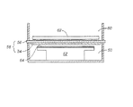
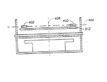
図1、図2及び図3は従来技術によるスパッタリングチャンバ50を示しており、ペデスタル52上には矩形の基板64(図1において一点鎖線で示す。)が支持されている。ターゲットアセンブリ58は、ペデスタル52に向けられた前面を有するターゲット54とターゲット裏板56とからなっており、処理チャンバの上部フランジを覆い、シールしている。ターゲットアセンブリの、ペデスタル52とは反対の側では、マグネトロンチャンバ60がマグネトロンアセンブリ62を取り囲んでいる。マグネトロンチャンバ60は真空に対して密閉されターゲットアセンブリ58(その内部には冷却液が通される)に働く差圧を抑えることができるようになっている。あるいは、マグネトロンチャンバ60には冷却液が満たされて、ターゲットアセンブリ58の裏面に接する冷却液槽を形成してもよい。矩形の基板64(チャンバ50の外形とほぼ一致している)へのスパッタリング能力を高めるため、マグネトロンアセンブリ62は両端が丸められた真っ直ぐな棒状に形成されている。マグネトロンアセンブリ62は、マグネトロンチャンバ60内を矢印68にて示すように、水平方向に前後に(往復した)パターンで移動する。マグネトロンアセンブリはマグネトロンチャンバ60内を移動して一点鎖線で示した位置62aに達する。マグネトロンの移動によってカバーされる範囲は、点線66で示される通りとなる。
【0009】
図3に示すように、マグネトロンアセンブリ62はある高さでターゲットアセンブリ58と平行に移動する。その高さは同図において誇張して示すような最低位から最高位(例えば96,98)の範囲内にある。具体的な高さ(例えば96,98)は、ターゲット54の前面から所望の距離92に従っており、これにより、使用される特定のスパッタリングプロセスやチャンバプロセス圧について望まれるスパッタリング促進の度合いが定められる。
【0010】
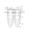
図4の断面図は、マグネトロンアセンブリに用いられた強力なネオジム−ボロン−鉄−磁石の周りにおける磁場の様子の概略を示している。例えば符号70で示される磁石の正極72,74,76,78は、永久磁石の外側ループ84(図1参照)においては上向きに(スパッタリングターゲットと反対側に)、内側ループ82(図1参照)においては下向きに(スパッタリングターゲットの側に)、それぞれ配置されるが、この極性は逆にしてもよい。磁石裏板80はマグネトロンの上側の磁場の橋渡しをしており、マグネトロンアセンブリの上側へ磁場が延びていかないようにしている。これに対して、隣合う磁石間における下側の磁場は、ループ86にて概念的に示すように、マグネトロンアセンブリ62から下側に離れるに従って弱まるものとなっている。磁力線のループ86は、磁石に隣接するループ88における比較的強い磁場を示しており、距離の増加につれて急激に磁場の強さは弱まって、磁石から最も離れたループ90では磁場の強さは相当弱くなっていることを示している。(ループは距離に応じて磁場が弱まる様子の概略である)。マグネトロンアセンブリ62が上下方向(垂直方向ともいう)に動いて、マグネトロンアセンブリ62とターゲットの表面との間の距離が増大して、距離92(図3参照)から距離94(図5参照)になると、図4で示した磁場の強さの曲線に対応するように、ペデスタル52に向い合うターゲットの前面での磁場の強さは約1/5になる。
【0011】
図6は、ターゲットとして6061アルミニウムを用いて2000kWhのパワーをかけたときのターゲットの侵食の輪郭ないしはプロファイルを示している。プロットされた等高線によれば、ターゲットの利用は概略均一であって、プロファイルラインの端部付近(滞留位置)でわずかに侵食が大きくなっている。滞留位置で見られる形状はマグネトロンアセンブリが発生する磁場の形状と対応している。ここに示したようなターゲットの侵食プロファイルは、ターゲットに向き合わせて配置された基板上の膜の厚さの均一性ないしは厚さ制御性、及び、成膜速度に関係している(ターゲットの侵食が大きくなっている領域では、基板上への成膜も大きくなる)。図6の具体例では、侵食が相対的に大きな領域が2箇所あり、ひとつは右上の隅部242で、もうひとつは左下の隅部244であり、これらに対応するようにして、スパッタされる基板上には成膜の厚さの不均一が生じる。
【0012】
今日の成膜の膜厚の均一性についての仕様は、(図6に示すような例えば50×60cmの大きな基板においても)、5%又はそれより良好であることが求められている。領域242,244に示したようなターゲットの隅部での大きな侵食の不均一は仕様を満たせるか否かに大きく影響しており、これらの部分で膜の厚さの均一性が損なわれるために、約7%の膜厚の均一性が達成されるに過ぎない。2つの領域242,244での余分な侵食を減らし、あるいは無くさなければ、膜の厚さの均一性の仕様を満たすことはできない。
【0013】
隅部における大きな侵食の観察が、その真の原因を特定できぬままに、詳細に始められた。マグネトロンアセンブリ内の複数の永久磁石の位置決めにより、マグネトロンアセンブリ全体に均一な磁場が確保される。マグネトロンが発生する磁場がほぼ均一であることは、ターゲットの表面の中央部分にわたって侵食プロファイルが均一であることから確かめられる。隅部の不均一の原因の推測は、電気的な又は磁場的な不均一が特定されるかどうかについても行われたが、何も特定されなかった。
【0014】
図7は基板の表面の膜の厚さを示すプロットである。これにより、矩形の基板の表面の膜の厚さの均一性が確かめられる。このプロットは、図6で示したターゲットの侵食とほぼ鏡像関係にあることを示している。
【0015】
薄膜の成膜分野においては、基板の大きさは、大画面LCDスクリーンの要請が高まっているので、ますます大きくなっている。例えば、現在生産されている基板サイズは400mm×500mmまでであるが、このサイズは将来的には600mm×700mmかそれ以上になることだろう。
【0016】
薄膜の成膜において最も難しい課題のひとつは、どうすれば基板全体に均一に成膜できるかである。この問題は、より大きなLCDスクリーンの経済的な生産を妨げている主要因となっている。
【0017】
上述したようなスパッタリングターゲットシステムにおける膜の厚さの均一性ないしは厚さの制御性の問題は、スパッタリングが効率的で低コストな手段として大型基板の表面コーティングに広く活用されることを妨げている。
【0018】
【発明の概要】
本発明による構成及び方法では、上述したような膜の厚さの不均一を減少させる。
【0019】
ターゲットの侵食の不均一が生じたとき、それらの箇所でターゲットにさらされている磁場の強さを変化させることで、成膜される膜の厚さの均一性ないし制御性を改善できることが見いだされた。このような箇所で膜の厚さを変化させるためのひとつの方法は、局部的には磁場の強さを変えると共に、ターゲットの残りの部分においては磁場の強さの均一性を維持することである。
【0020】
磁石部材(マグネトロンアセンブリ)はスパッタリングターゲットの近傍に配置され、磁石部材の往復動システム(駆動システム)を備えており、この駆動システムにより、磁石部材は一定のもしくは繰返しのパターンにおいて移動される。繰返しのパターンは、パターン基準面を画す一組の点列によって定められる。パターン基準面は、パターンにおける一組の水平(横方向)座標と一組の垂直(上下方向)座標によって定められる。横方向座標は、横方向位置を画成する格子を形成し、各横方向位置で、上下方向座標はパターン基準面の高さを定める。パターン基準面は、基準面上又は(基準面と平行にオフセットした)オフセット基準面上にある。
【0021】
パターン基準面は逸脱部分(相対的な移動の所定パターン)を含んでおり、この部分は、パターン基準面とスパッタリングターゲットの基準面との間の平行度についての誤差(公差)範囲から逸脱している別個の一連の高さを有している。マグネトロンが逸脱部分内で移動すると、ターゲット表面でのマグネトロンの磁場の強さが減少し又は増加する。
【0022】
スパッタリングターゲットの基準面は、その前面でよいが、これはスパッタリングターゲットの中心軸にしてもよく、又、裏面としてもよい。磁場の強さはスパッタリングチャンバに向い合うスパッタリングターゲットの表面全域において概略等しくなければならないことは、当業者にとっては自明なことであろう。従って、スパッタリングターゲットの基準面は実在の面であれ仮想的な面であれ、又この面が平面であれ曲面であれ、幾何学的ないし数学的手段によって定められたスパッタリングターゲットの表面と平行な面となる。このような平面又は曲面は連続(段差がない)であると仮定され、スパッタリングが生じる前(未使用のスパッタリング前の形状)との平行度を参照するのに用いられる。スパッタリングが開始してターゲットの侵食によってターゲットの形状が変化すると、ターゲットの侵食率が表面の各所で異なることに起因する膜厚の変化が小さくても確実に生じはじめるからである。
【0023】
基板のある部分では均一な膜の厚さとしておいて、他の部分では厚さを変えたいことがある。本発明による装置及び方法によれば、成膜する膜の厚さを磁場の強さを変化させることで制御できるようになる。概して均一な膜の厚さが得られるが、均一でない所定のパターンの膜厚を得ることもでき、例えば周縁部における厚さを増して外部へのワイヤリングを容易にすることもできる。
【0024】
ひとつの構成においては、磁場の変化は、2本のベアリングレールシステムを用いた場合、向い合うレールの相対する端部を反対方向に傾けることによって達成され得る(マグネトロンはレール上を動く移動体ないしはトラックとなっている)。これは例えば、第1のベアリングレールの一端が高く他端が低く配置され、他方のベアリングレールの低くされた端部が第1のベアリングレールの高くされた端部と向い合うようにすることで実現される。このような傾いた構成によれば、マグネトロンアセンブリの移動経路ないし表面パターン(プロファイル)は、その一部の領域において、ターゲットの基準面とマグネトロンの移動経路のパターン基準面との間の平行度の標準公差をはずれることになる。ひとつの構成においては、マグネトロンは前後の移動の一方においてはある方向に傾き、他方においては逆方向に傾く。磁場の強さはほんの少し距離が離れただけで大きく減少するので、レールの高さの変化が移動の中央部でわずか0.020〜0.030インチ(500〜750μm)でも顕著な効果が認められる。端から端まで2フィートの移動経路において、直線状レールの高さを0.030インチ変化させることで、膜厚の均一性は約8%から約3〜4%へと改善される(5%の仕様を満足することができる。)。
【0025】
本発明の別の構成においては、2本のベアリングレールを曲げ、又は特別な形にすることにより、磁石部材(マグネトロンアセンブリ又はその一端部)を特定のパターンに従ってターゲット表面に近づけたり遠ざけたりして、磁場の強さを増減させて、成膜される膜厚の均一性ないし制御性を改善することができる。
【0026】
磁石部材を横方向に(水平方向に)移動させるに際しては、幾つかの(3以上)軌道を用いてガイドすることもできる。磁石部材(マグネトロン)を2又はそれ以上のサブセクション(副構成部分)に分割することによって、ターゲットのプロファイルが均一なままに維持されるようにすることができる。例えば、略平行な3本のベアリングレール(一組の軌道)を用いて、これらの間に2個の磁石部材サブセクションを支持させるようにすることができる。外側のベアリングレールは比較的平坦で、内側のベアリングレールをたわませたり、せり上げたりして、磁場の強さを変化させる。同様に磁石部材についても、一連の磁石部材サブセクションからなる構造として(ハウジングにより連結されていても、ばらばらに分れていてもよい)、各磁石サブセクションを、処理チャンバの一端から他端に移動させる際に、それぞれのレール又は経路に従わせてもよい。
【0027】
別の構成においては、カムプレート表面は、一連のスロットと、表面フォロアとを備えている。表面フォロアは磁石部材サブセクションに連結されている。磁石部材が端から端へと移動することにより、磁石部材の各独立サブセクションの高さはカム面のパターンに追従する。また、メカニカルなカム面・フォロアシステムを用いることにより磁石の小部分の高さを変化させる以外にも、モータや上下駆動装置などの上下駆動手段を用いて、磁石部材の各サブセクションを、予め横方向位置に対応してプログラムされた輪郭に従って上下方向に移動させることによる手段も考えられる。このような移動によれば、不均一な侵食を作り出してスパッタリングの不均一が現れている箇所でのスパッタリングの強さを変化させて、このような不均一をなくし、膜の厚さの均一性を改善できる。
【0028】
スパッタリングターゲットの面とスパッタ成膜される基板との間の距離は基板に成膜される膜の厚さを決定するひとつの要素であることが知られている。しかし、大きな基板にスパッタリングする際には、ターゲットの中央はスパッタリングのパワーソースから離れているため、大きなターゲットの中央ではスパッタリングの強さが落込む傾向がある。従って、この落込みを補償するために、この箇所(領域)でマグネトロンをターゲットに近づけて磁場を徐々に強くしてもよく、膜の厚さの均一性を改善することができる。
【0029】
膜厚の均一性を改善するための他の構成は、マグネトロンの端部だけをその移動範囲の端部近傍において傾け(ロールさせ又はピッチングさせ)るというものである。マグネトロンを支持するベアリングレールは真っ直ぐで水平なままであり、マグネトロンの端部は、局部的な斜面(カム)とローラ(カムフォロア)を用いることにより傾けられる。斜面又はローラはマグネトロンの端部に配置され、斜面又はフォロアは、処理チャンバに固定された固定サポートに配置される。特定位置でのマグネトロンの横方向移動により、カムはカムフォロアに係合して、傾動力を生じさせる。傾動力はマグネトロンの端部を上下方向に押して、磁石部材の基準面を逸脱部分となるようにする。この傾動動作はローリング動作又はピッチング動作であるとすることができるが、このローリング又はピッチングなる語は、飛行機の挙動を考慮し、また、磁石(マグネトロン)を飛行機の固定翼に対応させる場合、理解されるであろう。
【0030】
マグネトロンに電磁石を用い、電磁石の磁場の強さを変化させて、膜の厚さを所望のとおりに制御することもできる。
【0031】
本発明による方法は、磁石部材をスパッタリングターゲットの近傍で横方向に移動させるステップと、前記磁石の一部分を上下方向に動かすステップとを含み、その上下方向移動距離は基準面と所定の位置での移動平面との間の平行度の誤差より大きくなっており、平面から逸脱させることで磁場の強さを変化させ、膜の厚さの制御を改善する。本発明の他の方法は、磁石部材を軌道に沿って横方向に移動させるステップと、磁石部材の一部を上下方向にも横方向に動かすのと同時に動かして、磁場の強さを変化させ、軌道に沿った1又は複数の箇所においてスパッタリングの膜の厚さの均一性を改善する。
【0032】
これらの装置及び方法によれば、従来技術では達成することのできなかった高い程度の膜の厚さの制御性を得ることができる。
【0033】
【詳細な説明】
図7及び図8の膜の厚さの均一性を示すプロットを比較することで、本発明による改善を理解することができる。図7のプロット250では、等高線のプロットはいくつかの黒くて濃い等高線を示しており、これは基板の中心から周辺の領域にわたる膜の厚さの変化を示している。非対称な(ゆがんだ)プロットは、左上の隅部と右下の隅部の成膜が大きく変化していることを示している。図7の分析による膜の厚さの均一性の変化は約8%である。これに対して、図8に示すように、本発明の装置及び方法を用いての同様なプロット260は、膜厚の均一性のプロットとなっている。この分析によるプロットは中心に対して概略対称でゆがみのない矩形となっている。中心から周辺までの厚さの変化は縦軸の両側で概略等しくなっている。図8では図7のプロットよりも最大値と最小値との間の距離が小さくなっている。この結果、膜の厚さの均一性は約4%である。
【0034】
[単一の梁型ベアリングサポート]
図9は本発明による装置の模式的な斜視図であって、この図において、マグネトロンアセンブリ272は、マグネトロンチャンバ270内を矢印274で示す方向に移動するようになっている。マグネトロンアセンブリ272は中央のベアリングサポート梁276によって支持されており、これは矢印278に示すように一様に上下動できるようになっている。一組のベアリングレール(例えば382,384)がマグネトロンアセンブリ272を、ベアリングトラック受け部材(例えば282)を介して、支持している。マグネトロンアセンブリの水平方向の移動は、ねじ付き駆動ロッド284を回転させることで行われ、この駆動ロッドは駆動ナットハウジング288に取り付けられた駆動ナット286と係合している。駆動ナットハウジングは結合ピン290a,290bに対して係合し上下に摺動可能となっており、これらのピンはマグネトロンアセンブリ272の上面に上方に向けて突設されている。結合ピン290a,290bと駆動ナットハウジング288とが摺動自在に結合されているため、マグネトロンチャンバ270の壁面に固定されたねじ付き駆動ロッド284と、サポート梁により支持されたマグネトロン272との間の上下方向の動きの差を許容することができる。摺動自在な結合によって、マグネトロンが端から端へ往復したとき、そして、図10に示すようにマグネトロンが往復した際にマグネトロンが傾斜したとき、マグネトロンの一部が上下方向に移動することが許容されている。
【0035】
図10は、図9に示したマグネトロンアセンブリの移動のようすを誇張して示した模式的斜視図である。一端から他端にかけてねじれた中央ベアリングサポートレール302に支持されたマグネトロンアセンブリ300は、横方向に移動する(この例では水平方向であるが、横方向の動きは湾曲された基板の表面(例えば球面)に沿うものでもよい)。点線304,306は、マグネトロン300がチャンバの一端から他端に横方向に移動したときのマグネトロンアセンブリの両端の高さの変化を示している(飛行機の挙動の用語を用いればロール動作である)。マグネトロンアセンブリ272,300がプロセスチャンバの一端から他端へ移動するとき、その左右の端部はそれぞれ上昇及び下降し、ターゲットアセンブリに対してそれぞれ遠くなったり近くなったりする。ターゲットの表面から離れているマグネトロンアセンブリの端部(一部分)は、スパッタリングを促進する磁場の影響を減じ、他方、ターゲットの表面に近いマグネトロンの端部は、スパッタリングを促進する磁場の影響を強める。この端部から端部へ向って傾斜する配置によれば、部材が横方向に端部から端部に動いたときに、マグネトロンとマグネトロンチャンバの両端での対向隅部におけるスパッタリングに大きな影響を与える。
【0036】
従来一般の考えによれば、マグネトロンが移動したときターゲットの全域において磁場の強さは一定でなければならない。このような考えによれば、マグネトロンの軌道とターゲットの基準面(通常は前面)との間のトラッキングの平坦度ないしは平行度についての仕様を必要とする。両部材間の平行性は、一定の磁場を提供することを意味する。1フィートあたり約5000分の1インチ若しくはそれ以下である平坦度又は平行度についての通常の誤差範囲の仕様は、請求項に記載した本発明の一態様を画す助けとなるであろう。このような誤差は、生産過程における自然な変動によるアライメントの変動を許容せず、機械的に相対する部品のアライメントも実際には制限する。本発明によるマグネトロンの端部間の高さの実際の差は、非常に微妙なものである。高さの変化が、1フィートあたり0.0075インチ程度の、平坦度又は平行度についての仕様の誤差の通常範囲から僅かに外れることで、膜の厚さの均一性に影響を及ぼすが、これは磁場の強さが距離に応じて大きく変化するためである。高さを局地的に変化させれば効果も局地的に得られる。局地的な変化は逸脱部分(平坦度又は平行度についての誤差(平行度及び平坦度の誤差はともに、通常の条件下、横方向1フィートあたりの高さ変化がプラスマイナス0.005インチ又はそれ以下、あるいは0.05%以下と定められている)を越えるマグネトロンの移動基準面の部分)として定義できる。
【0037】
従って、本発明による構成は、平坦度又は平行度についての誤差という語で定めることができる。マグネトロンが横方向及び上下方向に移動することにより形成される仮想的な面は、基準面に対する平坦度又は平行度に関して評価される。本発明による構成によれば、仮想面は、通常の平坦度及び/又は平行度の誤差範囲を越える当該仮想面の上下方向成分を有する逸脱部分を含み、この逸脱部分でのマグネトロンの移動の結果として、その移動が基板に成膜される膜の厚さの均一性が改善される。磁場の強さはマグネトロンからの距離に応じて大きく変化することから、平坦度又は平行度が次第に大きく外れるにつれて、膜厚も次第に大きく変化する。マグネトロンの軌道の端部において平坦度又は平行度から0.030インチ外れることで、若しくはマグネトロンの端部において約10mm平面から外れることで、図9の構成において、基板及びターゲットの相対する隅部における膜の厚さの均一性を変動させるが、これは、図7のプロットに比較して明らかに改善される(図7の設定においては平坦度又は平行度の誤差はレールの端から端にわたって、最大で0.010インチの通常範囲に納っている)。高さを変化させることで、図8に示すように、膜の厚さの均一性は5%の仕様の要求を満たすように改善される。
【0038】
この例は本発明のひとつの実施形態にすぎず、同様の技術を用いて膜の厚さの均一性又は制御性が必要な箇所での改善を図ることができる。マグネトロンの動きを調整して、マグネトロンの移動を表す仮想面パターンに、通常の平坦度又は平行度の誤差範囲を越え且つスパッタリングされるターゲット表面での磁場を変化させる逸脱部分を含めるようにすることで、基板に成膜される膜の厚さの均一性や制御性を改善することができる。
【0039】
一端から他端へ、片側から反対側へと移動したときに、平坦度及び平行度についての仕様を越えた部分の上下方向の変化は、マグネトロンアセンブリ272の移動によって生じた仮想的な基準面パターンないしはプロファイルに重ね合わされた仮想的な基準面と対比して、計測される。マグネトロンアセンブリ272が平坦度又は平行度を離れる動きの特性を示す立面図が、直線的なマグネトロンアセンブリ272の傾動については図11、図12及び図13に示されており、マグネトロンアセンブリの曲がりについては図21、図22及び図30に示されている。両形態においても、マグネトロンアセンブリ272の移動の端部の近傍における当該マグネトロンアセンブリ272の端部は、いずれの実施形態においてもマグネトロンアセンブリ272の端部はその移動の端部付近において通常の(さもなければ選定された)誤差(例えば0.005インチ/フィート,0.0075インチ/フィート,0.010インチ/フィート,0.015インチ/フィート,0.020インチ/フィートインチ/フィート,0.025インチ/フィート,0.030インチ/フィート,0.035インチ/フィート,0.040インチ/フィート,0.050インチ/フィート(マグネトロンの端部において約10mmの高さ変化を生じさせる))を越えるよう上昇され、スパッタリング成膜される基板表面全域にわたる膜厚の均一性又は膜厚の制御性を改善するようになっている。
【0040】
図11、図12及び図13は、図9に示したマグネトロンチャンバ270の一端から他端にマグネトロンアセンブリ272が移動したときのその挙動(傾き又は曲り・ロール)を順次示す断面図である。中央サポートレール276は図9及び図15に示した一体型(one−piece)のベアリングフレーム380を支持している。概略的に言えば、ベアリングレール382,384は互いに平行になるように固定されるよう構成されている。しかし、図16に示すように、ベアリングレールの一部について、図示された穴の間においてその上面に切込み392を設けると共に、そのプロセスに応じて通常は厚さ0.010インチの倍数で0.060インチまでの、例えば0.050インチのシム、例えば符号394,396のものを、一体型のベアリングフレーム380と中央ベアリングサポート梁276との間であって、その両端で、相対する側にて、適所に配置し固定するならば、シムはベアリングレール382及び384にわずかな高さ方向の曲げを生じさせる。中央ベアリングサポートにおけるわずかな高さ方向のずれ(オフセット)371(図13)は、マグネトロンがその端部に向かって外方に行くにつれて拡大され、その端部では、高さ方向のずれが最大値(約10mm)となる。ベアリングレール382,384の構成により、マグネトロンアセンブリ272は当該レールの経路に従う。マグネトロンが移動すると、その動きにより、マグネトロンアセンブリ272の各点をトレースした仮想面パターン(飛行軌跡)内の一連の点列が形成されている。仮想面パターンにおけるいくつかの点は、基準面との平坦度又は平行度の誤差よりも大きな距離で、仮想的な水平面に対して上下方向にオフセットしている(仮想的な水平面とは、仮にベアリングレールが横移動の中立軸368(図12参照)から上下方向にオフセットされておらず、水平な基準面のパターンと交差していないとした場合、マグネトロンアセンブリが移動するであろう面である)。ベアリングレールの高さ方向の位置調整は、シム394,396に代えて、又はこれらと共に、一体型のベアリングフレームの側面に締め付けられるボルトが通る垂直なスロットを用いることにより、なされ得る。
【0041】
図13に示すように、ベアリングレールフレーム360に上下方向に切れ目を入れて、左側を上下方向に距離370だけオフセットさせることで、マグネトロンアセンブリは一点鎖線372に示すようなロール動作を行うことになる。中心軸364からのベアリングレールのオフセットは距離366にセットされている。図11においては同様にベアリングレール362を分割している右側部分が、中心軸368に対して距離371(約10mm)だけオフセットしており、マグネトロンは一点鎖線374に示すようなロール動作を行うよう、示されている。このように、中央サポートにおけるわずかな高さの変化は、中央サポートレール276を越えて延びるマグネトロンアセンブリ272の最端部において大きな高さの変化を生じさせる。
【0042】
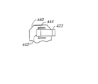
図17〜図20、図17A、図18A、図20A及び図21〜図24は、本発明により中央サポート梁276に支持されたマグネトロンの別の構成を示している。この構成においては、ベアリングレールを傾けるのではなく、ベアリングレールは本来の平坦で水平な姿勢に維持される。この姿勢は、干渉がなければ、ターゲットアセンブリの基準面に対してマグネトロンの平坦な平面上の移動軌跡を与えるものである。この構成においては、マグネトロンアセンブリ272は中央ベアリングサポート梁276のみによって支持されるわけではなく、マグネトロンアセンブリがチャンバの端部に近づいたときにはカムフォロア(ローラ)442が斜面(カム)422に係合して、マグネトロンアセンブリの端部が、スパッタリングターゲットアセンブリの上方に向けて屈曲され又は傾けられるようになっている。斜面422,428はチャンバの相対する隅部(スパッタリングターゲットの過度の侵食の変則性が観察される位置に対応する部分(図6))に配置されている。この構成では、剛性があり実質的に変形しないマグネトロンハウジングを、中央ベアリングレールのベアリングトラックに対してマグネトロンを保持するために、スプリング負荷式のジョイントと共に用いることができる。スプリングは、マグネトロンがベアリングレールに対して真っ直ぐで水平に保持されるように、負荷が加えられると共に、マグネトロンの端部がカムと接触して持上げられる状態になったときに、中央ベアリングレールを枢軸として傾動することができるよう、負荷が加えられている。他の構成では、マグネトロンハウジングを容易に変形できるプラスチックやゴム又はそれに類する材料で作っておき、中央ベアリングトラックに対して中央レールに剛的な結合を与え、マグネトロンの端部がカム(例えば422)に接触した状態では、マグネトロンが曲線状に湾曲し、その端部がターゲットアセンブリから持ち上げられるようにしている。このときのロール動作ないしはロール姿勢は図21と図21A、及び、図23と図23Aを比較されたい。
【0043】
図17、図17A、図18、図18A、図19、図20及び図20Aは、一連の関連ある断面図であって、マグネトロンアセンブリ272の端部の動きを示しており、所定位置に配置されたカム(斜面)及びカムフォロア(ローラ)により、マグネトロン全体又はマグネトロンの一部がターゲットアセンブリに近づいたり離れたりする様子を示している。図17に示されるように、マグネトロンアセンブリはカムフォロア(ローラ)442とカム面(斜面)422を用いることで寸法432に示されるような上下のロール動作を行う。マグネトロンアセンブリ272の端部440には、持上げローラ442を備えた持上げローラフレーム444が備えられている。持上げローラ442とフレーム444はマグネトロンアセンブリ272の端部(片端440のみを示している)と共に移動して、持上げローラ442が、サポート固定具(例えばサポートブロック446)によりチャンバに固定された持上げ斜面422に係合したときに、斜面422を転がり上がって上昇し、それにつれてマグネトロンアセンブリの端部は距離432だけ反り上がる。この構成においては、斜面422,428に係合したときには、マグネトロンアセンブリ272を端から端へと移動させようとする力は、マグネトロンの端部(例えば440)をそりあげさせる力にもなる。図21、図22及び図23における一点鎖線424,420,430は、マグネトロン272が端から端へと移動したときの、理想的な曲げ、直線、曲げ挙動(形状)をそれぞれ示している。理想的な状態においては、マグネトロンアセンブリ272の一側はターゲットアセンブリの基準面に対して真っ直ぐで平行な状態で、他側だけが図示のように概ね屈曲して反り上がっているが(水平な一点鎖線の直線はマグネトロンアセンブリの端部の高さ変化を評価するための基準である)、実際には、トラックにおける直線状のベアリングとベアリングレールとの間にやや遊びがあり、自由端でも上下方向の動作が生じるので、アセンブリの自由端においてもある程度の影響が生じる。
【0044】
図24の平面図においては、左上の隅部の斜面422と右下の隅部の斜面428が示されている(この部分においてマグネトロンアセンブリは、例えばゴムのような容易に変形できる材料でできている場合、過度の応力を生ずることなく弾性的に曲る)。マグネトロンアセンブリ270が図24の22−22線で示された中央の水平姿勢(形状)420から、21−21線で示された姿勢のチャンバの第1端に移動したときに、マグネトロンアセンブリの曲る様子は一点鎖線424にて示されており、マグネトロンアセンブリの端部は中心線(例えば420)から寸法426だけオフセットする。同様にして、23−23線に示されるチャンバの他端部にマグネトロンアセンブリ272が移動したときには、マグネトロンアセンブリの屈曲の姿勢は一点鎖線430で示され、中心線(例えば420)から寸法432だけオフセットすることになる。対称的なシステムにおいては、マグネトロンアセンブリの両端部が曲ることによる上下方向のオフセット寸法432,426はほぼ等しい値にすべきであるが、経験的なデータから、種々のオフセットが必要であることがわかっている場合、各端部における上下方向のオフセット寸法を異なるようにすることもできる。また所定のパターンでの均一ではない膜の厚さをスパッタリング制御することも可能である。
【0045】
図17A、図18A及び図20Aは、4つの斜面(又はカム)415,416,417,418を用いた例を示しており、これは、中央ベアリングレールトラックに対するスプリング負荷式の中央マグネトロン結合部(図示せず)を有している。マグネトロンの端部の平面図は図17Aに示されており、マグネトロン272aの側面の側方に2組のローラ434,436が配置されている。マグネトロンがその横方向動作の端部に近づくと、片側に2つずつ設けられたローラ(ここでは一方のみを例えば434として示している)が2つの斜面(すなわち415,418)に接触し、マグネトロンは上方へのピッチ(揺れ)を受け、チャンバの縁部に最も近いマグネトロンの縁部が距離432aだけ持ち上げられる。マグネトロンのピッチ(再び飛行機の挙動について参照されたい)の変動によるこのような縁部の持上りにより、ターゲットアセンブリの縁部における磁場の強さは減少し、このようにしなければエッヂ効果で発生するであろう余分な成膜が避けられる。このように、マグネトロンはロール及びピッチの挙動変化を受けるようになっている。ヨーイング挙動の変化についても、ベアリングの軌道を直線形状にしないようにした場合、又は、マグネトロンの隣合うベアリングトラック間の差動を許容するサスペンションをベアリングトラックに設けた場合には、可能となる。
【0046】
上記において概念的に説明したマグネトロンアセンブリの構成は、実際のメカニズムとしては、図25及び図26に示すようになる。
【0047】
図25及び26はマグネトロンアセンブリ118の底面図及び断面図であり、マグネトロンアセンブリ118は、直線状ベアリングサポート部142と水平延長部144とからなる中央ベアリングサポートフレーム136によって支持されている。直線状ベアリングサポート部142は、その両側のベアリングレール138,140(一組の軌道)に固定されている。マグネトロンアセンブリ118は、一組の直線状レールトラック120,121を介してベアリングレール138,140によって支持されている。直線状レールトラックはマグネトロンアセンブリ118に固定されており、直線状リニアレール138,140上を前後に摺動する。マグネトロンアセンブリの前後方向(水平ないしは横方向)への移動は、ねじ駆動ロッド(ボールねじ)112の回転によって行われ、ボールねじはボールねじ受け用ナット122に螺入され、ナットには一組のナットハウジングピン受け用穴126,128が備えられている。一組の駆動ピンがマグネトロンアセンブリ118から上下方向に延び、穴126,128内に上下方向に摺動自在に挿入され、直線状レール138,140と回転可能なねじ駆動ロッド112との間の不整列による機構の拘束を防止するようになっている。ねじ駆動ロッドは、チャンバ上部外側で支持されたボールねじ駆動モータ114によって回転され、ボールねじの第2端部はボールねじ端部ベアリング116によって支持されている。この構成では、中央ベアリングサポートフレーム136の上下方向の移動は、垂直に配置された一組のリードねじ148,150,152を回転させることで達成され、これらには、歯付き駆動ベルトプーリが取り付けられている。駆動プーリ・モータ156は、歯付き駆動ベルト154によって歯付ベルトプーリに連結されている。ベルト駆動プーリ・モータ156が回転すると、これと同時にプーリ148,150,152が回転し、固定されたナットに螺合しているピッチの等しいリードねじが回転し、中央ベアリングサポートフレーム136を昇降させ、このとき直線状ベアリングサポート部142とターゲットとの平行度は維持されるようになっている。
【0048】
伝統的な構成では、マグネトロンアセンブリ118の水平挙動は、きわめて精密に整列配置されたベアリングレール138,140に対する摺動取付具により制御される。
【0049】
この態様では、マグネトロンアセンブリの動きは、ターゲットが侵食され又は用いられる前のスパッタリングされていないほぼ平坦な前面形状に対しては平行で均一となる。この構成は、サイズが最大約400mm×500mmまでの比較的小さな矩形基板のスパッタリングに用いられる。
【0050】
本発明による構成を用いてマグネトロンを傾動すべき場合には、ベアリングレール138,140を傾動する(例えば図22の構成により示されるように)と共に、中央ベアリングサポートフレーム136を、ターゲットアセンブリに対して平行な状態を保ったままで昇降させるようにする。
【0051】
本発明による方法においては、図25及び図26に示すようなマグネトロンアセンブリがターゲットアセンブリに沿って横方向に移動したときに、マグネトロンアセンブリを上下方向に移動させる。しかしながら、図6に示したようなターゲットの深さ方向の侵食プロファイル(形状)の変化が与えられたときには、マグネトロンアセンブリを平行に上下させることによっては、現在の垂直に固定された構成と比較しても、膜厚の均一性や膜厚の制御性の改善を行うことはできない。他の構成としては、それぞれの上下方向サポートを個々独立のモータ又はアクチュータによって駆動して、サポート梁とマグネトロンアセンブリの上下方向の移動の制御をマグネトロンアセンブリの横方向の位置と関連づけて電気的に制御することも可能である。
【0052】
[2本の平行な梁型ベアリングサポート]
約600mm×700mmのサイズのより大きな矩形基板に対しては、図27及び図28に概要を示し、図34及び図35に詳細を示した第2の機構を用いる。
【0053】
図27は本発明による第2の機構の概略を示している。マグネトロンチャンバ310には、マグネトロンアセンブリ312が設けられている。マグネトロンアセンブリ312は2本のベアリングサポート梁316,317によって支持されており、これらは、一組のベアリングトラック(例えば324)に固定されたマグネトロンアセンブリ312が、一組のベアリングレール(例えば322)に沿って矢印314に示すように横方向に移動できるようにしている。ベアリングサポート梁316及び318の上下方向の移動は、矢印320によって示されている。マグネトロンアセンブリ312をベアリングレール322に沿って横方向に移動させるにはねじ駆動ロッド326の回転によって行う。このロッド326は、駆動ナットハウジング330内に収容された駆動ナット328と係合している。駆動ナットハウジング330は、可撓性のあるスプリング状の結合部材332の弓状部分に固定されている。この結合部材332はマグネトロンアセンブリ312に固定され、ベアリングサポート梁316,317と駆動ナット326との間の不整列ないしは相対的な動きが上下方向において柔軟な結合性を与え、一方、横方向においては剛性を与えるようにしている。図28は、図27の構成におけるマグネトロンアセンブリ312の理想的なトラッキング(軌道)を示している。図28において、マグネトロンアセンブリ342は2本のベアリングサポート梁344,346に支持されており、これらの梁は端部フレーム348,350により支持されている。この構成では端部フレーム348,350は互いに平行で水平になっている。左側のレール344の位置状態は、マグネトロン342の左側端部がフレーム348の下縁部からその反対側のフレーム350の上縁部へと、上下方向に変化していることを示している。また、右側のベアリングサポート346の位置状態は、端部フレーム348の上縁部からその反対側の端部フレーム350の下縁部へと、上下方向に変化していることを示している。
【0054】
端部レールにより支持されたマグネトロンは、図29〜図33に図示されている。図29はマグネトロンアセンブリ312を含むプロセスチャンバの断面図を示しており、このマグネトロンアセンブリ312は2本の支持レール400,402によって支持されている。この構成は図27及び図28の概念的に図示したものに対応している。図30(図33の30−30線の位置に対応する)に示される一方の最端部において、レール402の端部における上下方向のオフセット量は、距離408aとして示され、マグネトロンアセンブリの挙動(傾き)は、ほぼ一点鎖線412で示した通りとなる。図31(図33の31−31線の位置に対応する)に示された中央の位置においては、水平の姿勢404は、マグネトロンがターゲット表面又はターゲットの基準面(通常は平面)に対して平行になるようにしている。図33の32−32線に沿っての断面図である図32に示されるプロセスチャンバの第2端部では、ベアリングレール400はターゲットアセンブリの基準面(例えば、図31の404と平行な面)より上方に位置し、これにより、マグネトロンアセンブリ312を一点鎖線414で概ね示したように挙動(傾け)させる。上下方向のオフセット距離は408bとして示されている。この例においては、処理チャンバの横に延びる中心線406からの水平方向オフセットは距離410であり、そのために梁での上下方向のオフセット寸法408a,408bを大きくしなければ、図11〜図16に示した形態のマグネトロンアセンブリと比較して同様な挙動(傾き)変化を生じさせることはできない。図11〜図16の場合では、相対する支持レールの近傍に配置されたベアリングレールにおける小さな上下方向のオフセットが、マグネトロンアセンブリ312の一端から他端にかけて、単位長さあたりの同様な挙動変化(傾き)を生じさせる。
【0055】
図34及び35の詳細図は、スパッタリングチャンバと共にあるべきマグネトロンチャンバにおいて使用されるマグネトロンアセンブリ178を示している。マグネトロンアセンブリ178(図34においてはマグネトロンアセンブリの一の位置と別の位置が示されている)は、一組のベアリングレール206,208上に支持されており、これらのレールは一組の擬似的な平行縁部ベアリングサポート198,200上に支持されている。一組の直線状レールトラック180,182がベアリングレール206,208と係合しており、ねじ駆動ロッド(ボールねじ)172(図34においては一点鎖線のみで示している)を駆動することで前後に移動される。この機構において、マグネトロンアセンブリ178の前後の動きは駆動ロッド172の回転によってなされ、駆動ロッド172はボールねじ駆動モータ174とボールねじ端部ベアリング176との間に取り付けられている。ボールねじ172は、ボールねじナット受けハウジング186に取り付けられたボールねじ受けナット184と係合している。ボールねじ受けハウジング186は、可撓性のある板ばね状の結合部材188に固定されており、この結合部材188はマグネトロンアセンブリ178の端部付近にてマグネトロンアセンブリ178に結合されている。上述の機構と同様に、ベアリングレール206,208は、互いに平行に且つスパッタされるターゲットの面に対しても平行となるように正確に配置されており、基板への均一な成膜が行われるようにしている。
【0056】
図34及び図35のマグネトロンアセンブリはベアリングサポート198,200に支持されており、これらのサポートは端部サポートフレーム部材202,204と共にフレームとして機能するよう互いに整列されている。上下方向の調整を可能とするために、フレーム上のねじ受けナットと係合される4本のねじ付サポートロッド(ベアリングに取り付けられている)が、歯付きプーリ210,212,214及び216に固定されている。歯付き駆動ベルト222は歯付きプーリ210,212,214及び216と共にアイドラプーリ218,220を一周するように掛け渡され、駆動プーリ及びモータ224によって駆動される。ベルト駆動プーリ及びモータ224が回転すると、四隅に配置されたリードねじの各々が、それぞれに取り付けられた歯付きプーリを介して回転させられ、ベアリングサポートフレームが水平状態を保ったまま、上下方向に調整される。他の構成としては、各上下方向のサポートを別々のモータ又はアクチュータによって駆動し、サポート梁とマグネトロンアセンブリの上下方向の動作の制御をマグネトロンアセンブリの横方向の位置に関連づけられた電気的な制御により行うようにしてもよい。
【0057】
[2ピース・ヒンジ結合型のマグネトロン]
図36及び図37には、他の構成によりマグネトロンアセンブリ460及びその上下方向の動作についての他の形態が示されている。これらの図においては、中央サポートレール462を用いてヒンジ式ないしは蝶番式に結合されたマグネトロンアセンブリ460の断面を示しており、中央サポートレール462は、図37に示されるように連続的に湾曲され得るもの、或は、一連の直線状セグメントからなるものとすることができる。これらの構成において、マグネトロンアセンブリ460のヒンジ結合された2つのセクションの中央交差部分は、中央ベアリングレール462から支持されており、マグネトロンアセンブリが一端から他端にサイクル運動したときにマグネトロンアセンブリ460の中央部とスパッタリングターゲットとの間の距離を変化させることができる。ヒンジ式に結合されたマグネトロンと真っ直ぐなマグネトロンとを比較した場合の水平方向の寸法差による水平方向の距離の変化は、周辺のベアリング梁を内側に湾曲させることにより、又は、中央サポートレール462に取り付けられたベアリングトラック間を固定的に結合することにより(しかし、側部サポートレール464,466に対するベアリングトラックの結合は、自由に、中央ベアリングレール462に対して接近又は後退運動(摺動)を可能とする)、許容され得る。なお、このような結合部の詳細構造は、当業者によって作り実施され得る。
【0058】
[基準プロファイルに追従する分割型マグネトロン]
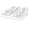
図38は、本発明による他の実施形態を示している。この実施形態においては、1又は複数のカム面とカムフォロアが用いられ、それぞれ独立に移動できるマグネトロン・サブセクションを有するマグネトロンアセンブリの部分間での距離を変化させると共に、マグネトロンの磁石列における隣合う永久磁石同士が連続したループを描く外形を維持するようにしている。磁石サブセクション(一連の磁石部材サブセクション)は、枢動自在とすることができ、連続した磁場を提供すべく鎖のように互いにヒンジ結合されることができ、或は、可撓性のあるハウジング内に収容されることができる。図38に示すように、いくつかのカム面(一連のカム面)は、マグネトロンの各サブセクション、ひいてはマグネトロンアセンブリが全体として追従するプロファイル(profile)/パターンを反映する連続したカム面板476を形成すべく、互いに組み合わされ得る。カム面板476にはいくつかのカム面スロット(例えば478)が備えられており、これを通ってカムフォロアロッド(例えば474)が、カムフォロア(例えば482)とマグネトロンアセンブリのサブセクション(例えば472)とを結合している。マグネトロン輪郭(contour)トラッキングフレーム486は、カムフォロア(例えば482)とマグネトロン・サブセクション(例えば472)との間の上下方向の整列状態を維持し、これらが一体的にトラッキング(水平方向の駆動手段によって駆動された場合)することで、膜の厚さの制御性及び/又は膜の厚さの均一性を改善するようにしている。プロファイル面パターンの各トラッキング(追随)によって、マグネトロンアセンブリの特定のサブセクション(例えば472)の各々とその下のターゲットとの間の距離が変化する。
【0059】
図38Aは本発明による他の構成を示している。図38Aにおいては、マグネトロン488は可撓性のある材料でできており、各上下方向の制御部材(一連の上下駆動部材の制御部材)がマグネトロン488の各部分の垂直上下動を制御するようになっている。トラッキングフレーム486はわかりやすくするために、破断して示している。この構成においては、上下方向制御部材(プッシュ/プルロッド)の数を増加させることにより、及び/又は、マグネトロンの各側にこのような上下方向制御部材を設けて必要なピッチ挙動が得られるようにすることにより、マグネトロン488のターゲットに対する影響を精密に制御することが可能である。
【0060】
図39〜図42は、カム面476に利用可能ないろいろな面パターン/プロファイルのうち三種類を理想化された概念図として示したものである。
【0061】
図39における面パターン/プロファイルは、図9〜図15に示した構成のマグネトロンアセンブリによりトラッキングされた面パターン/プロファイルと同様になっている(相対する隅部が高く、他の相対する隅部が低くなっている)。このプロファイルにおいては、後方の隅部494と前方の隅部498が低くされ、一方、右側の隅部492と左側の隅部496が持上げられている。従って、右の隅部492に低い隅部498を表面上連結しているレール間の高さの変化は、低から高へと変化し、一方、後側の隅部494から左の隅部496に連結しているレールは高から低へとなっている。
【0062】
図40には、2次元の円形状の若しくはパラボラ型の曲面を示している。湾曲面ないしは円弧形状の面の高位点は水平な中心軸503に沿って配置されている。実際にはベアリングレールの高さは図示の曲面の縁に沿って追従し、例えば右隅部504から下隅部510にかけて、又は上隅部506から左隅部508へと追従している。
【0063】
図41に示した面プロファイル/パターンの輪郭は、上方に開いたパラボラ型ないし円形型を示しており、これにおいてはすべての隅部、すなわち右隅516、後ろの隅部518、左隅部520及び前方の隅部522が略等しい高さに持上げられており、中央部515は低い位置になっている。この面パターンに従うマグネトロンアセンブリは、マグネトロンアセンブリの磁石列の各磁石サブセクションを有しており、これらのサブセクションによって、磁石列の中央部分はターゲットの裏面に近づいて、その場所におけるスパッタリングを増強させる。或はまた、この構成は、磁場の影響が円形もしくはパラボラ型のターゲットを均一にスパッタリングして、特別な形状のマグネトロンを形成する必要なく、同様な円形やパラボラ型の基板(例えばパラボラ型反射鏡)にスパッタリング成膜するよう、用いられることもできる。この構成を用いた場合、図41に示したようなマグネトロン・サブセクション用の面パターン/プロファイルを用いることで、成膜される膜の厚さを比較的一定に保つことができる。
【0064】
図42には凹形の下向きの円形ないしパラボラ型を示しており、4つの隅部528,530,532,及び534はこのプロファイル/パターン面の低位置になっており、中央の527の点がプロファイル/パターン面の高い点となっている。
【0065】
当業者は理解するであろうが、機械的なカム形状(例えば図38)又はその他の全体に適度に連続的なカム面プロファイル/パターンを用いて、マグネトロン・サブセクションとターゲットアセンブリとの間の距離を変化させることができる。しかし、図に示した面パターン/プロファイルは、多くの面パターンのバリエーションのうちの利用可能ないくつかのものに過ぎない。カム面/プロファイルの変化は、特定の場所においてスパッタリングを局所的に変化させたい場合にそれに応じてカム面を変形することで適用することができる。
【0066】
[上下アクチュータ]
本発明による装置の他の構成では、図43に示すように、略平板からなる平坦なフォロア板546と、マグネトロンの各サブセクション(例えば542)の横方向位置と上下方向位置とを関連づける構造とを用いている。各サブセクション(例えば542)は縦棒(例えば544)を介して輪郭プレートフォロアアクチベータ(例えば552)に結合されている。これらによってアクチベータアセンブリ(例えば550)ができている。アクチベータアセンブリ(例えば550)は、平坦なフォロア板546のスロット(例えば548)内をマグネトロン輪郭トラッキングフレーム558(一点鎖線にて示す)の動きに従って移動する。マグネトロントラッキングフレームによって全てのアクチベータアセンブリが結合され、マグネトロンアセンブリ(全てのマグネトロン・サブセクションを含む)がターゲットアセンブリに沿って横方向に掃引動作(scanning)した場合に、これらが横方向に同時に動くようになっている。各マグネトロン・サブセクション542の上下方向位置は制御システム554により設定され、制御システムは、マグネトロンが端から端へと移動したときの各マグネトロン・サブセクションについての高さを定める高さ制御データを受け取るようになっている。高さ制御データにより、磁石サブセクションは、プログラムされた面プロファイル/パターンによるプログラムさせた態様で移動される。電気的プログラミング(輪郭ジェネレータ556のプログラムに従ってアクチベータがマグネトロン・サブセクションを移動させるプログラム)を用いて、プログラムされたパターンは磁石の小部分をあたかもメカニカルなカム面(例えば図38に示したような)に従うようにして移動させる。なお、輪郭ジェネレータは、制御システム554に基準輪郭ないしは基準等高線を提供するものである。輪郭データのプログラミングは簡単に変更することができ、所望の面パターン/プロファイルに応じたマグネトロンのトラッキングを調整できる。
【0067】
[スパッタリングの電磁石式マグネトロン制御]
図44及び図45は、スパッタリングを制御するために用いられ得る電磁石を用いたマグネトロンの構成を示している。マグネトロン560はターゲットの表面とほぼ平行な面内で保持されており、ターゲットアセンブリの裏面に沿って前後に掃引動作するようになっている。マグネトロン560が移動されると、マグネトロン内の電磁石は付勢され、列をなす各電磁石のそれぞれが発生させる磁場の強さが輪郭プロット556aに従って変化される。このプロット556aは、物理的形状の変化についての経験的な知識にもとづいた所望の成膜プロファイルを示したものである。従って、マグネトロンが前後に移動したとき、磁場は電気的に変化させられ、永久磁石によるマグネトロンをターゲットアセンブリの裏面に近づけたり遠ざけたりしたときと同様な結果が得られる。このような構成における磁石列には、永久磁石と電磁石を組み合わせてたものを含ませるようにしてもよく、また、このような電磁石を高さ方向の移動に関連して、あるいは、水平方向の移動に関連して用いてもよい。極端な例においては、電磁石の列を、基板表面全体をカバーするエリアを有するように固定して、磁場の強さの変化を、選択された電磁石への通電及び断電を制御することで電気的に制御するようにしてもよい。
【0068】
図45は、マグネトロン560に電磁石を用いた構成を示している。磁石は図4におけるのと同様に配列されており、違うのは各永久磁石セグメントの代りに電磁石コア(好ましくは鉄)(可能ならば図示のようにスプール564の形状のコア)を配置している。なお、各スプールにはワイヤ巻線が巻き付けられている。磁場の強さは輪郭コントローラ554aに接続された配線576によって独立に制御される。マグネトロンが前後に移動したとき、磁場の強さは電磁石のコイルに供給される電流の大きさを可変することで変化させられ、スパッタリングもこれに従って促進される。
【0069】
本発明における方法であって、スパッタリング中に基板に成膜される膜の厚さを選択的に制御するものにおいては、スパッタリングターゲットの近傍で磁石部材を横方向に移動させるステップと、磁石部材が水平方向に動いたときに磁場の強さを変化させてターゲット表面でのスパッタリングを促進させ、スパッタリング中に処理中の基板上に特定の膜厚のパターンを成膜するステップとを含んでいる。膜厚を均一にするよりも違えることが望ましい場合もある。例えば、基板に成膜された導電層とのワイヤリング結線の耐久性を増し、割れが生じにくくするために、基板の縁部での膜の厚さを増加させることが望まれる場合もある。一般的には、局部的な膜の厚さの不均一が望まれるかどうかにかかわらず、基板のほぼ全体にわたる膜厚の均一性についての誤差(公差)が維持されなければならないことが望まれる。本発明による構成及び方法によれば、膜の厚さが均一であることが望まれる箇所では均一に、不均一であることが望まれる箇所では不均一にすることができる。
【0070】
本発明の方法によれば、マグネトロンアセンブリ又は磁石セクションを横方向に動かすと共に、垂直サポートによりマグネトロンアセンブリの少なくとも一部をその水平方向の位置に応じて高さ方向に移動させて、膜の厚さの均一性を改善する。
【0071】
本発明による方法においては、磁石部材をスパッタリングターゲットの近傍で横方向に移動させるステップと、前記磁石の一部を上下方向に移動させるステップとを含み、その距離を基準面と所定の位置での移動平面との間の平行度の誤差(公差)範囲より大きくすることで、平面から逸脱する磁場の強さを変化させて、膜の厚さの制御を改善する。本発明の他の方法では、磁石部材を軌道に沿って横方向に移動させるステップと、磁石部材の一部を横方向に移動させると同時に上下方向にも移動させて、軌道に沿った1つ以上の箇所におけるスパッタリングに対して用いられる磁場の強さを変化させて、スパッタリングに関する膜の厚さの均一性又は制御性を改善するステップとを含んでいる。磁石部材は軌道に沿って横方向に移動され、且つ、磁石部材の横方向の動きと同時に磁石部材の一部は上下方向に移動させられ、軌道に沿った1又は複数の箇所におけるスパッタリングに対して用いられる磁場の強さを変化させ、スパッタリング中に成膜される膜の厚さの制御性を改善することができる。
【0072】
本発明による方法では、磁場の強さを変化させるステップは、磁石部材の横方向の位置に応じたパターンに従って磁石部材の電磁石の強さを変化させることを含んでいる。
【0073】
本発明は上述のように具体的な実施形態に基づいて説明したが、当業者ならば本発明の範囲及び精神から逸脱することなくその形態や詳細部分を変更することができることを理解するであろう。
【図面の簡単な説明】
【図1】従来技術によるマグネトロン装置の模式的な平面図である。
【図2】図1の従来技術によるマグネトロンチャンバから、ターゲットアセンブリによって隔てられたスパッタリングチャンバを示す断面図である。
【図3】図2の装置の側面断面図であって、マグネトロンの磁場がスパッタリングターゲットを越えて延びているようすを概念的に示している図である。
【図4】永久磁石を含むマグネトロンと、そこから下向きに磁場が発生している様子を概念的に示した断面図である。
【図5】図2の装置についての第2の側面断面図であって、マグネトロンを最上位の位置に持上げたときにマグネトロンの磁場がかろうじてスパッタリングターゲットを越えるようすを概念的に示している図である。
【図6】従来技術によるターゲットの浸食プロファイルであって、スパッタリングの最中のスパッタリングターゲットの浸食(利用)のパターンを示している図である。
【図7】従来技術によるマグネトロンチャンバを用いたスパッタリングターゲットについての基板上の膜厚プロファイルを示すもので、5点式プローブを用いて測定したシート抵抗値(膜の厚さと逆比例する)分析により得られたプロファイルを示す図である。
【図8】本発明の構成及び方法を用いた場合におけるスパッタリングターゲットアセンブリの膜厚の等高線プロットであって、5点式プローブを用いて測定したシート抵抗値(膜の厚さと逆比例する)分析からの等高線プロットを示す図である。
【図9】マグネトロンを支持するために中央ベアリングレールを用いているマグネトロンチャンバを示す模式的な斜視図である。
【図10】図9の中央マグネトロンサポート梁を寸法的に誇張して示す模式図であって、当該サポート梁が中央梁サポートに沿って移動した場合にサポート梁がねじれる様子を示す図である。
【図11】図14のマグネトロンサポート梁の11−11線における断面図である。
【図12】図14のマグネトロンサポート梁の12−12線における断面図である。
【図13】図14のマグネトロンサポート梁の13−13線における断面図である。
【図14】中央マグネトロンサポート梁を備えている本発明によるマグネトロンチャンバの平面図である。
【図15】例えば図9に示すような中央梁に支持されたベアリング軌道(レール)を備えたベアリングチャンネル梁を示す斜視図である。
【図16】ベアリング支持レールを改良したものを示す図であって、チャンネルが分割され、チャンネルの両端の片方が持上げられて、マグネトロンの一部分を上下方向に移動させるようにしているものを示す図である。
【図17】図18に示すマグネトロンの端部を示す平面図であって、斜面(カム)に係合して持上げられようとしている状態を示す図である。
【図17A】図18Aに示すマグネトロンの端部を示す平面図であって、斜面(カム)に係合して持上げられようとしている状態を示す図である。
【図18】図20及び図24中の18−18線におけるマグネトロンチャンバの部分断面図であって、チャンバの端部において斜面によってマグネトロンの端部が持上げられるようすを示す図である。
【図18A】図20A中の18A−18A線におけるマグネトロンチャンバの部分断面図であって、チャンバの端部において斜面によってマグネトロンの端部が引っ掛けられるようすを示している図である。
【図19】マグネトロンと斜面との位置関係を示す断面側面図である。
【図20】マグネトロンチャンバの平面図であって、相対する隅部の斜面によってマグネトロンの端部が持上げられるようになっているものを示す図である。
【図20A】マグネトロンチャンバの平面図であって、各隅部の斜面によってマグネトロンの端部が持上げられるようになっているものを示す図である。
【図21】図24中の21−21線における模式的な断面図であって、変形可能な水平なマグネトロンの端部がそり上げられて曲線形状になったようすを示している図である。
【図21A】図24中の21−21線における模式的な断面図であって、剛的な水平なマグネトロンの端部が持上げられたようすを示す図である。
【図22】図24中の22−22線における模式的な断面図であって、変形可能な水平なマグネトロンを示す図である。
【図22A】図24中の22−22線における模式的な断面図であって、剛的な水平なマグネトロンを示す図である。
【図23】図24中の23−23線における模式的な断面図であって、変形可能な水平なマグネトロンの端部がそり上げられたようすを示す図である。
【図23A】図24中の23−23線における模式的な断面図であって、剛的な水平なマグネトロンの端部が持上げられたようすを示す図である。
【図24】マグネトロンチャンバの模式的な平面図であって、マグネトロンは中心部付近において支持されており、相対する隅部には斜面が設けられ、マグネトロンがいずれかの端に近づいたときにマグネトロンの端部の上下方向の位置が可変されるようになっているものを示す図である。
【図25】マグネトロン軌道に中央サポート梁を用いた場合のマグネトロンチャンバの底面図である。
【図26】図25のマグネトロンチャンバを示す断面図である。
【図27】マグネトロンチャンバの模式的な斜視図であって、内部の可動マグネトロンが両端部付近で2本の水平梁により支持されたものを示す図である。
【図28】図27に示すような傾斜軌道に沿ってマグネトロンが一端から他端へ移動するにつれて当該マグネトロンの高さが変化する(傾動する)ようすを模式的に示した説明図である。
【図29】本発明による2本のほぼ平行なレール(軌道)によって支持されたマグネトロンを示す模式的な断面図である。
【図30】図33中の30−30線における断面図であって、マグネトロンサポートレールとマグネトロンの挙動を示す図である。
【図31】図33中の31−31線における断面図であって、マグネトロンサポートレールとマグネトロンの挙動を示す図である。
【図32】図33中の32−32線における断面図であって、マグネトロンサポートレールとマグネトロンの挙動を示す図である。
【図33】マグネトロンチャンバの模式的な平面図であって、マグネトロンが2本の水平なサポートレールによって端部付近で支持されている状態を示す図である。
【図34】マグネトロンの底面図であって、マグネトロンが2本のほぼ平行な梁によってマグネトロンチャンバの縁部で支持されている状態を示す図である。
【図35】図34の断面図である。
【図36】例えば図37に示すように、マグネトロンチャンバ内に設けられたヒンジ結合されたマグネトロンを示す断面図である。
【図37】本発明によるヒンジ結合されたマグネトロンと弓なりに下がった中央軌道とを示す模式的な斜視図である。
【図38】永久磁石サブセクション(副構成部分)を有するマグネトロンアセンブリ(装置)が移動する状態を示す図であって、マグネトロンが横方向に移動する際に、スパッタリング中のターゲットと各磁石サブセクションとの間の上下方向の空間を変化させる輪郭板によって、各磁石サブセクションの上下方向移動が影響を受けるところを示している図である。
【図38A】何本かのカムフォロアリンクを介して輪郭板に結合された変形可能なマグネトロンを有するマグネトロンアセンブリ(装置)が移動する状態を示す図であって、マグネトロンが横方向に移動する際に、スパッタリング中のターゲットとマグネトロンの各部分(カムフォロアリングに連結された部分)との間の上下方向の距離を変化させる輪郭板によって、マグネトロンの前記部分の上下方向移動が影響を受けるところを示している図である。
【図39】輪郭板に関するマグネトロン基準面パターンを市松模様で概念的に示す図であって、その右隅部及び左隅部が高くされ、前隅部及び後隅部が低くされていることを示す図である。
【図40】磁石基準面を概念的に示す図であって、水平な中心軸に対してパラボラ状ないし円弧状に下を向いて曲った形状で、横軸と直交する全ての軌道が等しくなっているものを示す図である。
【図41】磁石セクションガイド(磁石構成部分ガイド)として用いられる椀状のパラボラ型パターンプレートを概念的に示した図であって、図38に示した形状と同様な形状になっているものを示す図である。
【図42】磁石パターン輪郭板として用いられる凸面型の基準面パターンを概念的に示した図である。
【図43】前もってプログラムされたパターンに従って、電気的アクチベータ又は他のアクチベータを個々に用いて磁石セクションを上下動させるための、アクチベータを用いた平坦な磁石輪郭板アセンブリを示す図である。
【図44】磁石が電磁石であるマグネトロンを示す図であって、スパッタリング中にマグネトロンが水平に動いたときにマグネトロンの電磁石セグメントの各々に供給される電気エネルギーの強さを変化させることにより、磁場の強さを制御するものを示している図である。
【図45】図44に示した構成に用いられる本発明による電磁石マグネトロンの断面図である。[0001]
Field of the Invention
The present invention relates to the technical field of magnetrons, and more particularly to a configuration for using a magnetron with a sputtering chamber to control the thickness of a film deposited by sputtering. In particular, the present invention changes the distance between a portion of the permanent magnets forming the magnetron magnet array and the sputtering target when the magnetron moves laterally along the back side of the sputtering target during sputtering. The present invention relates to a technique for controlling the thickness of a film formed on a substrate.
[0002]
[Prior art]
The term sputtering refers to, for example, aluminum, aluminum alloys, refractory metal silicides, gold, copper, titanium, titanium-tungsten alloys, tungsten, molybdenum, tantalum, And although not generally, it represents several physical techniques commonly used in the semiconductor industry etc. to deposit thin films of various metals such as silicon dioxide and silicon. Typically, in such techniques, a gas plasma containing ionized noble gas “particles” (atoms or molecules) is generated by using an electric field in a vacuum chamber. The ionized particles travel towards the “target” and collide. As a result of the collision, free atoms or a group of neutral or ionized atoms in the target material are released from the surface of the target. That is, essentially free target material is released from the target surface. This is essentially an atomic particle made of the target material. Many of these free particles generated from the surface of the target condense on the surface of a processing object (for example, a wafer or a substrate) disposed relatively near the target to form a thin film (film formation).
[0003]
Magnetron sputtering is well known as a sputtering technique. When processing a substrate using magnetron sputtering, the sputtering action is concentrated within the range of the magnetic field on the surface of the target, so that sputtering is performed at a higher rate and lower process pressure than without a magnet. Can do. The target itself is electrically biased with respect to the substrate and chamber and acts as a cathode. The purpose of using the cathode and its associated magnetic field is to uniformly erode the target and uniformly deposit a pure target material on the substrate being processed.
[0004]
If the magnet that generates the magnetic field is stationary at a certain location during sputtering, the thickness of the sputtering target is consumed disproportionately only at that portion due to continuous sputtering, and the sputtering portion A hot spot is generated. Therefore, by constantly moving the magnet on the back side of the target, the surface of the target is used uniformly, and sputter deposition is performed with a uniform film thickness corresponding to the substrate to be processed. When the target is sputtered, the pattern formed on the substrate roughly matches the utilization (erosion) pattern on the surface of the target.
[0005]
In order to avoid contamination of the processing chamber and the substrate processed in it, the sputtering is stopped before the entire target material thickness is consumed at any one location by the non-uniform sputtering erosion pattern Is done. When erosion reaches the back of the target at any one point, the target back plate material (often copper) begins to be sputtered, and the inside of the vacuum chamber and the substrate to be processed are the target back plate material. Contaminated. Since the usage pattern of the target is non-uniform, sputtering is usually stopped when most of the target remains.
[0006]
As the target is eroded, the distance between the surface of the target (which recedes with erosion) and the substrate being sputtered increases gradually. As the distance between the surface of the target and the substrate to be sputtered changes, the quality and uniformity of the sputtered material being deposited will also change. If the material is deposited over a large area such as a glass plate, the change in thickness of the deposited sputtering material can be measured and is unacceptable.
[0007]
When generating a plasma gas and creating an ion stream that strikes the cathode, a very large amount of energy is supplied. This energy must be dissipated to prevent the structural members and parts from melting or the like. As a general technique for cooling the sputtering target, there is a technique in which water or other cooling liquid is circulated through a passage provided inside the sputtering target. Another common cooling technique involves exposing the back side of the target to a coolant bath. Circulating the coolant in the liquid tank helps control the temperature of the back surface of the target assembly. In the target having the cooling liquid tank on the back surface, the magnet assembly (magnetron) arranged on the back surface side of the target moves in the liquid in the cooling liquid tank.
[0008]
1, FIG. 2 and FIG. 3 show a
[0009]
As shown in FIG. 3, the
[0010]
The cross-sectional view of FIG. 4 shows the general appearance of the magnetic field around the powerful neodymium-boron-iron-magnet used in the magnetron assembly. For example, the
[0011]
FIG. 6 shows the profile or profile of target erosion when 60kW aluminum is used as the target and a power of 2000 kWh is applied. According to the plotted contour lines, the utilization of the target is substantially uniform, and the erosion is slightly increased near the end of the profile line (residence position). The shape seen at the dwell position corresponds to the shape of the magnetic field generated by the magnetron assembly. The erosion profile of the target as shown here is related to the uniformity of film thickness or the controllability of the thickness on the substrate placed facing the target, and the deposition rate (target erosion). In the region where is large, the film formation on the substrate is also large). In the specific example of FIG. 6, there are two areas with relatively large erosion, one is the upper
[0012]
Today's film thickness uniformity specifications are required to be 5% or better (even on large substrates of, for example, 50 × 60 cm as shown in FIG. 6). The large non-uniformity of erosion at the corners of the target as shown in the
[0013]
Observations of large erosion in the corners began in detail, without identifying the true cause. The positioning of the plurality of permanent magnets within the magnetron assembly ensures a uniform magnetic field throughout the magnetron assembly. The almost uniform magnetic field generated by the magnetron is confirmed by the uniform erosion profile over the central portion of the target surface. The cause of the corner inhomogeneity was also inferred whether electrical or magnetic inhomogeneities were identified, but none was identified.
[0014]
FIG. 7 is a plot showing the thickness of the film on the surface of the substrate. This confirms the uniformity of the film thickness on the surface of the rectangular substrate. This plot shows that it is substantially in a mirror image relationship with the target erosion shown in FIG.
[0015]
In the field of thin film deposition, the size of the substrate is becoming larger as the demand for large screen LCD screens increases. For example, currently produced substrate sizes are up to 400 mm × 500 mm, but this size will be 600 mm × 700 mm or more in the future.
[0016]
One of the most difficult issues in thin film formation is how to form a uniform film on the entire substrate. This problem is a major factor hindering the economical production of larger LCD screens.
[0017]
The problem of film thickness uniformity or thickness controllability in the sputtering target system as described above prevents sputtering from being widely used for surface coating of large substrates as an efficient and low-cost means. .
[0018]
SUMMARY OF THE INVENTION
The arrangement and method according to the present invention reduces film thickness non-uniformities as described above.
[0019]
When non-uniform erosion of the target occurs, it has been found that the uniformity or controllability of the film thickness can be improved by changing the strength of the magnetic field exposed to the target at those locations. It was. One way to change the thickness of the film at these locations is to change the strength of the magnetic field locally and maintain the uniformity of the magnetic field strength in the rest of the target. is there.
[0020]
The magnet member (magnetron assembly) is disposed in the vicinity of the sputtering target and includes a reciprocating system (drive system) of the magnet member, by which the magnet member is moved in a constant or repetitive pattern. The repetitive pattern is defined by a set of point sequences that define a pattern reference plane. The pattern reference plane is defined by a set of horizontal (lateral) coordinates and a set of vertical (vertical) coordinates in the pattern. The horizontal coordinates form a grid that defines the horizontal position, and at each horizontal position, the vertical coordinates define the height of the pattern reference plane. The pattern reference plane is on the reference plane or on an offset reference plane (offset parallel to the reference plane).
[0021]
The pattern reference plane includes a deviating portion (a predetermined pattern of relative movement), which deviates from an error (tolerance) range for parallelism between the pattern reference surface and the reference plane of the sputtering target. Have a distinct series of heights. As the magnetron moves within the deviating portion, the strength of the magnetron magnetic field at the target surface decreases or increases.
[0022]
The reference surface of the sputtering target may be the front surface, but this may be the central axis of the sputtering target or the back surface. One skilled in the art will appreciate that the strength of the magnetic field must be approximately equal across the surface of the sputtering target facing the sputtering chamber. Therefore, the reference plane of the sputtering target is a plane parallel to the surface of the sputtering target defined by geometrical or mathematical means, whether it is a real plane or a virtual plane, and whether this plane is a plane or a curved plane. It becomes. Such a plane or curved surface is assumed to be continuous (no step) and is used to refer to parallelism before sputtering occurs (unused pre-sputtering shape). This is because, when sputtering starts and the shape of the target changes due to target erosion, the target erosion rate will surely begin to occur even if the change in film thickness due to the difference in the surface erosion rate is small.
[0023]
There are times when it is desirable to have a uniform film thickness in some parts of the substrate and to change the thickness in other parts. According to the apparatus and method of the present invention, the thickness of the film to be formed can be controlled by changing the strength of the magnetic field. A generally uniform film thickness can be obtained, but a non-uniform pattern thickness can also be obtained, for example, increasing the thickness at the periphery to facilitate external wiring.
[0024]
In one configuration, the change in the magnetic field can be achieved by tilting the opposite ends of the facing rails in the opposite direction when using a two-bearing rail system (a magnetron is a moving body or moving on the rail). It has become a track). This can be done, for example, by placing one end of the first bearing rail high and the other end low so that the lowered end of the other bearing rail faces the raised end of the first bearing rail. Realized. According to such an inclined configuration, the movement path or surface pattern (profile) of the magnetron assembly has a parallelism between the reference plane of the target and the pattern reference plane of the movement path of the magnetron in a part of the region. The standard tolerance will be lost. In one configuration, the magnetron is tilted in one direction on one of the back and forth movements and in the opposite direction on the other. The strength of the magnetic field is greatly reduced at a short distance, so a noticeable effect is observed even if the change in rail height is only 0.020 to 0.030 inches (500 to 750 μm) at the center of the movement. It is done. In a 2 foot travel path from end to end, changing the height of the linear rail by 0.030 inches improves film thickness uniformity from about 8% to about 3-4% (5% Can satisfy the specifications.).
[0025]
In another configuration of the invention, the two bearing rails are bent or specially shaped to move the magnet member (the magnetron assembly or one end thereof) closer to or away from the target surface according to a specific pattern. The uniformity or controllability of the film thickness can be improved by increasing or decreasing the strength of the magnetic field.
[0026]
When the magnet member is moved in the lateral direction (horizontal direction), it can be guided using several (three or more) tracks. By dividing the magnet member (magnetron) into two or more subsections (subcomponents), the target profile can be kept uniform. For example, three substantially parallel bearing rails (a set of tracks) may be used to support two magnet member subsections therebetween. The outer bearing rail is relatively flat, and the strength of the magnetic field is changed by bending or raising the inner bearing rail. Similarly, for the magnet members, each magnet subsection can be connected from one end of the processing chamber to the other as a structure consisting of a series of magnet member subsections (which may be connected by a housing or separated). When moving, each rail or path may be followed.
[0027]
In another configuration, the cam plate surface includes a series of slots and a surface follower. The surface follower is coupled to the magnet member subsection. As the magnet member moves from end to end, the height of each independent subsection of the magnet member follows the pattern of the cam surface. In addition to changing the height of the small part of the magnet by using a mechanical cam surface / follower system, each subsection of the magnet member is preliminarily set using vertical drive means such as a motor or vertical drive device. Means are also conceivable by moving up and down in accordance with programmed contours corresponding to the lateral position. This movement eliminates the non-uniformity of the film thickness by creating a non-uniform erosion and changing the strength of the sputtering where the non-uniformity of sputtering appears. Can be improved.
[0028]
It is known that the distance between the surface of the sputtering target and the substrate on which sputtering is formed is one factor that determines the thickness of the film formed on the substrate. However, when sputtering on a large substrate, since the center of the target is far from the sputtering power source, the sputtering strength tends to decrease at the center of the large target. Therefore, in order to compensate for this drop, the magnetron may be brought closer to the target at this location (region) to gradually increase the magnetic field, and the uniformity of the film thickness can be improved.
[0029]
Another configuration for improving film thickness uniformity is to tilt (roll or pitch) only the end of the magnetron in the vicinity of the end of its moving range. The bearing rail that supports the magnetron remains straight and horizontal, and the end of the magnetron is tilted by using local ramps (cams) and rollers (cam followers). The bevel or roller is located at the end of the magnetron, and the bevel or follower is located on a fixed support that is fixed to the processing chamber. Due to the lateral movement of the magnetron at a specific position, the cam engages the cam follower to produce tilting power. The tilting force pushes the end of the magnetron in the vertical direction so that the reference surface of the magnet member becomes a deviating portion. This tilting motion can be a rolling motion or a pitching motion, but the term rolling or pitching is understood when considering the behavior of the aircraft and when the magnet (magnetron) corresponds to the fixed wing of the aircraft. Will be done.
[0030]
An electromagnet can be used for the magnetron and the thickness of the film can be controlled as desired by changing the strength of the electromagnet's magnetic field.
[0031]
The method according to the present invention includes a step of moving a magnet member in a lateral direction in the vicinity of a sputtering target, and a step of moving a portion of the magnet in a vertical direction, the vertical movement distance between the reference surface and a predetermined position. It is larger than the error of parallelism with the moving plane, and deviating from the plane changes the strength of the magnetic field and improves the control of the film thickness. According to another method of the present invention, the magnetic member is moved laterally along the trajectory, and a part of the magnet member is moved simultaneously in the vertical direction to change the strength of the magnetic field. Improves the thickness uniformity of the sputtering film at one or more locations along the trajectory.
[0032]
These devices and methods provide a high degree of film thickness controllability that could not be achieved with the prior art.
[0033]
[Detailed explanation]
The improvement according to the present invention can be understood by comparing plots showing the film thickness uniformity of FIGS. In
[0034]
[Single beam bearing support]
FIG. 9 is a schematic perspective view of an apparatus according to the present invention, in which the
[0035]
FIG. 10 is a schematic perspective view showing the movement of the magnetron assembly shown in FIG. 9 in an exaggerated manner. A
[0036]
According to the conventional general idea, the strength of the magnetic field must be constant throughout the target when the magnetron moves. According to such an idea, a specification for flatness or parallelism of tracking between the trajectory of the magnetron and the reference plane (usually the front face) of the target is required. Parallelism between both members means providing a constant magnetic field. The specification of a normal error range for flatness or parallelism that is about 1/5000 inch per foot or less will help define one aspect of the claimed invention. Such errors do not allow alignment variations due to natural variations in the production process and actually limit the alignment of mechanically opposed parts. The actual difference in height between the ends of the magnetron according to the present invention is very subtle. Although the height change slightly deviates from the normal range of specifications for flatness or parallelism, as much as 0.0075 inches per foot, it affects film thickness uniformity. This is because the strength of the magnetic field varies greatly depending on the distance. If the height is changed locally, the effect can be obtained locally. The local change is the deviation (error in flatness or parallelism (both parallelism and flatness errors are both ± 0.005 inch height change per foot laterally under normal conditions) It can be defined as a portion of the moving reference plane of the magnetron that is less than or less than 0.05%).
[0037]
Therefore, the configuration according to the present invention can be defined by the term error for flatness or parallelism. A virtual surface formed by moving the magnetron in the horizontal direction and the vertical direction is evaluated with respect to flatness or parallelism with respect to the reference surface. According to the configuration of the present invention, the virtual surface includes a deviating portion having the vertical component of the virtual surface exceeding the normal flatness and / or parallelism error range, and the result of the movement of the magnetron at the deviating portion. As a result, the uniformity of the thickness of the film formed on the substrate is improved. Since the strength of the magnetic field varies greatly according to the distance from the magnetron, the film thickness gradually varies as the flatness or parallelism gradually deviates. In the configuration of FIG. 9, at the opposite corners of the substrate and target, by 0.030 inches away from flatness or parallelism at the end of the magnetron trajectory, or out of the plane of about 10 mm at the end of the magnetron. Although varying the thickness uniformity of the film, this is clearly improved compared to the plot of FIG. 7 (in the setting of FIG. 7 flatness or parallelism errors are from end to end of the rail, It is in the normal range of 0.010 inches at the maximum). By varying the height, as shown in FIG. 8, the film thickness uniformity is improved to meet the 5% specification requirement.
[0038]
This example is only one embodiment of the present invention, and it is possible to improve in a place where uniformity or controllability of the film thickness is required using the same technique. Adjust the magnetron movement so that the virtual surface pattern representing the magnetron movement includes a deviation that exceeds the normal flatness or parallelism error range and changes the magnetic field on the sputtered target surface. Thus, the uniformity and controllability of the thickness of the film formed on the substrate can be improved.
[0039]
When moving from one end to the other and from one side to the other side, the vertical change in the portion exceeding the specifications for flatness and parallelism is a virtual reference plane pattern generated by the movement of the
[0040]
11, 12, and 13 are cross-sectional views sequentially showing the behavior (inclination or bending / rolling) of the
[0041]
As shown in FIG. 13, the magnetron assembly performs a roll operation as indicated by a one-
[0042]
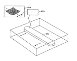
FIGS. 17-20, 17A, 18A, 20A and 21-24 show alternative configurations of magnetrons supported on a
[0043]
FIGS. 17, 17A, 18, 18A, 19, 20, and 20A are a series of related cross-sectional views showing the movement of the end of the
[0044]
In the plan view of FIG. 24, an upper
[0045]
FIGS. 17A, 18A and 20A show examples using four bevels (or cams) 415, 416, 417, 418, which are spring loaded central magnetron connections to the central bearing rail track ( (Not shown). A plan view of the end of the magnetron is shown in FIG. 17A, and two sets of
[0046]
The structure of the magnetron assembly conceptually described above is as shown in FIGS. 25 and 26 as an actual mechanism.
[0047]
FIGS. 25 and 26 are a bottom view and a cross-sectional view of the
[0048]
In traditional configurations, the horizontal behavior of the
[0049]
In this manner, the motion of the magnetron assembly is parallel and uniform for an unsputtered, substantially flat frontal shape before the target is eroded or used. This configuration is used for sputtering relatively small rectangular substrates up to about 400 mm × 500 mm in size.
[0050]
If the magnetron is to be tilted using the configuration according to the present invention, the bearing rails 138, 140 are tilted (eg, as shown by the configuration of FIG. 22) and the central
[0051]
In the method according to the present invention, when the magnetron assembly as shown in FIGS. 25 and 26 is moved laterally along the target assembly, the magnetron assembly is moved vertically. However, given a change in the erosion profile (shape) in the depth direction of the target as shown in FIG. 6, moving the magnetron assembly up and down in parallel can be compared to the current vertically fixed configuration. However, the uniformity of the film thickness and the controllability of the film thickness cannot be improved. In another configuration, each vertical support is driven by an independent motor or actuator to control the vertical movement of the support beam and magnetron assembly in relation to the lateral position of the magnetron assembly. It is also possible to do.
[0052]
[Two parallel beam bearing support]
For larger rectangular substrates of about 600 mm × 700 mm size, the second mechanism outlined in FIGS. 27 and 28 and detailed in FIGS. 34 and 35 is used.
[0053]
FIG. 27 shows the outline of the second mechanism according to the present invention. A
[0054]
The magnetron supported by the end rail is illustrated in FIGS. FIG. 29 shows a cross-sectional view of a process chamber that includes a
[0055]
The detailed views of FIGS. 34 and 35 show a
[0056]
The magnetron assemblies of FIGS. 34 and 35 are supported on bearing
[0057]
[Two piece hinge-coupled magnetron]
FIG. 36 and FIG. 37 show another embodiment of the
[0058]
[Split-type magnetron that follows the reference profile]
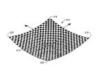
FIG. 38 shows another embodiment according to the present invention. In this embodiment, one or more cam surfaces and cam followers are used to vary the distance between parts of a magnetron assembly having magnetron subsections that can be moved independently of each other and adjacent permanents in the magnetron magnet array. The outer shape in which the magnets draw a continuous loop is maintained. The magnet subsections (a series of magnet member subsections) can be pivotable, can be hinged together like a chain to provide a continuous magnetic field, or flexible It can be housed in a housing. As shown in FIG. 38, several cam surfaces (a series of cam surfaces) form a continuous
[0059]
FIG. 38A shows another configuration according to the present invention. In FIG. 38A, the
[0060]
39 to 42 show three types of ideal surface patterns / profiles available for the
[0061]
The surface pattern / profile in FIG. 39 is similar to the surface pattern / profile tracked by the magnetron assembly configured as shown in FIGS. 9-15 (higher opposing corners and other opposing corners Lower). In this profile, the
[0062]
FIG. 40 shows a two-dimensional circular or parabolic curved surface. The high point of the curved surface or the arc-shaped surface is arranged along the horizontal
[0063]
The profile of the surface profile / pattern shown in FIG. 41 shows a parabolic or circular shape that is open upward, in which all corners are right corner 516, back
[0064]
FIG. 42 shows a concave downward circular or parabolic shape, with the four
[0065]
As those skilled in the art will appreciate, a mechanical cam shape (eg, FIG. 38) or other moderately continuous cam surface profile / pattern may be used between the magnetron subsection and the target assembly. The distance can be changed. However, the surface patterns / profiles shown in the figures are just some of the many surface pattern variations available. Cam face / profile changes can be applied by deforming the cam face accordingly if it is desired to locally change the sputtering at a particular location.
[0066]
[Up / down actuator]
In another configuration of the apparatus according to the present invention, as shown in FIG. 43, a
[0067]
[Electromagnetic magnetron control of sputtering]
44 and 45 show the configuration of a magnetron using an electromagnet that can be used to control sputtering. The
[0068]
FIG. 45 shows a configuration in which an electromagnet is used for the
[0069]
In the method according to the present invention, which selectively controls the thickness of the film formed on the substrate during sputtering, the step of moving the magnet member in the lateral direction in the vicinity of the sputtering target; Changing the strength of the magnetic field when moved in the horizontal direction to promote sputtering on the target surface, and forming a pattern with a specific film thickness on the substrate being processed during sputtering. In some cases, it is desirable to make the film thickness different from making it uniform. For example, it may be desired to increase the thickness of the film at the edge of the substrate in order to increase the durability of the wiring connection with the conductive layer deposited on the substrate and to prevent cracking. In general, regardless of whether local film thickness non-uniformity is desired, it is desirable that errors (tolerances) in film thickness uniformity across almost the entire substrate must be maintained. . According to the configuration and the method of the present invention, it is possible to make the film uniform uniformly at a place where the thickness of the film is desired to be uniform and non-uniform at the place where it is desired to be non-uniform.
[0070]
According to the method of the present invention, the thickness of the membrane is adjusted by moving the magnetron assembly or magnet section laterally and moving at least a part of the magnetron assembly by the vertical support in the height direction according to its horizontal position. Improves uniformity.
[0071]
In the method according to the present invention, the method includes the step of moving the magnet member in the lateral direction in the vicinity of the sputtering target and the step of moving a part of the magnet in the vertical direction, the distance between the reference surface and the predetermined position. By making it larger than the error (tolerance) range of parallelism with the moving plane, the strength of the magnetic field deviating from the plane is changed to improve the control of the film thickness. In another method of the present invention, the step of moving the magnet member in the lateral direction along the track, and moving part of the magnet member in the lateral direction and simultaneously moving in the vertical direction, one along the track. Changing the strength of the magnetic field used for sputtering at the above locations to improve the uniformity or controllability of the film thickness with respect to sputtering. The magnet member is moved laterally along the track, and a part of the magnet member is moved up and down simultaneously with the lateral movement of the magnet member, so that sputtering is performed at one or more points along the track. Thus, the controllability of the thickness of the film formed during sputtering can be improved by changing the strength of the magnetic field used.
[0072]
In the method according to the present invention, the step of changing the strength of the magnetic field includes changing the strength of the electromagnet of the magnet member in accordance with a pattern corresponding to the lateral position of the magnet member.
[0073]
Although the present invention has been described based on specific embodiments as described above, those skilled in the art will recognize that changes may be made in form and detail without departing from the scope and spirit of the invention. Let's go.
[Brief description of the drawings]
FIG. 1 is a schematic plan view of a conventional magnetron apparatus.
2 is a cross-sectional view of a sputtering chamber separated from the prior art magnetron chamber of FIG. 1 by a target assembly.
3 is a side cross-sectional view of the apparatus of FIG. 2 conceptually showing the magnetron magnetic field extending beyond the sputtering target. FIG.
FIG. 4 is a sectional view conceptually showing a magnetron including a permanent magnet and a state in which a magnetic field is generated downward therefrom.
5 is a second side cross-sectional view of the apparatus of FIG. 2, conceptually showing that the magnetic field of the magnetron barely exceeds the sputtering target when the magnetron is lifted to the uppermost position. is there.
FIG. 6 is an erosion profile of a target according to the prior art, showing a pattern of erosion (utilization) of the sputtering target during sputtering.
FIG. 7 shows a film thickness profile on a substrate for a sputtering target using a magnetron chamber according to the prior art, and analyzed by a sheet resistance value (inversely proportional to the film thickness) measured using a five-point probe. It is a figure which shows the obtained profile.
FIG. 8 is a contour plot of the film thickness of a sputtering target assembly when using the configuration and method of the present invention, and analysis of sheet resistance (in inverse proportion to film thickness) measured using a five-point probe. It is a figure which shows the contour-line plot from.
FIG. 9 is a schematic perspective view showing a magnetron chamber using a central bearing rail to support the magnetron.
FIG. 10 is a schematic diagram showing the central magnetron support beam of FIG. 9 exaggerated in dimension, and showing how the support beam twists when the support beam moves along the central beam support.
11 is a cross-sectional view taken along line 11-11 of the magnetron support beam of FIG.
12 is a cross-sectional view taken along line 12-12 of the magnetron support beam of FIG.
13 is a cross-sectional view taken along line 13-13 of the magnetron support beam of FIG.
FIG. 14 is a plan view of a magnetron chamber according to the present invention comprising a central magnetron support beam.
15 is a perspective view showing a bearing channel beam including a bearing track (rail) supported by a central beam as shown in FIG. 9, for example.
FIG. 16 is a view showing an improved bearing support rail, in which a channel is divided and one of both ends of the channel is lifted to move a part of the magnetron up and down. It is.
17 is a plan view showing an end portion of the magnetron shown in FIG. 18, and is a view showing a state in which it is about to be lifted by engaging with a slope (cam).
17A is a plan view showing an end portion of the magnetron shown in FIG. 18A, and shows a state in which the magnetron is about to be lifted by being engaged with a slope (cam). FIG.
FIG. 18 is a partial cross-sectional view of the magnetron chamber taken along line 18-18 in FIGS. 20 and 24, and shows that the end of the magnetron is lifted by the inclined surface at the end of the chamber.
FIG. 18A is a partial cross-sectional view of the magnetron chamber taken along
FIG. 19 is a sectional side view showing a positional relationship between a magnetron and a slope.
FIG. 20 is a plan view of a magnetron chamber showing the end of the magnetron lifted by the slopes of the opposite corners.
FIG. 20A is a plan view of a magnetron chamber showing the end of the magnetron lifted by the slope of each corner.
FIG. 21 is a schematic cross-sectional view taken along line 21-21 in FIG. 24 and shows a state in which the end of a deformable horizontal magnetron is warped to form a curved shape.
FIG. 21A is a schematic cross-sectional view taken along line 21-21 in FIG. 24 and shows a state where the end of a rigid horizontal magnetron is lifted.
22 is a schematic cross-sectional view taken along line 22-22 in FIG. 24, and is a view showing a deformable horizontal magnetron.
22A is a schematic cross-sectional view taken along line 22-22 in FIG. 24, and shows a rigid horizontal magnetron. FIG.
FIG. 23 is a schematic cross-sectional view taken along line 23-23 in FIG. 24 and shows a state in which the end of a deformable horizontal magnetron is warped up.
FIG. 23A is a schematic cross-sectional view taken along line 23-23 in FIG. 24 and shows a state where the end of a rigid horizontal magnetron is lifted.
FIG. 24 is a schematic plan view of a magnetron chamber, in which the magnetron is supported in the vicinity of the center, and inclined surfaces are provided at opposite corners so that when the magnetron approaches either end, the magnetron It is a figure which shows what the position of the up-down direction of the edge part is variable.
FIG. 25 is a bottom view of a magnetron chamber when a central support beam is used for a magnetron track.
26 is a cross-sectional view showing the magnetron chamber of FIG. 25. FIG.
FIG. 27 is a schematic perspective view of a magnetron chamber showing an internal movable magnetron supported by two horizontal beams near both ends.
28 is an explanatory view schematically showing how the height of the magnetron changes (tilts) as the magnetron moves from one end to the other end along the inclined orbit as shown in FIG. 27;
FIG. 29 is a schematic cross-sectional view showing a magnetron supported by two substantially parallel rails (tracks) according to the present invention.
30 is a cross-sectional view taken along line 30-30 in FIG. 33, showing the behavior of the magnetron support rail and the magnetron.
FIG. 31 is a cross-sectional view taken along line 31-31 in FIG. 33, showing the behavior of the magnetron support rail and the magnetron.
32 is a cross-sectional view taken along line 32-32 in FIG. 33, showing the behavior of the magnetron support rail and the magnetron.
FIG. 33 is a schematic plan view of a magnetron chamber, showing a state in which the magnetron is supported near two ends by two horizontal support rails.
FIG. 34 is a bottom view of the magnetron, showing the state where the magnetron is supported at the edge of the magnetron chamber by two substantially parallel beams.
35 is a cross-sectional view of FIG. 34. FIG.
FIG. 36 is a cross-sectional view showing a hinge-coupled magnetron provided in a magnetron chamber, for example, as shown in FIG.
FIG. 37 is a schematic perspective view showing a hinged magnetron and a bowed central track according to the present invention.
FIG. 38 is a diagram illustrating a state in which a magnetron assembly (apparatus) having a permanent magnet subsection (subcomponent) moves, and the target being sputtered and each magnet subsection as the magnetron moves laterally; It is the figure which shows the place where the up-down direction movement of each magnet subsection is influenced by the outline board which changes the up-down direction space between them.
FIG. 38A is a diagram illustrating a state in which a magnetron assembly (device) having a deformable magnetron coupled to a contour plate via several cam follower links moves, and when the magnetron moves laterally; , Showing that the vertical movement of said part of the magnetron is affected by the contour plate that changes the vertical distance between the target being sputtered and each part of the magnetron (the part connected to the cam follower ring) It is a figure.
FIG. 39 is a diagram conceptually showing a magnetron reference plane pattern for a contour plate in a checkered pattern, showing that the right and left corners are raised and the front and rear corners are lowered. FIG.
FIG. 40 is a diagram conceptually showing a magnet reference plane, which is bent downward in a parabolic shape or an arc shape with respect to a horizontal central axis, and all trajectories orthogonal to the horizontal axis are equal. It is a figure which shows what is.
41 is a diagram conceptually showing a bowl-shaped parabolic pattern plate used as a magnet section guide (magnet component portion guide), which has the same shape as that shown in FIG. FIG.
FIG. 42 is a diagram conceptually showing a convex reference surface pattern used as a magnet pattern contour plate.
FIG. 43 shows a flat magnet contour plate assembly using an activator for individually moving up and down a magnet section using an electrical activator or other activator according to a pre-programmed pattern.
FIG. 44 is a diagram showing a magnetron in which the magnet is an electromagnet, where the magnetic field is changed by changing the strength of the electrical energy supplied to each of the magnetron's electromagnet segments when the magnetron moves horizontally during sputtering. It is the figure which shows what controls the intensity of.
45 is a cross-sectional view of an electromagnet magnetron according to the present invention used in the configuration shown in FIG. 44. FIG.
Claims (9)
前記レールは、前記トラックが前記一連のレールの第1の端部から前記一連のレールの第2の端部に移動する際に前記トラックの略一定の軌道幅を可能とするよう、互いに隣接して延びており、
スパッタリング中に、基板と前記磁石部材との間に配置されたターゲットに対向する前記基板上にスパッタリング成膜された膜の厚さの均一性を改善するために、前記磁石部材が前記一連のレールの前記第1の端部から前記一連のレールの前記第2の端部に移動する際における前記磁石部材の前記移動によって、前記磁石部材が前記移動中に傾けられる、磁石スキャニング機構。A magnet scanning mechanism comprising a magnet member supported on a series of rails and functioning as a track moving on the series of rails,
The rails are adjacent to each other so as to allow a substantially constant track width of the tracks as the tracks move from a first end of the series of rails to a second end of the series of rails. Extending,
In order to improve the uniformity of the thickness of the sputtered film on the substrate facing the target disposed between the substrate and the magnet member during sputtering, the magnet member is connected to the series of rails. A magnet scanning mechanism in which the magnet member is tilted during the movement by the movement of the magnet member when moving from the first end to the second end of the series of rails.
スパッタリング中に、基板と前記磁石部材との間に配置されたターゲットに対向する前記基板上にスパッタリング成膜された膜の厚さの均一性を改善するために、前記一組のベアリングレールにおける第1のレールの第1の端部が、前記一組のベアリングレールにおける前記第1のレールの第2の端部よりも前記ターゲットから離れるよう持ち上げられている、磁石スキャニング装置。A magnet scanning device comprising a magnet member that moves as a track on a set of mutually independent linear bearing rails arranged substantially in parallel,
In order to improve the uniformity of the thickness of the sputtered film on the substrate facing the target disposed between the substrate and the magnet member during sputtering, the first set of bearing rails A magnet scanning device, wherein a first end of one rail is lifted away from the target relative to a second end of the first rail in the set of bearing rails.
前記マグネトロンは、前記マグネトロンと前記ターゲットの間に前記第1の方向に対して垂直な第2の方向に沿って可変する高さを与えるように可撓性を有し、これにより前記基板にスパッタリング成膜された膜の厚さの均一性を改善する、磁石スキャニング装置。 The magnetron is flexible to provide a variable height between the magnetron and the target along a second direction perpendicular to the first direction, thereby sputtering the substrate. A magnet scanning device that improves the uniformity of the thickness of the deposited film.
Applications Claiming Priority (2)
| Application Number | Priority Date | Filing Date | Title |
|---|---|---|---|
| US08/684,446 US5855744A (en) | 1996-07-19 | 1996-07-19 | Non-planar magnet tracking during magnetron sputtering |
| US08/684446 | 1996-07-19 |
Publications (2)
| Publication Number | Publication Date |
|---|---|
| JPH1096078A JPH1096078A (en) | 1998-04-14 |
| JP4054411B2 true JP4054411B2 (en) | 2008-02-27 |
Family
ID=24748082
Family Applications (1)
| Application Number | Title | Priority Date | Filing Date |
|---|---|---|---|
| JP22697197A Expired - Lifetime JP4054411B2 (en) | 1996-07-19 | 1997-07-18 | Non-planar magnet tracking during magnetron sputtering. |
Country Status (5)
| Country | Link |
|---|---|
| US (1) | US5855744A (en) |
| EP (1) | EP0820088A3 (en) |
| JP (1) | JP4054411B2 (en) |
| KR (1) | KR100472811B1 (en) |
| TW (1) | TW425590B (en) |
Cited By (1)
| Publication number | Priority date | Publication date | Assignee | Title |
|---|---|---|---|---|
| US8512527B2 (en) | 2010-08-11 | 2013-08-20 | Samsung Display Co., Ltd. | Magnet transportation system, sputtering apparatus including the same and sputtering method |
Families Citing this family (87)
| Publication number | Priority date | Publication date | Assignee | Title |
|---|---|---|---|---|
| US5873989A (en) * | 1997-02-06 | 1999-02-23 | Intevac, Inc. | Methods and apparatus for linear scan magnetron sputtering |
| EP0918351A1 (en) * | 1997-11-19 | 1999-05-26 | Sinvaco N.V. | Improved planar magnetron with moving magnet assembly |
| US6258217B1 (en) | 1999-09-29 | 2001-07-10 | Plasma-Therm, Inc. | Rotating magnet array and sputter source |
| US6267851B1 (en) * | 1999-10-28 | 2001-07-31 | Applied Komatsu Technology, Inc. | Tilted sputtering target with shield to block contaminants |
| AU1786301A (en) * | 1999-12-02 | 2001-06-12 | Tegal Corporation | Improved reactor with heated and textured electrodes and surfaces |
| US6436252B1 (en) | 2000-04-07 | 2002-08-20 | Surface Engineered Products Corp. | Method and apparatus for magnetron sputtering |
| US6585870B1 (en) | 2000-04-28 | 2003-07-01 | Honeywell International Inc. | Physical vapor deposition targets having crystallographic orientations |
| US6506289B2 (en) * | 2000-08-07 | 2003-01-14 | Symmorphix, Inc. | Planar optical devices and methods for their manufacture |
| JP2002091512A (en) * | 2000-09-12 | 2002-03-29 | Meidensha Corp | Programming support device for sequencer |
| US6533907B2 (en) | 2001-01-19 | 2003-03-18 | Symmorphix, Inc. | Method of producing amorphous silicon for hard mask and waveguide applications |
| US7469558B2 (en) * | 2001-07-10 | 2008-12-30 | Springworks, Llc | As-deposited planar optical waveguides with low scattering loss and methods for their manufacture |
| GB0118803D0 (en) * | 2001-08-02 | 2001-09-26 | Bekaert Sa Nv | Adjustable magnet configuration and method for magnetron sputtering |
| US7404877B2 (en) * | 2001-11-09 | 2008-07-29 | Springworks, Llc | Low temperature zirconia based thermal barrier layer by PVD |
| US7378356B2 (en) * | 2002-03-16 | 2008-05-27 | Springworks, Llc | Biased pulse DC reactive sputtering of oxide films |
| US6884327B2 (en) | 2002-03-16 | 2005-04-26 | Tao Pan | Mode size converter for a planar waveguide |
| TW574407B (en) * | 2002-06-18 | 2004-02-01 | Hannstar Display Corp | Magnetron oscillatory scanning-type sputtering device |
| US20070264564A1 (en) | 2006-03-16 | 2007-11-15 | Infinite Power Solutions, Inc. | Thin film battery on an integrated circuit or circuit board and method thereof |
| US8445130B2 (en) * | 2002-08-09 | 2013-05-21 | Infinite Power Solutions, Inc. | Hybrid thin-film battery |
| US8404376B2 (en) | 2002-08-09 | 2013-03-26 | Infinite Power Solutions, Inc. | Metal film encapsulation |
| US8021778B2 (en) * | 2002-08-09 | 2011-09-20 | Infinite Power Solutions, Inc. | Electrochemical apparatus with barrier layer protected substrate |
| US8431264B2 (en) * | 2002-08-09 | 2013-04-30 | Infinite Power Solutions, Inc. | Hybrid thin-film battery |
| US8394522B2 (en) * | 2002-08-09 | 2013-03-12 | Infinite Power Solutions, Inc. | Robust metal film encapsulation |
| US8535396B2 (en) * | 2002-08-09 | 2013-09-17 | Infinite Power Solutions, Inc. | Electrochemical apparatus with barrier layer protected substrate |
| US8236443B2 (en) * | 2002-08-09 | 2012-08-07 | Infinite Power Solutions, Inc. | Metal film encapsulation |
| TWI274199B (en) * | 2002-08-27 | 2007-02-21 | Symmorphix Inc | Optically coupling into highly uniform waveguides |
| KR20040057287A (en) * | 2002-12-26 | 2004-07-02 | 삼성전자주식회사 | target for sputtering |
| US6905579B2 (en) * | 2003-02-13 | 2005-06-14 | Sputtering Components, Inc. | Cylindrical magnetron target and spindle apparatus |
| CN1756856B (en) | 2003-02-27 | 2011-10-12 | 希莫菲克斯公司 | Dielectric barrier layer films |
| US7238628B2 (en) * | 2003-05-23 | 2007-07-03 | Symmorphix, Inc. | Energy conversion and storage films and devices by physical vapor deposition of titanium and titanium oxides and sub-oxides |
| US8728285B2 (en) * | 2003-05-23 | 2014-05-20 | Demaray, Llc | Transparent conductive oxides |
| US20050133361A1 (en) * | 2003-12-12 | 2005-06-23 | Applied Materials, Inc. | Compensation of spacing between magnetron and sputter target |
| US20060049040A1 (en) * | 2004-01-07 | 2006-03-09 | Applied Materials, Inc. | Apparatus and method for two dimensional magnetron scanning for sputtering onto flat panels |
| US8500975B2 (en) * | 2004-01-07 | 2013-08-06 | Applied Materials, Inc. | Method and apparatus for sputtering onto large flat panels |
| US7513982B2 (en) * | 2004-01-07 | 2009-04-07 | Applied Materials, Inc. | Two dimensional magnetron scanning for flat panel sputtering |
| US7556718B2 (en) * | 2004-06-22 | 2009-07-07 | Tokyo Electron Limited | Highly ionized PVD with moving magnetic field envelope for uniform coverage of feature structure and wafer |
| BRPI0516204A (en) * | 2004-09-28 | 2008-08-26 | Oc Oerlikon Balzers Ag | process for producing magnetron coated substrates and magnetron spray source |
| US8778144B2 (en) * | 2004-09-28 | 2014-07-15 | Oerlikon Advanced Technologies Ag | Method for manufacturing magnetron coated substrates and magnetron sputter source |
| US8636876B2 (en) * | 2004-12-08 | 2014-01-28 | R. Ernest Demaray | Deposition of LiCoO2 |
| US7959769B2 (en) * | 2004-12-08 | 2011-06-14 | Infinite Power Solutions, Inc. | Deposition of LiCoO2 |
| EP1710829A1 (en) | 2005-04-05 | 2006-10-11 | Applied Films GmbH & Co. KG | Magnet assembly for a planar magnetron |
| US20060272935A1 (en) * | 2005-06-06 | 2006-12-07 | Applied Materials, Inc. | Multiple scanning magnetrons |
| JP4923450B2 (en) * | 2005-07-01 | 2012-04-25 | 富士ゼロックス株式会社 | Batch processing support apparatus and method, program |
| US20070012663A1 (en) * | 2005-07-13 | 2007-01-18 | Akihiro Hosokawa | Magnetron sputtering system for large-area substrates having removable anodes |
| US20070012558A1 (en) * | 2005-07-13 | 2007-01-18 | Applied Materials, Inc. | Magnetron sputtering system for large-area substrates |
| US20070084720A1 (en) * | 2005-07-13 | 2007-04-19 | Akihiro Hosokawa | Magnetron sputtering system for large-area substrates having removable anodes |
| US20070012559A1 (en) * | 2005-07-13 | 2007-01-18 | Applied Materials, Inc. | Method of improving magnetron sputtering of large-area substrates using a removable anode |
| US7838133B2 (en) * | 2005-09-02 | 2010-11-23 | Springworks, Llc | Deposition of perovskite and other compound ceramic films for dielectric applications |
| US20070051616A1 (en) * | 2005-09-07 | 2007-03-08 | Le Hienminh H | Multizone magnetron assembly |
| US7588668B2 (en) | 2005-09-13 | 2009-09-15 | Applied Materials, Inc. | Thermally conductive dielectric bonding of sputtering targets using diamond powder filler or thermally conductive ceramic fillers |
| US20070056843A1 (en) * | 2005-09-13 | 2007-03-15 | Applied Materials, Inc. | Method of processing a substrate using a large-area magnetron sputtering chamber with individually controlled sputtering zones |
| US20070056850A1 (en) * | 2005-09-13 | 2007-03-15 | Applied Materials, Inc. | Large-area magnetron sputtering chamber with individually controlled sputtering zones |
| US7879210B2 (en) * | 2006-02-03 | 2011-02-01 | Applied Materials, Inc. | Partially suspended rolling magnetron |
| WO2007059347A2 (en) * | 2005-11-17 | 2007-05-24 | Applied Materials, Inc. | Flexible magnetron including partial rolling support and centering pins |
| US8961756B2 (en) * | 2006-08-04 | 2015-02-24 | Applied Materials, Inc. | Ganged scanning of multiple magnetrons, especially two level folded magnetrons |
| KR100910673B1 (en) * | 2006-08-04 | 2009-08-04 | 어플라이드 머티어리얼스, 인코포레이티드 | Ganged scanning of multiple magnetrons, especially two level folded magnetrons |
| US8062708B2 (en) * | 2006-09-29 | 2011-11-22 | Infinite Power Solutions, Inc. | Masking of and material constraint for depositing battery layers on flexible substrates |
| US8197781B2 (en) * | 2006-11-07 | 2012-06-12 | Infinite Power Solutions, Inc. | Sputtering target of Li3PO4 and method for producing same |
| EP1923902B2 (en) * | 2006-11-14 | 2014-07-23 | Applied Materials, Inc. | Magnetron sputtering source, sputter coating system and method for coating a substrate |
| US20080296142A1 (en) * | 2007-05-29 | 2008-12-04 | Hien-Minh Huu Le | Swinging magnets to improve target utilization |
| JP5140383B2 (en) * | 2007-11-07 | 2013-02-06 | 株式会社アルバック | Sputtering equipment |
| KR20100102101A (en) * | 2007-11-07 | 2010-09-20 | 어플라이드 머티어리얼스, 인코포레이티드 | Sputter coating device and coating method |
| US9334557B2 (en) * | 2007-12-21 | 2016-05-10 | Sapurast Research Llc | Method for sputter targets for electrolyte films |
| US8268488B2 (en) | 2007-12-21 | 2012-09-18 | Infinite Power Solutions, Inc. | Thin film electrolyte for thin film batteries |
| JP5705549B2 (en) | 2008-01-11 | 2015-04-22 | インフィニット パワー ソリューションズ, インコーポレイテッド | Thin film encapsulation for thin film batteries and other devices |
| CN201162043Y (en) * | 2008-03-21 | 2008-12-10 | 北京京东方光电科技有限公司 | Magnetron sputtering target structure and equipment |
| CN101983469B (en) * | 2008-04-02 | 2014-06-04 | 无穷动力解决方案股份有限公司 | Passive over/under voltage control and protection for energy storage devices associated with energy harvesting |
| US8500962B2 (en) * | 2008-07-21 | 2013-08-06 | Ascentool Inc | Deposition system and methods having improved material utilization |
| EP2319101B1 (en) | 2008-08-11 | 2015-11-04 | Sapurast Research LLC | Energy device with integral collector surface for electromagnetic energy harvesting and method thereof |
| JP5650646B2 (en) * | 2008-09-12 | 2015-01-07 | インフィニット パワー ソリューションズ, インコーポレイテッド | Energy device with integral conductive surface for data communication via electromagnetic energy and method for data communication via electromagnetic energy |
| US8508193B2 (en) * | 2008-10-08 | 2013-08-13 | Infinite Power Solutions, Inc. | Environmentally-powered wireless sensor module |
| KR20120025521A (en) * | 2009-05-20 | 2012-03-15 | 인피니트 파워 솔루션스, 인크. | Method of integrating electrochemical devices into and onto fixtures |
| CN101988188B (en) * | 2009-07-30 | 2013-08-28 | 鸿富锦精密工业(深圳)有限公司 | Magnetic control device for sputtering |
| EP2474056B1 (en) * | 2009-09-01 | 2016-05-04 | Sapurast Research LLC | Printed circuit board with integrated thin film battery |
| US20110300432A1 (en) | 2010-06-07 | 2011-12-08 | Snyder Shawn W | Rechargeable, High-Density Electrochemical Device |
| US9017554B2 (en) | 2010-08-27 | 2015-04-28 | Xylem Water Solutions Zelienople Llc | Handle for underdrain |
| US9085821B2 (en) | 2011-12-14 | 2015-07-21 | Intermolecular, Inc. | Sputter gun having variable magnetic strength |
| CN103074587B (en) * | 2013-02-01 | 2014-10-15 | 湘潭宏大真空技术股份有限公司 | Adjusting device and adjusting method for large-area continuous magnetron sputtering coating uniformity |
| CN103849846B (en) * | 2014-03-07 | 2015-12-09 | 东莞鑫泰玻璃科技有限公司 | Magnet regulating mechanism |
| US20160133446A1 (en) * | 2014-11-12 | 2016-05-12 | Proportional Technologies, Inc. | Moving magnet assembly to increase the utility of a rectangular magnetron sputtering target |
| CN105088159B (en) * | 2015-08-12 | 2018-08-03 | 京东方科技集团股份有限公司 | A kind of magnetic control sputtering device |
| US20190144990A1 (en) * | 2017-11-16 | 2019-05-16 | Oliver James Groves | Device For Sputtering A Material Onto A Surface Of A Substrate While Moving |
| US11462394B2 (en) * | 2018-09-28 | 2022-10-04 | Taiwan Semiconductor Manufacturing Co., Ltd. | Physical vapor deposition apparatus and method thereof |
| EP4012066A4 (en) * | 2019-08-08 | 2023-08-09 | Tokyo Electron Limited | Film forming apparatus and film forming method |
| EP4246883A1 (en) | 2022-03-15 | 2023-09-20 | Deutsche Telekom AG | Techniques to decrease the level of encryption in a trusted communication environment |
| CN116092899B (en) * | 2023-01-16 | 2024-01-09 | 深圳市矩阵多元科技有限公司 | Scanning magnetron device for PVD planar target and magnetron sputtering equipment |
| KR102625287B1 (en) | 2023-02-23 | 2024-01-15 | 전병률 | Functional pillow with adjustable height and back and forth |
| CN116445874B (en) * | 2023-05-09 | 2023-09-05 | 宁波招宝磁业有限公司 | Magnetron sputtering target device for neodymium-iron-boron magnet |
Family Cites Families (10)
| Publication number | Priority date | Publication date | Assignee | Title |
|---|---|---|---|---|
| DE2707144A1 (en) * | 1976-02-19 | 1977-08-25 | Sloan Technology Corp | Cathode sputtering device with magnetic equipment - which can be displaced to move the area of sputtering over an extended surface by relative movement |
| JPS6134177A (en) * | 1984-07-25 | 1986-02-18 | Tokuda Seisakusho Ltd | Magnet driving device |
| JPH02290971A (en) * | 1989-04-28 | 1990-11-30 | Tokyo Electron Ltd | Sputtering device |
| JPH03243762A (en) * | 1990-02-20 | 1991-10-30 | Fujitsu Ltd | Magnetron sputtering device |
| US5079481A (en) * | 1990-08-02 | 1992-01-07 | Texas Instruments Incorporated | Plasma-assisted processing magneton with magnetic field adjustment |
| KR950000906B1 (en) * | 1991-08-02 | 1995-02-03 | 니찌덴 아넬바 가부시기가이샤 | Sputtering apparatus |
| US5262030A (en) * | 1992-01-15 | 1993-11-16 | Alum Rock Technology | Magnetron sputtering cathode with electrically variable source size and location for coating multiple substrates |
| JPH05202471A (en) * | 1992-01-28 | 1993-08-10 | Fujitsu Ltd | Magnetron sputtering apparatus |
| US5328585A (en) * | 1992-12-11 | 1994-07-12 | Photran Corporation | Linear planar-magnetron sputtering apparatus with reciprocating magnet-array |
| JPH07166346A (en) * | 1993-12-13 | 1995-06-27 | Ulvac Japan Ltd | Magnetron sputtering device |
-
1996
- 1996-07-19 US US08/684,446 patent/US5855744A/en not_active Expired - Lifetime
-
1997
- 1997-07-16 EP EP97305316A patent/EP0820088A3/en not_active Withdrawn
- 1997-07-18 TW TW086110225A patent/TW425590B/en not_active IP Right Cessation
- 1997-07-18 JP JP22697197A patent/JP4054411B2/en not_active Expired - Lifetime
- 1997-07-19 KR KR1019970034127A patent/KR100472811B1/en not_active IP Right Cessation
Cited By (1)
| Publication number | Priority date | Publication date | Assignee | Title |
|---|---|---|---|---|
| US8512527B2 (en) | 2010-08-11 | 2013-08-20 | Samsung Display Co., Ltd. | Magnet transportation system, sputtering apparatus including the same and sputtering method |
Also Published As
| Publication number | Publication date |
|---|---|
| JPH1096078A (en) | 1998-04-14 |
| KR100472811B1 (en) | 2005-07-04 |
| US5855744A (en) | 1999-01-05 |
| TW425590B (en) | 2001-03-11 |
| EP0820088A2 (en) | 1998-01-21 |
| KR980012090A (en) | 1998-04-30 |
| EP0820088A3 (en) | 2000-10-25 |
Similar Documents
| Publication | Publication Date | Title |
|---|---|---|
| JP4054411B2 (en) | Non-planar magnet tracking during magnetron sputtering. | |
| EP2204469A1 (en) | Magnetron unit, magnetron sputtering apparatus and method for manufacturing electronic device | |
| US8500975B2 (en) | Method and apparatus for sputtering onto large flat panels | |
| US7982195B2 (en) | Controlled dose ion implantation | |
| US8455837B2 (en) | Ion implanter, ion implantation method and program | |
| TWI443716B (en) | Method of performing high-tilt implantation, apparatus for implanting ions and method of implanting workpiece | |
| US20030197133A1 (en) | Method and apparatus for scanning a workpiece in a vacuum chamber | |
| US20170098458A1 (en) | Ion beam etching method and ion beam etching apparatus | |
| CN112639164B (en) | Coaxial lifting device with dynamic leveling function | |
| KR900005219B1 (en) | Ion beam implanter control system and method | |
| US9376731B2 (en) | Magneto-thermal processing apparatus and methods | |
| WO2013179548A1 (en) | Magnetron sputtering device, magnetron sputtering method, and storage medium | |
| TWI732447B (en) | Scan robot for semiconductor wafer ion implantation | |
| KR100689673B1 (en) | Method for nonuniformity implant in semiconductor device | |
| US6464841B1 (en) | Cathode having variable magnet configuration | |
| JP6567119B1 (en) | Substrate processing apparatus, control method therefor, film forming apparatus, and electronic component manufacturing method | |
| US9410234B2 (en) | Sputtering device and method of forming layer using the same | |
| CN111373505A (en) | Magnet assembly of magnetron sputtering device | |
| CN114823307A (en) | Semiconductor annealing method, annealing device and annealing system | |
| JP2002235168A (en) | Method and apparatus for film deposition | |
| KR100437867B1 (en) | Cathode having variable magnet configuration | |
| KR20200051947A (en) | Sputtering apparatus | |
| KR20090058993A (en) | Magnetron sputtering apparatus and method for driving the same | |
| JP2022117719A (en) | Sputtering device and sputtering method | |
| JPH1121666A (en) | Magnetron cathode for sputtering device |
Legal Events
| Date | Code | Title | Description |
|---|---|---|---|
| A621 | Written request for application examination |
Free format text: JAPANESE INTERMEDIATE CODE: A621 Effective date: 20040713 |
|
| A977 | Report on retrieval |
Free format text: JAPANESE INTERMEDIATE CODE: A971007 Effective date: 20070521 |
|
| A131 | Notification of reasons for refusal |
Free format text: JAPANESE INTERMEDIATE CODE: A131 Effective date: 20070529 |
|
| A521 | Request for written amendment filed |
Free format text: JAPANESE INTERMEDIATE CODE: A523 Effective date: 20070726 |
|
| A131 | Notification of reasons for refusal |
Free format text: JAPANESE INTERMEDIATE CODE: A131 Effective date: 20070821 |
|
| A521 | Request for written amendment filed |
Free format text: JAPANESE INTERMEDIATE CODE: A523 Effective date: 20071018 |
|
| TRDD | Decision of grant or rejection written | ||
| A01 | Written decision to grant a patent or to grant a registration (utility model) |
Free format text: JAPANESE INTERMEDIATE CODE: A01 Effective date: 20071113 |
|
| A61 | First payment of annual fees (during grant procedure) |
Free format text: JAPANESE INTERMEDIATE CODE: A61 Effective date: 20071210 |
|
| FPAY | Renewal fee payment (event date is renewal date of database) |
Free format text: PAYMENT UNTIL: 20101214 Year of fee payment: 3 |
|
| R150 | Certificate of patent or registration of utility model |
Free format text: JAPANESE INTERMEDIATE CODE: R150 |
|
| FPAY | Renewal fee payment (event date is renewal date of database) |
Free format text: PAYMENT UNTIL: 20101214 Year of fee payment: 3 |
|
| FPAY | Renewal fee payment (event date is renewal date of database) |
Free format text: PAYMENT UNTIL: 20111214 Year of fee payment: 4 |
|
| FPAY | Renewal fee payment (event date is renewal date of database) |
Free format text: PAYMENT UNTIL: 20111214 Year of fee payment: 4 |
|
| RD02 | Notification of acceptance of power of attorney |
Free format text: JAPANESE INTERMEDIATE CODE: R3D02 |
|
| FPAY | Renewal fee payment (event date is renewal date of database) |
Free format text: PAYMENT UNTIL: 20111214 Year of fee payment: 4 |
|
| FPAY | Renewal fee payment (event date is renewal date of database) |
Free format text: PAYMENT UNTIL: 20121214 Year of fee payment: 5 |
|
| FPAY | Renewal fee payment (event date is renewal date of database) |
Free format text: PAYMENT UNTIL: 20131214 Year of fee payment: 6 |
|
| R250 | Receipt of annual fees |
Free format text: JAPANESE INTERMEDIATE CODE: R250 |
|
| R250 | Receipt of annual fees |
Free format text: JAPANESE INTERMEDIATE CODE: R250 |
|
| R250 | Receipt of annual fees |
Free format text: JAPANESE INTERMEDIATE CODE: R250 |
|
| R250 | Receipt of annual fees |
Free format text: JAPANESE INTERMEDIATE CODE: R250 |
|
| EXPY | Cancellation because of completion of term |