JP4054093B2 - Semiconductor device - Google Patents
Semiconductor device Download PDFInfo
- Publication number
- JP4054093B2 JP4054093B2 JP27713397A JP27713397A JP4054093B2 JP 4054093 B2 JP4054093 B2 JP 4054093B2 JP 27713397 A JP27713397 A JP 27713397A JP 27713397 A JP27713397 A JP 27713397A JP 4054093 B2 JP4054093 B2 JP 4054093B2
- Authority
- JP
- Japan
- Prior art keywords
- region
- input
- node
- voltage
- nmos transistor
- Prior art date
- Legal status (The legal status is an assumption and is not a legal conclusion. Google has not performed a legal analysis and makes no representation as to the accuracy of the status listed.)
- Expired - Fee Related
Links
- 239000004065 semiconductor Substances 0.000 title claims description 36
- 239000000758 substrate Substances 0.000 claims description 33
- 230000002441 reversible effect Effects 0.000 claims description 22
- 239000010408 film Substances 0.000 description 78
- XUIMIQQOPSSXEZ-UHFFFAOYSA-N Silicon Chemical compound [Si] XUIMIQQOPSSXEZ-UHFFFAOYSA-N 0.000 description 58
- 229910052710 silicon Inorganic materials 0.000 description 58
- 239000010703 silicon Substances 0.000 description 58
- 229910052782 aluminium Inorganic materials 0.000 description 46
- 239000010409 thin film Substances 0.000 description 45
- 238000009792 diffusion process Methods 0.000 description 44
- XAGFODPZIPBFFR-UHFFFAOYSA-N aluminium Chemical compound [Al] XAGFODPZIPBFFR-UHFFFAOYSA-N 0.000 description 42
- 239000003990 capacitor Substances 0.000 description 38
- 230000015556 catabolic process Effects 0.000 description 37
- 239000012535 impurity Substances 0.000 description 32
- 230000015572 biosynthetic process Effects 0.000 description 23
- 239000011229 interlayer Substances 0.000 description 22
- 230000001681 protective effect Effects 0.000 description 20
- 239000010410 layer Substances 0.000 description 19
- 238000010586 diagram Methods 0.000 description 16
- 230000008878 coupling Effects 0.000 description 12
- 238000010168 coupling process Methods 0.000 description 12
- 238000005859 coupling reaction Methods 0.000 description 12
- 229910021332 silicide Inorganic materials 0.000 description 12
- FVBUAEGBCNSCDD-UHFFFAOYSA-N silicide(4-) Chemical group [Si-4] FVBUAEGBCNSCDD-UHFFFAOYSA-N 0.000 description 12
- 230000000694 effects Effects 0.000 description 7
- 238000000034 method Methods 0.000 description 6
- 229910021420 polycrystalline silicon Inorganic materials 0.000 description 6
- 229920005591 polysilicon Polymers 0.000 description 6
- 230000002829 reductive effect Effects 0.000 description 5
- AZDRQVAHHNSJOQ-UHFFFAOYSA-N alumane Chemical compound [AlH3] AZDRQVAHHNSJOQ-UHFFFAOYSA-N 0.000 description 4
- 230000006378 damage Effects 0.000 description 4
- 230000007423 decrease Effects 0.000 description 4
- 230000036961 partial effect Effects 0.000 description 4
- 230000006866 deterioration Effects 0.000 description 3
- 238000009825 accumulation Methods 0.000 description 2
- 239000012141 concentrate Substances 0.000 description 2
- 238000006731 degradation reaction Methods 0.000 description 2
- 239000007772 electrode material Substances 0.000 description 2
- 230000003071 parasitic effect Effects 0.000 description 2
- 230000000644 propagated effect Effects 0.000 description 2
- 238000004080 punching Methods 0.000 description 2
- 241001391944 Commicarpus scandens Species 0.000 description 1
- 230000002411 adverse Effects 0.000 description 1
- 239000013078 crystal Substances 0.000 description 1
- 230000007547 defect Effects 0.000 description 1
- 230000003111 delayed effect Effects 0.000 description 1
- 238000000151 deposition Methods 0.000 description 1
- 230000005611 electricity Effects 0.000 description 1
- 238000005530 etching Methods 0.000 description 1
- 238000004880 explosion Methods 0.000 description 1
- 239000012212 insulator Substances 0.000 description 1
- 238000002955 isolation Methods 0.000 description 1
- 230000000670 limiting effect Effects 0.000 description 1
- 239000000463 material Substances 0.000 description 1
- 238000000059 patterning Methods 0.000 description 1
- 230000001902 propagating effect Effects 0.000 description 1
- 230000003068 static effect Effects 0.000 description 1
Images


Classifications
-
- H—ELECTRICITY
- H01—ELECTRIC ELEMENTS
- H01L—SEMICONDUCTOR DEVICES NOT COVERED BY CLASS H10
- H01L27/00—Devices consisting of a plurality of semiconductor or other solid-state components formed in or on a common substrate
- H01L27/02—Devices consisting of a plurality of semiconductor or other solid-state components formed in or on a common substrate including semiconductor components specially adapted for rectifying, oscillating, amplifying or switching and having potential barriers; including integrated passive circuit elements having potential barriers
- H01L27/0203—Particular design considerations for integrated circuits
- H01L27/0248—Particular design considerations for integrated circuits for electrical or thermal protection, e.g. electrostatic discharge [ESD] protection
- H01L27/0251—Particular design considerations for integrated circuits for electrical or thermal protection, e.g. electrostatic discharge [ESD] protection for MOS devices
- H01L27/0266—Particular design considerations for integrated circuits for electrical or thermal protection, e.g. electrostatic discharge [ESD] protection for MOS devices using field effect transistors as protective elements
-
- H—ELECTRICITY
- H01—ELECTRIC ELEMENTS
- H01L—SEMICONDUCTOR DEVICES NOT COVERED BY CLASS H10
- H01L27/00—Devices consisting of a plurality of semiconductor or other solid-state components formed in or on a common substrate
- H01L27/02—Devices consisting of a plurality of semiconductor or other solid-state components formed in or on a common substrate including semiconductor components specially adapted for rectifying, oscillating, amplifying or switching and having potential barriers; including integrated passive circuit elements having potential barriers
- H01L27/04—Devices consisting of a plurality of semiconductor or other solid-state components formed in or on a common substrate including semiconductor components specially adapted for rectifying, oscillating, amplifying or switching and having potential barriers; including integrated passive circuit elements having potential barriers the substrate being a semiconductor body
-
- H—ELECTRICITY
- H01—ELECTRIC ELEMENTS
- H01L—SEMICONDUCTOR DEVICES NOT COVERED BY CLASS H10
- H01L27/00—Devices consisting of a plurality of semiconductor or other solid-state components formed in or on a common substrate
- H01L27/02—Devices consisting of a plurality of semiconductor or other solid-state components formed in or on a common substrate including semiconductor components specially adapted for rectifying, oscillating, amplifying or switching and having potential barriers; including integrated passive circuit elements having potential barriers
- H01L27/0203—Particular design considerations for integrated circuits
- H01L27/0248—Particular design considerations for integrated circuits for electrical or thermal protection, e.g. electrostatic discharge [ESD] protection
- H01L27/0251—Particular design considerations for integrated circuits for electrical or thermal protection, e.g. electrostatic discharge [ESD] protection for MOS devices
-
- H—ELECTRICITY
- H01—ELECTRIC ELEMENTS
- H01L—SEMICONDUCTOR DEVICES NOT COVERED BY CLASS H10
- H01L27/00—Devices consisting of a plurality of semiconductor or other solid-state components formed in or on a common substrate
- H01L27/02—Devices consisting of a plurality of semiconductor or other solid-state components formed in or on a common substrate including semiconductor components specially adapted for rectifying, oscillating, amplifying or switching and having potential barriers; including integrated passive circuit elements having potential barriers
- H01L27/12—Devices consisting of a plurality of semiconductor or other solid-state components formed in or on a common substrate including semiconductor components specially adapted for rectifying, oscillating, amplifying or switching and having potential barriers; including integrated passive circuit elements having potential barriers the substrate being other than a semiconductor body, e.g. an insulating body
- H01L27/1203—Devices consisting of a plurality of semiconductor or other solid-state components formed in or on a common substrate including semiconductor components specially adapted for rectifying, oscillating, amplifying or switching and having potential barriers; including integrated passive circuit elements having potential barriers the substrate being other than a semiconductor body, e.g. an insulating body the substrate comprising an insulating body on a semiconductor body, e.g. SOI
Landscapes
- Engineering & Computer Science (AREA)
- Power Engineering (AREA)
- Physics & Mathematics (AREA)
- Condensed Matter Physics & Semiconductors (AREA)
- General Physics & Mathematics (AREA)
- Computer Hardware Design (AREA)
- Microelectronics & Electronic Packaging (AREA)
- Semiconductor Integrated Circuits (AREA)
- Thin Film Transistor (AREA)
- Metal-Oxide And Bipolar Metal-Oxide Semiconductor Integrated Circuits (AREA)
Description
【0001】
【発明の属する技術分野】
この発明は、SOI基板上にMOSトランジスタを形成した半導体装置に関し、特のその入出力保護機能に関する。
【0002】
【従来の技術】
バルクシリコン基板上にMOSデバイスを形成する場合、サージをPN接合を通じて基板に放電することができるが、埋め込み絶縁層上のSOI層にMOSデバイスを形成したSOI(Silicon-on-insulator)デバイスの場合、埋め込み絶縁層により基板にサージを逃す経路が構造的に存在しない。特に、MOSトランジスタのソース領域及びドレイン領域が埋め込み酸化膜まで達する薄膜SOI構造では縦方向の放電経路は存在せず、構造上横方向への放電が必須となる。このため、MOSトランジスタやダイオードを通じて横方向に電源線や接地線に放電することになる。
【0003】
図31は従来のSOI構造での入出力保護回路の回路構成を示す回路図である。同図に示すように、まず、信号端子30に突入電流を制限する抵抗36(以下、「保護抵抗」と呼ぶ)の一端を接続し、信号端子30よりサージ電圧が内部に伝わるのを遅らせ過大な電流が流れるのを防いでいる。次に電源(ノード)32と接地レベル(ノード)33との間に電荷を逃すための放電素子として、PMOSトランジスタQ31及びNMOSトランジスタQ32を直列に設けている。ここで、PMOSトランジスタQ31及びNMOSトランジスタQ32それぞれのゲートは電源32及び接地レベル33に接続され、それぞれのドレインは共通に保護抵抗36の他端に接続される。したがって、PMOSトランジスタQ31及びNMOSトランジスタQ32は通常時オフ状態となっている。
【0004】
サージ電圧が信号端子30に印加された場合には、各MOSトランジスタQ31,Q32のアバランシェ降伏により、速やかに電荷を電源32あるいは接地レベル33に放電させ内部素子31を保護する。さらに、保護抵抗36の他端と内部抵抗37の一端を接続し、内部抵抗37の他端に内部素子31を接続するように構成することにより、内部素子31へのサージ電圧が伝播しにくくしている。
【0005】
図32は放電素子としてダイオード38,39を用いて同様に形成した入出力保護回路である。同図に示すように、まず、信号端子30に保護抵抗36の一端を接続し、信号端子30よりサージ電圧が内部に伝播するのを遅らせ過大な電流が流れるのを防いでいる。次に電源32と接地レベル33との間に電荷を逃すための放電素子として、ダイオード38,39を直列に設けている。ここで、ダイオード38のカソードが電源32に接続され、ダイオード39のアノードが接地レベル33に接続される。したがって、ダイオード38,39は電源32,接地レベル33間を逆方向に接続される。
【0006】
サージ電圧が信号端子30に印加された場合には、ダイオード38,39の逆方向アバランシェ降伏あるいは順方向電流により速やかに電荷を電源32あるいは接地レベル33に放電させ内部素子31を保護する。さらに、保護抵抗36と内部素子31との間に内部抵抗37を介挿することにより、内部素子31へのサージ電圧が伝播しにくくしている。
【0007】
図33には典型的な内部回路の一つであるインバータ回路を示している。同図に示すように、電源32,接地レベル33間にPMOSトランジスタQ33及びNMOSトランジスタQ34が直列に接続され、PMOSトランジスタQ33及びNMOSトランジスタQ34のゲートが共通に入力信号端子82に接続され、ドレインが共通に出力信号端子83に接続される。
【0008】
図33で示した内部回路に対し、図31,図32に示した構成の入出力保護回路が入力信号端子82(内部回路の入力部)に接続された場合は入力保護回路として機能し、出力信号端子83(内部回路の出力部)に接続された場合は出力保護回路として機能する。保護回路の機能,動作は入力部,出力部とも同様であるので、以下「入出力保護回路」として述べる。但し、出力保護回路として使用する場合は抵抗を付加しない事が多い。
【0009】
図34は図31に示したMOS型の入出力保護回路の平面構造を示す平面図、図35は図34のA−A断面図である。これらの図に示すように、シリコン基板1上には絶縁層である埋め込み酸化膜2を挟んでSOI層であるシリコン薄膜3が設けられる。シリコン薄膜3は層間絶縁膜11によって2つの島18A,18Bに分離されており、1017/cm3程度の不純物(NMOSではp型,PMOSではn型)が導入されたチャネル形成領域6,6′、チャネル形成領域6を挟んで1020/cm3程度の不純物(NMOSではn型,PMOSではp型)が導入されたドレイン領域7及びソース領域8、チャネル形成領域6′を挟んで1020/cm3程度の不純物が導入されたドレイン領域7′及びソース領域8′が設けられる。さらに、シリコン薄膜3のチャネル形成領域6,6′並びにドレイン領域7,7′及びソース領域8,8′の一部上にはゲート酸化膜4,4′を挟んでゲート電極5,5′がそれぞれ形成される。したがって、島18Aにはゲート酸化膜4、ゲート電極5、チャネル形成領域6、ドレイン領域7及びソース領域8によってNMOSトランジスタQ32が形成され、島18Bにはゲート酸化膜4′、ゲート電極5′、チャネル形成領域6′、ドレイン領域7′及びソース領域8′からなるPMOSトランジスタQ31が形成される。
【0010】
さらに、層間絶縁膜11が島18A,18Bを分離するとともにシリコン薄膜3上全面に形成され、ドレイン領域7,7′の一部、ソース領域8,8′の一部上の層間絶縁膜11にコンタクトホール12A〜12Dが設けられ、コンタクトホール12A,12Bを介してドレイン領域7,7′に電気的に接続されたアルミ配線14が設けられ、コンタクトホール12Cを介してソース領域8に電気的に接続されたアルミ配線13が設けられ、コンタクトホール12Dを介してソース領域8′に電気的に接続されたアルミ配線15が設けられる。そして、アルミ配線13は接地レベル33に接続され、アルミ配線14は入力部30′に接続され、アルミ配線15は電源32に接続される。なお、入力部30′は図32に示すように保護抵抗36の他端に接続される部分を意味する。また、図34において層間絶縁膜11は省略している。
【0011】
図34に示すように、信号端子30と放電素子であるPMOSトランジスタQ31,NMOSトランジスタQ32間には、ゲート電極材料やシリコン薄膜で形成された保護抵抗36が、さらに、放電素子Q31,Q32と内部素子31との間にもゲート電極材料やシリコン薄膜で形成された内部抵抗37が設けられている。通常、保護抵抗36は放電素子Q31,Q32に流れる突入電流に耐えるために、内部抵抗37よりも幅を広くして電流密度を低減している。
【0012】
ここで、PMOSトランジスタQ31のゲート電極5′はゲート電位固定配線40により電源32に、NMOSトランジスタQ32のゲート電極5もゲート電位固定配線41により接地レベル33に接続されており、おのおのオフ状態に設定されている。
【0013】
次に動作について、図31,図34及び図35を参照して説明する。静電気によるサージは信号端子30から入り、まず保護抵抗36により遅延させ放電素子Q31,Q32に大きな突入電流の流れることを防ぐ。保護抵抗36を伝播したサージは次に放電素子Q31,Q32を介して速やかに電源32または接地レベル33に放出される。ここで、内部抵抗37は、サージを内部素子方向ではなく放電素子方向に流す役割がある。保護抵抗36を伝播したサージは放電素子部に印加される。ここで、正のサージ電圧が印加されると、NMOSトランジスタQ32のドレイン領域7とチャネル形成領域6との間の接合が降伏し、接地レベル33にサージを放出する。同時にPMOSトランジスタQ31が順方向バイアスされ、電源32にもサージが放出される。また、負のサージ電圧が印加される場合には逆にPMOSトランジスタQ31のドレイン領域7′とチャネル形成領域6′との間の接合が降伏し電源32にサージを放出するとともに、NMOSトランジスタQ32が順方向バイアスされてサージ放出が行われる。なお、通常の動作時には、PMOSトランジスタQ31及びNMOSトランジスタQ32はオフ状態であるため、信号端子30に印加される動作信号は保護抵抗36、内部抵抗37を経由して内部素子31に伝播する。
【0014】
図36は図32に示したダイオード型の入出力保護回路の断面構造を示す断面図である。同図に示すように、シリコン基板1上には絶縁層である埋め込み酸化膜2を挟んでシリコン薄膜3が設けられる。シリコン薄膜3は層間絶縁膜11によって2つの島19A,19Bに分離されており、1017/cm3程度のp型の不純物が導入されたアノード領域9B、1017/cm3程度のn型の不純物が導入されたカソード領域10Bがそれぞれ設けられ、アノード領域9Bを挟んでアノード領域9A及びカソード領域10Aが設けられ、カソード領域10Bを挟んでアノード領域9C及びカソード領域10Cが設けられる。なお、アノード領域9A及びアノード領域9Cには1020/cm3程度のp型の不純物が導入され、カソード領域10A及びカソード領域10Cには1020/cm3程度のn型の不純物が導入される。
【0015】
さらに、シリコン薄膜3のアノード領域9B並びにアノード領域9A及びカソード領域10Aの一部上には酸化膜4を介して電極5が形成され、カソード領域10B並びにアノード領域9C及びカソード領域10Cの一部上には酸化膜4′を介して電極5′が形成される。アノード領域9A,9B及びカソード領域10Aによってダイオード39が構成され、アノード領域9C、カソード領域10B及び10Cによってダイオード38が構成される。
【0016】
ダイオード部の構成は図35で示した構造と同様である。ただし、チャネル形成領域6、ソース領域8及びドレイン領域7それぞれにアノード領域9B、アノード領域9A及びカソード領域10Aが置き代わり、チャネル形成領域6′、ドレイン領域7′及びソース領域8′それぞれにカソード領域10B、アノード領域9C及びカソード領域10Cが置き代わっている。また、電極5,5′はアノード領域9A,9C及びカソード領域10A,10C形成時のマスクして利用されるが、素子の構成要素としては機能しない。
【0017】
次に動作について、図32及び図36に示す入出力保護回路はダイオード39のアノード領域9Bとカソード領域10Aとの間の接合の降伏、ダイオード38のアノード領域9Cとカソード領域10Bとの間の接合の降伏を伴う放出以外は図31及び図35に示す入出力保護回路の場合と同様である。
【0018】
【発明が解決しようとする課題】
SOI構造においては、埋め込み酸化膜2の存在により熱伝導率が悪く、バルク基板上に形成されるバルク素子と同じ電力を放電素子に投入しても、温度上昇が大きく(バルク基板の場合の3倍程度の温度上昇がある)、2次降伏(熱暴走、thermal runaway)を引き起こして破壊にいたりやすい。さらに、電流のが不均一に流れ、一部の素子に集中することにより、電流の集中する素子に急激な温度上昇が生じてその素子だけが2次降伏し、結果として装置全体のESD(ElectroStaticDischarge;静電気放電)耐性の低下を招いてしまうという問題点があった。
【0019】
さらに、SOI構造においては、シリコン薄膜3の品質がバルク基板ほど良好でないため、シリコン薄膜3上に形成されるゲート酸化膜4の膜質が劣化しやすくESD耐性が低下するという問題点がある。ゲート酸化膜4の膜質の劣化は特に、絶縁層2と段差が形成されるシリコン薄膜3の活性領域境界部(分離端)で顕著となる。
【0020】
この発明は上記問題点を解決するためになされたもので、ESD耐性の向上を図ったSOI構造の半導体装置を得ることを目的とする。
【0021】
【課題を解決するための手段】
この発明に係る請求項1記載の半導体装置は、SOI基板上に形成され、各信号端子に接続される信号ノードにそれぞれ対応する入出力保護回路部と、前記信号ノードに接続された内部回路とを有しており、電源電位に接続される電源ノードと、基準電位に接続される基準電位ノードとを備え、前記入出力保護回路部は、前記電源ノードと前記信号ノードとの間に設けられ、それぞれPN接合部を有するとともに前記信号端子に、前記電源電位と前記基準電位との間の電位である動作信号が印加されるとき逆方向バイアスとなり、第1の極性を有するサージ電圧が印加されたとき順方向バイアスとなる第1の放電素子と、第2の極性を有するサージ電圧が印加されたとき順方向バイアスとなる第2の放電素子と、前記信号ノードと前記基準電位ノードとの間に設けられ、それぞれPN接合部を有するとともに前記信号端子に前記動作信号が印加されるとき逆方向バイアスとなり、第1の極性を有するサージ電圧が印加されたとき順方向バイアスとなる第3の放電素子と、第2の極性を有するサージ電圧が印加されたとき順方向バイアスとなる第4の放電素子とを備えている。
【0022】
また、請求項2記載の半導体装置において、前記第1及び第3の放電素子は第1の導電型の第1及び第3のMOSトランジスタを含み、前記第2及び第4の放電素子は第2の導電型の第2及び第4のMOSトランジスタを含み、前記第1及び第3のMOSトランジスタの制御電極はそれぞれ前記基準電位ノードに接続され、前記第2及び第4のMOSトランジスタの制御電極はそれぞれ前記電源ノードに接続されている。
また、請求項3記載の半導体装置において、前記電源電位は前記基準電位より高く、前記第1の導電型はN型であり、前記第2の導電型はP型であり、前記第1の極性は負、前記第2の極性は正である。
また、請求項4記載の半導体装置において、前記信号端子と前記信号ノードとの間に介挿される第1の内部抵抗と、前記信号ノードと前記内部回路との間に介挿される第2の内部抵抗とをさらに備えている。
【0023】
また、請求項5記載の半導体装置において、前記第1の放電素子は第1の導電型のMOSトランジスタであり、その制御電極が前記基準電位ノードに接続され、前記第2及び第3の放電素子はダイオードであり、前記第4の放電素子は第2の導電型のMOSトランジスタであり、その制御電極は前記電源電位ノードに接続されている。
また、請求項6記載の半導体装置において、前前記電源電位は前記基準電位より高く、前記第1の導電型はN型であり、前記第2の導電型はP型であり、前記第1の極性は負、前記第2の極性は正である。
【0024】
さらに、請求項7記載の半導体装置は、前記信号端子と前記信号ノードとの間に介挿される第1の内部抵抗と、前記信号ノードと前記内部回路との間に介挿される第2の内部抵抗とを備えている。
【0035】
【発明の実施の形態】
<<実施の形態1>>
<原理>
図18はSOI構造を示す断面図である。同図に示すように、シリコン基板1上に埋め込み酸化膜2が形成され、埋め込み酸化膜2上にシリコン薄膜3が形成される。このように、シリコン基板1、埋め込み酸化膜2及びシリコン薄膜3からなる構成はSOI基板といわれている。そして、シリコン薄膜3上にゲート酸化膜4が選択的に形成され、ゲート酸化膜4上にゲート電極5が形成される。ゲート酸化膜4下のシリコン薄膜3がチャネル形成領域6となり、チャネル形成領域6に隣接したシリコン薄膜3内の領域がドレイン領域7及びソース領域8となる。
【0036】
このようなSOI構造は、前述したように、熱伝導率の悪い(シリコンの約1/10)埋め込み酸化膜2が存在するため、サージ電圧印加時に発生する熱が蓄積し、熱暴走により、SOI基板上に形成される半導体素子の永久的な破壊が起こりやすい。
【0037】
図19は逆方向バイアス接続時のNMOSトランジスタの放電特性を示すグラフである。図19のグラフは図20のようにソース及びゲートが接地されたNMOSトランジスタQ1のドレインに入力電圧IN(サージ電圧SV)が印加された場合等の逆方向バイアス接続時の熱暴走の経緯を示しており、図19で示す熱暴走のプロセスは部分プロセスP1〜P5からなる。
【0038】
図20で示したNMOSトランジスタQ1のドレインに通常時を大きく上回る正のサージ電圧SVが印加されると、そのドレイン電圧は急激に上昇する(P1)。部分プロセスP1の期間中はNMOSトランジスタQ1は逆方向バイアスとなるため電流はほとんど流れない。そして、降伏誘起電圧に達するとNMOSトランジスタQ1はアバランシェ降伏して、寄生バイポーラ動作を起こし保持電圧まで低下する(P2)。その後、NMOSトランジスタQ1の内部抵抗により再び上昇し(P3)、熱破壊電圧に達するとNMOSトランジスタQ1の一部を形成するシリコン部分が溶融状態となり、急激にソース,ドレイン間の抵抗値が低下するため電圧が低下する(P4)。その結果、ソース,ドレイン間の抵抗が低下したNMOSトランジスタQ1に集中して電流が流れるという正帰還が働き(P5)、NMOSトランジスタQ1は完全に破壊されてしまう。例えば、図21に示すように、熱破壊によってゲート電極5(あるいはチャネル形成領域6)に大きな欠陥部分10が生じ、トランジスタ動作が不可能となる。
【0039】
通常、SOI基板上の入出力保護回路としてNMOSトランジスタを逆方向バイアスで設ける場合、図22に示すように、入力(電圧)INと接地レベルとの間にチャネル幅WのNMOSトランジスタが並列に接続されるようにする。図22の例では、図23に示すように、ゲートが接地された6つのNMOSトランジスタT1〜T6が入力INと接地レベルとの間に並列に設けられることになる。なお、NMOSトランジスタT1はゲート電極51、ドレイン領域61及びソース領域71により構成され、NMOSトランジスタT2はゲート電極52、ドレイン領域61及びソース領域72より構成され、NMOSトランジスタT3はゲート電極53、ドレイン領域62及びソース領域72より構成され、NMOSトランジスタT4はゲート電極54、ドレイン領域62及びソース領域73より構成され、NMOSトランジスタT5はゲート電極55、ドレイン領域63及びソース領域73より構成され、NMOSトランジスタT6はゲート電極56、ドレイン領域63及びソース領域74より構成される。なお、サージ電圧は、信号端子30から印加される。
【0040】
このように、SOI基板上の入出力保護回路として6個のNMOSトランジスタT1〜T6を入力IN,接地レベル間に並列に設けることにより、入力IN,接地レベル間を電流が流れる場合、6つのNMOSトランジスタT1〜T6に分割して電流が流れるようにしている。
【0041】
しかしながら、NMOSトランジスタT1〜T6のうち、1つのトランジスタがアバランシェ降伏電圧に到達すると、そのトランジスタのソース,ドレイン間の抵抗が減少するため、アバランシェ降伏したトランジスタに電流が集中するため、当該トランジスタが熱破壊電圧に達し熱破壊するのを抑制することはできない。
【0042】
図25は順方向バイアス接続時のNMOSトランジスタの放電特性を示すグラフである。図25のグラフは図24のようにソースが接地されたNMOSトランジスタQ2のドレイン及びゲートに入力電圧IN(サージ電圧SV)が印加された場合等の順方向バイアス接続時の熱暴走の経緯を示している。
【0043】
図25は、図24で示す順方向バイアス接続時のNMOSトランジスタの放電特性を示すグラフである。図25に示すように、順方向バイアス接続時は降伏誘起電圧に達するとドレイン電圧が低下するというスナップバック現象は生じない。したがって、図26に示すように、入力INと接地レベルとの間に並列に設けられた複数のNMOSトランジスタT11〜T16は、サージ電圧SVの印加とともにほぼ均一にアバランシェ降伏を起こし、さらなるサージ電圧SVの印加により熱破壊電圧に達すると逆方向バイアス接続時と同様に熱暴走状態となる。
【0044】
図26で示すように複数のNMOSトランジスタを並列に接続すると、そのうち一部のトランジスタがアバランシェ降伏すると、ドレイン電圧が上昇して他のトランジスタもアバランシェ降伏する。その結果、すべてのトランジスタがアバランシェ降伏することになり、すべてのトランジスタに均一に電流が流れるため、降伏誘起電圧より高い熱破壊電圧で熱破壊される。
【0045】
このように、順方向バイアス接続時は、逆方向バイアス接続時のようにアバランシェ降伏した一部のトランジスタに集中して電流が流れるという現象が起こらないため、比較的良好なESD耐性を得ることができる。
【0046】
図28は逆方向バイアス接続時のダイオードの放電特性を示すグラフである。図28のグラフは図27のようにアノードが接地されたダイオードD1のカソードにサージ電圧SVが印加された場合等の逆方向バイアス接続時の熱暴走の経緯を示している。
【0047】
ダイオードでは寄生バイポーラ動作が起こらないので、アバランシェ降伏後も電圧上昇が続き、熱破壊に至る。熱破壊電圧が降伏誘起電圧よりも高いことは、上記した順方向バイアス接続時のNMOSトランジスタと同様に、電流集中を防ぐという観点から有効であるが、ダイオードの降伏誘起電圧自体が高い(MOSトランジスタの2〜3倍程度)ため、電圧と電流の積で表される消費電力が増大し(すなわち熱も増加し)、結果としてESD耐性の劣化を招いてしまう。ただし、高濃度接合などでダイオードの接合耐圧を低下させると、降伏誘起電圧を低下させることができ、ESD耐性の改善することができる。
【0048】
図30は順方向バイアス接続時のダイオードの放電特性を示すグラフである。図30のグラフは図29のようにカソードが接地されたダイオードD1のアノードにサージ電圧SVが印加された場合等の順方向バイアス接続時の熱暴走の経緯を示している。
【0049】
ダイオードの順方向接続は低電圧で大きな電流を放電することが可能となるためESD耐性にとって望ましい放電特性が得られる。図30に示すように、電圧の増加によりアバランシェ降伏が起こり、他の素子と同様に熱破壊電圧に達すると、熱爆走により素子の永久的な破壊が起こる。
【0050】
以上述べてきたように、トランジスタを用いる場合でも、ダイオードを用いる場合でも順方向接続を利用したときの方が容易に電流の不均一性を防ぎ、ESD耐性を向上させることが可能になる。
【0051】
<第1の態様の構成及び動作>
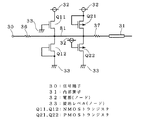
図1にこの発明の実施の形態1の第1の態様である入出力保護回路の構成を示す回路図である。同図に示すように、信号端子30は保護抵抗36の一端に接続され、保護抵抗36の他端は信号線(信号ノード)81を介して内部抵抗37の一端に接続され、内部抵抗37の他端は内部素子31に接続される。
【0052】
また、電源32,接地レベル33間にNMOSトランジスタQ11及びQ12が直列に接続されるともに、PMOSトランジスタQ21及びQ22が直列に接続される。NMOSトランジスタQ11はゲートが接地レベル33に接続され、ドレインが電源32に接続され、ソースが保護抵抗36の他端(内部抵抗37の一端)に接続される。NMOSトランジスタQ12のゲート及びソースは接地レベル33に接続され、ドレインはNMOSトランジスタQ11のソースに接続される。PMOSトランジスタQ21のゲート及びソースは電源32に接続され、ドレインは保護抵抗36の他端に接続され、PMOSトランジスタQ22のゲートは電源32に接続され、ソースは保護抵抗36の他端に接続され、ドレインは接地レベル33に接続される。なお、NMOSトランジスタQ11,Q12及びPMOSトランジスタQ21,Q22を、図23や図26に示すように複数のMOSトランジスタの並列接続で構成してもよい。
【0053】
このような構成において、正のサージ電圧が信号端子30に印加された場合は、電源電圧にPMOSトランジスタQ21及びQ22の閾値電圧を加えた電圧を上回る電圧が信号端子30に印加されることになり、信号端子30に対して順方向バイアス状態となるPMOSトランジスタQ21及びQ22を介して、サージ電圧を電源32及び接地レベル33にそれぞれ放電することができる。
【0054】
一方、負のサージ電圧が信号端子30に印加された場合は、接地レベルにNMOSトランジスタQ11及びQ12の閾値電圧を差し引いた電圧を下回る電圧が信号端子30に印加されることになり、信号端子30に対して順方向バイアス状態となるNMOSトランジスタQ11及びQ12を介して、サージ電圧を電源32及び接地レベル33に放電することができる。
【0055】
また、通常の動作時には、信号端子30に印加される動作信号は主として接地レベル〜電源レベルの電圧であるため、NMOSトランジスタQ11,Q12及びPMOSトランジスタQ21,Q22は全て逆方向バイアスされてオフ状態となり、動作信号はMOSトランジスタQ11,Q12,Q21あるいはQ22を介して電源32あるいは接地レベル33に漏れることなく、保護抵抗36及び内部抵抗37を経由して内部素子31に伝達される。特に、動作信号の電圧が接地レベル〜電源レベルの電圧に制限されている場合にはNMOSトランジスタQ11,Q12及びPMOSトランジスタQ21,Q22は確実にオフ状態となる。
【0056】
このように、実施の形態1の第1の態様の入出力保護回路は、正のサージ電圧、負のサージ電圧が印加されても、NMOSトランジスタQ11及びQ12並びにPMOSトランジスタQ21及びQ22のうち一方が、必ずサージ電圧に対して順方向バイアス状態となるため、ESD耐性良い入出力保護回路が得られる。
【0057】
また、NMOSトランジスタQ11,Q12及びPMOSトランジスタQ21,Q22は信号端子30に動作信号が入力された場合は逆方向バイアス状態となるように接続されているため、通常の動作時には影響を与えない。
【0058】
この入出力保護回路ではPチャネルおよびNチャネルのMOSトランジスタを2個ずつ用いている。通常、内部素子31として、図33に示すように、PMOSトランジスタ及びNMOSトランジスタからなるCMOSインバータを形成することが多く、2つのCMOSインバータの構成を少し変更するだけで、実施の形態1の第1の態様の入出力保護回路を簡単に製造することができる。
【0059】
<第2の態様の構成及び動作>
なお、第2の態様として、図2に示すように、NMOSトランジスタQ12及びPMOSトランジスタQ21をダイオードD11及びD12に置き換え、ダイオードD11のカソードを保護抵抗36の他端に接続するとともにアノードを接地レベル33に接続し、ダイオードD12のアノードを信号線81に接続するとともにカソードを電源32に接続するように構成してもよい。
【0060】
第2の態様において、正のサージ電圧が信号端子30に印加された場合には、信号端子30に対して順方向バイアス状態のダイオードD12及びPMOSトランジスタQ22を介して、サージ電圧を電源32及び接地レベル33にそれぞれ放電することができる。
【0061】
一方、負のサージ電圧が信号端子30に印加された場合には、信号端子30に対して順方向バイアス状態のNMOSトランジスタQ11及びダイオードD11を介して、サージ電圧を電源32及び接地レベル33にそれぞれ放電することができる。
【0062】
このように、実施の形態1の第2の態様の入出力保護回路は、正あるいは負のサージ電圧が印加された場合、NMOSトランジスタQ11及びダイオードD11並びにダイオードD12及びPMOSトランジスタQ22のうち一方が、必ずサージ電圧に対して順方向バイアス状態となるため、ESD耐性良い入出力保護回路が得られる。
【0063】
また、NMOSトランジスタQ11、ダイオードD11,D12及びPMOSトランジスタQ22は信号端子30に動作信号が入力された場合は常にオフ状態となるように接続されているため、通常の動作時には影響を与えない。
【0064】
さらに、第2の態様は、導電型式のMOSトランジスタを1個ずつバランス良く用いているため、第1の態様と同様、比較的簡単に製造することができる。
【0065】
<<実施の形態2>>
<原理>
図3はトランジスタの逆方向バイアスのゲートカップリング構造を示す回路図である。同図に示すように、入力信号IN(サージ電圧SV)に対し逆方向バイアス接続されたNMOSトランジスタQ3のゲートはキャパシタC1を介して入力信号INを受け、キャパシタC2を介して接地レベル33に接続される。すなわち、NMOSトランジスタQ3のゲートをキャパシタC1,C2によって電気的にフローティング状態にした構造がゲートカップリング構造である。このようなゲートカップリング構造はESD耐性を向上させる一つの手法として、例えばIEEE IRPS 1992 p・141に報告されている。
【0066】
このようなゲートカップリング構造では、入力信号INが通常の動作電圧の場合、キャパシタC1,C2のカップリングによりNMOSトランジスタQ3のゲート電位上昇が低く抑えられるため、NMOSトランジスタQ3はオフ状態となる。
【0067】
一方、正のサージ電圧SVの印加時などの場合は、NMOSトランジスタQ3のゲート電位が上昇し電流を流すため順方向バイアス接続された状態に近づけることが可能となる。このため、図4の放電特性のグラフに示すように、降伏誘起電圧を熱破壊電圧をよりも低く設定することが可能になり、順方向バイアス時に見られたように、図3で示したゲートカップリング構造のNMOSトランジスタQ3を入力信号IN,接地レベル33間に複数個並列接続した場合においても均一に電流を流すことが可能になり、ESD耐性を向上させることができる。このようなゲートカップリング構造をSOI基板上に効率的に形成したのが実施の形態2である。
【0068】
<第1の態様の構成及び動作>
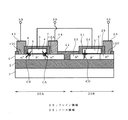
図5はこの発明の実施の形態2の第1の態様である入出力保護回路の構造を示す断面図である。同図に示すように、シリコン基板1上には絶縁層である埋め込み酸化膜2を挟んでSOI層であるシリコン薄膜3が設けられる。シリコン薄膜3は層間絶縁膜11によって2つの島20A,20Bに分離されている。島20Aにおいて、1017/cm3程度のp型の不純物が導入されたチャネル形成領域6、チャネル形成領域6を挟んで1020/cm3程度のn型の不純物が導入されたドレイン領域7及びソース領域8が形成される。一方、島20Bにおいて、1015〜1017/cm3程度のp型の不純物が導入されたp型拡散領域21、p型拡散領域21を挟んで1020/cm3程度のp型の不純物が導入されたp型拡散領域22,23が設けられる。
【0069】
さらに、島20Aのシリコン薄膜3のチャネル形成領域6並びにドレイン領域7及びソース領域8の一部上にはゲート酸化膜4を挟んでゲート電極5が形成される。一方、島20Bのシリコン薄膜3のp型拡散領域21及びp型拡散領域22,23の一部上にはゲート酸化膜4′を挟んでゲート電極5′が形成される。
【0070】
さらに、層間絶縁膜11が島20A,20Bを分離するとともにシリコン薄膜3上全面に形成され、ドレイン領域7の一部、ソース領域8の一部及びp型拡散領域22の一部上の層間絶縁膜11にコンタクトホール12A,12C及び12Eが設けられ、コンタクトホール12Aを介してドレイン領域7に電気的に接続されたアルミ配線14が設けられ、コンタクトホール12Cを介してソース領域8に電気的に接続されたアルミ配線13が設けられ、コンタクトホール12Eを介してp型拡散領域22に電気的に接続されたアルミ配線28が設けられる。そして、アルミ配線13は接地レベル33に接続され、アルミ配線14は入力端子50に接続され、アルミ配線28は接地レベル33に接続される。なお、入力端子50は図34のように保護抵抗を介して入力信号INを受ける構成でも、直接入力信号INを受ける構成であってもよい。
【0071】
したがって、島20Aにはゲート酸化膜4、ゲート電極5、チャネル形成領域6、ドレイン領域7及びソース領域8によってNMOSトランジスタQ3が形成されるとともに、ゲート酸化膜4を挟んで平面的に重複したゲート電極5の一部とドレイン領域7の一部とによって(ゲートオーバーラップ)キャパシタCA、ゲート酸化膜4を挟んで平面的に重複したゲート電極5の一部とソース領域8の一部とによって(ゲートオーバーラップ)キャパシタCBが形成される。
【0072】
一方、島20Bにはゲート酸化膜4′、ゲート電極5′、p型拡散領域21〜23によってNMOSトランジスタQ3と構造が類似した疑似MOSトランジスタ構造が得られる。そして、ゲート酸化膜4′を挟んで平面的に従属したゲート電極5′とp型拡散領域21及びp型拡散領域22,23の一部とによってキャパシタCCが形成される。そして、キャパシタCAは図3のキャパシタC1に相当し、キャパシタCB及びキャパシタCCの合成容量がキャパシタC2に相当する。
【0073】
このように、実施の形態2の第1の態様の入出力保護回路はSOI基板上にゲートカップリング構造のMOSトランジスタを形成している。このような構成において、入力端子50からの入力信号IN印加時には、キャパシタCAによってフローティング領域の電位が上昇する。ここでキャパシタCA基準電位である接地レベル33,ゲート電極5間に接続されたキャパシタCB及びCCの合成容量に比較して小さいため、NMOSトランジスタQ3のドレイン電位に比べ大きく低減されたゲート電位が付与されることになる。したがって、入力信号INが動作電圧(通常、接地レベル〜電源レベル及びその近傍領域の電圧となる)である場合はそのゲート電位はNMOSトランジスタQ3の閾値電圧を下回りNMOSトランジスタQ3がオフ状態となる。一方、入力信号INが正の高電圧の場合はゲート電位がNMOSトランジスタQ3の閾値電圧以上の上昇するとによりNMOSトランジスタQ3がオン状態となる。すなわち、NMOSトランジスタQ3は入力信号INに対して順方向バイアス接続状態となる。
【0074】
このように、実施の形態2の第1の態様の入出力保護回路は、効果的に降伏誘起電圧を低下させ、ESD耐性を向上させることができる。
【0075】
<第2の態様の構成及び動作>
図6はこの発明の実施の形態2の第2の態様である入出力保護回路の構造を示す断面図である。同図に示すように、シリコン基板1上には絶縁層である埋め込み酸化膜2を挟んでSOI層であるシリコン薄膜3が設けられる。シリコン薄膜3は層間絶縁膜11によって2つの島20A,20Bに分離されている。島20Aの構成は図5で示した第1の態様と同様である。
【0076】
島20Bにおいて、1016/cm3程度のp型の不純物が導入されたチャネル形成領域24、チャネル形成領域24を挟んで1020/cm3程度のp型の不純物が導入されたドレイン領域25,ソース領域26が設けられる。さらに、島20Bのシリコン薄膜3のチャネル形成領域24並びにドレイン領域25及びソース領域26の一部上にはゲート酸化膜4′を挟んでゲート電極5′が形成される。
【0077】
さらに、層間絶縁膜11が島20A,20Bを分離するとともにシリコン薄膜3上全面に形成され、ドレイン領域7の一部、ソース領域8の一部及びソース領域26の一部上の層間絶縁膜11にコンタクトホール12A,12C及び12Fが設けられ、コンタクトホール12Aを介してドレイン領域7に電気的に接続されたアルミ配線14が設けられ、コンタクトホール12Cを介してソース領域8に電気的に接続されたアルミ配線13が設けられ、コンタクトホール12Fを介してソース領域26に電気的に接続されたアルミ配線29が設けられる。そして、アルミ配線13は接地レベル33に接続され、アルミ配線14は入力端子50に接続され、アルミ配線29は接地レベル33に接続される。
【0078】
したがって、島20Aにはゲート酸化膜4、ゲート電極5、チャネル形成領域6、ドレイン領域7及びソース領域8によってNMOSトランジスタQ3が形成されるとともに、ゲート酸化膜4を挟んだゲート電極5の一部とドレイン領域7の一部とによってキャパシタCA、ゲート酸化膜4を挟んだゲート電極5の一部とソース領域8の一部とによってキャパシタCBが形成される。
【0079】
一方、島20Bにはゲート酸化膜4′、ゲート電極5′、p型拡散領域21,25及び26によってNMOSトランジスタQ3と構造が類似した疑似NMOSトランジスタ構造が得られる。そして、ゲート酸化膜4′を挟んだゲート電極5′とドレイン領域25とソース領域26の一部とによってキャパシタCDが形成される。そして、キャパシタCAは図3のキャパシタC1に相当し、キャパシタCB及びキャパシタCDの合成容量がキャパシタC2に相当する。
【0080】
ただし、キャパシタCDはチャネル形成領域24が反転する程度の電圧がゲート電極5′に与えられたときはじめて機能する。チャネル形成領域24は1016/cm3程度と低いため、比較的低い電圧がゲート電極5′に与えられてもチャネル形成領域24は反転する。
【0081】
このように、実施の形態2の第2の態様の入出力保護回路はSOI基板上にゲートカップリング構造のMOSトランジスタを形成することにより、第1の態様と同様、入力信号INが動作信号の場合は逆方向バイアス接続状態となり、入力信号INが正の高電圧の場合は順方向バイアス接続状態となり、第1の態様と同様の効果を奏する。
【0082】
<第3の態様の構成及び動作>
図7はこの発明の実施の形態2の第3の態様である入出力保護回路の構造を示す断面図である。同図に示すように、シリコン基板1上には絶縁層である埋め込み酸化膜2を挟んでシリコン薄膜3が設けられる。シリコン薄膜3は層間絶縁膜11によって2つの島20A,20Bに分離されている。島20Aの構成は図5で示した第1の態様と同様である。
【0083】
島20Bにおいて、1015〜1017/cm3程度のp型の不純物が導入されたp型拡散領域52,54、チャネル形成領域52を挟んで1020/cm3程度のp型の不純物及びn型の不純物がそれぞれ導入されたp型拡散領域51及びn型拡散領域53、p型拡散領域54を挟んで1020/cm3程度のn型の不純物及びp型の不純物がそれぞれ導入されたn型拡散領域53及びp型拡散領域55が形成される。したがって、n型拡散領域53はp型拡散領域52,54間に形成される。さらに、島20Bのシリコン薄膜3のp型拡散領域52及びp型拡散領域54上にはゲート酸化膜43及び44を挟んでゲート電極16及び17が形成される。
【0084】
さらに、層間絶縁膜11が島20A,20Bを分離するとともにシリコン薄膜3上全面に形成され、ドレイン領域7の一部、ソース領域8の一部、p型拡散領域51の一部、n型拡散領域53の一部及びp型拡散領域55の一部上の層間絶縁膜11にコンタクトホール12A,12C、12G、12H及び12Iが設けられ、コンタクトホール12Aを介してドレイン領域7に電気的に接続されたアルミ配線14が設けられ、コンタクトホール12Cを介してソース領域8に電気的に接続されたアルミ配線13が設けられ、コンタクトホール12Gを介してp型拡散領域51に電気的に接続されたアルミ配線15Aが設けられ、コンタクトホール12Hを介してn型拡散領域53に電気的に接続されたアルミ配線15Bが設けられ、コンタクトホール12Iを介してp型拡散領域55に電気的に接続されたアルミ配線15Cが設けられる。そして、アルミ配線13は接地レベル33に接続され、アルミ配線14は入力端子50に接続され、アルミ配線15A及び15Cは接地レベル33に接続され、アルミ配線15Bは島20Aのゲート電極5に接続される。
【0085】
したがって、島20Aには、第1及び第2の態様と同様に、ゲート酸化膜4、ゲート電極5、チャネル形成領域6、ドレイン領域7及びソース領域8によってNMOSトランジスタQ3が形成されるとともに、ゲート酸化膜4を挟んだゲート電極5の一部とドレイン領域7の一部とによってキャパシタCAに相当するキャパシタ、ゲート酸化膜4を挟んだゲート電極5の一部とソース領域8の一部とによってキャパシタCBに相当するキャパシタが形成される。
【0086】
一方、島20Bにはゲート酸化膜43、ゲート電極16、p型拡散領域51,52及びn型拡散領域53によってNMOSトランジスタQ3と構造が類似した第1の疑似MOSトランジスタ構造が得られ、ゲート酸化膜44、ゲート電極17、p型拡散領域54,55及びn型拡散領域53によってNMOSトランジスタQ3と構造が類似した第2の疑似MOSトランジスタ構造が得られる。
【0087】
そして、島20Bにはp型拡散領域52とn型拡散領域53及びn型拡散領域53とp型拡散領域54との接合容量の合成容量であるキャパシタCE(図示せず)が形成される。そして、キャパシタCAは図3のキャパシタC1に相当し、キャパシタCB及びキャパシタCEの合成容量がキャパシタC2に相当する。
【0088】
このように、実施の形態2の第3の態様の入出力保護回路はSOI基板上にゲートカップリング構造のMOSトランジスタを形成することにより、第1及び第2の態様と同様、入力信号INが動作信号の場合に逆方向バイアス接続状態となり、入力信号INが正の高電圧の場合に順方向バイアス接続状態となり、第1の態様と同様の効果を奏する。
【0089】
さらに第3の態様は以下の効果も奏する。第1及び第2の態様のようにMOSトランジスタQ3のゲート電極5がフローティング状態の場合、初期電圧が不安定になる欠点がある。しかしながら、第3の態様ではゲート電極5,接地レベル33間に接合容量からなるキャパシタCEを用いているため、接合を流れる微少電流により、基準電位である接地レベル33にNMOSトランジスタQ3のゲート電極5を固定することができる。したがって、第3の態様では、通常動作時には、初期電圧が不安定になることなくNMOSトランジスタQ3のゲート電極5を接地レベルに固定し、サージ電圧印加時のみにゲート電位を効率的に持ち上げることができる効果を奏する。
【0090】
<<実施の形態3>>
<原理>
MOSトランジスタのESD耐性を向上させるにはパンチスルーが起きやすい構造にしてパンチスルー電圧を降伏誘起電圧より低下させる方法がある。このような構造のMOSトランジスタを図20に示すように入力端子に対し逆バイアス接続した場合、サージが印加時に低く設定されたパンチスルー電圧に達するとMOSトランジスタはパンチスルー現象によって早期に降伏し、図30で示したダイオードの順方向接続の放電現象と同様な放電現象を起こすようになるため、EDS耐性が向上する。
【0091】
しかしながら、パンチスルー電圧を低下させるのはMOSトランジスタの動作特性を劣化させるため実動作上は望ましくない。以上の技術的背景を考慮したのが実施の形態3である。
【0092】
<第1の態様の構成及び動作>
図8はこの発明の実施の形態3の第1の態様である半導体装置の入出力保護回路部と内部回路部とにそれぞれ形成されるSOI基板上のMOSトランジスタ構造を示す断面図である。同図に示すように、シリコン基板1上には絶縁層である埋め込み酸化膜2を挟んでSOI層であるシリコン薄膜3が設けられる。シリコン薄膜3は層間絶縁膜11等によって入出力保護回路部45、内部回路部46に分離されている。入出力保護回路部45において、1016/cm3のp型の不純物が導入されたチャネル形成領域6A、チャネル形成領域6Aを挟んで1020/cm3程度のn型の不純物が導入されたドレイン領域7及びソース領域8が形成される。一方、内部回路部46において、1017/cm3程度のp型の不純物が導入されたチャネル形成領域6′、チャネル形成領域6′を挟んで1020/cm3程度のn型の不純物が導入されたドレイン領域7′及びソース領域8′が設けられる。
【0093】
さらに、入出力保護回路部45のシリコン薄膜3のチャネル形成領域6A並びにドレイン領域7及びソース領域8の一部上にはゲート酸化膜4を挟んでゲート電極5pが形成される。一方、内部回路部46のシリコン薄膜3のチャネル形成領域6′並びにドレイン領域7′及びソース領域8′の一部上にはゲート酸化膜4′を挟んでゲート電極5nが形成される。ただし、ゲート電極5pはp型のポリシリコンを用いて形成され、ゲート電極5nはn型のポリシリコンを用いて形成される。
【0094】
さらに、層間絶縁膜11が入出力保護回路部45,内部回路部46を分離するとともにシリコン薄膜3上全面に形成され、ドレイン領域7,7′の一部、ソース領域8,8′の一部上の層間絶縁膜11にコンタクトホール12A,12A′、12B,12B′がそれぞれ設けられ、コンタクトホール12A,12A′を介してドレイン領域7,7′に電気的に接続されたアルミ配線14,14′がそれぞれ設けられ、コンタクトホール12B,12B′を介してソース領域8,8′に電気的に接続されたアルミ配線13,13′がそれぞれ設けられる。
【0095】
したがって、入出力保護回路部45にはゲート電極5p、チャネル形成領域6A、ドレイン領域7及びソース領域8によってNMOSトランジスタ(入出力保護用NMOSトランジスタ)が形成され、内部回路部46にはゲート電極5n、チャネル形成領域6′、ドレイン領域7′及びソース領域8′によってNMOSトランジスタ(内部回路用NMOSトランジスタ)が形成される。
【0096】
チャネル形成領域6Aはチャネル形成領域6′より不純物濃度が低く設定されているためパンチスルー電圧が低くなる。一方、チャネル形成領域6Aの不純物濃度が低いとその閾値電圧が低くなる性質があり、これを補うべくゲート電極5pをn型のポリシリコンを用いるよりも閾値が高くなる性質を有するp型のポリシリコンを用いる。そして、チャネル形成領域6Aの不純物濃度とゲート電極5nの不純物濃度を調整することにより、内部回路部46に形成されるNMOSトランジスタと同程度の閾値電圧に設定することができる。
【0097】
このように、実施の形態4の第1の態様の入出力保護回路部45に形成されるNMOSトランジスタは、内部回路部46に形成されるNMOSトランジスタと同程度の閾値電圧を維持しながら、パンチスルー電圧を下げているため、ESD耐性の高い入出力保護回路を得ることができる。また、内部回路部46に形成されるNMOSトランジスタはパンチスルー電圧を下げていないため、パンチスルー電圧低下による動作特性の劣化はない。
【0098】
<第2の態様の構成及び動作>
図9はこの発明の実施の形態4の第2の態様である半導体装置の入出力保護回路部と内部回路部とにそれぞれ形成されるSOI基板上のMOSトランジスタ構造を示す断面図である。同図に示すように、シリコン基板1上には絶縁層である埋め込み酸化膜2を挟んでSOI層であるシリコン薄膜3が設けられる。シリコン薄膜3は層間絶縁膜11等によって入出力保護回路部45、内部回路部46に分離されている。入出力保護回路部45において、1017/cm3程度のn型の不純物が導入されたチャネル形成領域6n、チャネル形成領域6nを挟んで1020/cm3程度のn型の不純物が導入されたドレイン領域7及びソース領域8が形成される。
【0099】
さらに、入出力保護回路部45のシリコン薄膜3のチャネル形成領域6n並びにドレイン領域7及びソース領域8の一部上にはゲート酸化膜4を挟んでp型のポリシリコンからなるゲート電極5pが形成される。なお、上記以外の構成は図8で示した第1の態様と同様である。
【0100】
したがって、入出力保護回路部45にはゲート電極5p、チャネル形成領域6n、ドレイン領域7及びソース領域8によってNMOSトランジスタが形成され、内部回路部46にはゲート電極5n、チャネル形成領域6′、ドレイン領域7′及びソース領域8′によってNMOSトランジスタが形成される。
【0101】
入出力保護回路部45に形成されるNMOSトランジスタのチャネル形成領域6nはドレイン領域7及びソース領域8と同じ導電型のアキュミュレーションモードで形成されるためパンチスルー電圧が低くなる。一方、アキュミュレーションモードの場合はその閾値電圧が低くなる性質があるため、第1の態様と同様、これを補うべくゲート電極5nをn型のポリシリコンを用いるよりも閾値が高くなる性質を有するp型のポリシリコンを用いることにより、内部回路部46に形成されるNMOSトランジスタと同程度の閾値電圧に設定している。したがって、入出力保護回路部45のNMOSトランジスタを逆バイアス接続した場合に、そのゲート電位が多少上昇しても誤ってオン状態となることはない。
【0102】
このように、実施の形態4の第2の態様の入出力保護回路部45に形成されるNMOSトランジスタは、内部回路部46に形成されるNMOSトランジスタと同程度の閾値電圧を維持しながら、パンチスルー電圧を下げているため、ESD耐性の高い入出力保護回路を得ることができる。また、内部回路部46に形成されるNMOSトランジスタはパンチスルー電圧を下げていないため、パンチスルー電圧低下による動作特性の劣化はない。
【0103】
<その他>
なお、実施の形態3の第1及び第2の態様はNMOSトランジスタを例にして説明したが、各構成要素の導電型を逆にすることによってPMOSトランジスタにも適用可能であることは勿論である。
【0104】
また、第1及び第2の態様では、入出力保護回路部45のNMOSトランジスタのゲート電極5pの導電型をp型にしたが、内部回路部46のNMOSトランジスタのゲート電極5nと同様にn型に構成しても、閾値電圧は低下するもののパンチスルー電圧の低下によるESD耐性の向上を図ることはできる。
【0105】
さらに、図1あるいは図2で示した実施の形態1のNMOSトランジスタQ11,Q12及びPMOSトランジスタQ21,Q22として、実施の形態3の第1あるいは第2の態様の構造のMOSトランジスタを用いることにより、より一層ESD耐性の向上を図ることができる。
【0106】
<<実施の形態4>>
<原理>
SOI基板上にMOSトランジスタと共にダイオードを形成する場合、MOSトランジスタの製造プロセスを利用して、図36で示したような上部にゲート酸化膜4,4′及びゲート電極5,5′が形成されるダイオードが用いられるのが一般的である。
【0107】
しかしながら、ゲート酸化膜4,4′は破壊されやすく、ゲート酸化膜4,4′の存在はESD耐性を劣化させる要因となっている。そこで、SOI基板上にゲート酸化膜及びゲート電極が形成されないダイオードを用いて入出力保護回路を構成したのが実施の形態4である。
【0108】
<構成及び動作>
図10及び図11はこの発明の実施の形態4である半導体装置に用いられる入出力保護回路の構成を示す断面図及び平面図である。なお、図11のBB断面が図10となる。また、図10及び図11で示されるダイオードは例えば図32のダイオード38,39、図2のダイオードD11,D12に相当する。
【0109】
図10及び図11に示すように、シリコン基板1上には絶縁層である埋め込み酸化膜2を挟んでシリコン薄膜3が設けられる。シリコン薄膜3は層間絶縁膜11によって2つの島19A,19Bに分離されており、1017/cm3程度のp型の不純物が導入されたアノード領域9B、1017/cm3程度のn型の不純物が導入されたカソード領域10Bがそれぞれ設けられ、アノード領域9Bを挟んでアノード領域9A及びカソード領域10Aが設けられ、カソード領域10Bを挟んでアノード領域9C及びカソード領域10Cが設けられる。なお、アノード領域9A及びアノード領域9Cには1020/cm3程度のp型の不純物が導入され、カソード領域10A及びカソード領域10Cには1020/cm3程度のn型の不純物が導入される。したがって、アノード領域9A,9B及びカソード領域10Aによってダイオード39が構成され、アノード領域9C、カソード領域10B及び10Cによってダイオード38が構成される。
【0110】
そして、カソード領域10A、アノード領域9C、アノード領域9A及びカソード領域10Cそれぞれの表面にシリサイド領域27A〜27Dが選択的に形成される。
【0111】
シリサイド領域27A〜27Dはアノード領域9A〜9C及びカソード領域10A〜10C形成後に絶縁膜を堆積し、アノード領域9A,9C及びカソード領域10A,10C一部を開口して開口部分に自己整合的に形成してもよい。あるいは内部回路部46のシリサイド形成時には入出力保護回路部45の全面を絶縁膜で覆うことによりシリサイド領域は形成せず、コンタクトホールの形成工程でコンタクトホール12A〜12Dを設けた後、コンタクトホール12A〜12Dを介してカソード領域10A、アノード領域9C、アノード領域9A及びカソード領域10Cの表面に選択的にシリサイド領域を形成してもよい。
【0112】
さらに、層間絶縁膜11が島19A,19Bを分離するとともにシリコン薄膜3上全面に形成され、シリサイド領域27A〜27Dの一部上の層間絶縁膜11にコンタクトホール12A〜12Dが設けられ、コンタクトホール12A,12Bを介してシリサイド領域27A,27Bに電気的に接続されたアルミ配線14が設けられ、コンタクトホール12Cを介してシリサイド領域27Cに電気的に接続されたアルミ配線13が設けられ、コンタクトホール12Dを介してシリサイド領域27Dに電気的に接続されたアルミ配線15が設けられる。そして、アルミ配線13は接地レベル33に接続され、アルミ配線14は入力端子50に接続され、アルミ配線15は電源32に接続される。なお、入力端子50は図32の保護抵抗36の他端に接続されても、直接入力信号INを受ける構成であってもよい。また、図11において層間絶縁膜11は図示していない。
【0113】
このような構成の実施の形態4の入出力保護回路は、図32及び図36で示した従来の入出力保護回路と同様、正のサージ電圧が印加されると、ダイオード39のアノード領域9Bとカソード領域10Aとの間の接合が降伏し、接地レベル33にサージ電圧を放電する。同時にダイオード38が順方向バイアスされ、電源32にサージ電圧を放電する。また、サージ電圧として負の高電圧が印加される場合には逆にダイオード38のアノード領域9Cとカソード領域10Bとの間の接合が降伏し電源32にサージ電圧を放電するとともに、ダイオード39が順方向バイアスされて接地レベル33にサージ電圧を放電する。
【0114】
実施の形態4の入出力保護回路で用いられるダイオードは上部にESD耐性劣化の要因となるゲート酸化膜が形成されない分、図36で示した従来構造のダイオードを用いた場合よりも、良好なESD耐性を得ることができる。
【0115】
加えて、アノード領域9A,9C及びカソード領域10A,10Cとアルミ配線13〜15との接続をシリサイド領域27A〜27Dを用いて行うことにより、コンタクト抵抗の低減を図ることができる。
【0116】
<その他>
さらに、図2で示した実施の形態1の第2の態様のダイオードD11,D12として、実施の形態4の構造のMOSトランジスタを用いることにより、より一層ESD耐性の向上を図ることができる。
【0117】
<<実施の形態5>>
<原理>
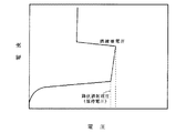
SOI基板上に形成されるMOSトランジスタ(上部にゲート電極を有するダイオード、キャパシタを含む)において、図12の平面図に示すように、ゲート電極5が、シリコン薄膜3の活性領域47(ドレイン領域7,ソース領域8を内部に有する)からはみ出した平面構造の場合、図12のC−C断面である図13に示すように、絶縁層2上に島状に形成された活性領域47(シリコン薄膜3)の端部を覆うようにゲート電極5を形成することになる。
【0118】
活性領域47の端部は活性領域47のパターニング時に受けたエッチングダメージによって結晶品質は悪いため活性領域47の端部近傍領域に形成されるゲート酸化膜4の品質は元々悪い。そこに、活性領域47の端部を覆ってゲート電極5を形成すると、ゲート電極5の材料形成時に活性領域47の端部により大きなストレスが発生するため、活性領域47の端部のゲート酸化膜4の品質はさらに悪化してしまい、その結果、ESD耐性を劣化を招いてしまう。
【0119】
そこで、SOI基板上にシリコン薄膜3の活性領域からはみ出さない平面構造のゲート電極を有するMOSトランジスタを用いて入出力保護回路を構成したのが実施の形態5である。
【0120】
<第1の態様>
図14はこの発明の実施の形態5の半導体装置の入出力保護回路に用いられるMOSトランジスタの第1の態様の平面構造を示す平面図である。同図に示すように、ゲート電極5を内部に2つの開口部を有する「日」の字状に形成し、2つの開口部分にドレイン領域7、ソース領域8を形成している。そして、コンタクトホール12Aを介してドレイン領域7と電気的に接続したアルミ配線14を形成し、コンタクトホール12Cを介してソース領域8と電気的に接続したアルミ配線13を形成し、コンタクトホール68を介してゲート電極5と電気的に接続したアルミ配線58を形成している。なお、図14で示した平面構造は、例えば図5で示した実施の形態2の第1の態様において島20Aに形成されるNMOSトランジスタに適用することができる。
【0121】
このように、実施の形態5の第1の態様は、平面上においてゲート電極5が活性領域47内に形成されているため、活性領域47の端部にゲート電極5が形成されることがない分、ESD耐性の向上を図ることができる。
【0122】
<第2の態様>
図15はこの発明の実施の形態5の半導体装置の入出力保護回路に用いられるMOSトランジスタの第2の態様の平面構造を示す平面図である。同図に示すように、ゲート電極17を内部に2つの開口部を有する「日」の字状に形成し、2つの開口部分にn型拡散領域53、p型拡散領域55を形成している。そして、コンタクトホール12Hを介してn型拡散領域53と電気的に接続したアルミ配線15Bを形成し、コンタクトホール12Iを介してp型拡散領域55と電気的に接続したアルミ配線15Cを形成している。なお、図15で示した平面構造は、例えば図7で示した実施の形態2の第3の態様において島20Bに形成されるゲート電極17がフローティング状態となったゲートカップリング構造のキャパシタに適用することができる。
【0123】
このように、実施の形態5の第2の態様は、平面上においてゲート電極17が活性領域47内に形成されているため、活性領域47の端部にゲート電極17が形成されることがない分、ESD耐性の向上を図ることができる。
【0124】
<第3の態様>
図16はこの発明の実施の形態5の半導体装置の入出力保護回路に用いられるMOSトランジスタの第3の態様の平面構造を示す平面図である。同図に示すように、ゲート電極5を内部に1つの開口部を囲む「口」の字状に形成し、その開口部分にドレイン領域7を形成し、ゲート電極5の外側にある活性領域47にソース領域8を形成している。そして、コンタクトホール12Aを介してドレイン領域7と電気的に接続したアルミ配線14を形成し、コンタクトホール12Cを介してソース領域8と電気的に接続したアルミ配線13を形成し、コンタクトホール68を介してゲート電極5と電気的に接続したアルミ配線58を形成している。なお、図16で示した平面構造は、例えば図5で示した実施の形態2の第1の態様において島20Aに形成されるNMOSトランジスタに適用することができる。
【0125】
このように、実施の形態5の第3の態様は、平面上においてゲート電極5が活性領域47内に形成されているため、活性領域47の端部にゲート電極5が形成されることがない分、ESD耐性の向上を図ることができる。
【0126】
<第4の態様>
図17はこの発明の実施の形態5の半導体装置の入出力保護回路に用いられるMOSトランジスタの第4の態様の平面構造を示す平面図である。同図に示すように、ゲート電極17を内部に1つの開口部を囲む「口」の字状に形成し、その開口部分にp型拡散領域55を形成し、ゲート電極17の外側にある活性領域47にn型拡散領域53を形成している。そして、コンタクトホール12Hを介してn型拡散領域53と電気的に接続したアルミ配線15Bを形成し、コンタクトホール12Iを介してp型拡散領域55と電気的に接続したアルミ配線15Cを形成している。なお、図17で示した平面構造は例えば、図7で示した実施の形態2の第3の態様において島20Bに形成されるゲート電極17がフローティング状態となったキャパシタに適用することができる。
【0127】
このように、実施の形態5の第4の態様は、平面上においてゲート電極17が活性領域47内に形成されているため、活性領域47の端部にゲート電極17が形成されることがない分、ESD耐性の向上を図ることができる。
【0128】
<その他>
また、図1あるいは図2で示した実施の形態1のNMOSトランジスタQ11,Q12及びPMOSトランジスタQ21,Q22として、実施の形態5の第1あるいは第3の態様の構造のMOSトランジスタを用いることにより、より一層ESD耐性の向上を図ることができる。
【0129】
<<補足>>
上記した実施の形態2〜実施の形態5の構成では、NMOSトランジスタを中心に説明したが、導電型式を逆にすることによってPMOSトランジスタに適用可能なのは勿論である。また、主に電源32側にPMOSトランジスタ,接地レベル33側にNMOSトランジスタを配置する構成を示したが、電源32及び接地レベル33のうち一方に入出力保護用MOSトランジスタを設ける構成でも同様の効果を有する。また、MOSトランジスタをダイオード接続して、電源32側にNMOSトランジスタ,接地33側にPMOSトランジスタを設けても同様の効果を奏する。
【0130】
さらに、MOSトランジスタ,ダイオードを各種組み合わせて接続して複雑な入出力保護回路を構成しても少なくとも上記した実施の形態と同様な効果が得られるのはいうまでもない。
【0131】
【発明の効果】
以上説明したように、この発明における請求項1記載の半導体装置の入出力保護回路は、各々が電源ノードあるいは基準電位ノードと信号端子との間に設けられ、信号端子に動作信号が印加されるときに逆方向バイアスとなり、第1あるいは第2の極性の電圧が印加されるときに順方向バイアスとなるPN接合部を有する第1〜第4の放電素子を有している。
【0132】
したがって、第1の極性を有するサージ電圧が信号端子より印加されるときは、順方向バイアス状態の第1及び第3の放電素子がそれぞれ電源ノード及び基準電位ノードにそのサージ高電圧を放電させ、第2の極性を有するサージ電圧が信号端子より印加されるときは、順方向バイアス状態の第2及び第4の放電素子がそれぞれ電源ノード及び基準電位ノードにそのサージ電圧を放電させることができる。
【0133】
その結果、どのようなサージ電圧に対しても必ず順方向バイアス状態で電源ノード及び基準電位ノードそれぞれに放電する2つの放電素子が存在するため、ESD耐性の良い入出力保護回路を得ることができる。
【0134】
また、第1〜第4の放電素子のPN接合部は、信号端子に動作信号が印加された場合にすべて逆方向バイアス状態となるため、動作信号が第1〜第4の放電素子を介して電源ノードあるいは接地線に漏れることはなく、入出力保護回路が内部回路の通常動作に悪影響を与えることもない。
【0135】
請求項2記載の半導体装置は、第1の導電型の第1及び第3のMOSトランジスタと、第2の導電型の第2及び第4のMOSトランジスタとによって入出力保護回路を構成することにより、異なる導電型式のトランジスタを2個ずつ用いているため、入出力保護回路を容易に製造することができる。
【0136】
請求項5記載の半導体装置は、1つの第1の導電型の第1のトランジスタと、1つの第2の導電型の第2のトランジスタと2つの第1及び第2のダイオードによって入出力保護回路を構成することにより、異なる導電型式のトランジスタを1個ずつ用いているため、入出力保護回路を容易に製造することができる。
【0137】
請求項7記載の半導体装置は、信号端子と信号ノードとの間に介挿される第1の内部抵抗と、信号ノードと内部回路との間に介挿される第2の内部抵抗とを有しているため、信号端子に第1あるいは第2の極性のサージ電圧が印加された場合に、第1の内部抵抗によってその伝播遅延を生じさせ、第2の内部抵抗により内部回路への伝播を妨げたりすることにより内部回路の保護を図ることができる。
【図面の簡単な説明】
【図1】 この発明の実施の形態1である半導体装置の入出力保護回路の構成を示す回路図である。
【図2】 この発明の実施の形態1である半導体装置の入出力保護回路の他の構成を示す回路図である。
【図3】 ゲートカップリング断面構造のNMOSトランジスタを示す回路図である。
【図4】 図3で示したNMOSトランジスタの放電特性を示すグラフである。
【図5】 この発明の実施の形態2である半導体装置の入出力保護回路の第1の態様の断面構造を示す断面図である。
【図6】 実施の形態2の第2の態様の断面構造を示す断面図である。
【図7】 実施の形態2の第3の態様の断面構造を示す断面図である。
【図8】 この発明の実施の形態3である半導体装置の入出力保護回路の第1の態様の断面構造を示す断面図である。
【図9】 実施の形態3の第2の態様の断面構造を示す断面図である。
【図10】 この発明の実施の形態4である半導体装置の入出力保護回路の断面構造を示す断面図である。
【図11】 図10で示した実施の形態4の平面構造を示す平面図である。
【図12】 実施の形態5の原理説明用の平面図である。
【図13】 実施の形態5の原理説明用の断面図である。
【図14】 この発明の実施の形態5である半導体装置の入出力保護回路の第1の態様の平面構造を示す平面図である。
【図15】 実施の形態5の第2の態様の平面構造を示す平面図である。
【図16】 実施の形態5の第3の態様の平面構造を示す平面図である。
【図17】 実施の形態5の第4の態様の平面構造を示す平面図である。
【図18】 SOI断面構造を示す断面図である。
【図19】 逆方向バイアス接続されたNMOSトランジスタの放電特性を示すグラフである。
【図20】 逆方向バイアス接続のNMOSトランジスタを示す回路図である。
【図21】 熱暴走破壊されたMOSトランジスタの平面構造を示す平面図である。
【図22】 入力,接地間に複数のNMOSトランジスタを並列に接続した平面構造を示す平面図である。
【図23】 図22の回路構成を示す回路図である。
【図24】 順方向バイアス接続のNMOSトランジスタを示す回路図である。
【図25】 順方向バイアス接続されたNMOSトランジスタの放電特性を示す説明図である。
【図26】 複数のNMOSトランジスタを用いて順方向バイアス接続を行う場合の構成を示す回路図である。
【図27】 逆方向バイアス接続のダイオードを示す回路図である。
【図28】 逆方向バイアス接続されたダイオードの放電特性を示すグラフである。
【図29】 順方向バイアス接続のダイオードを示す回路図である。
【図30】 順方向バイアス接続されたダイオードの放電特性を示すグラフである。
【図31】 従来の入出力保護回路の構成を示す回路図である。
【図32】 従来の入出力保護回路の構成を示す回路図である。
【図33】 内部素子の一例を示す回路図である。
【図34】 図31で示した入出力保護回路の一部の平面構造を示す平面図である。
【図35】 図31で示した入出力保護回路の一部の断面構造を示す断面図である。
【図36】 図32で示した入出力保護回路の一部の断面構造を示す断面図である。
【符号の説明】
5,5′,5n,5p,16,17 ゲート電極、6,6′,6A,6n チャネル形成領域、7,7′,25 ドレイン領域、8,8′,26 ソース領域、9A〜9C アノード領域、10A〜10C カソード領域、14 シリサイドプロテクト層、21〜23,51,52,54,55 p型拡散領域、53 n型拡散領域53、27A〜27D シリサイド領域、30 信号端子、31 内部素子、32 電源(ノード)、33 接地レベル(ノード)、45 入出力保護回路部、46 内部回路部、47 活性領域、D11,D12 ダイオード、Q11,Q12 NMOSトランジスタ、Q21,Q22 PMOSトランジスタ。[0001]
BACKGROUND OF THE INVENTION
The present invention relates to a semiconductor device in which a MOS transistor is formed on an SOI substrate, and particularly to its input / output protection function.
[0002]
[Prior art]
When forming a MOS device on a bulk silicon substrate, a surge can be discharged to the substrate through a PN junction, but in the case of an SOI (Silicon-on-insulator) device in which a MOS device is formed on an SOI layer on a buried insulating layer. In addition, there is no structural path for the surge to escape to the substrate due to the buried insulating layer. In particular, in a thin-film SOI structure in which the source region and drain region of a MOS transistor reach the buried oxide film, there is no vertical discharge path, and horizontal discharge is essential due to the structure. For this reason, it discharges to a power supply line or a ground line laterally through a MOS transistor or a diode.
[0003]
FIG. 31 is a circuit diagram showing a circuit configuration of an input / output protection circuit in a conventional SOI structure. As shown in the figure, first, one end of a resistor 36 (hereinafter referred to as a “protective resistor”) for limiting an inrush current is connected to the
[0004]
When a surge voltage is applied to the
[0005]
FIG. 32 shows an input formed in the same
[0006]
When a surge voltage is applied to the
[0007]
FIG. 33 shows an inverter circuit which is one of typical internal circuits. As shown in the figure, a PMOS transistor Q33 and an NMOS transistor Q34 are connected in series between a
[0008]
When the input / output protection circuit having the configuration shown in FIGS. 31 and 32 is connected to the input signal terminal 82 (input part of the internal circuit) with respect to the internal circuit shown in FIG. 33, the input circuit functions as an input protection circuit. When connected to the signal terminal 83 (the output portion of the internal circuit), it functions as an output protection circuit. Since the function and operation of the protection circuit are the same for both the input unit and the output unit, they will be described as “input / output protection circuit” below. However, a resistor is often not added when used as an output protection circuit.
[0009]
34 is a plan view showing a planar structure of the MOS type input / output protection circuit shown in FIG. 31, and FIG. 35 is a cross-sectional view taken along line AA of FIG. As shown in these drawings, a silicon
[0010]
Further, an
[0011]
As shown in FIG. 34, a
[0012]
Here, the gate electrode 5 'of the PMOS transistor Q31 is connected to the
[0013]
Next, the operation will be described with reference to FIG. 31, FIG. 34 and FIG. A surge due to static electricity enters from the
[0014]
36 is a cross-sectional view showing a cross-sectional structure of the diode-type input / output protection circuit shown in FIG. As shown in the figure, a silicon
[0015]
Further, an
[0016]
The structure of the diode part is the same as that shown in FIG. However, the
[0017]
Next, regarding the operation, the input / output protection circuit shown in FIG. 32 and FIG. 36 is the breakdown of the junction between the
[0018]
[Problems to be solved by the invention]
In the SOI structure, the thermal conductivity is poor due to the presence of the buried
[0019]
Furthermore, in the SOI structure, since the quality of the silicon
[0020]
The present invention has been made to solve the above-described problems, and an object of the present invention is to obtain an SOI structure semiconductor device with improved ESD resistance.
[0021]
[Means for Solving the Problems]
According to a first aspect of the present invention, there is provided a semiconductor device formed on an SOI substrate and corresponding to a signal node connected to each signal terminal, an internal circuit connected to the signal node, A power supply node connected to a power supply potential and a reference potential node connected to a reference potential, and the input / output protection circuit unit is provided between the power supply node and the signal node. , Each having a PN junction and the signal terminal, A potential between the power supply potential and the reference potentialWhen a first discharge element that is reverse biased when an operation signal is applied and forward biased when a surge voltage having a first polarity is applied and a surge voltage having a second polarity is applied Provided between the second discharge element serving as a forward bias, the signal node and the reference potential node, each having a PN junction and being connected to the signal terminalSaidWhen the operation signal is applied, a reverse bias is applied, and when a surge voltage having the first polarity is applied, a forward discharge is applied, and when a surge voltage having the second polarity is applied A fourth discharge element serving as a forward bias.
[0022]
3. The semiconductor device according to
4. The semiconductor device according to
5. The semiconductor device according to
[0023]
Claims5In the semiconductor device described above, the first discharge element is a first conductivity type MOS transistor, a control electrode thereof is connected to the reference potential node, and the second and third discharge elements are diodes, The fourth discharge element is a second conductivity type MOS transistor, and its control electrode is connected to the power supply potential node.
7. The semiconductor device according to
[0024]
And claims7The semiconductor device described includes a first internal resistor interposed between the signal terminal and the signal node, and a second internal resistor interposed between the signal node and the internal circuit. Yes.
[0035]
DETAILED DESCRIPTION OF THE INVENTION
<<
<Principle>
FIG. 18 is a cross-sectional view showing an SOI structure. As shown in the figure, a buried
[0036]
Such an SOI structure has a buried
[0037]
FIG. 19 is a graph showing the discharge characteristics of the NMOS transistor at the time of reverse bias connection. The graph of FIG. 19 shows the history of thermal runaway during reverse bias connection, such as when the input voltage IN (surge voltage SV) is applied to the drain of the NMOS transistor Q1 whose source and gate are grounded as shown in FIG. The thermal runaway process shown in FIG. 19 includes partial processes P1 to P5.
[0038]
When a positive surge voltage SV that is much higher than normal is applied to the drain of the NMOS transistor Q1 shown in FIG. 20, the drain voltage rapidly rises (P1). During the partial process P1, the NMOS transistor Q1 is reverse-biased, so that almost no current flows. When the breakdown induced voltage is reached, the NMOS transistor Q1 undergoes avalanche breakdown, causing a parasitic bipolar operation to drop to the holding voltage (P2). Thereafter, the voltage rises again due to the internal resistance of the NMOS transistor Q1 (P3), and when the thermal breakdown voltage is reached, the silicon portion forming a part of the NMOS transistor Q1 enters a molten state, and the resistance value between the source and the drain rapidly decreases. Therefore, the voltage decreases (P4). As a result, the positive feedback that the current flows concentratedly on the NMOS transistor Q1 whose resistance between the source and the drain is reduced works (P5), and the NMOS transistor Q1 is completely destroyed. For example, as shown in FIG. 21, a
[0039]
Normally, when an NMOS transistor is provided as an input / output protection circuit on an SOI substrate with a reverse bias, an NMOS transistor having a channel width W is connected in parallel between an input (voltage) IN and a ground level as shown in FIG. To be. In the example of FIG. 22, as shown in FIG. 23, six NMOS transistors T1 to T6 whose gates are grounded are provided in parallel between the input IN and the ground level. The NMOS transistor T1 includes a
[0040]
Thus, by providing six NMOS transistors T1 to T6 in parallel between the input IN and the ground level as input / output protection circuits on the SOI substrate, when current flows between the input IN and the ground level, six NMOS transistors The current is divided into transistors T1 to T6.
[0041]
However, when one of the NMOS transistors T1 to T6 reaches the avalanche breakdown voltage, the resistance between the source and drain of the transistor decreases, and current concentrates on the avalanche breakdown transistor. The breakdown voltage is not reached to prevent thermal breakdown.
[0042]
FIG. 25 is a graph showing the discharge characteristics of the NMOS transistor at the time of forward bias connection. The graph of FIG. 25 shows the history of thermal runaway during forward bias connection such as when the input voltage IN (surge voltage SV) is applied to the drain and gate of the NMOS transistor Q2 whose source is grounded as shown in FIG. ing.
[0043]
FIG. 25 is a graph showing discharge characteristics of the NMOS transistor at the time of forward bias connection shown in FIG. As shown in FIG. 25, when the forward bias is connected, the snapback phenomenon that the drain voltage decreases when the breakdown induced voltage is reached does not occur. Therefore, as shown in FIG. 26, the plurality of NMOS transistors T11 to T16 provided in parallel between the input IN and the ground level cause the avalanche breakdown almost uniformly with the application of the surge voltage SV, and the further surge voltage SV. When the thermal breakdown voltage is reached by the application of, a thermal runaway state occurs as in the case of reverse bias connection.
[0044]
When a plurality of NMOS transistors are connected in parallel as shown in FIG. 26, when some of the transistors avalanche breakdown, the drain voltage rises and other transistors also avalanche breakdown. As a result, all the transistors are avalanche breakdown, and since current flows uniformly to all the transistors, they are thermally destroyed at a thermal breakdown voltage higher than the breakdown induced voltage.
[0045]
In this way, when forward bias is connected, a phenomenon that current does not flow concentratedly to some of the avalanche breakdown transistors unlike when reverse bias is connected does not occur, so that relatively good ESD resistance can be obtained. it can.
[0046]
FIG. 28 is a graph showing the discharge characteristics of the diode at the time of reverse bias connection. The graph of FIG. 28 shows the history of thermal runaway during reverse bias connection such as when the surge voltage SV is applied to the cathode of the diode D1 whose anode is grounded as shown in FIG.
[0047]
Since the diode does not cause a parasitic bipolar operation, the voltage continues to rise even after avalanche breakdown, leading to thermal destruction. The fact that the thermal breakdown voltage is higher than the breakdown induced voltage is effective from the viewpoint of preventing current concentration as in the case of the NMOS transistor in the forward bias connection described above, but the breakdown induced voltage itself of the diode is high (MOS transistor). Therefore, the power consumption represented by the product of voltage and current increases (that is, heat increases), resulting in degradation of ESD resistance. However, when the junction breakdown voltage of the diode is reduced by high-concentration junction or the like, the breakdown induced voltage can be reduced, and the ESD resistance can be improved.
[0048]
FIG. 30 is a graph showing the discharge characteristics of the diode at the time of forward bias connection. The graph of FIG. 30 shows the history of thermal runaway during forward bias connection such as when the surge voltage SV is applied to the anode of the diode D1 whose cathode is grounded as shown in FIG.
[0049]
Since the forward connection of the diode can discharge a large current at a low voltage, a discharge characteristic desirable for ESD tolerance can be obtained. As shown in FIG. 30, avalanche breakdown occurs due to an increase in voltage, and when the thermal breakdown voltage is reached like other elements, the element is permanently destroyed due to thermal explosion.
[0050]
As described above, even when a transistor is used or a diode is used, current non-uniformity can be easily prevented and ESD resistance can be improved when the forward connection is used.
[0051]
<Configuration and operation of first aspect>
FIG. 1 is a circuit diagram showing a configuration of an input / output protection circuit according to a first mode of the first embodiment of the present invention. As shown in the figure, the
[0052]
Further, NMOS transistors Q11 and Q12 are connected in series between the
[0053]
In such a configuration, when a positive surge voltage is applied to the
[0054]
On the other hand, when a negative surge voltage is applied to the
[0055]
Further, during normal operation, the operation signal applied to the
[0056]
As described above, in the input / output protection circuit according to the first mode of the first embodiment, even when a positive surge voltage or a negative surge voltage is applied, one of the NMOS transistors Q11 and Q12 and the PMOS transistors Q21 and Q22 is Since it is always in the forward bias state with respect to the surge voltage, an input / output protection circuit with good ESD resistance can be obtained.
[0057]
Further, the NMOS transistors Q11 and Q12 and the PMOS transistors Q21 and Q22 are connected so as to be in a reverse bias state when an operation signal is input to the
[0058]
This input / output protection circuit uses two P-channel and two N-channel MOS transistors. Usually, as the
[0059]
<Configuration and Operation of Second Aspect>
As a second mode, as shown in FIG. 2, the NMOS transistor Q12 and the PMOS transistor Q21 are replaced with diodes D11 and D12, the cathode of the diode D11 is connected to the other end of the
[0060]
In the second embodiment, when a positive surge voltage is applied to the
[0061]
On the other hand, when a negative surge voltage is applied to the
[0062]
As described above, in the input / output protection circuit according to the second mode of the first embodiment, when a positive or negative surge voltage is applied, one of the NMOS transistor Q11, the diode D11, the diode D12, and the PMOS transistor Q22 is Since the forward bias state is always applied to the surge voltage, an input / output protection circuit with good ESD resistance can be obtained.
[0063]
Further, the NMOS transistor Q11, the diodes D11 and D12, and the PMOS transistor Q22 are connected so as to be always turned off when an operation signal is input to the
[0064]
Furthermore, since the second mode uses conductive MOS transistors one by one in a well-balanced manner, the second mode can be manufactured relatively easily as in the first mode.
[0065]
<<
<Principle>
FIG. 3 is a circuit diagram showing a reverse-biased gate coupling structure of a transistor. As shown in the figure, the gate of the NMOS transistor Q3 reversely biased with respect to the input signal IN (surge voltage SV) receives the input signal IN via the capacitor C1 and is connected to the
[0066]
In such a gate coupling structure, when the input signal IN is a normal operating voltage, the rise of the gate potential of the NMOS transistor Q3 is suppressed by the coupling of the capacitors C1 and C2, so that the NMOS transistor Q3 is turned off.
[0067]
On the other hand, when a positive surge voltage SV is applied, the gate potential of the NMOS transistor Q3 rises and a current flows, so that it can be brought close to a forward bias connection state. For this reason, as shown in the discharge characteristic graph of FIG. 4, the breakdown induced voltage can be set lower than the thermal breakdown voltage, and the gate shown in FIG. Even when a plurality of NMOS transistors Q3 having a coupling structure are connected in parallel between the input signal IN and the
[0068]
<Configuration and operation of first aspect>
FIG. 5 is a sectional view showing the structure of the input / output protection circuit according to the first mode of the second embodiment of the present invention. As shown in the figure, a silicon
[0069]
Further, a
[0070]
Furthermore, an
[0071]
Therefore, the NMOS transistor Q3 is formed on the
[0072]
On the other hand, a pseudo-MOS transistor structure similar in structure to the NMOS transistor Q3 is obtained on the
[0073]
As described above, the input / output protection circuit according to the first aspect of the second embodiment forms the MOS transistor having the gate coupling structure on the SOI substrate. In such a configuration, when the input signal IN is applied from the
[0074]
Thus, the input / output protection circuit according to the first aspect of the second embodiment can effectively reduce the breakdown induced voltage and improve the ESD resistance.
[0075]
<Configuration and Operation of Second Aspect>
FIG. 6 is a sectional view showing the structure of the input / output protection circuit according to the second mode of the second embodiment of the present invention. As shown in the figure, a silicon
[0076]
On
[0077]
Further, an
[0078]
Therefore, the island
[0079]
On the other hand, a pseudo-NMOS transistor structure similar to the NMOS transistor Q3 is obtained on the
[0080]
However, the capacitor CD functions only when a voltage sufficient to invert the channel formation region 24 is applied to the gate electrode 5 '. The channel forming region 24 is 1016/ CmThreeTherefore, the channel formation region 24 is inverted even when a relatively low voltage is applied to the gate electrode 5 '.
[0081]
As described above, the input / output protection circuit according to the second mode of the second embodiment forms the MOS signal having the gate coupling structure on the SOI substrate, so that the input signal IN is the operation signal as in the first mode. In this case, the reverse bias connection state is established. When the input signal IN is a positive high voltage, the forward bias connection state is established, and the same effect as that of the first aspect is obtained.
[0082]
<Configuration and Operation of Third Aspect>
FIG. 7 is a sectional view showing the structure of the input / output protection circuit according to the third mode of the second embodiment of the present invention. As shown in the figure, a silicon
[0083]
On
[0084]
Further, an
[0085]
Therefore, in the
[0086]
On the other hand, on the
[0087]
A capacitor CE (not shown) that is a combined capacitance of the junction capacitance of the p-
[0088]
As described above, the input / output protection circuit according to the third mode of the second embodiment forms the MOS transistor having the gate coupling structure on the SOI substrate, so that the input signal IN is the same as in the first and second modes. In the case of an operation signal, the reverse bias connection state is established, and when the input signal IN is a positive high voltage, the forward bias connection state is established, and effects similar to those of the first aspect are obtained.
[0089]
Furthermore, the third aspect also has the following effects. When the
[0090]
<<
<Principle>
In order to improve the ESD resistance of the MOS transistor, there is a method in which the punch-through voltage is made lower than the breakdown induced voltage by making the structure easy to cause punch-through. When the MOS transistor having such a structure is reverse-biased with respect to the input terminal as shown in FIG. 20, when the surge reaches a punch-through voltage set low during application, the MOS transistor breaks down early due to the punch-through phenomenon, Since the discharge phenomenon similar to the forward discharge phenomenon of the diode shown in FIG. 30 is caused, the EDS resistance is improved.
[0091]
However, lowering the punch-through voltage is undesirable in actual operation because it degrades the operating characteristics of the MOS transistor. The third embodiment takes the above technical background into consideration.
[0092]
<Configuration and operation of first aspect>
FIG. 8 shows an embodiment of the present invention.3FIG. 2 is a cross-sectional view showing a MOS transistor structure on an SOI substrate formed in an input / output protection circuit portion and an internal circuit portion of the semiconductor device according to the first embodiment of the present invention. As shown in the figure, a silicon
[0093]
Further, a gate electrode 5p is formed on the
[0094]
Further, the
[0095]
Therefore, an NMOS transistor (input / output protection NMOS transistor) is formed in the input / output
[0096]
Since the
[0097]
As described above, the NMOS transistor formed in the input / output
[0098]
<Configuration and Operation of Second Aspect>
FIG. 9 is a sectional view showing a MOS transistor structure on an SOI substrate formed in the input / output protection circuit portion and the internal circuit portion of the semiconductor device according to the second mode of the fourth embodiment of the present invention. As shown in the figure, a silicon
[0099]
Further, a gate electrode 5p made of p-type polysilicon is formed on the channel forming region 6n of the silicon
[0100]
Therefore, an NMOS transistor is formed in the input / output
[0101]
The channel formation region 6n of the NMOS transistor formed in the input / output
[0102]
As described above, the NMOS transistor formed in the input / output
[0103]
<Others>
Although the first and second modes of the third embodiment have been described by taking the NMOS transistor as an example, it is needless to say that it can also be applied to a PMOS transistor by reversing the conductivity type of each component. .
[0104]
In the first and second embodiments, the conductivity type of the gate electrode 5p of the NMOS transistor of the input / output
[0105]
Further, as the NMOS transistors Q11 and Q12 and the PMOS transistors Q21 and Q22 of the first embodiment shown in FIG. 1 or FIG. 2, by using the MOS transistor having the structure of the first or second aspect of the third embodiment, The ESD resistance can be further improved.
[0106]
<<
<Principle>
When forming a diode together with a MOS transistor on an SOI substrate,
[0107]
However, the
[0108]
<Configuration and operation>
10 and 11 are a sectional view and a plan view showing the configuration of the input / output protection circuit used in the semiconductor device according to the fourth embodiment of the present invention. In addition, the BB cross section of FIG. 11 becomes FIG. The diodes shown in FIGS. 10 and 11 correspond to, for example, the
[0109]
As shown in FIGS. 10 and 11, a silicon
[0110]
Silicide regions 27A to 27D are selectively formed on the surfaces of the
[0111]
The silicide regions 27A to 27D are formed in a self-aligned manner by depositing an insulating film after the
[0112]
Further, the
[0113]
The input / output protection circuit according to the fourth embodiment having such a configuration is similar to the conventional input / output protection circuit shown in FIGS. 32 and 36, when a positive surge voltage is applied, The junction with the
[0114]
Since the diode used in the input / output protection circuit of the fourth embodiment is not formed with a gate oxide film that causes deterioration of ESD resistance, the ESD is better than when the conventional diode shown in FIG. 36 is used. Resistance can be obtained.
[0115]
In addition,
[0116]
<Others>
Further, by using the MOS transistor having the structure of the fourth embodiment as the diodes D11 and D12 of the second mode of the first embodiment shown in FIG. 2, ESD resistance can be further improved.
[0117]
<<
<Principle>
In a MOS transistor (including a diode having a gate electrode on the upper part and a capacitor) formed on an SOI substrate, the
[0118]
Since the end portion of the
[0119]
In the fifth embodiment, therefore, an input / output protection circuit is configured using a MOS transistor having a gate electrode having a planar structure that does not protrude from the active region of the silicon
[0120]
<First aspect>
FIG. 14 is a plan view showing a planar structure of the first mode of the MOS transistor used in the input / output protection circuit of the semiconductor device according to the fifth embodiment of the present invention. As shown in the figure, the
[0121]
Thus, in the first mode of the fifth embodiment, since the
[0122]
<Second aspect>
FIG. 15 is a plan view showing a planar structure of a second mode of the MOS transistor used in the input / output protection circuit of the semiconductor device according to the fifth embodiment of the present invention. As shown in the figure, the
[0123]
Thus, in the second mode of the fifth embodiment, since the
[0124]
<Third Aspect>
FIG. 16 is a plan view showing a planar structure of a third mode of the MOS transistor used in the input / output protection circuit of the semiconductor device according to the fifth embodiment of the present invention. As shown in the figure, the
[0125]
Thus, in the third mode of the fifth embodiment, since the
[0126]
<Fourth aspect>
FIG. 17 is a plan view showing a planar structure of the fourth mode of the MOS transistor used in the input / output protection circuit of the semiconductor device according to the fifth embodiment of the present invention. As shown in the figure, the
[0127]
Thus, in the fourth mode of the fifth embodiment, since the
[0128]
<Others>
Further, by using the MOS transistor having the structure of the first or third aspect of the fifth embodiment as the NMOS transistors Q11 and Q12 and the PMOS transistors Q21 and Q22 of the first embodiment shown in FIG. 1 or FIG. The ESD resistance can be further improved.
[0129]
<< Supplementary >>
In the above-described configurations of the second to fifth embodiments, the NMOS transistor has been mainly described. However, it is needless to say that the present invention can be applied to the PMOS transistor by reversing the conductivity type. In addition, the configuration in which the PMOS transistor is mainly disposed on the
[0130]
Further, it goes without saying that at least the same effects as those of the above-described embodiment can be obtained even if a complex input / output protection circuit is configured by connecting various combinations of MOS transistors and diodes.
[0131]
【The invention's effect】
As described above, the input / output protection circuit for a semiconductor device according to
[0132]
Therefore, when a surge voltage having the first polarity is applied from the signal terminal, the first and third discharge elements in the forward bias state discharge the surge high voltage to the power supply node and the reference potential node, respectively, When a surge voltage having the second polarity is applied from the signal terminal, the second and fourth discharge elements in the forward bias state can discharge the surge voltage to the power supply node and the reference potential node, respectively.
[0133]
As a result, since there are two discharge elements that always discharge to the power supply node and the reference potential node in a forward bias state with respect to any surge voltage, an input / output protection circuit with good ESD resistance can be obtained. .
[0134]
In addition, since the PN junctions of the first to fourth discharge elements are all in a reverse bias state when an operation signal is applied to the signal terminal, the operation signal passes through the first to fourth discharge elements. There is no leakage to the power supply node or the ground line, and the input / output protection circuit does not adversely affect the normal operation of the internal circuit.
[0135]
The semiconductor device according to
[0136]
Claim5The semiconductor device described includes an input / output protection circuit including one first transistor of a first conductivity type, one second transistor of a second conductivity type, and two first and second diodes. As a result, since transistors of different conductivity types are used one by one, the input / output protection circuit can be easily manufactured.
[0137]
Claim7Since the semiconductor device described includes a first internal resistor interposed between the signal terminal and the signal node, and a second internal resistor interposed between the signal node and the internal circuit, When a surge voltage having the first or second polarity is applied to the signal terminal, the propagation delay is caused by the first internal resistance, and the propagation to the internal circuit is prevented by the second internal resistance. The internal circuit can be protected.
[Brief description of the drawings]
FIG. 1 is a circuit diagram showing a configuration of an input / output protection circuit for a semiconductor device according to a first embodiment of the present invention;
FIG. 2 is a circuit diagram showing another configuration of the input / output protection circuit of the semiconductor device according to the first embodiment of the present invention;
FIG. 3 is a circuit diagram showing an NMOS transistor having a gate coupling cross-sectional structure.
4 is a graph showing discharge characteristics of the NMOS transistor shown in FIG.
FIG. 5 is a cross sectional view showing a cross sectional structure of a first mode of an input / output protection circuit for a semiconductor device according to a second embodiment of the present invention;
FIG. 6 is a cross-sectional view showing a cross-sectional structure of a second mode of the second embodiment.
FIG. 7 is a cross-sectional view showing a cross-sectional structure of a third aspect of the second embodiment.
FIG. 8 is a cross sectional view showing a cross sectional structure of a first mode of an input / output protection circuit for a semiconductor device according to a third embodiment of the present invention;
FIG. 9 is a cross-sectional view showing a cross-sectional structure of a second aspect of the third embodiment.
FIG. 10 is a cross sectional view showing a cross sectional structure of an input / output protection circuit for a semiconductor device according to a fourth embodiment of the present invention;
11 is a plan view showing a planar structure of the fourth embodiment shown in FIG.
FIG. 12 is a plan view for explaining the principle of the fifth embodiment.
FIG. 13 is for explaining the principle of the fifth embodiment.cross sectionFIG.
FIG. 14 is a plan view showing a planar structure of a first mode of an input / output protection circuit for a semiconductor device according to a fifth embodiment of the present invention;
FIG. 15 is a plan view showing a planar structure of a second aspect of the fifth embodiment.
FIG. 16 is a plan view showing a planar structure of a third aspect of the fifth embodiment.
FIG. 17 is a plan view showing a planar structure of a fourth aspect of the fifth embodiment.
FIG. 18 is a cross-sectional view showing an SOI cross-sectional structure.
FIG. 19 is a graph showing discharge characteristics of an NMOS transistor connected in reverse bias.
FIG. 20 is a circuit diagram showing an NMOS transistor connected in reverse bias.
FIG. 21 is a plan view showing a planar structure of a MOS transistor subjected to thermal runaway destruction.
FIG. 22 is a plan view showing a planar structure in which a plurality of NMOS transistors are connected in parallel between the input and the ground.
23 is a circuit diagram showing a circuit configuration of FIG. 22. FIG.
FIG. 24 is a circuit diagram showing a forward-biased NMOS transistor.
FIG. 25 is an explanatory diagram showing discharge characteristics of an NMOS transistor connected in forward bias.
FIG. 26 is a circuit diagram showing a configuration in the case of performing forward bias connection using a plurality of NMOS transistors.
FIG. 27 is a circuit diagram showing a diode of reverse bias connection.
FIG. 28 is a graph showing discharge characteristics of diodes connected in reverse bias.
FIG. 29 is a circuit diagram showing a diode of forward bias connection.
FIG. 30 is a graph showing discharge characteristics of diodes connected in forward bias.
FIG. 31 is a circuit diagram showing a configuration of a conventional input / output protection circuit.
FIG. 32 is a circuit diagram showing a configuration of a conventional input / output protection circuit.
FIG. 33 is a circuit diagram showing an example of an internal element.
34 is a plan view showing a part of the planar structure of the input / output protection circuit shown in FIG. 31;
35 is a cross-sectional view showing a partial cross-sectional structure of the input / output protection circuit shown in FIG. 31;
36 is a cross-sectional view showing a partial cross-sectional structure of the input / output protection circuit shown in FIG. 32;
[Explanation of symbols]
5, 5 ', 5n, 5p, 16, 17 Gate electrode, 6, 6', 6A, 6n Channel formation region, 7, 7 ', 25 Drain region, 8, 8', 26 Source region, 9A-
Claims (7)
電源電位に接続される電源ノードと、
基準電位に接続される基準電位ノードとを備え、
前記入出力保護回路部は、
前記電源ノードと前記信号ノードとの間に設けられ、それぞれPN接合部を有するとともに前記信号端子に、前記電源電位と前記基準電位との間の電位である動作信号が印加されるとき逆方向バイアスとなり、第1の極性を有するサージ電圧が印加されたとき順方向バイアスとなる第1の放電素子と、第2の極性を有するサージ電圧が印加されたとき順方向バイアスとなる第2の放電素子と、
前記信号ノードと前記基準電位ノードとの間に設けられ、それぞれPN接合部を有するとともに前記信号端子に前記動作信号が印加されるとき逆方向バイアスとなり、第1の極性を有するサージ電圧が印加されたとき順方向バイアスとなる第3の放電素子と、第2の極性を有するサージ電圧が印加されたとき順方向バイアスとなる第4の放電素子と、
を備える、
半導体装置。A semiconductor device having an input / output protection circuit unit formed on an SOI substrate and corresponding to a signal node connected to each signal terminal, and an internal circuit connected to the signal node,
A power supply node connected to the power supply potential;
A reference potential node connected to the reference potential,
The input / output protection circuit unit includes:
Provided between the power supply node and the signal node, each having a PN junction, and a reverse bias when an operation signal that is a potential between the power supply potential and the reference potential is applied to the signal terminal A first discharge element that becomes a forward bias when a surge voltage having a first polarity is applied, and a second discharge element that becomes a forward bias when a surge voltage having a second polarity is applied When,
Provided between the signal node and the reference potential node, each having a PN junction and reverse bias when the operation signal is applied to the signal terminal, a surge voltage having a first polarity is applied. A third discharge element that becomes a forward bias when the second discharge element, and a fourth discharge element that becomes a forward bias when a surge voltage having a second polarity is applied,
Comprising
Semiconductor device.
請求項1記載の半導体装置。The first and third discharge elements include first and third MOS transistors of a first conductivity type, and the second and fourth discharge elements are second and fourth MOSs of a second conductivity type. A control electrode of each of the first and third MOS transistors is connected to the reference potential node, and a control electrode of each of the second and fourth MOS transistors is connected to the power supply node. Features
The semiconductor device according to claim 1.
請求項2記載の半導体装置。The power supply potential is higher than the reference potential, the first conductivity type is N-type, the second conductivity type is P-type, the first polarity is negative, and the second polarity is positive. is there,
The semiconductor device according to claim 2.
前記信号ノードと前記内部回路との間に介挿される第2の内部抵抗と、
をさらに備える請求項2記載の半導体装置。A first internal resistance interposed between the signal terminal and the signal node;
A second internal resistance interposed between the signal node and the internal circuit;
The semiconductor device according to claim 2, further comprising:
請求項1記載の半導体装置。The first discharge element is a first conductivity type MOS transistor, the control electrode of which is connected to the reference potential node, the second and third discharge elements are diodes, and the fourth discharge element Is a MOS transistor of the second conductivity type, and its control electrode is connected to the power supply node,
The semiconductor device according to claim 1.
請求項5記載の半導体装置。The power supply potential is higher than the reference potential, the first conductivity type is N-type, the second conductivity type is P-type, the first polarity is negative, and the second polarity is positive. is there,
The semiconductor device according to claim 5.
前記信号ノードと前記内部回路との間に介挿される第2の内部抵抗と、
をさらに備える請求項5記載の半導体装置。A first internal resistance interposed between the signal terminal and the signal node;
A second internal resistance interposed between the signal node and the internal circuit;
The semiconductor device according to claim 5, further comprising:
Priority Applications (7)
| Application Number | Priority Date | Filing Date | Title |
|---|---|---|---|
| JP27713397A JP4054093B2 (en) | 1997-10-09 | 1997-10-09 | Semiconductor device |
| TW087105145A TW388128B (en) | 1997-10-09 | 1998-04-04 | Semiconductor device |
| US09/056,634 US6274908B1 (en) | 1997-10-09 | 1998-04-08 | Semiconductor device having input-output protection circuit |
| EP98107063A EP0923132B1 (en) | 1997-10-09 | 1998-04-17 | Semiconductor device |
| EP02013736A EP1267407A3 (en) | 1997-10-09 | 1998-04-17 | Semiconductor device |
| DE69809694T DE69809694T2 (en) | 1997-10-09 | 1998-04-17 | A semiconductor device |
| KR1019980015348A KR100298983B1 (en) | 1997-10-09 | 1998-04-29 | Semiconductor devices |
Applications Claiming Priority (1)
| Application Number | Priority Date | Filing Date | Title |
|---|---|---|---|
| JP27713397A JP4054093B2 (en) | 1997-10-09 | 1997-10-09 | Semiconductor device |
Publications (2)
| Publication Number | Publication Date |
|---|---|
| JPH11121750A JPH11121750A (en) | 1999-04-30 |
| JP4054093B2 true JP4054093B2 (en) | 2008-02-27 |
Family
ID=17579260
Family Applications (1)
| Application Number | Title | Priority Date | Filing Date |
|---|---|---|---|
| JP27713397A Expired - Fee Related JP4054093B2 (en) | 1997-10-09 | 1997-10-09 | Semiconductor device |
Country Status (6)
| Country | Link |
|---|---|
| US (1) | US6274908B1 (en) |
| EP (2) | EP1267407A3 (en) |
| JP (1) | JP4054093B2 (en) |
| KR (1) | KR100298983B1 (en) |
| DE (1) | DE69809694T2 (en) |
| TW (1) | TW388128B (en) |
Families Citing this family (35)
| Publication number | Priority date | Publication date | Assignee | Title |
|---|---|---|---|---|
| US6137143A (en) * | 1998-06-30 | 2000-10-24 | Intel Corporation | Diode and transistor design for high speed I/O |
| FR2803099B1 (en) * | 1999-12-22 | 2002-08-16 | St Microelectronics Sa | PROTECTION DEVICE OF A SELF STRUCTURE |
| DE10014384B4 (en) * | 2000-03-23 | 2005-11-03 | Infineon Technologies Ag | By field effect controllable semiconductor device with laterally extending channel zone |
| TW441074B (en) * | 2000-04-15 | 2001-06-16 | United Microelectronics Corp | Electrostatic discharge protection circuit structure for high voltage device |
| TW446192U (en) * | 2000-05-04 | 2001-07-11 | United Microelectronics Corp | Electrostatic discharge protection circuit |
| DE10022367C2 (en) * | 2000-05-08 | 2002-05-08 | Micronas Gmbh | ESD protection structure and manufacturing method |
| WO2002061841A2 (en) * | 2001-01-31 | 2002-08-08 | Advanced Micro Devices, Inc. | Partially silicide diode and method of manufacture |
| US6589823B1 (en) | 2001-02-22 | 2003-07-08 | Advanced Micro Devices, Inc. | Silicon-on-insulator (SOI)electrostatic discharge (ESD) protection device with backside contact plug |
| US6462381B1 (en) * | 2001-02-22 | 2002-10-08 | Advanced Micro Devices, Inc. | Silicon-on-insulator (SOI) electrostatic discharge (ESD) protection device with backside contact opening |
| JP2003031669A (en) | 2001-07-13 | 2003-01-31 | Ricoh Co Ltd | Semiconductor device |
| US6611025B2 (en) * | 2001-09-05 | 2003-08-26 | Winbond Electronics Corp. | Apparatus and method for improved power bus ESD protection |
| US6693783B2 (en) * | 2002-04-08 | 2004-02-17 | Exar Corporation | Bounce tolerant fuse trimming circuit with controlled timing |
| US6582997B1 (en) * | 2002-05-17 | 2003-06-24 | Taiwan Semiconductor Manufacturing Company | ESD protection scheme for outputs with resistor loading |
| WO2003100861A1 (en) * | 2002-05-24 | 2003-12-04 | National Institute Of Advanced Industrial Science And Technology | Electric signal transmission line |
| DE10314505B4 (en) | 2003-03-31 | 2009-05-07 | Advanced Micro Devices, Inc., Sunnyvale | Improved diode structure for Soi circuits |
| DE10344849B3 (en) * | 2003-09-26 | 2005-07-21 | Infineon Technologies Ag | Integrated circuit with protection against electrostatic discharge |
| US7067883B2 (en) * | 2003-10-31 | 2006-06-27 | Lattice Semiconductor Corporation | Lateral high-voltage junction device |
| JP2005191161A (en) * | 2003-12-25 | 2005-07-14 | Oki Electric Ind Co Ltd | Semiconductor device |
| JP5154000B2 (en) * | 2005-05-13 | 2013-02-27 | ラピスセミコンダクタ株式会社 | Semiconductor device |
| US7863610B2 (en) * | 2007-08-22 | 2011-01-04 | Qimonda North America Corp. | Integrated circuit including silicide region to inhibit parasitic currents |
| JP2009283610A (en) * | 2008-05-21 | 2009-12-03 | Elpida Memory Inc | Esd protective circuit |
| CN102110671B (en) * | 2009-12-29 | 2013-01-02 | 中芯国际集成电路制造(上海)有限公司 | Electrostatic discharge (ESD) protection device |
| JP2014056972A (en) * | 2012-09-13 | 2014-03-27 | Ricoh Co Ltd | Electrostatic breakdown protection circuit and semiconductor integrated circuit |
| JP6243720B2 (en) * | 2013-02-06 | 2017-12-06 | エスアイアイ・セミコンダクタ株式会社 | Semiconductor device provided with ESD protection circuit |
| JP6146165B2 (en) * | 2013-07-01 | 2017-06-14 | セイコーエプソン株式会社 | Electrostatic protection circuit, electro-optical device, and electronic device |
| CN103944154A (en) * | 2013-12-11 | 2014-07-23 | 厦门天马微电子有限公司 | Electrostatic protection circuit and liquid crystal displayer |
| JP6300659B2 (en) * | 2014-06-19 | 2018-03-28 | 株式会社東芝 | Semiconductor device |
| FR3051969A1 (en) | 2016-05-31 | 2017-12-01 | Stmicroelectronics Rousset | METHOD FOR MANUFACTURING POWER DIODES, ESPECIALLY FOR FORMING A GRATEZ BRIDGE, AND CORRESPONDING DEVICE |
| KR20190140216A (en) * | 2018-06-11 | 2019-12-19 | 에스케이하이닉스 주식회사 | Semiconductor Integrated Circuit Device Including Circuit for Protecting Electro- Static Discharge |
| JP7396774B2 (en) * | 2019-03-26 | 2023-12-12 | ラピスセミコンダクタ株式会社 | logic circuit |
| TWI713279B (en) | 2019-05-17 | 2020-12-11 | 明基電通股份有限公司 | Over current protection system |
| US10971633B2 (en) | 2019-09-04 | 2021-04-06 | Stmicroelectronics (Rousset) Sas | Structure and method of forming a semiconductor device |
| KR20230102030A (en) | 2021-12-29 | 2023-07-07 | 삼성디스플레이 주식회사 | Electrostatic discharge circuit and display device including the same |
| CN114582282B (en) * | 2022-03-30 | 2023-07-25 | 武汉华星光电半导体显示技术有限公司 | ESD protection circuit and display device |
| KR20230143662A (en) | 2022-04-05 | 2023-10-13 | 삼성디스플레이 주식회사 | Display panel and display device including same |
Family Cites Families (13)
| Publication number | Priority date | Publication date | Assignee | Title |
|---|---|---|---|---|
| JPH0758734B2 (en) * | 1987-02-23 | 1995-06-21 | 株式会社東芝 | Insulated gate type semi-custom integrated circuit |
| US4989057A (en) | 1988-05-26 | 1991-01-29 | Texas Instruments Incorporated | ESD protection for SOI circuits |
| JPH02260459A (en) | 1989-03-30 | 1990-10-23 | Ricoh Co Ltd | Input protective circuit |
| KR940004449B1 (en) | 1990-03-02 | 1994-05-25 | 가부시키가이샤 도시바 | Semiconductor device |
| US5283449A (en) | 1990-08-09 | 1994-02-01 | Nec Corporation | Semiconductor integrated circuit device including two types of MOSFETS having source/drain region different in sheet resistance from each other |
| JP3244581B2 (en) | 1993-12-29 | 2002-01-07 | 株式会社リコー | Dual gate type CMOS semiconductor device |
| JPH0837284A (en) | 1994-07-21 | 1996-02-06 | Nippondenso Co Ltd | Semiconductor integrated circuit device |
| JPH08195443A (en) | 1995-01-18 | 1996-07-30 | Fujitsu Ltd | Semiconductor device and its manufacture |
| US5610790A (en) | 1995-01-20 | 1997-03-11 | Xilinx, Inc. | Method and structure for providing ESD protection for silicon on insulator integrated circuits |
| US5629544A (en) * | 1995-04-25 | 1997-05-13 | International Business Machines Corporation | Semiconductor diode with silicide films and trench isolation |
| JPH098331A (en) * | 1995-06-23 | 1997-01-10 | Mitsubishi Electric Corp | Soi input protective circuit |
| JP3717227B2 (en) | 1996-03-29 | 2005-11-16 | 株式会社ルネサステクノロジ | Input / output protection circuit |
| US5818086A (en) * | 1996-06-11 | 1998-10-06 | Winbond Electronics Corporation | Reinforced ESD protection for NC-pin adjacent input pin |
-
1997
- 1997-10-09 JP JP27713397A patent/JP4054093B2/en not_active Expired - Fee Related
-
1998
- 1998-04-04 TW TW087105145A patent/TW388128B/en not_active IP Right Cessation
- 1998-04-08 US US09/056,634 patent/US6274908B1/en not_active Expired - Lifetime
- 1998-04-17 EP EP02013736A patent/EP1267407A3/en not_active Withdrawn
- 1998-04-17 DE DE69809694T patent/DE69809694T2/en not_active Expired - Fee Related
- 1998-04-17 EP EP98107063A patent/EP0923132B1/en not_active Expired - Lifetime
- 1998-04-29 KR KR1019980015348A patent/KR100298983B1/en not_active IP Right Cessation
Also Published As
| Publication number | Publication date |
|---|---|
| EP1267407A3 (en) | 2005-05-11 |
| US6274908B1 (en) | 2001-08-14 |
| DE69809694T2 (en) | 2003-07-10 |
| KR19990036477A (en) | 1999-05-25 |
| EP0923132A1 (en) | 1999-06-16 |
| EP1267407A2 (en) | 2002-12-18 |
| EP0923132B1 (en) | 2002-11-27 |
| JPH11121750A (en) | 1999-04-30 |
| TW388128B (en) | 2000-04-21 |
| DE69809694D1 (en) | 2003-01-09 |
| KR100298983B1 (en) | 2001-10-19 |
Similar Documents
| Publication | Publication Date | Title |
|---|---|---|
| JP4054093B2 (en) | Semiconductor device | |
| US6573566B2 (en) | Low-voltage-triggered SOI-SCR device and associated ESD protection circuit | |
| US5623156A (en) | Electrostatic discharge (ESD) protection circuit and structure for output drivers | |
| US6118154A (en) | Input/output protection circuit having an SOI structure | |
| US5751042A (en) | Internal ESD protection circuit for semiconductor devices | |
| US5406105A (en) | Electro static discharge protecting circuit | |
| US4609931A (en) | Input protection MOS semiconductor device with zener breakdown mechanism | |
| KR100301411B1 (en) | Semiconductor device | |
| US5986307A (en) | Silicon-controlled rectifier integral with output buffer | |
| TWI453891B (en) | Semiconductor device | |
| KR100387189B1 (en) | Semiconductor device on insulator and its protection circuit | |
| US6218881B1 (en) | Semiconductor integrated circuit device | |
| JPH07193195A (en) | Cmos integrated circuit device | |
| US6534834B1 (en) | Polysilicon bounded snapback device | |
| JP3442331B2 (en) | Semiconductor device | |
| JPH07202009A (en) | Semiconductor device having output circuit of cmos structure | |
| JP4174836B2 (en) | Semiconductor device | |
| KR100236327B1 (en) | ESD profection circuit | |
| US5432369A (en) | Input/output protection circuit | |
| JP3033251B2 (en) | Semiconductor device | |
| JPH10125802A (en) | Semiconductor circuit device including protective elements | |
| JP2001110914A (en) | Semiconductor integrated circuit and its manufacturing method | |
| JP2002093999A (en) | Esd protective element for soi integrated circuit | |
| KR100557642B1 (en) | Static electricity protection circuit of semiconductor memory device | |
| JPH05235283A (en) | Mos type input protective circuit device |
Legal Events
| Date | Code | Title | Description |
|---|---|---|---|
| A977 | Report on retrieval |
Free format text: JAPANESE INTERMEDIATE CODE: A971007 Effective date: 20041015 |
|
| A131 | Notification of reasons for refusal |
Free format text: JAPANESE INTERMEDIATE CODE: A131 Effective date: 20070911 |
|
| A521 | Request for written amendment filed |
Free format text: JAPANESE INTERMEDIATE CODE: A523 Effective date: 20071107 |
|
| RD04 | Notification of resignation of power of attorney |
Free format text: JAPANESE INTERMEDIATE CODE: A7424 Effective date: 20071107 |
|
| TRDD | Decision of grant or rejection written | ||
| A01 | Written decision to grant a patent or to grant a registration (utility model) |
Free format text: JAPANESE INTERMEDIATE CODE: A01 Effective date: 20071204 |
|
| A61 | First payment of annual fees (during grant procedure) |
Free format text: JAPANESE INTERMEDIATE CODE: A61 Effective date: 20071207 |
|
| FPAY | Renewal fee payment (event date is renewal date of database) |
Free format text: PAYMENT UNTIL: 20101214 Year of fee payment: 3 |
|
| R150 | Certificate of patent or registration of utility model |
Free format text: JAPANESE INTERMEDIATE CODE: R150 |
|
| FPAY | Renewal fee payment (event date is renewal date of database) |
Free format text: PAYMENT UNTIL: 20101214 Year of fee payment: 3 |
|
| S111 | Request for change of ownership or part of ownership |
Free format text: JAPANESE INTERMEDIATE CODE: R313111 |
|
| FPAY | Renewal fee payment (event date is renewal date of database) |
Free format text: PAYMENT UNTIL: 20101214 Year of fee payment: 3 |
|
| R350 | Written notification of registration of transfer |
Free format text: JAPANESE INTERMEDIATE CODE: R350 |
|
| FPAY | Renewal fee payment (event date is renewal date of database) |
Free format text: PAYMENT UNTIL: 20101214 Year of fee payment: 3 |
|
| FPAY | Renewal fee payment (event date is renewal date of database) |
Free format text: PAYMENT UNTIL: 20111214 Year of fee payment: 4 |
|
| FPAY | Renewal fee payment (event date is renewal date of database) |
Free format text: PAYMENT UNTIL: 20121214 Year of fee payment: 5 |
|
| FPAY | Renewal fee payment (event date is renewal date of database) |
Free format text: PAYMENT UNTIL: 20121214 Year of fee payment: 5 |
|
| FPAY | Renewal fee payment (event date is renewal date of database) |
Free format text: PAYMENT UNTIL: 20131214 Year of fee payment: 6 |
|
| S531 | Written request for registration of change of domicile |
Free format text: JAPANESE INTERMEDIATE CODE: R313531 |
|
| R350 | Written notification of registration of transfer |
Free format text: JAPANESE INTERMEDIATE CODE: R350 |
|
| LAPS | Cancellation because of no payment of annual fees |