JP4039552B2 - Manufacturing method of surface mount type light emitting diode - Google Patents
Manufacturing method of surface mount type light emitting diode Download PDFInfo
- Publication number
- JP4039552B2 JP4039552B2 JP2002056667A JP2002056667A JP4039552B2 JP 4039552 B2 JP4039552 B2 JP 4039552B2 JP 2002056667 A JP2002056667 A JP 2002056667A JP 2002056667 A JP2002056667 A JP 2002056667A JP 4039552 B2 JP4039552 B2 JP 4039552B2
- Authority
- JP
- Japan
- Prior art keywords
- fluorescent material
- light
- led
- manufacturing
- emitting diode
- Prior art date
- Legal status (The legal status is an assumption and is not a legal conclusion. Google has not performed a legal analysis and makes no representation as to the accuracy of the status listed.)
- Expired - Fee Related
Links
Images


Classifications
-
- H—ELECTRICITY
- H10—SEMICONDUCTOR DEVICES; ELECTRIC SOLID-STATE DEVICES NOT OTHERWISE PROVIDED FOR
- H10W—GENERIC PACKAGES, INTERCONNECTIONS, CONNECTORS OR OTHER CONSTRUCTIONAL DETAILS OF DEVICES COVERED BY CLASS H10
- H10W72/00—Interconnections or connectors in packages
- H10W72/01—Manufacture or treatment
- H10W72/015—Manufacture or treatment of bond wires
- H10W72/01515—Forming coatings
-
- H—ELECTRICITY
- H10—SEMICONDUCTOR DEVICES; ELECTRIC SOLID-STATE DEVICES NOT OTHERWISE PROVIDED FOR
- H10W—GENERIC PACKAGES, INTERCONNECTIONS, CONNECTORS OR OTHER CONSTRUCTIONAL DETAILS OF DEVICES COVERED BY CLASS H10
- H10W72/00—Interconnections or connectors in packages
- H10W72/071—Connecting or disconnecting
- H10W72/075—Connecting or disconnecting of bond wires
-
- H—ELECTRICITY
- H10—SEMICONDUCTOR DEVICES; ELECTRIC SOLID-STATE DEVICES NOT OTHERWISE PROVIDED FOR
- H10W—GENERIC PACKAGES, INTERCONNECTIONS, CONNECTORS OR OTHER CONSTRUCTIONAL DETAILS OF DEVICES COVERED BY CLASS H10
- H10W72/00—Interconnections or connectors in packages
- H10W72/50—Bond wires
- H10W72/531—Shapes of wire connectors
- H10W72/536—Shapes of wire connectors the connected ends being ball-shaped
-
- H—ELECTRICITY
- H10—SEMICONDUCTOR DEVICES; ELECTRIC SOLID-STATE DEVICES NOT OTHERWISE PROVIDED FOR
- H10W—GENERIC PACKAGES, INTERCONNECTIONS, CONNECTORS OR OTHER CONSTRUCTIONAL DETAILS OF DEVICES COVERED BY CLASS H10
- H10W72/00—Interconnections or connectors in packages
- H10W72/50—Bond wires
- H10W72/531—Shapes of wire connectors
- H10W72/5363—Shapes of wire connectors the connected ends being wedge-shaped
-
- H—ELECTRICITY
- H10—SEMICONDUCTOR DEVICES; ELECTRIC SOLID-STATE DEVICES NOT OTHERWISE PROVIDED FOR
- H10W—GENERIC PACKAGES, INTERCONNECTIONS, CONNECTORS OR OTHER CONSTRUCTIONAL DETAILS OF DEVICES COVERED BY CLASS H10
- H10W74/00—Encapsulations, e.g. protective coatings
Landscapes
- Led Device Packages (AREA)
Description
【0001】
【発明の属する技術分野】
本発明は、表面実装型発光ダイオード(以下LEDと略記する)、特に白色LEDやパステル調LEDの製造方法に関する。
【0002】
【従来の技術】
LEDはGaPやGaN等の化合物半導体ウエハ上にPN接合を形成し、これに順方向電流を通じて可視光又は近赤外光の発光を得るものであり、近年表示、通信、計測、制御等に広く応用されている。しかし、このような従来のLEDの発光色は限られた色調のものしか存在しない。そこで、所望のカラー光源を得ようと、エポキシ樹脂やシリコーン樹脂等の封止樹脂中に蛍光物質や着色剤を含有させる試みがあった。このような従来のLEDの一例を、図面により説明する。
【0003】
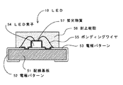
図3は従来のLED50の縦断面図である。51は両面銅箔張りのガラスエポキシ樹脂等より成る配線基板であり、配線基板51の両面銅箔部にはメッキレジストをラミネートし、露光現像して配線パターンを形成し、更にその上に金メッキ等の表面処理を施してある。52は、上面電極52aから側面電極52bを経由して下面電極52cに至る配線パターンである一方の電極パターンであり、53は、同じく上面電極53aから側面電極53bを経由して下面電極53cに至る他方の電極パターンである。
【0004】
54は、上面電極52aに一方の電極を銀ペーストによりダイボンディングしたGaN系の青色LED素子である。55はAu線等より成るワイヤであり、ワイヤ55によりLED素子54の他方の電極と上面電極53aとがワイヤボンディングにより接続されている。56は、LED素子54、LED素子54の接続部及びワイヤ55等の保護と、LED素子54の発光を効果的にすることのために封止している、透光性のエポキシ樹脂等から成る封止樹脂である。封止樹脂56には予め57の蛍光物質(YAG蛍光体)を含有させてある。
【0005】
LED50を発光させると、LED素子54を発して封止樹脂56の中で蛍光物質に当たった青色光は黄色に変化して出射し、蛍光物質に当たらなかった光は青色のまま出射することになるため、これら黄色と青色とが混色となって白色光となる。また、封止樹脂中に蛍光物質を含有させることにより白色光をフィルターすることで、パステル調の発光色を得ることができるというものである。
【0006】
【発明が解決しようとする課題】
しかしながら、従来のこのようなLEDでは、蛍光物質は、封止樹脂よりも比重が大きいために、樹脂に混入後キュアー炉で樹脂を硬化させる過程において蛍光物質が沈殿してしまい、樹脂内に均一に拡散させることが困難であった。また、蛍光物質を定量塗布することが困難であるため、その量のバラツキによって発光色の色調のバラツキが発生し、量産上不良品の選別工程が欠かせなかった。従ってコストアップを招くので、LEDの色調のバラツキをいかに少なくしてコストを押さえるかが課題であった。
【0007】
上記発明は、このような従来の問題を解決するためになされたものであり、その目的は、発光色のバラツキを改良して量産に適するLEDの製造方法を提供するものである。
【0008】
【課題を解決するための手段】
前述した目的を達成するための本発明の手段は、外部接続端子を有する配線基板上に青色の発光素子を搭載し、該発光素子を蛍光物質を含有した樹脂で封止した表面実装型発光ダイオードを製造する方法において、前記配線基板上の少なくとも前記発光素子の周面に、前記蛍光物質をノズルからの吐出を容易にし、かつ前記蛍光物質の沈殿が無くなる程度に、前記蛍光物質の比重と近似した比重を持つ媒体と混合してインクジェット方式により塗布する工程と、前記蛍光物質を塗布した配線基板を樹脂で封止する工程を有することを特徴とする表面実装型発光ダイオードの製造方法。
【0010】
【発明の実施の形態】
以下、本発明の実施の形態を図面に基づいて詳細に説明する。まず、この実施の形態の構成について説明する。図1は本発明の実施の形態であるLEDの断面図、図2はこのLEDの製造方法を示す断面図である。
【0011】
図1において、10は表面実装型LEDである。LED10が従来のLED50と異なるところは、蛍光物質の塗布形態及び蛍光物質の塗布方法である。その他の構成はLED50と同じなので、同じ構成要素にはLED50と同じ符号と名称を付して詳細な説明を省略する。蛍光物質57は予めLED54の周面及び配線基板51上に均一に定量塗布されている。
【0012】
次に、この実施の形態の作用を説明する。GaN系のLED素子54を発した青色光は、LED素子54の表面に均一に一定量存在する蛍光物質57に当たったものは黄色に変化して出射し、蛍光物質57に当たらなかった光は青色のまま出射することになるため、これら黄色と青色が混色することにより白色光となる。この場合に、蛍光物質がLED素子54の周面に均一に、一定量塗布されているために、その量による色調のバラツキが生じない。また、蛍光物質の量、即ち厚みを精密に制御できることから、青みがかった白色、黄みがかった白色等、所望の白色光を得ることができる。また、パステル色についても同様である。
【0013】
次に、このLED10の製造方法について、中でもインクジェット方式を採用して蛍光物質57を塗布する工程について説明する。図2において、20はインクジェット方式により蛍光物質57を吐出するノズルである。まず、LED素子54を搭載後の配線基板51に対して、ノズル20をLED素子54の上面に近接させて蛍光物質57を吐出する。このとき、ノズル20は揺動動作をする。蛍光物質57の吐出を容易にするために、蛍光物質57は蛍光物質57の比重と近似した比重を持つ媒体に予め混合しておく。LED10を製造する全体の工程には、配線基板51の多数個取りが可能な、集合状態の配線基板を用いて、配線基板上で同時多数個の製造方式がとられる。
【0014】
次に、本実施の形態であるLED10の効果について説明する。蛍光物質57の塗布と封止成形とを別工程にしたので、封止作業中の蛍光物質の沈殿が無くなった。また、インクジェット方式を採用して、直接LED素子54周面に蛍光物質57を塗布するようにしたので、蛍光物質57を均一に定量塗布にすることができる。従って、蛍光物質の量を微調整することが可能となり、微妙な色調の調整が容易になって、白色は無論のこと、中間色であるパステル調の発光色も容易に得られるようになった。そして、従来必要であった色調の選別工程を廃止できた。なお、多数個取りのできる集合基板である配線基板を用いて、同時多数個の処理ができるので、製造コストを削減できる。
【0015】
【発明の効果】
以上説明したように、本発明によれば、配線基板上に青色の発光素子を搭載し、該発光素子を蛍光物質を含有した樹脂で封止した表面実装型発光ダイオードにおいて、前記配線基板上の少なくとも前記発光素子の周面に蛍光物質が塗布されており、その上から樹脂により成形封止したので、蛍光物質の量と分布が均一となり、バラツキが減って、白色やパステル調の発光色を有するLEDが安定して量産できるようになった。
【0016】
蛍光物質を発光素子に塗布するのに、インクジェット方式を採用したので、蛍光物質を均一に塗布でき、蛍光物質の量を微調整することが可能となって、容易に白色、パステル色調の発光を得ることができるようになった。
【図面の簡単な説明】
【図1】本発明の実施の形態であるLEDの断面図である。
【図2】本発明の実施の形態であるLEDの製造方法を示す断面図である。
【図3】従来のLEDの縦断面図である。
【符号の説明】
10 発光ダイオード(LED)
51 配線基板
52、53 電極パターン
54 LED素子(発光素子)
56 封止樹脂
57 蛍光物質[0001]
BACKGROUND OF THE INVENTION
The present invention (hereinafter abbreviated as LED) surface mount light emitting diode, a method for manufacturing a particularly white LED and pastel LE D.
[0002]
[Prior art]
LEDs form a PN junction on a compound semiconductor wafer such as GaP or GaN, and obtain visible or near-infrared light emission through a forward current, and have been widely used for display, communication, measurement, control, etc. Applied. However, such conventional LEDs have only a limited color tone. In order to obtain a desired color light source, there has been an attempt to contain a fluorescent substance or a colorant in a sealing resin such as an epoxy resin or a silicone resin. An example of such a conventional LED will be described with reference to the drawings.
[0003]
FIG. 3 is a longitudinal sectional view of a
[0004]
[0005]
When the
[0006]
[Problems to be solved by the invention]
However, in such a conventional LED, since the specific gravity of the fluorescent material is larger than that of the sealing resin, the fluorescent material is precipitated in the process of curing the resin in the curing furnace after being mixed in the resin, and uniform in the resin. Difficult to diffuse into. In addition, since it is difficult to apply the fluorescent substance in a fixed amount, the variation in the amount of emitted light causes a variation in the color of the luminescent color, which makes it necessary to select a defective product in mass production. Therefore, since the cost is increased, it has been a problem how to reduce the variation in the color tone of the LED to suppress the cost.
[0007]
The above invention has been made to solve such conventional problems, and its object is to provide a manufacturing method of LE D suitable for mass production to improve the dispersion of the emission color.
[0008]
[Means for Solving the Problems]
The means of the present invention for achieving the above-described object includes a surface-mounted light-emitting diode in which a blue light-emitting element is mounted on a wiring board having external connection terminals, and the light-emitting element is sealed with a resin containing a fluorescent material. In the method of manufacturing the phosphor material, the phosphor material is easily discharged from the nozzle on at least the peripheral surface of the light emitting element, and approximate to the specific gravity of the phosphor material to the extent that precipitation of the phosphor material is eliminated. A method of manufacturing a surface-mounted light-emitting diode, comprising: a step of mixing with a medium having a specific gravity and applying the mixture by an inkjet method; and a step of sealing the wiring substrate coated with the fluorescent material with a resin.
[0010]
DETAILED DESCRIPTION OF THE INVENTION
Hereinafter, embodiments of the present invention will be described in detail with reference to the drawings. First, the configuration of this embodiment will be described. FIG. 1 is a cross-sectional view of an LED according to an embodiment of the present invention, and FIG. 2 is a cross-sectional view showing a method for manufacturing the LED.
[0011]
In FIG. 1, 10 is a surface-mounted LED. The
[0012]
Next, the operation of this embodiment will be described. As for the blue light emitted from the GaN-based
[0013]
Next, regarding the manufacturing method of the
[0014]
Next, the effect of LED10 which is this Embodiment is demonstrated. Since the application of the
[0015]
【The invention's effect】
As described above, according to the present invention, in a surface-mounted light emitting diode in which a blue light emitting element is mounted on a wiring board and the light emitting element is sealed with a resin containing a fluorescent material, At least the peripheral surface of the light-emitting element is coated with a fluorescent material, and molded and sealed with resin from above, so that the amount and distribution of the fluorescent material become uniform, variation is reduced, and white or pastel tone emission color is achieved. The LED it has been able to be mass-produced stably.
[0016]
Since the inkjet method is used to apply the fluorescent material to the light emitting element, the fluorescent material can be applied uniformly and the amount of the fluorescent material can be finely adjusted, and light emission in white and pastel colors can be easily performed. Can now get.
[Brief description of the drawings]
FIG. 1 is a cross-sectional view of an LED according to an embodiment of the present invention.
FIG. 2 is a cross-sectional view showing a method for manufacturing an LED according to an embodiment of the present invention.
FIG. 3 is a longitudinal sectional view of a conventional LED.
[Explanation of symbols]
10 Light emitting diode (LED)
51
56
Claims (1)
Priority Applications (1)
| Application Number | Priority Date | Filing Date | Title |
|---|---|---|---|
| JP2002056667A JP4039552B2 (en) | 2002-03-01 | 2002-03-01 | Manufacturing method of surface mount type light emitting diode |
Applications Claiming Priority (1)
| Application Number | Priority Date | Filing Date | Title |
|---|---|---|---|
| JP2002056667A JP4039552B2 (en) | 2002-03-01 | 2002-03-01 | Manufacturing method of surface mount type light emitting diode |
Publications (2)
| Publication Number | Publication Date |
|---|---|
| JP2003258310A JP2003258310A (en) | 2003-09-12 |
| JP4039552B2 true JP4039552B2 (en) | 2008-01-30 |
Family
ID=28667116
Family Applications (1)
| Application Number | Title | Priority Date | Filing Date |
|---|---|---|---|
| JP2002056667A Expired - Fee Related JP4039552B2 (en) | 2002-03-01 | 2002-03-01 | Manufacturing method of surface mount type light emitting diode |
Country Status (1)
| Country | Link |
|---|---|
| JP (1) | JP4039552B2 (en) |
Families Citing this family (14)
| Publication number | Priority date | Publication date | Assignee | Title |
|---|---|---|---|---|
| JP4627177B2 (en) | 2004-11-10 | 2011-02-09 | スタンレー電気株式会社 | LED manufacturing method |
| JP4792751B2 (en) * | 2005-01-26 | 2011-10-12 | 日亜化学工業株式会社 | Light emitting device and manufacturing method thereof |
| JP2006245020A (en) * | 2005-02-28 | 2006-09-14 | Sharp Corp | Light emitting diode element and manufacturing method thereof |
| CN100386897C (en) * | 2005-05-31 | 2008-05-07 | 李锋 | A method of manufacturing a light-emitting diode bracket |
| KR101346341B1 (en) | 2007-05-08 | 2013-12-31 | 서울반도체 주식회사 | Light emitting device with submount and method for fabricating the same |
| JP5084015B2 (en) * | 2007-05-15 | 2012-11-28 | シチズン電子株式会社 | Manufacturing method of light emitting diode |
| KR100978566B1 (en) * | 2008-02-29 | 2010-08-27 | 삼성엘이디 주식회사 | Side release LED package and manufacturing method thereof |
| KR101038883B1 (en) | 2009-02-17 | 2011-06-02 | 삼성엘이디 주식회사 | Light emitting diode package and manufacturing method thereof |
| KR101601622B1 (en) | 2009-10-13 | 2016-03-09 | 삼성전자주식회사 | Light emitting diode device, light emitting device and method of manufacturing light emitting diode device |
| USD749051S1 (en) | 2012-05-31 | 2016-02-09 | Cree, Inc. | Light emitting diode (LED) package |
| US9349929B2 (en) | 2012-05-31 | 2016-05-24 | Cree, Inc. | Light emitter packages, systems, and methods |
| US10439112B2 (en) | 2012-05-31 | 2019-10-08 | Cree, Inc. | Light emitter packages, systems, and methods having improved performance |
| USD709464S1 (en) | 2012-05-31 | 2014-07-22 | Cree, Inc. | Light emitting diode (LED) package |
| JP5959575B2 (en) * | 2014-06-30 | 2016-08-02 | ミネベア株式会社 | Planar illumination device and manufacturing method thereof |
-
2002
- 2002-03-01 JP JP2002056667A patent/JP4039552B2/en not_active Expired - Fee Related
Also Published As
| Publication number | Publication date |
|---|---|
| JP2003258310A (en) | 2003-09-12 |
Similar Documents
| Publication | Publication Date | Title |
|---|---|---|
| JP3768864B2 (en) | Surface mount type light emitting diode and manufacturing method thereof | |
| JP4039552B2 (en) | Manufacturing method of surface mount type light emitting diode | |
| JP4789350B2 (en) | Manufacturing method of light emitting diode | |
| US8378375B2 (en) | Light emitting apparatus having a partition | |
| JP4673986B2 (en) | Manufacturing method of surface mounted light emitting diode | |
| CN101312185B (en) | Light emitting device and method for manufacturing the same | |
| JP3832877B2 (en) | Ceramic LED package and manufacturing method thereof | |
| JP4003866B2 (en) | Surface mount type light emitting diode and manufacturing method thereof | |
| JP2004128424A5 (en) | ||
| CN101960626A (en) | Light emitting module and display device having the same | |
| CN109698190B (en) | A processing method of color display lamp beads | |
| JP6100778B2 (en) | LED mixing chamber with a reflective wall formed in the slot | |
| KR20070012501A (en) | Light emitting device and manufacturing method | |
| JP2004153261A (en) | Screen printing method of luminescent base layer | |
| US9379292B2 (en) | LED light source packaging method, LED light source package structure and light source module | |
| JP2012142428A (en) | Light-emitting device and method of manufacturing light-emitting device | |
| KR100558080B1 (en) | Phosphor, Light Emitting Diode Using the Same, and Manufacturing Method Thereof | |
| JP2001024238A (en) | Multicolor light emitting diode | |
| KR20090034412A (en) | Light emitting chip and manufacturing method thereof | |
| JP3986327B2 (en) | Method for manufacturing light emitting device | |
| KR20080055549A (en) | Manufacturing method of LED package | |
| JP3114129U (en) | White light emitting diode | |
| JP2003077317A (en) | LED lamp | |
| KR100954858B1 (en) | A high-luminance led package and method for manufacturing thereof | |
| KR100748707B1 (en) | Manufacturing method of light emitting device |
Legal Events
| Date | Code | Title | Description |
|---|---|---|---|
| A621 | Written request for application examination |
Free format text: JAPANESE INTERMEDIATE CODE: A621 Effective date: 20040514 |
|
| A977 | Report on retrieval |
Free format text: JAPANESE INTERMEDIATE CODE: A971007 Effective date: 20061124 |
|
| A131 | Notification of reasons for refusal |
Free format text: JAPANESE INTERMEDIATE CODE: A131 Effective date: 20061129 |
|
| A521 | Request for written amendment filed |
Free format text: JAPANESE INTERMEDIATE CODE: A523 Effective date: 20070122 |
|
| A131 | Notification of reasons for refusal |
Free format text: JAPANESE INTERMEDIATE CODE: A131 Effective date: 20070226 |
|
| A521 | Request for written amendment filed |
Free format text: JAPANESE INTERMEDIATE CODE: A523 Effective date: 20070419 |
|
| A02 | Decision of refusal |
Free format text: JAPANESE INTERMEDIATE CODE: A02 Effective date: 20070604 |
|
| A521 | Request for written amendment filed |
Free format text: JAPANESE INTERMEDIATE CODE: A523 Effective date: 20070626 |
|
| A911 | Transfer to examiner for re-examination before appeal (zenchi) |
Free format text: JAPANESE INTERMEDIATE CODE: A911 Effective date: 20070806 |
|
| A131 | Notification of reasons for refusal |
Free format text: JAPANESE INTERMEDIATE CODE: A131 Effective date: 20070823 |
|
| A521 | Request for written amendment filed |
Free format text: JAPANESE INTERMEDIATE CODE: A523 Effective date: 20070911 |
|
| TRDD | Decision of grant or rejection written | ||
| A01 | Written decision to grant a patent or to grant a registration (utility model) |
Free format text: JAPANESE INTERMEDIATE CODE: A01 Effective date: 20071031 |
|
| A61 | First payment of annual fees (during grant procedure) |
Free format text: JAPANESE INTERMEDIATE CODE: A61 Effective date: 20071101 |
|
| FPAY | Renewal fee payment (event date is renewal date of database) |
Free format text: PAYMENT UNTIL: 20101116 Year of fee payment: 3 |
|
| R150 | Certificate of patent or registration of utility model |
Free format text: JAPANESE INTERMEDIATE CODE: R150 Ref document number: 4039552 Country of ref document: JP Free format text: JAPANESE INTERMEDIATE CODE: R150 |
|
| FPAY | Renewal fee payment (event date is renewal date of database) |
Free format text: PAYMENT UNTIL: 20131116 Year of fee payment: 6 |
|
| R250 | Receipt of annual fees |
Free format text: JAPANESE INTERMEDIATE CODE: R250 |
|
| R250 | Receipt of annual fees |
Free format text: JAPANESE INTERMEDIATE CODE: R250 |
|
| R250 | Receipt of annual fees |
Free format text: JAPANESE INTERMEDIATE CODE: R250 |
|
| LAPS | Cancellation because of no payment of annual fees |