JP4036498B2 - Active matrix liquid crystal display device - Google Patents
Active matrix liquid crystal display device Download PDFInfo
- Publication number
- JP4036498B2 JP4036498B2 JP6713397A JP6713397A JP4036498B2 JP 4036498 B2 JP4036498 B2 JP 4036498B2 JP 6713397 A JP6713397 A JP 6713397A JP 6713397 A JP6713397 A JP 6713397A JP 4036498 B2 JP4036498 B2 JP 4036498B2
- Authority
- JP
- Japan
- Prior art keywords
- liquid crystal
- pixel electrode
- crystal display
- display device
- active matrix
- Prior art date
- Legal status (The legal status is an assumption and is not a legal conclusion. Google has not performed a legal analysis and makes no representation as to the accuracy of the status listed.)
- Expired - Fee Related
Links
Images
Landscapes
- Liquid Crystal (AREA)
- Devices For Indicating Variable Information By Combining Individual Elements (AREA)
Description
【0001】
【発明の属する技術分野】
本発明は、AV・OA機器などの平面ディスプレイとして用いることのできるアクティブマトリクス型液晶表示装置に関するものである。
【0002】
【従来の技術】
現在、液晶を用いた表示装置は、ビデオカメラのビューファインダーやポケットTVさらには高精細投写型TV、パソコン、ワープロなどの情報表示端末など種々の分野で応用されてきており、開発、商品化が活発に行われている。
【0003】
特に、スイッチング素子として薄膜トランジスタ(TFT)を用いたアクティブマトリクス型方式のTN(Twisted Nematic)液晶表示装置は大容量の表示を行っても高いコントラストが保たれるという大きな特徴をもち、近年は市場の要望の極めて高いラップトップパソコンやノートパソコン、さらにはエンジニアリングワークステーション用の大型・大容量フルカラーディスプレイの本命として開発、商品化が盛んである。
【0004】
このようなアクティブマトリクス方式の液晶表示素子において、広く用いられている液晶表示モードのTN(Twisted Nematic )方式は液晶層を挟持する電極基板間で液晶分子が90゜捻れた構造をとるパネルを2枚の偏光板により挟んだものである。
【0005】
2枚の偏光板は互いの偏光軸方向が直交し、一方の偏光板はその偏光軸が一方の基板に接している液晶分子の長軸方向と平行か垂直になるように配置されている。電圧無印加の場合は白表示であるが、2枚の基板間すなわち液晶パネルに対して垂直方向に電圧を印加していくと、徐々に光透過率が低下して黒表示となる。
【0006】
このような表示特性が得られるのは、液晶パネルに電圧を印加すると液晶分子は捻れ構造をほどきながら電界の向きに配列しようとし、この分子の配列状態により、パネルを透過してくる光の偏光状態が変わり、光の透過率が変調されるからである。
【0007】
しかし、同じ分子配列状態でも、液晶パネルに入射してくる光の入射方向によって透過光の偏光状態は変化するので、入射方向に対応して光の透過率は異なってくる。すなわち、液晶パネルの特性は視角依存性を持つ。この視角特性は主視角方向(液晶層の中間層における液晶分子の長軸方向)に対し視点を斜めに傾けると輝度の逆転現象を引き起こし、液晶パネルの画質上、重要な課題となっている。
【0008】
この課題を解決するために、TN型液晶表示方式のように基板垂直方向に電界を印加するのではなく、液晶に印加する方向を基板に対してほぼ平行な方向とするIPS(In-Plane Switching )方式があり、例えば特公昭63−21907号公報や特開平6−160878号公報により提案されている。
【0009】
【発明が解決しようとする課題】
従来のIPS方式の液晶表示装置のアレイ基板の画素部の構成を図3(a)に示す。図3(b)は図3(a)図の一点鎖線での液晶表示装置の断面構成の概略断面図を示す。
【0010】
この図に示すように、複数の走査配線2および信号配線7が直交するように形成され、走査配線2と信号配線7の各交差点に対応してスイッチング素子であるTFT11が設けられる。隣接する2つの走査配線2と隣接する2つの信号配線7に囲まれる1画素において、複数、例えば2つの画素電極8が信号配線7に略平行に形成されている。信号配線7と画素電極8の間および隣接する画素電極8の間には、複数、例えば3つの共通電極3が櫛形状に形成され、かつ画素電極8と咬合している。蓄積容量部9は画素電極8の間で、かつ走査配線2の上部に形成されている。
【0011】
次に製作工程を説明する。
ガラス基板1の上にアルミニウム(Al)を積層させ、フォトリソグラフィ法によって走査配線2と共通電極3を同時にパターン形成する。走査配線2と共通電極3の上にはTFTのゲート絶縁膜として働く窒化シリコン(SiNx)の第1絶縁体層4を積層させる。さらに第1絶縁体層4の上にTFTのスイッチ機能を司るアモルファスシリコン(α−Si)の半導体層5が積層されている。その後、TFTのチャンネル保護膜として窒化シリコン(SiNx)の第2絶縁体層6を積層、パターン形成する。そしてn+アモルファスシリコン(n+−α−Si)、チタン(Ti)、アルミニウム(Al)の3層を連続堆積させ、一括パターン形成を行い、信号配線7、画素電極8と蓄積容量部9を図のように形成した。ここでn+アモルファスシリコン(n+−α−Si)は半導体層5と信号配線7、画素電極8とのオーミックコンタクトをとるために、チタン(Ti)はアルミニウム(Al)がアモルファスシリコン(α−Si)の半導体層5に拡散するのを防止するために設けられた。さらにTFT保護膜として窒化シリコン(SiNx)の第3絶縁体層10を積層させる。
【0012】
以上のように構成されたアレイ基板12と対向基板13とに配向膜を塗布し、ラビング処理を行う。そしてアレイ基板12と対向基板13とを一定のギャップを隔てて貼り合わせ、その間には液晶を注入し、液晶層14を形成する。対向基板13には走査配線2と信号配線7に対応する位置に遮光膜15が存在するが、共通電極3と画素電極8に対応する位置に遮光膜15が存在しない。
【0013】
しかしながら、上記構成では信号配線7と画素電極8との膜厚が同じである。信号配線7は断線不良に裕度を持たせるためや、配線抵抗を小さくするために膜厚を厚くする必要性がある。したがって画素電極8の膜厚も厚くなり、画素電極8の近傍ではラビング処理が行われない。そのためパネル表示では、その部分で非配向光抜けが起こり、コントラストが低下してしまう。また画素電極8の最表面が反射率の高いアルミニウム(Al)で形成されているため、パネル外光を反射してしまい、さらにコントラストが低下する問題も起こる。
【0014】
【課題を解決するための手段】
本発明のアクティブマトリクス型液晶表示装置は、マトリクス状に配置された複数の信号配線及び走査配線と、前記信号配線と走査配線との各交差点に設けられた一つ以上のスイッチング素子と、前記スイッチング素子に接続された画素電極と、前記画素電極と咬合して形成された共通電極と、ラビング処理が施された配向膜とを有するアレイ基板と、前記アレイ基板に対向して配置された対向基板と、前記アレイ基板と前記対向基板との間に挟持された液晶層とを具備し、前記液晶層に、前記アレイ基板に対してほぼ平行な方向の電界が印加されるアクティブマトリクス型液晶表示装置であって、前記信号配線は複数層から成り、前記画素電極が前記複数層の最上層を除いた層から形成されることにより、前記画素電極の膜厚が前記信号配線の膜厚より薄いことを特徴とする。
【0015】
この本発明によると、IPS方式の液晶表示装置において、画素電極の膜厚を信号配線の膜厚より薄くすることにより、画素電極の近傍でもラビング処理が可能となり、画素電極近傍において、非配向光抜けは起こらない。
【0016】
【発明の実施の形態】
本発明のアクティブマトリクス型液晶表示装置は、マトリクス状に配置された複数の信号配線及び走査配線と、前記信号配線と走査配線との各交差点に設けられた一つ以上のスイッチング素子と、前記スイッチング素子に接続された画素電極と、前記画素電極と咬合して形成された共通電極と、ラビング処理が施された配向膜とを有するアレイ基板と、前記アレイ基板に対向して配置された対向基板と、前記アレイ基板と前記対向基板との間に挟持された液晶層とを具備し、前記液晶層に、前記アレイ基板に対してほぼ平行な方向の電界が印加されるアクティブマトリクス型液晶表示装置であって、前記信号配線は複数層から成り、前記画素電極が前記複数層の最上層を除いた層から形成されることにより、前記画素電極の膜厚が前記信号配線の膜厚より薄い構成としたことにより、画素電極の近傍でもラビング処理が可能となる。したがってパネル表示では、画素電極近傍において非配向光抜けは起こらず、高いコントラストの画面が得られる。
【0017】
また、前記信号配線の最上層はアルミニウム層であることが好ましく、さらに、前記画素電極の最表面がアルミニウムより反射率の小さい導電性材料で形成されるか、または前記画素電極が透明導電性材料で形成されることにより、パネル外光の反射が抑えられ、より高いコントラストの画面が得られる。また、信号配線の少なくとも一部と画素電極とが、同一の膜の上に、この膜に接触するように形成される。
【0018】
以下、本発明のアクティブマトリクス型液晶表示装置を各実施の形態に基づいて説明する。
(実施の形態1)
図1(a)は本発明の(実施の形態1)におけるアレイ基板の画素部の平面構成を概略的に示し、図1(b)は図1(a)図の一点鎖線での液晶表示装置の断面構成の概略断面図を示す。
【0019】
図1に示すガラスアレイ基板1には、複数の走査配線2および信号配線7が直交するように形成され、走査配線2と信号配線7の各交差点に対応してスイッチング素子であるTFT11が設けられる。隣接する2つの走査配線2と隣接する2つの信号配線7に囲まれる1画素において、複数、例えば2つの画素電極8が信号配線7に略平行に形成されている。
【0020】
信号配線7と画素電極8の間および隣接する画素電極8の間には、複数、例えば3つの共通電極3が櫛形状に形成され、かつ画素電極8と咬合している。蓄積容量部9は画素電極8の間で、かつ走査配線2の上部に形成されている。
【0021】
製作工程は以下の通りである。
走査配線2としてアルミニウムを用いて、フォトリソグラフィ法によってガラス基板1の上に図のようにそれぞれ所定の間隔を隔てて、略平行にパターン形成されている。それと同時に、隣接する2つの走査配線2の間に互いに略平行な共通電極3がパターン形成されている。
【0022】
なお、走査配線2と共通電極3の膜厚は150nmであり、材料はアルミニウムに限定せず、クロム(Cr)、アルミニウムを主成分とする金属など導電性単層膜または多層膜を用いてもよい。
【0023】
走査配線2、共通電極3の上には、スイッチング素子として機能するTFT11のゲート絶縁膜として働く、例えば窒化シリコン(SiNx)などの第1絶縁体層4が積層されている。さらに、第1絶縁体層4の上にはTFTのスイッチ機能を司る、例えばアモルファスシリコン(α−Si)の半導体層5を積層させる。その後、TFTのチャンネル保護膜として窒化シリコン(SiNx)の第2絶縁体層6を積層、パターン形成する。そしてn+アモルファスシリコン(n+−α−Si)、チタン(Ti)の2層を連続堆積させ、ドライエッチングによって一括パターン形成を行い、画素電極8と蓄積容量部9を図のように形成した。相互に隣接する2つの共通電極3の間に、共通電極3と略平行となるように画素電極8が形成されている。ここでチタン(Ti)の膜厚は100nmとした。
【0024】
さらに、アルミニウム(Al)を300nm堆積させ、これを用いて信号配線7が走査配線2に対して略直交し、かつ、それぞれ略平行になるようにウエットエッチングによってパターン形成された。
【0025】
第1絶縁体層4と半導体層5を挟んで走査配線2の上には、2つの画素電極8を接続するように蓄積容量部9がオーバーラップして形成された。この蓄積容量部9は画素に供給された電圧を保持するために設けられたものである。そして保護膜として、例えば窒化シリコン(SiNx)などの第3絶縁体層10が積層された。
【0026】
以上のように構成されたアレイ基板12と対向基板13とに配向膜を塗布し、ラビング処理を行った。そしてアレイ基板12と対向基板13とを3μmのギャップを隔てて貼り合わせ、その間には液晶を注入し、液晶層14を形成した。このように画素電極8の膜厚が信号配線7より200nm薄くなり、画素電極8の近傍でもラビング処理が可能となるとともに、アルミニウムより反射率の低いチタンで画素電極8が形成される構成となる。この液晶表示装置の点灯画像検査を行ったところ、画素電極8の近傍に非配向光抜けも無く、コントラストの高い画像が得られることが確認された。
【0027】
なお、画素電極8の膜厚は30〜200nmの範囲で良く、また材料はチタン以外のタンタル(Ta)、クロム(Cr)、モリブデン(Mo)などのアルミニウムより反射率の低い導電性材料でもよく、または透明導電性材料のインジウム−錫酸化物(ITO)でもかまわない。
【0028】
また、本構成は共通電極3が信号配線7と同じ層に形成される場合においても、画素電極8に関する事項を共通電極3に当てはめることで有効である。
(実施の形態2)
図2(a)は本発明の(実施の形態2)におけるアレイ基板の画素部の平面構成を概略的に示し、図2(b)は図2(a)図の一点鎖線での液晶表示装置の断面構成の概略断面図を示す。上記第1の実施の形態の場合と共通する部分についてはその説明を省略し、異なる部分について述べる。
【0029】
(実施の形態2)は、第2絶縁体層6のパターン形成後、n+アモルファスシリコン(n+−α−Si)、チタン(Ti)の2層を連続堆積させ、ドライエッチングによって一括パターン形成を行い、画素電極8、蓄積容量部9および信号配線部を図のように形成した。
【0030】
さらに、アルミニウム(Al)を堆積させ、チタン(Ti)で形成した前記の信号配線部に重畳するように、ウエットエッチングによって信号配線7を形成した。この信号配線7をチタン/アルミニウム(Ti/Al)の2層にする構成により、(実施の形態1)と比較して、信号配線7の断線不良に対する裕度をより大きくすることができ、また配線抵抗をより小さくすることができる。この液晶表示装置の点灯画像検査を行ったところ、画素電極8の近傍に非配向光抜けも無く、コントラストの高い画像が得られることが確認された。
【0031】
【発明の効果】
以上のように本発明のアクティブマトリクス型液晶表示装置は、広い視角で良好な多階調表示を実現できるIPS方式の液晶表示装置において、画素電極の膜厚を信号配線の膜厚より薄くするという簡易な構成によって、断線不良に対する裕度を小さくしたり、また配線抵抗を大きくしたりすることなく、画素電極の近傍の非配向光抜けを防止でき、コントラストの高い画像を得ることができる。
【図面の簡単な説明】
【図1】本発明の(実施の形態1)のアクティブマトリクス液晶表示装置におけるアレイ基板の画素部の平面構成を概略的に示す平面図と断面図
【図2】本発明の(実施の形態2)のアクティブマトリクス液晶表示装置におけるアレイ基板の画素部の平面構成を概略的に示す平面図と断面図
【図3】従来のアクティブマトリクス液晶表示装置におけるアレイ基板の画素部の平面構成を概略的に示す平面図と断面図
【符号の説明】
1 ガラス基板
2 走査配線
3 共通電極
4 第1絶縁体層
5 半導体層
6 第2絶縁体層
7 信号配線
8 画素電極
9 蓄積容量部
10 第3絶縁体層
11 TFT
12 アレイ基板
13 対向基板
14 液晶層
15 遮光膜[0001]
BACKGROUND OF THE INVENTION
The present invention relates to an active matrix liquid crystal display device that can be used as a flat display such as an AV / OA device.
[0002]
[Prior art]
Currently, display devices using liquid crystals have been applied in various fields such as video camera viewfinders, pocket TVs, high-definition projection TVs, personal computers, word processors, and other information display terminals. It is active.
[0003]
In particular, an active matrix type TN (Twisted Nematic) liquid crystal display device using a thin film transistor (TFT) as a switching element has a great feature that high contrast is maintained even when a large capacity display is performed. It has been actively developed and commercialized as a favorite of large-scale, large-capacity full-color displays for laptop computers, notebook computers, and engineering workstations with extremely high demands.
[0004]
In such an active matrix type liquid crystal display element, a widely used liquid crystal display mode TN (Twisted Nematic) type is a panel having a structure in which liquid crystal molecules are twisted by 90 ° between electrode substrates sandwiching a liquid crystal layer. It is sandwiched between two polarizing plates.
[0005]
The two polarizing plates are arranged such that their polarization axes are orthogonal to each other, and one polarizing plate is arranged so that its polarization axis is parallel or perpendicular to the major axis direction of the liquid crystal molecules in contact with one substrate. When no voltage is applied, white display is performed. However, when a voltage is applied in the vertical direction between two substrates, that is, with respect to the liquid crystal panel, the light transmittance gradually decreases to display black.
[0006]
Such display characteristics are obtained when a voltage is applied to the liquid crystal panel, the liquid crystal molecules attempt to align in the direction of the electric field while unwinding the twisted structure, and the alignment state of the molecules causes the light transmitted through the panel to be aligned. This is because the polarization state changes and the light transmittance is modulated.
[0007]
However, even in the same molecular arrangement state, the polarization state of the transmitted light changes depending on the incident direction of the light incident on the liquid crystal panel. Therefore, the light transmittance varies depending on the incident direction. That is, the characteristics of the liquid crystal panel have a viewing angle dependency. This viewing angle characteristic causes a luminance reversal phenomenon when the viewpoint is tilted with respect to the main viewing angle direction (the major axis direction of the liquid crystal molecules in the intermediate layer of the liquid crystal layer), which is an important issue in the image quality of the liquid crystal panel.
[0008]
In order to solve this problem, an IPS (In-Plane Switching) in which the direction applied to the liquid crystal is a direction substantially parallel to the substrate, rather than applying an electric field in the direction perpendicular to the substrate as in the TN liquid crystal display system. For example, Japanese Patent Publication No. 63-21907 and Japanese Patent Laid-Open No. 6-160878.
[0009]
[Problems to be solved by the invention]
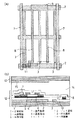
FIG. 3A shows a configuration of a pixel portion of an array substrate of a conventional IPS liquid crystal display device. FIG. 3B is a schematic cross-sectional view of the cross-sectional configuration of the liquid crystal display device taken along the alternate long and short dash line in FIG.
[0010]
As shown in this figure, a plurality of
[0011]
Next, the manufacturing process will be described.
Aluminum (Al) is laminated on the
[0012]
An alignment film is applied to the
[0013]
However, in the above configuration, the
[0014]
[Means for Solving the Problems]
The active matrix liquid crystal display device of the present invention includes a plurality of signal lines and scanning lines arranged in a matrix, one or more switching elements provided at each intersection of the signal lines and the scanning lines, and the switching An array substrate having a pixel electrode connected to the element, a common electrode formed by meshing with the pixel electrode, and an alignment film subjected to rubbing treatment, and a counter substrate disposed to face the array substrate And an active matrix liquid crystal display device in which an electric field in a direction substantially parallel to the array substrate is applied to the liquid crystal layer. a is, the signal line comprises a plurality of layers, wherein by which the pixel electrode is formed from a layer other than the uppermost layer of the plural layers, the thickness of the pixel electrode is the signal distribution Wherein the thinner than the thickness of.
[0015]
According to the present invention, in the IPS liquid crystal display device, by making the film thickness of the pixel electrode thinner than that of the signal wiring, the rubbing process can be performed in the vicinity of the pixel electrode. Omission does not occur.
[0016]
DETAILED DESCRIPTION OF THE INVENTION
The active matrix liquid crystal display device of the present invention includes a plurality of signal lines and scanning lines arranged in a matrix, one or more switching elements provided at each intersection of the signal lines and the scanning lines, and the switching An array substrate having a pixel electrode connected to the element, a common electrode formed by meshing with the pixel electrode, and an alignment film subjected to rubbing treatment, and a counter substrate disposed to face the array substrate And an active matrix liquid crystal display device in which an electric field in a direction substantially parallel to the array substrate is applied to the liquid crystal layer. a is, the signal line comprises a plurality of layers, wherein by which the pixel electrode is formed from a layer other than the uppermost layer of the plural layers, the thickness of the pixel electrode is the signal distribution By thin structure than the thickness of the the, it is possible to rubbing treatment in the vicinity of the pixel electrode. Therefore, in panel display, non-aligned light leakage does not occur in the vicinity of the pixel electrode, and a high contrast screen can be obtained.
[0017]
Further, the signal uppermost preferably aluminum layer der Rukoto wiring, furthermore, the outermost surface or small conductive reflective material of aluminum Ru is formed by, or the pixel electrode is a transparent conductive the pixel electrode By using the material, reflection of light outside the panel is suppressed, and a screen with higher contrast can be obtained. Further, at least part of the signal wiring and the pixel electrode are formed on the same film so as to be in contact with the film.
[0018]
Hereinafter, an active matrix liquid crystal display device of the present invention will be described based on each embodiment.
(Embodiment 1)
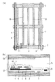
FIG. 1A schematically shows a planar configuration of a pixel portion of an array substrate in (Embodiment 1) of the present invention, and FIG. 1B is a liquid crystal display device taken along a dashed line in FIG. The schematic sectional drawing of this sectional structure is shown.
[0019]
In the
[0020]
A plurality of, for example, three
[0021]
The manufacturing process is as follows.
Aluminum is used as the
[0022]
The film thickness of the
[0023]
On the
[0024]
Further, 300 nm of aluminum (Al) was deposited, and using this, a pattern was formed by wet etching so that the
[0025]
On the
[0026]
An alignment film was applied to the
[0027]
The film thickness of the
[0028]
In addition, this configuration is effective by applying the matters related to the
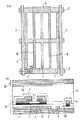
(Embodiment 2)
FIG. 2A schematically shows a planar configuration of a pixel portion of the array substrate according to (Embodiment 2) of the present invention, and FIG. 2B is a liquid crystal display device taken along one-dot chain line in FIG. The schematic sectional drawing of this sectional structure is shown. Descriptions of parts common to those in the first embodiment are omitted, and different parts are described.
[0029]
(Embodiment 2), after pattern formation of the
[0030]
Further, aluminum (Al) was deposited, and the
[0031]
【The invention's effect】
As described above, the active matrix liquid crystal display device of the present invention is such that the film thickness of the pixel electrode is made thinner than that of the signal wiring in the IPS liquid crystal display device capable of realizing good multi-gradation display with a wide viewing angle. a simple structure, or to reduce the tolerance for the disconnection failure and without or increasing the wiring resistance, can omission nonoriented light in the vicinity of the pixel electrodes in prevention, it is possible to obtain a highly contrast image .
[Brief description of the drawings]
FIG. 1 is a plan view and a cross-sectional view schematically showing a planar configuration of a pixel portion of an array substrate in an active matrix liquid crystal display device according to (Embodiment 1) of the present invention. FIG. 3 is a plan view and a cross-sectional view schematically showing the planar configuration of the pixel portion of the array substrate in the active matrix liquid crystal display device of FIG. Plan view and cross-sectional view [Explanation of symbols]
DESCRIPTION OF
12
Claims (4)
前記アレイ基板に対向して配置された対向基板と、
前記アレイ基板と前記対向基板との間に挟持された液晶層とを具備し、
前記液晶層に、前記アレイ基板に対してほぼ平行な方向の電界が印加されるアクティブマトリクス型液晶表示装置であって、
前記信号配線は複数層から成り、前記画素電極が前記複数層の最上層を除いた層から形成されることにより、前記画素電極の膜厚が前記信号配線の膜厚より薄いこと
を特徴とするアクティブマトリクス型液晶表示装置。A plurality of signal wirings and scanning wirings arranged in a matrix, one or more switching elements provided at each intersection of the signal wirings and scanning wirings, a pixel electrode connected to the switching elements, and the pixels An array substrate having a common electrode formed by occlusion with the electrode, and an alignment film subjected to rubbing treatment;
A counter substrate disposed to face the array substrate;
A liquid crystal layer sandwiched between the array substrate and the counter substrate;
An active matrix liquid crystal display device in which an electric field in a direction substantially parallel to the array substrate is applied to the liquid crystal layer,
The signal wiring includes a plurality of layers, and the pixel electrode is formed of a layer excluding the uppermost layer of the plurality of layers, so that the film thickness of the pixel electrode is smaller than the film thickness of the signal wiring. Active matrix liquid crystal display device.
を特徴とする請求項1または請求項2記載のアクティブマトリクス型液晶表示装置。3. The active matrix type according to claim 1, wherein the outermost surface of the pixel electrode is formed of a conductive material having a reflectance lower than that of aluminum, or the pixel electrode is formed of a transparent conductive material. Liquid crystal display device.
を特徴とする請求項1〜請求項3のいずれか1項に記載のアクティブマトリクス型液晶表示装置。4. The device according to claim 1, wherein at least a part of the signal wiring and the pixel electrode are formed on the same film so as to be in contact with the film. 5. Active matrix liquid crystal display device.
Priority Applications (1)
| Application Number | Priority Date | Filing Date | Title |
|---|---|---|---|
| JP6713397A JP4036498B2 (en) | 1997-03-21 | 1997-03-21 | Active matrix liquid crystal display device |
Applications Claiming Priority (1)
| Application Number | Priority Date | Filing Date | Title |
|---|---|---|---|
| JP6713397A JP4036498B2 (en) | 1997-03-21 | 1997-03-21 | Active matrix liquid crystal display device |
Related Child Applications (1)
| Application Number | Title | Priority Date | Filing Date |
|---|---|---|---|
| JP2004347926A Division JP4215708B2 (en) | 2004-12-01 | 2004-12-01 | Active matrix liquid crystal display device |
Publications (2)
| Publication Number | Publication Date |
|---|---|
| JPH10260431A JPH10260431A (en) | 1998-09-29 |
| JP4036498B2 true JP4036498B2 (en) | 2008-01-23 |
Family
ID=13336105
Family Applications (1)
| Application Number | Title | Priority Date | Filing Date |
|---|---|---|---|
| JP6713397A Expired - Fee Related JP4036498B2 (en) | 1997-03-21 | 1997-03-21 | Active matrix liquid crystal display device |
Country Status (1)
| Country | Link |
|---|---|
| JP (1) | JP4036498B2 (en) |
Families Citing this family (15)
| Publication number | Priority date | Publication date | Assignee | Title |
|---|---|---|---|---|
| KR100306799B1 (en) | 1998-05-29 | 2001-11-30 | 박종섭 | Liquid crystal display |
| KR100306800B1 (en) | 1998-05-29 | 2002-06-20 | 박종섭 | Liquid crystal display and method for fabricating the same |
| KR100621857B1 (en) * | 1999-03-19 | 2006-09-12 | 엘지.필립스 엘시디 주식회사 | Liquid crystal display |
| KR100303448B1 (en) * | 1999-04-26 | 2001-10-29 | 윤종용 | a liquid crystal display and a manufacturing method thereof |
| KR100311212B1 (en) * | 1999-06-29 | 2001-11-02 | 박종섭 | LCD having high aperture ratio and high transmittance |
| KR100607145B1 (en) * | 2000-02-11 | 2006-08-01 | 엘지.필립스 엘시디 주식회사 | Transverse electric field liquid crystal display device |
| JP2001264810A (en) * | 2000-03-21 | 2001-09-26 | Nec Kagoshima Ltd | Active matrix substrate and method of manufacturing the same |
| JP4795555B2 (en) * | 2001-03-30 | 2011-10-19 | 東芝モバイルディスプレイ株式会社 | Manufacturing method of image display device |
| JP3774858B2 (en) * | 2001-04-07 | 2006-05-17 | 大林精工株式会社 | Liquid crystal display device and driving method thereof |
| JP3586674B2 (en) | 2002-01-30 | 2004-11-10 | Nec液晶テクノロジー株式会社 | Liquid crystal display |
| JP2003228081A (en) | 2002-01-31 | 2003-08-15 | Nec Corp | Liquid crystal display device and manufacturing method therefor |
| KR100595453B1 (en) * | 2003-11-29 | 2006-06-30 | 엘지.필립스 엘시디 주식회사 | Horizontal field type liquid crystal display device |
| JP2005283870A (en) * | 2004-03-29 | 2005-10-13 | International Display Technology Kk | Image display device |
| JP5553513B2 (en) * | 2009-02-09 | 2014-07-16 | 株式会社ジャパンディスプレイ | Liquid crystal display device and manufacturing method thereof |
| CN105826328B (en) * | 2016-05-03 | 2019-03-05 | 京东方科技集团股份有限公司 | Array substrate, method for manufacturing the same, and display device |
-
1997
- 1997-03-21 JP JP6713397A patent/JP4036498B2/en not_active Expired - Fee Related
Also Published As
| Publication number | Publication date |
|---|---|
| JPH10260431A (en) | 1998-09-29 |
Similar Documents
| Publication | Publication Date | Title |
|---|---|---|
| KR100246980B1 (en) | Active matrix type liquid crystal display elements | |
| JP2859093B2 (en) | Liquid crystal display | |
| JP4002105B2 (en) | Liquid crystal display | |
| US20050200791A1 (en) | In-plane switching mode liquid crystal display device and fabrication method thereof | |
| JPH11242238A (en) | Reflection type liquid crystal display device, method for manufacturing the same, and method for manufacturing circuit board | |
| JP4036498B2 (en) | Active matrix liquid crystal display device | |
| US6570638B2 (en) | Liquid crystal display including pixel electrodes with plurality of openings | |
| JP2002182230A (en) | Fringe field switching mode liquid crystal display | |
| JP3646999B2 (en) | Transmission type liquid crystal display device | |
| US7724325B2 (en) | Liquid crystal display device and method for manufacturing the same | |
| US20100244035A1 (en) | Display panel and method of forming thereof | |
| JP3204912B2 (en) | Active matrix liquid crystal display | |
| US20060001814A1 (en) | In-plane switching mode liquid crystal display device and fabricating method thereof | |
| JP3795235B2 (en) | Active matrix type liquid crystal display device | |
| US6583841B2 (en) | In-Plane switching LCD panel wherein pixel electrodes and common electrodes having plurality of first tips and second tips respectively | |
| JPH10333180A (en) | Liquid crystal display device | |
| JPH0954341A (en) | Active matrix liquid crystal display device | |
| JP3199221B2 (en) | Liquid crystal display device and manufacturing method thereof | |
| JP4813550B2 (en) | Display device | |
| JP2007206557A (en) | Liquid crystal display device | |
| JP4166554B2 (en) | Liquid crystal display device and manufacturing method thereof | |
| JP4215708B2 (en) | Active matrix liquid crystal display device | |
| JP3164987B2 (en) | Active matrix type liquid crystal display | |
| JP2000250056A (en) | Liquid crystal display and electronic equipment | |
| JP3759426B2 (en) | Liquid crystal display element |
Legal Events
| Date | Code | Title | Description |
|---|---|---|---|
| A02 | Decision of refusal |
Free format text: JAPANESE INTERMEDIATE CODE: A02 Effective date: 20041005 |
|
| A521 | Written amendment |
Free format text: JAPANESE INTERMEDIATE CODE: A523 Effective date: 20041201 |
|
| A911 | Transfer of reconsideration by examiner before appeal (zenchi) |
Free format text: JAPANESE INTERMEDIATE CODE: A911 Effective date: 20041209 |
|
| A912 | Removal of reconsideration by examiner before appeal (zenchi) |
Free format text: JAPANESE INTERMEDIATE CODE: A912 Effective date: 20050114 |
|
| A521 | Written amendment |
Free format text: JAPANESE INTERMEDIATE CODE: A523 Effective date: 20070723 |
|
| A521 | Written amendment |
Free format text: JAPANESE INTERMEDIATE CODE: A523 Effective date: 20070903 |
|
| A61 | First payment of annual fees (during grant procedure) |
Free format text: JAPANESE INTERMEDIATE CODE: A61 Effective date: 20071030 |
|
| FPAY | Renewal fee payment (prs date is renewal date of database) |
Free format text: PAYMENT UNTIL: 20101109 Year of fee payment: 3 |
|
| FPAY | Renewal fee payment (prs date is renewal date of database) |
Free format text: PAYMENT UNTIL: 20111109 Year of fee payment: 4 |
|
| FPAY | Renewal fee payment (prs date is renewal date of database) |
Free format text: PAYMENT UNTIL: 20121109 Year of fee payment: 5 |
|
| FPAY | Renewal fee payment (prs date is renewal date of database) |
Free format text: PAYMENT UNTIL: 20131109 Year of fee payment: 6 |
|
| FPAY | Renewal fee payment (prs date is renewal date of database) |
Free format text: PAYMENT UNTIL: 20131109 Year of fee payment: 6 |
|
| FPAY | Renewal fee payment (prs date is renewal date of database) |
Free format text: PAYMENT UNTIL: 20141109 Year of fee payment: 7 |
|
| S533 | Written request for registration of change of name |
Free format text: JAPANESE INTERMEDIATE CODE: R313533 |
|
| R350 | Written notification of registration of transfer |
Free format text: JAPANESE INTERMEDIATE CODE: R350 |
|
| S111 | Request for change of ownership or part of ownership |
Free format text: JAPANESE INTERMEDIATE CODE: R313113 |
|
| R350 | Written notification of registration of transfer |
Free format text: JAPANESE INTERMEDIATE CODE: R350 |
|
| LAPS | Cancellation because of no payment of annual fees |