JP4031628B2 - Semiconductor multilayer crystal, light-emitting element using the same, and method for growing the semiconductor multilayer crystal - Google Patents
Semiconductor multilayer crystal, light-emitting element using the same, and method for growing the semiconductor multilayer crystal Download PDFInfo
- Publication number
- JP4031628B2 JP4031628B2 JP2001307452A JP2001307452A JP4031628B2 JP 4031628 B2 JP4031628 B2 JP 4031628B2 JP 2001307452 A JP2001307452 A JP 2001307452A JP 2001307452 A JP2001307452 A JP 2001307452A JP 4031628 B2 JP4031628 B2 JP 4031628B2
- Authority
- JP
- Japan
- Prior art keywords
- plane
- crystal
- substrate
- semiconductor multilayer
- gallium nitride
- Prior art date
- Legal status (The legal status is an assumption and is not a legal conclusion. Google has not performed a legal analysis and makes no representation as to the accuracy of the status listed.)
- Expired - Fee Related
Links
Images


Landscapes
- Crystals, And After-Treatments Of Crystals (AREA)
Description
【0001】
【発明の属する技術分野】
本発明は、ウルツ鉱型の結晶構造を持つ半導体多層膜結晶、およびそれを用いた発光素子、ならびに当該半導体多層膜結晶の成長方法に関する。
【0002】
【従来の技術】
従来のウルツ鉱型の結晶構造を持つ半導体基板(以下、ウルツァイト型基板と略称する。)の製造方法には、以下のようなものが知られている。
【0003】
まず、サファイア(Al2O3)からなる基板上に、窒化ガリウム(GaN)からなる結晶層を形成する構成が報告されている(S.Nakamura:J.Vac.Sci.Technol.A,Vol.13,No.3,P.705,May/Jun 1995)(以下、第1の従来例と呼ぶ)。この場合、図6(a)に示すように、窒化ガリウムからなる結晶層の表面には、面方位の(0001)面(=c面)が現われる。
【0004】
一方、図6(b)に示すように、主面の面方位が(0001)面以外の面方位を持つ窒化ガリウムからなる結晶層の成長方法が、特許第2743901号公報(以下、第2の従来例と呼ぶ)に開示されている。該公報には、閃亜鉛鉱(ジンクブレンド)型の結晶構造を持つ砒化ガリウム(GaAs)からなる基板における、(001)面を基準として傾斜角が0°を越えて35°未満である主面上に、窒化ガリウムからなる半導体結晶を成長させることを記載している。なお、成長した窒化ガリウム結晶層の表面の面方位は教示されていない。
【0005】
また、特開平10−190059号公報(以下、第3の従来例と呼ぶ)には、III 族元素の原料に塩化物を用いた気相成長法を用いて、主面の面方位が(100)面の砒化ガリウムからなる基板上、又は(100)面から15°以内で傾斜した主面を持つ傾斜基板上に窒化ガリウム系半導体を成長すると、c軸が砒化ガリウム基板の[111]方向に向いたウルツァイト型の良質な窒化ガリウム系半導体層が成長することを開示している。この窒化ガリウム系半導体層のc軸は基板面に垂直な方向から55°程度傾いており、そのへき開面は基板面に垂直な(11−20)面であることを開示している。なお、ここでも、成長した窒化ガリウム結晶層の表面の面方位は教示されていない。
【0006】
【発明が解決しようとする課題】
しかしながら、前記第1の従来例は、サファイア基板上に成長した窒化ガリウム結晶層の表面は(0001)面であり、さらに六方柱状晶を含む構成となっている。すなわち、窒化ガリウム結晶層は、実質的に多数のコラム型結晶の集合体となっている。その結果、柱状晶の一部が各c軸を中心に回転して格子欠陥を生じ、結晶性が劣化するという問題がある。また、各柱状晶ごとに結晶の成長速度が異なるため、平坦な表面を得ることができないという問題がある。
【0007】
さらに、第1の従来例において、気相成長法により結晶成長を行なう場合には、結晶表面がガリウム面となる。これは、閃亜鉛鉱型の砒化ガリウムにおいては(111)A面に相当する。一般に、砒化ガリウムの(111)A面は結晶成長が困難であり、特に2次元成長が困難である。また、(111)A面にエッチングを行なったとしても、平坦なエッチングがされにくいという問題がある。これは、エッチングレートが遅いため、エッチングレートが速い他の面がエッチングされてしまい、その結果、エッチング面が凹凸状となるためである。これは、窒化ガリウムの(0001)面に対してウエットエッチングを行なった場合に、エッチピット付近が激しくエッチングされて凹凸状を呈することと良く符合する。
【0008】
一方、第3の従来例においては、砒化ガリウムからなる基板上に成長した窒化ガリウムは格子定数の差による歪の影響により、c軸の方向が5°程度傾き、さらには、六方柱状晶も回転して、格子欠陥が導入される。従って、第3の従来例に係る成長方法は、窒化ガリウムのc軸が基板面に垂直な方向から55°傾いていても、種々の面方位の微結晶によりその表面が形成されてしまうという問題がある。
【0009】
また、ウルツァイト型の単結晶体を形成する炭化珪素(SiC)においても、その表面の面方位には(0001)面を用いている。
【0010】
本発明は、前記従来の問題を解決し、基板主面の平坦性が向上し、特に柱状晶(コラム)を含まないウルツァイト型基板を形成できるようにすることを目的とする。
【0011】
【課題を解決するための手段】
前記の目的を達成するため、本発明は、ウルツァイト型基板の主面に、閃亜鉛鉱型結晶からなる基板の主面に通常用いられる(001)面とほぼ等価な面である(10−12)面を用いる構成とする。なお、本願明細書においては、結晶面を表わすミラー指数における負符号”−”は該符号に続く一の指数の反転値を表わしている。
【0012】
具体的には、本発明に係る半導体多層膜結晶は、窒化ガリウム基板および前記窒化ガリウム基板上に成長した(10−12)面を主面とする半導体多層膜よりなり、前記半導体多層膜はガリウム、アルミニウム及びインジウムのうちの少なくとも1つを III 族元素とする III- V族窒化物半導体結晶よりなり、前記窒化ガリウム基板の表面は(10−12)面である。
【0013】
本発明の半導体基板によると、面方位が(0001)面から晶帯軸の<10−10>方向に約45°〜約65°傾いた(10−12)面は、後述するように、砒化ガリウムのような閃亜鉛鉱型の結晶構造の(001)面とほぼ等価な面となる。この(001)面は、六方柱状晶とならないため、結晶表面の平坦化を図ることができ、さらにはエッチング面も平坦となる。
【0014】
また、半導体基板を構成する2元素をAXとすると、基板面に第1の元素Aのみが現わるA面、又は第2の元素Xのみが現われるB面のように、特定の極性を示す面方位が現われないため、基板上に成長する結晶層の品質が良好となり、また、基板に対するエッチング面の平坦化を図ることができる。
【0016】
本発明の半導体基板において、主面の面方位が晶帯軸の<1−210>方向におよそ−10°〜+10°の範囲で傾斜していることが好ましい。ウルツァイト型結晶構造の(10−12)面は、閃亜鉛鉱型結晶構造の(001)面と完全には等価な結晶面とならないため、このように主面の面方位を晶帯軸の<1−210>方向におよそ−10°〜+10°の範囲で傾斜させて調整を行なうと、基板を構成する結晶品質が向上する。
【0018】
本発明の半導体基板において、半導体基板には柱状晶が存在しないことが好ましい。
【0020】
本発明に係る半導体多層膜結晶の製造方法は、窒化ガリウム基板を、(0001)面から<10−10>方向に55度の角度に傾斜してなる(10−12)面を中心に、45度から65度の角度でスライスする工程と、燐酸あるいは硫酸を含む溶液でスライス後の前記窒化ガリウム基板表面をエッチングする工程と、前記窒化ガリウム基板の表面に気相成長法により(10−12)面を主面とする半導体多層膜を成長する工程とを有し、前記半導体多層膜はガリウム、アルミニウム及びインジウムのうちの少なくとも1つを III 族元素とする III- V族窒化物半導体結晶よりなる。
【0021】
本発明の半導体基板の製造方法によると、基板の主面の面方位を(0001)面から晶帯軸の<10−10>方向に約45°〜約65°傾けて形成するため、本発明の半導体基板を得ることができる。
【0033】
本発明に係る半導体多層膜結晶を用いた発光素子も本発明の趣旨に含まれる。
【0047】
【発明の実施の形態】
(第1の実施形態)
本発明の第1の実施形態について図面を参照しながら説明する。
【0048】
従来、図6(a)に示すように、例えば窒化ガリウム(GaN)のようなウルツァイト型の結晶構造を持つウルツァイト型基板上に、III-V族化合物半導体を結晶成長させる場合に、面方位が(0001)面となる主面を持つウルツァイト型基板を用いている。前述したように、(0001)面を主面とするウルツァイト型基板上に成長した場合には、結晶中に柱状晶を含むため、図6(b)に示す閃亜鉛鉱型の結晶構造における(001)面上に結晶成長させる場合のような良好な結晶品質を得ることができない。
【0049】
そこで、本願発明者らは、ウルツァイト型結晶構造について種々の検討を重ねた結果、以下のような知見を得ている。
【0050】
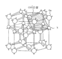
すなわち、図1に示すように、ウルツァイト型結晶構造における面方位の(10−12)面は、図2に示す閃亜鉛鉱型の結晶構造における(001)面とほぼ等価な面であるという知見である。
【0051】
従って、主面の面方位が、閃亜鉛鉱型結晶構造の(001)面とほぼ等価な面である(10−12)面を持つウルツァイト型基板の上に、ウルツァイト型の結晶構造の半導体結晶を成長させると、閃亜鉛鉱型結晶構造を持つ砒化ガリウム(GaAs)の場合と同様に、平坦な表面を容易に且つ確実に得ることができる。
【0052】
また、例えば、窒化ガリウムからなるウルツァイト型基板に対してエッチングを行なったとしても、その主面が閃亜鉛鉱型の(001)面とほぼ等価な、特定の極性を有さない(10−12)面であるため、燐酸又は硫酸を用いたウエットエッチングにより、平坦なエッチング面を得ることができる。
【0053】
図3はウルツァイト型結晶構造における(10−12)面が(0001)面に対して傾斜する傾斜角θと、傾斜する傾斜方向とを表わしている。図3に示すように、傾斜角θは55°であり、傾斜方向は<10−10>方向であることを確認している。
【0054】
さらに、本願発明者らは、図3に示す(10−12)面を±10°以内で傾斜させると結晶表面の平坦性が向上し、±5°以内で傾斜させるとさらに好ましいという知見を得ている。
【0055】
(10−12)面を±10°以内で傾斜させる理由は、図4に示すように、閃亜鉛鉱型結晶構造が有する面心立方格子の場合に存在するはずの原子Xが、ウルツァイト型結晶構造が有する細密充填格子の場合には存在せず、代わりに原子Yの格子位置にずれて存在するためである。
【0056】
このように、ABCABCというように、3層が規則的に積層する閃亜鉛鉱型結晶構造と、ABABというように、2層が規則的に積層するウルツァイト型結晶構造の両者の本質的な原子配置の違いにより、閃亜鉛鉱型結晶構造における(001)面と、ウルツァイト型結晶構造における(10−12)面とが完全に等価な面とはならない。
【0057】
このため、ウルツァイト型結晶構造における、閃亜鉛鉱型結晶構造の(001)面と等価な面は(10−12)面から±5°以内の範囲でずれることになる。従って、ウルツァイト型基板において、その主面の面方位を(10−12)面から±5°以内で傾斜させると、閃亜鉛鉱型結晶構造の(001)面と極めて近い面方位を持たせることができる。
【0058】
なお、ウルツァイト型結晶構造における(10−12)面においては、閃亜鉛鉱型結晶構造における<110>方向と等価な方向が<1−210>方向となるため、該<1−210>方向に±10°以内の方向で傾斜させてもよい。さらに、閃亜鉛鉱型結晶構造における<100>方向と等価な<3−30−2>方向に±10°以内で傾斜させてもよい。
【0061】
(ウルツァイト型基板の第1の製造方法)
以下、前記のように構成されたウルツァイト型基板の第1の製造方法について説明する。
【0062】
まず、引き上げ方向を<0001>(=c軸)方向とする、5mm角の種結晶を用意する。この種結晶には格子欠陥が導入されておらず、また不純物がドープされていないアンドープの結晶片を用いる。
【0063】
次に、約4万気圧で且つ温度が約2500℃の窒素雰囲気で、窒化ガリウムを溶融し、用意した種結晶を用いて窒化ガリウムからなる単結晶体をc軸方向に引き上げる。
【0064】
次に、形成された結晶体から、(0001)(=c)面から<10−10>方向に約45°〜65°の角度で、より好ましくは約50°〜60°の角度でスライスすることにより、(10−12)面又はその近傍面を主面とする窒化ガリウムからなるウエハを形成する。
【0065】
なお、ここで、晶帯軸の<10−12>方向を引き上げ方向とする種結晶を用いてもよい。この場合には、(10−12)面を、引き上げ方向に対して垂直にスライスすることにより、切り出すことが可能となるため、窒化ガリウムからなるウエハの大口径化を図ることができる。
【0066】
次に、形成されたウエハの表面を研磨によりほぼ鏡面状にして、その後、燐酸、硫酸又はこれらの混合溶液によりさらに平坦な鏡面状になるようにエッチングを行なう。
【0067】
このように、第1の製造方法によると、窒化ガリウムからなる単結晶体を引き上げ法により形成するため、単結晶体には、原理的に柱状晶が含まれることがない。さらに、ウルツァイト型結晶構造を持つ単結晶体から、そのc面から<10−10>方向に約55°の角度でスライスして、閃亜鉛鉱型結晶構造の(001)面と極めて近い面方位に相当する(10−12)面又はその近傍面を切り出してウエハ主面を形成する。このため、該ウエハの主面に対してウエットエッチングを行なったとしても、エッチング表面が凹凸状となることはなく、鏡面状態を維持することができる。
【0068】
なお、単結晶体の引き上げ時に、窒化ガリウムの溶融体中にアルミニウムを添加しておくと、窒化アルミニウムガリウム(AlGaN)からなる単結晶体を引き上げることができる。また、アルミニウム(Al)及びボロン(B)を添加しておくことにより、窒化ボロンアルミニウムガリウム(BAlGaN)からなる単結晶体を引き上げることができる。
【0069】
(結晶成長方法)
さらに、第1の実施形態に係るウルツァイト型基板上に、III-V族窒化物半導体結晶を成長させる場合には、再度、燐酸、硫酸又はこれらの混合溶液により、ウエハ表面に対してエッチング洗浄を行なって、表面を10nm程度の厚さ分だけ除去することにより、ウエハを清浄化する。
【0070】
次に、例えば、エッチング清浄されたウルツァイト型基板を反応室に投入し、有機金属気相成長(MOVPE)法により、該ウルツァイト型基板をアンモニア雰囲気中で900℃程度にまで昇温する。
【0071】
次に、基板温度を1000℃程度にまで連続的に昇温し、例えば、ガリウム(Ga)、アルミニウム(Al)及びインジウム(In)のうちの少なくとも1つをIII 族源とし、アンモニア(NH3 )をV族源としてIII-V族窒化物半導体結晶を成長する。
【0072】
ここで、成長する半導体結晶の導電型をn型とする場合には、珪素(Si)、スズ(Sn)、酸素(O)を不純物としてドーピングする。また、導電型をp型とする場合には、マグネシウム(Mg)、亜鉛(Zn)、ベリリウム(Be)又はカルシウム(Ca)を不純物としてドーピングする。
【0073】
(ウルツァイト型基板の第2の製造方法)
以下、第1の実施形態に係るウルツァイト型基板を炭化珪素により形成する場合の第2の製造方法について説明する。
【0074】
まず、引き上げ方向を<0001>(=c軸)方向とする、5mm角の種結晶を用意する。この種結晶には格子欠陥が導入されておらず、また不純物がドープされていないアンドープの結晶片を用いる。
【0075】
次に、約10万気圧で且つ温度が約3200℃のシリコン雰囲気で、炭化珪素を溶融し、用意した種結晶を用いて炭化珪素からなる単結晶体をc軸方向に引き上げる。
【0076】
次に、形成された結晶体から、(0001)面から<10−10>方向に約45°〜65°の角度で、より好ましくは約50°〜60°の角度でスライスすることにより、(10−12)面又はその近傍面を基板主面とする炭化珪素からなるウエハを形成する。
【0077】
なお、ここでも、晶帯軸の<10−12>方向を引き上げ方向とする種結晶を用いてもよい。前述したように、この場合には、(10−12)面を、引き上げ方向に対して垂直にスライスすることにより、切り出すことが可能となるので、炭化珪素からなるウエハの大口径化を図ることができる。
【0078】
次に、形成されたウエハの表面を研磨によりほぼ鏡面状にして、その後、フッ酸、硝酸又はこれらの混合溶液によりさらに鏡面状にエッチングする。
【0079】
このように、第2の製造方法によると、炭化珪素からなる単結晶体を引き上げ法により形成するため、単結晶体には、原理的に柱状晶が含まれることがない。さらに、ウルツァイト型結晶構造を持つ単結晶体から、そのc面から<10−10>方向に約55°の角度でスライスして、閃亜鉛鉱型結晶構造の(001)面と極めて近い面方位である(10−12)面又はその近傍面を切り出してウエハ主面を形成する。このため、該ウエハの主面に対してウエットエッチングを行なったとしても、エッチング表面が凹凸状となることはなく、鏡面状態を維持することができる。
【0080】
(結晶成長方法)
形成した炭化珪素からなる半導体基板を、結晶成長前にフッ酸、硝酸又はこれらの混合溶液により、ウエハ表面に対してエッチング洗浄を行なって、表面を10nm程度の厚さ分だけ除去することにより、ウエハを清浄化する。
【0081】
次に、例えば、エッチング清浄された半導体基板を反応室に投入し、MOVPE法により、該ウルツァイト型基板をアンモニア雰囲気中で900℃程度にまで昇温する。
【0082】
次に、基板温度を1000℃程度にまで連続的に昇温し、例えば、ガリウム、アルミニウム及びインジウムのうちの少なくとも1つをIII 族源とし、アンモニアをV族源としてIII-V族窒化物半導体結晶を成長する。
【0083】
(第2の実施形態)
以下、本発明の第2の実施形態に係るウルツァイト型基板の製造方法について説明する。
【0084】
まず、図6(a)に示すように、従来と同様に、昇華法又はMOVPE法等の気相成長法を用いて、主面が(001)面のサファイア基板上に、例えば窒化ガリウムからなり、表面の面方位が(0001)であり、少なくとも膜厚が5mm以上の第1の結晶層を成長する。
【0085】
次に、図3に示すように、成長した第1の結晶層における(001)面から<10−10>方向に約55°の角度で、閃亜鉛鉱型結晶構造の(001)面と極めて近い面方位である(10−12)面又はこの面に対して±10°以内の面が主面となるようにスライスする。
【0086】
次に、形成した主面上に気相成長法により、厚さが約2μmの窒化ガリウムからなる第2の結晶層を成長して、主面が(10−12)面又はこれに近い面方位を持つウルツァイト型基板を形成する。
【0087】
なお、第2の実施形態の場合には、第1の結晶層中に六方晶の回転が存在しているため、柱状晶を完全になくすことはできない。
【0088】
(第3の実施形態)
以下、本発明の第3の実施形態について図面を参照しながら説明する。
【0089】
図5(a)〜図5(c)は本発明の第3の実施形態に係る半導体レーザ素子であって、(a)は半導体レーザ素子を形成する半導体基板の主面の面方位を表わす結晶格子を表わし、(b)は半導体レーザ素子における共振器の形成方向を表わし、(c)は半導体レーザ素子における共振器の他の形成方向を表わしている。
【0090】
まず、従来の共振器の形成方向を説明する。
【0091】
図7(a)に示すように、従来は、主面の面方位が(0001)面であるウルツァイト型基板上に、レーザ発振用の共振器を形成しているため、共振器における共振方向(レーザ発振方向)、いわゆるストライプ方向は、符号51が示す<11−20>方向、又は符号52が示す<1−100>方向である。
【0092】
一方、図7(b)に示す閃亜鉛鉱型の結晶構造を持つ半導体基板の場合には、前述したように、その主面の面方位は、一般に(001)面であり、ストライプ方向は、符号53が示す<110>方向、又は符号54が示す<1−10>方向である。
【0093】
このことから、半導体レーザ素子を、面方位が(10−12)面であるウルツァイト型基板上に形成する場合には、図5(b)に示すように、符号11が示す<1−210>方向、又は図5(c)に示すように、符号12が示す<2−1−1−2>方向を選択することが好ましいことが分かる。
【0094】
このように、共振器端面に(1−210)面又は(2−1−1−2)面を持つ共振器構造を形成すると、対向する端面同士のへき開面が互いに平行で且つ平坦となる共振器として確実に機能する。
【0095】
これにより、共振器構造の加工性が良好となる上に、発光効率が向上して、長期信頼性を得られるようになる。
【0096】
以下、第3の実施形態に係る半導体レーザ素子の製造方法について説明する。
【0097】
まず、第1の実施形態又は第2の実施形態に係る製造方法により得られた半導体基板、すなわち、主面の面方位が(10−12)面又は該(10−12)面から<10−10>方向に±10°以内で傾斜させた窒化ガリウムからなるウルツァイト型基板を用意する。
【0098】
次に、燐酸、硫酸又はこれらの混合溶液により、基板の主面に対してエッチング洗浄を行なって、該主面を10nm程度の厚さ分だけ除去することにより、ウルツァイト型基板の主面を清浄化する。
【0099】
次に、例えば、有機金属気相成長(MOVPE)法により、エッチング清浄されたウルツァイト型基板を反応室に投入し、該基板をアンモニア雰囲気中で900℃程度にまで昇温する。その後、基板温度を1000℃程度にまで昇温し、例えば、III 族源であるテトラメチルガリウム(TMG)及びテトラメチルアルミニウム(TMA)と、V族源であるアンモニア(NH3 )と、n型ドーパントの珪素を含むシランガスとを反応室に導入して、ウルツァイト型基板の主面上に、n型AlGaNからなる第1のクラッド層を成長する。
【0100】
次に、TMAの導入を中止して、第1のクラッド層の上に、n型GaNからなる第1の光ガイド層を成長する。
【0101】
次に、シランガスの導入を中止し、代わりにトリメチルインジウム(TMI)を導入することにより、第1の光ガイド層の上にInGaNからなる量子井戸活性層を成長する。
【0102】
次に、TMIの代わりにTMAを導入し、さらに、p型ドーパントのマグネシウムを含むビスシクロペンタジエニルマグネシウム(Cp2 Mg)を導入して、量子井戸活性層の上にp型AlGaNからなるキャップ層を成長する。
【0103】
次に、TMAの導入を中止して、キャップ層の上にp型GaNからなる第2の光ガイド層を成長する。
【0104】
次に、TMAの導入を再開して、第2の光ガイド層の上にp型AlGaNからなる第2のクラッド層を成長する。その後、TMAの導入を再度中止して、p型GaNからなるコンタクト層を成長する。
【0105】
次に、蒸着法等により、p型コンタクト層の全面に、ニッケル(Ni)、白金(Pt)及びAu(金)からなる導体膜を順次堆積して第1の積層導体膜を形成する。その後、リソグラフィ法により、レーザ光の共振方向が<1−210>方向又は<2−1−1−2>方向となるストライプパターンを持つレジストマスクを形成する。続いて、形成したレジストマスクを用いて、第1の積層導体膜、コンタクト層、第2のクラッド層及び第2の光ガイド層に対して順次ドライエッチングを行なって、上面に第1の積層導体膜からなるp側電極を有する共振器構造を形成する。その後、燐酸又は硫酸を用いて、ドライエッチングにより露出したダメージ層をエッチング除去する。
【0106】
次に、蒸着法等により、ウルツァイト型基板における主面と反対側の面上に、アルミニウム(Al)、チタン(Ti)及び金(Au)からなる第2の積層導体膜を形成してn側電極を形成する。
【0107】
次に、ウルツァイト型基板を、共振器長が300μm〜1mm程度で、且つへき開面が(1−210)面又は(2−1−1−2)面となるようにへき開して、半導体レーザ素子を得る。
【0108】
なお、インジウムを含む量子井戸活性層の成長時には、基板温度を1000℃よりも低い、例えば800℃程度としてもよい。
【0109】
また、p型AlGaNからなる第2のクラッド層を設けず、且つストライプ状の共振器を有さない構造とすることにより、発光ダイオード素子とすることもできる。
【0110】
また、半導体装置は発光素子に限られず、受光素子であっても良く、また、例えば、電界効果トランジスタ(FET)又はヘテロ接合バイポーラトランジスタ(HBT)のような能動素子であっても良い。このような能動素子の場合には、リーク電流の低減に極めて大きい効果がある。
【0112】
【発明の効果】
本発明に係るウルツ鉱型の結晶構造を持つ半導体基板によると、面方位が(0001)面から晶帯軸の<10−10>方向に約45°〜約65°傾いた面を主面に持つため、閃亜鉛鉱型の結晶構造の(001)面とほぼ等価な面となる。この(001)面とほぼ等価な面は、六方柱状晶とならないため、結晶表面の平坦化を図ることができ、さらにはエッチング面も平坦となる。
【0113】
また、本発明に係る半導体装置は、本発明の表面の平坦化に優れる半導体基板上に形成されているため、電気的又は光学的に優れた特性を持たせることができる。
【図面の簡単な説明】
【図1】本発明の第1の実施形態に係る半導体基板のウルツァイト型の結晶構造であって、基板の主面である(10−12)面を表わす模式図である。
【図2】本発明の第1の実施形態に係る半導体基板と等価な主面を持つ閃亜鉛鉱型の結晶構造であって、基板の主面である(001)面を表わす模式図である。
【図3】本発明の第1の実施形態に係る半導体基板のウルツァイト型の結晶構造であって、(10−12)面の(0001)からの傾斜方向及び傾斜角度等価な面を表わす模式図である。
【図4】本発明の第1の実施形態に係る半導体基板のウルツァイト型の結晶構造であって、(10−12)面と等価な面を表わす模式図である。
【図5】本発明の第3の実施形態に係る半導体レーザ素子を示し、(a)は半導体基板のウルツァイト型の結晶構造とその主面の面方位を表わす模式図であり、(b)は半導体レーザ素子の共振器における第1のストライプ方向を表わす模式図であり、(c)は半導体レーザ素子の共振器における第2のストライプ方向を表わす模式図である。
【図6】(a)は従来のウルツァイト型基板の結晶構造とその基板の主面である(0001)面を表わす模式図である。
(b)は従来の閃亜鉛鉱型基板の結晶構造とその基板の主面である(001)面を表わす模式図である。
【図7】(a)は従来のウルツァイト型基板の結晶構造とその基板の主面である(0001)面上に形成される共振器のストライプ方向を表わす模式図である。
(b)は従来の閃亜鉛鉱型基板の結晶構造とその基板の主面である(001)面上に形成される共振器のストライプ方向を表わす模式図である。
【符号の説明】
11 共振器
12 共振器[0001]
BACKGROUND OF THE INVENTION
The present invention has a wurtzite crystal structureSemiconductor multilayer crystal, light-emitting element using the same, and method for growing the semiconductor multilayer crystalAbout.
[0002]
[Prior art]
As a conventional method for manufacturing a semiconductor substrate having a wurtzite type crystal structure (hereinafter abbreviated as a wurtzite substrate), the following is known.
[0003]
First, sapphire (Al2OThree) Has been reported (S. Nakamura: J. Vac. Sci. Technol. A, Vol. 13, No. 3, P.). 705, May / Jun 1995) (hereinafter referred to as the first conventional example). In this case, as shown in FIG. 6A, a (0001) plane (= c plane) having a plane orientation appears on the surface of the crystal layer made of gallium nitride.
[0004]
On the other hand, as shown in FIG. 6B, a method for growing a crystal layer made of gallium nitride having a plane orientation other than the (0001) plane as the principal plane is disclosed in Japanese Patent No. 2743901 (hereinafter referred to as the second method). (Referred to as a conventional example). In this publication, a main surface of a substrate made of gallium arsenide (GaAs) having a zinc blende (zinc blend) type crystal structure with an inclination angle of more than 0 ° and less than 35 ° with respect to the (001) plane. Above, it is described that a semiconductor crystal made of gallium nitride is grown. The surface orientation of the surface of the grown gallium nitride crystal layer is not taught.
[0005]
Japanese Patent Laid-Open No. 10-190059 (hereinafter referred to as “third conventional example”) uses a vapor phase growth method in which chloride is used as a group III element material, and the plane orientation of the main surface is (100 When a gallium nitride based semiconductor is grown on a substrate made of gallium arsenide on the) plane or on a tilted substrate having a main surface tilted within 15 ° from the (100) plane, the c-axis is in the [111] direction of the gallium arsenide substrate. It discloses that a good wurtzite-type high-quality gallium nitride-based semiconductor layer is grown. It is disclosed that the c-axis of the gallium nitride based semiconductor layer is inclined by about 55 ° from the direction perpendicular to the substrate surface, and the cleavage plane is a (11-20) surface perpendicular to the substrate surface. Again, the orientation of the surface of the grown gallium nitride crystal layer is not taught.
[0006]
[Problems to be solved by the invention]
However, in the first conventional example, the surface of the gallium nitride crystal layer grown on the sapphire substrate is the (0001) plane, and further includes hexagonal columnar crystals. That is, the gallium nitride crystal layer is an aggregate of a large number of column-type crystals. As a result, a part of the columnar crystal rotates around each c-axis to cause a lattice defect, and there is a problem that crystallinity deteriorates. Further, there is a problem that a flat surface cannot be obtained because the growth rate of the crystal is different for each columnar crystal.
[0007]
Furthermore, in the first conventional example, when crystal growth is performed by a vapor phase growth method, the crystal surface becomes a gallium surface. This corresponds to the (111) A plane in zinc blende gallium arsenide. In general, the (111) A plane of gallium arsenide is difficult to grow crystals, and in particular, two-dimensional growth is difficult. Further, even if the (111) A plane is etched, there is a problem that flat etching is difficult to be performed. This is because the etching rate is slow and the other surface with a high etching rate is etched, resulting in the etched surface becoming uneven. This is in good agreement with the fact that when wet etching is performed on the (0001) plane of gallium nitride, the vicinity of the etch pits is intensely etched and exhibits irregularities.
[0008]
On the other hand, in the third conventional example, gallium nitride grown on a substrate made of gallium arsenide is tilted by about 5 ° in the c-axis direction due to the influence of strain due to the difference in lattice constant, and further, hexagonal columnar crystals also rotate. Thus, lattice defects are introduced. Therefore, the growth method according to the third conventional example has a problem that even if the c-axis of gallium nitride is inclined 55 ° from the direction perpendicular to the substrate surface, the surface is formed by microcrystals of various plane orientations. There is.
[0009]
Further, silicon carbide (SiC) forming a wurtzite single crystal also uses the (0001) plane as the surface orientation of the surface.
[0010]
An object of the present invention is to solve the above-mentioned conventional problems, improve the flatness of the main surface of the substrate, and particularly to form a wurtzite substrate that does not contain columnar crystals (columns).
[0011]
[Means for Solving the Problems]
In order to achieve the above object, the present invention is a surface substantially equivalent to the (001) plane that is usually used for the main surface of the wurtzite substrate and the main surface of the substrate made of zinc blende type crystal (10-12). ) Surface. In the present specification, the minus sign “−” in the Miller index representing the crystal plane represents the inverted value of one index following the sign.
[0012]
Specifically, according to the present inventionThe semiconductor multilayer crystal is composed of a gallium nitride substrate and a semiconductor multilayer film having a (10-12) plane as a main surface grown on the gallium nitride substrate, and the semiconductor multilayer film is at least one of gallium, aluminum, and indium. One III Group element III- It consists of a group V nitride semiconductor crystal, and the surface of the gallium nitride substrate is a (10-12) plane.
[0013]
According to the semiconductor substrate of the present invention, the plane orientation is inclined by about 45 ° to about 65 ° from the (0001) plane in the <10-10> direction of the zone axis.(10-12)As will be described later, the surface is substantially equivalent to the (001) surface of a zinc blende type crystal structure such as gallium arsenide. Since the (001) plane does not become a hexagonal columnar crystal, the crystal surface can be flattened, and the etched surface also becomes flat.
[0014]
Further, when two elements constituting the semiconductor substrate are AX, a surface having a specific polarity such as an A surface where only the first element A appears on the substrate surface or a B surface where only the second element X appears on the substrate surface. Since the orientation does not appear, the quality of the crystal layer grown on the substrate becomes good, and the etching surface with respect to the substrate can be flattened.
[0016]
In the semiconductor substrate of the present invention, it is preferable that the plane orientation of the main surface is inclined in the range of about −10 ° to + 10 ° in the <1-210> direction of the crystal zone axis. The (10-12) plane of the wurtzite type crystal structure is not a crystal plane that is completely equivalent to the (001) plane of the zinc blende type crystal structure. When the adjustment is performed by inclining in the range of about −10 ° to + 10 ° in the 1-210> direction, the crystal quality constituting the substrate is improved.
[0018]
In the semiconductor substrate of the present invention, it is preferable that columnar crystals do not exist in the semiconductor substrate.
[0020]
According to the present inventionA method for producing a semiconductor multilayer crystal is made of gallium nitride.Slicing the substrate at an angle of 45 to 65 degrees around the (10-12) plane inclined at an angle of 55 degrees in the <10-10> direction from the (0001) plane, and phosphoric acid or sulfuric acid After slicing with a solution containingGallium nitrideEtching the substrate surface; andGallium nitridesubstrateofBy vapor phase growth on the surfaceThe (10-12) plane is the main planeA process for growing a semiconductor multilayer film.Shi,The semiconductor multilayer film includes at least one of gallium, aluminum, and indium. III Group element III- Made of group V nitride semiconductor crystal.
[0021]
According to the method for manufacturing a semiconductor substrate of the present invention, the plane orientation of the main surface of the substrate is inclined from the (0001) plane to the <10-10> direction of the crystal zone axis by about 45 ° to about 65 °. The semiconductor substrate can be obtained.
[0033]
The present inventionA light emitting device using the semiconductor multilayer crystal according to the present invention is also included in the spirit of the present invention.
[0047]
DETAILED DESCRIPTION OF THE INVENTION
(First embodiment)
A first embodiment of the present invention will be described with reference to the drawings.
[0048]
Conventionally, as shown in FIG. 6A, when a III-V compound semiconductor crystal is grown on a wurtzite substrate having a wurtzite crystal structure such as gallium nitride (GaN), the plane orientation is A wurtzite-type substrate having a main surface that is a (0001) plane is used. As described above, when grown on a wurtzite substrate having a (0001) plane as a main surface, the crystal contains columnar crystals, and therefore, in the zinc blende crystal structure shown in FIG. Good crystal quality as in the case of crystal growth on the (001) plane cannot be obtained.
[0049]
The inventors of the present invention have obtained the following knowledge as a result of various studies on the wurtzite crystal structure.
[0050]
That is, as shown in FIG. 1, the knowledge that the (10-12) plane in the wurtzite crystal structure is substantially equivalent to the (001) plane in the zinc blende crystal structure shown in FIG. It is.
[0051]
Therefore, a semiconductor crystal having a wurtzite crystal structure is formed on a wurtzite substrate having a (10-12) plane whose plane orientation is approximately equivalent to the (001) plane of the zinc blende crystal structure. As in the case of gallium arsenide (GaAs) having a zinc blende crystal structure, a flat surface can be obtained easily and reliably.
[0052]
Further, for example, even when etching is performed on a wurtzite substrate made of gallium nitride, the main surface thereof has substantially no equivalent polarity to the (001) surface of zinc blende type (10-12). ) Surface, a flat etching surface can be obtained by wet etching using phosphoric acid or sulfuric acid.
[0053]
FIG. 3 shows an inclination angle θ at which the (10-12) plane in the wurtzite crystal structure is inclined with respect to the (0001) plane, and an inclination direction in which the (10-12) plane is inclined. As shown in FIG. 3, it is confirmed that the inclination angle θ is 55 ° and the inclination direction is the <10-10> direction.
[0054]
Furthermore, the inventors of the present application have found that the (10-12) plane shown in FIG. 3 is tilted within ± 10 °, the flatness of the crystal surface is improved, and the tilt within ± 5 ° is more preferable. ing.
[0055]
The reason why the (10-12) plane is inclined within ± 10 ° is that, as shown in FIG. 4, the atoms X that should exist in the face-centered cubic lattice of the zinc blende crystal structure are wurtzite crystals. This is because it does not exist in the case of a finely packed lattice of the structure, but instead exists at a lattice position of the atom Y.
[0056]
Thus, the essential atomic arrangement of both the zincblende crystal structure in which three layers are regularly stacked, such as ABCABC, and the wurtzite crystal structure, in which two layers are regularly stacked, such as ABAB. Therefore, the (001) plane in the zinc blende type crystal structure and the (10-12) plane in the wurtzite type crystal structure are not completely equivalent planes.
[0057]
For this reason, in the wurtzite type crystal structure, the plane equivalent to the (001) plane of the zinc blende type crystal structure deviates from the (10-12) plane within a range of ± 5 °. Therefore, when the surface orientation of the main surface of the wurtzite substrate is tilted within ± 5 ° from the (10-12) surface, the surface orientation should be very close to the (001) surface of the zinc blende crystal structure. Can do.
[0058]
In the (10-12) plane in the wurtzite crystal structure, the <110> direction equivalent to the <110> direction in the zinc blende crystal structure is the <1-210> direction. You may incline in the direction within 10 degrees. Further, it may be tilted within ± 10 ° in the <3-30-2> direction equivalent to the <100> direction in the zinc blende crystal structure.
[0061]
(First manufacturing method of wurtzite substrate)
Hereinafter, a first manufacturing method of the wurtzite substrate configured as described above will be described.
[0062]
First, a 5 mm square seed crystal having a <0001> (= c-axis) direction as a pulling direction is prepared. This seed crystal uses an undoped crystal piece in which no lattice defect is introduced and no impurity is doped.
[0063]
Next, gallium nitride is melted in a nitrogen atmosphere at about 40,000 atmospheres and a temperature of about 2500 ° C., and a single crystal body made of gallium nitride is pulled up in the c-axis direction using the prepared seed crystal.
[0064]
Next, the formed crystal is sliced from the (0001) (= c) plane in the <10-10> direction at an angle of about 45 ° to 65 °, more preferably at an angle of about 50 ° to 60 °. As a result, a wafer made of gallium nitride having the (10-12) plane or its vicinity as the main surface is formed.
[0065]
Here, a seed crystal having the <10-12> direction of the zone axis as the pulling direction may be used. In this case, since the (10-12) plane can be cut out by slicing it perpendicularly to the pulling direction, the diameter of the wafer made of gallium nitride can be increased.
[0066]
Next, the surface of the formed wafer is made substantially mirror-like by polishing, and thereafter etching is performed so that it becomes a more even mirror surface with phosphoric acid, sulfuric acid, or a mixed solution thereof.
[0067]
Thus, according to the first manufacturing method, since the single crystal made of gallium nitride is formed by the pulling method, the single crystal does not contain columnar crystals in principle. Further, a single crystal having a wurtzite crystal structure is sliced at an angle of about 55 ° in the <10-10> direction from the c-plane, and the plane orientation is very close to the (001) plane of the zinc blende crystal structure The (10-12) plane corresponding to or near the plane is cut out to form the main surface of the wafer. For this reason, even if wet etching is performed on the main surface of the wafer, the etched surface does not become uneven, and the mirror surface state can be maintained.
[0068]
When aluminum is added to a gallium nitride melt at the time of pulling up the single crystal, the single crystal made of aluminum gallium nitride (AlGaN) can be pulled up. Further, by adding aluminum (Al) and boron (B), a single crystal made of boron aluminum gallium nitride (BAlGaN) can be pulled up.
[0069]
(Crystal growth method)
Further, when a group III-V nitride semiconductor crystal is grown on the wurtzite substrate according to the first embodiment, the wafer surface is again etched and cleaned with phosphoric acid, sulfuric acid, or a mixed solution thereof. In practice, the surface is removed by a thickness of about 10 nm to clean the wafer.
[0070]
Next, for example, the etched wurtzite-type substrate is put into the reaction chamber, and the wurtzite-type substrate is heated to about 900 ° C. in an ammonia atmosphere by metal organic vapor phase epitaxy (MOVPE).
[0071]
Next, the substrate temperature is continuously raised to about 1000 ° C., for example, at least one of gallium (Ga), aluminum (Al), and indium (In) is used as a group III source, and ammonia (NHThree ) To grow a group III-V nitride semiconductor crystal.
[0072]
Here, when the conductivity type of the growing semiconductor crystal is n-type, doping is performed using silicon (Si), tin (Sn), and oxygen (O) as impurities. When the conductivity type is p-type, doping is performed using magnesium (Mg), zinc (Zn), beryllium (Be), or calcium (Ca) as impurities.
[0073]
(Second manufacturing method of wurtzite substrate)
Hereinafter, a second manufacturing method in the case where the wurtzite substrate according to the first embodiment is formed of silicon carbide will be described.
[0074]
First, a 5 mm square seed crystal having a <0001> (= c-axis) direction as a pulling direction is prepared. This seed crystal uses an undoped crystal piece in which no lattice defect is introduced and no impurity is doped.
[0075]
Next, silicon carbide is melted in a silicon atmosphere at about 100,000 atmospheres and a temperature of about 3200 ° C., and a single crystal body made of silicon carbide is pulled up in the c-axis direction using the prepared seed crystal.
[0076]
Next, by slicing the formed crystal body at an angle of about 45 ° to 65 °, more preferably an angle of about 50 ° to 60 ° in the <10-10> direction from the (0001) plane, ( 10-12) A wafer made of silicon carbide having a substrate main surface at or near its surface is formed.
[0077]
Also here, a seed crystal having the <10-12> direction of the zone axis as the pulling direction may be used. As described above, in this case, the (10-12) plane can be cut out by slicing perpendicularly to the pulling direction, so that the diameter of the silicon carbide wafer can be increased. Can do.
[0078]
Next, the surface of the formed wafer is made substantially mirror-like by polishing, and then further etched into a mirror-like shape with hydrofluoric acid, nitric acid or a mixed solution thereof.
[0079]
Thus, according to the second manufacturing method, since the single crystal made of silicon carbide is formed by the pulling method, the single crystal does not contain columnar crystals in principle. Further, a single crystal having a wurtzite crystal structure is sliced at an angle of about 55 ° in the <10-10> direction from the c-plane, and the plane orientation is very close to the (001) plane of the zinc blende crystal structure The (10-12) plane or the vicinity thereof is cut out to form the main wafer surface. For this reason, even if wet etching is performed on the main surface of the wafer, the etched surface does not become uneven, and the mirror surface state can be maintained.
[0080]
(Crystal growth method)
By performing etching cleaning on the wafer surface with hydrofluoric acid, nitric acid or a mixed solution thereof before crystal growth, the formed semiconductor substrate made of silicon carbide is removed by a thickness of about 10 nm, Clean the wafer.
[0081]
Next, for example, the etched and cleaned semiconductor substrate is put into the reaction chamber, and the wurtzite substrate is heated to about 900 ° C. in an ammonia atmosphere by the MOVPE method.
[0082]
Next, the substrate temperature is continuously raised to about 1000 ° C., and for example, at least one of gallium, aluminum and indium is used as a group III source, and ammonia is used as a group V source. Grow crystals.
[0083]
(Second Embodiment)
Hereinafter, a method for manufacturing a wurtzite substrate according to the second embodiment of the present invention will be described.
[0084]
First, as shown in FIG. 6A, as in the prior art, a main surface is made of, for example, gallium nitride on a sapphire substrate having a (001) plane using a vapor phase growth method such as a sublimation method or a MOVPE method. A first crystal layer having a surface orientation of (0001) and a thickness of at least 5 mm is grown.
[0085]
Next, as shown in FIG. 3, it is extremely different from the (001) plane of the zinc blende crystal structure at an angle of about 55 ° in the <10-10> direction from the (001) plane in the grown first crystal layer. Slicing is performed so that the (10-12) plane having a near plane orientation or a plane within ± 10 ° with respect to this plane becomes the main plane.
[0086]
Next, a second crystal layer made of gallium nitride having a thickness of about 2 μm is grown on the formed main surface by vapor phase growth, and the main surface has a (10-12) plane or a plane orientation close thereto. A wurtzite-type substrate having a structure is formed.
[0087]
In the case of the second embodiment, since the hexagonal rotation exists in the first crystal layer, the columnar crystal cannot be completely eliminated.
[0088]
(Third embodiment)
Hereinafter, a third embodiment of the present invention will be described with reference to the drawings.
[0089]
FIGS. 5A to 5C show a semiconductor laser device according to the third embodiment of the present invention, in which FIG. 5A shows a crystal representing the plane orientation of the main surface of the semiconductor substrate forming the semiconductor laser device. (B) represents the formation direction of the resonator in the semiconductor laser element, and (c) represents the other formation direction of the resonator in the semiconductor laser element.
[0090]
First, the direction in which a conventional resonator is formed will be described.
[0091]
As shown in FIG. 7 (a), since a resonator for laser oscillation is conventionally formed on a wurtzite substrate whose principal surface has a (0001) plane, the resonance direction in the resonator ( The laser oscillation direction), the so-called stripe direction, is the <11-20> direction indicated by
[0092]
On the other hand, in the case of a semiconductor substrate having a zinc blende type crystal structure shown in FIG. 7B, as described above, the plane orientation of the main surface is generally the (001) plane, and the stripe direction is The <110> direction indicated by
[0093]
Therefore, when the semiconductor laser element is formed on a wurtzite substrate whose plane orientation is the (10-12) plane, as shown in FIG. 5B, <1-210> indicated by
[0094]
As described above, when a resonator structure having the (1-210) plane or the (2-1-1-2) plane is formed on the resonator end face, the cleaved faces between the facing end faces are parallel and flat. It functions reliably as a vessel.
[0095]
As a result, the workability of the resonator structure is improved and the light emission efficiency is improved, so that long-term reliability can be obtained.
[0096]
A method for manufacturing the semiconductor laser device according to the third embodiment will be described below.
[0097]
First, the semiconductor substrate obtained by the manufacturing method according to the first embodiment or the second embodiment, that is, the plane orientation of the main surface is <10− from the (10-12) plane or the (10-12) plane. A wurtzite substrate made of gallium nitride tilted within ± 10 ° in the 10> direction is prepared.
[0098]
Next, the main surface of the wurtzite substrate is cleaned by etching cleaning the main surface of the substrate with phosphoric acid, sulfuric acid, or a mixed solution thereof, and removing the main surface by a thickness of about 10 nm. Turn into.
[0099]
Next, for example, by an organic metal vapor phase epitaxy (MOVPE) method, an etching-cleaned wurtzite substrate is put into a reaction chamber, and the substrate is heated to about 900 ° C. in an ammonia atmosphere. Thereafter, the substrate temperature is raised to about 1000 ° C., and for example, tetramethylgallium (TMG) and tetramethylaluminum (TMA) which are group III sources and ammonia (NH) which is a group V source.Three And a silane gas containing silicon of n-type dopant are introduced into the reaction chamber to grow a first cladding layer made of n-type AlGaN on the main surface of the wurtzite substrate.
[0100]
Next, the introduction of TMA is stopped, and a first light guide layer made of n-type GaN is grown on the first cladding layer.
[0101]
Next, the introduction of silane gas is stopped, and instead of trimethylindium (TMI), a quantum well active layer made of InGaN is grown on the first optical guide layer.
[0102]
Next, TMA was introduced instead of TMI, and biscyclopentadienyl magnesium (Cp2 Mg) is introduced to grow a cap layer made of p-type AlGaN on the quantum well active layer.
[0103]
Next, the introduction of TMA is stopped, and a second light guide layer made of p-type GaN is grown on the cap layer.
[0104]
Next, the introduction of TMA is resumed, and a second cladding layer made of p-type AlGaN is grown on the second light guide layer. Thereafter, the introduction of TMA is stopped again, and a contact layer made of p-type GaN is grown.
[0105]
Next, a conductive film made of nickel (Ni), platinum (Pt), and Au (gold) is sequentially deposited on the entire surface of the p-type contact layer by vapor deposition or the like to form a first laminated conductive film. Thereafter, a resist mask having a stripe pattern in which the resonance direction of the laser beam is the <1-210> direction or the <2-1-1-2> direction is formed by lithography. Subsequently, by using the formed resist mask, dry etching is sequentially performed on the first multilayer conductor film, the contact layer, the second cladding layer, and the second light guide layer, and the first multilayer conductor is formed on the upper surface. A resonator structure having a p-side electrode made of a film is formed. Thereafter, the damaged layer exposed by dry etching is removed by etching using phosphoric acid or sulfuric acid.
[0106]
Next, a second laminated conductor film made of aluminum (Al), titanium (Ti), and gold (Au) is formed on the surface opposite to the main surface of the wurtzite substrate by vapor deposition or the like to form the n side. An electrode is formed.
[0107]
Next, the wurtzite-type substrate is cleaved so that the resonator length is about 300 μm to 1 mm and the cleavage plane is the (1-210) plane or the (2-1-1-2) plane, and the semiconductor laser element Get.
[0108]
In addition, when the quantum well active layer containing indium is grown, the substrate temperature may be lower than 1000 ° C., for example, about 800 ° C.
[0109]
In addition, a light emitting diode element can be obtained by providing a structure in which the second clad layer made of p-type AlGaN is not provided and a striped resonator is not provided.
[0110]
The semiconductor device is not limited to a light emitting element, but may be a light receiving element, or may be an active element such as a field effect transistor (FET) or a heterojunction bipolar transistor (HBT). In the case of such an active element, there is an extremely large effect in reducing the leakage current.
[0112]
【The invention's effect】
According to the semiconductor substrate having a wurtzite type crystal structure according to the present invention, a plane whose plane orientation is inclined from the (0001) plane by about 45 ° to about 65 ° in the <10-10> direction of the zone axis is the main surface. Therefore, the surface is almost equivalent to the (001) plane of the zinc blende type crystal structure. Since the plane substantially equivalent to the (001) plane does not become a hexagonal columnar crystal, the crystal surface can be flattened, and the etched surface also becomes flat.
[0113]
In addition, since the semiconductor device according to the present invention is formed on the semiconductor substrate excellent in planarization of the surface of the present invention, it can have excellent electrical or optical characteristics.
[Brief description of the drawings]
FIG. 1 is a schematic diagram showing a (10-12) plane, which is a main surface of a substrate, of a wurtzite crystal structure of a semiconductor substrate according to a first embodiment of the present invention.
FIG. 2 is a schematic view showing a (001) plane that is a zinc blende type crystal structure having a principal surface equivalent to the semiconductor substrate according to the first embodiment of the present invention. .
FIG. 3 is a schematic view showing a wurtzite crystal structure of the semiconductor substrate according to the first embodiment of the present invention, and a plane equivalent to a tilt direction and a tilt angle of (10-12) plane from (0001). It is.
FIG. 4 is a schematic view showing a wurtzite crystal structure of the semiconductor substrate according to the first embodiment of the present invention, and showing a plane equivalent to the (10-12) plane.
5A and 5B show a semiconductor laser device according to a third embodiment of the present invention, in which FIG. 5A is a schematic diagram showing a wurtzite crystal structure of a semiconductor substrate and a plane orientation of a main surface thereof, and FIG. It is a schematic diagram showing the 1st stripe direction in the resonator of a semiconductor laser element, (c) is a schematic diagram showing the 2nd stripe direction in the resonator of a semiconductor laser element.
FIG. 6A is a schematic diagram showing a crystal structure of a conventional wurtzite substrate and a (0001) plane which is the main surface of the substrate.
(B) is a schematic diagram showing the crystal structure of a conventional zinc blende type substrate and the (001) plane which is the main surface of the substrate.
7A is a schematic diagram showing a crystal structure of a conventional wurtzite substrate and a stripe direction of a resonator formed on a (0001) plane which is a main surface of the substrate. FIG.
(B) is a schematic diagram showing the crystal structure of a conventional zinc blende type substrate and the stripe direction of the resonator formed on the (001) plane which is the main surface of the substrate.
[Explanation of symbols]
11 Resonator
12 Resonator
Claims (4)
燐酸あるいは硫酸を含む溶液でスライス後の前記窒化ガリウム基板表面をエッチングする工程と、
前記窒化ガリウム基板の表面に気相成長法により(10−12)面を主面とする半導体多層膜を成長する工程とを有し、
前記半導体多層膜はガリウム、アルミニウム及びインジウムのうちの少なくとも1つを III 族元素とする III- V族窒化物半導体結晶よりなる、半導体多層膜結晶の製造方法。 Slicing a gallium nitride substrate at an angle of 45 to 65 degrees around a (10-12) plane inclined at an angle of 55 degrees in the <10-10> direction from the (0001) plane;
Etching the surface of the gallium nitride substrate after slicing with a solution containing phosphoric acid or sulfuric acid;
Wherein the vapor phase growth method on the surface of the gallium nitride substrate (10-12) plane possess a step of growing a semiconductor multilayer film having a major surface,
The method for producing a semiconductor multilayer film crystal, wherein the semiconductor multilayer film is made of a group III- V nitride semiconductor crystal in which at least one of gallium, aluminum, and indium is a group III element .
Priority Applications (1)
| Application Number | Priority Date | Filing Date | Title |
|---|---|---|---|
| JP2001307452A JP4031628B2 (en) | 2001-10-03 | 2001-10-03 | Semiconductor multilayer crystal, light-emitting element using the same, and method for growing the semiconductor multilayer crystal |
Applications Claiming Priority (1)
| Application Number | Priority Date | Filing Date | Title |
|---|---|---|---|
| JP2001307452A JP4031628B2 (en) | 2001-10-03 | 2001-10-03 | Semiconductor multilayer crystal, light-emitting element using the same, and method for growing the semiconductor multilayer crystal |
Publications (3)
| Publication Number | Publication Date |
|---|---|
| JP2003112999A JP2003112999A (en) | 2003-04-18 |
| JP2003112999A5 JP2003112999A5 (en) | 2005-06-23 |
| JP4031628B2 true JP4031628B2 (en) | 2008-01-09 |
Family
ID=19126913
Family Applications (1)
| Application Number | Title | Priority Date | Filing Date |
|---|---|---|---|
| JP2001307452A Expired - Fee Related JP4031628B2 (en) | 2001-10-03 | 2001-10-03 | Semiconductor multilayer crystal, light-emitting element using the same, and method for growing the semiconductor multilayer crystal |
Country Status (1)
| Country | Link |
|---|---|
| JP (1) | JP4031628B2 (en) |
Families Citing this family (17)
| Publication number | Priority date | Publication date | Assignee | Title |
|---|---|---|---|---|
| JP2005104742A (en) * | 2003-09-26 | 2005-04-21 | Kyocera Corp | Substrate for growing single crystal and semiconductor device |
| US7846757B2 (en) * | 2005-06-01 | 2010-12-07 | The Regents Of The University Of California | Technique for the growth and fabrication of semipolar (Ga,A1,In,B)N thin films, heterostructures, and devices |
| US7220324B2 (en) * | 2005-03-10 | 2007-05-22 | The Regents Of The University Of California | Technique for the growth of planar semi-polar gallium nitride |
| JP2006052123A (en) * | 2004-07-12 | 2006-02-23 | Sumitomo Electric Ind Ltd | N-TYPE AlN CRYSTAL, N-TYPE AlGaN SOLID SOLUTION, AND METHOD FOR PRODUCING THEM |
| JP4518209B1 (en) * | 2009-09-07 | 2010-08-04 | 住友電気工業株式会社 | Group III nitride crystal substrate, group III nitride crystal substrate with epi layer, and semiconductor device and method for manufacturing the same |
| JP4277826B2 (en) | 2005-06-23 | 2009-06-10 | 住友電気工業株式会社 | Nitride crystal, nitride crystal substrate, nitride crystal substrate with epi layer, and semiconductor device and method for manufacturing the same |
| US8771552B2 (en) | 2005-06-23 | 2014-07-08 | Sumitomo Electric Industries, Ltd. | Group III nitride crystal substrate, epilayer-containing group III nitride crystal substrate, semiconductor device and method of manufacturing the same |
| US9708735B2 (en) | 2005-06-23 | 2017-07-18 | Sumitomo Electric Industries, Ltd. | Group III nitride crystal substrate, epilayer-containing group III nitride crystal substrate, semiconductor device and method of manufacturing the same |
| TWI404122B (en) * | 2005-09-09 | 2013-08-01 | Univ California | Method for enhancing growth of semi-polar (a1,in,ga,b)n via metalorganic chemical vapor deposition |
| EP1982351A4 (en) * | 2006-01-20 | 2010-10-20 | Univ California | Method for improved growth of semipolar (al,in,ga,b)n |
| US7928446B2 (en) * | 2007-07-19 | 2011-04-19 | Mitsubishi Chemical Corporation | Group III nitride semiconductor substrate and method for cleaning the same |
| KR20100067114A (en) * | 2007-09-19 | 2010-06-18 | 더 리전츠 오브 더 유니버시티 오브 캘리포니아 | Method for increasing the area of non-polar and semi-polar nitride substrates |
| JP4390007B2 (en) | 2008-04-07 | 2009-12-24 | 住友電気工業株式会社 | Group III nitride semiconductor device and epitaxial wafer |
| JP2010027924A (en) * | 2008-07-22 | 2010-02-04 | Sumitomo Electric Ind Ltd | Group iii nitride light-emitting diode |
| JP4730422B2 (en) | 2008-10-24 | 2011-07-20 | 住友電気工業株式会社 | Group III nitride semiconductor electronic device, method of fabricating group III nitride semiconductor electronic device, and group III nitride semiconductor epitaxial wafer |
| JP4375497B1 (en) * | 2009-03-11 | 2009-12-02 | 住友電気工業株式会社 | Group III nitride semiconductor device, epitaxial substrate, and method of manufacturing group III nitride semiconductor device |
| JP5120350B2 (en) * | 2009-08-24 | 2013-01-16 | 住友電気工業株式会社 | Group III nitride semiconductor device and epitaxial wafer |
-
2001
- 2001-10-03 JP JP2001307452A patent/JP4031628B2/en not_active Expired - Fee Related
Also Published As
| Publication number | Publication date |
|---|---|
| JP2003112999A (en) | 2003-04-18 |
Similar Documents
| Publication | Publication Date | Title |
|---|---|---|
| JP3898537B2 (en) | Nitride semiconductor thin film forming method and nitride semiconductor light emitting device | |
| US6455877B1 (en) | III-N compound semiconductor device | |
| JP3201475B2 (en) | Semiconductor device and method of manufacturing the same | |
| US7632695B2 (en) | Semiconductor device manufacturing method | |
| US6790279B2 (en) | Method for manufacturing group III nitride compound semiconductor and a light-emitting device using group III nitride compound semiconductor | |
| JP3139445B2 (en) | GaN-based semiconductor growth method and GaN-based semiconductor film | |
| JP4031628B2 (en) | Semiconductor multilayer crystal, light-emitting element using the same, and method for growing the semiconductor multilayer crystal | |
| TWI232596B (en) | Process for producing group III nitride compound semiconductor, group III nitride compound semiconductor element, and process for producing group III nitride compound semiconductor substrate | |
| JP3436128B2 (en) | Method for growing nitride semiconductor and nitride semiconductor device | |
| JP3153153B2 (en) | Gallium nitride based semiconductor laser and method of manufacturing the same | |
| JP3571641B2 (en) | Nitride semiconductor device | |
| JP3470623B2 (en) | Method for growing nitride III-V compound semiconductor, method for manufacturing semiconductor device, and semiconductor device | |
| JP5638198B2 (en) | Laser diode orientation on miscut substrates | |
| JP3491538B2 (en) | Method for growing nitride semiconductor and nitride semiconductor device | |
| JP3662806B2 (en) | Method for manufacturing nitride-based semiconductor layer | |
| JP4644942B2 (en) | Crystal film, crystal substrate, and method of manufacturing semiconductor device | |
| US20080246054A1 (en) | Self-supported nitride semiconductor substrate and its production method, and light-emitting nitride semiconductor device using it | |
| JP2830814B2 (en) | Crystal growth method of gallium nitride based compound semiconductor and method of manufacturing semiconductor laser | |
| JP2000223417A (en) | Growing method of semiconductor, manufacture of semiconductor substrate, and manufacture of semiconductor device | |
| JP2024079871A (en) | Non-polar and semi-polar device formation method using epitaxial lateral overgrowth | |
| JP3934320B2 (en) | GaN-based semiconductor device and manufacturing method thereof | |
| JP2001196702A (en) | Iii nitride compound semiconductor light-emitting element | |
| JP2000022283A (en) | Semiconductor element, method for manufacturing semiconductor element, and method for manufacturing semiconductor substrate | |
| JP4363415B2 (en) | Crystal film, crystal substrate and semiconductor device | |
| JP4394800B2 (en) | Nitride III-V compound semiconductor device and manufacturing method thereof |
Legal Events
| Date | Code | Title | Description |
|---|---|---|---|
| A521 | Written amendment |
Free format text: JAPANESE INTERMEDIATE CODE: A523 Effective date: 20041001 |
|
| A621 | Written request for application examination |
Free format text: JAPANESE INTERMEDIATE CODE: A621 Effective date: 20041001 |
|
| A977 | Report on retrieval |
Free format text: JAPANESE INTERMEDIATE CODE: A971007 Effective date: 20070205 |
|
| A131 | Notification of reasons for refusal |
Free format text: JAPANESE INTERMEDIATE CODE: A131 Effective date: 20070612 |
|
| A521 | Written amendment |
Free format text: JAPANESE INTERMEDIATE CODE: A523 Effective date: 20070809 |
|
| TRDD | Decision of grant or rejection written | ||
| A01 | Written decision to grant a patent or to grant a registration (utility model) |
Free format text: JAPANESE INTERMEDIATE CODE: A01 Effective date: 20070925 |
|
| A61 | First payment of annual fees (during grant procedure) |
Free format text: JAPANESE INTERMEDIATE CODE: A61 Effective date: 20071019 |
|
| R150 | Certificate of patent or registration of utility model |
Free format text: JAPANESE INTERMEDIATE CODE: R150 |
|
| FPAY | Renewal fee payment (event date is renewal date of database) |
Free format text: PAYMENT UNTIL: 20101026 Year of fee payment: 3 |
|
| FPAY | Renewal fee payment (event date is renewal date of database) |
Free format text: PAYMENT UNTIL: 20111026 Year of fee payment: 4 |
|
| FPAY | Renewal fee payment (event date is renewal date of database) |
Free format text: PAYMENT UNTIL: 20121026 Year of fee payment: 5 |
|
| FPAY | Renewal fee payment (event date is renewal date of database) |
Free format text: PAYMENT UNTIL: 20131026 Year of fee payment: 6 |
|
| LAPS | Cancellation because of no payment of annual fees |