JP4028285B2 - Oscillator - Google Patents
Oscillator Download PDFInfo
- Publication number
- JP4028285B2 JP4028285B2 JP2002115242A JP2002115242A JP4028285B2 JP 4028285 B2 JP4028285 B2 JP 4028285B2 JP 2002115242 A JP2002115242 A JP 2002115242A JP 2002115242 A JP2002115242 A JP 2002115242A JP 4028285 B2 JP4028285 B2 JP 4028285B2
- Authority
- JP
- Japan
- Prior art keywords
- amplifier
- coupled
- oscillator
- resonator
- feedback path
- Prior art date
- Legal status (The legal status is an assumption and is not a legal conclusion. Google has not performed a legal analysis and makes no representation as to the accuracy of the status listed.)
- Expired - Fee Related
Links
- 239000013078 crystal Substances 0.000 description 20
- 239000003990 capacitor Substances 0.000 description 14
- 238000010586 diagram Methods 0.000 description 13
- 230000000694 effects Effects 0.000 description 3
- 230000010355 oscillation Effects 0.000 description 3
- 239000010453 quartz Substances 0.000 description 3
- VYPSYNLAJGMNEJ-UHFFFAOYSA-N silicon dioxide Inorganic materials O=[Si]=O VYPSYNLAJGMNEJ-UHFFFAOYSA-N 0.000 description 3
- 238000005516 engineering process Methods 0.000 description 2
- 230000004048 modification Effects 0.000 description 2
- 238000012986 modification Methods 0.000 description 2
- 230000008859 change Effects 0.000 description 1
- 230000008878 coupling Effects 0.000 description 1
- 238000010168 coupling process Methods 0.000 description 1
- 238000005859 coupling reaction Methods 0.000 description 1
- 230000001939 inductive effect Effects 0.000 description 1
- 238000000034 method Methods 0.000 description 1
- 230000004044 response Effects 0.000 description 1
Images


Classifications
-
- H—ELECTRICITY
- H03—ELECTRONIC CIRCUITRY
- H03B—GENERATION OF OSCILLATIONS, DIRECTLY OR BY FREQUENCY-CHANGING, BY CIRCUITS EMPLOYING ACTIVE ELEMENTS WHICH OPERATE IN A NON-SWITCHING MANNER; GENERATION OF NOISE BY SUCH CIRCUITS
- H03B5/00—Generation of oscillations using amplifier with regenerative feedback from output to input
- H03B5/30—Generation of oscillations using amplifier with regenerative feedback from output to input with frequency-determining element being electromechanical resonator
- H03B5/32—Generation of oscillations using amplifier with regenerative feedback from output to input with frequency-determining element being electromechanical resonator being a piezoelectric resonator
- H03B5/36—Generation of oscillations using amplifier with regenerative feedback from output to input with frequency-determining element being electromechanical resonator being a piezoelectric resonator active element in amplifier being semiconductor device
-
- H—ELECTRICITY
- H03—ELECTRONIC CIRCUITRY
- H03B—GENERATION OF OSCILLATIONS, DIRECTLY OR BY FREQUENCY-CHANGING, BY CIRCUITS EMPLOYING ACTIVE ELEMENTS WHICH OPERATE IN A NON-SWITCHING MANNER; GENERATION OF NOISE BY SUCH CIRCUITS
- H03B5/00—Generation of oscillations using amplifier with regenerative feedback from output to input
- H03B5/20—Generation of oscillations using amplifier with regenerative feedback from output to input with frequency-determining element comprising resistance and either capacitance or inductance, e.g. phase-shift oscillator
- H03B5/24—Generation of oscillations using amplifier with regenerative feedback from output to input with frequency-determining element comprising resistance and either capacitance or inductance, e.g. phase-shift oscillator active element in amplifier being semiconductor device
-
- H—ELECTRICITY
- H03—ELECTRONIC CIRCUITRY
- H03B—GENERATION OF OSCILLATIONS, DIRECTLY OR BY FREQUENCY-CHANGING, BY CIRCUITS EMPLOYING ACTIVE ELEMENTS WHICH OPERATE IN A NON-SWITCHING MANNER; GENERATION OF NOISE BY SUCH CIRCUITS
- H03B5/00—Generation of oscillations using amplifier with regenerative feedback from output to input
- H03B5/30—Generation of oscillations using amplifier with regenerative feedback from output to input with frequency-determining element being electromechanical resonator
- H03B5/32—Generation of oscillations using amplifier with regenerative feedback from output to input with frequency-determining element being electromechanical resonator being a piezoelectric resonator
- H03B5/36—Generation of oscillations using amplifier with regenerative feedback from output to input with frequency-determining element being electromechanical resonator being a piezoelectric resonator active element in amplifier being semiconductor device
- H03B5/366—Generation of oscillations using amplifier with regenerative feedback from output to input with frequency-determining element being electromechanical resonator being a piezoelectric resonator active element in amplifier being semiconductor device and comprising means for varying the frequency by a variable voltage or current
- H03B5/368—Generation of oscillations using amplifier with regenerative feedback from output to input with frequency-determining element being electromechanical resonator being a piezoelectric resonator active element in amplifier being semiconductor device and comprising means for varying the frequency by a variable voltage or current the means being voltage variable capacitance diodes
Landscapes
- Oscillators With Electromechanical Resonators (AREA)
- Inductance-Capacitance Distribution Constants And Capacitance-Resistance Oscillators (AREA)
Description
【0001】
【発明の属する技術分野】
本発明は、一般に、発振器に関し、特に、演算増幅器を用い、集積回路として実施するのに好適な発振器に関する。
【0002】
【従来の技術】
ほとんどの発振器回路は、個別トランジスタの如きディスクリート素子を用いている。かかる発振器の位相ノイズ特性は、一般的には、優れている。しかし、一層少ない構成要素から成るよりコンパクトな回路が必要となる課題がある。
【0003】
他のしばしば生じる課題は、動作周波数を決定する共振器で消費されるエネルギー量を、特に水晶発振器の設計において制御することである。水晶回路は、水晶が消費するエネルギー量を、典型的には約1mWに厳密に制限しなければならない。これと同じ課題が、バラクタ・ダイオード(可変容量ダイオード)を用いたLC発振器にも生じる。このバラクタ・ダイオードの両端間の無線周波数(RF)電圧は、このダイオードへの順方向バイアスを防止するために、注意深く制限しなければならない。
【0004】
電圧同調型水晶発振器(VXCO)にも別の課題が生じる。この課題は、部品により生じる損失とボードの損失とを克服するために、同調範囲にわたる動作で、かなりの量の利得がしばしば必要となることである。いかなる損失によっても、水晶振動子と直列になる等化抵抗が生じる。充分な利得を得るためには、多数のトランジスタが必要である。その結果、設計が複雑化し、VXCO機能のために回路基板に大きな領域が必要となる。
【0005】
発振器を形成するのに用いるほとんどの集積回路は、典型的には、マイクロプロセッサ用クロック回路の形式をとる。すなわち、ロジック・ゲートの入出力(I/O)端子の結合により、発振器を構成している。これら発振器の共振回路は、典型的には、分路コンデンサ及び直列水晶振動子を用い、その後に別の分路コンデンサが接続される。
【0006】
【発明が解決しようとする課題】
共振器の電力を独立に設定でき、位相ノイズを低く又は非常に低くできる簡単な技術により、集積回路に実現可能な発振器が望まれている。
【0007】
したがって、本発明は、共振器の消費電力を独立に設定でき、出力信号内の位相ノイズが小さく、集積回路として実施するのに好適な発振器を提供するものである。
【0008】
【課題を解決するための手段】
本発明の発振器は、正入力端、負入力端、電圧信号を発生する出力端を有する増幅器(12)と;増幅器の負入力端及び基準電位の間に結合された周波数共振器(10)と;増幅器の出力端及び負入力端の間に結合され、方向が逆で並列になったダイオード・リミッタ(14)及びこのダイオード・リミッタに並列の抵抗器(R1)を有する負帰還経路(16)と;増幅器の出力端及び正入力端の間に結合された正帰還経路とを具え;増幅器の出力端から所望周波数の電圧信号を発生することを特徴とする。
【0009】
本発明は、演算増幅器を用いた発振器である。このように演算増幅器を用いることにより、周波数共振器(10)用のインピーダンス源を低くすると共に、所望周波数にて、出力電圧信号を発生する。この演算増幅器は、正帰還経路及び負帰還経路を具えており、この負帰還経路は、第1経路(14)及び第2経路(R1)を有する。この第1経路は、出力電圧信号がゼロ交差(zero crossing:ゼロ・レベルとの交差)近傍のときに、負入力端の入力インピーダンスを低い値に駆動する。また、第2経路は、出力電圧信号がゼロ交差から振動するときに、入力インピーダンスを更に小さな値に駆動する。出力端及び正帰還経路の間にフィルタを用いて、演算増幅器の正入力端からこの演算増幅器の出力における低周波数ノイズを阻止することにより、位相ノイズを最小にする。
【0010】
本発明の目的、利点及び新規な特徴は、添付図を参照した以下の詳細説明から明らかになろう。
【発明の実施の形態】
【0011】
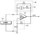
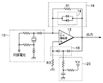
図1は、本発明による発振器の第1実施例の回路図であり、図2は、本発明による発振器の第2実施例の回路図である。これら発振器は、周波数が数十メガヘルツまでの水晶発振器又はLC発振器に有用である。これら回路は、普通の演算増幅器を用いている。メガヘルツよりも高い周波数においては、現在の帰還演算増幅器は、良好な選択である。これは、低い入力インピーダンス、典型的には約50オームのためであり、また、広い周波数応答のためでもある。図1において、増幅器(OP増幅器と図示する)12の負(−)入力端及び接地(基準電位)の間には、周波数共振器10が結合されている。増幅器12の出力端及び負入力端間には、負帰還経路16が結合されており、この負帰還経路16は、対並列(方向が逆で並列になった)ダイオード・リミッタ(振幅制限器)及び抵抗器R2が直列接続されたリミッタ14と、抵抗器R1との並列回路である。増幅器12の出力端及び正(+)入力端の間には、正帰還経路が接続されている。この正帰還経路では、陰極同士が直列接続されたダイオード・リミッタ18が増幅器12の出力端及び正入力端間に結合され、増幅器12の正入力端及び接地間には抵抗器R3が結合され、ダイオード・リミッタ18の2個のダイオードの陰極及び接地の間には、電流源20が結合されている。なお、増幅器12、正帰還経路及び負帰還経路により、演算増幅器を構成している。図2の構成は、図1と同様であるが、正帰還経路は、抵抗器R3及びR4で構成された抵抗分圧器22である。
【0012】
図1及び図2において、共振器10は、増幅器12の負入力端に入力として結合されている。共振器10は、所望周波数においてのみ、直列共振、即ち、ゼロ位相での低インピーダンスを提供する。最良の好結果となるように共振器のQを用いるために、低インピーダンスの電圧源から共振器10を駆動しなければならない。重要な点は、低インピーダンス電圧源から共振器を電圧駆動する一方、共振器10を流れる電流を用いて、この電圧源の位相を制御することである。増幅器12の負入力端及び負帰還経路16の共通接続点が共振器10の電圧源となり、共振器10からこの共通接続点側を見たインピーダンスが共振器10を駆動する電圧源のインピーダンスとなる点に留意されたい。重要な他の点は、増幅器12の負帰還経路16内に、並列抵抗器R1と共に、対並列ダイオード・リミッタ14を用いることである。
【0013】
負帰還経路16の並列抵抗器R1は、増幅器12の負入力端への充分な帰還を行い、出力電圧がほぼゼロであっても、即ち、ダイオードが開放(オフ)であっても、入力インピーダンスを小さな値に下げる。出力電圧が接地(基準電位)から振動しても、抵抗器R2及び対並列ダイオード・リミッタ14は、帰還量を増やして、入力インピーダンスを更に低い値に駆動する。対並列ダイオード・リミッタ14が導通の際、抵抗器R2を用いて、増幅器12がそれ自体のみによって発振することを防止する。帰還インピーダンスが非常に低く、共振器10の分路インピーダンスが非常に高ければ、増幅器12がVHF発振に陥るかもしれない。帯域外における分路アドミタンスが合理的な値ならば、抵抗器R2を必要ないかもしれない。
【0014】
図1において、直列のダイオード・リミッタ18は、出力信号の一部を増幅器12の正入力端に供給し、共振器10の電流と同相で、この正入力端での電圧を変化させる。抵抗器R3の値と、直列ダイオード・リミッタ18のバイアス電流(電流源20の電流)とにより、増幅器12の正入力端における電圧振動を設定する。抵抗器R1及び対並列ダイオード・リミッタ(抵抗器R2を含む)14が供給する負帰還により、増幅器12の負入力端における電圧が、正入力端における電圧と等しくなって、共振器10を低インピーダンス源から駆動する。
【0015】
最高の性能が必要ではない場合、直列ダイオード・リミッタ18を不要かもしれない。直列ダイオード・リミッタのない場合を図2に示す。この図2では、直列ダイオード・リミッタ18を簡単な抵抗分圧器22で置換している。対並列ダイオード・リミッタ14は、両方の帰還経路に対して、振幅制限機能を与える。共振器10の駆動レベル内には不確かな振幅が更にあり、抵抗性接続が回路動作において演算増幅器のオーディオ・ノイズの影響を高めており、その位相ノイズを増加させる。
【0016】
図3は、増幅器12と用いるのに適切な共振器回路10を示しており、図3Aでは、水晶振動子(XO)を増幅器12と共に用いており、図3B及び図3Cでは、電圧制御水晶発振器(VCXO)を用いている。このVCXOは、水晶振動子、バラクタ・ダイオード(可変容量ダイオード)及び抵抗器から構成されており、バラクタ・ダイオードに適切な同調電圧が供給されている。水晶共振器と共に用いる際、演算増幅器自体の発振を制御するためには、抵抗器R2が不要かもしれない。
【0017】
同様に、図4は、増幅器12と用いるのに適切な共振回路12を示している。図4Aが固定同調LC発振器用であり、インダクタ(誘導性素子)L及びコンデンサCの直列共振回路である。図4Bが電圧制御発振器(VCO)用であり、インダクタL、バイパス・コンデンサ、バラクタ・ダイオード及び抵抗器で構成されており、抵抗器を介して同調電圧がバラクタ・ダイオードに供給されている。図4BのVCO用の場合、バラクタ・ダイオード及び接地間のコンデンサがバイパスを行う。これにより、インダクタL及びバラクタ・ダイオードの間に高インピーダンス・ノードを接続する必要がなく、バラクタ・ダイオードの両端をバイアスできる。この高インピーダンス・ノードへの任意の実際的な接続により、直列共振器経路内の等化直列抵抗の形式で、信号損失が現れる。これにより、発振器のQが下がり、位相ノイズが増える。バラクタ・ダイオード及びそのバイパス・コンデンサの間の非常に低いインピーダンス点にて接続することができるので、Qを低下させることなくバラクタ・ダイオードをバイアスできると共に、小さな抵抗器を用いることにより、バラクタ・ダイオードの漏洩電流により生じるノイズ量を制限できる。このオプションは、共振器に2個のRF接続を用いる発振器回路では、しばしば利用できない。
【0018】
図5は、本発明により、水晶共振器を用いた発振器の第1実施例の実際の回路図である。図5は、図1の回路図と類似であるが、周波数共振器10及び電流源20の構成を具体的に示しており、抵抗器R2がない。共振器10では、増幅器12の負入力端と接地との間に、バラクタ・ダイオード、水晶振動子及び別のバラクタ・ダイオードの直列回路が結合されており、水晶振動子の両端には、夫々抵抗器を介して同調電圧が供給されている。電流源20は、直列ダイオード・リミッタ18と正電圧源V+との間に2個の抵抗器が直列接続されており、これら抵抗器の共通接続点と接地との間にコンデンサが結合されている。電流源20内の抵抗器が充分に大きいために、電流源として動作する。共振器10内にバラクタ・ダイオード及び水晶振動子により広帯域分路コンデンサを設けたので、リミッタ14内に抵抗器R2の必要がない。直列ダイオード・リミッタ18は、ピーク対ピークが160mVの矩形波によって、増幅器12の正入力端を駆動して、水晶共振器の損失を1mW未満に制限する。抵抗器R1による帰還経路は、演算増幅器の公称50オーム入力インピーダンスをゼロ交差において2オーム未満に下げるが、対並列ダイオード・リミッタ14が振幅制限状態にあると、2オームよりも更に下げる。これにより、水晶振動子及びバラクタ・ダイオードのループは、RFサイクルを通じて、最大のQで動作できる。バラクタ・ダイオードを同調電圧でバイアスするのに大抵抗を用いるバラクタ・バイアス回路網では、水晶振動子のループ内に挿入した直列抵抗値の観点から、水晶振動子の周囲にバラクタ・ダイオードを対称に配置する技術(水晶バラクタ技術)が最適である。
【0019】
図6は、本発明による発振器を更に変更した場合の回路図である。この回路は、図1の構成と類似しているが、ダイオード・リミッタ18と増幅器12の出力端との間にコンデンサCを有し、これらダイオード・リミッタ18及びコンデンサCの共通接続点と接地との間に第2電流源24が結合されている。電流源24の電流値は、電流源20の半分であり、その流れる方向が反対である。かかる図6での変更では、増幅器12のオーディオ周波数出力ノイズにより生じる位相ノイズを最小にしている。共振器10の具体的構成及び負帰還量に応じて、増幅器12の低周波数における利得、即ち、オーディオ利得を比較的高くできる。これは、オーディオ周波数ノイズが増幅され、このノイズが直列ダイオード・リミッタ18の入力端に現れることを意味する。図1においては、このノイズがダイオード・リミッタの入力端にてRF信号に付加されて、RF信号のゼロ交差が時間的にわずかにシフトする。これにより、位相変調がオーディオ・ノイズ、即ち、位相ノイズの関数として生じる。この影響を制限するか又はなくすためには、増幅器12の出力端及び直列ダイオード・リミッタ18の入力端の間にコンデンサCを挿入する。電流源24も追加して、直列ダイオード・リミッタ18を正確にバイアスする。コンデンサCがRF周波数にて本質的に短絡回路となり、オーディオ周波数にて開放(オフ)回路となるようにコンデンサCの大きさを選択すると、直列ダイオード・リミッタ18が増幅器のノイズから影響を受けない。
【0020】
図7は、本発明による発振器の第1実施例において、位相ノイズを最小にするために別の変更を行った回路図である。図6の実施例における電流源24が、図7では、インダクタLになっている。この図7では、2極(two-pole)フィルタの如き一層複雑な広帯域通過フィルタを図6のコンデンサCの代わりとしてもよい。更により複雑なフィルタを用いてもよい。RF搬送波の位相に影響させないようにすると共に、増幅器のオーディオ・ノイズを除去する点に留意されたい。
【0021】
【発明の効果】
本発明により演算増幅器を用いた発振器は、所望周波数にて周波数共振器用の利得素子として演算増幅器を用い、この演算増幅器を低インピーダンス源として、共振器を駆動するので、集積回路にて発振器を実施することが容易になる。また、適切にフィルタを用いることにより、出力信号内の位相ノイズを小さくできる。
【図面の簡単な説明】
【図1】本発明による発振器の第1実施例の回路図である。
【図2】本発明による発振器の第2実施例の回路図である。
【図3】本発明の演算増幅器に用いることができる水晶共振回路の回路図である。
【図4】本発明の演算増幅器に用いることができるLC共振回路の回路図である。
【図5】本発明により、水晶共振器を用いた発振器の第1実施例の回路図である。
【図6】本発明による発振器の第1実施例において、位相ノイズを最小にするために変更を行った回路図である。
【図7】本発明による発振器の第1実施例において、位相ノイズを最小にするために別の変更を行った回路図である。
【符号の説明】
10 周波数共振器
12 増幅器
14 対並列ダイオード・リミッタ
16 負帰還経路
18 直列ダイオード・リミッタ
20 電流源
22 抵抗分圧器
24 電流源[0001]
BACKGROUND OF THE INVENTION
The present invention relates generally to oscillators, and more particularly to an oscillator suitable for implementation as an integrated circuit using an operational amplifier.
[0002]
[Prior art]
Most oscillator circuits use discrete elements such as individual transistors. The phase noise characteristics of such an oscillator are generally excellent. However, there is a problem that a more compact circuit composed of fewer components is required.
[0003]
Another often occurring challenge is controlling the amount of energy consumed by the resonator that determines the operating frequency, particularly in the design of crystal oscillators. Crystal circuits must strictly limit the amount of energy consumed by the crystal, typically to about 1 mW. The same problem arises in LC oscillators using varactor diodes (variable capacitance diodes). The radio frequency (RF) voltage across the varactor diode must be carefully limited to prevent forward bias to the diode.
[0004]
Another problem arises with voltage tuned crystal oscillators (VXCO). The challenge is that a significant amount of gain is often required for operation over the tuning range to overcome the losses caused by the components and board losses. Any loss results in an equalizing resistor in series with the quartz crystal. In order to obtain a sufficient gain, a large number of transistors are required. As a result, the design is complicated and a large area is required on the circuit board for the VXCO function.
[0005]
Most integrated circuits used to form an oscillator typically take the form of a microprocessor clock circuit. That is, an oscillator is configured by coupling input / output (I / O) terminals of the logic gate. The resonant circuits of these oscillators typically use a shunt capacitor and a series crystal resonator, and then another shunt capacitor is connected.
[0006]
[Problems to be solved by the invention]
There is a need for an oscillator that can be implemented in an integrated circuit with a simple technique that allows the resonator power to be set independently and phase noise to be low or very low.
[0007]
Therefore, the present invention provides an oscillator that can set the power consumption of a resonator independently, has low phase noise in an output signal, and is suitable for implementation as an integrated circuit.
[0008]
[Means for Solving the Problems]
An oscillator of the present invention comprises an amplifier (12) having a positive input, a negative input, and an output for generating a voltage signal; and a frequency resonator (10) coupled between the negative input of the amplifier and a reference potential. A diode limiter (14) coupled between the output and negative inputs of the amplifier, in opposite directions and in parallel, and a negative feedback path (16) having a resistor (R1) in parallel with the diode limiter; When; comprising a positive feedback path coupled between the output terminal and the positive input of amplifier; characterized in that it generates a voltage signal of a desired frequency from the output of the amplifier.
[0009]
The present invention is an oscillator using an operational amplifier. By using the operational amplifier in this way, the impedance source for the frequency resonator (10) is lowered and an output voltage signal is generated at a desired frequency. The operational amplifier includes a positive feedback path and a negative feedback path, and the negative feedback path includes a first path (14) and a second path (R1). This first path drives the input impedance of the negative input terminal to a low value when the output voltage signal is near zero crossing (crossing with zero level). The second path also drives the input impedance to a smaller value when the output voltage signal oscillates from the zero crossing. Phase noise is minimized by using a filter between the output and the positive feedback path to prevent low frequency noise at the output of the operational amplifier from the positive input of the operational amplifier.
[0010]
Objects, advantages and novel features of the invention will become apparent from the following detailed description when taken in conjunction with the accompanying drawings.
DETAILED DESCRIPTION OF THE INVENTION
[0011]
FIG. 1 is a circuit diagram of a first embodiment of an oscillator according to the present invention, and FIG. 2 is a circuit diagram of a second embodiment of an oscillator according to the present invention. These oscillators are useful for crystal oscillators or LC oscillators having a frequency up to several tens of megahertz. These circuits use ordinary operational amplifiers. At frequencies higher than megahertz, current feedback operational amplifiers are a good choice. This is due to the low input impedance, typically about 50 ohms, and also due to the wide frequency response. In FIG. 1, a
[0012]
1 and 2, the
[0013]
The parallel resistor R1 in the
[0014]
In FIG. 1, a
[0015]
If best performance is not required, the
[0016]
FIG. 3 shows a
[0017]
Similarly, FIG. 4 shows a
[0018]
FIG. 5 is an actual circuit diagram of a first embodiment of an oscillator using a crystal resonator according to the present invention. FIG. 5 is similar to the circuit diagram of FIG. 1, but specifically shows the configuration of the
[0019]
FIG. 6 is a circuit diagram when the oscillator according to the present invention is further modified. This circuit is similar to the configuration of FIG. 1, but has a capacitor C between the
[0020]
FIG. 7 is a circuit diagram in which another modification is made in order to minimize phase noise in the first embodiment of the oscillator according to the present invention. The
[0021]
【The invention's effect】
An oscillator using an operational amplifier according to the present invention uses an operational amplifier as a gain element for a frequency resonator at a desired frequency, and drives the resonator using this operational amplifier as a low impedance source. Easy to do. Moreover, phase noise in the output signal can be reduced by using an appropriate filter.
[Brief description of the drawings]
FIG. 1 is a circuit diagram of a first embodiment of an oscillator according to the invention.
FIG. 2 is a circuit diagram of a second embodiment of an oscillator according to the invention.
FIG. 3 is a circuit diagram of a crystal resonance circuit that can be used in the operational amplifier of the present invention.
FIG. 4 is a circuit diagram of an LC resonance circuit that can be used in the operational amplifier of the present invention.
FIG. 5 is a circuit diagram of a first embodiment of an oscillator using a crystal resonator according to the present invention.
FIG. 6 is a circuit diagram modified to minimize phase noise in the first embodiment of the oscillator according to the present invention.
FIG. 7 is a circuit diagram in which another modification is made to minimize phase noise in the first embodiment of the oscillator according to the present invention.
[Explanation of symbols]
DESCRIPTION OF
Claims (5)
該増幅器の負入力端及び基準電位の間に結合された周波数共振器と、
上記増幅器の上記出力端及び上記負入力端の間に結合され、方向が逆で並列になったダイオード・リミッタ及び該ダイオード・リミッタに並列の抵抗器を有する負帰還経路と、
上記増幅器の上記出力端及び上記正入力端の間に結合された正帰還経路とを具え、
上記増幅器の上記出力端から所望周波数の電圧信号を発生することを特徴とする発振器。 An amplifier having a positive input terminal, a negative input terminal, and an output terminal for generating a voltage signal;
A frequency resonator coupled between the negative input of the amplifier and a reference potential ;
A negative feedback path having a diode limiter coupled between the output end and the negative input end of the amplifier in reverse and in parallel, and a resistor in parallel with the diode limiter ;
A positive feedback path coupled between the output end and the positive input end of the amplifier;
An oscillator, wherein a voltage signal having a desired frequency is generated from the output terminal of the amplifier .
上記増幅器の上記出力端及び上記正入力端の間に結合された直列ダイオード・リミッタと、
該ダイオード・リミッタの複数ダイオードのノードに結合された電流源と、
上記増幅器の上記正入力端及び上記基準電位の間に結合された抵抗器と
を具えたことを特徴とする請求項1の発振器。The positive feedback path is
And series diode limiter which is coupled between the output terminal and the positive input terminal of the amplifier,
A current source coupled to a plurality of diode nodes of the diode limiter;
Oscillator of claim 1, characterized in that comprising a resistor coupled between said positive input terminal and the reference potential of the amplifier.
該分圧抵抗器の複数抵抗器の間のノードが上記増幅器の上記正入力端に結合されていることを特徴とする請求項1の発振器。The positive feedback path comprises a voltage dividing resistor coupled between said output terminal and the reference potential of the amplifier,
Oscillator of claim 1, a node between the plurality resistors of voltage divider resistors, characterized in that it is coupled to the positive input terminal of the amplifier.
Applications Claiming Priority (2)
| Application Number | Priority Date | Filing Date | Title |
|---|---|---|---|
| US09/844,376 | 2001-04-27 | ||
| US09/844,376 US6472945B1 (en) | 2001-04-27 | 2001-04-27 | Operational amplifier oscillator |
Publications (2)
| Publication Number | Publication Date |
|---|---|
| JP2002368541A JP2002368541A (en) | 2002-12-20 |
| JP4028285B2 true JP4028285B2 (en) | 2007-12-26 |
Family
ID=25292562
Family Applications (1)
| Application Number | Title | Priority Date | Filing Date |
|---|---|---|---|
| JP2002115242A Expired - Fee Related JP4028285B2 (en) | 2001-04-27 | 2002-04-17 | Oscillator |
Country Status (2)
| Country | Link |
|---|---|
| US (1) | US6472945B1 (en) |
| JP (1) | JP4028285B2 (en) |
Families Citing this family (11)
| Publication number | Priority date | Publication date | Assignee | Title |
|---|---|---|---|---|
| CA2511272C (en) * | 2004-06-30 | 2013-12-31 | Universite De Sherbrooke | Sensor arrays based on electronic oscillators |
| KR100595736B1 (en) | 2004-07-26 | 2006-06-30 | 주식회사 에이텔시스텍 | Design method of low noise amplier in portable internet time division duplexing antenna part and the low noise amplier |
| KR100739524B1 (en) * | 2007-04-09 | 2007-07-13 | 주식회사 룩센테크놀러지 | Sine wave oscillator with self start-up |
| JP2012156946A (en) * | 2011-01-28 | 2012-08-16 | Yokogawa Electric Corp | Oscillation circuit and vibration type sensor using the same |
| CN103782656B (en) * | 2011-09-08 | 2016-08-31 | 皇家飞利浦有限公司 | For the circuit arrangement controlling LED unit and the method operated on it |
| US8604887B1 (en) | 2012-12-13 | 2013-12-10 | King Fahd University Of Petroleum And Minerals | Current-feedback operational amplifier-based sinusoidal oscillator |
| US8854148B1 (en) * | 2013-12-03 | 2014-10-07 | King Fahd University Of Petroleum And Minerals | Programmable sinusoidal oscillator circuit |
| US9455568B2 (en) * | 2014-04-15 | 2016-09-27 | General Electric Company | Energy storage system for renewable energy source |
| US10291180B2 (en) * | 2017-10-06 | 2019-05-14 | Realtek Semiconductor Corp. | Crystal oscillator circuit and method thereof |
| US11060998B2 (en) * | 2017-12-13 | 2021-07-13 | Purdue Research Foundation | Nonlinear mass sensors based on electronic feedback |
| EP4154083A4 (en) * | 2020-05-22 | 2023-07-05 | Telefonaktiebolaget LM Ericsson (publ.) | Circuit and method for compensating output of voltage source, and voltage source |
Family Cites Families (4)
| Publication number | Priority date | Publication date | Assignee | Title |
|---|---|---|---|---|
| US4038609A (en) * | 1976-07-19 | 1977-07-26 | Edwin Langberg | Replica bridge sensing circuit |
| US4358742A (en) * | 1980-03-07 | 1982-11-09 | The Singer Company | Transimpedance oscillator having high gain amplifier |
| US4661785A (en) * | 1985-05-22 | 1987-04-28 | S. T. Research Corporation | Balanced feedback oscillators |
| US4782309A (en) * | 1987-06-26 | 1988-11-01 | The United States Of America As Represented By The Secretary Of The Army | Bilateral frequency adjustment of crystal oscillators |
-
2001
- 2001-04-27 US US09/844,376 patent/US6472945B1/en not_active Expired - Fee Related
-
2002
- 2002-04-17 JP JP2002115242A patent/JP4028285B2/en not_active Expired - Fee Related
Also Published As
| Publication number | Publication date |
|---|---|
| US6472945B1 (en) | 2002-10-29 |
| JP2002368541A (en) | 2002-12-20 |
| US20020158698A1 (en) | 2002-10-31 |
Similar Documents
| Publication | Publication Date | Title |
|---|---|---|
| US8120439B2 (en) | Fast start-up crystal oscillator | |
| US6798304B2 (en) | Apparatus and method for reducing phase noise in oscillator circuits | |
| TWI323979B (en) | Lc oscillator with wide tuning range and low phase noise | |
| JP4028285B2 (en) | Oscillator | |
| JP4182178B2 (en) | Oscillator | |
| US6380816B1 (en) | Oscillator and voltage controlled oscillator | |
| JPH07154139A (en) | Oscillator | |
| US6078226A (en) | Integrated circuit implementation of a frequency shift keying oscillator | |
| US4518930A (en) | Negative resistance circuit for VCO | |
| JP4271634B2 (en) | Crystal oscillation circuit | |
| JP2007116487A (en) | High frequency colpitts oscillation circuit | |
| EP0140429B1 (en) | Voltage controlled oscillator | |
| US7388445B2 (en) | Piezoelectric oscillator for quadrature modulation | |
| JP3961238B2 (en) | Frequency switching crystal oscillator | |
| JP2001024436A (en) | Voltage-controlled oscillation circuit | |
| JP4102333B2 (en) | Oscillation circuit and voltage controlled oscillator | |
| JP4118577B2 (en) | High frequency crystal oscillator | |
| JP4178874B2 (en) | Oscillator and electronic device using the same | |
| JP2005159573A (en) | Frequency switching oscillator | |
| JP2003332841A (en) | Voltage controlled oscillator circuit | |
| JP2001196860A (en) | Voltage controlled oscillator | |
| JP2003037439A (en) | High-frequency piezoelectric oscillator | |
| JP2001085947A (en) | Colpitts crystal oscillation circuit | |
| WO2006065247A1 (en) | Apparatus for low phase noise oscillators | |
| JP2002057575A (en) | Multi-band oscillator |
Legal Events
| Date | Code | Title | Description |
|---|---|---|---|
| A625 | Written request for application examination (by other person) |
Free format text: JAPANESE INTERMEDIATE CODE: A625 Effective date: 20040702 |
|
| RD04 | Notification of resignation of power of attorney |
Free format text: JAPANESE INTERMEDIATE CODE: A7424 Effective date: 20060425 |
|
| A131 | Notification of reasons for refusal |
Free format text: JAPANESE INTERMEDIATE CODE: A131 Effective date: 20070213 |
|
| A521 | Written amendment |
Free format text: JAPANESE INTERMEDIATE CODE: A523 Effective date: 20070510 |
|
| TRDD | Decision of grant or rejection written | ||
| A01 | Written decision to grant a patent or to grant a registration (utility model) |
Free format text: JAPANESE INTERMEDIATE CODE: A01 Effective date: 20071009 |
|
| A61 | First payment of annual fees (during grant procedure) |
Free format text: JAPANESE INTERMEDIATE CODE: A61 Effective date: 20071011 |
|
| FPAY | Renewal fee payment (event date is renewal date of database) |
Free format text: PAYMENT UNTIL: 20101019 Year of fee payment: 3 |
|
| R150 | Certificate of patent or registration of utility model |
Free format text: JAPANESE INTERMEDIATE CODE: R150 |
|
| FPAY | Renewal fee payment (event date is renewal date of database) |
Free format text: PAYMENT UNTIL: 20111019 Year of fee payment: 4 |
|
| FPAY | Renewal fee payment (event date is renewal date of database) |
Free format text: PAYMENT UNTIL: 20121019 Year of fee payment: 5 |
|
| FPAY | Renewal fee payment (event date is renewal date of database) |
Free format text: PAYMENT UNTIL: 20131019 Year of fee payment: 6 |
|
| R250 | Receipt of annual fees |
Free format text: JAPANESE INTERMEDIATE CODE: R250 |
|
| LAPS | Cancellation because of no payment of annual fees |