JP2007116487A - High frequency colpitts oscillation circuit - Google Patents
High frequency colpitts oscillation circuit Download PDFInfo
- Publication number
- JP2007116487A JP2007116487A JP2005306588A JP2005306588A JP2007116487A JP 2007116487 A JP2007116487 A JP 2007116487A JP 2005306588 A JP2005306588 A JP 2005306588A JP 2005306588 A JP2005306588 A JP 2005306588A JP 2007116487 A JP2007116487 A JP 2007116487A
- Authority
- JP
- Japan
- Prior art keywords
- oscillation circuit
- circuit
- frequency
- colpitts oscillation
- transistor
- Prior art date
- Legal status (The legal status is an assumption and is not a legal conclusion. Google has not performed a legal analysis and makes no representation as to the accuracy of the status listed.)
- Withdrawn
Links
- 230000010355 oscillation Effects 0.000 title claims abstract description 108
- 239000013078 crystal Substances 0.000 description 18
- 239000003990 capacitor Substances 0.000 description 16
- 238000004088 simulation Methods 0.000 description 9
- 230000008878 coupling Effects 0.000 description 6
- 238000010168 coupling process Methods 0.000 description 6
- 238000005859 coupling reaction Methods 0.000 description 6
- 230000001965 increasing effect Effects 0.000 description 6
- 230000001939 inductive effect Effects 0.000 description 4
- 238000010897 surface acoustic wave method Methods 0.000 description 4
- 238000004891 communication Methods 0.000 description 3
- 230000007423 decrease Effects 0.000 description 3
- 238000010586 diagram Methods 0.000 description 3
- 230000002159 abnormal effect Effects 0.000 description 2
- 230000003321 amplification Effects 0.000 description 2
- 230000005540 biological transmission Effects 0.000 description 2
- 238000003199 nucleic acid amplification method Methods 0.000 description 2
- 230000010363 phase shift Effects 0.000 description 2
- 238000013461 design Methods 0.000 description 1
- 230000006866 deterioration Effects 0.000 description 1
- 238000011161 development Methods 0.000 description 1
- 238000005259 measurement Methods 0.000 description 1
- 238000000034 method Methods 0.000 description 1
- 230000003287 optical effect Effects 0.000 description 1
- 239000010453 quartz Substances 0.000 description 1
- VYPSYNLAJGMNEJ-UHFFFAOYSA-N silicon dioxide Inorganic materials O=[Si]=O VYPSYNLAJGMNEJ-UHFFFAOYSA-N 0.000 description 1
- 230000010356 wave oscillation Effects 0.000 description 1
Images


Classifications
-
- H—ELECTRICITY
- H03—ELECTRONIC CIRCUITRY
- H03B—GENERATION OF OSCILLATIONS, DIRECTLY OR BY FREQUENCY-CHANGING, BY CIRCUITS EMPLOYING ACTIVE ELEMENTS WHICH OPERATE IN A NON-SWITCHING MANNER; GENERATION OF NOISE BY SUCH CIRCUITS
- H03B5/00—Generation of oscillations using amplifier with regenerative feedback from output to input
- H03B5/30—Generation of oscillations using amplifier with regenerative feedback from output to input with frequency-determining element being electromechanical resonator
- H03B5/32—Generation of oscillations using amplifier with regenerative feedback from output to input with frequency-determining element being electromechanical resonator being a piezoelectric resonator
- H03B5/36—Generation of oscillations using amplifier with regenerative feedback from output to input with frequency-determining element being electromechanical resonator being a piezoelectric resonator active element in amplifier being semiconductor device
- H03B5/366—Generation of oscillations using amplifier with regenerative feedback from output to input with frequency-determining element being electromechanical resonator being a piezoelectric resonator active element in amplifier being semiconductor device and comprising means for varying the frequency by a variable voltage or current
- H03B5/368—Generation of oscillations using amplifier with regenerative feedback from output to input with frequency-determining element being electromechanical resonator being a piezoelectric resonator active element in amplifier being semiconductor device and comprising means for varying the frequency by a variable voltage or current the means being voltage variable capacitance diodes
-
- H—ELECTRICITY
- H03—ELECTRONIC CIRCUITRY
- H03B—GENERATION OF OSCILLATIONS, DIRECTLY OR BY FREQUENCY-CHANGING, BY CIRCUITS EMPLOYING ACTIVE ELEMENTS WHICH OPERATE IN A NON-SWITCHING MANNER; GENERATION OF NOISE BY SUCH CIRCUITS
- H03B2200/00—Indexing scheme relating to details of oscillators covered by H03B
- H03B2200/0002—Types of oscillators
- H03B2200/0008—Colpitts oscillator
-
- H—ELECTRICITY
- H03—ELECTRONIC CIRCUITRY
- H03B—GENERATION OF OSCILLATIONS, DIRECTLY OR BY FREQUENCY-CHANGING, BY CIRCUITS EMPLOYING ACTIVE ELEMENTS WHICH OPERATE IN A NON-SWITCHING MANNER; GENERATION OF NOISE BY SUCH CIRCUITS
- H03B2200/00—Indexing scheme relating to details of oscillators covered by H03B
- H03B2200/003—Circuit elements of oscillators
- H03B2200/0034—Circuit elements of oscillators including a buffer amplifier
Abstract
Description
本発明は圧電発振器に関し、特に高周波領域において大きな負性抵抗を得る高周波コルピッツ発振発振器回路に関するものである。 The present invention relates to a piezoelectric oscillator, and more particularly to a high-frequency Colpitts oscillation oscillator circuit that obtains a large negative resistance in a high-frequency region.
近年、無線通信の発展に伴い発振器の高周波化、小型化が求められている。一般に、水
晶発振器は周波数安定度が優れており、現在、通信機器や計算機などに幅広く利用されて
いる。通常、水晶発振回路としてはコルピッツ発振回路が多く用いられており、これは周
知のように、コレクタベース間に誘導性素子を、ベースエミッタ間及びコレクタエ
ミッタ間にそれぞれ容量性素子を接続して構成する発振回路である。図23はバイポーラト
ランジスタを用いた基本的なコルピッツ水晶発振回路であって、トランジスタTR1のコ
レクタ−ベース間の誘導性素子として、ベース接地間に水晶振動子Xと容量Cv(Cv
は発振周波数の微調整用)との直列接続素子を用いる。さらに、ベース接地間に容量C
1とC2との直列接続素子を接続すると共に、エミッタス間に抵抗R4を挿入し、
容量C1、C2の中点とエミッタとを接続する。
In recent years, with the development of wireless communication, there has been a demand for higher-frequency and smaller oscillators. In general, crystal oscillators have excellent frequency stability, and are currently widely used in communication equipment and computers. In general, Colpitts oscillation circuits are often used as crystal oscillation circuits. As is well known, this is configured by connecting inductive elements between collector bases and capacitive elements between base emitters and collector emitters. This is an oscillation circuit. FIG. 23 shows a basic Colpitts crystal oscillation circuit using a bipolar transistor. As an inductive element between the collector and base of the transistor TR1, a crystal resonator X and a capacitor Cv (Cv (Cv) are connected between the bases.
Uses a series connection element for fine adjustment of the oscillation frequency. In addition, the capacitance C between the base ground
1 and C2 are connected in series, and a resistor R4 is inserted between the emitters.
The middle point of the capacitors C1 and C2 and the emitter are connected.
図23のコルピッツ発振回路において電源Vccと接地(GND)とはバイパスコンデン
サC3によって高周波的には短絡されているため、等価回路的にコレクタベース間に水
晶振動子Xを主とする誘導性素子が挿入されることになる。また、容量C1とC2との中
点がエミッタに接続されているため、トランジスタTR1のベースエミッタ間には容量
C1が、コレクタエミッタ間には容量C2が挿入されることになり、いずれも容量性と
して作用することになる。
ここで、誘導性素子として水晶振動子が用いられるのは、Q値が大きいこと、周波数変
化に対する等価インダクタンスの変化の割合が大きく周波数制御が容易であるため、周波
数が安定な発振回路が容易に構成できるからである。
In the Colpitts oscillation circuit of FIG. 23, the power source Vcc and the ground (GND) are short-circuited at high frequency by the bypass capacitor C3, so that an inductive element mainly including the crystal unit X is provided between the collector bases in an equivalent circuit. Will be inserted. Further, since the midpoint between the capacitors C1 and C2 is connected to the emitter, the capacitor C1 is inserted between the base and emitter of the transistor TR1, and the capacitor C2 is inserted between the collector and emitter. Will act as.
Here, the quartz resonator is used as the inductive element because the Q value is large and the ratio of the change of the equivalent inductance with respect to the frequency change is large and the frequency control is easy. This is because it can be configured.
一般的にコルピッツ水晶発振回路においては、水晶振動子Xの両端(図23の場合は水晶
振動子と容量Cv)から回路側をみた増幅度、所謂負性抵抗R(Ω)は、容量C1、C2
と周波数の自乗ω2とに逆比例し、コレクタ電流に比例することが知られている。即ち図
10のシミュレーション結果に示す様に、周波数が高くなると共に負性抵抗R(Ω)の絶
対値は増大し、所定の周波数にてピーク値に達し、その後は周波数が高くなるにつれて減
少する。通常のコルピッツ水晶発振器では発振周波数における負性抵抗Rを、水晶振動子
の等価抵抗の3〜5倍程度に設定するのが一般的であり、所望の発振周波数において負性
抵抗値を大きくとれる様に設計する。
Is inversely proportional to the square of the frequency ω 2 and proportional to the collector current. That is, as shown in the simulation result of FIG. 10, as the frequency increases, the absolute value of the negative resistance R (Ω) increases, reaches a peak value at a predetermined frequency, and then decreases as the frequency increases. In a normal Colpitts crystal oscillator, the negative resistance R at the oscillation frequency is generally set to about 3 to 5 times the equivalent resistance of the crystal resonator, so that the negative resistance value can be increased at a desired oscillation frequency. To design.
解決しようとする問題点は、図24に示す様に一般的なコルピッツ水晶発振回路におい
ては、高周波数帯、特にGHz帯域において負性抵抗値を得ることが難しい。よって今後
ますます重要となる情報通信インフラの伝送速度の向上に伴う、クロック周波数源である
発振器に対する高周波化の要求への対応が困難となる点である。
The problem to be solved is that in a general Colpitts crystal oscillation circuit as shown in FIG. 24, it is difficult to obtain a negative resistance value in a high frequency band, particularly in the GHz band. Therefore, as the transmission speed of information communication infrastructure, which will become more and more important in the future, it becomes difficult to meet the demand for higher frequencies for the oscillator that is the clock frequency source.
上記課題を解決する為の請求項1に記載の発明は、コルピッツ発振回路とコレクタ接地増幅回路とを備え、前記コルピッツ発振回路の出力端子を前記コレクタ接地増幅回路の入力端子とを接続し、前記コレクタ接地増幅回路の出力を前記コルピッツ発振回路に帰還接続するよう構成を有することを特徴とする。
The invention according to
請求項2に記載の発明は、第一のトランジスタを発振用増幅器として備えたコルピッツ発振回路と、第二のトランジスタを増幅器として備えたコレクタ接地増幅回路とを備え、前記第一のトランジスタのエミッタと前記第二のとトランジスタのエミッタとを接続し、前記第一のトランジスタのコレクタと前記第二のトランジスタのエミッタとを接続した構成を有することを特徴とする。
The invention according to
請求項3に記載の発明は、前記第一のトランジスタのエミッタと接地との間に容量とインダクタンスとからなる並列共振回を挿入接続したことを特徴とする。
The invention according to
本発明のコルピッツ発振回路は(以下、拡張コルピッツ発振回路又は高周波コルピッツ発振回路と称す)、電圧制御型圧電発振器に於いて、電圧源回路の出力を、結合コンデンサを介して、コルピッツ発振回路のコレクタ側に帰還する構成になっており、このときベースコレクタ間容量と結合容量との位相シフトによって、GHz帯においても大きな負性抵抗が得られることが利点である。
高周波コルピッツ発振回路を用いて1[GHz]のVCSOを試作/評価し、良好な特性がえられた。また、高周波コルピッツ発振回路に共振回路を内蔵させることで、負性抵抗のピークを発振周波数近傍に設定できるため、負性抵抗を更に大きくでき、従来の高周波コルピッツ発振回路よりも高周波帯域で使用できると共に低ドライブレベルでの発振が可能である。
The Colpitts oscillation circuit of the present invention (hereinafter referred to as an extended Colpitts oscillation circuit or a high-frequency Colpitts oscillation circuit) is a voltage controlled piezoelectric oscillator in which the output of the voltage source circuit is connected to the collector of the Colpitts oscillation circuit via a coupling capacitor. It is advantageous that a large negative resistance can be obtained even in the GHz band due to the phase shift between the base-collector capacitance and the coupling capacitance.
Using a high-frequency Colpitts oscillation circuit, a 1 GHz GHz VCSO was prototyped and evaluated, and good characteristics were obtained. In addition, by incorporating a resonant circuit in the high-frequency Colpitts oscillation circuit, the negative resistance peak can be set near the oscillation frequency, so that the negative resistance can be further increased and can be used in a higher frequency band than the conventional high-frequency Colpitts oscillation circuit. At the same time, oscillation at a low drive level is possible.
図1は本発明に係る拡張コルピッツ発振回路の構成を示す図であって、(A)で示す破
線内のバイポーラトランジスタを用いたコルピッツ水晶発振回路と、(B)で示す破線内
の電圧制御電圧源回路とで構成されている。(A)で示す回路は図23に示した回路と同一
であり、その作用については既に説明したので(B)で示す電圧制御電圧源回路について
説明すると、これは結合容量C4により直流分をカットした交流電圧を、結合容量C4を
介しTr1のコレクタに帰還するという回路である。
FIG. 1 is a diagram showing a configuration of an extended Colpitts oscillation circuit according to the present invention, in which a Colpitts crystal oscillation circuit using a bipolar transistor in a broken line shown in (A) and a voltage control voltage in a broken line shown in (B). And a source circuit. The circuit shown in FIG. 23A is the same as the circuit shown in FIG. 23, and its operation has already been described. Therefore, the voltage control voltage source circuit shown in FIG. This AC voltage is fed back to the collector of Tr1 via the coupling capacitor C4.
図2に本発明による拡張コルピッツ発振回路の負性抵抗特性のシミュレーション結果の
一例を示す。同図から明らかなように、一般的なコルピッツ発振回路に比べて本発明の拡
張コルピッツ発振回路の方が従来よりも高周波帯で大きな負性抵抗値が得られる。即ち、
従来の負性抵抗値のピークが200MHz近傍であったのに対し、ピークが400〜50
0MHzにシフトしており、その絶対値も大きくなっている。特に数GHzにおいても発
振動作に充分な大きさの負性抵抗が得られるという特徴を有している。この原理について
検討した結果を以下に説明する。
FIG. 2 shows an example of a simulation result of the negative resistance characteristic of the extended Colpitts oscillation circuit according to the present invention. As is clear from the figure, the expanded Colpitts oscillation circuit of the present invention can obtain a larger negative resistance value in the high frequency band than the conventional Colpitts oscillation circuit. That is,
Whereas the conventional negative resistance value peak was around 200 MHz, the peak was 400-50.
It has shifted to 0 MHz and its absolute value is also increasing. In particular, it has a feature that a negative resistance large enough for an oscillation operation can be obtained even at several GHz. The results of studying this principle will be described below.
図3に、トランジスタTr1の内部容量を考慮せず理想トランジスタとした場合の従来
のコルピッツ発振回路と本発明による拡張コルピッツ発振回路との負性抵抗特性曲線のシ
ミュレーション結果を示す。同図は、理想トランジスタを用いた場合、従来のコルピッツ
発振回路と本発明による拡張コルピッツ発振回路との負性抵抗特性曲線が等しくなること
を示している。この結果は、コルピッツ発振回路が高周波領域で大きな負性抵抗値が得ら
れない理由が、トランジスタの内部容量によることを示している。
そこで、トランジスタの内部容量について検討を行った。従来のコルピッツ発振回路を
示す図23において、Tr1のベースエミッタ間容量は、同図中の容量C1との合成容量
となりベースエミッタ間容量は容量C1の変化と等価となるので、ここではコレクタ
エミッタ間容量、及びベースコレクタ間容量についての検討、シミュレーションを行っ
た。
FIG. 3 shows a simulation result of the negative resistance characteristic curve of the conventional Colpitts oscillation circuit and the extended Colpitts oscillation circuit according to the present invention when an ideal transistor is considered without considering the internal capacitance of the transistor Tr1. This figure shows that when an ideal transistor is used, the negative resistance characteristic curves of the conventional Colpitts oscillation circuit and the extended Colpitts oscillation circuit according to the present invention are equal. This result indicates that the reason why the Colpitts oscillation circuit cannot obtain a large negative resistance value in the high frequency region is due to the internal capacitance of the transistor.
Therefore, the internal capacitance of the transistor was examined. In FIG. 23 showing a conventional Colpitts oscillation circuit, the capacitance between the base and emitter of Tr1 is a combined capacitance with the capacitance C1 in the same figure, and the capacitance between the base and emitter is equivalent to the change of the capacitance C1, so here The capacity and the capacity between the base collector were examined and simulated.
図4に、図23の回路中Tr1のコレクタエミッタ間容量のみを考慮して、0.7pF、
0.5pF、0.1pFと変化させた場合の負性抵抗特性曲線のシミュレーション結果を示す
。これはコレクタエミッタ間容量が変化しても得られる負性抵抗値はほとんど変らない
ことを意味している。
また図5に、図23の回路中Tr1のベースコレクタ間容量のみを考慮して、7pF、5
pF、1pFと変化させた場合の負性抵抗特性曲線のシミュレーション結果を示す。同図はベ
ース−コレクタ間容量の減少により、得られる負性抵抗値が大きくなることを示しており
、よって本発明にる拡張コルピッツ発振回路は、ベースコレクタ間容量の変化に起因し
ていることが分かる。
FIG. 4 shows 0.7 pF, considering only the collector-emitter capacitance of Tr1 in the circuit of FIG.
The simulation result of the negative resistance characteristic curve when changing to 0.5 pF and 0.1 pF is shown. This means that even if the collector-emitter capacitance changes, the obtained negative resistance value hardly changes.
FIG. 5 shows 7 pF, 5 in consideration of only the base-collector capacitance of Tr1 in the circuit of FIG.
The simulation result of the negative resistance characteristic curve when changing to pF and 1pF is shown. This figure shows that the negative resistance value obtained increases as the base-collector capacitance decreases, so that the expanded Colpitts oscillation circuit according to the present invention is caused by the change in the base-collector capacitance. I understand.
図6は、図1(B)中に示す電圧制御電圧源と、図1(A)中のコルピッツ発振回路の
簡易的な小信号時の回路構成を示したものである。ここで、図6中Rbbは図1中のRa
、Rbの並列接続の等価抵抗を示し、またTr1の入力インピーダンスhieをベース
エミッタ間に、及びベースコレクタ間容量Cbcをベースエミッタ間に夫々付記した
。
また、図7は、図6の回路の電圧制御電圧源にソース接地FET増幅回路を用いた場合
の小信号等価回路を示すものである。
ここで、各バイアス抵抗の値やトランジスタTr1の電流増幅率hfeなどのパラメー
タを変化させても、得られる負性抵抗値の周波数帯域は変らないことをシミュレーション
により確認している。
また前述の図3の結果、つまりトランジスタの内部容量を考慮しない時、今回提案した
拡張コルピッツ発振回路と従来のコルピッツ発振回路との負性抵抗値が等しいことを考慮
すると、この拡張コルピッツ発振回路によりGHz帯で大きな負性抵抗値を得られる要因
が、図6中のベースコレクタ間容量Cbcと結合容量C4の位相シフトにあることが分
かる。
FIG. 6 shows a simple circuit configuration of the voltage control voltage source shown in FIG. 1B and the Colpitts oscillation circuit shown in FIG. Here, Rbb in FIG. 6 is Ra in FIG.
, Rb equivalent resistances connected in parallel, Tr1 input impedance hie between the base and emitter, and base-collector capacitance Cbc between the base and emitter, respectively.
FIG. 7 shows a small signal equivalent circuit when a common source FET amplifier circuit is used as the voltage control voltage source of the circuit of FIG.
Here, it has been confirmed by simulation that the frequency band of the obtained negative resistance value does not change even if parameters such as the value of each bias resistance and the current amplification factor hfe of the transistor Tr1 are changed.
In addition, considering the result of FIG. 3 described above, that is, when the internal capacitance of the transistor is not taken into account, considering that the negative resistance values of the proposed Colpitts oscillation circuit and the conventional Colpitts oscillation circuit are equal, the expansion Colpitts oscillation circuit It can be seen that the reason why a large negative resistance value can be obtained in the GHz band is the phase shift between the base-collector capacitance Cbc and the coupling capacitance C4 in FIG.
図8は、今回提案した拡張コルピッツ発振回路の原理を利用し、電圧制御電圧源として
エミッタホロアを用いたものである。
この回路構成は、まず抵抗R1、R2、R3によりバイアスを設定され、従来のコルピ
ッツ発振回路の出力となるトランジスタTr1のエミッタを、結合容量C4を介して、エ
ミッタホロアを構成するトランジスタTr2の入力となるベースに結合している。また前
記トランジスタTr2の出力となるエミッタを、結合容量C5を介して、前記トランジス
タTr1のコレクタに結合して帰還したものである。
この回路構成において下記パラメータによりシミュレーションを行うと、図2に示した
様な、従来のコルピッツ発振回路に比べてGHz帯において大きな負性抵抗値が得られる
ことを確認した。
C1=7pF、C2=5pF、C3=270pF、C4=270pF、Ra=3.3kΩ
、Rb=12kΩ、Rc=82Ω、Re=220Ω、R1=2.2kΩ、R2=15kΩ
、R3=1kΩ、Vcc=5V。
FIG. 8 uses an emitter follower as a voltage-controlled voltage source using the principle of the extended Colpitts oscillation circuit proposed this time.
In this circuit configuration, the bias is first set by resistors R1, R2, and R3, and the emitter of the transistor Tr1 that is the output of the conventional Colpitts oscillation circuit is input to the transistor Tr2 that forms the emitter follower via the coupling capacitor C4. Bonded to the base. Further, the emitter serving as the output of the transistor Tr2 is coupled and fed back to the collector of the transistor Tr1 through a coupling capacitor C5.
When simulation was performed with the following parameters in this circuit configuration, it was confirmed that a large negative resistance value was obtained in the GHz band as compared with the conventional Colpitts oscillation circuit as shown in FIG.
C1 = 7 pF, C2 = 5 pF, C3 = 270 pF, C4 = 270 pF, Ra = 3.3 kΩ
Rb = 12 kΩ, Rc = 82Ω, Re = 220Ω, R1 = 2.2 kΩ, R2 = 15 kΩ
, R3 = 1 kΩ, Vcc = 5V.
図9に、本発明に基づく高周波コルピッツ発振回路の他の実施例を示す。本回路は、コルピッツ発振回路とコレクタ接地増幅回路からなり、コルピッツ発振回路の出力をコレクタ接地増幅回路に入力し、コレクタ接地増幅回路の出力をコルピッツ発振回路コレクタ側に帰還させる構成をとっている。
即ち、図9に示す高周波コルピッツ発振回路は、コルピッツ発振回路とコレクタ接地増幅回路とを備え、コルピッツ発振回路は、トランジスタQ1のベースに共振子Y1の一端を接続し、トランジスタQ1のベースと接地との間に容量C1と容量C2とからなる直列回路と抵抗R2との並列回路を挿入接続し、当該直列回路の接続中点をトランジスタQ1のエミッタに接続し、トランジスタQ1のエミッタと接地との間に抵抗R4を挿入接続し、トランジスタQ1のベースと電源電圧(Supply Voltage)との間に抵抗R1を挿入接続し、トランジスタQ1のコレクタと電源電圧との間に抵抗R3を挿入接続した構成を有するものである。
そして、コレクタ接地増幅回路は、トランジスタQ2のベースに抵抗R5と抵抗R6とからなるベースバイアス回路を接続し、トランジスタQ2のエミッタと接地との間に抵抗R7を挿入接続し、更にトランジスタQ2のコレクタを電源電圧に接続するよう構成したものである。
そして高周波コルピッツ発振回路は、コルピッツ発振回路の出力端子であるトランジスタQ1のコレクタとコレクタ接地増幅回路の入力端子であるトランジスタQ2のエミッタとを容量C4を介して接続し、トランジスタQ1のエミッタとトランジスタQ2のベースとを容量C3を介して接続するよう構成したものである。
FIG. 9 shows another embodiment of the high-frequency Colpitts oscillation circuit according to the present invention. This circuit is composed of a Colpitts oscillation circuit and a grounded collector amplifier circuit. The output of the Colpitts oscillation circuit is input to the grounded collector amplifier circuit, and the output of the grounded collector amplifier circuit is fed back to the Colpitts oscillation circuit collector side.
That is, the high-frequency Colpitts oscillation circuit shown in FIG. 9 includes a Colpitts oscillation circuit and a collector ground amplifier circuit. The Colpitts oscillation circuit connects one end of the resonator Y1 to the base of the transistor Q1, and connects the base of the transistor Q1 to the ground. A parallel circuit of a series circuit composed of a capacitor C1 and a capacitor C2 and a resistor R2 is inserted and connected between them, and the midpoint of connection of the series circuit is connected to the emitter of the transistor Q1, and between the emitter of the transistor Q1 and the ground The resistor R4 is inserted and connected to the transistor Q1, the resistor R1 is inserted and connected between the base of the transistor Q1 and the power supply voltage (Supply Voltage), and the resistor R3 is inserted and connected between the collector of the transistor Q1 and the power supply voltage. Is.
In the grounded collector amplifier circuit, a base bias circuit including a resistor R5 and a resistor R6 is connected to the base of the transistor Q2, a resistor R7 is inserted between the emitter of the transistor Q2 and the ground, and the collector of the transistor Q2 is further connected. Is connected to the power supply voltage.
In the high-frequency Colpitts oscillation circuit, the collector of the transistor Q1 that is the output terminal of the Colpitts oscillation circuit and the emitter of the transistor Q2 that is the input terminal of the common collector amplifier circuit are connected via the capacitor C4, and the emitter of the transistor Q1 and the transistor Q2 are connected. Are connected to each other via a capacitor C3.
図10に、トランジスタQ1が理想状態のときの622.08[MHz]発振器における負性抵抗を一般的なコルピッツ発振回路と比較して示す。同図より、トランジスタQ1が理想状態のときは負性抵抗特性に差異がみられない。
図11にトランジスタQ1の内部容量を考慮したときの負性抵抗特性を示す。同図より、通常のコルピッツ発振回路のエミッタ出力をコレクタ接地増幅回路に入力し、発振回路のコレクタに帰還させることで、トランジスタQ1の内部容量による負性抵抗の劣化を低減でき、高周波に適した回路であることがわかる。
表1に試作した共振周波数が1[GHz]の弾性表面波(SAW)共振子(Resonator)の等価定数を示す。同表に示すようにC1の値が大きいために広い周波数可変特性を得るのに適した共振子となっている。また、R1が小さいためにQが高く設計されており、位相雑音特性に優れた発振器が可能となる。
FIG. 10 shows a negative resistance in the 622.08 [MHz] oscillator when the transistor Q1 is in an ideal state, as compared with a general Colpitts oscillation circuit. From the figure, there is no difference in the negative resistance characteristics when the transistor Q1 is in the ideal state.
FIG. 11 shows negative resistance characteristics when the internal capacitance of the transistor Q1 is taken into consideration. From the figure, the emitter output of a normal Colpitts oscillation circuit is input to the grounded collector amplifier circuit and fed back to the collector of the oscillation circuit, so that the negative resistance deterioration due to the internal capacitance of the transistor Q1 can be reduced and suitable for high frequencies. It turns out that it is a circuit.
Table 1 shows an equivalent constant of a surface acoustic wave (SAW) resonator (Resonator) having a resonant frequency of 1 [GHz] as a prototype. As shown in the table, since the value of C1 is large, the resonator is suitable for obtaining a wide frequency variable characteristic. Further, since R1 is small, Q is designed to be high, and an oscillator having excellent phase noise characteristics can be realized.
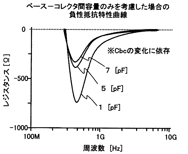
図13に、VCSOの負性抵抗特性のシミュレーション結果を示す。1[GHz]において、-220[Ω]の負性抵抗が得られている。SAW Resonatorの損失が20[Ω]以下であることを考えると、10倍の余裕度があり、十分な負性抵抗値である。
FIG. 13 shows a simulation result of the negative resistance characteristics of VCSO. Negative resistance of -220 [Ω] is obtained at 1 [GHz]. Considering that the loss of SAW Resonator is 20 [Ω] or less, there is a margin of 10 times, which is a sufficient negative resistance value.
図14に、VCSOのスプリアス特性を示す。基本波発振のため、サブハーモニクスが存在せず、ハーモニクスのみとなっていることがわかる。サブハーモニクスは発振器のJitter特性を劣化させる大きな要因であり、これが存在しないことは装置でのビットエラー等の問題を低減できる。
図15に、電源電圧に対する周波数特性を示す。同図より、周波数変動は電源電圧+3.3[V]±5[%]に対して、±2.0 [ppm]以内を実現していることがわかる。この特性は、水晶振動子を用いた一般的なVCXO等と比較しても、全く遜色のないものとなっている。また、周波数変動が電源電圧の増加に比例して負の傾きを持っている。これは、トランジスタQ1のベース・エミッタ間容量Cbeの影響が支配的であることを意味する。Cbeは、電源電圧の増加に伴い容量値が大きくなるため、発振周波数が低くなる。高周波のため、C1の値が小さく、Cbeの影響を受けやすいことが原因と考えられる。なお、電源電圧+3.3[V]において、消費電流11.5[mA]、出力レベル-1.3[dBm/50Ω]であった。
FIG. 14 shows the spurious characteristics of VCSO. It can be seen that because of the fundamental wave oscillation, there is no sub-harmonics and only harmonics. Subharmonics are a major factor that degrades the Jitter characteristics of the oscillator, and the absence of this can reduce problems such as bit errors in the device.
FIG. 15 shows frequency characteristics with respect to the power supply voltage. From the figure, it can be seen that the frequency fluctuation is within ± 2.0 [ppm] with respect to the power supply voltage +3.3 [V] ± 5 [%]. This characteristic is completely comparable to that of a general VCXO using a crystal resonator. Further, the frequency fluctuation has a negative slope in proportion to the increase of the power supply voltage. This means that the influence of the base-emitter capacitance Cbe of the transistor Q1 is dominant. Since the capacitance value of Cbe increases as the power supply voltage increases, the oscillation frequency decreases. The reason is considered to be that the value of C1 is small due to high frequency and is easily influenced by Cbe. In addition, at power supply voltage +3.3 [V], the current consumption was 11.5 [mA] and the output level was -1.3 [dBm / 50Ω].
図16に、周波数温度特性を示す。同図は、+25[℃]のときの周波数を1[GHz]に対してプラス側に50[ppm]シフトさせた場合の周波数温度特性である。同図より、周波数温度特性は-40[℃]〜+85[℃]において±60[ppm]以内の安定度を持っている。
図17に、周波数可変特性を示す。同図は、周波数温度特性と同様に周波数制御電圧における中心値+1.65[V]のときの周波数を1[GHz]からプラス側へ60[ppm]シフトさせたときの周波数可変特性である。同図より、±200[ppm]以上の広可変特性を実現できている。VCSOに要求される仕様として絶対周波数可変±100[ppm]があるが、これは周波数可変から総合安定度をさし引いたものであり、今回試作したVCSOの総合安定度±100[ppm]以内の場合、周波数可変が±200[ppm]以上あれば、仕様を満足することが可能である。しかし、周波数制御電圧値が小さいときのバラツキが大きく、今後可変幅の拡大と共にバラツキの低減についても検討をおこなっていく予定である。
FIG. 16 shows frequency temperature characteristics. The figure shows the frequency temperature characteristics when the frequency at +25 [° C.] is shifted 50 [ppm] to the plus side with respect to 1 [GHz]. From the figure, the frequency-temperature characteristics have a stability within ± 60 [ppm] from -40 [℃] to +85 [℃].
FIG. 17 shows frequency variable characteristics. This figure shows frequency variable characteristics when the frequency at the center value + 1.65 [V] in the frequency control voltage is shifted 60 [ppm] from 1 [GHz] to the plus side in the same manner as the frequency temperature characteristics. From the figure, a wide variable characteristic of ± 200 [ppm] or more is realized. There is an absolute frequency variable ± 100 [ppm] required for VCSO. This is the variable frequency minus the total stability, and within the total stability ± 100 [ppm] of the newly manufactured VCSO. In this case, the specification can be satisfied if the variable frequency is ± 200 [ppm] or more. However, the variation when the frequency control voltage value is small is large, and it is planned to study the reduction of the variation with the expansion of the variable width in the future.
図18に、位相雑音特性を示す。従来のディレイ・ライン型VCSOと比較して、Carrier近傍の位相雑音特性が非常に優れていることがわかる。従来、VCSOはPLLのように源振に起因するスプリアス成分が存在しないため、Jitter特性は良好であるが、Carrier近傍の位相雑音が悪い問題があった。しかしながら、今回提案する高周波コルピッツ発振回路ではCarrier近傍の位相雑音も良好であり、従来位相雑音が悪いため使用できなかった光伝送装置でも十分使用可能な特性を得られた。
図9の回路において負性抵抗RNは、式(1)によって求めることができ、高周波化につれて負性抵抗値の確保が困難になることを表している。ここで、IEはQ1のエミッタ電流、CbeはQ1のベース・エミッタ間容量である。
FIG. 18 shows the phase noise characteristics. Compared with the conventional delay line type VCSO, it can be seen that the phase noise characteristics in the vicinity of the carrier are very excellent. Conventionally, VCSO does not have spurious components due to source oscillation unlike PLL, so Jitter characteristics are good, but phase noise in the vicinity of the carrier is poor. However, the proposed high-frequency Colpitts oscillation circuit has good phase noise in the vicinity of the carrier, and the characteristics that can be sufficiently used even in an optical transmission apparatus that could not be used due to poor phase noise.
Negative resistance R N in the circuit of FIG. 9 may be determined by Equation (1), ensuring the negative resistance values represent be difficult as high frequency. Here, I E is the emitter current of Q 1, is C BE is the base-emitter capacitance of Q 1.
そこで、図19の如く発振回路中に共振回路(容量C2とインダクタンスL1との並列共振回路)を設けて、負性抵抗のピークを発振周波数近傍に設けられる共振回路内蔵高周波コルピッツ発振回路を提案する。
Accordingly, a high-frequency Colpitts oscillation circuit with a built-in resonance circuit in which a resonance circuit (a parallel resonance circuit of a capacitor C2 and an inductance L1) is provided in the oscillation circuit as shown in FIG. 19 and the negative resistance peak is provided near the oscillation frequency is proposed. .
図20に、高周波コルピッツ回路と比較して負性抵抗特性を示す。同図より、共振回路を内蔵して、負性抵抗のピークを発振周波数近傍に設けることにより、負性抵抗が飛躍的に増大でき、更に高周波帯域まで使用可能になると予測できる。
図20より、共振回路を内蔵することで、高周波コルピッツ回路の負性抵抗特性を大きくできることを示したが、大きすぎる負性抵抗は、異常発振、周波数安定度の落下を引き起こすため、適切に設定する必要がある。
図19の回路にて、表1のSAW Resonatorを使用した場合、発振ループ内の損失Reは式(2)で求まり、約82[Ω]である。
FIG. 20 shows negative resistance characteristics as compared with a high-frequency Colpitts circuit. From this figure, it can be predicted that by incorporating a resonance circuit and providing the peak of the negative resistance in the vicinity of the oscillation frequency, the negative resistance can be dramatically increased and further usable up to a high frequency band.
From FIG. 20, it was shown that the negative resistance characteristic of the high-frequency Colpitts circuit can be increased by incorporating a resonance circuit. However, an excessively large negative resistance causes abnormal oscillation and a drop in frequency stability. There is a need to.
In the circuit of Figure 19, when using SAW Resonator in Table 1, loss R e in the oscillation loop is Motomari formula (2) is about 82 [Omega].
Re=R1(1+C0/CL)2 (2)
従って、負性抵抗値が発振ループ内損失の約3倍である-250[Ω]となるようにエミッタ電流を小さく設計した。図21に、負性抵抗特性を示す。同図より、高周波コルピッツ発振回路が負性抵抗のピークが500[MHz]近傍にあるのに対し、共振回路内蔵高周波コルピッツ発振回路は1[GHz]近傍にピークがあることがわかる。また、発振周波数以下の領域で負性となる部分が少ないため、圧電素子の副共振や回路中の浮遊容量・配線による異常発振等の影響に強くなっている。
図22に、ドライブレベル対負性抵抗特性を示す。同図より、共振回路を高周波コルピッツ発振回路に内蔵させることで、発振開始時(小信号時)の負性抵抗は同じであるが、定常時のドライブレベルを3.2[mA]から1.8[mA]に低減できた。
R e = R 1 (1 + C 0 / C L ) 2 (2)
Therefore, the emitter current is designed to be small so that the negative resistance value is -250 [Ω], which is about three times the loss in the oscillation loop. FIG. 21 shows the negative resistance characteristics. The figure shows that the high-frequency Colpitts oscillation circuit has a negative resistance peak near 500 [MHz], whereas the resonance circuit built-in high-frequency Colpitts oscillation circuit has a peak near 1 [GHz]. In addition, since there are few negative portions in the region below the oscillation frequency, it is strongly affected by sub-resonance of the piezoelectric element and abnormal oscillation due to stray capacitance / wiring in the circuit.
FIG. 22 shows drive level versus negative resistance characteristics. From the figure, by incorporating the resonance circuit in the high-frequency Colpitts oscillation circuit, the negative resistance at the start of oscillation (at the time of small signal) is the same, but the drive level at steady state is from 3.2 [mA] to 1.8 [mA] We were able to reduce to.
以上の説明では、本発明を基本波を用いて構成するコルピッツ発振回路に適用し例示し
たが、本発明はこれに限定するのではなく3次高調波水晶振動子、5次高調波水晶振動子
を用いて構成するコルピッツ発振器にも適用することができる。また、実施例においては
電圧制御電圧源としてソース接地増幅回路やエミッタホロアを用いたものを上げたが、本
発明はこれに限定するものではない。
In the above description, the present invention is applied to the Colpitts oscillation circuit configured by using the fundamental wave, but the present invention is not limited to this. The third harmonic crystal resonator and the fifth harmonic crystal resonator are exemplified. The present invention can also be applied to a Colpitts oscillator configured using the above. In the embodiment, the common source amplifier circuit or emitter follower is used as the voltage control voltage source. However, the present invention is not limited to this.
Ra、Rb、Rc、Re、R1、R2、R3 抵抗
C1、C2、C3、C4、C5、CV、Co 容量
L1 インダクタンス
X 水晶振動子
Tr1、Tr2 トランジスタ
Vcc 電源電圧
OUT 出力端子
(A) コルピッツ発振回路
(B) 電圧制御電圧源
Ra, Rb, Rc, Re, R1, R2, R3 Resistors C1, C2, C3, C4, C5, CV, Co Capacitance L1 Inductance X Crystal resonator
Tr1, Tr2 Transistor Vcc Power supply voltage OUT Output terminal (A) Colpitts oscillation circuit (B) Voltage control voltage source
Claims (3)
3. The high frequency Colpitts oscillation circuit according to claim 2, wherein a parallel resonance circuit comprising a capacitance and an inductance is inserted and connected between the emitter of the first transistor and the ground.
Priority Applications (4)
| Application Number | Priority Date | Filing Date | Title |
|---|---|---|---|
| JP2005306588A JP2007116487A (en) | 2005-10-21 | 2005-10-21 | High frequency colpitts oscillation circuit |
| US11/468,019 US20070090889A1 (en) | 2005-10-21 | 2006-08-29 | High frequency colpitts oscillation circuit |
| EP06021879A EP1777808A1 (en) | 2005-10-21 | 2006-10-19 | High frequency Colpitts oscillation circuit |
| CNA2006101371076A CN1953319A (en) | 2005-10-21 | 2006-10-20 | High frequency colpitts oscillation circuit |
Applications Claiming Priority (1)
| Application Number | Priority Date | Filing Date | Title |
|---|---|---|---|
| JP2005306588A JP2007116487A (en) | 2005-10-21 | 2005-10-21 | High frequency colpitts oscillation circuit |
Publications (1)
| Publication Number | Publication Date |
|---|---|
| JP2007116487A true JP2007116487A (en) | 2007-05-10 |
Family
ID=37770365
Family Applications (1)
| Application Number | Title | Priority Date | Filing Date |
|---|---|---|---|
| JP2005306588A Withdrawn JP2007116487A (en) | 2005-10-21 | 2005-10-21 | High frequency colpitts oscillation circuit |
Country Status (4)
| Country | Link |
|---|---|
| US (1) | US20070090889A1 (en) |
| EP (1) | EP1777808A1 (en) |
| JP (1) | JP2007116487A (en) |
| CN (1) | CN1953319A (en) |
Cited By (3)
| Publication number | Priority date | Publication date | Assignee | Title |
|---|---|---|---|---|
| JP2010153972A (en) * | 2008-12-24 | 2010-07-08 | Nippon Dempa Kogyo Co Ltd | High-frequency colpitts circuit |
| WO2011062032A1 (en) * | 2009-11-19 | 2011-05-26 | 株式会社村田製作所 | Oscillator circuit and sensor |
| JP2015019241A (en) * | 2013-07-11 | 2015-01-29 | 新日本無線株式会社 | Oscillation circuit and method of adjusting the same |
Families Citing this family (2)
| Publication number | Priority date | Publication date | Assignee | Title |
|---|---|---|---|---|
| EP3118641B8 (en) * | 2015-07-15 | 2019-03-20 | Indian Oil Corporation Limited | An improved giant magneto-impedance (gmi) based sensing device for the detection of carburization in austenitic stainless steel |
| CN112865948A (en) * | 2021-01-20 | 2021-05-28 | 南京航空航天大学 | Three-order colpitts high-frequency chaotic signal generating circuit |
Family Cites Families (8)
| Publication number | Priority date | Publication date | Assignee | Title |
|---|---|---|---|---|
| JPS5574222A (en) * | 1978-11-30 | 1980-06-04 | Nec Corp | Temperature compensation circuit for crystal oscillator |
| JPS622813Y2 (en) * | 1979-07-20 | 1987-01-22 | ||
| US4479096A (en) * | 1981-07-20 | 1984-10-23 | Rockwell International Corporation | Voltage variable crystal controlled oscillator |
| DE19652146B4 (en) * | 1996-12-14 | 2006-06-29 | Sennheiser Electronic Gmbh & Co. Kg | Low noise oscillator circuit |
| US6606007B1 (en) * | 2001-07-31 | 2003-08-12 | Lsi Logic Corporation | Crystal oscillator with minimized Q reduction |
| JP3998233B2 (en) * | 2001-11-09 | 2007-10-24 | セイコーNpc株式会社 | Oscillation circuit and integrated circuit for oscillation |
| US7196591B2 (en) * | 2003-08-06 | 2007-03-27 | Synergy Microwave Corporation | Tunable frequency, low phase noise and low thermal drift oscillator |
| JP4259237B2 (en) * | 2003-09-05 | 2009-04-30 | エプソントヨコム株式会社 | Piezoelectric oscillator |
-
2005
- 2005-10-21 JP JP2005306588A patent/JP2007116487A/en not_active Withdrawn
-
2006
- 2006-08-29 US US11/468,019 patent/US20070090889A1/en not_active Abandoned
- 2006-10-19 EP EP06021879A patent/EP1777808A1/en not_active Withdrawn
- 2006-10-20 CN CNA2006101371076A patent/CN1953319A/en active Pending
Cited By (5)
| Publication number | Priority date | Publication date | Assignee | Title |
|---|---|---|---|---|
| JP2010153972A (en) * | 2008-12-24 | 2010-07-08 | Nippon Dempa Kogyo Co Ltd | High-frequency colpitts circuit |
| US8154355B2 (en) | 2008-12-24 | 2012-04-10 | Nihon Dempa Kogyo Co., Ltd | High-frequency colpitts circuit |
| WO2011062032A1 (en) * | 2009-11-19 | 2011-05-26 | 株式会社村田製作所 | Oscillator circuit and sensor |
| JPWO2011062032A1 (en) * | 2009-11-19 | 2013-04-04 | 株式会社村田製作所 | Oscillator circuit and sensor |
| JP2015019241A (en) * | 2013-07-11 | 2015-01-29 | 新日本無線株式会社 | Oscillation circuit and method of adjusting the same |
Also Published As
| Publication number | Publication date |
|---|---|
| EP1777808A1 (en) | 2007-04-25 |
| US20070090889A1 (en) | 2007-04-26 |
| CN1953319A (en) | 2007-04-25 |
Similar Documents
| Publication | Publication Date | Title |
|---|---|---|
| KR100756331B1 (en) | Low Phase Noise Differential LC tank VCO with Current Negative Feedback | |
| RU2404505C2 (en) | Adjustable generator with serial and parallel adjusted resonant circuits | |
| US11228280B1 (en) | Microelectromechanical system resonator-based oscillator | |
| US6380816B1 (en) | Oscillator and voltage controlled oscillator | |
| JP2007116487A (en) | High frequency colpitts oscillation circuit | |
| JP4228660B2 (en) | Voltage controlled oscillator and electronic equipment using the same | |
| JP2010041346A (en) | Quartz oscillation circuit of suboscillation suppressing type | |
| JPH10284937A (en) | Circuit for evading parasitic oscillation mode in oscillator resonance circuit | |
| JP2004297166A (en) | Temperature-compensated piezoelectric oscillator and electronic equipment using the same | |
| JP4259237B2 (en) | Piezoelectric oscillator | |
| WO2001020772A1 (en) | Oscillator mode suppression circuit | |
| JP2004040509A (en) | Oscillation circuit and electronic apparatus using the oscillation circuit | |
| JP2007103985A (en) | Crystal oscillator | |
| JP4561029B2 (en) | OSCILLATOR CIRCUIT AND ELECTRONIC DEVICE USING THE SAME | |
| US9077281B2 (en) | Oscillator circuit | |
| EP0827278A2 (en) | High stability single-port saw resonator oscillator | |
| JP2004289207A (en) | Crystal oscillator | |
| US7205856B2 (en) | Piezoelectric oscillator | |
| JP2004023568A (en) | Oscillation circuit and electronic apparatus employing the same | |
| JP2005252413A (en) | Crystal quadrature output type oscillator | |
| JP4604825B2 (en) | Piezoelectric oscillator | |
| JP2010135877A (en) | Piezoelectric oscillator | |
| JP2003060434A (en) | Oscillator and electronic apparatus using the same | |
| JP2006186860A (en) | Piezoelectric oscillator | |
| JP2004080527A (en) | Oscillator and electronic device using same |
Legal Events
| Date | Code | Title | Description |
|---|---|---|---|
| RD04 | Notification of resignation of power of attorney |
Free format text: JAPANESE INTERMEDIATE CODE: A7424 Effective date: 20070404 |
|
| A977 | Report on retrieval |
Free format text: JAPANESE INTERMEDIATE CODE: A971007 Effective date: 20081111 |
|
| A131 | Notification of reasons for refusal |
Free format text: JAPANESE INTERMEDIATE CODE: A131 Effective date: 20081118 |
|
| A761 | Written withdrawal of application |
Free format text: JAPANESE INTERMEDIATE CODE: A761 Effective date: 20090108 |