JP2012156946A - Oscillation circuit and vibration type sensor using the same - Google Patents
Oscillation circuit and vibration type sensor using the same Download PDFInfo
- Publication number
- JP2012156946A JP2012156946A JP2011016587A JP2011016587A JP2012156946A JP 2012156946 A JP2012156946 A JP 2012156946A JP 2011016587 A JP2011016587 A JP 2011016587A JP 2011016587 A JP2011016587 A JP 2011016587A JP 2012156946 A JP2012156946 A JP 2012156946A
- Authority
- JP
- Japan
- Prior art keywords
- circuit
- vibrator
- oscillation circuit
- oscillation
- conversion circuit
- Prior art date
- Legal status (The legal status is an assumption and is not a legal conclusion. Google has not performed a legal analysis and makes no representation as to the accuracy of the status listed.)
- Pending
Links
Images

Abstract
Description
本発明は、振動子の寄生抵抗や寄生容量による影響を低減して、振動式センサの測定精度を向上させ得る発振回路およびそれを用いた振動式センサに関する。 The present invention relates to an oscillation circuit that can improve the measurement accuracy of a vibration sensor by reducing the influence of parasitic resistance and capacitance of the vibrator, and a vibration sensor using the oscillation circuit.
振動式センサを用いて圧力等の物理量を測定する物理量測定装置が種々提案されている。例えば、静電駆動型振動子を用いた振動式センサの場合、振動子と電極との間に働く静電吸引力の変化に応じて振動する振動子の周波数に基づいて物理量を測定する。このような静電駆動型振動子を用いた振動式センサによる物理測定装置として、例えば特開2009−257807号公報に開示されたものがある。 Various physical quantity measuring devices that measure physical quantities such as pressure using a vibration sensor have been proposed. For example, in the case of a vibration sensor using an electrostatic drive type vibrator, the physical quantity is measured based on the frequency of the vibrator that vibrates according to a change in electrostatic attraction force acting between the vibrator and the electrode. As a physical measurement device using a vibration sensor using such an electrostatic drive type vibrator, for example, there is one disclosed in Japanese Patent Application Laid-Open No. 2009-257807.
図4に、従来の静電駆動型振動子を用いた振動式センサの基本的な構成図を示す。同図において、振動式センサ102は、固定電極1と、振動子3と、電流電圧変換回路20と、絶対値回路30と、誤差増幅器40およびオートゲインコントロール回路50を備えた駆動部と、シュミットトリガ60と、を備えた構成である。ここで、振動子3は、固定電極1に対し所定間隔で対向設置され、その形状(例えば、梁の形状)によって決定される固有振動数を持つ。
FIG. 4 shows a basic configuration diagram of a vibration type sensor using a conventional electrostatic drive type vibrator. In the figure, a
また、バイアス電圧Vbが印加される固定電極1、固定電極1と振動子3との間に働く静電吸引力、振動子3、電流電圧変換回路20、駆動部および自励振信号Viの固定電極1への帰還という一連のループによって、振動子3を固有振動数で振動させる自励振回路(正帰還ループ)が形成されている。
Further, the fixed electrode 1 to which the bias voltage Vb is applied, the electrostatic attraction force acting between the fixed electrode 1 and the vibrator 3, the vibrator 3, the current-
一般的に、圧電振動子等の振動子を用いる振動式センサの場合、振動子のQ値(共振の尖鋭度)を高めることにより非常に高い分解能、再現性、安定性が得られることが知られている。また、振動子を電気回路素子として見たとき、その共振特性は、2端子振動子、即ち、等価直列抵抗Rme、直列インダクタンスLme、直列容量Cmeの直列回路と並列容量C0との並列回路で評価できる。 In general, in the case of a vibration sensor using a vibrator such as a piezoelectric vibrator, it is known that an extremely high resolution, reproducibility, and stability can be obtained by increasing the Q value (resonance sharpness) of the vibrator. It has been. When the vibrator is viewed as an electric circuit element, the resonance characteristic is evaluated by a two-terminal vibrator, that is, a parallel circuit of a series circuit of an equivalent series resistance Rme, a series inductance Lme, and a series capacity Cme and a parallel capacity C0. it can.
しかしながら、実際には、振動子の製造プロセスにおいて、構造上、寄生抵抗や寄生容量が形成されることは避けられず、これらが振動子の共振特性(Q値やゲイン等)を悪化させてしまい、振動式センサの測定精度が低下するという事情があった。 However, in practice, in the vibrator manufacturing process, it is inevitable that parasitic resistance and parasitic capacitance are formed due to the structure, and these deteriorate the resonance characteristics (Q value, gain, etc.) of the vibrator. There was a circumstance that the measurement accuracy of the vibration sensor was lowered.
例えば、寄生抵抗について見てみると、図2(a)に示す如く、寄生抵抗Rp1およびRp2を持つ等価回路として表される。このとき、図5の電流電圧変換回路20の出力である電圧信号Voについて、Q値Q10およびゲインG10を求めると、次式で表される。
(数1)
Q10=(Lme/Cme)1/2/(Rme+Rp1+Rp2) (1)
G10=−Rf/(Rme+Rp1+Rp2) (2)
ここで、電流電圧変換回路20の帰還抵抗27の抵抗値をRfとし、また、並列容量C0≫直列容量Cmeとして並列容量C0を無視できるものとした。
For example, the parasitic resistance is represented as an equivalent circuit having parasitic resistances Rp1 and Rp2 as shown in FIG. At this time, when the Q value Q 10 and the gain G 10 are obtained for the voltage signal Vo that is the output of the current-
(Equation 1)
Q 10 = (Lme / Cme) 1/2 / (Rme + Rp1 + Rp2) (1)
G 10 = −Rf / (Rme + Rp1 + Rp2) (2)
Here, it is assumed that the resistance value of the
式(1)、(2)において、寄生抵抗が無い(Rp1=Rp2=0)理想的な場合と比較すると、寄生抵抗が形成されてRp1、Rp2が有限値を持つ場合には、Q値Q10およびゲインG10共に低下することが分かる。このようなQ値の低下は、発振の安定性を低下させ、場合によっては発振が不可能になる恐れもある。また、ゲインの低下はSN比(信号対雑音比)の悪化を招く。 In the equations (1) and (2), compared to the ideal case where there is no parasitic resistance (Rp1 = Rp2 = 0), when the parasitic resistance is formed and Rp1 and Rp2 have finite values, the Q value Q it can be seen that the decrease in both 10 and gain G 10. Such a decrease in the Q value decreases the stability of oscillation, and in some cases, oscillation may not be possible. In addition, a decrease in gain causes a deterioration in the SN ratio (signal to noise ratio).
本発明は、上記従来の事情に鑑みてなされたものであり、振動子の寄生抵抗や寄生容量による共振特性(Q値やゲイン等)への影響を低減して、安定した発振を実現し得る発振回路を提供することを目的とする。
また、本発明の他の目的は、測定精度を向上させ得る発振回路を用いた振動式センサを提供することである。
The present invention has been made in view of the above-described conventional circumstances, and can reduce the influence on the resonance characteristics (Q value, gain, etc.) due to the parasitic resistance and parasitic capacitance of the vibrator and realize stable oscillation. An object is to provide an oscillation circuit.
Another object of the present invention is to provide a vibration sensor using an oscillation circuit that can improve measurement accuracy.
上記課題を解決するために、本発明に係る発振回路は、振動子と、前記振動子の出力電流信号を電圧信号に変換する電流電圧変換回路と、を備えた発振回路であって、前記電流電圧変換回路を負性インピーダンス変換回路としたことを特徴とする。 In order to solve the above problems, an oscillation circuit according to the present invention is an oscillation circuit including a vibrator and a current-voltage conversion circuit that converts an output current signal of the vibrator into a voltage signal, and the current The voltage conversion circuit is a negative impedance conversion circuit.
また、上記発明において、前記負性インピーダンス変換回路は、演算増幅器と、 一端が前記演算増幅器の一方の入力端子に接続され、他端が前記演算増幅器の出力端子に接続され、前記一端に前記振動子の出力電流信号が入力される第1回路と、一端が前記第1回路の他端に接続され、他端が前記演算増幅器の他方の入力端子に接続される第2回路と、一端が前記第2回路の他端に接続され、他端が電源電位に接続される第3回路と、を備えたことを特徴とする。 In the above invention, the negative impedance converter circuit includes an operational amplifier, one end connected to one input terminal of the operational amplifier, the other end connected to the output terminal of the operational amplifier, and the vibration connected to the one end. A first circuit to which the output current signal of the child is input, a second circuit in which one end is connected to the other end of the first circuit, and the other end is connected to the other input terminal of the operational amplifier; And a third circuit connected to the other end of the second circuit and connected to the power supply potential at the other end.
また、上記発明において、前記第1回路、前記第2回路および前記第3回路をそれぞれ抵抗素子で構成したことを特徴とする。 In the above invention, the first circuit, the second circuit, and the third circuit are each configured by a resistance element.
また、上記発明において、前記第1回路および前記第2回路をそれぞれ抵抗素子で構成し、前記第3回路を容量性素子で構成したことを特徴とする。 In the invention described above, the first circuit and the second circuit are each configured by a resistance element, and the third circuit is configured by a capacitive element.
また、上記発明において、前記第1回路を抵抗素子および容量性素子の並列回路で構成し、前記第2回路および前記第3回路をそれぞれ抵抗素子で構成したことを特徴とする。 In the above invention, the first circuit is constituted by a parallel circuit of a resistance element and a capacitive element, and the second circuit and the third circuit are each constituted by a resistance element.
また、上記発明において、前記振動子は、静電駆動型振動子、水晶振動子、弾性表面波振動子、シリコン振動子またはセラミック振動子であることを特徴とする。 In the above invention, the vibrator is an electrostatic drive vibrator, a crystal vibrator, a surface acoustic wave vibrator, a silicon vibrator, or a ceramic vibrator.
さらに、上記発振回路を用いて、前記振動子に被測定対象の物理量が作用することを特徴とする。 Furthermore, a physical quantity to be measured acts on the vibrator using the oscillation circuit.
本発明に係る発振回路によれば、振動子の寄生抵抗や寄生容量による共振特性(Q値やゲイン等)への影響を低減または相殺することができ、発振回路の安定した発振を実現し得ると共に、振動式センサの測定精度を向上させ得る発振回路を提供することができる。また、当該発振回路を用いた振動式センサの測定精度を向上させることができる。 According to the oscillation circuit according to the present invention, the influence on the resonance characteristics (Q value, gain, etc.) due to the parasitic resistance and parasitic capacitance of the vibrator can be reduced or canceled, and stable oscillation of the oscillation circuit can be realized. In addition, an oscillation circuit that can improve the measurement accuracy of the vibration sensor can be provided. In addition, the measurement accuracy of the vibration sensor using the oscillation circuit can be improved.
以下、本発明に係る好適な実施の形態について、図面を参照しながら詳細に説明する。なお、以下の説明では、発振回路に用いる振動子を静電駆動型振動子として説明するが、これに限定されることなく、静電駆動型振動子を、他の圧電振動子、例えば水晶振動子、弾性表面波振動子、シリコン振動子またはセラミック振動子等に置き換えた場合でも同等の作用効果を奏する。 DESCRIPTION OF EMBODIMENTS Hereinafter, preferred embodiments according to the present invention will be described in detail with reference to the drawings. In the following description, the vibrator used for the oscillation circuit is described as an electrostatic drive vibrator. However, the present invention is not limited to this, and the electrostatic drive vibrator may be replaced with another piezoelectric vibrator such as a quartz crystal vibrator. Even when the element is replaced with a child, a surface acoustic wave vibrator, a silicon vibrator, a ceramic vibrator, or the like, the same effect is obtained.
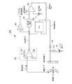
図1は本発明の一実施例に係る発振回路を用いた振動式センサの構成図である。同図において、図4(従来例)と重複する部分には同一の符号を附する。
同図において、本実施例の振動式センサ101は、固定電極1と、振動子3と、負性インピーダンス変換回路10と、絶対値回路30と、誤差増幅器40およびオートゲインコントロール回路50を備えた駆動部と、シュミットトリガ60と、を備えた構成である。なお、本実施例において、特許請求の範囲にいう振動子は静電駆動型振動子であり、図1における固定電極1および振動子3が該当する。
FIG. 1 is a configuration diagram of a vibration type sensor using an oscillation circuit according to an embodiment of the present invention. In the figure, the same reference numerals are given to the portions overlapping with FIG. 4 (conventional example).
In the figure, a
ここで、振動子3は、固定電極1に対し所定間隔で対向設置されている。また、振動子3は、その形状(例えば、梁の形状)によって決定される固有振動数を持ち、振動子3を固有振動数で振動させる自励振回路が形成されている。すなわち、バイアス電圧Vbが印加される固定電極1、固定電極1と振動子3との間に働く静電吸引力、振動子3、負性インピーダンス変換回路10、駆動部および自励振信号Viの固定電極1への帰還という一連のループによって、振動子3を固有振動数で振動させる自励振回路(正帰還ループ)が形成される。
Here, the vibrator 3 is disposed to face the fixed electrode 1 at a predetermined interval. The vibrator 3 has a natural frequency determined by its shape (for example, the shape of a beam), and a self-excited circuit that vibrates the vibrator 3 at the natural frequency is formed. That is, the fixed electrode 1 to which the bias voltage Vb is applied, the electrostatic attractive force acting between the fixed electrode 1 and the vibrator 3, the vibrator 3, the negative
振動子3の振動の動作について簡単に説明する。固定電極1と振動子3との間には、抵抗73を介してバイアス電圧Vbが印加される。固定電極1は自励振信号Viによって駆動される。なお、自励振信号Viの周波数は振動子3の固有振動数と一致する。自励振信号Viによって固定電極1に印加される電圧が変化するため、振動子3は、固定電極1と振動子3との間に働く静電吸引力の変化に応じて固有振動数で振動する。このとき、静電電流が、固定電極1と振動子3との間に形成された容量を介して固定電極1から振動子3へ流れる。そして、この静電電流が振動子3から出力されることとなる。
The vibration operation of the vibrator 3 will be briefly described. A bias voltage Vb is applied between the fixed electrode 1 and the vibrator 3 via a
この振動子3の出力である電流信号ioは、負性インピーダンス変換回路10によって電圧信号Voに変換される。すなわち、従来の構成(図5)では電流電圧変換回路20によって電流信号ioから電圧信号Voへの変換を行っていたが、本実施例の構成では負性インピーダンス変換回路10によって変換している。従来の電流電圧変換回路20を負性インピーダンス変換回路10に置き換えたことによって得られる作用効果については後述する。
The current signal io that is the output of the vibrator 3 is converted into a voltage signal Vo by the negative
変換された電圧信号Voは、シュミットトリガ60、絶対値回路30およびオートゲインコントロール回路50にそれぞれ入力される。シュミットトリガ60では、図中に付記した信号波形で示されるように、電圧信号Voを2値のディジタル信号に波形整形した周波数信号を生成する。なお、この周波数信号は物理量測定装置の演算処理部(図示せず)に供給され、測定対象の圧力等の物理量が求められることとなる。
The converted voltage signal Vo is input to the
また、絶対値回路30では、電圧信号Voの振幅に一致する直流電圧を生成し、これを絶対値信号Vabsとして誤差増幅器40に出力する。誤差増幅器40では、絶対値信号Vabsの設定電圧Vrefに対する誤差(差分)を増幅して、これを誤差信号Verrとしてオートゲインコントロール回路50に出力する。オートゲインコントロール回路50では、電圧信号Voおよび誤差信号Verrに基づき、電圧信号Voの振幅を設定電圧Vrefに一致させた自励振信号Viを生成して固定電極1へ出力する。
The
なお、本実施例の振動式センサ101では、測定対象の圧力等の物理量が振動子3に作用することによって、振動子13の歪が変化し、固有振動数が変化する。すなわち、振動子3に印加される圧力等の物理量に応じて、振動子3の固有振動数は変化する。電圧信号Voの周波数は振動子3の固有振動数と一致するため、電圧信号Voの周波数によって圧力等の物理量を知ることができる。
In the
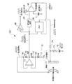
次に、図2を参照して、本実施例の振動式センサで用いる発振回路について説明する。ここで、図2は実施例の振動式センサで用いる発振回路の説明図であり、図2(a)は静電駆動型振動子(図1中の固定電極1および振動子3)の等価回路、図2(b)は負性インピーダンス変換回路10の回路図である。
Next, an oscillation circuit used in the vibration type sensor of this embodiment will be described with reference to FIG. Here, FIG. 2 is an explanatory diagram of an oscillation circuit used in the vibration type sensor of the embodiment, and FIG. 2A is an equivalent circuit of an electrostatic drive type vibrator (fixed electrode 1 and vibrator 3 in FIG. 1). FIG. 2B is a circuit diagram of the negative
上述したように、静電駆動型振動子を電気回路素子として見たとき、その共振特性を評価するための等価回路は、等価直列抵抗Rme、直列インダクタンスLme、直列容量Cmeの直列回路と並列容量C0との並列回路で表される。また、本実施例では、静電駆動型振動子の製造プロセスにおいて寄生抵抗が形成されたケースを想定する。この場合、等価回路は、図2(a)に示すように、該並列回路に対してそれぞれ直列に寄生抵抗Rp1およびRp2が接続されたものとなる。 As described above, when an electrostatically driven vibrator is viewed as an electric circuit element, an equivalent circuit for evaluating the resonance characteristics includes a series circuit of an equivalent series resistance Rme, a series inductance Lme, and a series capacitance Cme, and a parallel capacitance. It is represented by a parallel circuit with C0. In this embodiment, a case is assumed in which parasitic resistance is formed in the manufacturing process of the electrostatic drive type vibrator. In this case, as shown in FIG. 2A, the equivalent circuit has parasitic resistances Rp1 and Rp2 connected in series to the parallel circuit.
また、本実施例では、負性インピーダンス変換回路10を、演算増幅器14並びに抵抗11,12および13で構成する。すなわち、負性インピーダンス変換回路10は、演算増幅器14と、一端が演算増幅器14の一方の入力端子(−)に接続され、他端が演算増幅器14の出力端子(ノードN2)に接続され、一端(ノードN1)に静電駆動型振動子の出力である電流信号ioが入力される第1抵抗11と、一端が第1抵抗11の他端(ノードN2)に接続され、他端が演算増幅器14の他方の入力端子(+)に接続される第2抵抗12と、一端が第2抵抗12の他端(ノードN3)に接続され、他端が電源電位Vgに接続される第3抵抗13と、を備えた構成である。
In the present embodiment, the negative
ここで、第1抵抗11,第2抵抗12および第3抵抗13の抵抗値をそれぞれR1,R2およびR3とし、演算増幅器14を理想のものとすれば、負性インピーダンス変換回路10の入力インピーダンスZiは次式となる。
(数2)
Zi=−R1・R3/R2 (3)
すなわち、入力側から負性インピーダンス変換回路10を見たとき、負性インピーダンス(負性抵抗)が観測されることになる。
Here, if the resistance values of the
(Equation 2)
Zi = -R1 / R3 / R2 (3)
That is, when the negative
また、このとき、負性インピーダンス変換回路10の出力である電圧信号Voについて、Q値Q1およびゲインG1を求めると、次式で表される。
(数3)
Q1=(Lme/Cme)1/2/(Rme+Rp1+Rp2+Zi) (4)
G1=Zi・(1+R3/R2)/(Rme+Rp1+Rp2+Zi) (5)
ここで、従来と同様、並列容量C0≫直列容量Cmeとして並列容量C0を無視できるものとした。
At this time, when the Q value Q 1 and the gain G 1 are obtained for the voltage signal Vo that is the output of the negative
(Equation 3)
Q 1 = (Lme / Cme) 1/2 / (Rme + Rp1 + Rp2 + Zi) (4)
G 1 = Zi · (1 + R3 / R2) / (Rme + Rp1 + Rp2 + Zi) (5)
Here, as in the conventional case, it is assumed that the parallel capacitance C0 can be ignored as the parallel capacitance C0 >> the series capacitance Cme.
まず、Q値について従来の式(1)と本実施例の式(4)とを比較すると、式(4)の分母で加算される入力インピーダンスZiは負値であり、寄生抵抗の形成による増分Rp1およびRp2を負性インピーダンス変換回路10の入力インピーダンスZiによって相殺できることが分かる。
First, comparing the conventional formula (1) with the formula (4) of the present embodiment with respect to the Q value, the input impedance Zi added in the denominator of the formula (4) is a negative value, and the increment due to the formation of the parasitic resistance It can be seen that Rp1 and Rp2 can be canceled by the input impedance Zi of the negative
このように、本実施例の発振回路によれば、寄生抵抗の形成によるQ値の低下を抑制して(従来よりもQ値を上昇させて)安定した発振を実現することができると共に、高い分解能を実現することができる。また、その結果として、当該発振回路を用いた振動式センサの測定精度を向上させることができる。 As described above, according to the oscillation circuit of the present embodiment, it is possible to suppress the decrease in the Q value due to the formation of the parasitic resistance (by increasing the Q value as compared with the prior art) and realize stable oscillation. Resolution can be realized. As a result, the measurement accuracy of the vibration sensor using the oscillation circuit can be improved.
また、ゲインについて従来の式(2)と本実施例の式(5)とを比較すると、式(5)の分母で加算される入力インピーダンスZiは負値であり、寄生抵抗の形成による増分Rp1およびRp2を負性インピーダンス変換回路10の入力インピーダンスZiによって相殺できることが分かる。また同時に、第2抵抗12と第3抵抗13の抵抗値比(R3/R2)をより大きな値とすることにより、ゲインを上昇させることができることも分かる。
Further, when the conventional equation (2) and the equation (5) of the present embodiment are compared with respect to the gain, the input impedance Zi added in the denominator of the equation (5) is a negative value, and the increment Rp1 due to the formation of the parasitic resistance. And Rp2 can be canceled by the input impedance Zi of the negative
このように、本実施例の発振回路によれば、寄生抵抗の形成によるゲインの低下を抑制して(従来よりもゲインを上昇させて)SN比を改善することができる。また、その結果として、当該発振回路を用いた振動式センサのSN比をも改善させることができる。
(変形例)
As described above, according to the oscillation circuit of the present embodiment, it is possible to improve the SN ratio by suppressing a decrease in gain due to the formation of parasitic resistance (by increasing the gain as compared with the prior art). As a result, the SN ratio of the vibration sensor using the oscillation circuit can also be improved.
(Modification)
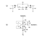
次に、変形例について図3を参照して説明する。本変形例では、静電駆動型振動子の製造プロセスにおいて寄生抵抗および寄生容量が形成され、発振回路の共振特性(Q値やゲイン等)への影響があることを想定している。ここで、図3は変形例の振動式センサで用いる発振回路の説明図であり、図3(a)は静電駆動型振動子(固定電極1および振動子3)の等価回路、図3(b)は負性インピーダンス変換回路の回路図である。なお、振動式センサの構成は実施例の構成(図1)において、図2(b)で示した負性インピーダンス変換回路の回路構成を図3(b)で置き換えたものとなる。 Next, a modification will be described with reference to FIG. In this modified example, it is assumed that parasitic resistance and parasitic capacitance are formed in the manufacturing process of the electrostatic drive type vibrator, and the resonance characteristics (Q value, gain, etc.) of the oscillation circuit are affected. Here, FIG. 3 is an explanatory diagram of an oscillation circuit used in the vibration type sensor of the modification, FIG. 3A is an equivalent circuit of the electrostatic drive type vibrator (fixed electrode 1 and vibrator 3), and FIG. b) is a circuit diagram of a negative impedance conversion circuit. The configuration of the vibration type sensor is the same as the configuration of the embodiment (FIG. 1) except that the circuit configuration of the negative impedance conversion circuit shown in FIG. 2 (b) is replaced with FIG. 3 (b).
静電駆動型振動子の製造プロセスで寄生抵抗および寄生容量が形成される場合には、等価回路は、図3(a)に示すように、等価直列抵抗Rme、直列インダクタンスLme、直列容量Cmeの直列回路と並列容量C0との並列回路に対して、直列に寄生抵抗Rp1およびRp2が、また並列に寄生容量Cp1およびCp2がそれぞれ接続されたものとなる。 When parasitic resistance and parasitic capacitance are formed in the manufacturing process of the electrostatic drive type vibrator, the equivalent circuit includes an equivalent series resistance Rme, a series inductance Lme, and a series capacitance Cme as shown in FIG. For the parallel circuit of the series circuit and the parallel capacitor C0, the parasitic resistors Rp1 and Rp2 are connected in series, and the parasitic capacitors Cp1 and Cp2 are connected in parallel, respectively.
本変形例では、負性インピーダンス変換回路を、演算増幅器25、抵抗21〜23並びにキャパシタ24で構成する。すなわち、負性インピーダンス変換回路は、演算増幅器25と、一端が演算増幅器25の一方の入力端子(−)に接続され、他端が演算増幅器25の出力端子(ノードN2)に接続され、一端(ノードN1)に静電駆動型振動子の出力である電流信号ioが入力される第1抵抗21およびキャパシタ24の並列回路と、一端が並列回路の他端(ノードN2)に接続され、他端が演算増幅器25の他方の入力端子(+)に接続される第2抵抗22と、一端が第2抵抗22の他端(ノードN3)に接続され、他端が電源電位Vgに接続される第3抵抗23と、を備えた構成である。ここで、第1抵抗21、第2抵抗22および第3抵抗23の抵抗値をそれぞれR1,R2およびR2とし、キャパシタ24の容量値をC4とする。
In this modification, the negative impedance conversion circuit includes an
ここでは、式に基づく説明を省略するが、実施例と同様に考えることができる。つまり、入力側から負性インピーダンス変換回路を見たとき、負性インピーダンスが観測されることとなる。また、Q値およびゲインについて、寄生抵抗の形成による増分Rp1およびRp2、並びに、寄生容量の形成による増分Cp1およびCp2を負性インピーダンス変換回路の入力インピーダンスZiによって相殺または低減することができる。 Here, explanation based on the formula is omitted, but it can be considered in the same manner as in the embodiment. That is, when the negative impedance conversion circuit is viewed from the input side, the negative impedance is observed. Further, regarding the Q value and the gain, the increments Rp1 and Rp2 due to the formation of the parasitic resistance and the increments Cp1 and Cp2 due to the formation of the parasitic capacitance can be canceled or reduced by the input impedance Zi of the negative impedance conversion circuit.
したがって、本変形例の発振回路によれば、寄生抵抗および寄生容量の形成によるQ値の低下を抑制して(従来よりもQ値を上昇させて)安定した発振を実現することができると共に、高い分解能を実現することができる。また、その結果として、当該発振回路を用いた振動式センサの測定精度を向上させることができる。また、寄生抵抗および寄生容量の形成によるゲインの低下を抑制して(従来よりもゲインを上昇させて)SN比を改善することができ、その結果として、当該発振回路を用いた振動式センサのSN比をも改善させることができる。 Therefore, according to the oscillation circuit of the present modification, it is possible to realize stable oscillation by suppressing a decrease in the Q value due to the formation of parasitic resistance and parasitic capacitance (increasing the Q value as compared with the prior art) High resolution can be achieved. As a result, the measurement accuracy of the vibration sensor using the oscillation circuit can be improved. In addition, it is possible to improve the SN ratio by suppressing a decrease in gain due to the formation of parasitic resistance and parasitic capacitance (by increasing the gain as compared with the prior art). As a result, the vibration sensor using the oscillation circuit can be improved. The S / N ratio can also be improved.
なお、発振回路の共振特性(Q値やゲイン等)に対して、静電駆動型振動子の製造プロセスにおける寄生容量による影響が寄生抵抗による影響に比べて相対的に大きい場合についても、本変形例の発振回路を適用することにより、同等の効果を奏することができる。すなわち、寄生容量の形成によるQ値の低下を抑制して安定した発振を実現することができると共に、高い分解能を実現し、また、その結果として、当該発振回路を用いた振動式センサの測定精度を向上させることができる。また、寄生容量の形成によるゲインの低下を抑制してSN比を改善することができ、その結果として、当該発振回路を用いた振動式センサのSN比をも改善させることができる。
(その他の変形)
This modification is also applied to the case where the influence of parasitic capacitance in the manufacturing process of the electrostatic drive vibrator is relatively larger than the influence of parasitic resistance on the resonance characteristics (Q value, gain, etc.) of the oscillation circuit. By applying the example oscillation circuit, an equivalent effect can be obtained. That is, stable oscillation can be realized by suppressing a decrease in Q value due to the formation of parasitic capacitance, and high resolution can be realized. As a result, measurement accuracy of a vibration sensor using the oscillation circuit can be realized. Can be improved. In addition, it is possible to improve the SN ratio by suppressing a decrease in gain due to the formation of parasitic capacitance. As a result, the SN ratio of the vibration sensor using the oscillation circuit can also be improved.
(Other variations)
以上、本発明の好ましい実施例および変形例について詳述したが、本発明に係る発振回路およびそれを用いた振動式センサは、上述した実施例および変形例に限定されるものではなく、特許請求の範囲に記載された本発明の要旨の範囲内において、種々の変形、変更が可能である。 The preferred embodiments and modifications of the present invention have been described above in detail. However, the oscillation circuit and the vibration sensor using the same according to the present invention are not limited to the above-described embodiments and modifications, and are claimed. Various modifications and changes can be made within the scope of the gist of the present invention described in the above.
例えば、上述したように、静電駆動型振動子を他の圧電振動子に置き換えても良い。他の圧電振動子としては、例えば、水晶振動子、弾性表面波振動子(若しくはSAW(Surface Acoustic Wave)振動子)、シリコン振動子、セラミック振動子、端面反射振動子、またはバルク振動子等がある。これらに置き換えた場合でも実施例および変形例と同等の効果を奏することができる。 For example, as described above, the electrostatic drive type vibrator may be replaced with another piezoelectric vibrator. Examples of other piezoelectric vibrators include a quartz crystal vibrator, a surface acoustic wave vibrator (or a SAW (Surface Acoustic Wave) vibrator), a silicon vibrator, a ceramic vibrator, an end surface reflecting vibrator, or a bulk vibrator. is there. Even when these are replaced, the same effects as those of the embodiment and the modification can be obtained.
また、振動子は圧電振動子に限定されることなく、他の振動子であっても良い。振動子の製造プロセスで、構造上、寄生抵抗や寄生容量が形成されるものについて、実施例および変形例と同様に負性インピーダンス変換回路を付加することにより、寄生抵抗や寄生容量の形成によるQ値およびゲインの低下を抑制することが可能である。 Further, the vibrator is not limited to the piezoelectric vibrator but may be another vibrator. In the manufacturing process of the vibrator, in which parasitic resistance and parasitic capacitance are formed due to the structure, a negative impedance conversion circuit is added in the same manner as in the embodiment and the modified example, so that the Q due to the formation of parasitic resistance and parasitic capacitance is obtained. It is possible to suppress a decrease in value and gain.
また、負性インピーダンス変換回路の構成は、例示した回路構成に限定されることなく他の回路構成であっても良い。演算増幅器を用いた構成のものではなく、例えば特許第3907633号に開示されているような差動型負性インピーダンス変換回路を用いることも可能である。 Further, the configuration of the negative impedance conversion circuit is not limited to the illustrated circuit configuration, and may be another circuit configuration. For example, a differential negative impedance conversion circuit as disclosed in Japanese Patent No. 3907633 can be used instead of an operational amplifier.
さらに、振動子による発振回路に限定されることなく、LC発振回路などの他の発振回路に負性インピーダンス変換回路を付加する構成も考えられる。発振回路を構成する各素子の製造プロセスで、構造上、寄生抵抗や寄生容量が形成されるものについて、実施例および変形例と同様に負性インピーダンス変換回路を付加することにより、寄生抵抗や寄生容量の形成によるQ値およびゲインの低下を抑制することが可能である。 Furthermore, the present invention is not limited to an oscillation circuit using a vibrator, and a configuration in which a negative impedance conversion circuit is added to another oscillation circuit such as an LC oscillation circuit is also conceivable. In the manufacturing process of each element constituting the oscillation circuit, a parasitic resistance or parasitic capacitance is structurally formed. By adding a negative impedance conversion circuit in the same manner as in the embodiment and the modification, parasitic resistance and parasitic capacitance are added. It is possible to suppress a decrease in Q value and gain due to the formation of a capacitor.
1 固定電極
3 振動子
10 負性インピーダンス変換回路
14,18,25 演算増幅器
11〜13,15,16,21〜23,73 抵抗
17,24,74 キャパシタ
30 絶対値回路
40 誤差増幅器
50 オートゲインコントロール回路
60 シュミットトリガ
71,72 電源
101 振動式センサ
io 電流信号
Vo 電圧信号
Vb バイアス電圧
Vref 設定電圧
Verr 誤差信号
Vi 自励振信号
Vg 電源電位
DESCRIPTION OF SYMBOLS 1 Fixed electrode 3
Claims (7)
前記電流電圧変換回路を負性インピーダンス変換回路としたことを特徴とする発振回路。 An oscillation circuit comprising a vibrator and a current-voltage conversion circuit that converts an output current signal of the vibrator into a voltage signal,
An oscillation circuit characterized in that the current-voltage conversion circuit is a negative impedance conversion circuit.
演算増幅器と、
一端が前記演算増幅器の一方の入力端子に接続され、他端が前記演算増幅器の出力端子に接続され、前記一端に前記振動子の出力電流信号が入力される第1回路と、
一端が前記第1回路の他端に接続され、他端が前記演算増幅器の他方の入力端子に接続される第2回路と、
一端が前記第2回路の他端に接続され、他端が電源電位に接続される第3回路と、
を備えたことを特徴とする発振回路。 The negative impedance converter circuit is
An operational amplifier;
A first circuit in which one end is connected to one input terminal of the operational amplifier, the other end is connected to an output terminal of the operational amplifier, and an output current signal of the vibrator is input to the one end;
A second circuit having one end connected to the other end of the first circuit and the other end connected to the other input terminal of the operational amplifier;
A third circuit having one end connected to the other end of the second circuit and the other end connected to a power supply potential;
An oscillation circuit comprising:
A vibration type sensor using the oscillation circuit according to claim 1, wherein a physical quantity to be measured acts on the vibrator.
Priority Applications (1)
| Application Number | Priority Date | Filing Date | Title |
|---|---|---|---|
| JP2011016587A JP2012156946A (en) | 2011-01-28 | 2011-01-28 | Oscillation circuit and vibration type sensor using the same |
Applications Claiming Priority (1)
| Application Number | Priority Date | Filing Date | Title |
|---|---|---|---|
| JP2011016587A JP2012156946A (en) | 2011-01-28 | 2011-01-28 | Oscillation circuit and vibration type sensor using the same |
Publications (1)
| Publication Number | Publication Date |
|---|---|
| JP2012156946A true JP2012156946A (en) | 2012-08-16 |
Family
ID=46838175
Family Applications (1)
| Application Number | Title | Priority Date | Filing Date |
|---|---|---|---|
| JP2011016587A Pending JP2012156946A (en) | 2011-01-28 | 2011-01-28 | Oscillation circuit and vibration type sensor using the same |
Country Status (1)
| Country | Link |
|---|---|
| JP (1) | JP2012156946A (en) |
Cited By (5)
| Publication number | Priority date | Publication date | Assignee | Title |
|---|---|---|---|---|
| JP2015090352A (en) * | 2013-11-07 | 2015-05-11 | セイコーエプソン株式会社 | Detector, sensor, electronic apparatus and movable body |
| CN105094198A (en) * | 2014-05-23 | 2015-11-25 | 横河电机株式会社 | Current-to-voltage conversion circuit and self-oscillation circuit |
| JP2017158419A (en) * | 2016-03-01 | 2017-09-07 | ヤマハ株式会社 | Damping device |
| JP2020030165A (en) * | 2018-08-24 | 2020-02-27 | 日本電信電話株式会社 | Common-mode voltage measuring apparatus and common-mode voltage measuring method |
| JP2021016126A (en) * | 2019-07-16 | 2021-02-12 | Necプラットフォームズ株式会社 | Oscillation circuit |
Citations (6)
| Publication number | Priority date | Publication date | Assignee | Title |
|---|---|---|---|---|
| JPS59161713U (en) * | 1983-04-14 | 1984-10-30 | ソニー株式会社 | VCO |
| JPH03254507A (en) * | 1989-11-23 | 1991-11-13 | Catena Micro Electron Bv | Voltage control oscillator |
| JPH08204451A (en) * | 1995-01-20 | 1996-08-09 | Toyo Commun Equip Co Ltd | Oscillator and filter |
| JP2002174520A (en) * | 2000-12-08 | 2002-06-21 | Kinseki Ltd | Oscillating circuit and angular velocity sensor using the same |
| JP2002368541A (en) * | 2001-04-27 | 2002-12-20 | Tektronix Inc | Oscillator |
| JP2010268427A (en) * | 2009-02-27 | 2010-11-25 | Commissariat A L'energie Atomique Et Aux Energies Alternatives | Transistor-based micrometric or nanometric resonant device |
-
2011
- 2011-01-28 JP JP2011016587A patent/JP2012156946A/en active Pending
Patent Citations (6)
| Publication number | Priority date | Publication date | Assignee | Title |
|---|---|---|---|---|
| JPS59161713U (en) * | 1983-04-14 | 1984-10-30 | ソニー株式会社 | VCO |
| JPH03254507A (en) * | 1989-11-23 | 1991-11-13 | Catena Micro Electron Bv | Voltage control oscillator |
| JPH08204451A (en) * | 1995-01-20 | 1996-08-09 | Toyo Commun Equip Co Ltd | Oscillator and filter |
| JP2002174520A (en) * | 2000-12-08 | 2002-06-21 | Kinseki Ltd | Oscillating circuit and angular velocity sensor using the same |
| JP2002368541A (en) * | 2001-04-27 | 2002-12-20 | Tektronix Inc | Oscillator |
| JP2010268427A (en) * | 2009-02-27 | 2010-11-25 | Commissariat A L'energie Atomique Et Aux Energies Alternatives | Transistor-based micrometric or nanometric resonant device |
Cited By (15)
| Publication number | Priority date | Publication date | Assignee | Title |
|---|---|---|---|---|
| JP2015090352A (en) * | 2013-11-07 | 2015-05-11 | セイコーエプソン株式会社 | Detector, sensor, electronic apparatus and movable body |
| US10063217B2 (en) | 2014-05-23 | 2018-08-28 | Yokogawa Electric Corporation | Current-to-voltage conversion circuit and self-oscillation circuit |
| EP2960624A3 (en) * | 2014-05-23 | 2016-06-22 | Yokogawa Electric Corporation | Current-to-voltage conversion circuit and self-oscillation circuit |
| CN105094198A (en) * | 2014-05-23 | 2015-11-25 | 横河电机株式会社 | Current-to-voltage conversion circuit and self-oscillation circuit |
| JP2015222905A (en) * | 2014-05-23 | 2015-12-10 | 横河電機株式会社 | Current/voltage conversion circuit and self-excited oscillation circuit |
| CN108700901B (en) * | 2016-03-01 | 2020-11-20 | 雅马哈株式会社 | Vibration control device |
| JP2017158419A (en) * | 2016-03-01 | 2017-09-07 | ヤマハ株式会社 | Damping device |
| WO2017150267A1 (en) * | 2016-03-01 | 2017-09-08 | ヤマハ株式会社 | Vibration control device |
| CN108700901A (en) * | 2016-03-01 | 2018-10-23 | 雅马哈株式会社 | Vibration control apparatus |
| US11211545B2 (en) | 2016-03-01 | 2021-12-28 | Yamaha Corporation | Vibration controller |
| JP2020030165A (en) * | 2018-08-24 | 2020-02-27 | 日本電信電話株式会社 | Common-mode voltage measuring apparatus and common-mode voltage measuring method |
| WO2020040310A1 (en) * | 2018-08-24 | 2020-02-27 | 日本電信電話株式会社 | Common mode voltage measuring device and common mode voltage measuring method |
| JP7172282B2 (en) | 2018-08-24 | 2022-11-16 | 日本電信電話株式会社 | COMMON MODE VOLTAGE MEASUREMENT DEVICE AND COMMON MODE VOLTAGE MEASUREMENT METHOD |
| US11525845B2 (en) | 2018-08-24 | 2022-12-13 | Nippon Telegraph And Telephone Corporation | Common mode voltage measuring device and common mode voltage measuring method |
| JP2021016126A (en) * | 2019-07-16 | 2021-02-12 | Necプラットフォームズ株式会社 | Oscillation circuit |
Similar Documents
| Publication | Publication Date | Title |
|---|---|---|
| JP4671305B2 (en) | Physical quantity sensor | |
| US9000833B2 (en) | Compensation of changes in MEMS capacitive transduction | |
| JP2015525872A5 (en) | ||
| JP2012156946A (en) | Oscillation circuit and vibration type sensor using the same | |
| KR20040086789A (en) | Vibration type angular velocity sensor | |
| US11421992B2 (en) | Physical quantity detection circuit and physical quantity detection device | |
| US7343802B2 (en) | Dynamic-quantity sensor | |
| US9459100B2 (en) | Stepped sinusoidal drive for vibratory gyroscopes | |
| JP5060749B2 (en) | Sensing device | |
| US9252707B2 (en) | MEMS mass bias to track changes in bias conditions and reduce effects of flicker noise | |
| WO2013132842A1 (en) | Load sensor | |
| US11467176B2 (en) | Physical quantity detection circuit and physical quantity detection device | |
| JP5745834B2 (en) | Compensated micro / nano resonator with improved capacitance detection and manufacturing method thereof | |
| RU2725261C1 (en) | Linear acceleration sensor | |
| JP2008157766A (en) | Acceleration detecting device | |
| JP4449383B2 (en) | Oscillator circuit | |
| JP2013019834A (en) | Angular velocity detection circuit, integrated circuit device and angular velocity detection device | |
| JP6220618B2 (en) | Resonant circuit and oscillation circuit | |
| US11855653B2 (en) | Physical quantity detection circuit, physical quantity sensor, and method of operation of physical quantity detection circuit | |
| JP3849014B2 (en) | High frequency oscillation circuit | |
| JP6212343B2 (en) | Resonant circuit and oscillation circuit | |
| JP2008157767A (en) | Acceleration detecting device | |
| JPH08205279A (en) | Damping inductance reduction circuit for electromagnetic conversion oscillator | |
| JP6148894B2 (en) | Oscillator circuit | |
| JP2004061282A (en) | Surface potential measuring device |
Legal Events
| Date | Code | Title | Description |
|---|---|---|---|
| A621 | Written request for application examination |
Free format text: JAPANESE INTERMEDIATE CODE: A621 Effective date: 20131107 |
|
| A977 | Report on retrieval |
Free format text: JAPANESE INTERMEDIATE CODE: A971007 Effective date: 20140415 |
|
| A131 | Notification of reasons for refusal |
Free format text: JAPANESE INTERMEDIATE CODE: A131 Effective date: 20140513 |
|
| A521 | Request for written amendment filed |
Free format text: JAPANESE INTERMEDIATE CODE: A523 Effective date: 20140612 |
|
| A131 | Notification of reasons for refusal |
Free format text: JAPANESE INTERMEDIATE CODE: A131 Effective date: 20141028 |
|
| A521 | Request for written amendment filed |
Free format text: JAPANESE INTERMEDIATE CODE: A523 Effective date: 20141217 |
|
| A02 | Decision of refusal |
Free format text: JAPANESE INTERMEDIATE CODE: A02 Effective date: 20150330 |