JP4028131B2 - Photoresist polymer and method for producing the same, photoresist composition, and method for forming photoresist pattern - Google Patents
Photoresist polymer and method for producing the same, photoresist composition, and method for forming photoresist pattern Download PDFInfo
- Publication number
- JP4028131B2 JP4028131B2 JP12538199A JP12538199A JP4028131B2 JP 4028131 B2 JP4028131 B2 JP 4028131B2 JP 12538199 A JP12538199 A JP 12538199A JP 12538199 A JP12538199 A JP 12538199A JP 4028131 B2 JP4028131 B2 JP 4028131B2
- Authority
- JP
- Japan
- Prior art keywords
- photoresist
- carboxylate
- polymer
- butyl
- norbornene
- Prior art date
- Legal status (The legal status is an assumption and is not a legal conclusion. Google has not performed a legal analysis and makes no representation as to the accuracy of the status listed.)
- Expired - Fee Related
Links
- 229920002120 photoresistant polymer Polymers 0.000 title claims description 102
- 238000000034 method Methods 0.000 title claims description 54
- 238000004519 manufacturing process Methods 0.000 title claims description 23
- 239000000203 mixture Substances 0.000 title claims description 20
- 229920000642 polymer Polymers 0.000 claims description 52
- WYURNTSHIVDZCO-UHFFFAOYSA-N Tetrahydrofuran Chemical group C1CCOC1 WYURNTSHIVDZCO-UHFFFAOYSA-N 0.000 claims description 44
- OZAIFHULBGXAKX-UHFFFAOYSA-N 2,2'-azo-bis-isobutyronitrile Substances N#CC(C)(C)N=NC(C)(C)C#N OZAIFHULBGXAKX-UHFFFAOYSA-N 0.000 claims description 33
- HDFGOPSGAURCEO-UHFFFAOYSA-N N-ethylmaleimide Chemical compound CCN1C(=O)C=CC1=O HDFGOPSGAURCEO-UHFFFAOYSA-N 0.000 claims description 28
- BZBMBZJUNPMEBD-UHFFFAOYSA-N tert-butyl bicyclo[2.2.1]hept-2-ene-5-carboxylate Chemical compound C1C2C(C(=O)OC(C)(C)C)CC1C=C2 BZBMBZJUNPMEBD-UHFFFAOYSA-N 0.000 claims description 27
- PFDKMHNKWZYRPM-UHFFFAOYSA-N tert-butyl bicyclo[2.2.2]oct-2-ene-5-carboxylate Chemical compound C1CC2C(C(=O)OC(C)(C)C)CC1C=C2 PFDKMHNKWZYRPM-UHFFFAOYSA-N 0.000 claims description 26
- -1 diphenyliodo Chemical class 0.000 claims description 23
- YLQBMQCUIZJEEH-UHFFFAOYSA-N tetrahydrofuran Natural products C=1C=COC=1 YLQBMQCUIZJEEH-UHFFFAOYSA-N 0.000 claims description 22
- MDXKEHHAIMNCSW-UHFFFAOYSA-N 3-propylpyrrole-2,5-dione Chemical compound CCCC1=CC(=O)NC1=O MDXKEHHAIMNCSW-UHFFFAOYSA-N 0.000 claims description 21
- MYBZOQDIRORKOI-UHFFFAOYSA-N 3-hydroxypropyl bicyclo[2.2.1]hept-2-ene-5-carboxylate Chemical compound C1C2C(C(=O)OCCCO)CC1C=C2 MYBZOQDIRORKOI-UHFFFAOYSA-N 0.000 claims description 15
- 238000006116 polymerization reaction Methods 0.000 claims description 14
- 150000001875 compounds Chemical class 0.000 claims description 13
- PHSXOZKMZYKHLY-UHFFFAOYSA-N 2-hydroxyethyl bicyclo[2.2.1]hept-2-ene-5-carboxylate Chemical compound C1C2C(C(=O)OCCO)CC1C=C2 PHSXOZKMZYKHLY-UHFFFAOYSA-N 0.000 claims description 12
- FIAUVBFWUHSYMM-UHFFFAOYSA-N 3-hydroxypropyl bicyclo[2.2.2]oct-2-ene-5-carboxylate Chemical compound C1CC2C(C(=O)OCCCO)CC1C=C2 FIAUVBFWUHSYMM-UHFFFAOYSA-N 0.000 claims description 11
- 239000012299 nitrogen atmosphere Substances 0.000 claims description 10
- 239000003960 organic solvent Substances 0.000 claims description 10
- 239000002244 precipitate Substances 0.000 claims description 10
- ITMCEJHCFYSIIV-UHFFFAOYSA-M triflate Chemical compound [O-]S(=O)(=O)C(F)(F)F ITMCEJHCFYSIIV-UHFFFAOYSA-M 0.000 claims description 10
- ZWEHNKRNPOVVGH-UHFFFAOYSA-N 2-Butanone Chemical compound CCC(C)=O ZWEHNKRNPOVVGH-UHFFFAOYSA-N 0.000 claims description 9
- UHOVQNZJYSORNB-UHFFFAOYSA-N Benzene Chemical compound C1=CC=CC=C1 UHOVQNZJYSORNB-UHFFFAOYSA-N 0.000 claims description 9
- ZMXDDKWLCZADIW-UHFFFAOYSA-N N,N-Dimethylformamide Chemical compound CN(C)C=O ZMXDDKWLCZADIW-UHFFFAOYSA-N 0.000 claims description 9
- YXFVVABEGXRONW-UHFFFAOYSA-N Toluene Chemical compound CC1=CC=CC=C1 YXFVVABEGXRONW-UHFFFAOYSA-N 0.000 claims description 9
- 239000003795 chemical substances by application Substances 0.000 claims description 9
- 230000007261 regionalization Effects 0.000 claims description 9
- 150000003839 salts Chemical class 0.000 claims description 9
- GJFDBYRHAZJJBP-UHFFFAOYSA-N 3-tert-butylpyrrole-2,5-dione Chemical compound CC(C)(C)C1=CC(=O)NC1=O GJFDBYRHAZJJBP-UHFFFAOYSA-N 0.000 claims description 8
- 235000010290 biphenyl Nutrition 0.000 claims description 8
- 239000004305 biphenyl Substances 0.000 claims description 8
- 125000006267 biphenyl group Chemical group 0.000 claims description 8
- ZUOUZKKEUPVFJK-UHFFFAOYSA-N phenylbenzene Natural products C1=CC=CC=C1C1=CC=CC=C1 ZUOUZKKEUPVFJK-UHFFFAOYSA-N 0.000 claims description 8
- AQTMPYCVJDXCIR-UHFFFAOYSA-N 2-hydroxyethyl bicyclo[2.2.2]oct-2-ene-5-carboxylate Chemical compound C1CC2C(C(=O)OCCO)CC1C=C2 AQTMPYCVJDXCIR-UHFFFAOYSA-N 0.000 claims description 7
- 239000003505 polymerization initiator Substances 0.000 claims description 7
- 125000001797 benzyl group Chemical group [H]C1=C([H])C([H])=C(C([H])=C1[H])C([H])([H])* 0.000 claims description 6
- ZQMIGQNCOMNODD-UHFFFAOYSA-N diacetyl peroxide Chemical compound CC(=O)OOC(C)=O ZQMIGQNCOMNODD-UHFFFAOYSA-N 0.000 claims description 6
- LZCLXQDLBQLTDK-UHFFFAOYSA-N ethyl 2-hydroxypropanoate Chemical compound CCOC(=O)C(C)O LZCLXQDLBQLTDK-UHFFFAOYSA-N 0.000 claims description 6
- FFUAGWLWBBFQJT-UHFFFAOYSA-N hexamethyldisilazane Chemical group C[Si](C)(C)N[Si](C)(C)C FFUAGWLWBBFQJT-UHFFFAOYSA-N 0.000 claims description 6
- KZFNONVXCZVHRD-UHFFFAOYSA-N dimethylamino(dimethyl)silicon Chemical compound CN(C)[Si](C)C KZFNONVXCZVHRD-UHFFFAOYSA-N 0.000 claims description 5
- BDJSOPWXYLFTNW-UHFFFAOYSA-N methyl 3-methoxypropanoate Chemical compound COCCC(=O)OC BDJSOPWXYLFTNW-UHFFFAOYSA-N 0.000 claims description 5
- 125000004432 carbon atom Chemical group C* 0.000 claims description 4
- 239000000047 product Substances 0.000 claims description 4
- FAYMLNNRGCYLSR-UHFFFAOYSA-M triphenylsulfonium triflate Chemical compound [O-]S(=O)(=O)C(F)(F)F.C1=CC=CC=C1[S+](C=1C=CC=CC=1)C1=CC=CC=C1 FAYMLNNRGCYLSR-UHFFFAOYSA-M 0.000 claims description 4
- RYHBNJHYFVUHQT-UHFFFAOYSA-N 1,4-Dioxane Chemical compound C1COCCO1 RYHBNJHYFVUHQT-UHFFFAOYSA-N 0.000 claims description 3
- LGJCFVYMIJLQJO-UHFFFAOYSA-N 1-dodecylperoxydodecane Chemical compound CCCCCCCCCCCCOOCCCCCCCCCCCC LGJCFVYMIJLQJO-UHFFFAOYSA-N 0.000 claims description 3
- VUBUXALTYMBEQO-UHFFFAOYSA-N 2,2,3,3,3-pentafluoro-1-phenylpropan-1-one Chemical compound FC(F)(F)C(F)(F)C(=O)C1=CC=CC=C1 VUBUXALTYMBEQO-UHFFFAOYSA-N 0.000 claims description 3
- IJGRMHOSHXDMSA-UHFFFAOYSA-N Atomic nitrogen Chemical compound N#N IJGRMHOSHXDMSA-UHFFFAOYSA-N 0.000 claims description 3
- 239000004342 Benzoyl peroxide Substances 0.000 claims description 3
- OMPJBNCRMGITSC-UHFFFAOYSA-N Benzoylperoxide Chemical compound C=1C=CC=CC=1C(=O)OOC(=O)C1=CC=CC=C1 OMPJBNCRMGITSC-UHFFFAOYSA-N 0.000 claims description 3
- XDTMQSROBMDMFD-UHFFFAOYSA-N Cyclohexane Chemical compound C1CCCCC1 XDTMQSROBMDMFD-UHFFFAOYSA-N 0.000 claims description 3
- PABOJLCUORLPDE-UHFFFAOYSA-N N,N-dimethyl-2-silylethanamine Chemical compound CN(C)CC[SiH3] PABOJLCUORLPDE-UHFFFAOYSA-N 0.000 claims description 3
- JOOMLFKONHCLCJ-UHFFFAOYSA-N N-(trimethylsilyl)diethylamine Chemical compound CCN(CC)[Si](C)(C)C JOOMLFKONHCLCJ-UHFFFAOYSA-N 0.000 claims description 3
- GJWAPAVRQYYSTK-UHFFFAOYSA-N [(dimethyl-$l^{3}-silanyl)amino]-dimethylsilicon Chemical compound C[Si](C)N[Si](C)C GJWAPAVRQYYSTK-UHFFFAOYSA-N 0.000 claims description 3
- 239000012300 argon atmosphere Substances 0.000 claims description 3
- 235000019400 benzoyl peroxide Nutrition 0.000 claims description 3
- BHXIWUJLHYHGSJ-UHFFFAOYSA-N ethyl 3-ethoxypropanoate Chemical group CCOCCC(=O)OCC BHXIWUJLHYHGSJ-UHFFFAOYSA-N 0.000 claims description 3
- 229940116333 ethyl lactate Drugs 0.000 claims description 3
- KAHVZNKZQFSBFW-UHFFFAOYSA-N n-methyl-n-trimethylsilylmethanamine Chemical compound CN(C)[Si](C)(C)C KAHVZNKZQFSBFW-UHFFFAOYSA-N 0.000 claims description 3
- 229910052757 nitrogen Inorganic materials 0.000 claims description 3
- LLHKCFNBLRBOGN-UHFFFAOYSA-N propylene glycol methyl ether acetate Chemical compound COCC(C)OC(C)=O LLHKCFNBLRBOGN-UHFFFAOYSA-N 0.000 claims description 3
- WMOVHXAZOJBABW-UHFFFAOYSA-N tert-butyl acetate Chemical compound CC(=O)OC(C)(C)C WMOVHXAZOJBABW-UHFFFAOYSA-N 0.000 claims description 3
- 125000000101 thioether group Chemical group 0.000 claims description 3
- WJYYHJOAZPZSQG-UHFFFAOYSA-N (4-methoxy-2,3-diphenylphenyl) trifluoromethanesulfonate Chemical compound C=1C=CC=CC=1C=1C(OC)=CC=C(OS(=O)(=O)C(F)(F)F)C=1C1=CC=CC=C1 WJYYHJOAZPZSQG-UHFFFAOYSA-N 0.000 claims description 2
- 238000001312 dry etching Methods 0.000 claims description 2
- 238000001035 drying Methods 0.000 claims description 2
- 238000010884 ion-beam technique Methods 0.000 claims description 2
- 239000000178 monomer Substances 0.000 claims description 2
- 230000001376 precipitating effect Effects 0.000 claims description 2
- 238000005507 spraying Methods 0.000 claims description 2
- 125000000547 substituted alkyl group Chemical group 0.000 claims description 2
- 125000000075 primary alcohol group Chemical group 0.000 claims 2
- 150000003333 secondary alcohols Chemical class 0.000 claims 2
- 150000003509 tertiary alcohols Chemical class 0.000 claims 2
- LYHYUXRKNAPFSN-UHFFFAOYSA-N OCCCC12CCC(C=C1)CC2 Chemical compound OCCCC12CCC(C=C1)CC2 LYHYUXRKNAPFSN-UHFFFAOYSA-N 0.000 claims 1
- 125000000217 alkyl group Chemical group 0.000 claims 1
- 125000002147 dimethylamino group Chemical group [H]C([H])([H])N(*)C([H])([H])[H] 0.000 claims 1
- 230000001678 irradiating effect Effects 0.000 claims 1
- VLKZOEOYAKHREP-UHFFFAOYSA-N n-Hexane Chemical compound CCCCCC VLKZOEOYAKHREP-UHFFFAOYSA-N 0.000 description 24
- 239000002904 solvent Substances 0.000 description 23
- RTZKZFJDLAIYFH-UHFFFAOYSA-N Diethyl ether Chemical compound CCOCC RTZKZFJDLAIYFH-UHFFFAOYSA-N 0.000 description 16
- 238000006884 silylation reaction Methods 0.000 description 14
- 239000010410 layer Substances 0.000 description 12
- OZAIFHULBGXAKX-VAWYXSNFSA-N AIBN Substances N#CC(C)(C)\N=N\C(C)(C)C#N OZAIFHULBGXAKX-VAWYXSNFSA-N 0.000 description 10
- 238000006243 chemical reaction Methods 0.000 description 10
- 239000004065 semiconductor Substances 0.000 description 9
- VYPSYNLAJGMNEJ-UHFFFAOYSA-N Silicium dioxide Chemical compound O=[Si]=O VYPSYNLAJGMNEJ-UHFFFAOYSA-N 0.000 description 8
- 230000018109 developmental process Effects 0.000 description 8
- 238000010586 diagram Methods 0.000 description 8
- 229910052814 silicon oxide Inorganic materials 0.000 description 8
- 230000015572 biosynthetic process Effects 0.000 description 7
- 239000000126 substance Substances 0.000 description 7
- 238000003786 synthesis reaction Methods 0.000 description 7
- 238000005530 etching Methods 0.000 description 6
- LFQSCWFLJHTTHZ-UHFFFAOYSA-N Ethanol Chemical compound CCO LFQSCWFLJHTTHZ-UHFFFAOYSA-N 0.000 description 5
- 239000000758 substrate Substances 0.000 description 5
- OKTJSMMVPCPJKN-UHFFFAOYSA-N Carbon Chemical compound [C] OKTJSMMVPCPJKN-UHFFFAOYSA-N 0.000 description 4
- 229910052799 carbon Inorganic materials 0.000 description 4
- 235000019441 ethanol Nutrition 0.000 description 4
- 125000000008 (C1-C10) alkyl group Chemical group 0.000 description 3
- OKKJLVBELUTLKV-UHFFFAOYSA-N Methanol Chemical compound OC OKKJLVBELUTLKV-UHFFFAOYSA-N 0.000 description 3
- 238000001723 curing Methods 0.000 description 3
- 229920005989 resin Polymers 0.000 description 3
- 239000011347 resin Substances 0.000 description 3
- 101100269850 Caenorhabditis elegans mask-1 gene Proteins 0.000 description 2
- LRHPLDYGYMQRHN-UHFFFAOYSA-N N-Butanol Chemical compound CCCCO LRHPLDYGYMQRHN-UHFFFAOYSA-N 0.000 description 2
- 229910014299 N-Si Inorganic materials 0.000 description 2
- XUIMIQQOPSSXEZ-UHFFFAOYSA-N Silicon Chemical group [Si] XUIMIQQOPSSXEZ-UHFFFAOYSA-N 0.000 description 2
- 150000007942 carboxylates Chemical class 0.000 description 2
- BDERNNFJNOPAEC-UHFFFAOYSA-N propan-1-ol Chemical compound CCCO BDERNNFJNOPAEC-UHFFFAOYSA-N 0.000 description 2
- 229910052710 silicon Inorganic materials 0.000 description 2
- 239000010703 silicon Substances 0.000 description 2
- JNPCNDJVEUEFBO-UHFFFAOYSA-N 1-butylpyrrole-2,5-dione Chemical compound CCCCN1C(=O)C=CC1=O JNPCNDJVEUEFBO-UHFFFAOYSA-N 0.000 description 1
- ZLPORNPZJNRGCO-UHFFFAOYSA-N 3-methylpyrrole-2,5-dione Chemical compound CC1=CC(=O)NC1=O ZLPORNPZJNRGCO-UHFFFAOYSA-N 0.000 description 1
- KYJMWXCIKQYBBY-UHFFFAOYSA-N 3-pentylpyrrole-2,5-dione Chemical compound CCCCCC1=CC(=O)NC1=O KYJMWXCIKQYBBY-UHFFFAOYSA-N 0.000 description 1
- 125000004172 4-methoxyphenyl group Chemical group [H]C1=C([H])C(OC([H])([H])[H])=C([H])C([H])=C1* 0.000 description 1
- 102100025027 E3 ubiquitin-protein ligase TRIM69 Human genes 0.000 description 1
- 101000830203 Homo sapiens E3 ubiquitin-protein ligase TRIM69 Proteins 0.000 description 1
- AMQJEAYHLZJPGS-UHFFFAOYSA-N N-Pentanol Chemical compound CCCCCO AMQJEAYHLZJPGS-UHFFFAOYSA-N 0.000 description 1
- 229910003849 O-Si Inorganic materials 0.000 description 1
- AJBCEAPLZAKNAQ-UHFFFAOYSA-N OCCC12CCC(C=C1)CC2 Chemical compound OCCC12CCC(C=C1)CC2 AJBCEAPLZAKNAQ-UHFFFAOYSA-N 0.000 description 1
- 229910003872 O—Si Inorganic materials 0.000 description 1
- 229920001665 Poly-4-vinylphenol Polymers 0.000 description 1
- 125000003158 alcohol group Chemical group 0.000 description 1
- 150000001334 alicyclic compounds Chemical class 0.000 description 1
- 150000001412 amines Chemical class 0.000 description 1
- 239000012298 atmosphere Substances 0.000 description 1
- QVGXLLKOCUKJST-UHFFFAOYSA-N atomic oxygen Chemical compound [O] QVGXLLKOCUKJST-UHFFFAOYSA-N 0.000 description 1
- 238000012662 bulk polymerization Methods 0.000 description 1
- 230000000694 effects Effects 0.000 description 1
- 238000002474 experimental method Methods 0.000 description 1
- 238000001914 filtration Methods 0.000 description 1
- 238000010528 free radical solution polymerization reaction Methods 0.000 description 1
- 239000012528 membrane Substances 0.000 description 1
- 238000002156 mixing Methods 0.000 description 1
- 229920003986 novolac Polymers 0.000 description 1
- 239000007800 oxidant agent Substances 0.000 description 1
- 230000001590 oxidative effect Effects 0.000 description 1
- 239000001301 oxygen Substances 0.000 description 1
- 229910052760 oxygen Inorganic materials 0.000 description 1
- RUVINXPYWBROJD-UHFFFAOYSA-N para-methoxyphenyl Natural products COC1=CC=C(C=CC)C=C1 RUVINXPYWBROJD-UHFFFAOYSA-N 0.000 description 1
- 230000035945 sensitivity Effects 0.000 description 1
- 239000002356 single layer Substances 0.000 description 1
- 230000004304 visual acuity Effects 0.000 description 1
Images


Classifications
-
- C—CHEMISTRY; METALLURGY
- C08—ORGANIC MACROMOLECULAR COMPOUNDS; THEIR PREPARATION OR CHEMICAL WORKING-UP; COMPOSITIONS BASED THEREON
- C08F—MACROMOLECULAR COMPOUNDS OBTAINED BY REACTIONS ONLY INVOLVING CARBON-TO-CARBON UNSATURATED BONDS
- C08F222/00—Copolymers of compounds having one or more unsaturated aliphatic radicals, each having only one carbon-to-carbon double bond, and at least one being terminated by a carboxyl radical and containing at least one other carboxyl radical in the molecule; Salts, anhydrides, esters, amides, imides, or nitriles thereof
- C08F222/04—Anhydrides, e.g. cyclic anhydrides
- C08F222/06—Maleic anhydride
-
- G—PHYSICS
- G03—PHOTOGRAPHY; CINEMATOGRAPHY; ANALOGOUS TECHNIQUES USING WAVES OTHER THAN OPTICAL WAVES; ELECTROGRAPHY; HOLOGRAPHY
- G03F—PHOTOMECHANICAL PRODUCTION OF TEXTURED OR PATTERNED SURFACES, e.g. FOR PRINTING, FOR PROCESSING OF SEMICONDUCTOR DEVICES; MATERIALS THEREFOR; ORIGINALS THEREFOR; APPARATUS SPECIALLY ADAPTED THEREFOR
- G03F7/00—Photomechanical, e.g. photolithographic, production of textured or patterned surfaces, e.g. printing surfaces; Materials therefor, e.g. comprising photoresists; Apparatus specially adapted therefor
- G03F7/26—Processing photosensitive materials; Apparatus therefor
- G03F7/38—Treatment before imagewise removal, e.g. prebaking
-
- C—CHEMISTRY; METALLURGY
- C08—ORGANIC MACROMOLECULAR COMPOUNDS; THEIR PREPARATION OR CHEMICAL WORKING-UP; COMPOSITIONS BASED THEREON
- C08F—MACROMOLECULAR COMPOUNDS OBTAINED BY REACTIONS ONLY INVOLVING CARBON-TO-CARBON UNSATURATED BONDS
- C08F222/00—Copolymers of compounds having one or more unsaturated aliphatic radicals, each having only one carbon-to-carbon double bond, and at least one being terminated by a carboxyl radical and containing at least one other carboxyl radical in the molecule; Salts, anhydrides, esters, amides, imides, or nitriles thereof
- C08F222/36—Amides or imides
- C08F222/40—Imides, e.g. cyclic imides
- C08F222/402—Alkyl substituted imides
-
- C—CHEMISTRY; METALLURGY
- C08—ORGANIC MACROMOLECULAR COMPOUNDS; THEIR PREPARATION OR CHEMICAL WORKING-UP; COMPOSITIONS BASED THEREON
- C08F—MACROMOLECULAR COMPOUNDS OBTAINED BY REACTIONS ONLY INVOLVING CARBON-TO-CARBON UNSATURATED BONDS
- C08F232/00—Copolymers of cyclic compounds containing no unsaturated aliphatic radicals in a side chain, and having one or more carbon-to-carbon double bonds in a carbocyclic ring system
- C08F232/02—Copolymers of cyclic compounds containing no unsaturated aliphatic radicals in a side chain, and having one or more carbon-to-carbon double bonds in a carbocyclic ring system having no condensed rings
- C08F232/04—Copolymers of cyclic compounds containing no unsaturated aliphatic radicals in a side chain, and having one or more carbon-to-carbon double bonds in a carbocyclic ring system having no condensed rings having one carbon-to-carbon double bond
-
- G—PHYSICS
- G03—PHOTOGRAPHY; CINEMATOGRAPHY; ANALOGOUS TECHNIQUES USING WAVES OTHER THAN OPTICAL WAVES; ELECTROGRAPHY; HOLOGRAPHY
- G03F—PHOTOMECHANICAL PRODUCTION OF TEXTURED OR PATTERNED SURFACES, e.g. FOR PRINTING, FOR PROCESSING OF SEMICONDUCTOR DEVICES; MATERIALS THEREFOR; ORIGINALS THEREFOR; APPARATUS SPECIALLY ADAPTED THEREFOR
- G03F7/00—Photomechanical, e.g. photolithographic, production of textured or patterned surfaces, e.g. printing surfaces; Materials therefor, e.g. comprising photoresists; Apparatus specially adapted therefor
- G03F7/004—Photosensitive materials
- G03F7/0045—Photosensitive materials with organic non-macromolecular light-sensitive compounds not otherwise provided for, e.g. dissolution inhibitors
-
- G—PHYSICS
- G03—PHOTOGRAPHY; CINEMATOGRAPHY; ANALOGOUS TECHNIQUES USING WAVES OTHER THAN OPTICAL WAVES; ELECTROGRAPHY; HOLOGRAPHY
- G03F—PHOTOMECHANICAL PRODUCTION OF TEXTURED OR PATTERNED SURFACES, e.g. FOR PRINTING, FOR PROCESSING OF SEMICONDUCTOR DEVICES; MATERIALS THEREFOR; ORIGINALS THEREFOR; APPARATUS SPECIALLY ADAPTED THEREFOR
- G03F7/00—Photomechanical, e.g. photolithographic, production of textured or patterned surfaces, e.g. printing surfaces; Materials therefor, e.g. comprising photoresists; Apparatus specially adapted therefor
- G03F7/004—Photosensitive materials
- G03F7/039—Macromolecular compounds which are photodegradable, e.g. positive electron resists
Landscapes
- Chemical & Material Sciences (AREA)
- Physics & Mathematics (AREA)
- Polymers & Plastics (AREA)
- Health & Medical Sciences (AREA)
- Chemical Kinetics & Catalysis (AREA)
- Medicinal Chemistry (AREA)
- General Physics & Mathematics (AREA)
- Organic Chemistry (AREA)
- Spectroscopy & Molecular Physics (AREA)
- Materials For Photolithography (AREA)
- Exposure And Positioning Against Photoresist Photosensitive Materials (AREA)
- Addition Polymer Or Copolymer, Post-Treatments, Or Chemical Modifications (AREA)
- Photosensitive Polymer And Photoresist Processing (AREA)
Description
【0001】
【発明の属する技術分野】
本発明は重合体及びこれを利用した微細パターンの形成方法に関し、TSI(top surface image)や単一感光膜用樹脂にも使用可能な重合体に関する。さらに具体的に、本発明は4G、16G DRAMの超微細パターンの形成に使用可能であり、KrF、ArF、E−beam、EUV、ino−beam、X線を使用できる重合体及びこれを利用した微細パターンの形成方法に関する。
【0002】
【従来の技術】
一般に半導体素子の製造工程において、所定形状の半導体素子パターンを形成するため感光膜パターンが使用されている。
望みの感光膜パターンを得るためには半導体基板上にフォトレジストを塗布し、前記塗布されたフォトレジストを露光した後、現像工程を施して半導体基板上にフォトレジストパターンを形成する。
従来の一般的なシリレーション工程(Silylation)を利用して感光膜パターンを製造するにおいて、感光膜は主にノボラック樹脂又はポリビニルフェノール系樹脂で形成されている。従って、ArF光源(193nm)で露光後ベイク(bake)をすれば露光部ではアルコール基が形成される。ベイク後ヘキサメジチルシラザン、又はテトラメチルシラザン等のシリル化剤(Silylation agent)でシリレーションさせるとN−Si結合を有することになる。
このようなN−Si結合は弱いため重合体のR−O−Hと反応してR−O−Si結合を形成する。重合体と結合したシリコンはO2プラズマを利用した乾式現像(dry develop)によりシリコン酸化膜を形成することになり、この部分の下端部は現像後そのまま残りパターンを形成することになる。
【0003】
【発明が解決しようとする課題】
しかしながら、前記の従来技術に係るArFシリレーション用感光膜パターンを形成する方法は、KrFエキシマレーザを用いる場合、0.10μm L/S以下の超微細パターン形成が不可能であり、ArF光源を用いればArF光の高いエネルギーにより露光器のレンズが損われるため10mJ/cm2以下の低い露光エルギーで露光しなければならないが、このように低いエネルギーでは感光膜が十分露光されないのでパターンを形成することができない。
【0004】
本発明は、前記の従来の問題点を解決することを目的として発明したものであり、以下のフォトレジスト重合体とその製造方法、このフォトレジスト重合体を含むフォトレジスト組成物、及びフォトレジストパターンの形成方法を提供するものである。
【0005】
【課題を解決するための手段】
本発明者等は、前述した従来技術の問題点を解決するため多数の研究と実験を重ねた結果、感光膜樹脂内に脂環族化合物(alicyclic compound)を導入することにより、TSIに伴われる工程中温度が高い露光後ベイク工程(post exposure bake)とシリレーション工程に耐え得る耐熱性の確保が可能であり、化学増幅型感光膜(chemically amplified resist)を用いることによりArF光源の使用時、ArF光により露光器のレンズが損われず少量のエネルギー(10mJ/cm2)でも現像が可能であり、ArF(193nm)光源を利用した微細パターン形成時に生じる感光膜パターンの崩壊現像、又は解像力不足現象を防止することができ、さらに化学増幅型感光膜にO2プラズマを利用したシリレーション工程でシリコン感光膜を形成し、耐エッチング性と耐熱性を増加させ、乾式現像工程で微細パターンを形成できると言う驚くべき事実を明らかにして本発明を完成するに至った。
【0006】
すなわち、本発明の請求項1に記載の発明は、
下記式(1)で示されるフォトレジスト重合体である。
【化3】
R1は側鎖又は主鎖に置換された炭素数1〜10のアルキル、又はベンジル基を示し、
R2は炭素数1〜10の1級、2級或いは3級アルコールを示し、
m及びnはそれぞれ1〜3の数を示し、
X、Y及びZは各単量体の重合比を示し、
X:Y:Zの比は10〜80:10〜80:10〜80モル%である。
【0008】
請求項2記載の発明は、請求項1記載のフォトレジスト重合体であって、
前記フォトレジスト重合体は、
ポリ(エチルマレイミド/t−ブチル−5−ノルボルネン−2−カルボキシレート/2−ヒドロキシエチル−5−ノルボルネン−2−カルボキシレート)、
ポリ(プロピルマレイミド/t−ブチル−5−ノルボルネン−2−カルボキシレート/3−ヒドロキシプロピル−5−ノルボルネン−2−カルボキシレート)、
ポリ(t−ブチルマレイミド/t−ブチル−ビシクロ[2、2、2]オクト−5−エン−2−カルボキシレート/2−ヒドロキシエチル−5−ノルボルネン−2−カルボキシレート)、
ポリ(エチルマレイミド/t−ブチル−ビシクロ[2、2、2]オクト−5−エン−2−カルボキシレート/3−ヒドロキシプロピル−5−ノルボルネン−2−カルボキシレート)、
ポリ(プロピルマレイミド/t−ブチル−5−ノルボルネン−2−カルボキシレート/2−ヒドロキシエチル−ビシクロ[2、2、2]オクト−5−エン−2−カルボキシレート)、
ポリ(エチルマレイミド/t−ブチル−5−ノルボルネン−2−カルボキシレート/3−ヒドロキシプロピル−ビシクロ[2、2、2]オクト−5−エン−2−カルボキシレート)、
ポリ(プロピルマレイミド/t−ブチル−ビシクロ[2、2、2]オクト−5−エン−2−カルボキシレート/2−ヒドロキシエチル−ビシクロ[2、2、2]オクト−5−エン−2−カルボキシレート)、及び、
ポリ(エチルマレイミド/t−ブチル−ビシクロ[2、2、2]オクト−5−エン−2−カルボキシレート/3−ヒドロキシプロピル−ビシクロ[2、2、2]オクト−5−エン−2−カルボキシレート)からなる群から選択されたことを特徴とする。
【0009】
請求項3記載の発明は、請求項1記載のフォトレジスト重合体の製造方法であって、
(a)(i)下記式(2)の化合物と、(ii)下記式(3)の化合物と、(iii)下記式(4)の化合物を重合有機溶媒に溶解する段階と、
(b)前記結果物溶液に重合開始剤を添加して重合反応を誘導する段階と、
(c)前記結果物溶液を沈澱させた後、前記沈澱物を乾燥する段階を含むことを特徴とする。
【化4】
R1は側鎖又は主鎖置換された炭素数1〜10のアルキル、又はベンジル基を示し、
R2は炭素数1〜10の1級、2級或いは3級アルコールを示し、m及びnはそれぞれ1〜3の数を示す。
【0010】
請求項4記載の発明は、請求項3記載のフォトレジスト重合体の製造方法であって、前記重合開始剤は、ベンゾイルパーオキサイド、2、2−アゾビスイソブチロニトリル(AIBN)、アセチルパーオキサイド、ラウリルパーオキサイド、又はt−ブチルアセテートであることを特徴とする。
【0011】
請求項5記載の発明は、請求項3記載のフォトレジスト重合体の製造方法であって、前記重合有機溶媒がテトラヒドロフラン(THF)、シクロヘキサン、メチルエチルケトン、ベンゼン、トルエン、ジオキサン、又はジメチルホルムアミドであることを特徴とする。
【0012】
請求項6記載の発明は、請求項3記載のフォトレジスト重合体の製造方法であって、前記(b)段階は、窒素又はアルゴン雰囲気下に60〜70℃の温度で4〜24時間の間行われることを特徴とする。
【0013】
請求項7記載の発明は、
(i)請求項1記載のフォトレジスト重合体と、
(ii)光酸発生剤と、
(iii)有機溶媒とを含むことを特徴とするフォトレジスト組成物である。
【0014】
請求項8記載の発明は、請求項7記載のフォトレジスト組成物であって、前記光酸発生剤が硫化塩系又はオニウム塩系であることを特徴とする。
【0015】
請求項9記載の発明は、請求項7記載のフォトレジスト組成物であって、前記光酸発生剤は、ジフェニルヨード塩ヘキサフルオロホスフェート、ジフェニルヨード塩ヘキサフルオロアルセネート、ジフェニルヨード塩ヘキサフロオロアンチモネート、ジフェニルパラメトキシフェニルトリフレート、ジフェニル パラトルエニルトリフレート、ジフェニル パライソブチルフェニルトリフレート、ジフェニルパラ−t−ブチルフェニルトリフレート、トリフェニルスルホニウムヘキサフルオロホスフェート、トリフェニルスルホニウムヘキサフルオロアルセネート、トリフェニルスルホニウムヘキサフルオロアンチモネート、ジブチルナフチルスルホニウムトリフレート、及びトリフェニルスルホニウムトリフレートからなる群から選択されたことを特徴とする。
【0016】
請求項10記載の発明は、請求項7記載のフォトレジスト組成物であって、前記有機溶媒がエチル−3−エトキシプロピオネート、エチルラクテート、メチル−3−メトキシプロピオネート、又はプロピレングリコールメチルエーテルアセテートであることを特徴とする。
【0017】
請求項11記載の発明は、請求項7記載のフォトレジスト組成物であって、前記光酸発生剤は、用いられたフォトレジスト重合体の1〜20重量%の量含まれることを特徴とする。
【0018】
請求項12記載の発明は、請求項7記載のフォトレジスト組成物であって、前記有機溶媒は、用いられたフォトレジスト重合体の100〜700重量%の量含まれることを特徴とする。
【0019】
請求項13記載の発明は、フォトレジストパターンの形成方法であって
(a)請求項7記載のフォトレジスト組成物を被エッチング層の上部に塗布してフォトレジスト層を形成する段階と、
(b)露光装備を利用して前記フォトレジスト層を露光する段階と、
(c)前記結果物全面にシリル化剤を噴射する段階と、
(d)前記結果物全面に対し、乾式エッチング工程を行う段階とを含むことを特徴とする。
【0020】
請求項14記載の発明は、請求項13記載のフォトレジストパターンの形成方法であって、前記(b)段階の前及び/又は後に、前記フォトレジスト層を90〜180℃の温度で30〜300秒の間ベイクする段階を含むことを特徴とする。
【0021】
請求項15記載の発明は、請求項13記載のフォトレジストパターンの形成方法であって、前記(b)段階はArF、EUV、E−beam、Ion−beam又はX線を用いて行うことを特徴とする。
【0022】
請求項16記載の発明は、請求項13記載のフォトレジストパターンの形成方法であって、前記(b)段階は1〜50mJ/cm2の露光エネルギーを照射して行うことを特徴とする。
【0023】
請求項17記載の発明は、請求項13記載のフォトレジストパターンの形成方法であって、前記(c)段階のシリル化剤は、シリル化剤がヘキサメチルジシラザン、テトラメチルジシラザン、ジメチルアミノジメチルシラン、ジメチルアミノエチルシラン、ジメチルシリルジメチルアミン、トリメチルシリルジメチルアミン、トリメチルシリルジエチルアミン、又はジメチルアミノペンタメチルシランのうちのいずれか一つであることを特徴とする。
【0024】
請求項18記載の発明は、請求項13記載のフォトレジストパターンの形成方法であって、前記(c)段階は90〜180℃の温度で30〜300秒間行われることを特徴とする。
【0026】
【発明の実施の形態】
本発明の前記特徴および他の特徴を、以下において説明する。
【0027】
本発明は下記式(1)で示される重合体に関するものであり、単一層工程は勿論、TSI用フォトレジストにも用いることができる。
【化5】
R1は側鎖又は主鎖に置換された炭素数1〜10のアルキル、又はベンジル基を示し、
R2は炭素数1〜10の1級、2級或いは3級アルコールを示し、
m及びnはそれぞれ1〜3の数を示し、
X、Y及びZは各共単量体の重合比であり、X:Y:Zの比は10〜80:10〜80:10〜80モル%であることが好ましい。
【0028】
また、本発明は、前記式(1)の重合体の製造方法、および前記式(1)の重合体、溶媒及び光酸発生剤を含むフォトレジスト(photoresist)、さらに前記フォトレジストを利用して微細パターンを形成する方法に関するものである。
【0029】
以下、本発明を具体的に説明すれば次の通りである。
本発明に係る式(1)の重合体は、下記式(2)で示されるアルキルマレイミド、下記式(3)で示される化合物、及び下記式(4)で示される化合物を重合開始剤の存在下で重合させ製造することができる。
【化6】
R1は側鎖又は主鎖に置換された炭素数1〜10のアルキル、又はベンジル基を示し、
R2は炭素数1〜10の1級、2級或いは3級アルコールを示し、
m及びnはそれぞれ1〜3の数を示す。
【0030】
本発明で用いられる式(2)のアルキルマレイミドは、メチルマレイミド、エチルマレイミド、プロピルマレイミド、i−プロピルマレイミド、n−ブチルマレイミド、i−ブチルマレイミド、t−ブチルマレイミド、ペンチルマレイミド等を含むが、好ましくはエチルマレイミド、プロピルマレイミド、又はt−ブチルマレイミドが用いられる。
【0031】
本発明で用いられる式(3)の化合物は、t−ブチル−5−ノルボルネン−2−カルボキシレート、t−ブチル−ビシクロ[2、2、2]オクト−5−エン−2−カルボキシレートが好ましい。
【0032】
本発明で式(4)の化合物は、R2がメチルアルコール、エチルアルコール、プロピルアルコール、ブチルアルコール又はペンチルアルコールの化合物を含む。好ましくは2−ヒドロキシエチル−5−ノルボルネン−2−カルボキシレート、3−ヒドロキシプロピル−5−ノルボルネン−2−カルボキシレート、2−ヒドロキシエチル−ビシクロ[2、2、2]オクト−5−エン−2−カルボキシレート又は3−ヒドロキシプロピル−ビシクロ[2、2、2]オクト−5−エン−2−カルボキシレートが用いられる。
【0033】
本発明によれば、式(2)のアルキルマレイミドと式(3)の化合物及び式(4)の化合物は(1〜2):(0.5〜1.5):(0.5〜1.5)のモル比で反応させ式(1)の重合体を製造する。
【0034】
本発明の重合体は、重合開始剤の存在下で通常の重合方法により製造することができる。重合方法としては例えばバルク重合、溶液重合等が挙げられる。重合開始剤としてはベンゾイルパーオキサイド、2、2−アゾビスイソブチロニトリル(AIBN)、アセチルパーオキサイド、ラウリルパーオキサイド、又はt−ブチルアセテートを用いることができる。重合溶媒としてはテトラヒドロフラン(THF)、シクロヘキサン、メチルエチルケトン、ベンゼン、トルエン、ジオキサン又はジメチルホルムアミドが用いられる。重合は窒素又はアルゴン雰囲気下で60〜75℃の温度で4〜24時間実施する。しかし、このような重合条件に限定されるものではない。
【0035】
前記のように製造された式(1)の重合体は、半導体素子の微細パターンを形成するのに有用である。本発明に係るフォトレジスト組成物は式(1)の重合体を通常の方法で溶媒、及び光酸発生剤とともに混合させて製造することができる。
【0036】
前記光酸発生剤(photoacid generator)は、硫化塩系又はオニウム塩系、例えばジフェニルヨードニウムヘキサフルオロホスフェイト、ジフェニルヨードニウムヘキサフルオロアルセネート、ジフェニルヨードニウムヘキサフルオロアンチモネート、ジフェニル パラメトキシフェニルトリフレート、ジフェニル パラトルエニルトリフレート、ジフェニル パライソブチルフェニルトリフレート、ジフェニル パラ−t−ブチルフェニルトリフレート、トリフェニルスルホニウムヘキサフルオロホスフェイト、トリフェニルスルホニウムヘキサフルオロアルセネート、トリフェニルスルホニウムヘキサフルオロアンチモネート、ジブチルナフチルスルホニウムトリフレート、トリフェニルスルホニウムトリフレートのうちから選択される一つ又は多数個を用いる。
【0037】
光酸発生剤は用いられたフォトレジスト重合体の1〜20重量%の量で用いられる。これは1%以下のときは感度が不足し、20%以上のときはエッチング耐性が不足するためである。溶媒としてはメチル−3−メトキシプロピオネート、エチルラクテート、エチル−3−エトキシプロピオネート、メチル−3−メトキシプロピオネート、プロピレングリコールメチルエーテルアセテートを用いることができる。
【0038】
溶媒は用いられた重合体の重量に対し100〜700%の量で用いられる。前記溶媒の量に従い0.3〜3μmほどの厚さの感光膜を形成することができる。
【0039】
本発明は、前記フォトレジスト組成物を利用して微細パターンを形成させる方法もさらに含まれる。具体的に図1および図2に示されているように、フォトレジスト2を基板10上の被エッチング層3上部に塗布して一次硬化(ソフトベイク)させ(図1(a))、硬化したフォトレジスト2に露光マスク1を利用して露光して(図1(b))露光領域12を形成し、2次硬化(ホストベイク)させた後(図1(c))、露光した部分にシリル化剤を分散させてシリレーション膜14を形成させ(図2(d))、O2プラズマを利用した乾式現像工程でシリコン酸化膜16を形成させ(図2(e))、前記シリコン酸化膜16をエッチングマスクで覆い、被エッチング層3をエッチングして微細パターンを形成させる(図2(f))。
【0040】
以下、添付の図面を参照して本発明を詳しく説明すれば次の通りである。
図1および図2は、本発明に係る半導体素子のシリレーション感光膜パターンを形成する方法を示した断面図である。
先ず、式(1)の重合体を含むフォトレジストを被エッチング層3上部に塗布して硬化させ(第1硬化段階)、露光マスク1を利用して露光した後再び硬化させる(第2硬化段階)。前記第1、2硬化は90〜180℃の温度で30〜300秒ほど行い、前記露光工程はArF、EUV、KrF、E−beam又はX線を用いて行う。露光した部分にシリル化剤を噴射させシリレーション膜を形成させる。
シリル化剤はヘキサメチルジシラザン、テトラメチルジシラザン、ジメチルアミノジメチルシラン、ジメチルアミノエチルシラン、ジメチルシリルジメチルアミン、トリメチルシリルジメチルアミン、トリメチルシリルジエチルアミン、ジメチルアミノペンタメチルシラン等を用いる。シリレーション工程は90〜180℃の温度で30〜300秒ほど行う。シリレーション工程後、酸素雰囲気下でプラズマによる乾式現像工程でシリコン酸化膜を形成させ、前記シリコン酸化膜をエッチングマスクで覆い、被エッチング層3をエッチングして被エッチング層パターンを形成させる。
【0041】
【実施例】
以下、製造例及び実施例に基づき本発明を具体的に説明するが、本発明の技術的範囲がこれ等に限定されるものと理解してはならない。
【0042】
実施例1:ポリ(エチルマレイミド/t−ブチル−5−ノルボルネン−2−カルボキシレート/2−ヒドロキシエチル−5−ノルボルネン−2−カルボキシレート)重合体(式(5))の合成
【化7】
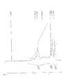
高分子反応完了後、エチルエーテル或いはヘキサン溶媒から沈澱を取り出して乾燥させ、標題のポリ(エチルマレイミド/t−ブチル−5−ノルボルネン−2−カルボキシレート/2−ヒドロキシエチル−5−ノルボルネン−2−カルボキシレート)重合体を得た。そのNMRデータを図3に示す。(収率:85%)
【0043】
実施例2:ポリ(プロピルマレイミド/t−ブチル−5−ノルボルネン−2−カルボキシレート/3−ヒドロキシプロピル−5−ノルボルネン−2−カルボキシレート)重合体(式(6))の合成
【化8】
高分子反応完了後、エチルエーテル或いはヘキサン溶媒から沈澱を取り出して乾燥させ、標題のポリ(プロピルマレイミド/t−ブチル−5−ノルボルネン−2−カルボキシレート/3−ヒドロキシプロピル−5−ノルボルネン−2−カルボキシレート)重合体を得た。そのNMRデータを図4に示す。(収率:82%)
【0044】
実施例3:ポリ(t−ブチルマレイミド/t−ブチル−ビシクロ[2、2、2]オクト−5−エン−2−カルボキシレート/2−ヒドロキシエチル−5−ノルボルネン−2−カルボキシレート)重合体(式(7))の合成
【化9】
高分子反応完了後、エチルエーテル或いはヘキサン溶媒から沈澱を取り出して乾燥させ、標題のポリ(t−ブチルマレイミド/t−ブチル−ビシクロ[2、2、2]オクト−5−エン−2−カルボキシレート/2−ヒドロキシエチル−5−ノルボルネン−2−カルボキシレート)重合体を得た。(収率:75%)
【0045】
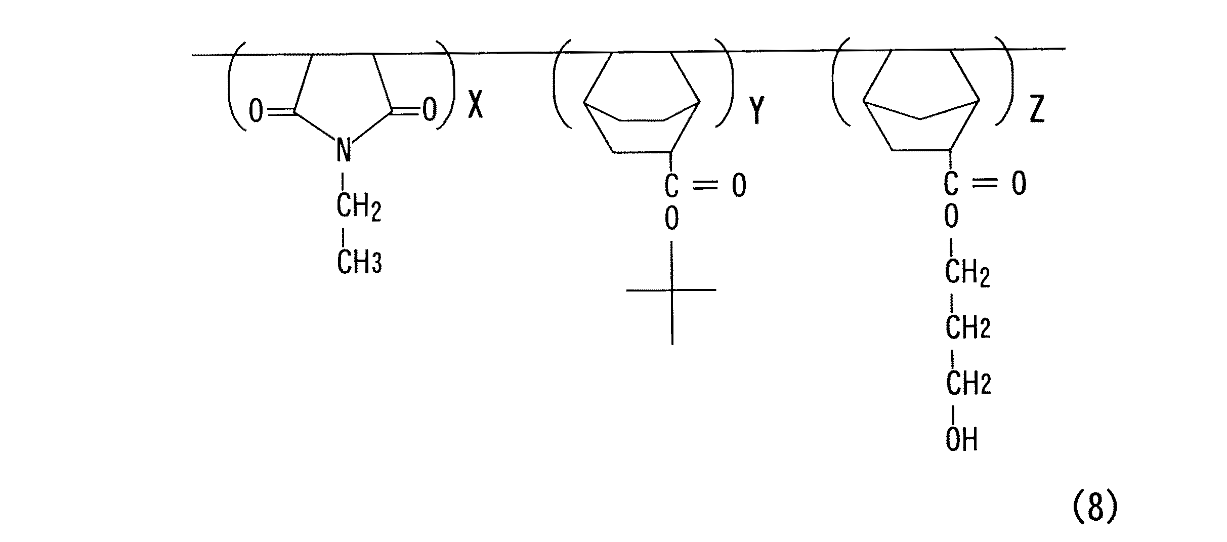
実施例4:ポリ(エチルマレイミド/t−ブチル−ビシクロ[2、2、2]オクト−5−エン−2−カルボキシレート/3−ヒドロキシプロピル−5−ノルボルネン−2−カルボキシレート)重合体(式(8))の合成
【化10】
高分子反応完了後、エチルエーテル或いはヘキサン溶媒から沈澱物を取り出して乾燥させ、標題のポリ(エチルマレイミド/t−ブチル−ビシクロ[2、2、2]オクト−5−エン−2−カルボキシレート/3−ヒドロキシプロピル−5−ノルボルネン−2−カルボキシレート)重合体を得た。そのNMRデータを図5に示す。(収率:83%)
【0046】
実施例5:ポリ(プロピルマレイミド/t−ブチル−5−ノルボルネン−2−カルボキシレート/2−ヒドロキシエチル−ビシクロ[2、2、2]オクト−5−エン−2−カルボキシレート)重合体(式(9))の合成
【化11】
高分子反応完了後、エチルエーテル或いはヘキサン溶媒から沈澱物を取り出して乾燥させ、標題のポリ(プロピルマレイミド/t−ブチル−5−ノルボルネン−2−カルボキシレート/2−ヒドロキシエチル−ビシクロ[2、2、2]オクト−5−エン−2−カルボキシレート)重合体を得た。(収率:79%)
【0047】
実施例6:ポリ(エチルマレイミド/t−ブチル−5−ノルボルネン−2−カルボキシレート/3−ヒドロキシプロピル−ビシクロ[2、2、2]オクト−5−エン−2−カルボキシレート)重合体(式(10))の合成
【化12】
【0048】
実施例7:ポリ(プロピルマレイミド/t−ブチル−ビシクロ[2、2、2]オクト−5−エン−2−カルボキシレート/3−ヒドロキシプロピル−ビシクロ[2、2、2]オクト−2−カルボキシレート)重合体(式(11))の合成
【化13】
高分子反応完了後、エチルエーテル或いはヘキサン溶媒から沈澱物を取り出して乾燥させ、標題のポリ(プロピルマレイミド/t−ブチル−ビシクロ[2、2、2]オクト−5−エン−2−カルボキシレート/2−ヒドロキシエチル−ビシクロ[2、2、2]オクト−5−エン−2−カルボキシレート)重合体を得た。(収率:78%)
【0049】
実施例8:ポリ(エチルマレイミド/t−ブチル−ビシクロ[2、2、2]オクト−5−エン−2−カルボキシレート/3−ヒドロキシプロピル−ビシクロ[2、2、2]オクト−5−エン−2−カルボキシレート)重合体(式(12))の合成
【化14】
高分子反応完了後、エチルエーテル或いはヘキサン溶媒から沈澱物を取り出して乾燥させ、標題のポリ(エチルマレイミド/t−ブチル−ビシクロ[2、2、2]オクト−5−エン−2−カルボキシレート/3−ヒドロキシプロピル−ビシクロ[2、2、2]オクト−5−エン−2−カルボキシレート)重合体を得た。(収率:75%)
【0050】
適用例1:フォトレジスト組成物の製造及びパターン形成
実施例1で合成したポリ(エチルマレイミド/t−ブチル−5−ノルボルネン−2−カルボキシレート/2−ヒドロキシエチル−5−ノルボルネン−2−カルボキシレート)重合体10gをメチル3−メトキシプロピオネート溶媒40gに溶解した後、トリフェニルスルホニウムトリフレート或いはジブチルナフチルスルホニウムトリフレート0.1〜2gを投入し、0.10μmフィルターで濾過させて得たフォトレジストをウェーハ表面にコーティングさせた後、図1および図2に示すような方法で感光膜パターンを形成した。
【0051】
適用例2:フォトレジストの製造及びパターン形成
実施例2で合成したポリ(プロピルマレイミド/t−ブチル−5−ノルボルネン−2−カルボキシレート/3−ヒドロキシプロピル−5−ノルボルネン−2−カルボキシレート)重合体10gを用い、適用例1の方法で感光膜パターンを形成した。
【0052】
適用例3:フォトレジストの製造及びパターン形成
実施例3で合成したポリ(t−ブチルマレイミド/t−ブチル−ビシクロ[2、2、2]オクト−5−エン−2−カルボキシレート/3−ヒドロキシプロピル−5−ノルボルネン−2−カルボキシレート)重合体10gを用い、適用例1の方法で感光膜パターンを形成した。
【0053】
適用例4:フォトレジストの製造及びパターン形成
実施例4で合成したポリ(エチルマレイミド/t−ブチル−ビシクロ[2、2、2]オクト−5−エン−2−カルボキシレート/3−ヒドロキシプロピル−5−ノルボルネン−2−カルボキシレート)重合体10gを用い、適用例1の方法で感光膜パターンを形成した。
【0054】
適用例5:フォトレジストの製造及びパターン形成
実施例5で合成したポリ(プロピルマレイミド/t−ブチル−5−ノルボルネン−2−カルボキシレート/2−ヒドロキシエチル−ビシクロ[2、2、2]オクト−5−エン−2−カルボキシレート)重合体10gを用い、適用例1の方法で感光膜パターンを形成した。
【0055】
適用例6:フォトレジストの製造及びパターン形成
実施例6で合成したポリ(エチルマレイミド/t−ブチル−5−ノルボルネン−2−カルボキシレート/3−ヒドロキシプロピル−ビシクロ[2、2、2]オクト−5−エン−2−カルボキシレート)重合体10gを用い、適用例1の方法で感光膜パターンを形成した。
【0056】
適用例7:フォトレジストの製造及びパターン形成
実施例7で合成したポリ(プロピルマレイミド/t−ブチル−ビシクロ[2、2、2]オクト−5−エン−2−カルボキシレート/2−ヒドロキシエチル−ビシクロ[2、2、2]オクト−5−エン−2−カルボキシレート)重合体10gを用い、適用例1の方法で感光膜パターンを形成した。
【0057】
適用例8:感光膜の製造及びパターン形成
実施例8で合成したポリ(エチルマレイミド/t−ブチル−ビシクロ[2、2、2]オクト−5−エン−2−カルボキシレート/3−ヒドロキシプロピル−ビシクロ[2、2、2]オクト−5−エン−2−カルボキシレート)重合体10gを用い、適用例1の方法で感光膜パターンを形成した。
【0058】
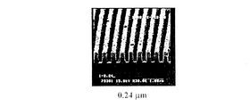
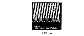
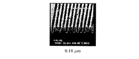
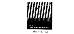
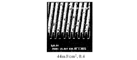
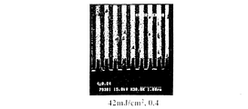
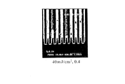
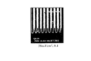
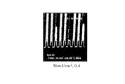
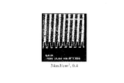
前記適用例1のフォトレジストを用い、48mJ/cm2の露光エネルギーで露光して形成したパターンの状態を図6〜図13に示し、露光エネルギーに伴う状態を図14〜図21に示した。
【0059】
【発明の効果】
以上のように、本発明に係るフォトレジストはTSIに伴う工程中、高温度の露光後ベイク工程とシリレーション工程に耐え得る耐熱性を確保することができ、ArF光源を用いるときArF工程により露光器のレンズのレンズ損傷を防止でき、さらに10mJ/cm2の少量のエネルギーにも解像の可能な化学増幅型感光膜に、O2プラズマを利用したシリレーション工程でシリコン酸化膜を形成させて耐エッチング性と耐熱性を増加させ、乾式現像工程で微細パターンを形成することができる。従って、本発明に係る重合体によるフォトレジストを利用すれば半導体素子の高集積化が可能である。
【図面の簡単な説明】
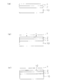
【図1】本発明に係る半導体素子のシリレーション感光膜パターンを形成する方法を示した図であり、
(a)はフォトレジストを基板上の被エッチング層上部に塗布して一次硬化した状態を示す断面図であり、
(b)は硬化させたフォトレジストを露光マスクを用いて露光した状態を示す断面図であり、
(c)は形成された露光領域を2次硬化した状態を示す断面図である。
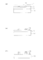
【図2】本発明に係る半導体素子のシリレーション感光膜パターンを形成する方法を示した図であり、
(d)は露光した部分にシリル化剤を分散させてシリレーション膜を形成した状態を示す断面図であり、
(e)はO2プラズマを利用してシリコン酸化膜する乾式現像工程を示す断面図であり、
(f)は被エッチング層をエッチングして微細パターンを形成した状態を示す断面図である。
【図3】ポリ(エチルマレイミド/t−ブチル−5−ノルボルネン−2−カルボキシレート/2−ヒドロキシエチル−5−ノルボルネン−2−カルボキシレート)重合体のNMRデータである。
【図4】ポリ(プロピルマレイミド/t−ブチル−5−ノルボルネン−2−カルボキシレート/3−ヒドロキシプロピル−5−ノルボルネン−2−カルボキシレート)重合体のNMRデータである。
【図5】ポリ(エチルマレイミド/t−ブチル−ビシクロ[2、2、2]オクト−5−エン−2−カルボキシレート/3−ヒドロキシプロピル−5−ノルボルネン−2−カルボキシレート)重合体のNMRデータである。
【図6】適用例1のフォトレジストを用い、48mJ/cm2の露光エネルギーで露光して形成したパターンの状態を示す図である。
【図7】適用例1のフォトレジストを用い、48mJ/cm2の露光エネルギーで露光して形成したパターンの状態を示す図である。
【図8】適用例1のフォトレジストを用い、48mJ/cm2の露光エネルギーで露光して形成したパターンの状態を示す図である。
【図9】適用例1のフォトレジストを用い、48mJ/cm2の露光エネルギーで露光して形成したパターンの状態を示す図である。
【図10】適用例1のフォトレジストを用い、48mJ/cm2の露光エネルギーで露光して形成したパターンの状態を示す図である。
【図11】適用例1のフォトレジストを用い、48mJ/cm2の露光エネルギーで露光して形成したパターンの状態を示す図である。
【図12】適用例1のフォトレジストを用い、48mJ/cm2の露光エネルギーで露光して形成したパターンの状態を示す図である。
【図13】適用例1のフォトレジストを用い、48mJ/cm2の露光エネルギーで露光して形成したパターンの状態を示す図である。
【図14】適用例1のフォトレジストを用い、露光エネルギーに伴うパターンの状態を示す図である。
【図15】適用例1のフォトレジストを用い、露光エネルギーに伴うパターンの状態を示す図である。
【図16】適用例1のフォトレジストを用い、露光エネルギーに伴うパターンの状態を示す図である。
【図17】適用例1のフォトレジストを用い、露光エネルギーに伴うパターンの状態を示す図である。
【図18】適用例1のフォトレジストを用い、露光エネルギーに伴うパターンの状態を示す図である。
【図19】適用例1のフォトレジストを用い、露光エネルギーに伴うパターンの状態を示す図である。
【図20】適用例1のフォトレジストを用い、露光エネルギーに伴うパターンの状態を示す図である。
【図21】適用例1のフォトレジストを用い、露光エネルギーに伴うパターンの状態を示す図である。
【符号の説明】
1 露光マスク
2 フォトレジスト
3 被エッチング層
10 基板
12 露光領域
14 シリレーション膜
16 シリコン酸化膜[0001]
BACKGROUND OF THE INVENTION
The present invention relates to a polymer and a method for forming a fine pattern using the same, and relates to a polymer that can be used for TSI (top surface image) and single photosensitive film resin. More specifically, the present invention can be used to form ultrafine patterns of 4G and 16G DRAMs, and a polymer that can use KrF, ArF, E-beam, EUV, ino-beam, and X-rays, and the same are used. The present invention relates to a method for forming a fine pattern.
[0002]
[Prior art]
Generally, in a semiconductor device manufacturing process, a photosensitive film pattern is used to form a semiconductor device pattern having a predetermined shape.
In order to obtain a desired photosensitive film pattern, a photoresist is applied on a semiconductor substrate, and after the applied photoresist is exposed, a developing process is performed to form a photoresist pattern on the semiconductor substrate.
In manufacturing a photosensitive film pattern using a conventional general silylation process, the photosensitive film is mainly formed of a novolac resin or a polyvinylphenol resin. Therefore, if baking is performed after exposure with an ArF light source (193 nm), an alcohol group is formed in the exposed portion. When baked and then silylated with a silylating agent such as hexameditilsilazane or tetramethylsilazane, it will have an N-Si bond.
Since such N—Si bond is weak, it reacts with R—O—H of the polymer to form R—O—Si bond. Silicon bonded to polymer is O2A silicon oxide film is formed by dry development using plasma, and the lower end portion of this portion forms a remaining pattern as it is after development.
[0003]
[Problems to be solved by the invention]
However, the method for forming a photosensitive film pattern for ArF silylation according to the prior art cannot form an ultrafine pattern of 0.10 μm L / S or less when using a KrF excimer laser, and an ArF light source is used. 10mJ / cm because the exposure lens is damaged by the high energy of ArF light.2Although exposure must be performed with the following low exposure energy, the pattern cannot be formed because the photosensitive film is not sufficiently exposed with such low energy.
[0004]
The present invention has been invented for the purpose of solving the above-mentioned conventional problems, and includes the following photoresist polymer and production method thereof, a photoresist composition containing the photoresist polymer, and a photoresist pattern. ofForming methodIt is to provide.
[0005]
[Means for Solving the Problems]
As a result of repeating numerous studies and experiments in order to solve the problems of the prior art described above, the present inventors have been accompanied by TSI by introducing an alicyclic compound into the photosensitive film resin. It is possible to ensure heat resistance that can withstand post exposure bake and silylation process, where the temperature is high during the process, and when using an ArF light source by using a chemically amplified resist, ArF light does not damage the lens of the exposure tool, and a small amount of energy (10mJ / cm2) Can be developed, and it is possible to prevent the collapse and development of the photosensitive film pattern that occurs when forming a fine pattern using an ArF (193 nm) light source, or the phenomenon of insufficient resolving power.2A silicon photosensitive film is formed by a silicidation process using plasma, the etching resistance and heat resistance are increased, and the surprising fact that a fine pattern can be formed by a dry development process is clarified and the present invention is completed. It was.
[0006]
That is, the invention described in
It is a photoresist polymer represented by the following formula (1).
[Chemical 3]
R1Represents a C1-C10 alkyl substituted on the side chain or main chain, or a benzyl group,
R2Is 1 having 1 to 10 carbon atomsClass2ClassOr 3ClassIndicates alcohol,
m and n each represent a number from 1 to 3,
X, Y and Z indicate the polymerization ratio of each monomerAnd
The ratio of X: Y: Z is 10-80: 10-80: 10-80 mol%.
[0008]
Claim 2The invention described is the photoresist polymer according to
The photoresist polymer is
Poly (ethylmaleimide / t-butyl-5-norbornene-2-carboxylate / 2-hydroxyethyl-5-norbornene-2-carboxylate),
Poly (propylmaleimide / t-butyl-5-norbornene-2-carboxylate / 3-hydroxypropyl-5-norbornene-2-carboxylate),
Poly (t-butylmaleimide / t-butyl-bicyclo [2,2,2] oct-5-ene-2-carboxylate / 2-hydroxyethyl-5-norbornene-2-carboxylate),
Poly (ethylmaleimide / t-butyl-bicyclo [2,2,2] oct-5-ene-2-carboxylate / 3-hydroxypropyl-5-norbornene-2-carboxylate),
Poly (propylmaleimide / t-butyl-5-norbornene-2-carboxylate / 2-hydroxyethyl-bicyclo [2,2,2] oct-5-ene-2-carboxylate),
Poly (ethylmaleimide / t-butyl-5-norbornene-2-carboxylate / 3-hydroxypropyl-bicyclo [2,2,2] oct-5-ene-2-carboxylate),
Poly (propylmaleimide / t-butyl-bicyclo [2,2,2] oct-5-ene-2-carboxylate / 2-hydroxyethyl-bicyclo [2,2,2] oct-5-en-2-carboxy Rate) and
Poly (ethylmaleimide / t-butyl-bicyclo [2,2,2] oct-5-ene-2-carboxylate / 3-hydroxypropyl-bicyclo [2,2,2] oct-5-en-2-carboxy The rate is selected from the group consisting of:
[0009]
Claim 3The invention described is a method for producing a photoresist polymer according to
(A) (i) a compound of the following formula (2), (ii) a compound of the following formula (3), and (iii) dissolving a compound of the following formula (4) in a polymerization organic solvent;
(B) adding a polymerization initiator to the resultant solution to induce a polymerization reaction;
(C) The method includes the step of precipitating the resultant solution and then drying the precipitate.
[Formula 4]
R1Represents a side chain or main chain substituted alkyl having 1 to 10 carbon atoms, or a benzyl group,
R2Is 1 having 1 to 10 carbon atomsClass2ClassOr 3ClassAlcohol is shown, m and n show the number of 1-3, respectively.
[0010]
Claim 4The described inventionClaim 3The method for producing a photoresist polymer according to
[0011]
Claim 5The described inventionClaim 3The method for producing a photoresist polymer as described above, wherein the polymerization organic solvent is tetrahydrofuran (THF), cyclohexane, methyl ethyl ketone, benzene, toluene, dioxane, or dimethylformamide.
[0012]
Claim 6The described inventionClaim 3The method for producing a photoresist polymer as described above, wherein the step (b) is performed in a nitrogen or argon atmosphere at a temperature of 60 to 70 ° C. for 4 to 24 hours.
[0013]
Claim 7The described invention
(I) the photoresist polymer of
(Ii) a photoacid generator;
(Iii) A photoresist composition comprising an organic solvent.
[0014]
Claim 8The described inventionClaim 7The photoresist composition according to
[0015]
Claim 9The described inventionClaim 7The photoacid generator includes diphenyliodo salt hexafluorophosphate, diphenyliodo salt hexafluoroarsenate, diphenyliodo salt hexafluoroantimonate, diphenylparamethoxyphenyl triflate, and diphenylparaffin. Toluenyl triflate, diphenyl paraisobutylphenyl triflate, diphenyl para-t-butylphenyl triflate, triphenylsulfonium hexafluorophosphate, triphenylsulfonium hexafluoroarsenate, triphenylsulfonium hexafluoroantimonate, dibutylnaphthylsulfonium triflate , And triphenylsulfonium triflate.
[0016]
Claim 10The described inventionClaim 7The photoresist composition as described above, wherein the organic solvent is ethyl-3-ethoxypropionate, ethyl lactate, methyl-3-methoxypropionate, or propylene glycol methyl ether acetate.
[0017]
Claim 11The described inventionClaim 7The photoresist composition according to
[0018]
Claim 12The described inventionClaim 7It is a photoresist composition as described, Comprising: The said organic solvent is contained in the quantity of 100 to 700 weight% of the used photoresist polymer, It is characterized by the above-mentioned.
[0019]
Claim 13The described invention is a method of forming a photoresist pattern,
(A)Claim 7Applying the photoresist composition described above to the top of the layer to be etched to form a photoresist layer;
(B) exposing the photoresist layer using exposure equipment;
(C) spraying a silylating agent on the entire surface of the resultant product;
(D) performing a dry etching process on the entire surface of the resultant product.
[0020]
Claim 14The described inventionClaim 13The method for forming a photoresist pattern according to
[0021]
Claim 15The described inventionClaim 13The method for forming a photoresist pattern according to
[0022]
Claim 16The described inventionClaim 13The method of forming a photoresist pattern according to
[0023]
Claim 17The described inventionClaim 13The method for forming a photoresist pattern according to
[0024]
Claim 18The described inventionClaim 13The method for forming a photoresist pattern according to
[0026]
DETAILED DESCRIPTION OF THE INVENTION
The above and other features of the present invention are described below.
[0027]
The present invention relates to a polymer represented by the following formula (1), and can be used not only for a single layer process but also for a photoresist for TSI.
[Chemical formula 5]
R1Represents a C1-C10 alkyl substituted on the side chain or main chain, or a benzyl group,
R2Is 1 having 1 to 10 carbon atomsClass2ClassOr 3ClassIndicates alcohol,
m and n each represent a number from 1 to 3,
X, Y and Z are polymerization ratios of the respective comonomer, and the ratio of X: Y: Z is preferably 10 to 80:10 to 80:10 to 80 mol%.
[0028]
Further, the present invention utilizes the method for producing the polymer of the formula (1), a photoresist containing the polymer of the formula (1), a solvent and a photoacid generator, and further using the photoresist. The present invention relates to a method for forming a fine pattern.
[0029]
Hereinafter, the present invention will be specifically described as follows.
The polymer of formula (1) according to the present invention comprises an alkylmaleimide represented by the following formula (2), a compound represented by the following formula (3), and a compound represented by the following formula (4) in the presence of a polymerization initiator. It can be polymerized and produced below.
[Chemical 6]
R1Represents a C1-C10 alkyl substituted on the side chain or main chain, or a benzyl group,
R2Is 1 having 1 to 10 carbon atomsClass2ClassOr 3ClassIndicates alcohol,
m and n each represent a number of 1 to 3.
[0030]
The alkylmaleimide of the formula (2) used in the present invention includes methylmaleimide, ethylmaleimide, propylmaleimide, i-propylmaleimide, n-butylmaleimide, i-butylmaleimide, t-butylmaleimide, pentylmaleimide, etc. Preferably, ethyl maleimide, propyl maleimide, or t-butyl maleimide is used.
[0031]
The compound of the formula (3) used in the present invention is preferably t-butyl-5-norbornene-2-carboxylate or t-butyl-bicyclo [2,2,2] oct-5-ene-2-carboxylate. .
[0032]
In the present invention, the compound of the formula (4) is R2Includes compounds of methyl alcohol, ethyl alcohol, propyl alcohol, butyl alcohol or pentyl alcohol. Preferably 2-hydroxyethyl-5-norbornene-2-carboxylate, 3-hydroxypropyl-5-norbornene-2-carboxylate, 2-hydroxyethyl-bicyclo [2,2,2] oct-5-ene-2 Carboxylate or 3-hydroxypropyl-bicyclo [2,2,2] oct-5-ene-2-carboxylate is used.
[0033]
According to the present invention, the alkylmaleimide of formula (2), the compound of formula (3) and the compound of formula (4) are (1-2) :( 0.5-1.5) :( 0.5-1 .5) is reacted at a molar ratio of (1) to produce a polymer.
[0034]
The polymer of the present invention can be produced by a usual polymerization method in the presence of a polymerization initiator. Examples of the polymerization method include bulk polymerization and solution polymerization. As the polymerization initiator, benzoyl peroxide, 2,2-azobisisobutyronitrile (AIBN), acetyl peroxide, lauryl peroxide, or t-butyl acetate can be used. As the polymerization solvent, tetrahydrofuran (THF), cyclohexane, methyl ethyl ketone, benzene, toluene, dioxane or dimethylformamide is used. The polymerization is carried out at a temperature of 60 to 75 ° C. for 4 to 24 hours under a nitrogen or argon atmosphere. However, it is not limited to such polymerization conditions.
[0035]
The polymer of the formula (1) produced as described above is useful for forming a fine pattern of a semiconductor element. The photoresist composition according to the present invention can be produced by mixing the polymer of the formula (1) with a solvent and a photoacid generator by a usual method.
[0036]
The photoacid generator is a sulfide or onium salt, such as diphenyliodonium hexafluorophosphate, diphenyliodonium hexafluoroarsenate, diphenyliodonium hexafluoroantimonate, diphenyl paramethoxyphenyl triflate, diphenyl paraflate. Toluenyl triflate, diphenyl paraisobutylphenyl triflate, diphenyl para-t-butylphenyl triflate, triphenylsulfonium hexafluorophosphate, triphenylsulfonium hexafluoroarsenate, triphenylsulfonium hexafluoroantimonate, dibutylnaphthylsulfonium trif One or more selected from a rate, triphenylsulfonium triflate Use.
[0037]
The photoacid generator is used in an amount of 1-20% by weight of the photoresist polymer used. This is because the sensitivity is insufficient when it is 1% or less, and the etching resistance is insufficient when it is 20% or more. As the solvent, methyl-3-methoxypropionate, ethyl lactate, ethyl-3-ethoxypropionate, methyl-3-methoxypropionate, propylene glycol methyl ether acetate can be used.
[0038]
The solvent is used in an amount of 100 to 700% based on the weight of the polymer used. A photosensitive film having a thickness of about 0.3 to 3 μm can be formed according to the amount of the solvent.
[0039]
The present invention further includes a method of forming a fine pattern using the photoresist composition. Specifically, as shown in FIGS. 1 and 2, the
[0040]
Hereinafter, the present invention will be described in detail with reference to the accompanying drawings.
1 and 2 are cross-sectional views illustrating a method of forming a silylation photosensitive film pattern of a semiconductor device according to the present invention.
First, a photoresist containing a polymer of the formula (1) is applied on the
As the silylating agent, hexamethyldisilazane, tetramethyldisilazane, dimethylaminodimethylsilane, dimethylaminoethylsilane, dimethylsilyldimethylamine, trimethylsilyldimethylamine, trimethylsilyldiethylamine, dimethylaminopentamethylsilane, or the like is used. The silylation process is performed at a temperature of 90 to 180 ° C. for about 30 to 300 seconds. After the silylation process, a silicon oxide film is formed by a dry development process using plasma in an oxygen atmosphere, the silicon oxide film is covered with an etching mask, and the etched
[0041]
【Example】
EXAMPLES Hereinafter, although this invention is demonstrated concretely based on a manufacture example and an Example, it should not be understood that the technical scope of this invention is limited to these.
[0042]
Example 1: Synthesis of poly (ethylmaleimide / t-butyl-5-norbornene-2-carboxylate / 2-hydroxyethyl-5-norbornene-2-carboxylate) polymer (formula (5))
[Chemical 7]
After completion of the polymer reaction, the precipitate was taken out from ethyl ether or hexane solvent and dried to give the title poly (ethylmaleimide / t-butyl-5-norbornene-2-carboxylate / 2-hydroxyethyl-5-norbornene-2- A carboxylate) polymer was obtained. The NMR data is shown in FIG. (Yield: 85%)
[0043]
Example 2: Synthesis of poly (propylmaleimide / t-butyl-5-norbornene-2-carboxylate / 3-hydroxypropyl-5-norbornene-2-carboxylate) polymer (formula (6))
[Chemical 8]
After completion of the polymer reaction, the precipitate was taken out from ethyl ether or hexane solvent and dried to give the title poly (propylmaleimide / t-butyl-5-norbornene-2-carboxylate / 3-hydroxypropyl-5-norbornene-2- A carboxylate) polymer was obtained. The NMR data is shown in FIG. (Yield: 82%)
[0044]
Example 3: Poly (t-butylmaleimide / t-butyl-bicyclo [2,2,2] oct-5-ene-2-carboxylate / 2-hydroxyethyl-5-norbornene-2-carboxylate) polymer Synthesis of (Formula (7))
[Chemical 9]
After completion of the polymer reaction, the precipitate was taken out from ethyl ether or hexane solvent and dried to give the title poly (t-butylmaleimide / t-butyl-bicyclo [2,2,2] oct-5-ene-2-carboxylate / 2-hydroxyethyl-5-norbornene-2-carboxylate) polymer was obtained. (Yield: 75%)
[0045]
Example 4: Poly (ethylmaleimide / t-butyl-bicyclo [2,2,2] oct-5-ene-2-carboxylate / 3-hydroxypropyl-5-norbornene-2-carboxylate) polymer (formula Synthesis of (8))
[Chemical Formula 10]
After completion of the polymer reaction, the precipitate was taken out from ethyl ether or hexane solvent and dried to give the title poly (ethylmaleimide / t-butyl-bicyclo [2,2,2] oct-5-ene-2-carboxylate / 3-hydroxypropyl-5-norbornene-2-carboxylate) polymer was obtained. The NMR data is shown in FIG. (Yield: 83%)
[0046]
Example 5: Poly (propylmaleimide / t-butyl-5-norbornene-2-carboxylate / 2-hydroxyethyl-bicyclo [2,2,2] oct-5-ene-2-carboxylate) polymer (formula Synthesis of (9))
Embedded image
After completion of the polymer reaction, the precipitate was taken out from ethyl ether or hexane solvent and dried to give the title poly (propylmaleimide / t-butyl-5-norbornene-2-carboxylate / 2-hydroxyethyl-bicyclo [2,2, 2] Oct-5-ene-2-carboxylate) polymer was obtained. (Yield: 79%)
[0047]
Example 6: Poly (ethylmaleimide / t-butyl-5-norbornene-2-carboxylate / 3-hydroxypropyl-bicyclo [2,2,2] oct-5-ene-2-carboxylate) polymer (formula Synthesis of (10))
Embedded image
[0048]
Example 7: Poly (propylmaleimide / t-butyl-bicyclo [2,2,2] oct-5-ene-2-carboxylate / 3-hydroxypropyl-bicyclo [2,2,2] oct-2-carboxy Rate) polymer (formula (11)) synthesis
Embedded image
After completion of the polymer reaction, the precipitate was taken out from ethyl ether or hexane solvent and dried to give the title poly (propylmaleimide / t-butyl-bicyclo [2,2,2] oct-5-ene-2-carboxylate / 2-Hydroxyethyl-bicyclo [2,2,2] oct-5-ene-2-carboxylate) polymer was obtained. (Yield: 78%)
[0049]
Example 8: Poly (ethylmaleimide / t-butyl-bicyclo [2,2,2] oct-5-ene-2-carboxylate / 3-hydroxypropyl-bicyclo [2,2,2] oct-5-ene -2-Carboxylate) Polymer (Formula (12))
Embedded image
After completion of the polymer reaction, the precipitate was taken out from ethyl ether or hexane solvent and dried to give the title poly (ethylmaleimide / t-butyl-bicyclo [2,2,2] oct-5-ene-2-carboxylate / A 3-hydroxypropyl-bicyclo [2,2,2] oct-5-ene-2-carboxylate) polymer was obtained. (Yield: 75%)
[0050]
Application Example 1: Production of photoresist composition and pattern formation
10 g of the poly (ethylmaleimide / t-butyl-5-norbornene-2-carboxylate / 2-hydroxyethyl-5-norbornene-2-carboxylate) polymer synthesized in Example 1 was used as a solvent for methyl 3-methoxypropionate. After dissolving in 40 g, 0.1 to 2 g of triphenylsulfonium triflate or dibutylnaphthylsulfonium triflate is added, and a photoresist obtained by filtering through a 0.10 μm filter is coated on the wafer surface. A photosensitive film pattern was formed by the method shown in FIG.
[0051]
Application Example 2: Production of photoresist and pattern formation
Using 10 g of the poly (propylmaleimide / t-butyl-5-norbornene-2-carboxylate / 3-hydroxypropyl-5-norbornene-2-carboxylate) polymer synthesized in Example 2, the method of Application Example 1 was used. A photosensitive film pattern was formed.
[0052]
Application Example 3: Production of photoresist and pattern formation
Poly (t-butylmaleimide / t-butyl-bicyclo [2,2,2] oct-5-ene-2-carboxylate / 3-hydroxypropyl-5-norbornene-2-carboxylate) synthesized in Example 3 A photosensitive film pattern was formed by the method of Application Example 1 using 10 g of the polymer.
[0053]
Application Example 4: Production of photoresist and pattern formation
Poly (ethylmaleimide / t-butyl-bicyclo [2,2,2] oct-5-ene-2-carboxylate / 3-hydroxypropyl-5-norbornene-2-carboxylate) polymer synthesized in Example 4 A photosensitive film pattern was formed by the method of Application Example 1 using 10 g.
[0054]
Application Example 5: Production of photoresist and pattern formation
Poly (propylmaleimide / t-butyl-5-norbornene-2-carboxylate / 2-hydroxyethyl-bicyclo [2,2,2] oct-5-ene-2-carboxylate) polymer synthesized in Example 5 A photosensitive film pattern was formed by the method of Application Example 1 using 10 g.
[0055]
Application Example 6: Production of photoresist and pattern formation
Poly (ethylmaleimide / t-butyl-5-norbornene-2-carboxylate / 3-hydroxypropyl-bicyclo [2,2,2] oct-5-ene-2-carboxylate) polymer synthesized in Example 6 A photosensitive film pattern was formed by the method of Application Example 1 using 10 g.
[0056]
Application Example 7: Production of photoresist and pattern formation
Poly (propylmaleimide / t-butyl-bicyclo [2,2,2] oct-5-ene-2-carboxylate / 2-hydroxyethyl-bicyclo [2,2,2] oct-5 synthesized in Example 7 A photosensitive film pattern was formed by the method of Application Example 1 using 10 g of the -en-2-carboxylate) polymer.
[0057]
Application Example 8: Production of photosensitive film and pattern formation
Poly (ethylmaleimide / t-butyl-bicyclo [2,2,2] oct-5-ene-2-carboxylate / 3-hydroxypropyl-bicyclo [2,2,2] oct-5 synthesized in Example 8 A photosensitive film pattern was formed by the method of Application Example 1 using 10 g of the -en-2-carboxylate) polymer.
[0058]
Using the photoresist of Application Example 1 above, 48 mJ / cm2The state of the pattern formed by exposing with the exposure energy of FIG. 6 is shown in FIGS. 6 to 13, and the state accompanying the exposure energy is shown in FIGS.
[0059]
【The invention's effect】
As described above, the photoresist according to the present invention can ensure heat resistance that can withstand a high temperature post-exposure baking process and a silylation process during the process accompanying TSI, and is exposed by an ArF process when using an ArF light source Can prevent damage to the lens of the container, and 10mJ / cm2A chemically amplified photosensitive film that can be resolved even with a small amount of energy.2A silicon oxide film is formed by a silylation process using plasma to increase etching resistance and heat resistance, and a fine pattern can be formed by a dry development process. Therefore, the semiconductor element can be highly integrated by using the photoresist of the polymer according to the present invention.
[Brief description of the drawings]
FIG. 1 is a view showing a method of forming a silylation photosensitive film pattern of a semiconductor device according to the present invention;
(A) is sectional drawing which shows the state which apply | coated the photoresist to the to-be-etched layer upper part on a board | substrate, and was primary-cured,
(B) is a cross-sectional view showing a state in which a cured photoresist is exposed using an exposure mask;
(C) is sectional drawing which shows the state which carried out secondary hardening of the formed exposure area | region.
FIG. 2 is a view showing a method of forming a silylation photosensitive film pattern of a semiconductor device according to the present invention;
(D) is a cross-sectional view showing a state in which a silylating agent is dispersed in an exposed portion to form a silylation film,
(E) is O2It is a cross-sectional view showing a dry development process for forming a silicon oxide film using plasma,
(F) is sectional drawing which shows the state which etched the to-be-etched layer and formed the fine pattern.
FIG. 3 is NMR data of a poly (ethylmaleimide / t-butyl-5-norbornene-2-carboxylate / 2-hydroxyethyl-5-norbornene-2-carboxylate) polymer.
FIG. 4 is NMR data of a poly (propylmaleimide / t-butyl-5-norbornene-2-carboxylate / 3-hydroxypropyl-5-norbornene-2-carboxylate) polymer.
FIG. 5: NMR of poly (ethylmaleimide / t-butyl-bicyclo [2,2,2] oct-5-ene-2-carboxylate / 3-hydroxypropyl-5-norbornene-2-carboxylate) polymer. It is data.
FIG. 6 is 48 mJ / cm using the photoresist of Application Example 1.2It is a figure which shows the state of the pattern formed by exposing with the exposure energy of.
7 is 48 mJ / cm using the photoresist of Application Example 1. FIG.2It is a figure which shows the state of the pattern formed by exposing with the exposure energy of.
FIG. 8 shows 48 mJ / cm using the photoresist of Application Example 1.2It is a figure which shows the state of the pattern formed by exposing with the exposure energy of.
9 is 48 mJ / cm using the photoresist of Application Example 1. FIG.2It is a figure which shows the state of the pattern formed by exposing with the exposure energy of.
FIG. 10 is 48 mJ / cm using the photoresist of Application Example 1.2It is a figure which shows the state of the pattern formed by exposing with the exposure energy of.
11 is 48 mJ / cm using the photoresist of Application Example 1. FIG.2It is a figure which shows the state of the pattern formed by exposing with the exposure energy of.
FIG. 12 shows 48 mJ / cm using the photoresist of Application Example 1.2It is a figure which shows the state of the pattern formed by exposing with the exposure energy of.
13 is 48 mJ / cm using the photoresist of Application Example 1. FIG.2It is a figure which shows the state of the pattern formed by exposing with the exposure energy of.
FIG. 14 is a diagram showing a pattern state associated with exposure energy using the photoresist of Application Example 1;
15 is a diagram showing a pattern state according to exposure energy using the photoresist of Application Example 1. FIG.
FIG. 16 is a diagram showing a pattern state associated with exposure energy using the photoresist of Application Example 1;
FIG. 17 is a diagram showing a pattern state according to exposure energy using the photoresist of Application Example 1;
FIG. 18 is a diagram showing a pattern state according to exposure energy using the photoresist of Application Example 1;
FIG. 19 is a diagram showing a pattern state associated with exposure energy using the photoresist of Application Example 1;
FIG. 20 is a diagram showing a pattern state according to exposure energy using the photoresist of Application Example 1;
FIG. 21 is a diagram showing a pattern state according to exposure energy using the photoresist of Application Example 1;
[Explanation of symbols]
1 Exposure mask
2 photoresist
3 Layer to be etched
10 Substrate
12 Exposure area
14 Silylation membrane
16 Silicon oxide film
Claims (18)
R1は側鎖又は主鎖に置換された炭素数1〜10のアルキル、又はベンジル基を示し、
R2は炭素数1〜10の1級、2級或いは3級アルコールを示し、
m及びnはそれぞれ1〜3の数を示し、
X、Y及びZは各単量体の重合比を示し、
X:Y:Zの比は10〜80:10〜80:10〜80モル%である。 A photoresist polymer represented by the following formula (1).
R 1 represents a C 1-10 alkyl substituted on the side chain or main chain, or a benzyl group,
R 2 represents a primary, secondary or tertiary alcohols having 1 to 10 carbon atoms,
m and n each represent a number from 1 to 3,
X, Y and Z indicates a polymerization ratio of each monomer,
The ratio of X: Y: Z is 10-80: 10-80: 10-80 mol%.
ポリ(エチルマレイミド/t−ブチル−5−ノルボルネン−2−カルボキシレート/2−ヒドロキシエチル−5−ノルボルネン−2−カルボキシレート)、
ポリ(プロピルマレイミド/t−ブチル−5−ノルボルネン−2−カルボキシレート/3−ヒドロキシプロピル−5−ノルボルネン−2−カルボキシレート)、
ポリ(t−ブチルマレイミド/t−ブチル−ビシクロ[2、2、2]オクト−5−エン−2−カルボキシレート/2−ヒドロキシエチル−5−ノルボルネン−2−カルボキシレート)、
ポリ(エチルマレイミド/t−ブチル−ビシクロ[2、2、2]オクト−5−エン−2−カルボキシレート/3−ヒドロキシプロピル−5−ノルボルネン−2−カルボキシレート)、
ポリ(プロピルマレイミド/t−ブチル−5−ノルボルネン−2−カルボキシレート/2−ヒドロキシエチル−ビシクロ[2、2、2]オクト−5−エン−2−カルボキシレート)、
ポリ(エチルマレイミド/t−ブチル−5−ノルボルネン−2−カルボキシレート/3−ヒドロキシプロピル−ビシクロ[2、2、2]オクト−5−エン−2−カルボキシレート)、
ポリ(プロピルマレイミド/t−ブチル−ビシクロ[2、2、2]オクト−5−エン−2−カルボキシレート/2−ヒドロキシエチル−ビシクロ[2、2、2]オクト−5−エン−2−カルボキシレート)、及び
ポリ(エチルマレイミド/t−ブチル−ビシクロ[2、2、2]オクト−5−エン−2−カルボキシレート/3−ヒドロキシプロピル−ビシクロ[2、2、2]オクト−5−エン−2−カルボキシレート)からなる群から選択されたことを特徴とする請求項1記載のフォトレジスト重合体。The photoresist polymer is poly (ethylmaleimide / t-butyl-5-norbornene-2-carboxylate / 2-hydroxyethyl-5-norbornene-2-carboxylate),
Poly (propylmaleimide / t-butyl-5-norbornene-2-carboxylate / 3-hydroxypropyl-5-norbornene-2-carboxylate),
Poly (t-butylmaleimide / t-butyl-bicyclo [2,2,2] oct-5-ene-2-carboxylate / 2-hydroxyethyl-5-norbornene-2-carboxylate),
Poly (ethylmaleimide / t-butyl-bicyclo [2,2,2] oct-5-ene-2-carboxylate / 3-hydroxypropyl-5-norbornene-2-carboxylate),
Poly (propylmaleimide / t-butyl-5-norbornene-2-carboxylate / 2-hydroxyethyl-bicyclo [2,2,2] oct-5-ene-2-carboxylate),
Poly (ethylmaleimide / t-butyl-5-norbornene-2-carboxylate / 3-hydroxypropyl-bicyclo [2,2,2] oct-5-ene-2-carboxylate),
Poly (propylmaleimide / t-butyl-bicyclo [2,2,2] oct-5-ene-2-carboxylate / 2-hydroxyethyl-bicyclo [2,2,2] oct-5-en-2-carboxy Rate), and poly (ethylmaleimide / t-butyl-bicyclo [2,2,2] oct-5-ene-2-carboxylate / 3-hydroxypropyl-bicyclo [2,2,2] oct-5-ene The photoresist polymer according to claim 1, which is selected from the group consisting of 2-carboxylate).
(a)(i)下記式(2)の化合物と、(ii)下記式(3)の化合物と、(iii)下記式(4)の化合物を重合有機溶媒に溶解する段階と、
(b)前記結果物溶液に重合開始剤を添加して重合反応を誘導する段階と、
(c)前記結果物溶液を沈澱させた後、前記沈澱物を乾燥する段階を含むことを特徴とするフォトレジスト重合体の製造方法。
R1は側鎖又は主鎖置換された炭素数1〜10のアルキル、又はベンジル基を示し、
R2は炭素数1〜10の1級、2級或いは3級アルコールを示し、m及びnはそれぞれ1〜3の数を示す。A method for producing a photoresist polymer according to claim 1,
(A) (i) a compound of the following formula (2), (ii) a compound of the following formula (3), and (iii) dissolving a compound of the following formula (4) in a polymerization organic solvent;
(B) adding a polymerization initiator to the resultant solution to induce a polymerization reaction;
(C) A method for producing a photoresist polymer, comprising: precipitating the resultant solution; and drying the precipitate.
R 1 represents a side chain or main chain substituted alkyl having 1 to 10 carbon atoms, or a benzyl group;
R 2 represents a primary, secondary or tertiary alcohols having 1 to 10 carbon atoms, m and n represents the number of each 1-3.
(ii)光酸発生剤と、
(iii)有機溶媒とを含むことを特徴とするフォトレジスト組成物。(I) the photoresist polymer of claim 1;
(Ii) a photoacid generator;
(Iii) A photoresist composition comprising an organic solvent.
(b)露光装備を利用して前記フォトレジスト層を露光する段階と、
(c)前記結果物全面にシリル化剤を噴射する段階と、
(d)前記結果物全面に対し、乾式エッチング工程を行う段階とを含むことを特徴とするフォトレジストパターンの形成方法。(A) applying the photoresist composition according to claim 7 to the top of the layer to be etched to form a photoresist layer;
(B) exposing the photoresist layer using exposure equipment;
(C) spraying a silylating agent on the entire surface of the resultant product;
And (d) performing a dry etching process on the entire surface of the resultant product, and forming a photoresist pattern.
Applications Claiming Priority (2)
| Application Number | Priority Date | Filing Date | Title |
|---|---|---|---|
| KR1019980016222A KR100376984B1 (en) | 1998-04-30 | 1998-04-30 | Photoresist polymer and method for forming micropattern by using the same |
| KR1998P-16222 | 1998-04-30 |
Publications (3)
| Publication Number | Publication Date |
|---|---|
| JPH11349637A JPH11349637A (en) | 1999-12-21 |
| JPH11349637A5 JPH11349637A5 (en) | 2005-08-25 |
| JP4028131B2 true JP4028131B2 (en) | 2007-12-26 |
Family
ID=19537081
Family Applications (1)
| Application Number | Title | Priority Date | Filing Date |
|---|---|---|---|
| JP12538199A Expired - Fee Related JP4028131B2 (en) | 1998-04-30 | 1999-04-30 | Photoresist polymer and method for producing the same, photoresist composition, and method for forming photoresist pattern |
Country Status (7)
| Country | Link |
|---|---|
| US (1) | US6225020B1 (en) |
| JP (1) | JP4028131B2 (en) |
| KR (1) | KR100376984B1 (en) |
| CN (1) | CN1146602C (en) |
| DE (1) | DE19919795A1 (en) |
| GB (1) | GB2336846B (en) |
| TW (1) | TW491861B (en) |
Families Citing this family (392)
| Publication number | Priority date | Publication date | Assignee | Title |
|---|---|---|---|---|
| US6808859B1 (en) * | 1996-12-31 | 2004-10-26 | Hyundai Electronics Industries Co., Ltd. | ArF photoresist copolymers |
| KR100321080B1 (en) | 1997-12-29 | 2002-11-22 | 주식회사 하이닉스반도체 | Copolymer resin, method for preparing the same, and photoresist using the same |
| KR20000015014A (en) | 1998-08-26 | 2000-03-15 | 김영환 | New photoresist monomer, polymer, and photoresist compound |
| JP3587743B2 (en) | 1998-08-26 | 2004-11-10 | 株式会社ハイニックスセミコンダクター | A photoresist monomer and a method for producing the same, a photoresist copolymer and a method for producing the same, a photoresist composition, a method for forming a photoresist pattern, and a semiconductor device. |
| US6569971B2 (en) | 1998-08-27 | 2003-05-27 | Hyundai Electronics Industries Co., Ltd. | Polymers for photoresist and photoresist compositions using the same |
| TWI234051B (en) * | 1998-10-14 | 2005-06-11 | Clariant Int Ltd | A mixed solvent system for positive photoresists |
| KR20000056355A (en) * | 1999-02-19 | 2000-09-15 | 김영환 | Photoresist composition having superior characteristics in the presence of high concentration of amine |
| JP4469080B2 (en) * | 2000-12-13 | 2010-05-26 | 信越化学工業株式会社 | Novel tertiary alcohol compounds having an alicyclic structure |
| US6946523B2 (en) | 2001-02-07 | 2005-09-20 | Henkel Corporation | Heterobifunctional monomers and uses therefor |
| US6423780B1 (en) * | 2001-02-07 | 2002-07-23 | Loctite | Heterobifunctional monomers and uses therefor |
| US6521731B2 (en) * | 2001-02-07 | 2003-02-18 | Henkel Loctite Corporation | Radical polymerizable compositions containing polycyclic olefins |
| KR20020088581A (en) * | 2001-05-18 | 2002-11-29 | 인더스트리얼 테크놀로지 리써치 인스티튜트 | Silicon-containing copolymer and photosensitive resin composition containing the same |
| US7138218B2 (en) * | 2001-12-18 | 2006-11-21 | Hynix Semiconductor Inc. | Process for forming an ultra fine pattern using a bottom anti-reflective coating film containing an acid generator |
| KR100415091B1 (en) * | 2002-03-26 | 2004-01-13 | 주식회사 하이닉스반도체 | method for manufacturing fine pattern |
| JP4222306B2 (en) * | 2002-09-30 | 2009-02-12 | 日本ゼオン株式会社 | Positive-type radiation-sensitive resin composition, resin pattern film and method for forming the same, and use of resin pattern film |
| US7338742B2 (en) * | 2003-10-08 | 2008-03-04 | Hynix Semiconductor Inc. | Photoresist polymer and photoresist composition containing the same |
| US7270937B2 (en) * | 2003-10-17 | 2007-09-18 | Hynix Semiconductor Inc. | Over-coating composition for photoresist and process for forming photoresist pattern using the same |
| KR100680405B1 (en) * | 2003-11-19 | 2007-02-08 | 주식회사 하이닉스반도체 | Photoresist composition for EV and photoresist pattern forming method using same |
| US7534548B2 (en) * | 2005-06-02 | 2009-05-19 | Hynix Semiconductor Inc. | Polymer for immersion lithography and photoresist composition |
| KR100694412B1 (en) * | 2006-02-24 | 2007-03-12 | 주식회사 하이닉스반도체 | Micro pattern formation method of semiconductor device |
| US7745339B2 (en) * | 2006-02-24 | 2010-06-29 | Hynix Semiconductor Inc. | Method for forming fine pattern of semiconductor device |
| US8313876B2 (en) * | 2006-07-20 | 2012-11-20 | Hynix Semiconductor Inc. | Exposure mask and method for manufacturing semiconductor device using the same |
| KR100849800B1 (en) * | 2006-07-20 | 2008-07-31 | 주식회사 하이닉스반도체 | Exposure mask and method of manufacturing semiconductor device using same |
| US7959818B2 (en) | 2006-09-12 | 2011-06-14 | Hynix Semiconductor Inc. | Method for forming a fine pattern of a semiconductor device |
| US7790357B2 (en) * | 2006-09-12 | 2010-09-07 | Hynix Semiconductor Inc. | Method of forming fine pattern of semiconductor device |
| KR100861173B1 (en) * | 2006-12-01 | 2008-09-30 | 주식회사 하이닉스반도체 | Pattern Forming Method of Semiconductor Device Using Immersion Exposure Process |
| KR20080057562A (en) * | 2006-12-20 | 2008-06-25 | 주식회사 하이닉스반도체 | Method of forming fine pattern of semiconductor device |
| KR100919564B1 (en) * | 2007-06-29 | 2009-10-01 | 주식회사 하이닉스반도체 | Method for Forming Fine Pattern of Semiconductor Device |
| KR100876816B1 (en) * | 2007-06-29 | 2009-01-07 | 주식회사 하이닉스반도체 | Method of forming fine pattern of semiconductor device |
| KR101249681B1 (en) | 2008-01-23 | 2013-04-05 | 주식회사 엘지화학 | binder resin and photosensitive resin composition comprising the same and column Spacer made by the photosensitive resin composition |
| KR101037528B1 (en) * | 2008-10-16 | 2011-05-26 | 주식회사 하이닉스반도체 | Method for pattern formation of semiconductor device |
| US10378106B2 (en) | 2008-11-14 | 2019-08-13 | Asm Ip Holding B.V. | Method of forming insulation film by modified PEALD |
| US9394608B2 (en) | 2009-04-06 | 2016-07-19 | Asm America, Inc. | Semiconductor processing reactor and components thereof |
| US8802201B2 (en) | 2009-08-14 | 2014-08-12 | Asm America, Inc. | Systems and methods for thin-film deposition of metal oxides using excited nitrogen-oxygen species |
| US9312155B2 (en) | 2011-06-06 | 2016-04-12 | Asm Japan K.K. | High-throughput semiconductor-processing apparatus equipped with multiple dual-chamber modules |
| US10364496B2 (en) | 2011-06-27 | 2019-07-30 | Asm Ip Holding B.V. | Dual section module having shared and unshared mass flow controllers |
| US10854498B2 (en) | 2011-07-15 | 2020-12-01 | Asm Ip Holding B.V. | Wafer-supporting device and method for producing same |
| US20130023129A1 (en) | 2011-07-20 | 2013-01-24 | Asm America, Inc. | Pressure transmitter for a semiconductor processing environment |
| US9017481B1 (en) | 2011-10-28 | 2015-04-28 | Asm America, Inc. | Process feed management for semiconductor substrate processing |
| US9659799B2 (en) | 2012-08-28 | 2017-05-23 | Asm Ip Holding B.V. | Systems and methods for dynamic semiconductor process scheduling |
| US10714315B2 (en) | 2012-10-12 | 2020-07-14 | Asm Ip Holdings B.V. | Semiconductor reaction chamber showerhead |
| US20160376700A1 (en) | 2013-02-01 | 2016-12-29 | Asm Ip Holding B.V. | System for treatment of deposition reactor |
| US9484191B2 (en) | 2013-03-08 | 2016-11-01 | Asm Ip Holding B.V. | Pulsed remote plasma method and system |
| US9589770B2 (en) | 2013-03-08 | 2017-03-07 | Asm Ip Holding B.V. | Method and systems for in-situ formation of intermediate reactive species |
| US9240412B2 (en) | 2013-09-27 | 2016-01-19 | Asm Ip Holding B.V. | Semiconductor structure and device and methods of forming same using selective epitaxial process |
| US10683571B2 (en) | 2014-02-25 | 2020-06-16 | Asm Ip Holding B.V. | Gas supply manifold and method of supplying gases to chamber using same |
| US10167557B2 (en) | 2014-03-18 | 2019-01-01 | Asm Ip Holding B.V. | Gas distribution system, reactor including the system, and methods of using the same |
| US11015245B2 (en) | 2014-03-19 | 2021-05-25 | Asm Ip Holding B.V. | Gas-phase reactor and system having exhaust plenum and components thereof |
| US10858737B2 (en) | 2014-07-28 | 2020-12-08 | Asm Ip Holding B.V. | Showerhead assembly and components thereof |
| US9890456B2 (en) | 2014-08-21 | 2018-02-13 | Asm Ip Holding B.V. | Method and system for in situ formation of gas-phase compounds |
| US9657845B2 (en) | 2014-10-07 | 2017-05-23 | Asm Ip Holding B.V. | Variable conductance gas distribution apparatus and method |
| US10941490B2 (en) | 2014-10-07 | 2021-03-09 | Asm Ip Holding B.V. | Multiple temperature range susceptor, assembly, reactor and system including the susceptor, and methods of using the same |
| KR102263121B1 (en) | 2014-12-22 | 2021-06-09 | 에이에스엠 아이피 홀딩 비.브이. | Semiconductor device and manufacuring method thereof |
| US10529542B2 (en) | 2015-03-11 | 2020-01-07 | Asm Ip Holdings B.V. | Cross-flow reactor and method |
| US10276355B2 (en) | 2015-03-12 | 2019-04-30 | Asm Ip Holding B.V. | Multi-zone reactor, system including the reactor, and method of using the same |
| US10458018B2 (en) | 2015-06-26 | 2019-10-29 | Asm Ip Holding B.V. | Structures including metal carbide material, devices including the structures, and methods of forming same |
| US10600673B2 (en) | 2015-07-07 | 2020-03-24 | Asm Ip Holding B.V. | Magnetic susceptor to baseplate seal |
| US10083836B2 (en) | 2015-07-24 | 2018-09-25 | Asm Ip Holding B.V. | Formation of boron-doped titanium metal films with high work function |
| US9960072B2 (en) | 2015-09-29 | 2018-05-01 | Asm Ip Holding B.V. | Variable adjustment for precise matching of multiple chamber cavity housings |
| US10211308B2 (en) | 2015-10-21 | 2019-02-19 | Asm Ip Holding B.V. | NbMC layers |
| US10322384B2 (en) | 2015-11-09 | 2019-06-18 | Asm Ip Holding B.V. | Counter flow mixer for process chamber |
| US11139308B2 (en) | 2015-12-29 | 2021-10-05 | Asm Ip Holding B.V. | Atomic layer deposition of III-V compounds to form V-NAND devices |
| US10468251B2 (en) | 2016-02-19 | 2019-11-05 | Asm Ip Holding B.V. | Method for forming spacers using silicon nitride film for spacer-defined multiple patterning |
| US10529554B2 (en) | 2016-02-19 | 2020-01-07 | Asm Ip Holding B.V. | Method for forming silicon nitride film selectively on sidewalls or flat surfaces of trenches |
| US10501866B2 (en) | 2016-03-09 | 2019-12-10 | Asm Ip Holding B.V. | Gas distribution apparatus for improved film uniformity in an epitaxial system |
| US10343920B2 (en) | 2016-03-18 | 2019-07-09 | Asm Ip Holding B.V. | Aligned carbon nanotubes |
| US9892913B2 (en) | 2016-03-24 | 2018-02-13 | Asm Ip Holding B.V. | Radial and thickness control via biased multi-port injection settings |
| US10190213B2 (en) | 2016-04-21 | 2019-01-29 | Asm Ip Holding B.V. | Deposition of metal borides |
| US10865475B2 (en) | 2016-04-21 | 2020-12-15 | Asm Ip Holding B.V. | Deposition of metal borides and silicides |
| US10367080B2 (en) | 2016-05-02 | 2019-07-30 | Asm Ip Holding B.V. | Method of forming a germanium oxynitride film |
| US10032628B2 (en) | 2016-05-02 | 2018-07-24 | Asm Ip Holding B.V. | Source/drain performance through conformal solid state doping |
| KR102592471B1 (en) | 2016-05-17 | 2023-10-20 | 에이에스엠 아이피 홀딩 비.브이. | Method of forming metal interconnection and method of fabricating semiconductor device using the same |
| US11453943B2 (en) | 2016-05-25 | 2022-09-27 | Asm Ip Holding B.V. | Method for forming carbon-containing silicon/metal oxide or nitride film by ALD using silicon precursor and hydrocarbon precursor |
| US10388509B2 (en) | 2016-06-28 | 2019-08-20 | Asm Ip Holding B.V. | Formation of epitaxial layers via dislocation filtering |
| US10612137B2 (en) | 2016-07-08 | 2020-04-07 | Asm Ip Holdings B.V. | Organic reactants for atomic layer deposition |
| US9859151B1 (en) | 2016-07-08 | 2018-01-02 | Asm Ip Holding B.V. | Selective film deposition method to form air gaps |
| US10714385B2 (en) | 2016-07-19 | 2020-07-14 | Asm Ip Holding B.V. | Selective deposition of tungsten |
| US10381226B2 (en) | 2016-07-27 | 2019-08-13 | Asm Ip Holding B.V. | Method of processing substrate |
| US9812320B1 (en) | 2016-07-28 | 2017-11-07 | Asm Ip Holding B.V. | Method and apparatus for filling a gap |
| US9887082B1 (en) | 2016-07-28 | 2018-02-06 | Asm Ip Holding B.V. | Method and apparatus for filling a gap |
| US10395919B2 (en) | 2016-07-28 | 2019-08-27 | Asm Ip Holding B.V. | Method and apparatus for filling a gap |
| KR102532607B1 (en) | 2016-07-28 | 2023-05-15 | 에이에스엠 아이피 홀딩 비.브이. | Substrate processing apparatus and method of operating the same |
| US10410943B2 (en) | 2016-10-13 | 2019-09-10 | Asm Ip Holding B.V. | Method for passivating a surface of a semiconductor and related systems |
| US10643826B2 (en) | 2016-10-26 | 2020-05-05 | Asm Ip Holdings B.V. | Methods for thermally calibrating reaction chambers |
| US11532757B2 (en) | 2016-10-27 | 2022-12-20 | Asm Ip Holding B.V. | Deposition of charge trapping layers |
| US10714350B2 (en) | 2016-11-01 | 2020-07-14 | ASM IP Holdings, B.V. | Methods for forming a transition metal niobium nitride film on a substrate by atomic layer deposition and related semiconductor device structures |
| US10435790B2 (en) | 2016-11-01 | 2019-10-08 | Asm Ip Holding B.V. | Method of subatmospheric plasma-enhanced ALD using capacitively coupled electrodes with narrow gap |
| US10643904B2 (en) | 2016-11-01 | 2020-05-05 | Asm Ip Holdings B.V. | Methods for forming a semiconductor device and related semiconductor device structures |
| US10229833B2 (en) | 2016-11-01 | 2019-03-12 | Asm Ip Holding B.V. | Methods for forming a transition metal nitride film on a substrate by atomic layer deposition and related semiconductor device structures |
| US10134757B2 (en) | 2016-11-07 | 2018-11-20 | Asm Ip Holding B.V. | Method of processing a substrate and a device manufactured by using the method |
| KR102546317B1 (en) | 2016-11-15 | 2023-06-21 | 에이에스엠 아이피 홀딩 비.브이. | Gas supply unit and substrate processing apparatus including the same |
| US10340135B2 (en) | 2016-11-28 | 2019-07-02 | Asm Ip Holding B.V. | Method of topologically restricted plasma-enhanced cyclic deposition of silicon or metal nitride |
| KR102762543B1 (en) | 2016-12-14 | 2025-02-05 | 에이에스엠 아이피 홀딩 비.브이. | Substrate processing apparatus |
| US11447861B2 (en) | 2016-12-15 | 2022-09-20 | Asm Ip Holding B.V. | Sequential infiltration synthesis apparatus and a method of forming a patterned structure |
| US11581186B2 (en) | 2016-12-15 | 2023-02-14 | Asm Ip Holding B.V. | Sequential infiltration synthesis apparatus |
| KR102700194B1 (en) | 2016-12-19 | 2024-08-28 | 에이에스엠 아이피 홀딩 비.브이. | Substrate processing apparatus |
| US10269558B2 (en) | 2016-12-22 | 2019-04-23 | Asm Ip Holding B.V. | Method of forming a structure on a substrate |
| US10867788B2 (en) | 2016-12-28 | 2020-12-15 | Asm Ip Holding B.V. | Method of forming a structure on a substrate |
| US11390950B2 (en) | 2017-01-10 | 2022-07-19 | Asm Ip Holding B.V. | Reactor system and method to reduce residue buildup during a film deposition process |
| US10655221B2 (en) | 2017-02-09 | 2020-05-19 | Asm Ip Holding B.V. | Method for depositing oxide film by thermal ALD and PEALD |
| US10468261B2 (en) | 2017-02-15 | 2019-11-05 | Asm Ip Holding B.V. | Methods for forming a metallic film on a substrate by cyclical deposition and related semiconductor device structures |
| US10283353B2 (en) | 2017-03-29 | 2019-05-07 | Asm Ip Holding B.V. | Method of reforming insulating film deposited on substrate with recess pattern |
| US10529563B2 (en) | 2017-03-29 | 2020-01-07 | Asm Ip Holdings B.V. | Method for forming doped metal oxide films on a substrate by cyclical deposition and related semiconductor device structures |
| KR102457289B1 (en) | 2017-04-25 | 2022-10-21 | 에이에스엠 아이피 홀딩 비.브이. | Method for depositing a thin film and manufacturing a semiconductor device |
| US10770286B2 (en) | 2017-05-08 | 2020-09-08 | Asm Ip Holdings B.V. | Methods for selectively forming a silicon nitride film on a substrate and related semiconductor device structures |
| US10446393B2 (en) | 2017-05-08 | 2019-10-15 | Asm Ip Holding B.V. | Methods for forming silicon-containing epitaxial layers and related semiconductor device structures |
| US10892156B2 (en) | 2017-05-08 | 2021-01-12 | Asm Ip Holding B.V. | Methods for forming a silicon nitride film on a substrate and related semiconductor device structures |
| US10504742B2 (en) | 2017-05-31 | 2019-12-10 | Asm Ip Holding B.V. | Method of atomic layer etching using hydrogen plasma |
| US10886123B2 (en) | 2017-06-02 | 2021-01-05 | Asm Ip Holding B.V. | Methods for forming low temperature semiconductor layers and related semiconductor device structures |
| US12040200B2 (en) | 2017-06-20 | 2024-07-16 | Asm Ip Holding B.V. | Semiconductor processing apparatus and methods for calibrating a semiconductor processing apparatus |
| US11306395B2 (en) | 2017-06-28 | 2022-04-19 | Asm Ip Holding B.V. | Methods for depositing a transition metal nitride film on a substrate by atomic layer deposition and related deposition apparatus |
| US10685834B2 (en) | 2017-07-05 | 2020-06-16 | Asm Ip Holdings B.V. | Methods for forming a silicon germanium tin layer and related semiconductor device structures |
| KR20190009245A (en) | 2017-07-18 | 2019-01-28 | 에이에스엠 아이피 홀딩 비.브이. | Methods for forming a semiconductor device structure and related semiconductor device structures |
| US10541333B2 (en) | 2017-07-19 | 2020-01-21 | Asm Ip Holding B.V. | Method for depositing a group IV semiconductor and related semiconductor device structures |
| US11018002B2 (en) | 2017-07-19 | 2021-05-25 | Asm Ip Holding B.V. | Method for selectively depositing a Group IV semiconductor and related semiconductor device structures |
| US11374112B2 (en) | 2017-07-19 | 2022-06-28 | Asm Ip Holding B.V. | Method for depositing a group IV semiconductor and related semiconductor device structures |
| US10605530B2 (en) | 2017-07-26 | 2020-03-31 | Asm Ip Holding B.V. | Assembly of a liner and a flange for a vertical furnace as well as the liner and the vertical furnace |
| US10590535B2 (en) | 2017-07-26 | 2020-03-17 | Asm Ip Holdings B.V. | Chemical treatment, deposition and/or infiltration apparatus and method for using the same |
| US10312055B2 (en) | 2017-07-26 | 2019-06-04 | Asm Ip Holding B.V. | Method of depositing film by PEALD using negative bias |
| TWI815813B (en) | 2017-08-04 | 2023-09-21 | 荷蘭商Asm智慧財產控股公司 | Showerhead assembly for distributing a gas within a reaction chamber |
| US10770336B2 (en) | 2017-08-08 | 2020-09-08 | Asm Ip Holding B.V. | Substrate lift mechanism and reactor including same |
| US10692741B2 (en) | 2017-08-08 | 2020-06-23 | Asm Ip Holdings B.V. | Radiation shield |
| US11769682B2 (en) | 2017-08-09 | 2023-09-26 | Asm Ip Holding B.V. | Storage apparatus for storing cassettes for substrates and processing apparatus equipped therewith |
| US11139191B2 (en) | 2017-08-09 | 2021-10-05 | Asm Ip Holding B.V. | Storage apparatus for storing cassettes for substrates and processing apparatus equipped therewith |
| US10249524B2 (en) | 2017-08-09 | 2019-04-02 | Asm Ip Holding B.V. | Cassette holder assembly for a substrate cassette and holding member for use in such assembly |
| USD900036S1 (en) | 2017-08-24 | 2020-10-27 | Asm Ip Holding B.V. | Heater electrical connector and adapter |
| US11830730B2 (en) | 2017-08-29 | 2023-11-28 | Asm Ip Holding B.V. | Layer forming method and apparatus |
| KR102491945B1 (en) | 2017-08-30 | 2023-01-26 | 에이에스엠 아이피 홀딩 비.브이. | Substrate processing apparatus |
| US11056344B2 (en) | 2017-08-30 | 2021-07-06 | Asm Ip Holding B.V. | Layer forming method |
| US11295980B2 (en) | 2017-08-30 | 2022-04-05 | Asm Ip Holding B.V. | Methods for depositing a molybdenum metal film over a dielectric surface of a substrate by a cyclical deposition process and related semiconductor device structures |
| KR102401446B1 (en) | 2017-08-31 | 2022-05-24 | 에이에스엠 아이피 홀딩 비.브이. | Substrate processing apparatus |
| US10607895B2 (en) | 2017-09-18 | 2020-03-31 | Asm Ip Holdings B.V. | Method for forming a semiconductor device structure comprising a gate fill metal |
| KR102630301B1 (en) | 2017-09-21 | 2024-01-29 | 에이에스엠 아이피 홀딩 비.브이. | Method of sequential infiltration synthesis treatment of infiltrateable material and structures and devices formed using same |
| US10844484B2 (en) | 2017-09-22 | 2020-11-24 | Asm Ip Holding B.V. | Apparatus for dispensing a vapor phase reactant to a reaction chamber and related methods |
| US10658205B2 (en) | 2017-09-28 | 2020-05-19 | Asm Ip Holdings B.V. | Chemical dispensing apparatus and methods for dispensing a chemical to a reaction chamber |
| US10403504B2 (en) | 2017-10-05 | 2019-09-03 | Asm Ip Holding B.V. | Method for selectively depositing a metallic film on a substrate |
| US10319588B2 (en) | 2017-10-10 | 2019-06-11 | Asm Ip Holding B.V. | Method for depositing a metal chalcogenide on a substrate by cyclical deposition |
| US10923344B2 (en) | 2017-10-30 | 2021-02-16 | Asm Ip Holding B.V. | Methods for forming a semiconductor structure and related semiconductor structures |
| US10910262B2 (en) | 2017-11-16 | 2021-02-02 | Asm Ip Holding B.V. | Method of selectively depositing a capping layer structure on a semiconductor device structure |
| KR102443047B1 (en) | 2017-11-16 | 2022-09-14 | 에이에스엠 아이피 홀딩 비.브이. | Substrate processing apparatus method and apparatus manufactured thereby |
| US11022879B2 (en) | 2017-11-24 | 2021-06-01 | Asm Ip Holding B.V. | Method of forming an enhanced unexposed photoresist layer |
| WO2019103610A1 (en) | 2017-11-27 | 2019-05-31 | Asm Ip Holding B.V. | Apparatus including a clean mini environment |
| WO2019103613A1 (en) | 2017-11-27 | 2019-05-31 | Asm Ip Holding B.V. | A storage device for storing wafer cassettes for use with a batch furnace |
| US10290508B1 (en) | 2017-12-05 | 2019-05-14 | Asm Ip Holding B.V. | Method for forming vertical spacers for spacer-defined patterning |
| KR102677295B1 (en) * | 2017-12-07 | 2024-06-25 | 주식회사 다이셀 | ink for inkjet printing |
| US10872771B2 (en) | 2018-01-16 | 2020-12-22 | Asm Ip Holding B. V. | Method for depositing a material film on a substrate within a reaction chamber by a cyclical deposition process and related device structures |
| TWI799494B (en) | 2018-01-19 | 2023-04-21 | 荷蘭商Asm 智慧財產控股公司 | Deposition method |
| WO2019142055A2 (en) | 2018-01-19 | 2019-07-25 | Asm Ip Holding B.V. | Method for depositing a gap-fill layer by plasma-assisted deposition |
| USD903477S1 (en) | 2018-01-24 | 2020-12-01 | Asm Ip Holdings B.V. | Metal clamp |
| US11018047B2 (en) | 2018-01-25 | 2021-05-25 | Asm Ip Holding B.V. | Hybrid lift pin |
| USD880437S1 (en) | 2018-02-01 | 2020-04-07 | Asm Ip Holding B.V. | Gas supply plate for semiconductor manufacturing apparatus |
| US10535516B2 (en) | 2018-02-01 | 2020-01-14 | Asm Ip Holdings B.V. | Method for depositing a semiconductor structure on a surface of a substrate and related semiconductor structures |
| US11081345B2 (en) | 2018-02-06 | 2021-08-03 | Asm Ip Holding B.V. | Method of post-deposition treatment for silicon oxide film |
| US10896820B2 (en) | 2018-02-14 | 2021-01-19 | Asm Ip Holding B.V. | Method for depositing a ruthenium-containing film on a substrate by a cyclical deposition process |
| KR102657269B1 (en) | 2018-02-14 | 2024-04-16 | 에이에스엠 아이피 홀딩 비.브이. | Method for depositing a ruthenium-containing film on a substrate by a cyclic deposition process |
| US10731249B2 (en) | 2018-02-15 | 2020-08-04 | Asm Ip Holding B.V. | Method of forming a transition metal containing film on a substrate by a cyclical deposition process, a method for supplying a transition metal halide compound to a reaction chamber, and related vapor deposition apparatus |
| KR102636427B1 (en) | 2018-02-20 | 2024-02-13 | 에이에스엠 아이피 홀딩 비.브이. | Substrate processing method and apparatus |
| US10658181B2 (en) | 2018-02-20 | 2020-05-19 | Asm Ip Holding B.V. | Method of spacer-defined direct patterning in semiconductor fabrication |
| US10975470B2 (en) | 2018-02-23 | 2021-04-13 | Asm Ip Holding B.V. | Apparatus for detecting or monitoring for a chemical precursor in a high temperature environment |
| US11473195B2 (en) | 2018-03-01 | 2022-10-18 | Asm Ip Holding B.V. | Semiconductor processing apparatus and a method for processing a substrate |
| US11629406B2 (en) | 2018-03-09 | 2023-04-18 | Asm Ip Holding B.V. | Semiconductor processing apparatus comprising one or more pyrometers for measuring a temperature of a substrate during transfer of the substrate |
| US11114283B2 (en) | 2018-03-16 | 2021-09-07 | Asm Ip Holding B.V. | Reactor, system including the reactor, and methods of manufacturing and using same |
| KR102646467B1 (en) | 2018-03-27 | 2024-03-11 | 에이에스엠 아이피 홀딩 비.브이. | Method of forming an electrode on a substrate and a semiconductor device structure including an electrode |
| US11230766B2 (en) | 2018-03-29 | 2022-01-25 | Asm Ip Holding B.V. | Substrate processing apparatus and method |
| US11088002B2 (en) | 2018-03-29 | 2021-08-10 | Asm Ip Holding B.V. | Substrate rack and a substrate processing system and method |
| US10510536B2 (en) | 2018-03-29 | 2019-12-17 | Asm Ip Holding B.V. | Method of depositing a co-doped polysilicon film on a surface of a substrate within a reaction chamber |
| KR102501472B1 (en) | 2018-03-30 | 2023-02-20 | 에이에스엠 아이피 홀딩 비.브이. | Substrate processing method |
| KR102600229B1 (en) | 2018-04-09 | 2023-11-10 | 에이에스엠 아이피 홀딩 비.브이. | Substrate supporting device, substrate processing apparatus including the same and substrate processing method |
| US12025484B2 (en) | 2018-05-08 | 2024-07-02 | Asm Ip Holding B.V. | Thin film forming method |
| TWI843623B (en) | 2018-05-08 | 2024-05-21 | 荷蘭商Asm Ip私人控股有限公司 | Methods for depositing an oxide film on a substrate by a cyclical deposition process and related device structures |
| US12272527B2 (en) | 2018-05-09 | 2025-04-08 | Asm Ip Holding B.V. | Apparatus for use with hydrogen radicals and method of using same |
| TWI879056B (en) | 2018-05-11 | 2025-04-01 | 荷蘭商Asm Ip私人控股有限公司 | Methods for forming a doped metal carbide film on a substrate and related semiconductor device structures |
| KR102596988B1 (en) | 2018-05-28 | 2023-10-31 | 에이에스엠 아이피 홀딩 비.브이. | Method of processing a substrate and a device manufactured by the same |
| TWI840362B (en) | 2018-06-04 | 2024-05-01 | 荷蘭商Asm Ip私人控股有限公司 | Wafer handling chamber with moisture reduction |
| US11718913B2 (en) | 2018-06-04 | 2023-08-08 | Asm Ip Holding B.V. | Gas distribution system and reactor system including same |
| US11286562B2 (en) | 2018-06-08 | 2022-03-29 | Asm Ip Holding B.V. | Gas-phase chemical reactor and method of using same |
| KR102568797B1 (en) | 2018-06-21 | 2023-08-21 | 에이에스엠 아이피 홀딩 비.브이. | Substrate processing system |
| US10797133B2 (en) | 2018-06-21 | 2020-10-06 | Asm Ip Holding B.V. | Method for depositing a phosphorus doped silicon arsenide film and related semiconductor device structures |
| TWI819010B (en) | 2018-06-27 | 2023-10-21 | 荷蘭商Asm Ip私人控股有限公司 | Cyclic deposition methods for forming metal-containing material and films and structures including the metal-containing material |
| CN120591748A (en) | 2018-06-27 | 2025-09-05 | Asm Ip私人控股有限公司 | Cyclic deposition methods for forming metal-containing materials and films and structures |
| KR102686758B1 (en) | 2018-06-29 | 2024-07-18 | 에이에스엠 아이피 홀딩 비.브이. | Method for depositing a thin film and manufacturing a semiconductor device |
| US10612136B2 (en) | 2018-06-29 | 2020-04-07 | ASM IP Holding, B.V. | Temperature-controlled flange and reactor system including same |
| US10755922B2 (en) | 2018-07-03 | 2020-08-25 | Asm Ip Holding B.V. | Method for depositing silicon-free carbon-containing film as gap-fill layer by pulse plasma-assisted deposition |
| US10388513B1 (en) | 2018-07-03 | 2019-08-20 | Asm Ip Holding B.V. | Method for depositing silicon-free carbon-containing film as gap-fill layer by pulse plasma-assisted deposition |
| US10767789B2 (en) | 2018-07-16 | 2020-09-08 | Asm Ip Holding B.V. | Diaphragm valves, valve components, and methods for forming valve components |
| US10483099B1 (en) | 2018-07-26 | 2019-11-19 | Asm Ip Holding B.V. | Method for forming thermally stable organosilicon polymer film |
| US11053591B2 (en) | 2018-08-06 | 2021-07-06 | Asm Ip Holding B.V. | Multi-port gas injection system and reactor system including same |
| US10883175B2 (en) | 2018-08-09 | 2021-01-05 | Asm Ip Holding B.V. | Vertical furnace for processing substrates and a liner for use therein |
| US10829852B2 (en) | 2018-08-16 | 2020-11-10 | Asm Ip Holding B.V. | Gas distribution device for a wafer processing apparatus |
| US11430674B2 (en) | 2018-08-22 | 2022-08-30 | Asm Ip Holding B.V. | Sensor array, apparatus for dispensing a vapor phase reactant to a reaction chamber and related methods |
| US11024523B2 (en) | 2018-09-11 | 2021-06-01 | Asm Ip Holding B.V. | Substrate processing apparatus and method |
| KR102707956B1 (en) | 2018-09-11 | 2024-09-19 | 에이에스엠 아이피 홀딩 비.브이. | Method for deposition of a thin film |
| US11049751B2 (en) | 2018-09-14 | 2021-06-29 | Asm Ip Holding B.V. | Cassette supply system to store and handle cassettes and processing apparatus equipped therewith |
| CN110970344B (en) | 2018-10-01 | 2024-10-25 | Asmip控股有限公司 | Substrate holding device, system including the same and method of using the same |
| US11232963B2 (en) | 2018-10-03 | 2022-01-25 | Asm Ip Holding B.V. | Substrate processing apparatus and method |
| KR102592699B1 (en) | 2018-10-08 | 2023-10-23 | 에이에스엠 아이피 홀딩 비.브이. | Substrate support unit and apparatuses for depositing thin film and processing the substrate including the same |
| US10847365B2 (en) | 2018-10-11 | 2020-11-24 | Asm Ip Holding B.V. | Method of forming conformal silicon carbide film by cyclic CVD |
| US10811256B2 (en) | 2018-10-16 | 2020-10-20 | Asm Ip Holding B.V. | Method for etching a carbon-containing feature |
| KR102605121B1 (en) | 2018-10-19 | 2023-11-23 | 에이에스엠 아이피 홀딩 비.브이. | Substrate processing apparatus and substrate processing method |
| KR102546322B1 (en) | 2018-10-19 | 2023-06-21 | 에이에스엠 아이피 홀딩 비.브이. | Substrate processing apparatus and substrate processing method |
| USD948463S1 (en) | 2018-10-24 | 2022-04-12 | Asm Ip Holding B.V. | Susceptor for semiconductor substrate supporting apparatus |
| US10381219B1 (en) | 2018-10-25 | 2019-08-13 | Asm Ip Holding B.V. | Methods for forming a silicon nitride film |
| US12378665B2 (en) | 2018-10-26 | 2025-08-05 | Asm Ip Holding B.V. | High temperature coatings for a preclean and etch apparatus and related methods |
| US11087997B2 (en) | 2018-10-31 | 2021-08-10 | Asm Ip Holding B.V. | Substrate processing apparatus for processing substrates |
| KR102748291B1 (en) | 2018-11-02 | 2024-12-31 | 에이에스엠 아이피 홀딩 비.브이. | Substrate support unit and substrate processing apparatus including the same |
| US11572620B2 (en) | 2018-11-06 | 2023-02-07 | Asm Ip Holding B.V. | Methods for selectively depositing an amorphous silicon film on a substrate |
| US11031242B2 (en) | 2018-11-07 | 2021-06-08 | Asm Ip Holding B.V. | Methods for depositing a boron doped silicon germanium film |
| US10847366B2 (en) | 2018-11-16 | 2020-11-24 | Asm Ip Holding B.V. | Methods for depositing a transition metal chalcogenide film on a substrate by a cyclical deposition process |
| US10818758B2 (en) | 2018-11-16 | 2020-10-27 | Asm Ip Holding B.V. | Methods for forming a metal silicate film on a substrate in a reaction chamber and related semiconductor device structures |
| US10559458B1 (en) | 2018-11-26 | 2020-02-11 | Asm Ip Holding B.V. | Method of forming oxynitride film |
| US12040199B2 (en) | 2018-11-28 | 2024-07-16 | Asm Ip Holding B.V. | Substrate processing apparatus for processing substrates |
| US11217444B2 (en) | 2018-11-30 | 2022-01-04 | Asm Ip Holding B.V. | Method for forming an ultraviolet radiation responsive metal oxide-containing film |
| KR102636428B1 (en) | 2018-12-04 | 2024-02-13 | 에이에스엠 아이피 홀딩 비.브이. | A method for cleaning a substrate processing apparatus |
| US11158513B2 (en) | 2018-12-13 | 2021-10-26 | Asm Ip Holding B.V. | Methods for forming a rhenium-containing film on a substrate by a cyclical deposition process and related semiconductor device structures |
| JP7504584B2 (en) | 2018-12-14 | 2024-06-24 | エーエスエム・アイピー・ホールディング・ベー・フェー | Method and system for forming device structures using selective deposition of gallium nitride - Patents.com |
| TWI819180B (en) | 2019-01-17 | 2023-10-21 | 荷蘭商Asm 智慧財產控股公司 | Methods of forming a transition metal containing film on a substrate by a cyclical deposition process |
| KR102727227B1 (en) | 2019-01-22 | 2024-11-07 | 에이에스엠 아이피 홀딩 비.브이. | Semiconductor processing device |
| CN111524788B (en) | 2019-02-01 | 2023-11-24 | Asm Ip私人控股有限公司 | Method for forming topologically selective films of silicon oxide |
| TWI845607B (en) | 2019-02-20 | 2024-06-21 | 荷蘭商Asm Ip私人控股有限公司 | Cyclical deposition method and apparatus for filling a recess formed within a substrate surface |
| KR102626263B1 (en) | 2019-02-20 | 2024-01-16 | 에이에스엠 아이피 홀딩 비.브이. | Cyclical deposition method including treatment step and apparatus for same |
| KR20200102357A (en) | 2019-02-20 | 2020-08-31 | 에이에스엠 아이피 홀딩 비.브이. | Apparatus and methods for plug fill deposition in 3-d nand applications |
| KR102638425B1 (en) | 2019-02-20 | 2024-02-21 | 에이에스엠 아이피 홀딩 비.브이. | Method and apparatus for filling a recess formed within a substrate surface |
| TWI842826B (en) | 2019-02-22 | 2024-05-21 | 荷蘭商Asm Ip私人控股有限公司 | Substrate processing apparatus and method for processing substrate |
| KR102762833B1 (en) | 2019-03-08 | 2025-02-04 | 에이에스엠 아이피 홀딩 비.브이. | STRUCTURE INCLUDING SiOCN LAYER AND METHOD OF FORMING SAME |
| KR102782593B1 (en) | 2019-03-08 | 2025-03-14 | 에이에스엠 아이피 홀딩 비.브이. | Structure Including SiOC Layer and Method of Forming Same |
| KR102858005B1 (en) | 2019-03-08 | 2025-09-09 | 에이에스엠 아이피 홀딩 비.브이. | Method for Selective Deposition of Silicon Nitride Layer and Structure Including Selectively-Deposited Silicon Nitride Layer |
| JP2020167398A (en) | 2019-03-28 | 2020-10-08 | エーエスエム・アイピー・ホールディング・ベー・フェー | Door openers and substrate processing equipment provided with door openers |
| KR102809999B1 (en) | 2019-04-01 | 2025-05-19 | 에이에스엠 아이피 홀딩 비.브이. | Method of manufacturing semiconductor device |
| US11447864B2 (en) | 2019-04-19 | 2022-09-20 | Asm Ip Holding B.V. | Layer forming method and apparatus |
| KR20200125453A (en) | 2019-04-24 | 2020-11-04 | 에이에스엠 아이피 홀딩 비.브이. | Gas-phase reactor system and method of using same |
| KR102929471B1 (en) | 2019-05-07 | 2026-02-20 | 에이에스엠 아이피 홀딩 비.브이. | Chemical source vessel with dip tube |
| KR102869364B1 (en) | 2019-05-07 | 2025-10-10 | 에이에스엠 아이피 홀딩 비.브이. | Method for Reforming Amorphous Carbon Polymer Film |
| KR102929472B1 (en) | 2019-05-10 | 2026-02-20 | 에이에스엠 아이피 홀딩 비.브이. | Method of depositing material onto a surface and structure formed according to the method |
| JP7612342B2 (en) | 2019-05-16 | 2025-01-14 | エーエスエム・アイピー・ホールディング・ベー・フェー | Wafer boat handling apparatus, vertical batch furnace and method |
| JP7598201B2 (en) | 2019-05-16 | 2024-12-11 | エーエスエム・アイピー・ホールディング・ベー・フェー | Wafer boat handling apparatus, vertical batch furnace and method |
| USD947913S1 (en) | 2019-05-17 | 2022-04-05 | Asm Ip Holding B.V. | Susceptor shaft |
| USD975665S1 (en) | 2019-05-17 | 2023-01-17 | Asm Ip Holding B.V. | Susceptor shaft |
| USD935572S1 (en) | 2019-05-24 | 2021-11-09 | Asm Ip Holding B.V. | Gas channel plate |
| USD922229S1 (en) | 2019-06-05 | 2021-06-15 | Asm Ip Holding B.V. | Device for controlling a temperature of a gas supply unit |
| KR20200141003A (en) | 2019-06-06 | 2020-12-17 | 에이에스엠 아이피 홀딩 비.브이. | Gas-phase reactor system including a gas detector |
| KR102918757B1 (en) | 2019-06-10 | 2026-01-28 | 에이에스엠 아이피 홀딩 비.브이. | Method for cleaning quartz epitaxial chambers |
| KR20200143254A (en) | 2019-06-11 | 2020-12-23 | 에이에스엠 아이피 홀딩 비.브이. | Method of forming an electronic structure using an reforming gas, system for performing the method, and structure formed using the method |
| USD944946S1 (en) | 2019-06-14 | 2022-03-01 | Asm Ip Holding B.V. | Shower plate |
| USD931978S1 (en) | 2019-06-27 | 2021-09-28 | Asm Ip Holding B.V. | Showerhead vacuum transport |
| KR102911421B1 (en) | 2019-07-03 | 2026-01-12 | 에이에스엠 아이피 홀딩 비.브이. | Temperature control assembly for substrate processing apparatus and method of using same |
| JP7499079B2 (en) | 2019-07-09 | 2024-06-13 | エーエスエム・アイピー・ホールディング・ベー・フェー | Plasma device using coaxial waveguide and substrate processing method |
| CN112216646B (en) | 2019-07-10 | 2026-02-10 | Asmip私人控股有限公司 | Substrate support assembly and substrate processing apparatus including the thereof |
| KR102895115B1 (en) | 2019-07-16 | 2025-12-03 | 에이에스엠 아이피 홀딩 비.브이. | Substrate processing apparatus |
| KR20210010816A (en) | 2019-07-17 | 2021-01-28 | 에이에스엠 아이피 홀딩 비.브이. | Radical assist ignition plasma system and method |
| KR102860110B1 (en) | 2019-07-17 | 2025-09-16 | 에이에스엠 아이피 홀딩 비.브이. | Methods of forming silicon germanium structures |
| US11643724B2 (en) | 2019-07-18 | 2023-05-09 | Asm Ip Holding B.V. | Method of forming structures using a neutral beam |
| KR102903090B1 (en) | 2019-07-19 | 2025-12-19 | 에이에스엠 아이피 홀딩 비.브이. | Method of Forming Topology-Controlled Amorphous Carbon Polymer Film |
| TWI839544B (en) | 2019-07-19 | 2024-04-21 | 荷蘭商Asm Ip私人控股有限公司 | Method of forming topology-controlled amorphous carbon polymer film |
| TWI851767B (en) | 2019-07-29 | 2024-08-11 | 荷蘭商Asm Ip私人控股有限公司 | Methods for selective deposition utilizing n-type dopants and/or alternative dopants to achieve high dopant incorporation |
| CN112309899B (en) | 2019-07-30 | 2025-11-14 | Asmip私人控股有限公司 | Substrate processing equipment |
| CN112309900B (en) | 2019-07-30 | 2025-11-04 | Asmip私人控股有限公司 | Substrate processing equipment |
| US12169361B2 (en) | 2019-07-30 | 2024-12-17 | Asm Ip Holding B.V. | Substrate processing apparatus and method |
| US11587814B2 (en) | 2019-07-31 | 2023-02-21 | Asm Ip Holding B.V. | Vertical batch furnace assembly |
| US11227782B2 (en) | 2019-07-31 | 2022-01-18 | Asm Ip Holding B.V. | Vertical batch furnace assembly |
| US11587815B2 (en) | 2019-07-31 | 2023-02-21 | Asm Ip Holding B.V. | Vertical batch furnace assembly |
| KR20210018759A (en) | 2019-08-05 | 2021-02-18 | 에이에스엠 아이피 홀딩 비.브이. | Liquid level sensor for a chemical source vessel |
| KR20210018761A (en) | 2019-08-09 | 2021-02-18 | 에이에스엠 아이피 홀딩 비.브이. | heater assembly including cooling apparatus and method of using same |
| USD965524S1 (en) | 2019-08-19 | 2022-10-04 | Asm Ip Holding B.V. | Susceptor support |
| USD965044S1 (en) | 2019-08-19 | 2022-09-27 | Asm Ip Holding B.V. | Susceptor shaft |
| JP7810514B2 (en) | 2019-08-21 | 2026-02-03 | エーエスエム・アイピー・ホールディング・ベー・フェー | Film-forming raw material mixed gas generating device and film-forming device |
| KR20210024423A (en) | 2019-08-22 | 2021-03-05 | 에이에스엠 아이피 홀딩 비.브이. | Method for forming a structure with a hole |
| USD979506S1 (en) | 2019-08-22 | 2023-02-28 | Asm Ip Holding B.V. | Insulator |
| USD940837S1 (en) | 2019-08-22 | 2022-01-11 | Asm Ip Holding B.V. | Electrode |
| USD949319S1 (en) | 2019-08-22 | 2022-04-19 | Asm Ip Holding B.V. | Exhaust duct |
| USD930782S1 (en) | 2019-08-22 | 2021-09-14 | Asm Ip Holding B.V. | Gas distributor |
| US11286558B2 (en) | 2019-08-23 | 2022-03-29 | Asm Ip Holding B.V. | Methods for depositing a molybdenum nitride film on a surface of a substrate by a cyclical deposition process and related semiconductor device structures including a molybdenum nitride film |
| KR102928101B1 (en) | 2019-08-23 | 2026-02-13 | 에이에스엠 아이피 홀딩 비.브이. | Method for depositing silicon oxide film having improved quality by peald using bis(diethylamino)silane |
| KR102868968B1 (en) | 2019-09-03 | 2025-10-10 | 에이에스엠 아이피 홀딩 비.브이. | Methods and apparatus for depositing a chalcogenide film and structures including the film |
| KR102806450B1 (en) | 2019-09-04 | 2025-05-12 | 에이에스엠 아이피 홀딩 비.브이. | Methods for selective deposition using a sacrificial capping layer |
| KR102733104B1 (en) | 2019-09-05 | 2024-11-22 | 에이에스엠 아이피 홀딩 비.브이. | Substrate processing apparatus |
| US12469693B2 (en) | 2019-09-17 | 2025-11-11 | Asm Ip Holding B.V. | Method of forming a carbon-containing layer and structure including the layer |
| US11562901B2 (en) | 2019-09-25 | 2023-01-24 | Asm Ip Holding B.V. | Substrate processing method |
| CN112593212B (en) | 2019-10-02 | 2023-12-22 | Asm Ip私人控股有限公司 | Method for forming topologically selective silicon oxide film through cyclic plasma enhanced deposition process |
| TWI846953B (en) | 2019-10-08 | 2024-07-01 | 荷蘭商Asm Ip私人控股有限公司 | Substrate processing device |
| TW202128273A (en) | 2019-10-08 | 2021-08-01 | 荷蘭商Asm Ip私人控股有限公司 | Gas injection system, reactor system, and method of depositing material on surface of substratewithin reaction chamber |
| KR20210042810A (en) | 2019-10-08 | 2021-04-20 | 에이에스엠 아이피 홀딩 비.브이. | Reactor system including a gas distribution assembly for use with activated species and method of using same |
| TWI846966B (en) | 2019-10-10 | 2024-07-01 | 荷蘭商Asm Ip私人控股有限公司 | Method of forming a photoresist underlayer and structure including same |
| US12009241B2 (en) | 2019-10-14 | 2024-06-11 | Asm Ip Holding B.V. | Vertical batch furnace assembly with detector to detect cassette |
| TWI834919B (en) | 2019-10-16 | 2024-03-11 | 荷蘭商Asm Ip私人控股有限公司 | Method of topology-selective film formation of silicon oxide |
| US11637014B2 (en) | 2019-10-17 | 2023-04-25 | Asm Ip Holding B.V. | Methods for selective deposition of doped semiconductor material |
| KR102845724B1 (en) | 2019-10-21 | 2025-08-13 | 에이에스엠 아이피 홀딩 비.브이. | Apparatus and methods for selectively etching films |
| KR20210050453A (en) | 2019-10-25 | 2021-05-07 | 에이에스엠 아이피 홀딩 비.브이. | Methods for filling a gap feature on a substrate surface and related semiconductor structures |
| US11646205B2 (en) | 2019-10-29 | 2023-05-09 | Asm Ip Holding B.V. | Methods of selectively forming n-type doped material on a surface, systems for selectively forming n-type doped material, and structures formed using same |
| KR102890638B1 (en) | 2019-11-05 | 2025-11-25 | 에이에스엠 아이피 홀딩 비.브이. | Structures with doped semiconductor layers and methods and systems for forming same |
| US11501968B2 (en) | 2019-11-15 | 2022-11-15 | Asm Ip Holding B.V. | Method for providing a semiconductor device with silicon filled gaps |
| KR102861314B1 (en) | 2019-11-20 | 2025-09-17 | 에이에스엠 아이피 홀딩 비.브이. | Method of depositing carbon-containing material on a surface of a substrate, structure formed using the method, and system for forming the structure |
| CN112951697B (en) | 2019-11-26 | 2025-07-29 | Asmip私人控股有限公司 | Substrate processing apparatus |
| US11450529B2 (en) | 2019-11-26 | 2022-09-20 | Asm Ip Holding B.V. | Methods for selectively forming a target film on a substrate comprising a first dielectric surface and a second metallic surface |
| CN120432376A (en) | 2019-11-29 | 2025-08-05 | Asm Ip私人控股有限公司 | Substrate processing equipment |
| CN120998766A (en) | 2019-11-29 | 2025-11-21 | Asm Ip私人控股有限公司 | Substrate processing equipment |
| JP7527928B2 (en) | 2019-12-02 | 2024-08-05 | エーエスエム・アイピー・ホールディング・ベー・フェー | Substrate processing apparatus and substrate processing method |
| KR20210070898A (en) | 2019-12-04 | 2021-06-15 | 에이에스엠 아이피 홀딩 비.브이. | Substrate processing apparatus |
| CN112992667A (en) | 2019-12-17 | 2021-06-18 | Asm Ip私人控股有限公司 | Method of forming vanadium nitride layer and structure including vanadium nitride layer |
| US11527403B2 (en) | 2019-12-19 | 2022-12-13 | Asm Ip Holding B.V. | Methods for filling a gap feature on a substrate surface and related semiconductor structures |
| JP7636892B2 (en) | 2020-01-06 | 2025-02-27 | エーエスエム・アイピー・ホールディング・ベー・フェー | Channeled Lift Pins |
| TWI901623B (en) | 2020-01-06 | 2025-10-21 | 荷蘭商Asm Ip私人控股有限公司 | Gas supply assembly and valve plate assembly |
| US11993847B2 (en) | 2020-01-08 | 2024-05-28 | Asm Ip Holding B.V. | Injector |
| KR102882467B1 (en) | 2020-01-16 | 2025-11-05 | 에이에스엠 아이피 홀딩 비.브이. | Method of forming high aspect ratio features |
| KR102675856B1 (en) | 2020-01-20 | 2024-06-17 | 에이에스엠 아이피 홀딩 비.브이. | Method of forming thin film and method of modifying surface of thin film |
| TWI889744B (en) | 2020-01-29 | 2025-07-11 | 荷蘭商Asm Ip私人控股有限公司 | Contaminant trap system, and baffle plate stack |
| TWI871421B (en) | 2020-02-03 | 2025-02-01 | 荷蘭商Asm Ip私人控股有限公司 | Devices and structures including a vanadium or indium layer and methods and systems for forming the same |
| KR20210100010A (en) | 2020-02-04 | 2021-08-13 | 에이에스엠 아이피 홀딩 비.브이. | Method and apparatus for transmittance measurements of large articles |
| US11776846B2 (en) | 2020-02-07 | 2023-10-03 | Asm Ip Holding B.V. | Methods for depositing gap filling fluids and related systems and devices |
| KR20210103953A (en) | 2020-02-13 | 2021-08-24 | 에이에스엠 아이피 홀딩 비.브이. | Gas distribution assembly and method of using same |
| KR102916725B1 (en) | 2020-02-13 | 2026-01-23 | 에이에스엠 아이피 홀딩 비.브이. | Substrate processing apparatus including light receiving device and calibration method of light receiving device |
| US11781243B2 (en) | 2020-02-17 | 2023-10-10 | Asm Ip Holding B.V. | Method for depositing low temperature phosphorous-doped silicon |
| TWI895326B (en) | 2020-02-28 | 2025-09-01 | 荷蘭商Asm Ip私人控股有限公司 | System dedicated for parts cleaning |
| CN113363196A (en) | 2020-03-04 | 2021-09-07 | Asm Ip私人控股有限公司 | Alignment fixture for reactor system |
| US11876356B2 (en) | 2020-03-11 | 2024-01-16 | Asm Ip Holding B.V. | Lockout tagout assembly and system and method of using same |
| KR20210116240A (en) | 2020-03-11 | 2021-09-27 | 에이에스엠 아이피 홀딩 비.브이. | Substrate handling device with adjustable joints |
| KR102775390B1 (en) | 2020-03-12 | 2025-02-28 | 에이에스엠 아이피 홀딩 비.브이. | Method for Fabricating Layer Structure Having Target Topological Profile |
| US12173404B2 (en) | 2020-03-17 | 2024-12-24 | Asm Ip Holding B.V. | Method of depositing epitaxial material, structure formed using the method, and system for performing the method |
| KR102755229B1 (en) | 2020-04-02 | 2025-01-14 | 에이에스엠 아이피 홀딩 비.브이. | Thin film forming method |
| TWI887376B (en) | 2020-04-03 | 2025-06-21 | 荷蘭商Asm Ip私人控股有限公司 | Method for manufacturing semiconductor device |
| TWI888525B (en) | 2020-04-08 | 2025-07-01 | 荷蘭商Asm Ip私人控股有限公司 | Apparatus and methods for selectively etching silcon oxide films |
| US11821078B2 (en) | 2020-04-15 | 2023-11-21 | Asm Ip Holding B.V. | Method for forming precoat film and method for forming silicon-containing film |
| KR20210128343A (en) | 2020-04-15 | 2021-10-26 | 에이에스엠 아이피 홀딩 비.브이. | Method of forming chromium nitride layer and structure including the chromium nitride layer |
| US11996289B2 (en) | 2020-04-16 | 2024-05-28 | Asm Ip Holding B.V. | Methods of forming structures including silicon germanium and silicon layers, devices formed using the methods, and systems for performing the methods |
| TW202143328A (en) | 2020-04-21 | 2021-11-16 | 荷蘭商Asm Ip私人控股有限公司 | Method for adjusting a film stress |
| KR102866804B1 (en) | 2020-04-24 | 2025-09-30 | 에이에스엠 아이피 홀딩 비.브이. | Vertical batch furnace assembly comprising a cooling gas supply |
| TWI887400B (en) | 2020-04-24 | 2025-06-21 | 荷蘭商Asm Ip私人控股有限公司 | Methods and apparatus for stabilizing vanadium compounds |
| TW202208671A (en) | 2020-04-24 | 2022-03-01 | 荷蘭商Asm Ip私人控股有限公司 | Methods of forming structures including vanadium boride and vanadium phosphide layers |
| KR20210132600A (en) | 2020-04-24 | 2021-11-04 | 에이에스엠 아이피 홀딩 비.브이. | Methods and systems for depositing a layer comprising vanadium, nitrogen, and a further element |
| US11898243B2 (en) | 2020-04-24 | 2024-02-13 | Asm Ip Holding B.V. | Method of forming vanadium nitride-containing layer |
| KR102783898B1 (en) | 2020-04-29 | 2025-03-18 | 에이에스엠 아이피 홀딩 비.브이. | Solid source precursor vessel |
| KR20210134869A (en) | 2020-05-01 | 2021-11-11 | 에이에스엠 아이피 홀딩 비.브이. | Fast FOUP swapping with a FOUP handler |
| TWI907417B (en) | 2020-05-04 | 2025-12-11 | 荷蘭商Asm Ip私人控股有限公司 | Semiconductor processing system |
| JP7736446B2 (en) | 2020-05-07 | 2025-09-09 | エーエスエム・アイピー・ホールディング・ベー・フェー | Reactor system with tuned circuit |
| KR20210137395A (en) | 2020-05-07 | 2021-11-17 | 에이에스엠 아이피 홀딩 비.브이. | Apparatus and methods for performing an in-situ etch of reaction chambers with fluorine-based radicals |
| KR102788543B1 (en) | 2020-05-13 | 2025-03-27 | 에이에스엠 아이피 홀딩 비.브이. | Laser alignment fixture for a reactor system |
| US12057314B2 (en) | 2020-05-15 | 2024-08-06 | Asm Ip Holding B.V. | Methods for silicon germanium uniformity control using multiple precursors |
| KR102905441B1 (en) | 2020-05-19 | 2025-12-30 | 에이에스엠 아이피 홀딩 비.브이. | Substrate processing apparatus |
| KR20210145079A (en) | 2020-05-21 | 2021-12-01 | 에이에스엠 아이피 홀딩 비.브이. | Flange and apparatus for processing substrates |
| KR102795476B1 (en) | 2020-05-21 | 2025-04-11 | 에이에스엠 아이피 홀딩 비.브이. | Structures including multiple carbon layers and methods of forming and using same |
| KR102702526B1 (en) | 2020-05-22 | 2024-09-03 | 에이에스엠 아이피 홀딩 비.브이. | Apparatus for depositing thin films using hydrogen peroxide |
| KR20210146802A (en) | 2020-05-26 | 2021-12-06 | 에이에스엠 아이피 홀딩 비.브이. | Method for depositing boron and gallium containing silicon germanium layers |
| TWI876048B (en) | 2020-05-29 | 2025-03-11 | 荷蘭商Asm Ip私人控股有限公司 | Substrate processing device |
| TW202212620A (en) | 2020-06-02 | 2022-04-01 | 荷蘭商Asm Ip私人控股有限公司 | Apparatus for processing substrate, method of forming film, and method of controlling apparatus for processing substrate |
| KR20210156219A (en) | 2020-06-16 | 2021-12-24 | 에이에스엠 아이피 홀딩 비.브이. | Method for depositing boron containing silicon germanium layers |
| TWI908816B (en) | 2020-06-24 | 2025-12-21 | 荷蘭商Asm Ip私人控股有限公司 | Method for forming a layer provided with silicon |
| TWI873359B (en) | 2020-06-30 | 2025-02-21 | 荷蘭商Asm Ip私人控股有限公司 | Substrate processing method |
| TWI896694B (en) | 2020-07-01 | 2025-09-11 | 荷蘭商Asm Ip私人控股有限公司 | Depositing method, semiconductor structure, and depositing system |
| TW202202649A (en) | 2020-07-08 | 2022-01-16 | 荷蘭商Asm Ip私人控股有限公司 | Substrate processing method |
| TWI864307B (en) | 2020-07-17 | 2024-12-01 | 荷蘭商Asm Ip私人控股有限公司 | Structures, methods and systems for use in photolithography |
| TWI878570B (en) | 2020-07-20 | 2025-04-01 | 荷蘭商Asm Ip私人控股有限公司 | Method and system for depositing molybdenum layers |
| KR20220011092A (en) | 2020-07-20 | 2022-01-27 | 에이에스엠 아이피 홀딩 비.브이. | Method and system for forming structures including transition metal layers |
| TW202219303A (en) | 2020-07-27 | 2022-05-16 | 荷蘭商Asm Ip私人控股有限公司 | Thin film deposition process |
| KR20220020210A (en) | 2020-08-11 | 2022-02-18 | 에이에스엠 아이피 홀딩 비.브이. | Methods for Depositing a Titinum Aluminun Carbide Film Structuru on a Substrate and Releated Semiconductor Structures |
| KR102915124B1 (en) | 2020-08-14 | 2026-01-19 | 에이에스엠 아이피 홀딩 비.브이. | Method for processing a substrate |
| US12040177B2 (en) | 2020-08-18 | 2024-07-16 | Asm Ip Holding B.V. | Methods for forming a laminate film by cyclical plasma-enhanced deposition processes |
| KR20220026500A (en) | 2020-08-25 | 2022-03-04 | 에이에스엠 아이피 홀딩 비.브이. | Method of cleaning a surface |
| TW202534193A (en) | 2020-08-26 | 2025-09-01 | 荷蘭商Asm Ip私人控股有限公司 | Method of forming metal silicon oxide layer and metal silicon oxynitride layer |
| KR20220027772A (en) | 2020-08-27 | 2022-03-08 | 에이에스엠 아이피 홀딩 비.브이. | Method and system for forming patterned structures using multiple patterning process |
| TWI904232B (en) | 2020-09-10 | 2025-11-11 | 荷蘭商Asm Ip私人控股有限公司 | Methods for depositing gap filing fluids and related systems and devices |
| USD990534S1 (en) | 2020-09-11 | 2023-06-27 | Asm Ip Holding B.V. | Weighted lift pin |
| KR20220036866A (en) | 2020-09-16 | 2022-03-23 | 에이에스엠 아이피 홀딩 비.브이. | Silicon oxide deposition method |
| USD1012873S1 (en) | 2020-09-24 | 2024-01-30 | Asm Ip Holding B.V. | Electrode for semiconductor processing apparatus |
| TWI889903B (en) | 2020-09-25 | 2025-07-11 | 荷蘭商Asm Ip私人控股有限公司 | Semiconductor processing method |
| US12009224B2 (en) | 2020-09-29 | 2024-06-11 | Asm Ip Holding B.V. | Apparatus and method for etching metal nitrides |
| CN114388427A (en) | 2020-10-06 | 2022-04-22 | Asm Ip私人控股有限公司 | Method and system for forming silicon nitride on sidewalls of features |
| KR20220045900A (en) | 2020-10-06 | 2022-04-13 | 에이에스엠 아이피 홀딩 비.브이. | Deposition method and an apparatus for depositing a silicon-containing material |
| CN114293174A (en) | 2020-10-07 | 2022-04-08 | Asm Ip私人控股有限公司 | Gas supply unit and substrate processing apparatus including the same |
| KR102855834B1 (en) | 2020-10-14 | 2025-09-04 | 에이에스엠 아이피 홀딩 비.브이. | Method of Depositing Material on Stepped Structure |
| KR102873665B1 (en) | 2020-10-15 | 2025-10-17 | 에이에스엠 아이피 홀딩 비.브이. | Method of manufacturing semiconductor device, and substrate treatment apparatus using ether-cat |
| TW202217037A (en) | 2020-10-22 | 2022-05-01 | 荷蘭商Asm Ip私人控股有限公司 | Method of depositing vanadium metal, structure, device and a deposition assembly |
| TW202223136A (en) | 2020-10-28 | 2022-06-16 | 荷蘭商Asm Ip私人控股有限公司 | Method for forming layer on substrate, and semiconductor processing system |
| TW202229620A (en) | 2020-11-12 | 2022-08-01 | 特文特大學 | Deposition system, method for controlling reaction condition, method for depositing |
| TW202229795A (en) | 2020-11-23 | 2022-08-01 | 荷蘭商Asm Ip私人控股有限公司 | A substrate processing apparatus with an injector |
| TW202235649A (en) | 2020-11-24 | 2022-09-16 | 荷蘭商Asm Ip私人控股有限公司 | Methods for filling a gap and related systems and devices |
| KR20220076343A (en) | 2020-11-30 | 2022-06-08 | 에이에스엠 아이피 홀딩 비.브이. | an injector configured for arrangement within a reaction chamber of a substrate processing apparatus |
| KR20220077875A (en) | 2020-12-02 | 2022-06-09 | 에이에스엠 아이피 홀딩 비.브이. | Cleaning fixture for showerhead assemblies |
| US12255053B2 (en) | 2020-12-10 | 2025-03-18 | Asm Ip Holding B.V. | Methods and systems for depositing a layer |
| US12159788B2 (en) | 2020-12-14 | 2024-12-03 | Asm Ip Holding B.V. | Method of forming structures for threshold voltage control |
| CN114639631A (en) | 2020-12-16 | 2022-06-17 | Asm Ip私人控股有限公司 | Fixing device for measuring jumping and swinging |
| TW202232639A (en) | 2020-12-18 | 2022-08-16 | 荷蘭商Asm Ip私人控股有限公司 | Wafer processing apparatus with a rotatable table |
| TW202231903A (en) | 2020-12-22 | 2022-08-16 | 荷蘭商Asm Ip私人控股有限公司 | Transition metal deposition method, transition metal layer, and deposition assembly for depositing transition metal on substrate |
| TW202226899A (en) | 2020-12-22 | 2022-07-01 | 荷蘭商Asm Ip私人控股有限公司 | Plasma treatment device having matching box |
| TW202242184A (en) | 2020-12-22 | 2022-11-01 | 荷蘭商Asm Ip私人控股有限公司 | Precursor capsule, precursor vessel, vapor deposition assembly, and method of loading solid precursor into precursor vessel |
| USD980814S1 (en) | 2021-05-11 | 2023-03-14 | Asm Ip Holding B.V. | Gas distributor for substrate processing apparatus |
| USD980813S1 (en) | 2021-05-11 | 2023-03-14 | Asm Ip Holding B.V. | Gas flow control plate for substrate processing apparatus |
| USD1023959S1 (en) | 2021-05-11 | 2024-04-23 | Asm Ip Holding B.V. | Electrode for substrate processing apparatus |
| USD981973S1 (en) | 2021-05-11 | 2023-03-28 | Asm Ip Holding B.V. | Reactor wall for substrate processing apparatus |
| CN113234194B (en) * | 2021-06-29 | 2022-08-12 | 北京科华微电子材料有限公司 | A copolymer, primer composition, double-layer system and its application in double-layer peeling process |
| USD990441S1 (en) | 2021-09-07 | 2023-06-27 | Asm Ip Holding B.V. | Gas flow control plate |
| CN115873176B (en) * | 2021-09-28 | 2023-09-26 | 上海新阳半导体材料股份有限公司 | Bottom anti-reflection coating for DUV lithography and preparation method and application thereof |
| USD1099184S1 (en) | 2021-11-29 | 2025-10-21 | Asm Ip Holding B.V. | Weighted lift pin |
| USD1060598S1 (en) | 2021-12-03 | 2025-02-04 | Asm Ip Holding B.V. | Split showerhead cover |
Family Cites Families (10)
| Publication number | Priority date | Publication date | Assignee | Title |
|---|---|---|---|---|
| US2336846A (en) * | 1938-01-03 | 1943-12-14 | Gen Electric | Etching of capacitor armatures |
| US4857435A (en) * | 1983-11-01 | 1989-08-15 | Hoechst Celanese Corporation | Positive photoresist thermally stable compositions and elements having deep UV response with maleimide copolymer |
| JPS62255934A (en) * | 1986-04-30 | 1987-11-07 | Ube Ind Ltd | Negative type photoresist composition |
| JPH02129641A (en) * | 1988-11-09 | 1990-05-17 | Nagase Denshi Kagaku Kk | Photoresist composition |
| JPH05297591A (en) * | 1992-04-20 | 1993-11-12 | Fujitsu Ltd | Positive radiation resist and forming method for resist pattern |
| US5312717A (en) * | 1992-09-24 | 1994-05-17 | International Business Machines Corporation | Residue free vertical pattern transfer with top surface imaging resists |
| US5843624A (en) * | 1996-03-08 | 1998-12-01 | Lucent Technologies Inc. | Energy-sensitive resist material and a process for device fabrication using an energy-sensitive resist material |
| TW353775B (en) * | 1996-11-27 | 1999-03-01 | Tokyo Electron Ltd | Production of semiconductor device |
| KR100220953B1 (en) | 1996-12-31 | 1999-10-01 | 김영환 | Arf photoresist substituted with amide or imide |
| KR100252546B1 (en) | 1997-11-01 | 2000-04-15 | 김영환 | Copolymer Resin, Photoresist and Manufacturing Method Thereof |
-
1998
- 1998-04-30 KR KR1019980016222A patent/KR100376984B1/en not_active Expired - Fee Related
-
1999
- 1999-04-29 US US09/301,944 patent/US6225020B1/en not_active Expired - Lifetime
- 1999-04-30 TW TW088107011A patent/TW491861B/en not_active IP Right Cessation
- 1999-04-30 JP JP12538199A patent/JP4028131B2/en not_active Expired - Fee Related
- 1999-04-30 GB GB9909920A patent/GB2336846B/en not_active Expired - Fee Related
- 1999-04-30 CN CNB991064011A patent/CN1146602C/en not_active Expired - Fee Related
- 1999-04-30 DE DE19919795A patent/DE19919795A1/en not_active Withdrawn
Also Published As
| Publication number | Publication date |
|---|---|
| KR100376984B1 (en) | 2003-07-16 |
| TW491861B (en) | 2002-06-21 |
| DE19919795A1 (en) | 1999-12-16 |
| GB2336846B (en) | 2002-09-04 |
| CN1238344A (en) | 1999-12-15 |
| JPH11349637A (en) | 1999-12-21 |
| GB2336846A (en) | 1999-11-03 |
| US6225020B1 (en) | 2001-05-01 |
| KR19990081721A (en) | 1999-11-15 |
| CN1146602C (en) | 2004-04-21 |
| GB9909920D0 (en) | 1999-06-30 |
Similar Documents
| Publication | Publication Date | Title |
|---|---|---|
| JP4028131B2 (en) | Photoresist polymer and method for producing the same, photoresist composition, and method for forming photoresist pattern | |
| JP3895886B2 (en) | Photoresist pattern forming method and semiconductor device manufacturing method | |
| JP4663075B2 (en) | Photoresist monomer and production method thereof, photoresist copolymer and production method thereof, and photoresist composition | |
| JP3946449B2 (en) | Photoresist polymer, photoresist composition, and photoresist pattern forming method | |
| TWI282797B (en) | Photoresist polymer and photoresist composition containing the same | |
| JP4127941B2 (en) | Photoresist composition, method for forming photoresist pattern, and method for manufacturing semiconductor device | |
| JP3875474B2 (en) | Photoresist composition, method for forming photoresist pattern, and method for manufacturing semiconductor device | |
| US6235448B1 (en) | Photoresist monomers, polymers thereof, and photoresist compositions containing the same | |
| JP2008170952A (en) | Photosensitive agent composition and pattern forming method using the same | |
| JPH07191463A (en) | Resist and semiconductor device manufacturing method using the same | |
| JP4102010B2 (en) | Composition for organic antireflection film and method for producing the same | |
| JP4527827B2 (en) | Photoresist crosslinking agent, photoresist composition, photoresist pattern forming method, and semiconductor device | |
| JP4002057B2 (en) | Composition for organic antireflection film and organic antireflection film pattern forming method | |
| JP3587770B2 (en) | Copolymer for photoresist and method for producing the same, photoresist composition, method for forming photoresist pattern, and semiconductor device | |
| KR100647379B1 (en) | Novel photoresist monomers, copolymers thereof and photoresist compositions using the same | |
| JP3641748B2 (en) | Photoresist monomer, photoresist polymer, method for producing photoresist polymer, photoresist composition, method for forming photoresist pattern, and semiconductor element | |
| KR100527533B1 (en) | Photoresist Polymer for Top Surface Imaging Process and Photoresist Composition Containing the Same | |
| US7270936B2 (en) | Negative resist composition comprising hydroxy-substituted base polymer and Si-containing crosslinker having epoxy ring and a method for patterning semiconductor devices using the same | |
| JP3547376B2 (en) | Copolymer for photoresist and method for producing the same, photoresist composition, method for forming photoresist pattern, and semiconductor device | |
| TWI307451B (en) | Photoresist composition | |
| KR100520187B1 (en) | Novel photoresist containing halogen | |
| JP3510503B2 (en) | Polymer mixture for photoresist and photoresist composition containing the same | |
| KR20010011767A (en) | Novel photoresist polymer and photoresist composition containing it | |
| KR100680427B1 (en) | Photoresist Polymer and Photoresist Composition Comprising the Same | |
| JP4041335B2 (en) | Photoresist polymer, method for producing photoresist polymer, photoresist composition, method for forming photoresist pattern, and semiconductor device |
Legal Events
| Date | Code | Title | Description |
|---|---|---|---|
| A521 | Written amendment |
Free format text: JAPANESE INTERMEDIATE CODE: A523 Effective date: 20050208 |
|
| A621 | Written request for application examination |
Free format text: JAPANESE INTERMEDIATE CODE: A621 Effective date: 20050208 |
|
| A131 | Notification of reasons for refusal |
Free format text: JAPANESE INTERMEDIATE CODE: A131 Effective date: 20070508 |
|
| A521 | Written amendment |
Free format text: JAPANESE INTERMEDIATE CODE: A523 Effective date: 20070808 |
|
| TRDD | Decision of grant or rejection written | ||
| A01 | Written decision to grant a patent or to grant a registration (utility model) |
Free format text: JAPANESE INTERMEDIATE CODE: A01 Effective date: 20071002 |
|
| A61 | First payment of annual fees (during grant procedure) |
Free format text: JAPANESE INTERMEDIATE CODE: A61 Effective date: 20071011 |
|
| FPAY | Renewal fee payment (event date is renewal date of database) |
Free format text: PAYMENT UNTIL: 20101019 Year of fee payment: 3 |
|
| R150 | Certificate of patent or registration of utility model |
Free format text: JAPANESE INTERMEDIATE CODE: R150 |
|
| LAPS | Cancellation because of no payment of annual fees |