JP3999820B2 - Method for manufacturing photovoltaic cell having selective diffusion region - Google Patents
Method for manufacturing photovoltaic cell having selective diffusion region Download PDFInfo
- Publication number
- JP3999820B2 JP3999820B2 JP52840198A JP52840198A JP3999820B2 JP 3999820 B2 JP3999820 B2 JP 3999820B2 JP 52840198 A JP52840198 A JP 52840198A JP 52840198 A JP52840198 A JP 52840198A JP 3999820 B2 JP3999820 B2 JP 3999820B2
- Authority
- JP
- Japan
- Prior art keywords
- substrate
- region
- manufacturing
- dopant
- diffusion region
- Prior art date
- Legal status (The legal status is an assumption and is not a legal conclusion. Google has not performed a legal analysis and makes no representation as to the accuracy of the status listed.)
- Expired - Lifetime
Links
- 238000009792 diffusion process Methods 0.000 title claims abstract description 87
- 238000000034 method Methods 0.000 title claims abstract description 70
- 238000004519 manufacturing process Methods 0.000 title claims abstract description 38
- 239000000758 substrate Substances 0.000 claims abstract description 105
- 239000002019 doping agent Substances 0.000 claims abstract description 90
- 229910052751 metal Inorganic materials 0.000 claims abstract description 49
- 239000002184 metal Substances 0.000 claims abstract description 49
- 239000004065 semiconductor Substances 0.000 claims abstract description 34
- 239000007787 solid Substances 0.000 claims abstract description 17
- 238000010438 heat treatment Methods 0.000 claims abstract description 7
- 239000010410 layer Substances 0.000 claims description 51
- 230000008569 process Effects 0.000 claims description 28
- 238000012545 processing Methods 0.000 claims description 19
- 238000000576 coating method Methods 0.000 claims description 13
- 238000007650 screen-printing Methods 0.000 claims description 12
- 239000011248 coating agent Substances 0.000 claims description 11
- 238000005530 etching Methods 0.000 claims description 7
- 239000011241 protective layer Substances 0.000 claims description 5
- 238000005245 sintering Methods 0.000 claims description 4
- 239000011343 solid material Substances 0.000 claims 2
- FFBHFFJDDLITSX-UHFFFAOYSA-N benzyl N-[2-hydroxy-4-(3-oxomorpholin-4-yl)phenyl]carbamate Chemical compound OC1=C(NC(=O)OCC2=CC=CC=C2)C=CC(=C1)N1CCOCC1=O FFBHFFJDDLITSX-UHFFFAOYSA-N 0.000 claims 1
- 230000003247 decreasing effect Effects 0.000 abstract 1
- 239000006117 anti-reflective coating Substances 0.000 description 14
- 125000004429 atom Chemical group 0.000 description 13
- 230000015572 biosynthetic process Effects 0.000 description 11
- XUIMIQQOPSSXEZ-UHFFFAOYSA-N Silicon Chemical compound [Si] XUIMIQQOPSSXEZ-UHFFFAOYSA-N 0.000 description 9
- 229910052710 silicon Inorganic materials 0.000 description 9
- 239000010703 silicon Substances 0.000 description 9
- 238000001465 metallisation Methods 0.000 description 7
- HEMHJVSKTPXQMS-UHFFFAOYSA-M Sodium hydroxide Chemical compound [OH-].[Na+] HEMHJVSKTPXQMS-UHFFFAOYSA-M 0.000 description 6
- 238000001035 drying Methods 0.000 description 6
- 230000000873 masking effect Effects 0.000 description 6
- 239000000463 material Substances 0.000 description 6
- 229910052698 phosphorus Inorganic materials 0.000 description 6
- XLYOFNOQVPJJNP-UHFFFAOYSA-N water Chemical compound O XLYOFNOQVPJJNP-UHFFFAOYSA-N 0.000 description 5
- 229910052782 aluminium Inorganic materials 0.000 description 4
- XAGFODPZIPBFFR-UHFFFAOYSA-N aluminium Chemical compound [Al] XAGFODPZIPBFFR-UHFFFAOYSA-N 0.000 description 4
- 230000008901 benefit Effects 0.000 description 4
- 239000000243 solution Substances 0.000 description 4
- KFZMGEQAYNKOFK-UHFFFAOYSA-N Isopropanol Chemical compound CC(C)O KFZMGEQAYNKOFK-UHFFFAOYSA-N 0.000 description 3
- OAICVXFJPJFONN-UHFFFAOYSA-N Phosphorus Chemical compound [P] OAICVXFJPJFONN-UHFFFAOYSA-N 0.000 description 3
- 229910010413 TiO 2 Inorganic materials 0.000 description 3
- 229910052796 boron Inorganic materials 0.000 description 3
- 238000006243 chemical reaction Methods 0.000 description 3
- 238000005516 engineering process Methods 0.000 description 3
- 239000007789 gas Substances 0.000 description 3
- 239000011574 phosphorus Substances 0.000 description 3
- 238000003892 spreading Methods 0.000 description 3
- 230000007480 spreading Effects 0.000 description 3
- 239000000126 substance Substances 0.000 description 3
- IJGRMHOSHXDMSA-UHFFFAOYSA-N Atomic nitrogen Chemical compound N#N IJGRMHOSHXDMSA-UHFFFAOYSA-N 0.000 description 2
- ZOXJGFHDIHLPTG-UHFFFAOYSA-N Boron Chemical compound [B] ZOXJGFHDIHLPTG-UHFFFAOYSA-N 0.000 description 2
- 229910004298 SiO 2 Inorganic materials 0.000 description 2
- 238000013461 design Methods 0.000 description 2
- 239000011521 glass Substances 0.000 description 2
- 239000012535 impurity Substances 0.000 description 2
- 230000004048 modification Effects 0.000 description 2
- 238000012986 modification Methods 0.000 description 2
- 230000003287 optical effect Effects 0.000 description 2
- 230000003647 oxidation Effects 0.000 description 2
- 238000007254 oxidation reaction Methods 0.000 description 2
- 125000004437 phosphorous atom Chemical group 0.000 description 2
- 238000000623 plasma-assisted chemical vapour deposition Methods 0.000 description 2
- 239000011253 protective coating Substances 0.000 description 2
- DPBYCORQBMMFJZ-UHFFFAOYSA-N 20-episilicine Natural products O=C1CC2C(CC)CN(C)CC2CC2=C1NC1=CC=CC=C21 DPBYCORQBMMFJZ-UHFFFAOYSA-N 0.000 description 1
- ORILYTVJVMAKLC-UHFFFAOYSA-N Adamantane Natural products C1C(C2)CC3CC1CC2C3 ORILYTVJVMAKLC-UHFFFAOYSA-N 0.000 description 1
- 229910001218 Gallium arsenide Inorganic materials 0.000 description 1
- 229910052581 Si3N4 Inorganic materials 0.000 description 1
- 229910021417 amorphous silicon Inorganic materials 0.000 description 1
- 239000007864 aqueous solution Substances 0.000 description 1
- 229910052785 arsenic Inorganic materials 0.000 description 1
- QVGXLLKOCUKJST-UHFFFAOYSA-N atomic oxygen Chemical compound [O] QVGXLLKOCUKJST-UHFFFAOYSA-N 0.000 description 1
- 239000000969 carrier Substances 0.000 description 1
- 230000008859 change Effects 0.000 description 1
- 238000003486 chemical etching Methods 0.000 description 1
- 238000004140 cleaning Methods 0.000 description 1
- 239000011247 coating layer Substances 0.000 description 1
- 239000002131 composite material Substances 0.000 description 1
- 238000002508 contact lithography Methods 0.000 description 1
- 238000007796 conventional method Methods 0.000 description 1
- 229910021419 crystalline silicon Inorganic materials 0.000 description 1
- 238000005520 cutting process Methods 0.000 description 1
- 230000007423 decrease Effects 0.000 description 1
- 230000007547 defect Effects 0.000 description 1
- 239000008367 deionised water Substances 0.000 description 1
- 229910021641 deionized water Inorganic materials 0.000 description 1
- 238000009826 distribution Methods 0.000 description 1
- 238000007429 general method Methods 0.000 description 1
- 238000005247 gettering Methods 0.000 description 1
- 230000006872 improvement Effects 0.000 description 1
- 239000011261 inert gas Substances 0.000 description 1
- 238000007641 inkjet printing Methods 0.000 description 1
- 238000005339 levitation Methods 0.000 description 1
- 239000007788 liquid Substances 0.000 description 1
- 238000004377 microelectronic Methods 0.000 description 1
- 239000000203 mixture Substances 0.000 description 1
- 229910021421 monocrystalline silicon Inorganic materials 0.000 description 1
- 229910052757 nitrogen Inorganic materials 0.000 description 1
- 230000008520 organization Effects 0.000 description 1
- 239000001301 oxygen Substances 0.000 description 1
- 229910052760 oxygen Inorganic materials 0.000 description 1
- RLOWWWKZYUNIDI-UHFFFAOYSA-N phosphinic chloride Chemical compound ClP=O RLOWWWKZYUNIDI-UHFFFAOYSA-N 0.000 description 1
- 238000007747 plating Methods 0.000 description 1
- 229910021420 polycrystalline silicon Inorganic materials 0.000 description 1
- 229920000642 polymer Polymers 0.000 description 1
- 238000002360 preparation method Methods 0.000 description 1
- 238000007639 printing Methods 0.000 description 1
- 230000001681 protective effect Effects 0.000 description 1
- 239000010453 quartz Substances 0.000 description 1
- 238000005215 recombination Methods 0.000 description 1
- 230000006798 recombination Effects 0.000 description 1
- 230000009467 reduction Effects 0.000 description 1
- 230000035945 sensitivity Effects 0.000 description 1
- SBEQWOXEGHQIMW-UHFFFAOYSA-N silicon Chemical compound [Si].[Si] SBEQWOXEGHQIMW-UHFFFAOYSA-N 0.000 description 1
- VYPSYNLAJGMNEJ-UHFFFAOYSA-N silicon dioxide Inorganic materials O=[Si]=O VYPSYNLAJGMNEJ-UHFFFAOYSA-N 0.000 description 1
- HQVNEWCFYHHQES-UHFFFAOYSA-N silicon nitride Chemical compound N12[Si]34N5[Si]62N3[Si]51N64 HQVNEWCFYHHQES-UHFFFAOYSA-N 0.000 description 1
- 238000012360 testing method Methods 0.000 description 1
- 230000009974 thixotropic effect Effects 0.000 description 1
- 230000007704 transition Effects 0.000 description 1
- 238000007740 vapor deposition Methods 0.000 description 1
- 239000012808 vapor phase Substances 0.000 description 1
Images


Classifications
-
- H—ELECTRICITY
- H01—ELECTRIC ELEMENTS
- H01L—SEMICONDUCTOR DEVICES NOT COVERED BY CLASS H10
- H01L31/00—Semiconductor devices sensitive to infrared radiation, light, electromagnetic radiation of shorter wavelength or corpuscular radiation and specially adapted either for the conversion of the energy of such radiation into electrical energy or for the control of electrical energy by such radiation; Processes or apparatus specially adapted for the manufacture or treatment thereof or of parts thereof; Details thereof
- H01L31/18—Processes or apparatus specially adapted for the manufacture or treatment of these devices or of parts thereof
- H01L31/1804—Processes or apparatus specially adapted for the manufacture or treatment of these devices or of parts thereof comprising only elements of Group IV of the Periodic System
-
- H—ELECTRICITY
- H01—ELECTRIC ELEMENTS
- H01L—SEMICONDUCTOR DEVICES NOT COVERED BY CLASS H10
- H01L31/00—Semiconductor devices sensitive to infrared radiation, light, electromagnetic radiation of shorter wavelength or corpuscular radiation and specially adapted either for the conversion of the energy of such radiation into electrical energy or for the control of electrical energy by such radiation; Processes or apparatus specially adapted for the manufacture or treatment thereof or of parts thereof; Details thereof
- H01L31/02—Details
- H01L31/0224—Electrodes
- H01L31/022408—Electrodes for devices characterised by at least one potential jump barrier or surface barrier
- H01L31/022425—Electrodes for devices characterised by at least one potential jump barrier or surface barrier for solar cells
-
- Y—GENERAL TAGGING OF NEW TECHNOLOGICAL DEVELOPMENTS; GENERAL TAGGING OF CROSS-SECTIONAL TECHNOLOGIES SPANNING OVER SEVERAL SECTIONS OF THE IPC; TECHNICAL SUBJECTS COVERED BY FORMER USPC CROSS-REFERENCE ART COLLECTIONS [XRACs] AND DIGESTS
- Y02—TECHNOLOGIES OR APPLICATIONS FOR MITIGATION OR ADAPTATION AGAINST CLIMATE CHANGE
- Y02E—REDUCTION OF GREENHOUSE GAS [GHG] EMISSIONS, RELATED TO ENERGY GENERATION, TRANSMISSION OR DISTRIBUTION
- Y02E10/00—Energy generation through renewable energy sources
- Y02E10/50—Photovoltaic [PV] energy
- Y02E10/547—Monocrystalline silicon PV cells
-
- Y—GENERAL TAGGING OF NEW TECHNOLOGICAL DEVELOPMENTS; GENERAL TAGGING OF CROSS-SECTIONAL TECHNOLOGIES SPANNING OVER SEVERAL SECTIONS OF THE IPC; TECHNICAL SUBJECTS COVERED BY FORMER USPC CROSS-REFERENCE ART COLLECTIONS [XRACs] AND DIGESTS
- Y02—TECHNOLOGIES OR APPLICATIONS FOR MITIGATION OR ADAPTATION AGAINST CLIMATE CHANGE
- Y02P—CLIMATE CHANGE MITIGATION TECHNOLOGIES IN THE PRODUCTION OR PROCESSING OF GOODS
- Y02P70/00—Climate change mitigation technologies in the production process for final industrial or consumer products
- Y02P70/50—Manufacturing or production processes characterised by the final manufactured product
Abstract
Description
発明の分野
本発明は、半導体装置とその製造方法に関し、特に、単一の拡散工程で成形される2つ以上の選択性拡散領域を有する光電池に関する。
背景技術
多くの半導体装置は、装置の高い性能を達成するために、同じ伝導タイプ(p又はn)を有する色々なドープ領域を持っている。これら異なるドープ領域の実施は、付加的な処理工程を含み、製造コストが高くなる。通常の半導体装置1を、図1の上面図に示したが、これは、光電池であり、時には、太陽電池と呼ばれる。第1のドーピング型の半導体基板2は、通常は、第2のドーピング型から成るドープされた表面領域5と、少なくとも1つの主面上に金属層パターン3とを有している。金属層パターン3は、長い金属電極4からなり、その間又は下にドープ領域、例えば、エミッター、コレクター、或いはゲートなどの領域がある。電極4は、下層基板の重ドープ領域6(図3と図4によく示す)にオーミック接触を形成する。電極4は、電流を集めて、半導体装置を含む領域5に供給する。太陽電池では、領域5は、通常は、エミッタ領域である。
太陽電池は、一般的に、エミッタ領域で損失を受ける。最適の性能のために、エミッタ領域でのドーピングレベルは、光の捕獲と変換のために低いレベルにあり、これに対して、領域6は、埋設された接合部8(図2と3)を分流する(shunt)ことなく、金属層パターン4と良好なオーミック接触をするために濃く且つ深いドーピングがされている。システムの全コストは、低い製造コストと装置の損失との最もよい組み合わせを選ぶことにより、最適化できる。
図2の断面図で模式的に示すような太陽電池のために、均質なエミッタ/コレクタ構造には、表面金属コンタクト4、裏面金属コンタクト9、拡散領域7、及び接合部8がある。表面金属コンタクト4のスクリーン印刷等の低コスト金属皮膜技術と組み合わせて表面全体を覆う同じ拡散領域7は、かなりの効率損失をもたらす。この理由は、この金属被覆技術で良好なオーミック接触を形成するに必要な拡散領域7の拡散プロフィル(ドーパントの表面濃度と表面から接合部8までのエミッタ/コレクタ深さ)が、中間エミッタ/コレクタ領域5における光電気エネルギーの変換には理想的ではないからである。
通常の均質なエミッタ/コレクタ領域の処理手順は、ウエハー表面の構造的化学的な調製と、拡散工程(表面からのドーパントの内部拡散)と、付加的な酸化物保護皮膜工程と、任意的な保護皮膜にも提供できる付加的な反射防止膜工程(例えば、TiO2、Si3N4)、金属被覆工程(好ましくは、スクリーン印刷)とを一体化している。
選択的エミッタ/コレクタ領域を形成するように深さに領域5をエッチングする改良が図3に示されている。エミッタ/コレクタのフィンガー4の間のドープ層は深さが小さく、これによりドープレベルも小さい。このような装置は、Szlufickらの「選択性エミッタの多結晶シリコン太陽電池の簡単な一体化スクリーン印刷法(″Simple integral screenprinting process for selective emitter polycrystalline silicon solar cells″)」,Appl. Phys. Lett. Vol.59, Issue 13 pp 1583-1584の文献と、DE44 01 782に開示され、保護層によって金属コンタクトが保護された後に、エミッタ間の拡散領域が部分的にエッチングされている。保護層、普通は、ポリマーペーストの利用は、余分のマスキング工程が必要である。後者の技術は、余分のマスキングと難しいエッチング工程が必要であり、製造を複雑化しコストを高めるという欠点がある。
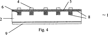
図4は、断面図で選択的エミッタ/コレクタのより有効な解決策を示すが、選択的エミッタ/コレクタは、表面側の金属コンタクト3の下に高いドーパント表面濃度と、隣接領域5にキャリアの捕獲に最適な狭いドーピング形状と、を有して、より深いエミッタ/コレクタドーピング形状領域6を有している。しかし、選択的エミッタ/コレクタ構造は、例えばDE42 17 428に記載するように一層複雑な製造方法を必要とし、ここには、薄いエミッタ層が、基板表面側の表面全部に渡って拡散され、その後に被覆保護/酸化物層が形成される。次いで、酸化物層には、エミッタコンタクト領域の深い拡散工程のために、レーザビームと、マスクとして利用される酸化物層と、を使用して、開口部が形成される。そして、金属コンタクト3、4は、レーザで開口された溝の中に形成される。
EP−A−680099から、p型シリコン基板の完全な上面に形成された第1のn型層と、基板の裏面上に形成されて基板よりも不純物濃度の高いp型層と、第1のn型層とp型層とを接続するように少なくとも基板の側面上に形成された第2のn型層とを含む太陽電池が知られている。第2のn型層は、p型層と接触する領域の周囲では、n型層よりも不純物の濃度が低く、シリコン基板の上面に塗着された液体ドーパントの外方拡散法により形成することができる。
USP4,152,824は、浅い/深い接合の装置構造を含む太陽電池の製造方法を開示している。太陽電池は、表側のエネルギー受容面にグリッド状のコンタクトを有し、各コンタクトの各位置が深い接合領域と一致、即ち整合していて、浅い接合領域は放射状に配置されている。複合的な接合とコンタクトとは、従来の技術、特に、パターン化されてドープされた酸化物皮膜の拡散源としての使用法、を利用する方法によって形成され、高ドープ領域を形成するのに、気相拡散が暴露された基板の上に行われる。
GB1,470,241は、コレクタグリッド又は電極直下に形成された第1のn+領域と、そのn+領域より少なく薄く且つn+領域のメッシュの網目に形成された第2のN-領域と、から成っている。これらのn+領域とN-領域とは選択的2重拡散法とマスキング法及び又は写真法の公知の方法により形成されている。
スクリーン印刷などの低コストの金属被覆法を利用する選択的エミッタ/コレクタの公知の製造方法は、第2の拡散工程及び/又はマスキング工程及び/又はエッチング工程が必要であり、金属被覆パターン3が半導体装置の表面の高ドープ領域6と正確に一致することが必要となる。
光電池の一般的な製造方法は、R. J. Overstraeten and R. P. Mertensの「光起電力の物理と技術と利用」(Physics, technology and use of Photovoltaics″),Adam Higler Ltd., 1896に記載され、ここに参照している。
発明の開示
本発明の製造方法は、請求の範囲1から13に規定されている。本発明の半導体装置は、請求の範囲14から24に規定されている。
本発明は、基本的には、半導体基板上に2つの異なる選択的な拡散領域を、異なるドーピングレベルで、形成するのに適用する。選択的なエミッタ又はコレクタ構造の有利な設計は、均質なエミッタ/コレクタ構造に比較して、余分な処理工程や処理の複雑さなしに、実現されることである。最も好ましい処理手順は、固体系のドーパントペーストをスクリーン印刷して第1の高温処理工程により拡散領域を形成すること、及び、金属ペーストをスクリーン印刷して第2の高温熱処理により金属被覆をすることを利用する。
本発明により、例えば、光電池のための選択的エミッタ又はコレクタ処理は、通常の均質エミッタ/コレクタ処理と同じ数の処理があるか、又は、従来の選択的均質エミッタ/コレクタ処理より少ない工程でよい。本発明の方法は、光電池用の単純で経済的な製造方法を提供し、公知の均質なエミッタ/コレクタ構造を越える優れた効果がある。ドーパント源材料は、均質エミッタ/コレクタ処理ほどは必要でなく、それで、製造コストを低減して電池の最終性能を改善するものである。
本発明は、公知のエミッタ又はコレクタ形成処理手順を単純化するものである。本発明のよる選択的エミッタ又はコレクタの構造は、ただ1回の拡散工程で形成される。選択的エミッタ又はコレクタの形成のためには、余分なマスキング工程及び/又はエッチング工程も必要でない。
【図面の簡単な説明】
図1は、公知の半導体装置の模式的な上面図を示す。
図2は、均質エミッタ/コレクタ構造を備えた公知の太陽電池の模式的断面図を示す。
図3は、選択的エミッタ/コレクタ構造を備えた公知の太陽電池の模式的断面図を示す。
図4は、選択的エミッタ/コレクタ構造を備えたさらに公知の太陽電池の模式的断面図を示す。
図5から図10までは、本発明の実施形態に係る半導体装置の製造における模式的な工程を示す。
図11は、本発明による直接間接拡散法を概念的に示す。
図12は、本発明の半導体装置の横方向広がり抵抗のプロット図を示す。
図13から図16は、本発明の別の実施形態の半導体装置の模式的な製造工程を示す。
実施形態の説明
以下には、本発明が、ある特別の実施形態を参照して、また図面を参照しながら説明するが、本発明は、請求の範囲以外には、これらには、制限されない。図面では、ある寸法、例えば、層の厚みは、明確にするために、誇張されている。特に、本発明は、太陽電池と呼ばれる光起電力装置について説明するが、本発明はこれに制限されず、一般的な半導体装置への適用を見出すことができる。さらに、本発明は、p型基板に、領域をn++型とn+型とを区別して形成するように主に説明している。本発明は、これに制限されない。本発明の方法は、n型基板に区別されたp型領域を形成すること、又は、アンドープ基板やn型基板にn++型とn+型の領域を形成すること、或いは、アンドープ基板又はp型基板にp++又はp+型の領域を形成するのに適用することができる。さらに、本発明は、単面太陽電池に関して説明するが、両面太陽電池にも等しく適用することができる。
1回の高温処理だけで、エッチングもマスキングも利用しないで、異なったドープ領域のある例えばエミッタ又はコレクタを形成するために本発明による単純な処理を利用することは、太陽電池には限られない。この技術は、ドープ領域と金属コンタクトと拡散形状との横方向の寸法が同様の許容度がある限りにおいて、他のマイクロエレクトロニクス製造法に利用することが出来る。あらゆる種類の光検出器、マイクロ技術センサ、熱電変換半導体装置が、サイリスタなどの全ての種類の半導体装置と同様に、本発明による方法を利用することができ、製造コストの低減が達成される。
図5から図10までは、本発明による選択的エミッタ又はコレクタ製造方法を、太陽電池1に適用するように、模式的に示す。本発明の低コスト製造方法では、処理は、切断のままの半導体基板2から始める。基板2は単結晶、多結晶、又は非晶質のシリコンでもよい。基板の品質は、トランジスタ装置ほどは要求されず、例えば、Martin Green著「太陽電池(″solar cells″)1992, New south Wales大学に記載のような太陽電池級でよい。基板2の大きさには制限がなく、大きさは、商業的に入手可能な材料に依存している。現在では、厚み200〜400ミクロンで10cm×10cmシリコン基板が使用できるが、本発明はこれに限られない。本発明による基板2は、好ましくはシリコンであるが、これに限られない。基板2は、ドーピングレベルに選択的な差がある互いに隣接した拡散ドープ領域を必要とするGaAsや、別の同様の半導体基板2でもよい。
始めに、半導体基板2は、化学的に洗浄され、その基板は、その後、切断による損傷を除去するために、脱イオン水(DI水)中に重量で40%のNaOH溶液で80℃2〜4分間、表面がエッチングされる。基板は、8 MOhmcmまで、DI水ですすぐ。任意的であるが、片方又は両方の主面には、Willeke and Fathにより「多結晶シリコン太陽電池のテクスチュア処理法」(Texturization methods for multicrystaline silicin solar cells″),Proce. 13th European Photovoltaic Solar Energy Conf. and Exhibition, France, 23-27 Oct. 1995に記載の如く、テクスチュア、例えば、ピラミッド構造が、機械的又は化学的に備えられてもよい。例えば、この目的のエッチ液は、DI水中に1.3wt%NaOHと容積で5%イソプロピルアルコールの溶液で90℃で10分を含む。エッチング後には、基板2は、前と同様に、化学的に洗浄し、DI水中で、すすぐ。図中にはテクスチュア組織は、明瞭さの理由から省かれている。
本発明では、深い濃厚ドープ拡散領域12は、表面側の表面金属コンタクト領域20(図8、9)の下に形成され、浅くて弱くドープされたエミッタ又はコレクタ領域15が、他の場所に形成される(図6)。図5に模式的に示すように、適当なドーパントを含みペースト状の固体系のドーパント源11が基板2の少なくとも片方の主面上に、線又は面の形をとるように、規定されたパターンで、選択的に適用される。ペースト11は、基板表面のこれらの領域に選択的に塗着され、ここには、深い拡散領域12が、後の工程で形成されるはずである。いろいろな方法がドーパントペースト11を基板2に選択的に適用するのに利用できる。ドーパントペースト11の適用は、非常に明瞭で再現可能な方法で実施するのが好ましい。好ましい方法は、スクリーン印刷、オフセット、グラビア、インクジェット印刷、ペースト書き(past writing)等の良好な繰返し性能を持つものである。ペースト11は、大容量生産法で良好な再現性を保持するためには、スクリーン印刷法のような厚膜技術によって基板上に印刷するのが好ましい。表面側の金属被覆パターン20(図8と図9)が、後に基板2上に、先にドーパントペースト11が適用されたその深い領域12に整合させて、適用されなければならないので、ドーパントペースト11と表面の金属ペースト18との両方に適用するのに同じ方法を利用することができるのは利点である。スクリーン印刷の良好な再現性は、金属ペースト18の適用により、ペースト11を適用するのに使用したのと同じ方法を用いて且つ同じ種類のスクリーンを用いて、表側の表面金属被覆パターン20を形成することを可能にする。DEKモデル1760RSスクリーン印刷機がペースト11に利用できる。
P、B又はAs等を含むペースト11が、伝導タイプや基板2の化学的性質に依存するが、使用することができる。基板2がシリコンで、p型の伝導性を有する場合には、ペーストは、EP−0 108 065に記載したように、或いはベルギーのSoltech NVから入手可能なペーストP101のように、リン含有ペースト11がよい。それに代えて、基板2が、シリコンで、n型伝導性を有する場合には、ペースト11はホウ素又はアルミニウムを含むんでもよい。本発明の好ましい低コスト太陽電池製造方法は、P型結晶Si基板とドーパント源としてリンとを使用して、表面にn型エミッター12、15を形成するものである。
ペースト11は、適当な方法、例えば、スクリーン印刷によって正確に塗着できるように、しかし、基板2上を著しく流れたり広がったりしないようにペースト11の粘度を選択すべきである。ペースト11は、チクソトロピー性であるのが好ましい。ドーパントペースト11の粘度は、後に適用される表側の表面金属コンタクト20の幅よりも塗着ドーパントペースト11の線又は面を著しく広くするような乾燥の前又はその途中で、或いは熱処理工程の中での横方向への流れを防止できるほど、高いことが好ましい。しかし、ペースト11の線や面が、その後に、金属コンタクト20により被覆されるであろうと意図した線や面を越えて横方向に少し広がることは、金属コンタクト20との接合部8の分路を避けるために好ましい。その後の金属コンタクト20の適用が、ある精度の範囲内でなされ、ペースト線又は面11がその後の金属コンタクトの線又は面20よりわずかに大きければ、好都合であり、深いドープ領域を有する金属ペースト線又は面18の調節が、繰り返し且つ正確に実施することができる。
好ましくは、ペースト11は、塗着後直ちに乾燥される。パターン化した基板2は、可能な限り速やかに、乾燥炉に装入され、粘性のあるペースト11が、150〜350℃の範囲、好ましくは150〜200℃の間で、約1〜10分で乾燥され、基板2上の所定位置に固定される。乾燥について、テンプレス(Tempress)コンベアベルト乾燥機、DEK赤外線ベルト乾燥機等が利用できる。ペーストの乾燥後は、基板2には、2段階熱処理の工程を施す。乾燥ペーストを有する基板2は、オランダのゲムコ社製のテンプレス/リンドバーグ(Tempress/Lindberg)コンベアベルト拡散炉など、拡散炉に直接、装入される。
第1段階では、温度は、毎分約100〜150℃で約600℃まで上昇され、ドーパントペーストの残留有機物成分が、空気又は酸素雰囲気で焼尽される。
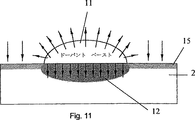
第2段階では、ドーパントが、高温中で、ペースト11から直接に基板中に導入される。この2番目の熱処理は、好ましくは、不活性雰囲気中で実施される。この高温工程で、深いドープ領域が、図6に示すように、形成され、ドーパントペースト11からのドーパントが、ペースト面又は線面直下の基板中に直接拡散される。同時に、浅い領域15が、ドーパント11から周囲雰囲気中にそして、そこから基板2上の露出面域への間接拡散により、形成される。
好ましくは、パターン化した基板2は、水平移動可能なベルト上に置かれて、連続炉、例えば、上記のテンプレス/リンドバーグコンベアベルト拡散炉の中に入り、窒素などの不活性ガス雰囲気中に保持される。温度は、150℃/minの温度勾配を維持して、800ないし1100℃に、好ましくは、900ないし950℃に、上げられる。基板2は、好ましくは、この温度で、約10から60分保持される。ペースト11が基板2に接触している場所では、基板2内にペースト11からのドーパントの内方拡散だけでなく、ドーパント原子が、周囲雰囲気中から基板2内に間接的に再度入る外方拡散もある。間接拡散は、ドーパントペースト11が適用された領域近傍の場所に、第2の拡散領域15を形成する。図11に模式的に示すように、ドーパント原子は、ドーパントペーストからあらゆる方向に拡散し始める。こうして、下側半導体基板2は、基板表面の他の領域に比べて、ペースト12が直接接触する領域12では、ドーパント原子の相対的に強い内方拡散を受ける。ドーパントは、ドーパントペースト11が適用されなかった場所では、周辺雰囲気から基板2内に拡散する。この間接ドーピングは、ペースト11が適用された基板2直下の第1の拡散領域12よりも低い濃度を有する第2の拡散層15を基板2内に形成する。高温工程で、基板2周囲の雰囲気中のドーパント原子の低い濃度もまた、第1の拡散領域12に比較して、第2の浅い拡散層15に導かれる。雰囲気ガス中のドーパント原子の濃度は、ペースト11それ自体の中よりも低くあってもよく、その結果拡散速度は、大変低い。その結果は、ドーパント源が基板2と接触する所では、比較的深いドープ領域になり、基板−ガス界面では、弱くて浅いドープ領域となる。2つの拡散領域の違いは、ドーパントペースト組成、雰囲気、拡散時間又は拡散温度を変えることにより、感度よく制御できる。第1の拡散領域が、接合部8をシャントさせずに、良好なオーミック前部表面金属コンタクト20の形成を可能にするのに十分深くて、しかも浅い第2の拡散層15を形成するために条件を最適化することができる。また、閉じた管状炉を使用して、例えば、POCl3、BBr3等のようなガス状ドーパント雰囲気を使用して拡散連続処理を実施することも可能である。ガス状ドーパントガスからの直接拡散と第2拡散領域15へのドーパントペースト11からの間接拡散との相対量を調整することにより、第1と第2の拡散領域12、15の拡散プロフィルを選択的に且つ独立的に制御することができる。さらに、一種以上のペースト11を使用して、熱処理により、基板2内に異なる領域を選択的に形成することもできる。異なるペースト11は、ドーパント原子の濃度が異なってもよく、異なった型のドーパントを含んでもよい。さらに、あるペースト11は、ドーパント原子を含ませずに、基板の下層の間接ドーピングを妨げるためマスクとして使用してもよい。
半導体装置1が光電池であって、エミッタまたはコレクタ領域の一部を構成する深い第1の拡散領域12の深さ又はドーパント濃度の変化は、電池性能に大きくは影響しないが、浅い第2の拡散領域15は、電池特性に顕著な影響を与える。第2の拡散領域15は、通常は、深い領域12よりも表面ドーパント濃度が非常に低く、深さが小さい。第2の拡散領域15のためのドーピング条件は、キャリヤの捕集のために最適化することができる。キャリアの捕獲は、ドーパント濃度と深さに敏感である。他方、第1の拡散領域12内での拡散は、拡散ペースト12が塗着され、金属被覆パターン18が処理工程で後に印刷されるところでは、十分に深くして十分に高い表面ドーパント濃度にしなければならず、それにより、接合部8をシャントさせずに、エミッタ又はコレクタ領域12で良好なオーミックコンタクト20を形成することができる。
本発明の方法では、単一のドーピング工程だけで、深いのと浅いのとに区分したドープ領域12、15が作られる。表面ドーパント濃度は、深い方のドープ領域では、通常は、例えば、1020リン原子/cm3以上の範囲内にあり、浅い方のドーパント領域15では、5×1018から1020、通常は、1×1019から5×1019リン原子/cm3の範囲とすることができる。接合部深さは、深い方の拡散領域12については、好ましくは、少なくとも0.3ミクロンであり、より好ましくは、少なくとも0.5ミクロン、典型的には、0.6ミクロンであり、浅い領域15については、0.3ミクロンまで、典型的には、0.2ミクロンである。図12は、J. R. Ehrstein, D. C. Gupta, and P. H. Langer; 「広がり抵抗測定−概要」Emerging Semiconductor Technology ASTM STP 960, Am. Soc. for Test. and Mat. 1986の記事に依拠して実施され、本発明の方法により製造された太陽電池のための選択的エミッタ又はコレクタ構造の横方向広がり抵抗分布を示す。ペーストライン11は、100ミクロンの幅で、互いに約3mmの距離で、隔設されている。選択的エミッタ又はコレクタ構造は、金属被覆20が適用されるべき場所では、抵抗が低くて深くて強い拡散領域12を有し、光が吸収されてキャリアが発生するエミッタ又はコレクタ領域15では、浅くて弱い拡散領域15を有している。図12から判るように、ペーストは、それ自体の幅の大きさについて狭い距離にわたって低抵抗領域12になる。抵抗は、浅い領域に向けて約1mmの距離で単調に低下する。深い領域12と浅い領域15での抵抗比は、約5であり、太陽電池では、約10以上である。これは、これらの領域のドーパント原子濃度の同様の変化によって生じる。完成した装置では、深い拡散領域12と浅い拡散領域15とが、周期的に繰り返えされて、遷移領域では急峻な勾配を示し、ドーパント原子の表面濃度が、大まかに、1桁の強度の違いを生じている。ドーパント濃度が高いほど、電気抵抗は低い。ドーパント濃度の単調増加と、弱いドープ領域15から金属コンタクト20が最終の太陽電池で配置される深い拡散領域12への合成の電気抵抗は、優れたキャリア捕獲特性を提供する。金属コンタクト20が最終の太陽電池に配置される領域に向けてドーパント原子の表面濃度の増加勾配は、これらの捕獲コンタクト20へのキャリア輸送を容易にする。本発明によれば、ドーパント原子濃度の単調増加は、浅い領域15と深い領域12との間の基板2の表面領域で、浅い領域でのドーパント密度と深い領域でのドーパント密度の間に少なくとも5倍で、通常は、1オーダ以上の強度の差で、得られる。本発明の処理手順で太陽電池は、何らの処理工程を加えることなく、均質エミッタ又はコレクタ処理により製造した太陽電池と比較して、>1%の高い絶対効率で、製造することができる。
拡散処理後には、シリコン基板表面に残る拡散ガラスが、DI水中25%〜50%HFの化学エッチング溶液中で除去され、基板2は洗浄され、その後すすがれる。本発明は、拡散ガラスを付随的に除かずに、処理を酸化/皮膜形成工程に続けることを含む。
図7に模式的に示すように、拡散処理の後に付随的な酸化工程が続き、ここでは、基板を、通常は、石英ボートに、約1〜20分間800〜950℃の範囲の温度で、O2雰囲気に曝すことにより、SiO2層16a、16bが基板表面上に形成される。このSiO2層16a、16bは、太陽電池性能を低下させ得る基板2の表面のエミッタ/コレクタ領域15中の欠陥を被覆保護するのに役立つ。酸化物層を利用する被覆保護は、キャリアの損失を低下させる表面の再結合速度を低下させ、ここに、効率を改善する。任意であるが、酸化物のような被覆保護層16a、16bを適用するだけでなく、反射防止層(ARC)17も適用できる。ARC層17は、化学的生成法(CVD、例えば、TiO2層)又はプラズマ強化CVD(PECVD、例えば、窒化シリコン層)又は同様な方法が利用できる。ARC層の適用は、半導体基板の表面と内部の優れた被覆保護化となる。
最後に、金属被覆手順は、通常は、2つ又は3つのコンタクト印刷工程を含み、表面コンタクト20と、異なる材料の種類の数によって1つ又は2つの裏面コンタクトパターン21が使用される。図8に示したように、金属ペースト18が、基板の表面側に、多量ドープされた領域12に整合するようにして、選択的に適用される。さらに金属ペースト19が、選択的にまたは非選択的のいずれかで基板裏側に適用される。スクリーン印刷とその後の乾燥がこれらコンタクトを適用するのに最も好ましい方法であるが、上記の他の厚膜技術、蒸着法又は水溶液からのメッキ法も、その代わりに使用できる。各印刷工程の後に、乾燥工程が、250℃程度の温度で、例えば赤外線ヒータによって、なされる。図9に示したように、金属ペースト18、19は、次いで、650から900℃の温度範囲で、通常30から200秒、焼結されて、基板2の裏面に良好なオーミックコンタクト21と同様に、接合部8をシャントすることなく、良好なオーミックコンタクト20を基板の表面側に形成する。コンタクト20と21は、ARC又は酸化物層16b、17を通じて形成される。最高温度と温度プロフィル(温度対時間)は、非常に重要であり、金属被覆ペーストと処理手順毎に適合されなければならない。通常は、金属ペースト18、19でスクリーン印刷された表面コンタクトと裏面コンタクトは、別個に乾燥されたあと、高温段階で同時に焼結される。また、付随的に、裏面フィールド(BSF)層22は、図9に模式的に示すように基板2の裏側に、同時に形成される。BSF22の形成のために、高い温度とアルミニウムペーストが裏面金属コンタクト21の形成のために使用されれば、好ましい。
図10に概略的に示したように、付随して、反射防止膜(ARC)層23が、図18に関連して述べた金属皮膜形成の前に適用されるARC層17よりもむしろ、金属皮膜形成の後に適用することができる。典型的なARC層は、TiO2、Si3N4、Ta2O5又は同様の材料を含み、いろいろな方法で適用することができる。
800℃程度の金属コンタクト焼結温度が、接合部8のシャントなしにコンタクト形成するために利用される。金属コンタクトのためにアルミニウムを利用する場合は、そのような高温での焼結は、例えば、AlゲッタリングとBSF形成に付随的な利点がある。
金属ペースト及び又はドーピングペーストを適用するためのスクリーン印刷などの厚膜技術は、優れた再現性を示す。基板2は、CCDカメラ制御位置づけシステムにより、スクリーン印刷機よってそのたびに同じ場所にスクリーン下で負荷を受ける。もし、酸化物及び/又はARC層16a、16b、17、23を、顕微鏡観察下で、わずかに広い第1の拡散領域12と違った色を利用して適用されれば、金属被覆パターンと拡散パターンの配列を制御することができる。ARC層17、23を塗着すると、基板2は、基板が高いドーパント表面濃度を有するこれらの場所では、違った色を示す。これは、ドーパント表面濃度が高い場所では、より低いドーパントレベルの領域15上の酸化物層16aに比べると、下部酸化物層16bが厚く成長するからである。反射防止膜(ARC)層17又は23が適用される限り、下側パターンは見ることができる。この理由は、高いドーパント表面濃度を有する場所は酸化が速く、その結果酸化物層16が厚くなるからである。ARC層17又は23が適用された後は、酸化物の厚みの違いが、層16a+17又は23に比較して、層16b+17又は23の光学的に厚みの違い、従って、色の違いとして目に見えるようになる。
本発明に従って単純な処理手順で、改良した性能(捕獲効率)を有する選択的エミッタ/コレクタ太陽電池を形成することができ、処理を複雑化せずに製造コストを増加させない。その結果が、太陽電池の費用効果の高い製造である。スクリーン印刷拡散が既に利用されているので、余分な或いは複雑な処理装置は、必要でない。選択性エミッタを使用するので、同時に、処理許容度が高められる。例えば、金属被覆焼結工程については、色々な処理パラメータの変化は、均質なエミッタ又はコレクタ処理ほどは、厳密ではない。この結果、高い処理量があり、費用効果を一層高める。
図13から図16は、本発明の実施例に従って、半導体装置30の製造工程を概念的に示すが、1つの実施例は、図5から10を参照して詳細に、既に説明したので、次の実施例の説明は、詳細にはしない。被覆層の形成、洗浄工程、ドーピング工程以外の他の処理の詳細は、述べない。次の実施例の処理は、光装置の成形に適当である。
図13に示すように、第1のドープペーストパターン31は、シリコン基板であって、アンドープ半導体、p型又はn型半導体である半導体基板上に選択的に適用される。ペースト31は、前に述べた厚膜法のいずれかによって、適用することができる。ペーストパターンは、乾燥される。第1のドーパントペースト31は、第1又は第2のタイプの伝導性があってもよい。第1のペーストパターン31は、付随的に、別の材料の層、例えば、さらに別のペースト21により保護される。ペースト32は、ペースト31に比較して、違った濃度又はタイプを持つことができ、又は、ドーピングされなくてもよい。ペースト32は、基板2の主面上に適用されてもよい。ペースト32は、次いで、乾燥される。
図14に示すように、付随的に、第3のペーストパターン33が、基板2の他方の主面上にも適用される。ペーストパターンは、そこで乾燥される、ペースト33は、第1又は第2の伝導タイプであってもよい。ペーストパターン33と基板2の表面の他の選択された部分が、ペーストであるドープされない材料を選択的に適用することによって保護されるのがよい。ペースト34は、上記の厚膜法のどれかで適用される。
図15に示すように、別のドープペーストパターン35が、基板2の主面に適用される。ペースト35は、いずれかの伝導タイプのドーパントを含んでもよい。ペースト35は、上記の厚膜法のどれかで適用できる。次いで、ペーストパターン35は、乾燥される。
次いで、パターン形成した基板2は、炉内に配置され、ドーパント原子を含むペースト31、33、35からのドーパントは、それぞれドープ層37、39、41を形成するように基板内に導入される。同時に、保護されないペーストからのドーパント原子は、基板2の領域42内に間接的に拡散して、浅くて弱いドープ領域42を形成する。最後には、金属ペーストが領域37、39、付随的に41上に合致するように適用され、高温で焼結されて、それぞれ金属コンタクト36、38、付随的に40を形成する。
さらに別の実施例の処理においては、基板2は、p型シリコンで、ペースト31、35、付随的に32が、リン含有ペーストであってもよく、ペースト33がホウ素又はアルミニウム含有ペーストで、ペースト34がドープされないものでよい。層32がドーパントを含むとき、高温導入工程により、半導体基板の第1の主面上のドープ領域37の間にドープ領域43(図16中に破線で示す)になる。その代わりとして、図13と図14中、保護ペースト32は省略されてもよく、それにより、導入工程の後には、高濃度ドープ領域37の間に間接拡散による弱いドープ領域(図16中破線で示す)になる。別の変形として、図14中で、層32と31は省略されて、第1の主面全部が間接拡散層43(図16中破線で示す)になり、導入工程後は、浮揚接合部になる。
本発明の更なる実施例により単一拡散工程で作った装置は、太陽電池であってもよく、表の面には選択性のエミッタと、裏面には、浮揚接合部を有している。そのような光電池装置は、従来の裏面全面に金属被覆を有する単一面電池よりも、電池性能が高いことを示す。更なる実施例の方法によって作った装置は、両面型の太陽電池として付加的に利用することができる。
実施例による処理は、改良した効率と、理想的なエミッタ/コレクタ構造から生じた短絡電流と、より理想的な裏面コンタクトを持った太陽電池を製造するという利点がある。さらに実施例による裏面コンタクトに基板2の裏面主面に金属被覆を有せず、より良好な裏面反射や、両面電池の設計に使用できる。
本発明の好ましい実施例を上で述べたが、多くの変更や修正は、本発明の範囲と精神から逸脱することなく、この技術分野の専門家により容易になされることは理解できるはずである。Field of Invention
The present invention relates to a semiconductor device and a method for manufacturing the same, and more particularly, to a photovoltaic cell having two or more selective diffusion regions formed in a single diffusion step.
Background art
Many semiconductor devices have different doped regions with the same conductivity type (p or n) to achieve high device performance. Implementation of these different doped regions involves additional processing steps and increases manufacturing costs. A typical semiconductor device 1 is shown in the top view of FIG. 1, which is a photovoltaic cell, sometimes called a solar cell. The
Solar cells generally suffer losses in the emitter region. For optimum performance, the doping level in the emitter region is at a low level for light capture and conversion, whereas
For a solar cell as schematically shown in the cross-sectional view of FIG. 2, the homogeneous emitter / collector structure includes a
Normal homogeneous emitter / collector region processing procedures include structural chemical preparation of the wafer surface, diffusion steps (in-diffusion of dopants from the surface), additional oxide overcoat steps, and optional Additional anti-reflective coating processes that can also be provided for protective coatings (eg TiO 2 , Si Three N Four ) And a metal coating step (preferably screen printing).
An improvement of
FIG. 4 shows a more effective selective emitter / collector solution in a cross-sectional view, where the selective emitter / collector has a higher dopant surface concentration under the
From EP-A-68099, a first n-type layer formed on the complete upper surface of a p-type silicon substrate, a p-type layer formed on the back surface of the substrate and having a higher impurity concentration than the substrate, A solar cell including at least a second n-type layer formed on a side surface of a substrate so as to connect the n-type layer and the p-type layer is known. The second n-type layer has an impurity concentration lower than that of the n-type layer around the region in contact with the p-type layer, and is formed by the outward diffusion method of the liquid dopant applied to the upper surface of the silicon substrate. Can do.
USP 4,152,824 discloses a method for manufacturing a solar cell including a shallow / deep junction device structure. The solar cell has a grid-like contact on the front-side energy receiving surface, and each position of each contact coincides with, or is aligned with, a deep junction region, and the shallow junction region is radially arranged. Composite junctions and contacts are formed using conventional techniques, particularly the use of patterned and doped oxide films as diffusion sources, to form highly doped regions. Vapor phase diffusion is performed on the exposed substrate.
GB1, 470, 241 are the first n formed directly under the collector grid or electrode. + Region and its n + Less than area and n + A second N formed in the mesh of the region - And consists of an area. These n + Region and N - The region is formed by a known method such as a selective double diffusion method and a masking method and / or a photographic method.
A known method of manufacturing a selective emitter / collector utilizing a low-cost metal coating method such as screen printing requires a second diffusion process and / or a masking process and / or an etching process. It is necessary to exactly match the highly
The general method of manufacturing photovoltaic cells is described in RJ Overstraeten and RP Mertens, "Physics, technology and use of Photovoltaics", Adam Higler Ltd., 1896, see here. is doing.
Disclosure of the invention
The production method of the present invention is defined in claims 1 to 13. The semiconductor device of the present invention is defined in claims 14 to 24.
The present invention is basically applied to forming two different selective diffusion regions on a semiconductor substrate with different doping levels. An advantageous design of the selective emitter or collector structure is that it can be realized without extra processing steps and processing complexity compared to a homogeneous emitter / collector structure. The most preferred processing procedure is to screen-print a solid dopant paste to form a diffusion region by a first high-temperature treatment step, and to screen-print a metal paste to form a metal coating by a second high-temperature heat treatment. Is used.
In accordance with the present invention, for example, selective emitter or collector processing for photovoltaic cells may have the same number of processes as conventional homogeneous emitter / collector processes, or fewer steps than conventional selective homogeneous emitter / collector processes. . The method of the present invention provides a simple and economical manufacturing method for photovoltaic cells, and has superior advantages over known homogeneous emitter / collector structures. The dopant source material is not as necessary as a homogeneous emitter / collector process, so it reduces manufacturing costs and improves the final performance of the cell.
The present invention simplifies known emitter or collector formation processing procedures. The selective emitter or collector structure according to the present invention is formed in a single diffusion step. No extra masking and / or etching steps are required for selective emitter or collector formation.
[Brief description of the drawings]
FIG. 1 is a schematic top view of a known semiconductor device.
FIG. 2 shows a schematic cross-sectional view of a known solar cell with a homogeneous emitter / collector structure.
FIG. 3 shows a schematic cross-sectional view of a known solar cell with a selective emitter / collector structure.
FIG. 4 shows a schematic cross-sectional view of a further known solar cell with a selective emitter / collector structure.
5 to 10 show schematic steps in the manufacture of the semiconductor device according to the embodiment of the present invention.
FIG. 11 conceptually illustrates the direct and indirect diffusion method according to the present invention.
FIG. 12 shows a plot of the lateral spreading resistance of the semiconductor device of the present invention.
13 to 16 show schematic manufacturing steps of a semiconductor device according to another embodiment of the present invention.
Description of embodiment
In the following, the present invention will be described with reference to certain specific embodiments and with reference to the drawings, but the present invention is not limited thereto except the scope of the claims. In the drawings, certain dimensions, such as layer thickness, are exaggerated for clarity. In particular, the present invention describes a photovoltaic device called a solar cell, but the present invention is not limited to this and can find application to a general semiconductor device. Furthermore, the present invention provides a p-type substrate with a region n. ++ Type and n + Mainly explained so as to distinguish from the mold. The present invention is not limited to this. The method of the present invention forms a distinct p-type region on an n-type substrate, or n on an undoped substrate or n-type substrate. ++ Type and n + Forming a region of a mold, or p on an undoped substrate or a p-type substrate ++ Or p + It can be applied to form mold regions. Furthermore, although the present invention will be described with respect to single-sided solar cells, it is equally applicable to double-sided solar cells.
Using a simple process according to the present invention to form, for example, emitters or collectors with different doped regions, with only one high temperature process, without etching or masking, is not limited to solar cells. . This technique can be used in other microelectronic manufacturing methods as long as the lateral dimensions of the doped region, metal contact, and diffusion shape have similar tolerances. All types of photodetectors, micro-technical sensors, thermoelectric conversion semiconductor devices, like all types of semiconductor devices such as thyristors, can utilize the method according to the present invention, achieving a reduction in manufacturing costs.
FIGS. 5 to 10 schematically show the selective emitter or collector manufacturing method according to the present invention as applied to the solar cell 1. In the low-cost manufacturing method of the present invention, the processing starts with the
First, the
In the present invention, the deep heavily doped
A
The viscosity of the
Preferably, the
In the first stage, the temperature is raised to about 600 ° C. at about 100-150 ° C. per minute and the residual organic components of the dopant paste are burned out in air or oxygen atmosphere.
In the second stage, the dopant is introduced directly from the
Preferably, the patterned
The semiconductor device 1 is a photovoltaic cell, and a change in the depth or dopant concentration of the deep
In the method of the present invention,
After the diffusion treatment, the diffusion glass remaining on the silicon substrate surface is removed in a chemical etching solution of 25% to 50% HF in DI water, and the
As schematically shown in FIG. 7, the diffusion treatment is followed by an additional oxidation step, where the substrate is typically placed in a quartz boat at a temperature in the range of 800-950 ° C. for about 1-20 minutes. O 2 By exposing to the atmosphere, SiO 2 Layers 16a and 16b are formed on the substrate surface. This SiO 2 Layers 16a, 16b serve to cover and protect defects in the emitter /
Finally, the metallization procedure typically includes two or three contact printing steps, with one or two
Concomitantly, as shown schematically in FIG. 10, an anti-reflective coating (ARC)
A metal contact sintering temperature on the order of 800 ° C. is used for contact formation without shunting of the
Thick film technology such as screen printing for applying metal paste and / or doping paste exhibits excellent reproducibility. The
A simple emitter / collector solar cell with improved performance (capture efficiency) can be formed with a simple processing procedure in accordance with the present invention without complicating processing and increasing manufacturing costs. The result is cost-effective manufacturing of solar cells. Since screen printing diffusion is already utilized, no extra or complicated processing equipment is required. Since a selective emitter is used, the processing tolerance is increased at the same time. For example, for a metallized sintering process, changes in various process parameters are not as strict as homogeneous emitter or collector processes. This results in high throughput and further increases cost effectiveness.
FIGS. 13 to 16 conceptually show the manufacturing process of the semiconductor device 30 according to the embodiment of the present invention. Since one embodiment has already been described in detail with reference to FIGS. This embodiment will not be described in detail. Details of processes other than the formation of the coating layer, the cleaning process, and the doping process will not be described. The process of the following embodiment is suitable for forming an optical device.
As shown in FIG. 13, the first doped
As shown in FIG. 14, incidentally, the
As shown in FIG. 15, another
The patterned
In yet another embodiment of the process, the
A device made in a single diffusion process according to a further embodiment of the present invention may be a solar cell, with a selective emitter on the front side and a levitation junction on the back side. Such a photovoltaic cell device shows higher battery performance than a conventional single-sided battery having a metal coating on the entire back surface. The device made by the method of the further embodiment can additionally be used as a double-sided solar cell.
The process according to the embodiments has the advantage of producing solar cells with improved efficiency, short circuit currents resulting from an ideal emitter / collector structure, and a more ideal back contact. Furthermore, the back surface contact according to the embodiment does not have a metal coating on the back surface main surface of the
While the preferred embodiment of the present invention has been described above, it should be understood that many changes and modifications can be readily made by those skilled in the art without departing from the scope and spirit of the invention. .
Claims (13)
工程1)固体系ドーパント源のパターンを半導体基板上の第1の主面に選択的に適用する工程であり、第1の主面上に上記固体系ドーパントにより覆われる領域と、上記固体系ドーパントにより覆われない領域と、を形成する工程と、
工程2)半導体基板を取り巻く気相環境内における制御された熱処理過程により上記固体系ドーパント源から基板内にドーパント原子を拡散させる工程であり、固体系ドーパント源からのドーパントを直接に上記基板中に拡散させて、固体系ドーパント源のパターン直下の上記基板内に第1の拡散領域を形成し、それと同時に、上記固体系ドーパント源からのドーパントを気相環境を介して間接的に基板内に拡散させて、パターンで覆われていない基板上の領域の少なくともいくつかに第2の拡散領域を形成する工程と、
工程3)上記第2の拡散領域を実質的にエッチングすることなく、金属コンタクトパターンを上記第1の拡散領域に実質的に整合するように形成する工程と、を含み、
上記第1の拡散領域が、上記第2の拡散領域に比べて、深さが深く、且つドーパントの濃度が高いことを特徴とする光電池の製造方法。A method of manufacturing a photovoltaic cell including a slice-shaped semiconductor substrate, the manufacturing method comprising:
Step 1) A step of selectively applying a solid dopant source pattern to a first main surface on a semiconductor substrate, the region covered with the solid dopant on the first main surface, and the solid dopant Forming a region not covered by,
Step 2) A step of diffusing dopant atoms from the solid dopant source into the substrate by a controlled heat treatment process in a gas phase environment surrounding the semiconductor substrate, and the dopant from the solid dopant source is directly introduced into the substrate. A first diffusion region is formed in the substrate immediately below the pattern of the solid dopant source by diffusing, and at the same time, the dopant from the solid dopant source is indirectly diffused into the substrate through the gas phase environment. Forming a second diffusion region in at least some of the regions on the substrate not covered by the pattern;
Step 3) forming a metal contact pattern substantially aligned with the first diffusion region without substantially etching the second diffusion region;
The method for manufacturing a photovoltaic cell , wherein the first diffusion region is deeper than the second diffusion region and has a high dopant concentration.
Applications Claiming Priority (3)
| Application Number | Priority Date | Filing Date | Title |
|---|---|---|---|
| EP96120865A EP0851511A1 (en) | 1996-12-24 | 1996-12-24 | Semiconductor device with two selectively diffused regions |
| EP96120865.9 | 1996-12-24 | ||
| PCT/EP1997/007246 WO1998028798A1 (en) | 1996-12-24 | 1997-12-22 | Semiconductor device with selectively diffused regions |
Related Child Applications (1)
| Application Number | Title | Priority Date | Filing Date |
|---|---|---|---|
| JP2007139083A Division JP2007235174A (en) | 1996-12-24 | 2007-05-25 | Photovoltaic cell having selectively diffused region |
Publications (3)
| Publication Number | Publication Date |
|---|---|
| JP2002503390A JP2002503390A (en) | 2002-01-29 |
| JP2002503390A5 JP2002503390A5 (en) | 2005-09-08 |
| JP3999820B2 true JP3999820B2 (en) | 2007-10-31 |
Family
ID=8223558
Family Applications (2)
| Application Number | Title | Priority Date | Filing Date |
|---|---|---|---|
| JP52840198A Expired - Lifetime JP3999820B2 (en) | 1996-12-24 | 1997-12-22 | Method for manufacturing photovoltaic cell having selective diffusion region |
| JP2007139083A Pending JP2007235174A (en) | 1996-12-24 | 2007-05-25 | Photovoltaic cell having selectively diffused region |
Family Applications After (1)
| Application Number | Title | Priority Date | Filing Date |
|---|---|---|---|
| JP2007139083A Pending JP2007235174A (en) | 1996-12-24 | 2007-05-25 | Photovoltaic cell having selectively diffused region |
Country Status (10)
| Country | Link |
|---|---|
| EP (2) | EP0851511A1 (en) |
| JP (2) | JP3999820B2 (en) |
| CN (1) | CN1155104C (en) |
| AT (1) | ATE281698T1 (en) |
| AU (1) | AU741153B2 (en) |
| CA (1) | CA2276008C (en) |
| DE (1) | DE69731485T2 (en) |
| DK (1) | DK0960443T3 (en) |
| ES (1) | ES2232887T3 (en) |
| WO (1) | WO1998028798A1 (en) |
Families Citing this family (75)
| Publication number | Priority date | Publication date | Assignee | Title |
|---|---|---|---|---|
| JP2000138386A (en) * | 1998-11-04 | 2000-05-16 | Shin Etsu Chem Co Ltd | Manufacturing method of solar cell and solar cell manufactured by the method |
| EP1024523A1 (en) * | 1999-01-27 | 2000-08-02 | Imec (Interuniversity Microelectronics Center) VZW | Method for fabricating thin film semiconductor devices |
| NL1012961C2 (en) * | 1999-09-02 | 2001-03-05 | Stichting Energie | A method of manufacturing a semiconductor device. |
| KR100420030B1 (en) * | 2001-04-23 | 2004-02-25 | 삼성에스디아이 주식회사 | Method for manufacturing solar cell |
| GB0114896D0 (en) * | 2001-06-19 | 2001-08-08 | Bp Solar Ltd | Process for manufacturing a solar cell |
| EP1378947A1 (en) | 2002-07-01 | 2004-01-07 | Interuniversitair Microelektronica Centrum Vzw | Semiconductor etching paste and the use thereof for localised etching of semiconductor substrates |
| JP4121928B2 (en) | 2003-10-08 | 2008-07-23 | シャープ株式会社 | Manufacturing method of solar cell |
| JP4232597B2 (en) | 2003-10-10 | 2009-03-04 | 株式会社日立製作所 | Silicon solar cell and manufacturing method thereof |
| JP2006073617A (en) * | 2004-08-31 | 2006-03-16 | Sharp Corp | Solar cell and manufacturing method thereof |
| US7906722B2 (en) | 2005-04-19 | 2011-03-15 | Palo Alto Research Center Incorporated | Concentrating solar collector with solid optical element |
| US7799371B2 (en) | 2005-11-17 | 2010-09-21 | Palo Alto Research Center Incorporated | Extruding/dispensing multiple materials to form high-aspect ratio extruded structures |
| US7765949B2 (en) | 2005-11-17 | 2010-08-03 | Palo Alto Research Center Incorporated | Extrusion/dispensing systems and methods |
| US20070107773A1 (en) | 2005-11-17 | 2007-05-17 | Palo Alto Research Center Incorporated | Bifacial cell with extruded gridline metallization |
| KR20080091105A (en) | 2005-11-24 | 2008-10-09 | 뉴사우스 이노베이션즈 피티와이 리미티드 | High efficiency solar cell fabrication |
| CN101443893B (en) | 2005-12-21 | 2012-02-01 | 太阳能公司 | Back side contact solar cell structures and fabrication processes |
| US7851693B2 (en) | 2006-05-05 | 2010-12-14 | Palo Alto Research Center Incorporated | Passively cooled solar concentrating photovoltaic device |
| US8322025B2 (en) | 2006-11-01 | 2012-12-04 | Solarworld Innovations Gmbh | Apparatus for forming a plurality of high-aspect ratio gridline structures |
| US8226391B2 (en) | 2006-11-01 | 2012-07-24 | Solarworld Innovations Gmbh | Micro-extrusion printhead nozzle with tapered cross-section |
| US7780812B2 (en) | 2006-11-01 | 2010-08-24 | Palo Alto Research Center Incorporated | Extrusion head with planarized edge surface |
| US7922471B2 (en) | 2006-11-01 | 2011-04-12 | Palo Alto Research Center Incorporated | Extruded structure with equilibrium shape |
| US7638438B2 (en) | 2006-12-12 | 2009-12-29 | Palo Alto Research Center Incorporated | Solar cell fabrication using extrusion mask |
| US7928015B2 (en) * | 2006-12-12 | 2011-04-19 | Palo Alto Research Center Incorporated | Solar cell fabrication using extruded dopant-bearing materials |
| WO2008103293A1 (en) * | 2007-02-16 | 2008-08-28 | Nanogram Corporation | Solar cell structures, photovoltaic modules and corresponding processes |
| US7954449B2 (en) | 2007-05-08 | 2011-06-07 | Palo Alto Research Center Incorporated | Wiring-free, plumbing-free, cooled, vacuum chuck |
| ATE547812T1 (en) * | 2007-07-18 | 2012-03-15 | Imec | METHOD FOR PRODUCING AN EMITTER STRUCTURE AND RESULTING EMITTER STRUCTURES |
| DE102007035068A1 (en) * | 2007-07-26 | 2009-01-29 | Fraunhofer-Gesellschaft zur Förderung der angewandten Forschung e.V. | Method for manufacturing silicon solar cell with selective emitter, involves producing laminar emitter at emitter surface of solar cell substrate and applying corroding barrier on sub ranges of emitter surface |
| JP2010534927A (en) * | 2007-07-26 | 2010-11-11 | ウニベルジテーツ コンスタンツ | Silicon solar cell having emitter with back-etching and method of forming similar solar cell |
| JP5236914B2 (en) * | 2007-09-19 | 2013-07-17 | シャープ株式会社 | Manufacturing method of solar cell |
| US8222516B2 (en) * | 2008-02-20 | 2012-07-17 | Sunpower Corporation | Front contact solar cell with formed emitter |
| US8293568B2 (en) * | 2008-07-28 | 2012-10-23 | Day4 Energy Inc. | Crystalline silicon PV cell with selective emitter produced with low temperature precision etch back and passivation process |
| JP5344872B2 (en) * | 2008-08-27 | 2013-11-20 | 三菱電機株式会社 | Photovoltaic device |
| US7999175B2 (en) | 2008-09-09 | 2011-08-16 | Palo Alto Research Center Incorporated | Interdigitated back contact silicon solar cells with laser ablated grooves |
| US8117983B2 (en) | 2008-11-07 | 2012-02-21 | Solarworld Innovations Gmbh | Directional extruded bead control |
| US9150966B2 (en) | 2008-11-14 | 2015-10-06 | Palo Alto Research Center Incorporated | Solar cell metallization using inline electroless plating |
| US8080729B2 (en) | 2008-11-24 | 2011-12-20 | Palo Alto Research Center Incorporated | Melt planarization of solar cell bus bars |
| US8960120B2 (en) | 2008-12-09 | 2015-02-24 | Palo Alto Research Center Incorporated | Micro-extrusion printhead with nozzle valves |
| JP5029921B2 (en) * | 2009-01-19 | 2012-09-19 | シャープ株式会社 | Method for manufacturing solar battery cell |
| DE102009018653B4 (en) * | 2009-03-04 | 2015-12-03 | SolarWorld Industries Thüringen GmbH | Method for the production of semiconductor devices using doping techniques |
| DE102009041546A1 (en) | 2009-03-27 | 2010-10-14 | Bosch Solar Energy Ag | Process for the production of solar cells with selective emitter |
| KR101597825B1 (en) * | 2009-07-24 | 2016-02-25 | 엘지전자 주식회사 | Solar Cell Method for solar cell and Heat Treatment Apparatus for Thermal Diffusion |
| NL2003324C2 (en) * | 2009-07-31 | 2011-02-02 | Otb Solar Bv | Photovoltaic cell with a selective emitter and method for making the same. |
| KR101611456B1 (en) * | 2009-09-02 | 2016-04-11 | 엘지이노텍 주식회사 | Paste composition for manufacturing solar-cell electrode comprising phosphoric dispersant |
| US8735234B2 (en) * | 2010-02-18 | 2014-05-27 | Varian Semiconductor Equipment Associates, Inc. | Self-aligned ion implantation for IBC solar cells |
| WO2011110231A1 (en) * | 2010-03-12 | 2011-09-15 | Q-Cells Se | Method and in-line production system for the production of solar cells |
| KR101046219B1 (en) * | 2010-04-02 | 2011-07-04 | 엘지전자 주식회사 | Solar cell having a selective emitter |
| CN101866984B (en) * | 2010-05-18 | 2015-01-07 | 常州亿晶光电科技有限公司 | Method for selectively doping emitting stage on surface of crystalline silicon cell film |
| JP5734734B2 (en) * | 2010-05-18 | 2015-06-17 | ローム アンド ハース エレクトロニック マテリアルズ エルエルシーRohm and Haas Electronic Materials LLC | Method for forming current tracks on a semiconductor |
| CN101866971A (en) * | 2010-05-18 | 2010-10-20 | 常州亿晶光电科技有限公司 | Broken solar cells with selective emitting stage |
| DE102010024308A1 (en) * | 2010-06-18 | 2011-12-22 | Fraunhofer-Gesellschaft zur Förderung der angewandten Forschung e.V. | Method for producing a selective doping structure in a semiconductor substrate for producing a photovoltaic solar cell |
| JP5538103B2 (en) * | 2010-07-07 | 2014-07-02 | 三菱電機株式会社 | Method for manufacturing solar battery cell |
| US20110139231A1 (en) * | 2010-08-25 | 2011-06-16 | Daniel Meier | Back junction solar cell with selective front surface field |
| KR101733055B1 (en) * | 2010-09-06 | 2017-05-24 | 엘지전자 주식회사 | Solar cell module |
| CN102468364A (en) * | 2010-11-05 | 2012-05-23 | 无锡尚德太阳能电力有限公司 | Selective emitting electrode solar cell and manufacturing method thereof |
| WO2012067117A1 (en) * | 2010-11-17 | 2012-05-24 | 日立化成工業株式会社 | Method for producing solar cell |
| CN102110721A (en) * | 2010-12-17 | 2011-06-29 | 福建省上杭县九洲硅业有限公司 | Gradient type back surface field of polycrystalline silicon solar cell and preparation method thereof |
| CN102082210A (en) * | 2010-12-18 | 2011-06-01 | 广东爱康太阳能科技有限公司 | Method for manufacturing fine grid selective emitter crystalline silicon solar cell |
| KR101114198B1 (en) | 2010-12-31 | 2012-03-13 | 현대중공업 주식회사 | Localized emitter solar cell and method for manufacturing thereof |
| KR101198438B1 (en) | 2010-12-31 | 2012-11-06 | 현대중공업 주식회사 | Bifacial Photovoltaic Localized Emitter Solar Cell and Method for Manufacturing Thereof |
| DE102011002748A1 (en) | 2011-01-17 | 2012-07-19 | Robert Bosch Gmbh | Process for producing a silicon solar cell |
| US8962424B2 (en) | 2011-03-03 | 2015-02-24 | Palo Alto Research Center Incorporated | N-type silicon solar cell with contact/protection structures |
| KR101071546B1 (en) | 2011-04-26 | 2011-10-10 | 주식회사 톱텍 | Solar cell manufacturing method and the solar cell manufactured using the method |
| DE102011051040A1 (en) * | 2011-06-14 | 2012-12-20 | Solarworld Innovations Gmbh | Method for manufacturing e.g. quadratic solar cell, involves back etching portion of highly doped emitter region between portions of metallization structure by using metallization structure as etching mask |
| CN102306684B (en) * | 2011-09-19 | 2016-01-20 | 苏州旭环光伏科技有限公司 | Selective emitter of a kind of three grades of doped level and preparation method thereof |
| TWI424584B (en) * | 2011-11-30 | 2014-01-21 | Au Optronics Corp | Method of forming solar cell |
| US20130199604A1 (en) * | 2012-02-06 | 2013-08-08 | Silicon Solar Solutions | Solar cells and methods of fabrication thereof |
| US8895325B2 (en) * | 2012-04-27 | 2014-11-25 | Varian Semiconductor Equipment Associates, Inc. | System and method for aligning substrates for multiple implants |
| KR102039611B1 (en) * | 2012-05-22 | 2019-11-01 | 주성엔지니어링(주) | Wafer type solar cell and method for manufacturing thereof, method and apparatus for doping of wafer type solar cell |
| CN102856436A (en) * | 2012-09-05 | 2013-01-02 | 友达光电股份有限公司 | Solar cell and manufacturing method thereof |
| JP6379461B2 (en) * | 2013-09-02 | 2018-08-29 | 日立化成株式会社 | Method for manufacturing silicon substrate having p-type diffusion layer, method for manufacturing solar cell element, and solar cell element |
| US9960287B2 (en) | 2014-02-11 | 2018-05-01 | Picasolar, Inc. | Solar cells and methods of fabrication thereof |
| JP6661891B2 (en) * | 2015-05-07 | 2020-03-11 | 日立化成株式会社 | Method of manufacturing solar cell element and solar cell element |
| JP6270889B2 (en) * | 2016-03-16 | 2018-01-31 | 三菱電機株式会社 | Manufacturing method of solar cell |
| KR102045989B1 (en) | 2018-03-14 | 2019-11-18 | 한국과학기술연구원 | Semiconductor device using interdiffusion and method for manufacturing the same |
| WO2019206679A1 (en) | 2018-04-24 | 2019-10-31 | CSEM Centre Suisse d'Electronique et de Microtechnique SA - Recherche et Développement | Passivated layer stack for a light harvesting device |
| CN113675289B (en) * | 2021-10-22 | 2022-03-01 | 浙江晶科能源有限公司 | Photovoltaic cell, preparation method thereof and photovoltaic module |
Family Cites Families (6)
| Publication number | Priority date | Publication date | Assignee | Title |
|---|---|---|---|---|
| FR2238251B1 (en) * | 1973-07-03 | 1977-09-16 | Telecommunications Sa | |
| US4152824A (en) * | 1977-12-30 | 1979-05-08 | Mobil Tyco Solar Energy Corporation | Manufacture of solar cells |
| US4478879A (en) * | 1983-02-10 | 1984-10-23 | The United States Of America As Represented By The Administrator Of The National Aeronautics And Space Administration | Screen printed interdigitated back contact solar cell |
| DE4217428A1 (en) * | 1991-12-09 | 1993-06-17 | Deutsche Aerospace | High performance silicon crystalline solar cell structure - has more highly doped layer integrated in lightly doped layer in area below metallic contact |
| DE4401782C2 (en) * | 1994-01-21 | 2001-08-02 | Angew Solarenergie Ase Gmbh | Method for producing a locally flat emitter between the contact fingers of a solar cell |
| JP3032422B2 (en) * | 1994-04-28 | 2000-04-17 | シャープ株式会社 | Solar cell and method of manufacturing the same |
-
1996
- 1996-12-24 EP EP96120865A patent/EP0851511A1/en not_active Withdrawn
-
1997
- 1997-12-22 DE DE69731485T patent/DE69731485T2/en not_active Expired - Lifetime
- 1997-12-22 CN CNB971808910A patent/CN1155104C/en not_active Expired - Lifetime
- 1997-12-22 WO PCT/EP1997/007246 patent/WO1998028798A1/en active IP Right Grant
- 1997-12-22 ES ES97954669T patent/ES2232887T3/en not_active Expired - Lifetime
- 1997-12-22 JP JP52840198A patent/JP3999820B2/en not_active Expired - Lifetime
- 1997-12-22 EP EP97954669A patent/EP0960443B1/en not_active Expired - Lifetime
- 1997-12-22 AU AU59555/98A patent/AU741153B2/en not_active Ceased
- 1997-12-22 DK DK97954669T patent/DK0960443T3/en active
- 1997-12-22 CA CA002276008A patent/CA2276008C/en not_active Expired - Fee Related
- 1997-12-22 AT AT97954669T patent/ATE281698T1/en active
-
2007
- 2007-05-25 JP JP2007139083A patent/JP2007235174A/en active Pending
Also Published As
| Publication number | Publication date |
|---|---|
| WO1998028798A1 (en) | 1998-07-02 |
| ATE281698T1 (en) | 2004-11-15 |
| ES2232887T3 (en) | 2005-06-01 |
| CA2276008A1 (en) | 1998-07-02 |
| DK0960443T3 (en) | 2005-03-14 |
| AU741153B2 (en) | 2001-11-22 |
| CN1241298A (en) | 2000-01-12 |
| AU5955598A (en) | 1998-07-17 |
| EP0960443A1 (en) | 1999-12-01 |
| EP0851511A1 (en) | 1998-07-01 |
| JP2002503390A (en) | 2002-01-29 |
| CA2276008C (en) | 2005-03-22 |
| JP2007235174A (en) | 2007-09-13 |
| DE69731485T2 (en) | 2005-10-27 |
| EP0960443B1 (en) | 2004-11-03 |
| DE69731485D1 (en) | 2004-12-09 |
| CN1155104C (en) | 2004-06-23 |
Similar Documents
| Publication | Publication Date | Title |
|---|---|---|
| JP3999820B2 (en) | Method for manufacturing photovoltaic cell having selective diffusion region | |
| US6825104B2 (en) | Semiconductor device with selectively diffused regions | |
| KR101991767B1 (en) | Solar cell having an emitter region with wide bandgap semiconductor material | |
| CA2181281C (en) | Structure and fabrication process for an aluminum alloy junction self-aligned back contact silicon solar cell | |
| KR101436357B1 (en) | Back junction solar cell with selective front surface field | |
| US20050268963A1 (en) | Process for manufacturing photovoltaic cells | |
| US8664015B2 (en) | Method of manufacturing photoelectric device | |
| EP1892767A1 (en) | Photovoltaic cell and production thereof | |
| US20070295399A1 (en) | Back-Contact Photovoltaic Cells | |
| US20100190286A1 (en) | Method for manufacturing solar cell | |
| US20050189013A1 (en) | Process for manufacturing photovoltaic cells | |
| US8962459B2 (en) | Diffusion sources from liquid precursors | |
| AU2005213444A1 (en) | Back-contact solar cells and methods for fabrication | |
| EP2662898B1 (en) | Solar cell and method for manufacturing the same | |
| KR101370126B1 (en) | Method for forming selective emitter of solar cell using annealing by laser of top hat type and Method for manufacturing solar cell using the same | |
| JPH06252428A (en) | Manufacture of photoelectric conversion element | |
| Tucci et al. | CF4/O2 dry etching of textured crystalline silicon surface in a-Si: H/c-Si heterojunction for photovoltaic applications | |
| KR100537439B1 (en) | A method to fabricate a high/low junction solar cell by using a optical heating system | |
| Ruby et al. | Simplified processing for 23%-efficient silicon concentrator solar cells | |
| TW201324831A (en) | Manufacturing method of solar cell |
Legal Events
| Date | Code | Title | Description |
|---|---|---|---|
| A521 | Request for written amendment filed |
Free format text: JAPANESE INTERMEDIATE CODE: A523 Effective date: 20041221 |
|
| A621 | Written request for application examination |
Free format text: JAPANESE INTERMEDIATE CODE: A621 Effective date: 20041221 |
|
| A131 | Notification of reasons for refusal |
Free format text: JAPANESE INTERMEDIATE CODE: A131 Effective date: 20060704 |
|
| A601 | Written request for extension of time |
Free format text: JAPANESE INTERMEDIATE CODE: A601 Effective date: 20061004 |
|
| A602 | Written permission of extension of time |
Free format text: JAPANESE INTERMEDIATE CODE: A602 Effective date: 20061120 |
|
| A521 | Request for written amendment filed |
Free format text: JAPANESE INTERMEDIATE CODE: A523 Effective date: 20070104 |
|
| A02 | Decision of refusal |
Free format text: JAPANESE INTERMEDIATE CODE: A02 Effective date: 20070227 |
|
| A521 | Request for written amendment filed |
Free format text: JAPANESE INTERMEDIATE CODE: A523 Effective date: 20070525 |
|
| A911 | Transfer to examiner for re-examination before appeal (zenchi) |
Free format text: JAPANESE INTERMEDIATE CODE: A911 Effective date: 20070719 |
|
| TRDD | Decision of grant or rejection written | ||
| A01 | Written decision to grant a patent or to grant a registration (utility model) |
Free format text: JAPANESE INTERMEDIATE CODE: A01 Effective date: 20070731 |
|
| A61 | First payment of annual fees (during grant procedure) |
Free format text: JAPANESE INTERMEDIATE CODE: A61 Effective date: 20070810 |
|
| R150 | Certificate of patent or registration of utility model |
Free format text: JAPANESE INTERMEDIATE CODE: R150 |
|
| FPAY | Renewal fee payment (event date is renewal date of database) |
Free format text: PAYMENT UNTIL: 20100817 Year of fee payment: 3 |
|
| FPAY | Renewal fee payment (event date is renewal date of database) |
Free format text: PAYMENT UNTIL: 20100817 Year of fee payment: 3 |
|
| FPAY | Renewal fee payment (event date is renewal date of database) |
Free format text: PAYMENT UNTIL: 20110817 Year of fee payment: 4 |
|
| FPAY | Renewal fee payment (event date is renewal date of database) |
Free format text: PAYMENT UNTIL: 20120817 Year of fee payment: 5 |
|
| FPAY | Renewal fee payment (event date is renewal date of database) |
Free format text: PAYMENT UNTIL: 20130817 Year of fee payment: 6 |
|
| R250 | Receipt of annual fees |
Free format text: JAPANESE INTERMEDIATE CODE: R250 |
|
| R250 | Receipt of annual fees |
Free format text: JAPANESE INTERMEDIATE CODE: R250 |
|
| R250 | Receipt of annual fees |
Free format text: JAPANESE INTERMEDIATE CODE: R250 |
|
| R250 | Receipt of annual fees |
Free format text: JAPANESE INTERMEDIATE CODE: R250 |
|
| R250 | Receipt of annual fees |
Free format text: JAPANESE INTERMEDIATE CODE: R250 |
|
| EXPY | Cancellation because of completion of term |