CN1155104C - Semiconductor device with selectively diffused regions - Google Patents
Semiconductor device with selectively diffused regions Download PDFInfo
- Publication number
- CN1155104C CN1155104C CNB971808910A CN97180891A CN1155104C CN 1155104 C CN1155104 C CN 1155104C CN B971808910 A CNB971808910 A CN B971808910A CN 97180891 A CN97180891 A CN 97180891A CN 1155104 C CN1155104 C CN 1155104C
- Authority
- CN
- China
- Prior art keywords
- substrate
- impurity
- solid
- diffusion region
- photovoltaic device
- Prior art date
- Legal status (The legal status is an assumption and is not a legal conclusion. Google has not performed a legal analysis and makes no representation as to the accuracy of the status listed.)
- Expired - Lifetime
Links
- 239000004065 semiconductor Substances 0.000 title claims abstract description 42
- 239000000758 substrate Substances 0.000 claims abstract description 116
- 238000009792 diffusion process Methods 0.000 claims abstract description 67
- 238000000034 method Methods 0.000 claims abstract description 40
- 238000004519 manufacturing process Methods 0.000 claims abstract description 23
- 239000007787 solid Substances 0.000 claims abstract description 23
- 238000010438 heat treatment Methods 0.000 claims abstract description 9
- 239000012535 impurity Substances 0.000 claims description 85
- 238000002161 passivation Methods 0.000 claims description 14
- 238000005530 etching Methods 0.000 claims description 9
- 239000000463 material Substances 0.000 claims description 7
- 238000005245 sintering Methods 0.000 claims description 7
- 239000002800 charge carrier Substances 0.000 claims description 4
- 239000011248 coating agent Substances 0.000 claims description 4
- 238000000576 coating method Methods 0.000 claims description 4
- 229910052751 metal Inorganic materials 0.000 abstract description 15
- 239000002184 metal Substances 0.000 abstract description 15
- 239000002019 doping agent Substances 0.000 abstract description 9
- 239000010410 layer Substances 0.000 description 47
- 238000005516 engineering process Methods 0.000 description 37
- 238000001465 metallisation Methods 0.000 description 21
- 239000006117 anti-reflective coating Substances 0.000 description 13
- 238000007639 printing Methods 0.000 description 12
- XUIMIQQOPSSXEZ-UHFFFAOYSA-N Silicon Chemical compound [Si] XUIMIQQOPSSXEZ-UHFFFAOYSA-N 0.000 description 11
- 229910052710 silicon Inorganic materials 0.000 description 11
- 239000010703 silicon Substances 0.000 description 11
- 239000000203 mixture Substances 0.000 description 9
- 238000001035 drying Methods 0.000 description 7
- HEMHJVSKTPXQMS-UHFFFAOYSA-M Sodium hydroxide Chemical compound [OH-].[Na+] HEMHJVSKTPXQMS-UHFFFAOYSA-M 0.000 description 6
- XLYOFNOQVPJJNP-UHFFFAOYSA-N water Substances O XLYOFNOQVPJJNP-UHFFFAOYSA-N 0.000 description 6
- 238000004140 cleaning Methods 0.000 description 5
- 229910052698 phosphorus Inorganic materials 0.000 description 5
- 239000004411 aluminium Substances 0.000 description 4
- 229910052782 aluminium Inorganic materials 0.000 description 4
- XAGFODPZIPBFFR-UHFFFAOYSA-N aluminium Chemical compound [Al] XAGFODPZIPBFFR-UHFFFAOYSA-N 0.000 description 4
- 239000011574 phosphorus Substances 0.000 description 4
- 230000008569 process Effects 0.000 description 4
- KFZMGEQAYNKOFK-UHFFFAOYSA-N Isopropanol Chemical compound CC(C)O KFZMGEQAYNKOFK-UHFFFAOYSA-N 0.000 description 3
- 206010039897 Sedation Diseases 0.000 description 3
- 230000015572 biosynthetic process Effects 0.000 description 3
- 238000013461 design Methods 0.000 description 3
- 230000002349 favourable effect Effects 0.000 description 3
- 238000002156 mixing Methods 0.000 description 3
- 230000003647 oxidation Effects 0.000 description 3
- 238000007254 oxidation reaction Methods 0.000 description 3
- 238000012545 processing Methods 0.000 description 3
- IJGRMHOSHXDMSA-UHFFFAOYSA-N Atomic nitrogen Chemical compound N#N IJGRMHOSHXDMSA-UHFFFAOYSA-N 0.000 description 2
- OAICVXFJPJFONN-UHFFFAOYSA-N Phosphorus Chemical compound [P] OAICVXFJPJFONN-UHFFFAOYSA-N 0.000 description 2
- 229910004298 SiO 2 Inorganic materials 0.000 description 2
- GWEVSGVZZGPLCZ-UHFFFAOYSA-N Titan oxide Chemical compound O=[Ti]=O GWEVSGVZZGPLCZ-UHFFFAOYSA-N 0.000 description 2
- 230000009286 beneficial effect Effects 0.000 description 2
- 230000008901 benefit Effects 0.000 description 2
- 229910052796 boron Inorganic materials 0.000 description 2
- ILAHWRKJUDSMFH-UHFFFAOYSA-N boron tribromide Chemical compound BrB(Br)Br ILAHWRKJUDSMFH-UHFFFAOYSA-N 0.000 description 2
- 230000008859 change Effects 0.000 description 2
- 238000006243 chemical reaction Methods 0.000 description 2
- 238000005520 cutting process Methods 0.000 description 2
- 230000002950 deficient Effects 0.000 description 2
- 238000009826 distribution Methods 0.000 description 2
- 238000001704 evaporation Methods 0.000 description 2
- 238000007667 floating Methods 0.000 description 2
- 239000007789 gas Substances 0.000 description 2
- 239000011521 glass Substances 0.000 description 2
- 239000011261 inert gas Substances 0.000 description 2
- 238000000623 plasma-assisted chemical vapour deposition Methods 0.000 description 2
- 229910021420 polycrystalline silicon Inorganic materials 0.000 description 2
- 239000000243 solution Substances 0.000 description 2
- 239000000126 substance Substances 0.000 description 2
- 238000012546 transfer Methods 0.000 description 2
- 230000007704 transition Effects 0.000 description 2
- ORILYTVJVMAKLC-UHFFFAOYSA-N Adamantane Natural products C1C(C2)CC3CC1CC2C3 ORILYTVJVMAKLC-UHFFFAOYSA-N 0.000 description 1
- 229910015845 BBr3 Inorganic materials 0.000 description 1
- ZOXJGFHDIHLPTG-UHFFFAOYSA-N Boron Chemical compound [B] ZOXJGFHDIHLPTG-UHFFFAOYSA-N 0.000 description 1
- 229910001218 Gallium arsenide Inorganic materials 0.000 description 1
- 229910052581 Si3N4 Inorganic materials 0.000 description 1
- 229910010413 TiO 2 Inorganic materials 0.000 description 1
- 239000002253 acid Substances 0.000 description 1
- 229910021417 amorphous silicon Inorganic materials 0.000 description 1
- 238000013459 approach Methods 0.000 description 1
- 239000007864 aqueous solution Substances 0.000 description 1
- 229910052785 arsenic Inorganic materials 0.000 description 1
- QVGXLLKOCUKJST-UHFFFAOYSA-N atomic oxygen Chemical compound [O] QVGXLLKOCUKJST-UHFFFAOYSA-N 0.000 description 1
- 230000005540 biological transmission Effects 0.000 description 1
- 238000003486 chemical etching Methods 0.000 description 1
- 238000005229 chemical vapour deposition Methods 0.000 description 1
- 239000003086 colorant Substances 0.000 description 1
- 238000007796 conventional method Methods 0.000 description 1
- 238000002425 crystallisation Methods 0.000 description 1
- 230000008025 crystallization Effects 0.000 description 1
- 238000007872 degassing Methods 0.000 description 1
- 238000002242 deionisation method Methods 0.000 description 1
- 230000008020 evaporation Effects 0.000 description 1
- BHEPBYXIRTUNPN-UHFFFAOYSA-N hydridophosphorus(.) (triplet) Chemical compound [PH] BHEPBYXIRTUNPN-UHFFFAOYSA-N 0.000 description 1
- 230000006872 improvement Effects 0.000 description 1
- 239000000976 ink Substances 0.000 description 1
- 238000007641 inkjet printing Methods 0.000 description 1
- 238000009434 installation Methods 0.000 description 1
- 239000007788 liquid Substances 0.000 description 1
- 238000004377 microelectronic Methods 0.000 description 1
- 238000012986 modification Methods 0.000 description 1
- 230000004048 modification Effects 0.000 description 1
- 229910021421 monocrystalline silicon Inorganic materials 0.000 description 1
- 229910052757 nitrogen Inorganic materials 0.000 description 1
- 230000003287 optical effect Effects 0.000 description 1
- 238000005457 optimization Methods 0.000 description 1
- 239000001301 oxygen Substances 0.000 description 1
- 229910052760 oxygen Inorganic materials 0.000 description 1
- 235000011837 pasties Nutrition 0.000 description 1
- RLOWWWKZYUNIDI-UHFFFAOYSA-N phosphinic chloride Chemical compound ClP=O RLOWWWKZYUNIDI-UHFFFAOYSA-N 0.000 description 1
- 238000007747 plating Methods 0.000 description 1
- 229920000642 polymer Polymers 0.000 description 1
- 239000011241 protective layer Substances 0.000 description 1
- 239000010453 quartz Substances 0.000 description 1
- 230000005855 radiation Effects 0.000 description 1
- 239000002994 raw material Substances 0.000 description 1
- 230000006798 recombination Effects 0.000 description 1
- 238000005215 recombination Methods 0.000 description 1
- 230000001105 regulatory effect Effects 0.000 description 1
- 238000007650 screen-printing Methods 0.000 description 1
- 238000007789 sealing Methods 0.000 description 1
- VYPSYNLAJGMNEJ-UHFFFAOYSA-N silicon dioxide Inorganic materials O=[Si]=O VYPSYNLAJGMNEJ-UHFFFAOYSA-N 0.000 description 1
- HQVNEWCFYHHQES-UHFFFAOYSA-N silicon nitride Chemical compound N12[Si]34N5[Si]62N3[Si]51N64 HQVNEWCFYHHQES-UHFFFAOYSA-N 0.000 description 1
- 238000012360 testing method Methods 0.000 description 1
- 230000009974 thixotropic effect Effects 0.000 description 1
- OGIDPMRJRNCKJF-UHFFFAOYSA-N titanium oxide Inorganic materials [Ti]=O OGIDPMRJRNCKJF-UHFFFAOYSA-N 0.000 description 1
Images


Classifications
-
- H—ELECTRICITY
- H01—ELECTRIC ELEMENTS
- H01L—SEMICONDUCTOR DEVICES NOT COVERED BY CLASS H10
- H01L31/00—Semiconductor devices sensitive to infrared radiation, light, electromagnetic radiation of shorter wavelength or corpuscular radiation and specially adapted either for the conversion of the energy of such radiation into electrical energy or for the control of electrical energy by such radiation; Processes or apparatus specially adapted for the manufacture or treatment thereof or of parts thereof; Details thereof
- H01L31/18—Processes or apparatus specially adapted for the manufacture or treatment of these devices or of parts thereof
- H01L31/1804—Processes or apparatus specially adapted for the manufacture or treatment of these devices or of parts thereof comprising only elements of Group IV of the Periodic System
-
- H—ELECTRICITY
- H01—ELECTRIC ELEMENTS
- H01L—SEMICONDUCTOR DEVICES NOT COVERED BY CLASS H10
- H01L31/00—Semiconductor devices sensitive to infrared radiation, light, electromagnetic radiation of shorter wavelength or corpuscular radiation and specially adapted either for the conversion of the energy of such radiation into electrical energy or for the control of electrical energy by such radiation; Processes or apparatus specially adapted for the manufacture or treatment thereof or of parts thereof; Details thereof
- H01L31/02—Details
- H01L31/0224—Electrodes
- H01L31/022408—Electrodes for devices characterised by at least one potential jump barrier or surface barrier
- H01L31/022425—Electrodes for devices characterised by at least one potential jump barrier or surface barrier for solar cells
-
- Y—GENERAL TAGGING OF NEW TECHNOLOGICAL DEVELOPMENTS; GENERAL TAGGING OF CROSS-SECTIONAL TECHNOLOGIES SPANNING OVER SEVERAL SECTIONS OF THE IPC; TECHNICAL SUBJECTS COVERED BY FORMER USPC CROSS-REFERENCE ART COLLECTIONS [XRACs] AND DIGESTS
- Y02—TECHNOLOGIES OR APPLICATIONS FOR MITIGATION OR ADAPTATION AGAINST CLIMATE CHANGE
- Y02E—REDUCTION OF GREENHOUSE GAS [GHG] EMISSIONS, RELATED TO ENERGY GENERATION, TRANSMISSION OR DISTRIBUTION
- Y02E10/00—Energy generation through renewable energy sources
- Y02E10/50—Photovoltaic [PV] energy
- Y02E10/547—Monocrystalline silicon PV cells
-
- Y—GENERAL TAGGING OF NEW TECHNOLOGICAL DEVELOPMENTS; GENERAL TAGGING OF CROSS-SECTIONAL TECHNOLOGIES SPANNING OVER SEVERAL SECTIONS OF THE IPC; TECHNICAL SUBJECTS COVERED BY FORMER USPC CROSS-REFERENCE ART COLLECTIONS [XRACs] AND DIGESTS
- Y02—TECHNOLOGIES OR APPLICATIONS FOR MITIGATION OR ADAPTATION AGAINST CLIMATE CHANGE
- Y02P—CLIMATE CHANGE MITIGATION TECHNOLOGIES IN THE PRODUCTION OR PROCESSING OF GOODS
- Y02P70/00—Climate change mitigation technologies in the production process for final industrial or consumer products
- Y02P70/50—Manufacturing or production processes characterised by the final manufactured product
Abstract
The present invention describes a method of manufacturing a semiconductor device, comprising a semiconductor substrate in the shape of a slice, the method comprising the steps of: step 1) selectively applying a pattern of a solids-based dopant source to a first major surface of said semiconducting substrate; step 2) diffusing the dopant atoms from said solids-based dopant source into said substrate by a controlled heat treatment step in a gaseous environment surrounding said semi-conducting substrate, the dopant from said solids-based dopant source diffusing directly into said substrate to form a first diffusion region and, at the same time, diffusing said dopant from said solids-based dopant source indirectly via said gaseous environment into said substrate to form a second diffusion region in at least some areas of said substrate to form a second diffusion region in at least some areas of said substrate not covered by said pattern; and step 3) forming a metal contact pattern substantially in alignment with said first diffusion region without having etched said second diffusion region substantially.
Description
Technical field
The present invention relates to semiconductor device and manufacture method thereof, relate in particular to barrier-layer cell (photovoltaic) with the two or more selectively diffused regions that in single diffusing step, produced.
Background technology
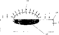
Many semiconductor device can utilize the different doped regions of identical conduction type (p or n) to carry out the better performance of device.Form these different doped regions and mean the additional process steps that increases production cost usually.There is shown typical semiconductor device 1 overlooking of Fig. 1, this device can be a barrier-layer cell, is sometimes referred to as solar cell.The Semiconductor substrate 2 of first doping type has the surface doping district 5 that is generally second doping type and is positioned at metallization pattern 3 at least one first type surface.Metallization pattern 3 generally includes elongated metal electrode 4, between these electrodes and below be doped regions 5 such as emitter, collector electrode or gate regions for example.Electrode 4 can form ohmic contact with the heavily doped region 6 (preferably shown in Fig. 3 and 4) of following substrate 2.Electrode 4 is collected from the electric current in zone 5 or electric current is provided for zone 5, and zone 5 can comprise semiconductor device.For solar cell, zone 5 is generally emitter region.
Solar cell generally is subjected to the influence of the loss of emitter region 5.In order to optimize performance, doped level in the emitter region 5 should be in low level to optimize the collection and the conversion of photon, and zone 6 should be heavy doping and the degree of depth and mixes, to provide good Ohmic contact to metallization pattern 4 not can with the knot 8 (seeing Fig. 2,3) in parallel of burying.Can be by selecting the incompatible optimization whole system of the best group cost of low manufacturing cost and device loss.
Same emitter/the collector design of solar cell schematically is shown in the profile of Fig. 2, and it has preceding hard contact 4, back of the body hard contact 9, diffusion region 7 and ties 8.Same diffusion region 7 on the whole front combines with low-cost metallization technologies such as filament plate printing such as preceding hard contact 4 and causes sizable efficiency losses.This is because in the emitter/collector area 5 of centre, and the distribution (profile) (concentration of doping surfaces reaches from this surface to the emitter/collector electrode degree of depth of knot 8) that forms the required diffusion region 7 of good ohmic contact with this metallization technology is unfavorable for light being converted to electric energy.
Typical same emitter/collector electrode operation is usually included in structure and chemically prepares wafer surface, diffusing step (impurity is from the interior diffusion on surface), oxide passivation step, anti-reflective coating step (TiO for example arbitrarily arbitrarily
2Or Si
3N
4), these steps can provide additional passivation and metallization sequence (preferably by the filament plate printing).
Improvement shown in Figure 3 is, zone 5 is etched into such degree of depth, thereby forms selective emitter/collector area.Emitter/collector electrode refers to that the degree of depth of the doped layer between (finger) 4 has reduced, thereby doped level has also reduced.People such as Szlufeik are at Appl.Phys.Lett.Vol.59; Issue 13; pp1583-1584, the literary composition of " the Simple integral screenprinting process for selectiveemitter polycrystalline silicon solar cells " in 1991 and in 44 01 No. 782 patents of DE (wherein local etching is carried out in the diffusion region between the protection of hard contact protected seam back is to emitter), described this device.Add that protective layer (being generally polymer paste) needs extra masks.The shortcoming of a kind of technology in back is the etching step that needs extra mask and difficulty, has increased complexity and the cost made like this.
Fig. 4 illustrates more effective selective emitter/collector electrode scheme with profile with illustrating, dark emitter/collector electrode dopant profiles the district 6 of high surface doping concentration is wherein arranged below preceding hard contact 3 and shallow dopant profiles, optimize the carrier collection in the adjacent area 5 like this.Yet as mentioned above, the structure of selective emitter/collector electrode needs more complicated manufacturing process, and for example in DE 42 17428, the shallow emitter layer of diffusion then forms passivation/oxide layer on the whole front surface of substrate.Then, use laser beam to form opening in oxide layer, oxide layer is used as the mask that the emitter contact zone is carried out dark diffusing step.Then, in raceway groove, form hard contact 3,4 by the laser opening.
From EP-A-680 099, known a kind of like this solar cell, thus it is included in a n type layer that forms on the entire upper surface of p type silicon substrate, the impurity concentration that forms and is higher than the p type layer of impurity concentration of substrate and the 2nd n type layer that connects a n type layer and p type layer that forms in the side of substrate at least on the back side of substrate.The impurity concentration of the 2nd n type layer is lower than the impurity concentration of a n type layer around the zone that contacts with p type layer, and the outdiffusion in liquid impurity source that can be by being added to the silicon substrate upper surface forms.
US 4,152, and 824 have described the method for solar cell that a kind of production has the shallow/dark junction device structure of mixing.The preceding energy of this solar cell receives a side and has latticed contact, and each part of each contact is consistent, promptly aims at dark interface when shallow junction region is exposed to incident radiation.Form the knot and the contact of mixing by the method that is beneficial to routine techniques, note, the oxide-film that mixes as the diffuse source of composition, implementation gaseous diffusion on the substrate that exposes and form the high doped district.
GB1,470,241 describe a kind of photocell, and it is included in a n who forms under collector electrode grid or the electrode
+District and and n
+Compare heavy doping still less and thinner and at n
+The 2nd n that forms in the space of district's grid
-The district.Form these n by known technologies such as optionally double diffusion, mask and/or photograph
+And n
-The district.
The manufacture method of known use such as the selective emitter/collector electrode of low-cost metallization technologies such as filament plate printing needs second diffusing step and/or mask and/or etching step, thereby causes making metallization pattern 3 to be aimed at the higher doped 6 of semiconductor device 1 front.
The R.J.Overstraeten of Adam Higler Co., Ltd and R.P.Mertens have described the conventional method that forms photovoltaic device in " Physics, technology and use of Photovoltaics ", here introduce by reference.
Summary of the invention
In claim 1 to 13, defined according to manufacture method of the present invention.In claim 14 to 24, defined according to semiconductor device of the present invention.
The present invention be mainly used on Semiconductor substrate form have different level of doping two different selectively diffused regions.Compare with same emitter/collector structure, realized this favourable design of selective emitter or collector structure and without any need for additional processing step or make technology become complicated.Best process sequence is to utilize the filament plate printing to stick with paste to form diffusion region and filament plate type metal paste by first high temperature heat treatment step to provide metallization by second high temperature heat treatment step based on the impurity of solid.
For example, for photovoltaic device, can have with the processing step of typical same emitter/collector electrode technology similar number and than conventional selective emitter/collector electrode technology step still less according to selective emitter of the present invention or collector electrode technology.Method of the present invention provides a kind of simple and economic photovoltaic device manufacture method, makes these devices have the result who is better than known same emitter/collector structure.Compare with same emitter/collector electrode technology need be still less the impurity raw material, thereby reduced production cost and improved final battery performance simultaneously.
The present invention is the simplification that known selective emitter or collector electrode form process sequence.Only in a diffusing step, form according to selective emitter of the present invention or collector structure.Do not need extra mask and/or etch process step to form selective emitter or collector electrode.
Description of drawings
Fig. 1 illustrates the diagrammatic top view of known semiconductor device.
Fig. 2 illustrates the schematic section of the known solar cell with same emitter/collector structure.
Fig. 3 illustrates the schematic section of the known solar cell with selective emitter/collector structure.
Fig. 4 illustrates the schematic section of the another kind of known solar cell with selective emitter/collector structure.
Fig. 5 to 10 illustrates the signal step according to the manufacturing semiconductor device of one embodiment of the present of invention.
Figure 11 schematically illustrates according to direct and indirect diffusion technology of the present invention.
Figure 12 illustrates the figure according to the resistance extending transversely of semiconductor device of the present invention.
Figure 13 to 16 illustrates the signal step according to the manufacturing semiconductor device of another embodiment of the present invention.
Embodiment
Following, will and describe the present invention with reference to the accompanying drawings with reference to some specific embodiment, but the invention is not restricted to this and only limit by claims.In the drawings, for clear, may amplify for example some size such as thickness of layer.Especially, will the present invention be described with reference to photovoltaic device (being sometimes referred to as solar cell), but the invention is not restricted to this that it can be applicable to the ordinary semiconductor device.In addition, main reference is formed different n++-in p type substrate and the present invention is described in n+-type district.The invention is not restricted to this.Method of the present invention can be applicable to form different p type districts or is not forming n++-and n+-type district or forming p++-and p+-type district in doping or the p type substrate in doping or the n type substrate in n type substrate.In addition, main reference single face solar cell illustrates the present invention, but the present invention can be advantageously applied to double-sided solar battery equally.
Only with a high-temperature step and do not use etching or mask technique, use to form the emitter or the collector electrode that for example have different doped regions according to simple process of the present invention and be not limited to solar cell.This technology can be used for other microelectronics production technology, as long as the lateral dimension of doped region and hard contact and diffusion profile have similar tolerance limit.Can realize various types of photodetectors and miniature engineering transducer, thermal conversion semiconductor device and all types of semiconductor device that reduce such as production costs such as thyristors by using according to method of the present invention.
Fig. 5 to 10 schematically illustrates the foundation that is applied to solar cell 1 selective emitter of the present invention or collector electrode manufacturing process.According in the low cost production thereof of the present invention, can when cutting semiconductor substrate 2, begin to handle.Substrate 2 can have monocrystalline, polycrystalline or amorphous silicon.The quality of substrate can be lower than the required quality of transistor device, for example solar energy grade (grade) silicon that disclosed in " Solar cells " 1992 of the Martin Green of New South Wales university.Do not wish the size of substrate 2 is limited, this size will be according to commercially available material.At present, used thickness is the silicon substrate of 10cm * 10cm of 200 to 400 microns, but the invention is not restricted to this.Foundation substrate 2 of the present invention is silicon preferably, but the invention is not restricted to this.Substrate can be GaAs or any other similar Semiconductor substrate 2, and they need the different adjacent diffusing, doping district of doped level selectivity.
At first, Semiconductor substrate 2 being carried out chemically cleaning, then for example at 80 ℃, is that 40% solution carried out etching 2 to 4 minutes to substrate 2, the damage when cutting the surface to remove with the percentage by weight of NaOH in deionization (deionised) water (DI water).Then substrate is cleaned to 8MOhmcm in DI water.Perhaps, as Willeke and Fath at Proc.13th European Photovoltaic Solar Energy Conf.and Exhibition, France, described in " Texturization methods formulticrystalline silicon solar cells " literary composition of 23-27 Oct.1995, can machinery or chemical mode structures (texture) such as pyramid structure for example are provided at one or two first type surface of substrate 2.For example, for this reason, suitably etching is included in 90 ℃, and volume is etching 10 minutes in the solution of the NaOH of 1.3wt% and 5% isopropyl alcohol in DI water.After etching, use DI water as above that substrate 2 is carried out chemically cleaning and cleaning.In the drawings, for clear, omitted structure.
According to the present invention, form heavy doping deep diffusion district 12 (Fig. 8 and 9) in the front surface contact zone below 20, and will form shallow light dope emitter or collector electrode 15 (Fig. 6) elsewhere.Shown in Fig. 5 signal, installation can be adopted definite pattern of linear and/or regional shape, the impurity source 11 based on solid of pasty state that comprises suitable impurity or similar type optionally is added on the first type surface of substrate 2.Sticking with paste 11 some zone that optionally is added on the substrate surface, in step afterwards, form deep diffusion district 12 in these zones.Can use various technology that impurity is stuck with paste 11 optionally is added on the substrate 2.But preferably to determine very much carrying out applying of impurity paste 11 with the mode of duplication of production.Write with a brush dipped in Chinese ink preferable technology such as (writing) such as filament plate printing, print through (offset), photogravure, ink jet printing or paste and have good repeatability.Preferably to print on the substrate sticking with paste 11, in the high technology of output, to provide good repeatability such as thick film technologies such as filament plate printings.Because the front surface metallization pattern 20 (Fig. 8 and 9) that must be added to substrate 2 is afterwards stuck with paste 11 dark district 12 and aimed at formerly adding impurity, be very favorable with the front metal 18 identical technology of sticking with paste so use adds impurity paste 11.The good repeatability of filament plate printing makes and can use subsequently and add that the filament plate of the constructed and same type of sticking with paste 11 (Fig. 5) adds that metal paste 18 forms front surface metallization pattern 20 (Fig. 8).Can use DEK type 1760RS filament plate printer to add and stick with paste 11.
According to the conduction type and the chemical property of substrate 2, can use the paste 11 that comprises such as impurity sources such as P, B, As.When substrate 2 for silicon and when having the p type electric conductivity, can use described in No. 108 065, EP-0 the paste that comprises phosphorus 11 or such as from Belgium Soltech NV) commercially available pastes such as P101.In addition, when substrate 2 for silicon and when having the n type electric conductivity, stick with paste 11 and can comprise boron or aluminium.Utilize p type crystallization Si substrate 2 and phosphorus impurities source to form n type emitter 12,15 in front according to preferable low-cost solar battery manufacturing process of the present invention.
Should so select to stick with paste 11 viscosity, thereby can be added to exactly and stick with paste 11 on the substrate 2 and flow significantly or extend sticking with paste 11 by suitable technology such as for example filament plate printing.Paste 11 is (thixotropic) of thixotroping preferably.Impurity stick with paste 11 viscosity preferably be high enough to prevent to be dry before or tangible lateral flow takes place between dry period or during heat treatment step, otherwise that this lateral flow will cause added impurity to stick with paste 11 line or zone will be wideer than the width of later added front surface hard contact 20.Yet, may want to be widened to slightly sticking with paste 11 line or zone that surpass will be in the line or the zone of the original plan that is covered by hard contact 20 subsequently, thereby avoid tying 8 in parallel with hard contact 20.Permitted to add in the content subsequently hard contact 20 what determine, stuck with paste line and zone 11 preferably slightly greater than subsequently hard contact zone and line 20, thus can repeat and realize exactly the metal paste line and regional 18 with the aiming at of degree of depth doped region 12.
Be preferably in and dryly immediately after applying stick with paste 11.Preferably as far as possible apace the substrate 2 of composition is installed in the drying box, carries out about 1 to 10 minute drying with the paste 11 to thickness under the temperature of (being preferably between 150 and 200 ℃) between 150-350 ℃ therein, with its fixed-site on substrate 2.In order to carry out drying, can use Tempress conveyer belt drier, the infrared banded drier of DEK or similar device.After sticking with paste drying, preferably make the heat treatment step of substrate 2 through two stages.Directly pack into such as in the diffusion chambers such as Tempress/Lindberg conveyer belt diffusion furnace (for example, from Netherlands Gemco) having the dry substrate of sticking with paste 2.In the phase I, be preferably in air or the oxygen atmosphere, stick with paste remaining organic principle in 11 up to about 600 ℃ and the impurity that burnouts for the about 100-150 of per minute elevated temperature ℃.
In second stage, directly send into substrate 2 from the impurity of sticking with paste 11 with the high temperature handle.Be preferably in and carry out this second heat treatment stages in the inert gas atmosphere.Shown in Fig. 6 signal, in this high-temperature step, form degree of depth doped region 12, wherein stick with paste 11 impurity and directly diffuse into just to be arranged in and stick with paste the following substrate 2 of zone and line 11 from impurity.Simultaneously, by being diffused into surrounding atmosphere from impurity 11 indirectly and forming shallow district 15 from the exposed region that surrounding atmosphere is diffused into substrate 2.
Preferably the substrate 2 of composition is placed on being with of can moving horizontally in the banded stove (for example, above-described Tempress/Lindberg conveyer belt diffusion furnace), and remains on such as in the inert gas atmospheres such as nitrogen.Temperature is elevated to 800 to 1100 ℃, preferably 900 to 950 ℃, simultaneously temperature gradient is remained on about 150 ℃/minute.Preferably substrate 2 was remained under this temperature about 10 to 60 minutes.Not only impurity is arranged from sticking with paste the 11 inside diffusions that enter substrate 2 with the substrate 2 tight places that contact sticking with paste 11, also have impurity enter ambient atmosphere (foreign atom can reenter substrate 2 indirectly from this) to outdiffusion.Form second diffusion region 15 near being diffused in the zone that is added with impurity paste 11 indirectly.As shown in figure 11, foreign atom begins along all directions from sticking with paste diffusion 11.Thereby, compare with other zone on following Semiconductor substrate 2 surfaces, sticking with paste 11 and 12 places, zone that directly contact of this substrate 2, substrate 2 has stood strong relatively foreign atom and has inwardly spread.Non-selected property be added with impurity and stick with paste 11 place, impurity is diffused into the substrate 2 from ambient atmosphere.Doping can produce second diffusion layer 15 in substrate 2 indirectly, and the concentration of first diffusion region 12 of its concentration ratio substrate 2 (just be positioned at and be added with the local following of paste 11) is low.During high-temperature step, it is shallow that the low concentration of foreign atom also can cause 15 to the first diffusion regions 12, second diffusion region in substrate 2 ambient atmospheres.The concentration of foreign atom is much lower in the comparable paste 11 of the concentration of the foreign atom in the surrounding atmosphere, and its diffusivity is also much lower as a result.Cause impurity source 11 relative dark like this, and the doped region 15 at substrate-gas interface place is more weak and more shallow with the doped region 12 of substrate 2 contacts.Can optionally control the difference of two diffusion regions by the composition, atmosphere, diffusion time or the diffusion temperature that change the impurity paste.Can optimize these conditions and produce the second shallow diffusion region 15, the degree of depth of first diffusion region 12 should just be enough to form good ohmic front surface hard contact 20 simultaneously, and not in parallel with knot 8.Also can use in the tube furnace (tube furnace) of sealing and use for example POCl
3, gaseous state such as BBr3 impurity atmosphere carry out the diffusion sequence.By second diffusion region 15 being regulated, optionally and independently control the diffusion profile of first and second diffusion regions 12,15 from the direct diffusion of gaseous impurities gas and the relative populations of sticking with paste 11 indirect diffusion from impurity.In addition, can use more than a kind of paste 11 to come in substrate 2, optionally to form different diffusion regions by heat treatment.Different pastes 11 can have different foreign atom concentration, perhaps can comprise dissimilar impurity.In addition, some stick with paste 11 can not comprise foreign atom, and the mask that is spread indirectly as the lower floor that prevents substrate 2 only.
When semiconductor device 1 is barrier-layer cell, the degree of depth of the first dark diffusion region 12 of a formation emitter or a collector area part or the variation of impurity concentration can not produce strong influence to battery performance, and the variation of the second shallow diffusion region 15 may have much bigger influence to battery behavior.Second diffusion region 15 has surface impurity concentration and the degree of depth more much lower than dark district 12 usually.Preferably optimize the doping condition of second diffusion region 15, be beneficial to carrier collection.Carrier collection is sensitive to the impurity concentration and the degree of depth.On the other hand, be added with diffusion stick with paste 12 and with operation afterwards in the place of printed metallization pattern 18, the diffusion of first diffusion region 12 is can only be enough dark and have a sufficiently high surface impurity concentration, thus can emitter or collector area 12 form good Ohmic contacts 20 and not in parallel with knot 8.
According to method of the present invention, can in single doping step, produce the different doped region of the depth.For example, for darker doped region 12, surface impurity concentration can be 10
20Phosphorus atoms/cm
3In the above scope, for more shallow doped region 15, surface impurity concentration is 5 * 10
18To 10
20, usually 1 * 10
19To 5 * 10
19Phosphorus atoms/cm
3In the scope.The degree of depth of the knot of darker doped region 12 is preferably at least 0.3 micron, is more preferably at least 0.5 micron, is typically 0.6 micron, and for more shallow doped region 15, junction depth is up to 0.3 micron, is typically 0.2 micron.Figure 12 illustrates, for foundation J.R.Ehrstein, D.C.Gupta and P.H.Langer at Emerging Semiconductor Technology, ASTM STP 960, the solar cell of the present invention that " Spresing resistiance measurements-An overview " literary composition of Am.Soc.for Test andMat.1986 is carried out produces the resistance scan extending transversely of selective emitter or collector structure.Placing width with the distance of mutual about 3mm is 100 microns paste line 11.Optionally emitter or collector structure have low, the dark and strong diffusion region of resistance 12 in the place that must add metallization 20, and the emitter or the collector area that are absorbed and produce charge carrier at photon have shallow and weak diffusion region 15.As shown in figure 12, this paste causes the distance low-resistance region 12 of narrow size of width (be about himself).Resistance reduces to shallow district 15 dullnesses of the about 1mm of distance.The resistance ratio in depth zone 12,15 surpasses 5, and is about 10 or bigger for solar cell.This is that similar variation by foreign atom concentration in these zones causes.In the device of finishing, dark diffusion region 12 and shallow diffusion region 15 can periodically alternately show precipitous gradient at the place, transition region, and these transition regions are about an order of magnitude difference of foreign atom surface concentration.Impurity concentration is high more, and then resistance is low more.The solar cell latter who finishes, impurity concentration and relevant resistance have reduced to provide good carrier collection performance from weak doping district 15 to the dullness of the degree of depth doped region 12 that will be placed hard contact 20.In the solar cell of finishing, the gradient that the surface concentration of foreign atom increases to the zone that will place hard contact helps charge carrier and collects the transmission of 20 places, contact to these.According to the present invention, can and distinguish the dullness that obtains foreign atom concentration in the surf zone of substrate 2 between 12 in shallow district 15 deeply and increase, the difference of the impurity density in the impurity density in shallow district 15 and the dark district 12 is at least 5 times, and usually an order of magnitude or more than.With compare, with operation of the present invention can produce the efficient of the solar cell that its efficient produced than same emitter or collector electrode technology absolute high>1% solar cell, and do not increase processing step, reduce the cost (impurity source) of diffusion sequence simultaneously.
Behind diffusing step, can in DI water, contain in the chemical etching liquor of the about 25%-50% of HF and remove remaining diffusing glass on the surface of silicon, clean and clean substrate 2 thereafter.The present invention includes and do not remove this diffusing glass and continue oxidation/passivation step.This can be avoided HF acid cleaning, and is favourable to environment.
As shown in Figure 7, then be any oxidation step after the diffusion sequence, wherein, substrate is exposed to the O that is usually located in the quartz evaporating dish (boat) by under the temperature in 800-950 ℃ of scope
2Atmosphere 1-20 minute, thus on avoiding, substrate forms SiO
2Layer 16a and 16b.This SiO
2Layer 16a, 16b become the defective in the surface emitting utmost point/collector region 15 of passivation substrate 2, and these defectives may reduce Solar cell performance.Use oxide layer to continue passivation and reduced surperficial recombination rates, reduce the charge carrier loss then, thereby improved efficient.Perhaps, not only can add and also can add antireflecting coating (ARC) 17 such as passivation layer 16a, 16b such as oxides.Can pass through chemical vapor deposition (CVD, for example TiO
2Layer) or plasma-enhanced CVD (PECVD, for example silicon nitride layer) or similar techniques add ARC layer 17.Add that the ARC layer can be to the surface and the good passivation of whole formation of Semiconductor substrate.
At last, the metallization sequence generally includes two or three contact print steps: according to different metal what and use front contact 20 and one or two back of the body contacts patterns 21.Shown in Fig. 8 signal, metal paste 18 optionally is added to the front of substrate 2, aim at heavily doped regional 12.Further, metal paste 19 selectivity or non-selectively be added to the back side of substrate 2.Filament plate printing and subsequently drying are the best approaches that adds these contacts, yet, also can use above-described other thick film technology or evaporation or from the metal plating of the aqueous solution.Each print steps is all followed the drying steps of the moderate temperature about 250 degrees centigrade, for example passes through infrared heater.As shown in Figure 9, then, sintering metal is stuck with paste 18,19 about 30 to 200 seconds under the high temperature in 650 to 900 degrees centigrade of scopes, forms good ohm contacts 20 not in parallel with knot 8 with the front at substrate 2, and forms good ohmic contact 21 at the back side of substrate 2.By any ARC or oxide layer 16b; 17 form contact 20 and 21.Peak temperature and Temperature Distribution (temperature is to the time) are extremely important, and they must be adapted to each metallization paste and operation respectively.Usually, after being separated drying, in a high-temperature step, front and the b contact that is printed with metal paste 18,19 by filament plate carried out sintering.Perhaps, as shown in Figure 9, form back surface field (BSF) layer 22 at the back side of substrate 2 simultaneously.In order to form BSF 22, be preferably and form back metal contact 21 and use high temperature and aluminium paste.
Perhaps, as shown in figure 10, can after metallization, add anti-reflective coating (ARC) layer 23, rather than added with reference to figure 8 described ARC layers 17 before metallization.Typical A RC layer can comprise TiO2, Si
3N
4Or Ta
2O
5Or materials similar, and can add by various technology.Can use hard contact sintering temperature to form the contact up to 800 ℃, and not in parallel with knot 8.When aluminium was used for hard contact, the sintering under this high temperature had such as extra advantages such as Al degasification and BSF formation.
Be used to add that such as filament plate printing etc. the metal and/or the thick film technology of sticking with paste of mixing show good repeatability.Can utilize the navigation system of ccd video camera control, by the filament plate printing machine substrate 2 be installed to same position under the filament plate at every turn.If utilized in first diffusion region 12 of the broad slightly of microscopically different color and added oxide and/or ARC layer 16a, 16b; 17,23, then may command different metalization and diffusion patterned aligning.By deposit ARC layer 17,23, substrate 2 shows different colors in the place that substrate has higher impurity surface concentration.This is that following oxide layer 16b grows thicklyer in the higher place of impurity surface concentration because compare with oxide layer 16a on the lower zone 15 of doped level.As long as add anti-reflective coating (ARC) layer 17 or 23, just can find out following pattern.Its reason is, the higher local oxidation of impurity surface concentration is very fast, causes oxide layer 16 thicker.After adding ARC layer 17 or 23,, make the difference of oxide thickness become obvious because layer 16b+17 or 23 compares the optical thickness difference of color then with 16a+17 or 23.
Can form selective emitter/collector electrode solar cell that battery performance (collection efficiency) improves according to simple procedures of the present invention, and not make technology become complicated or the increase production cost.The result more saves the local solar cell of producing.Owing to used filament plate printing diffusion, so do not need extra or complicated treatment facility.Simultaneously, permitted content by using selective emitter can increase technology.For example the variation in the medium different technical parameters of metallization sintering step is not so good as in same emitter or the collector electrode technology so important.This causes higher craft rate of production, thereby makes technology more save cost.
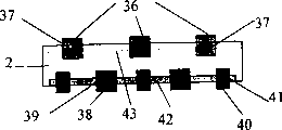
Figure 13 to 16 schematically illustrates the manufacturing step according to the semiconductor device 30 of another embodiment of the present invention.Described one embodiment of the present of invention in detail with reference to figure 5 to 10, will another embodiment be described in detail.Except main doping step, will other details that form passivation layer, cleaning and this technology be described no longer.The technology of another embodiment is adapted to form photovoltaic device.
As shown in figure 13, mix to stick with paste pattern 31 to first and optionally be added on the Semiconductor substrate 2, substrate 2 can be silicon substrate and can be unadulterated or can have the p type or the n conductivity.Can add by previous described any thick film technology and stick with paste 31.The dry then pattern 31 of sticking with paste.First impurity sticks with paste 31 can have first or second conductivity.Can at random protect first to stick with paste pattern 31 by adding other material of last layer (for example another layer sticks with paste 32).Paste 32 can have and stick with paste 31 different concentration or types, perhaps can be unadulterated.Can be added on the first type surface of substrate 2 sticking with paste 32.The dry then layer 32 of sticking with paste.
As shown in figure 14, also can stick with paste another first type surface that pattern 33 optionally is added to substrate 2 to the 3rd.The dry then pattern of sticking with paste.Stick with paste 33 and can have first or second conductivity.Can protect other selected part on the surface of sticking with paste pattern 33 and substrate 2 by optionally adding unadulterated material 34, this material 34 can be to stick with paste.Can add by above-described any thick film technology and stick with paste 34.The dry then pattern 34 of sticking with paste.
As shown in figure 15, can optionally be added to the paste pattern 35 of another doping the first type surface of substrate 2.Paste 35 can comprise the impurity of any conductivity type.Can add by any thick film technology shown in above and stick with paste 35.Dry then paste 35.
Then, the substrate 2 of composition is placed in the stove, being sent in the substrate 2, to form doped layer 37,39 and 41 respectively from for example impurity that comprise those pastes of foreign atom such as 31,33,35.Simultaneously, the foreign atom of sticking with paste from non-protection be diffused into indirectly substrate not protected regional 42 in, to form shallow weak doping district 42.At last, add that metal paste makes it 37,39 or 41 to aim at the zone, and sintering at high temperature, to form hard contact 36,38 or 40 respectively.
In the technology of another embodiment, contact 2 can be a p type silicon, and sticking with paste 31,35 or 32 can be phosphorous paste, and sticking with paste 33 can be the paste of boracic or aluminium, and it can be unadulterated sticking with paste 34.When layer 32 comprised a kind of impurity, high temperature transmitted the doped region 43 (being represented by dotted lines) between the high doped district 37 on first first type surface that (drive-in) step causes forming Semiconductor substrate in Figure 16.Perhaps, the protection that can omit in Figure 13 and 14 sticks with paste 32, causes forming the weak doping district 43 (being represented by dotted lines) that spreads indirectly between the high doped district 37 after the transfer step in Figure 16.Change as another, can omit the layer 32 and 31 among Figure 14, cause, thereby form the floating boom knot at the indirect diffusion layer 43 (in Figure 16, being represented by dotted lines) that forms whole first first type surface of crossing over Semiconductor substrate after the transfer step.
The device that single diffusing step was produced with the foundation another embodiment of the present invention can be selective in the above emitter and the solar cell that the floating boom knot is arranged overleaf.This photovoltaic device can show than the better battery performance of single face battery that has conventional back face metalization on the whole back side.The device that method produced by another embodiment also can be used as double-sided solar battery.
The advantage that technology had according to another embodiment is to produce the solar cell with efficiency value and short circuit current raising by better emitter/collector structure and better back of the body contact.Back of the body contact not metallization on the whole back of the body first type surface of substrate 2 according to another embodiment causes better backside reflection or it to can be used for two-sided battery design.
Though more than described preferred embodiment of the present invention in detail, be appreciated that the one skilled in the art can carry out many changes and modification and do not deviate from scope and spirit of the present invention.
Claims (29)
1. a manufacturing comprises the method for the semiconductor device of flaky semiconductor substrate, it is characterized in that this method may further comprise the steps:
Step 1) optionally is added to first first type surface of described Semiconductor substrate to the pattern based on the impurity source of solid, to form on first first type surface by the described zone that covers based on the impurity of solid with not by the zone of described impurity covering based on solid;
Step 2) under the gaseous environment that surrounds described Semiconductor substrate, by controlled heat treatment step foreign atom is diffused into the described substrate from described impurity source based on solid, impurity directly is diffused into the described substrate with the described substrate below the described pattern that just is arranged in described impurity source based on solid from described impurity source based on solid and forms first diffusion region, simultaneously, described impurity is diffused into the described substrate via described gaseous environment indirectly from described impurity source based on solid, with described substrate not by at least some zones of described pattern covers in form second diffusion region; And
Step 3) forms the hard contact pattern of aiming at described first diffusion region basically, and need not described second diffusion region of etching basically.
2. the method for claim 1 is characterized in that the described step 1) of optionally adding comprises the impurity source of optionally deposit based on solid.
3. method as claimed in claim 1 or 2 is characterized in that described substrate is first conductivity type, and the impurity of described impurity source based on solid is second conductivity type.
4. the method for claim 1 is characterized in that also being included in described diffusing step 2) back and the step that before described hard contact forms step 3), adds passivation layer.
5. method as claimed in claim 4 is characterized in that described passivation layer is an oxide layer.
6. the method for claim 1 is characterized in that also being included in the selectivity impurity source and adds the step that step 1) is constructed described Semiconductor substrate before.
7. the method for claim 1 is characterized in that described impurity source based on solid is to print added first by filament plate to stick with paste.
8. the method for claim 1 is characterized in that also comprising the step of adding antireflecting coating.
9. method as claimed in claim 4 is characterized in that the described step 3) that forms the hard contact pattern comprises that the sintering by described passivation and/or described antireflecting coating forms ohmic contact between described hard contact pattern and described first diffusion region.
10. the method for claim 1, it is characterized in that described selectivity impurity source adds step 1) and comprises and being added on one or more first type surfaces of described substrate based on the material of solid to one or more other, to be conductivity identical with the conductivity of described impurity source based on solid but other impurity source that concentration is different for every kind of described other material based on solid, or another kind of conductivity type or unadulterated other impurity source.
11. the method for claim 1 is characterized in that the described step that forms second diffusion region forms emitter or collector area in described Semiconductor substrate.
12. the method for claim 1 is characterized in that described second diffusion region is wideer than described first diffusion region basically.
13. the method for claim 1 is characterized in that the ratio of doped level in described first and second zones is at least 5.
14. method as claimed in claim 13 is characterized in that the ratio of doped level in described first and second zones further is about 10 or bigger.
15. a photovoltaic device is characterized in that comprising: the Semiconductor substrate of sheet, be arranged in first and second doped regions of a first type surface of Semiconductor substrate; Compare with second doped region, the first surface of adulteration area impurity concentration is higher; And the hard contact pattern of aiming at described first diffusion region basically, the wherein said second surface of adulteration area impurity concentration along with in described second doped region to the distance of described first doped region and increase, the increase gradient spacing of the surface concentration gradient of impurity is at least 0.5mm, helps charge carrier and transmits to the hard contact pattern along the length direction of described second doped region.
16. photovoltaic device as claimed in claim 15, the increase that it is characterized in that surface impurity concentration is dull.
17., it is characterized in that the increase of surface impurity concentration accounts for the distance of about 1mm as claim 15 or 16 described photovoltaic devices.
18. photovoltaic device as claimed in claim 15 is characterized in that described substrate is first conductivity type, the impurity of described first doped region is second conductivity type.
19. photovoltaic device as claimed in claim 15 is characterized in that also comprising the passivation layer that is positioned on described first and second doped regions.
20. photovoltaic device as claimed in claim 19 is characterized in that described passivation layer is an oxide layer.
21. photovoltaic device as claimed in claim 15 is characterized in that constructing the surface of described Semiconductor substrate.
22. photovoltaic device as claimed in claim 15 is characterized in that also comprising antireflecting coating.
23. photovoltaic device as claimed in claim 15 is characterized in that described second doped region forms emitter or collector area in described Semiconductor substrate.
24. photovoltaic device as claimed in claim 15 is characterized in that the ratio of surface impurity concentration between described first and second doped regions is at least 5.
25. photovoltaic device as claimed in claim 24 is characterized in that the ratio of surface impurity concentration between described first and second doped regions further is about 10 or bigger.
26. photovoltaic device as claimed in claim 15 is characterized in that second doped region has the uniform basically middle section of surface impurity concentration.
27. photovoltaic device as claimed in claim 15 is characterized in that described hard contact pattern and described first doped region form ohmic contact.
28. photovoltaic device as claimed in claim 15, it is characterized in that under the gaseous environment that surrounds described Semiconductor substrate, by controlled heat treatment step foreign atom is diffused into from the impurity source based on solid and form first and second doped regions the described substrate, impurity directly diffuses into the described substrate describedly to form first doped region based on the described substrate below the impurity source of solid just being arranged in from described impurity source based on solid, simultaneously, described impurity diffuses into the described substrate to form second doped region via described gaseous environment indirectly from described impurity source based on solid.
29. method as claimed in claim 15 is characterized in that described semiconductor device is a barrier-layer cell.
Applications Claiming Priority (2)
| Application Number | Priority Date | Filing Date | Title |
|---|---|---|---|
| EP96120865.9 | 1996-12-24 | ||
| EP96120865A EP0851511A1 (en) | 1996-12-24 | 1996-12-24 | Semiconductor device with two selectively diffused regions |
Publications (2)
| Publication Number | Publication Date |
|---|---|
| CN1241298A CN1241298A (en) | 2000-01-12 |
| CN1155104C true CN1155104C (en) | 2004-06-23 |
Family
ID=8223558
Family Applications (1)
| Application Number | Title | Priority Date | Filing Date |
|---|---|---|---|
| CNB971808910A Expired - Lifetime CN1155104C (en) | 1996-12-24 | 1997-12-22 | Semiconductor device with selectively diffused regions |
Country Status (10)
| Country | Link |
|---|---|
| EP (2) | EP0851511A1 (en) |
| JP (2) | JP3999820B2 (en) |
| CN (1) | CN1155104C (en) |
| AT (1) | ATE281698T1 (en) |
| AU (1) | AU741153B2 (en) |
| CA (1) | CA2276008C (en) |
| DE (1) | DE69731485T2 (en) |
| DK (1) | DK0960443T3 (en) |
| ES (1) | ES2232887T3 (en) |
| WO (1) | WO1998028798A1 (en) |
Families Citing this family (75)
| Publication number | Priority date | Publication date | Assignee | Title |
|---|---|---|---|---|
| JP2000138386A (en) * | 1998-11-04 | 2000-05-16 | Shin Etsu Chem Co Ltd | Manufacturing method of solar cell and solar cell manufactured by the method |
| EP1024523A1 (en) * | 1999-01-27 | 2000-08-02 | Imec (Interuniversity Microelectronics Center) VZW | Method for fabricating thin film semiconductor devices |
| NL1012961C2 (en) | 1999-09-02 | 2001-03-05 | Stichting Energie | A method of manufacturing a semiconductor device. |
| KR100420030B1 (en) * | 2001-04-23 | 2004-02-25 | 삼성에스디아이 주식회사 | Method for manufacturing solar cell |
| GB0114896D0 (en) * | 2001-06-19 | 2001-08-08 | Bp Solar Ltd | Process for manufacturing a solar cell |
| EP1378947A1 (en) | 2002-07-01 | 2004-01-07 | Interuniversitair Microelektronica Centrum Vzw | Semiconductor etching paste and the use thereof for localised etching of semiconductor substrates |
| JP4121928B2 (en) | 2003-10-08 | 2008-07-23 | シャープ株式会社 | Manufacturing method of solar cell |
| JP4232597B2 (en) | 2003-10-10 | 2009-03-04 | 株式会社日立製作所 | Silicon solar cell and manufacturing method thereof |
| JP2006073617A (en) * | 2004-08-31 | 2006-03-16 | Sharp Corp | Solar cell and manufacturing method thereof |
| US7906722B2 (en) | 2005-04-19 | 2011-03-15 | Palo Alto Research Center Incorporated | Concentrating solar collector with solid optical element |
| US7765949B2 (en) | 2005-11-17 | 2010-08-03 | Palo Alto Research Center Incorporated | Extrusion/dispensing systems and methods |
| US7799371B2 (en) | 2005-11-17 | 2010-09-21 | Palo Alto Research Center Incorporated | Extruding/dispensing multiple materials to form high-aspect ratio extruded structures |
| US20070107773A1 (en) | 2005-11-17 | 2007-05-17 | Palo Alto Research Center Incorporated | Bifacial cell with extruded gridline metallization |
| WO2007059577A1 (en) | 2005-11-24 | 2007-05-31 | Newsouth Innovations Pty Limited | Metallisation method for thin-film semiconductor structures |
| US7820475B2 (en) | 2005-12-21 | 2010-10-26 | Sunpower Corporation | Back side contact solar cell structures and fabrication processes |
| US7851693B2 (en) | 2006-05-05 | 2010-12-14 | Palo Alto Research Center Incorporated | Passively cooled solar concentrating photovoltaic device |
| US8226391B2 (en) | 2006-11-01 | 2012-07-24 | Solarworld Innovations Gmbh | Micro-extrusion printhead nozzle with tapered cross-section |
| US7922471B2 (en) | 2006-11-01 | 2011-04-12 | Palo Alto Research Center Incorporated | Extruded structure with equilibrium shape |
| US8322025B2 (en) | 2006-11-01 | 2012-12-04 | Solarworld Innovations Gmbh | Apparatus for forming a plurality of high-aspect ratio gridline structures |
| US7780812B2 (en) | 2006-11-01 | 2010-08-24 | Palo Alto Research Center Incorporated | Extrusion head with planarized edge surface |
| US7638438B2 (en) | 2006-12-12 | 2009-12-29 | Palo Alto Research Center Incorporated | Solar cell fabrication using extrusion mask |
| US7928015B2 (en) | 2006-12-12 | 2011-04-19 | Palo Alto Research Center Incorporated | Solar cell fabrication using extruded dopant-bearing materials |
| EP2122691A4 (en) | 2007-02-16 | 2011-02-16 | Nanogram Corp | Solar cell structures, photovoltaic modules and corresponding processes |
| US7954449B2 (en) | 2007-05-08 | 2011-06-07 | Palo Alto Research Center Incorporated | Wiring-free, plumbing-free, cooled, vacuum chuck |
| WO2009010585A2 (en) * | 2007-07-18 | 2009-01-22 | Interuniversitair Microelektronica Centrum Vzw | Method for producing an emitter structure and emitter structures resulting therefrom |
| JP2010534927A (en) * | 2007-07-26 | 2010-11-11 | ウニベルジテーツ コンスタンツ | Silicon solar cell having emitter with back-etching and method of forming similar solar cell |
| DE102007035068A1 (en) * | 2007-07-26 | 2009-01-29 | Fraunhofer-Gesellschaft zur Förderung der angewandten Forschung e.V. | Method for manufacturing silicon solar cell with selective emitter, involves producing laminar emitter at emitter surface of solar cell substrate and applying corroding barrier on sub ranges of emitter surface |
| JP5236914B2 (en) * | 2007-09-19 | 2013-07-17 | シャープ株式会社 | Manufacturing method of solar cell |
| US8222516B2 (en) * | 2008-02-20 | 2012-07-17 | Sunpower Corporation | Front contact solar cell with formed emitter |
| AU2008359970A1 (en) * | 2008-07-28 | 2010-02-04 | Day4 Energy Inc. | Crystalline silicon PV cell with selective emitter produced with low temperature precision etch back and passivation process |
| JP5344872B2 (en) * | 2008-08-27 | 2013-11-20 | 三菱電機株式会社 | Photovoltaic device |
| US7999175B2 (en) | 2008-09-09 | 2011-08-16 | Palo Alto Research Center Incorporated | Interdigitated back contact silicon solar cells with laser ablated grooves |
| US8117983B2 (en) | 2008-11-07 | 2012-02-21 | Solarworld Innovations Gmbh | Directional extruded bead control |
| US9150966B2 (en) | 2008-11-14 | 2015-10-06 | Palo Alto Research Center Incorporated | Solar cell metallization using inline electroless plating |
| US8080729B2 (en) | 2008-11-24 | 2011-12-20 | Palo Alto Research Center Incorporated | Melt planarization of solar cell bus bars |
| US8960120B2 (en) | 2008-12-09 | 2015-02-24 | Palo Alto Research Center Incorporated | Micro-extrusion printhead with nozzle valves |
| JP5029921B2 (en) * | 2009-01-19 | 2012-09-19 | シャープ株式会社 | Method for manufacturing solar battery cell |
| DE102009018653B4 (en) * | 2009-03-04 | 2015-12-03 | SolarWorld Industries Thüringen GmbH | Method for the production of semiconductor devices using doping techniques |
| DE102009041546A1 (en) | 2009-03-27 | 2010-10-14 | Bosch Solar Energy Ag | Process for the production of solar cells with selective emitter |
| KR101597825B1 (en) * | 2009-07-24 | 2016-02-25 | 엘지전자 주식회사 | Solar Cell Method for solar cell and Heat Treatment Apparatus for Thermal Diffusion |
| NL2003324C2 (en) * | 2009-07-31 | 2011-02-02 | Otb Solar Bv | Photovoltaic cell with a selective emitter and method for making the same. |
| KR101611456B1 (en) * | 2009-09-02 | 2016-04-11 | 엘지이노텍 주식회사 | Paste composition for manufacturing solar-cell electrode comprising phosphoric dispersant |
| US8735234B2 (en) | 2010-02-18 | 2014-05-27 | Varian Semiconductor Equipment Associates, Inc. | Self-aligned ion implantation for IBC solar cells |
| WO2011110231A1 (en) * | 2010-03-12 | 2011-09-15 | Q-Cells Se | Method and in-line production system for the production of solar cells |
| KR101046219B1 (en) | 2010-04-02 | 2011-07-04 | 엘지전자 주식회사 | Solar cell having a selective emitter |
| CN101866971A (en) * | 2010-05-18 | 2010-10-20 | 常州亿晶光电科技有限公司 | Broken solar cells with selective emitting stage |
| CN101866984B (en) * | 2010-05-18 | 2015-01-07 | 常州亿晶光电科技有限公司 | Method for selectively doping emitting stage on surface of crystalline silicon cell film |
| JP5734734B2 (en) * | 2010-05-18 | 2015-06-17 | ローム アンド ハース エレクトロニック マテリアルズ エルエルシーRohm and Haas Electronic Materials LLC | Method for forming current tracks on a semiconductor |
| DE102010024308A1 (en) * | 2010-06-18 | 2011-12-22 | Fraunhofer-Gesellschaft zur Förderung der angewandten Forschung e.V. | Method for producing a selective doping structure in a semiconductor substrate for producing a photovoltaic solar cell |
| JP5538103B2 (en) * | 2010-07-07 | 2014-07-02 | 三菱電機株式会社 | Method for manufacturing solar battery cell |
| US20110139231A1 (en) * | 2010-08-25 | 2011-06-16 | Daniel Meier | Back junction solar cell with selective front surface field |
| KR101733055B1 (en) * | 2010-09-06 | 2017-05-24 | 엘지전자 주식회사 | Solar cell module |
| CN102468364A (en) * | 2010-11-05 | 2012-05-23 | 无锡尚德太阳能电力有限公司 | Selective emitting electrode solar cell and manufacturing method thereof |
| KR20130129919A (en) * | 2010-11-17 | 2013-11-29 | 히타치가세이가부시끼가이샤 | Method for producing solar cell |
| CN102110721A (en) * | 2010-12-17 | 2011-06-29 | 福建省上杭县九洲硅业有限公司 | Gradient type back surface field of polycrystalline silicon solar cell and preparation method thereof |
| CN102082210A (en) * | 2010-12-18 | 2011-06-01 | 广东爱康太阳能科技有限公司 | Method for manufacturing fine grid selective emitter crystalline silicon solar cell |
| KR101198438B1 (en) | 2010-12-31 | 2012-11-06 | 현대중공업 주식회사 | Bifacial Photovoltaic Localized Emitter Solar Cell and Method for Manufacturing Thereof |
| KR101114198B1 (en) | 2010-12-31 | 2012-03-13 | 현대중공업 주식회사 | Localized emitter solar cell and method for manufacturing thereof |
| DE102011002748A1 (en) | 2011-01-17 | 2012-07-19 | Robert Bosch Gmbh | Process for producing a silicon solar cell |
| US8962424B2 (en) | 2011-03-03 | 2015-02-24 | Palo Alto Research Center Incorporated | N-type silicon solar cell with contact/protection structures |
| KR101071546B1 (en) | 2011-04-26 | 2011-10-10 | 주식회사 톱텍 | Solar cell manufacturing method and the solar cell manufactured using the method |
| DE102011051040A1 (en) * | 2011-06-14 | 2012-12-20 | Solarworld Innovations Gmbh | Method for manufacturing e.g. quadratic solar cell, involves back etching portion of highly doped emitter region between portions of metallization structure by using metallization structure as etching mask |
| CN102306684B (en) * | 2011-09-19 | 2016-01-20 | 苏州旭环光伏科技有限公司 | Selective emitter of a kind of three grades of doped level and preparation method thereof |
| TWI424584B (en) * | 2011-11-30 | 2014-01-21 | Au Optronics Corp | Method of forming solar cell |
| US20130199604A1 (en) * | 2012-02-06 | 2013-08-08 | Silicon Solar Solutions | Solar cells and methods of fabrication thereof |
| US8895325B2 (en) * | 2012-04-27 | 2014-11-25 | Varian Semiconductor Equipment Associates, Inc. | System and method for aligning substrates for multiple implants |
| KR102039611B1 (en) * | 2012-05-22 | 2019-11-01 | 주성엔지니어링(주) | Wafer type solar cell and method for manufacturing thereof, method and apparatus for doping of wafer type solar cell |
| CN102856436A (en) * | 2012-09-05 | 2013-01-02 | 友达光电股份有限公司 | Solar cell and manufacturing method thereof |
| JP6379461B2 (en) * | 2013-09-02 | 2018-08-29 | 日立化成株式会社 | Method for manufacturing silicon substrate having p-type diffusion layer, method for manufacturing solar cell element, and solar cell element |
| US9960287B2 (en) | 2014-02-11 | 2018-05-01 | Picasolar, Inc. | Solar cells and methods of fabrication thereof |
| JP6661891B2 (en) * | 2015-05-07 | 2020-03-11 | 日立化成株式会社 | Method of manufacturing solar cell element and solar cell element |
| JP6270889B2 (en) * | 2016-03-16 | 2018-01-31 | 三菱電機株式会社 | Manufacturing method of solar cell |
| KR102045989B1 (en) | 2018-03-14 | 2019-11-18 | 한국과학기술연구원 | Semiconductor device using interdiffusion and method for manufacturing the same |
| WO2019206679A1 (en) | 2018-04-24 | 2019-10-31 | CSEM Centre Suisse d'Electronique et de Microtechnique SA - Recherche et Développement | Passivated layer stack for a light harvesting device |
| CN113675289B (en) * | 2021-10-22 | 2022-03-01 | 浙江晶科能源有限公司 | Photovoltaic cell, preparation method thereof and photovoltaic module |
Family Cites Families (6)
| Publication number | Priority date | Publication date | Assignee | Title |
|---|---|---|---|---|
| FR2238251B1 (en) * | 1973-07-03 | 1977-09-16 | Telecommunications Sa | |
| US4152824A (en) * | 1977-12-30 | 1979-05-08 | Mobil Tyco Solar Energy Corporation | Manufacture of solar cells |
| US4478879A (en) * | 1983-02-10 | 1984-10-23 | The United States Of America As Represented By The Administrator Of The National Aeronautics And Space Administration | Screen printed interdigitated back contact solar cell |
| DE4217428A1 (en) * | 1991-12-09 | 1993-06-17 | Deutsche Aerospace | High performance silicon crystalline solar cell structure - has more highly doped layer integrated in lightly doped layer in area below metallic contact |
| DE4401782C2 (en) * | 1994-01-21 | 2001-08-02 | Angew Solarenergie Ase Gmbh | Method for producing a locally flat emitter between the contact fingers of a solar cell |
| JP3032422B2 (en) * | 1994-04-28 | 2000-04-17 | シャープ株式会社 | Solar cell and method of manufacturing the same |
-
1996
- 1996-12-24 EP EP96120865A patent/EP0851511A1/en not_active Withdrawn
-
1997
- 1997-12-22 CA CA002276008A patent/CA2276008C/en not_active Expired - Fee Related
- 1997-12-22 ES ES97954669T patent/ES2232887T3/en not_active Expired - Lifetime
- 1997-12-22 CN CNB971808910A patent/CN1155104C/en not_active Expired - Lifetime
- 1997-12-22 DK DK97954669T patent/DK0960443T3/en active
- 1997-12-22 AT AT97954669T patent/ATE281698T1/en active
- 1997-12-22 JP JP52840198A patent/JP3999820B2/en not_active Expired - Lifetime
- 1997-12-22 EP EP97954669A patent/EP0960443B1/en not_active Expired - Lifetime
- 1997-12-22 WO PCT/EP1997/007246 patent/WO1998028798A1/en active IP Right Grant
- 1997-12-22 DE DE69731485T patent/DE69731485T2/en not_active Expired - Lifetime
- 1997-12-22 AU AU59555/98A patent/AU741153B2/en not_active Ceased
-
2007
- 2007-05-25 JP JP2007139083A patent/JP2007235174A/en active Pending
Also Published As
| Publication number | Publication date |
|---|---|
| AU741153B2 (en) | 2001-11-22 |
| WO1998028798A1 (en) | 1998-07-02 |
| JP2002503390A (en) | 2002-01-29 |
| EP0960443A1 (en) | 1999-12-01 |
| EP0960443B1 (en) | 2004-11-03 |
| ES2232887T3 (en) | 2005-06-01 |
| EP0851511A1 (en) | 1998-07-01 |
| CA2276008C (en) | 2005-03-22 |
| ATE281698T1 (en) | 2004-11-15 |
| AU5955598A (en) | 1998-07-17 |
| CN1241298A (en) | 2000-01-12 |
| DE69731485T2 (en) | 2005-10-27 |
| CA2276008A1 (en) | 1998-07-02 |
| DE69731485D1 (en) | 2004-12-09 |
| JP3999820B2 (en) | 2007-10-31 |
| DK0960443T3 (en) | 2005-03-14 |
| JP2007235174A (en) | 2007-09-13 |
Similar Documents
| Publication | Publication Date | Title |
|---|---|---|
| CN1155104C (en) | Semiconductor device with selectively diffused regions | |
| US6825104B2 (en) | Semiconductor device with selectively diffused regions | |
| US8426724B2 (en) | Interdigitated back contact silicon solar cells with separating grooves | |
| KR101991767B1 (en) | Solar cell having an emitter region with wide bandgap semiconductor material | |
| CN101689580B (en) | Solar cells | |
| AU2006224719B2 (en) | Photovoltaic cell with thick silicon oxide and silicon nitride passivation fabrication | |
| US8409912B2 (en) | Back side contact solar cell structures and fabrication processes | |
| US20070295399A1 (en) | Back-Contact Photovoltaic Cells | |
| KR20080085169A (en) | Back-contact photovoltaic cells | |
| EP2013912A2 (en) | Solar cells and methods for manufacturing same | |
| CN113809205B (en) | Preparation method of solar cell | |
| CN111834491A (en) | Preparation method of solar cell and solar cell | |
| KR100537439B1 (en) | A method to fabricate a high/low junction solar cell by using a optical heating system | |
| CN211789034U (en) | Solar cell based on passivation contact | |
| CN209981236U (en) | Silicon-based indium nitride solar cell | |
| CN117691000A (en) | Preparation method of solar cell, solar cell and photovoltaic module | |
| Sims et al. | Monolithically Interconnected Silicon-Film Module Technology |
Legal Events
| Date | Code | Title | Description |
|---|---|---|---|
| C06 | Publication | ||
| PB01 | Publication | ||
| C10 | Entry into substantive examination | ||
| SE01 | Entry into force of request for substantive examination | ||
| C14 | Grant of patent or utility model | ||
| GR01 | Patent grant | ||
| C56 | Change in the name or address of the patentee |
Owner name: IMEC COMPANY Free format text: FORMER NAME: IMEC VZW |
|
| CP01 | Change in the name or title of a patent holder |
Address after: Belgium Lefin Hay Fry Patentee after: IMEC Corp. Address before: Belgium Lefin Hay Fry Patentee before: Imec VZW |
|
| CX01 | Expiry of patent term | ||
| CX01 | Expiry of patent term |
Granted publication date: 20040623 |