JP3987183B2 - Reproduction clock generation circuit and optical disk apparatus - Google Patents
Reproduction clock generation circuit and optical disk apparatus Download PDFInfo
- Publication number
- JP3987183B2 JP3987183B2 JP01966198A JP1966198A JP3987183B2 JP 3987183 B2 JP3987183 B2 JP 3987183B2 JP 01966198 A JP01966198 A JP 01966198A JP 1966198 A JP1966198 A JP 1966198A JP 3987183 B2 JP3987183 B2 JP 3987183B2
- Authority
- JP
- Japan
- Prior art keywords
- circuit
- clock
- signal
- output
- reproduction
- Prior art date
- Legal status (The legal status is an assumption and is not a legal conclusion. Google has not performed a legal analysis and makes no representation as to the accuracy of the status listed.)
- Expired - Fee Related
Links
Images


Description
【0001】
【発明の属する技術分野】
この発明は、光ディスクに対してデータを記録したり、上記光ディスクに記録されているデータを再生する光ディスク装置と、上記光ディスクからデータを再生する際に用いる再生クロックを生成する再生クロック生成回路に関する。
【0002】
【従来の技術】
最近、大容量記録媒体の光ディスクとして、ディジタル・ビデオ・ディスク(DVD)が開発され、この光ディスクにデータを記録したり、この光ディスクに記録されているデータを再生する記録再生を行う光ディスク装置や光ディスクに記録されているデータを再生する再生専用の光ディスク装置が開発されている。
【0003】
このような光ディスク装置では、マーク長記録(マークエッジ記録)方式によるピットが形成されて、チャネルデータの記録が行われるようになっている。
上記した光ディスク装置内の再生回路においては、光学ヘッドの検出器からの再生信号(増幅後)をコンパレータで2値化し、この2値化信号により再生クロックつまりチャネルクロックを生成するPLL回路(再生クロック生成回路、位相同期回路)が用いられ、このPLL回路で生成されたチャネルクロックに基づいてチャネルデータつまり再生データが復調されるようになっている。
【0004】
上記のPLL回路は、供給される2値化信号とVCOにより生成されるチャネルクロックとの位相を比較しこの比較した位相差に比例したパルス幅を持つ信号とチャネルデータを出力する位相比較器と、この位相比較器からのオフセット付き位相誤差検出パルスによりオン、オフする第1のスイッチと、位相比較器からのオフセット除去パルスによりオン、オフする第2のスイッチと、第1のスイッチのオンにより加算抵抗R1の逆数に比例した量の正極性の電流が流れ、第2のスイッチのオンにより加算抵抗R2の逆数に比例した量の負極性の電流が流れ、位相比較器の出力を平滑化するループフィルタと、ループフィルタからの出力によりの電圧値(アナログ値)に比例した周波数の2値のクロック信号(チャネルクロック)を出力する電圧制御発振器(VCO;voltage control oscillator)により構成されている。
【0005】
上記のようなPLL回路では、実際に回路を製作する場合、2つの加算抵抗R1、R2の抵抗値比を誤差なく所定値にすることは、非常に困難である。抵抗値比の誤差は、定常位相偏差の原因となる。
【0006】
たとえば、2値化信号がチャネルクロックに対して、チャネルクロック1周期分の10%だけ位相が進んでいるとする。オフセット付き位相誤差検出パルスとオフセット除去パルスのパルス幅比は1.2:2である。加算抵抗R1とR2の抵抗値の比を1:2とすると、正極性の総電流値と負極性の総電流値との比は1.2:1となり、その結果、ループフィルタの出力電圧が低下し、2値化信号とチャネルクロックの位相差が除去される。加算抵抗R1とR2の抵抗値の比が1.2:2ならば、正極性の総電流値と負極性の総電流値との比は1:1となり、結果としてループフィルタの出力電圧は変化しない。チャネルクロックの周波数が変化しないため、2値化信号の位相がチャネルクロックの位相に対して進んでいる状態が保持される。
【0007】
上記のように加算抵抗値の比が誤った値の場合、定常状態において2値化信号とチャネルクロックの間に位相偏差が存在する。2値化信号とチャネルクロックの間に定常位相偏差が存在すると、データの打ちぬき位相が位相最良点でないため、2値化信号にジッタが含まれている場合にジッタによるエラーが増大する。
【0008】
加算抵抗値比が誤っている場合以外にも、2つのスイッチの内部抵抗が原因で加算抵抗に流れる電流値が変わった場合や、ループフィルタ内のコンパレータに供給される比較電圧値が加算抵抗R1に印加される電圧から加算抵抗R2に印加される電圧値との差の1/2を満たさない場合に定常位相偏差が発生する。
【0009】
したがって、上記のようなPLL回路では、定常位相偏差により正確なチャネルクロックの生成ができないという欠点がある。これにより、そのチャネルクロックに基づくチャネルデータも正確なものではないという欠点がある。
このため、このようなPLL回路を用いてデータの再生を行う光ディスク装置では、正確な再生を行うことができないという欠点がある。
【0010】
【発明が解決しようとする課題】
この発明は、定常位相偏差により正確な再生クロックを生成できないという欠点を除去するもので、定常位相偏差を除去した正確な再生クロックを生成することができる再生クロック生成回路を提供することを目的としている。
【0011】
この発明は、正確な再生クロックに基づく正確な再生を行うことができないという欠点を除去するもので、正確な再生クロックに基づく正確な再生を行うことができる光ディスク装置を提供することを目的としている。
【0012】
【課題を解決するための手段】
この発明の再生クロック生成回路は、受信信号に同期した再生クロックを生成するものにおいて、上記受信信号と生成した再生クロックとの位相を比較し、この比較結果に基づいて位相差に比例したオフセット付の第1の検出パルスとオフセットを除去した第2の検出パルスを生成する第1の生成手段と、この第1の生成手段により生成される第1の検出パルスに応じた期間、正極性の電流が流れ、上記第1の生成手段により生成される第2の検出パルスに応じた期間、負極性の電流が流れることにより、上記第1の生成手段における位相差に応じた信号を平滑化する第1の平滑化回路と、この第1の平滑化回路の出力に応じた周波数をもつ再生クロックを生成するクロック生成手段と、上記受信信号と上記クロック生成手段により生成された再生クロックとにより定常位相偏差に対する補正信号を生成する第2の生成手段と、この第2の生成手段による補正信号を平滑化する第2の平滑化回路と、上記第1の生成手段により生成される第1の検出パルスあるいは第2の検出パルスに応じた期間、上記第2の平滑化回路の出力を上記第1の平滑化回路の出力に加算する加算手段とから構成されている。
【0013】
この発明の光ディスク装置は、光ディスクに記録されているデータを再生するものにおいて、上記光ディスクに対してデータの再生を行う光学ヘッドと、この光学ヘッドにより再生される再生信号に基づいて再生クロックを生成する再生クロック生成回路と、この再生クロック生成回路により生成される再生クロックに基づいて、上記光学ヘッドにより再生される再生信号を再生データに復調する復調手段とを具備し、上記再生クロック生成回路が、上記光学ヘッドにより再生される再生信号と生成した再生クロックとの位相を比較し、この比較結果に基づいて位相差に比例したオフセット付の第1の検出パルスとオフセットを除去した第2の検出パルスを生成する第1の生成手段と、この第1の生成手段により生成される第1の検出パルスに応じた期間、正極性の電流が流れ、上記第1の生成手段により生成される第2の検出パルスに応じた期間、負極性の電流が流れることにより、上記第1の生成手段における位相差に応じた信号を平滑化する第1の平滑化回路と、この第1の平滑化回路の出力に応じた周波数をもつ再生クロックを生成するクロック生成手段と、上記再生信号と上記クロック生成手段により生成される再生クロックとにより定常位相偏差に対する補正信号を生成する第2の生成手段と、この第2の生成手段による補正信号を平滑化する第2の平滑化回路と、上記第1の生成手段により生成される第1の検出パルスあるいは第2の検出パルスに応じた期間、上記第2の平滑化回路の出力を上記第1の平滑化回路の出力に加算する加算手段とから構成されている。
【0018】
【発明の実施の形態】
以下、図面を参照してこの発明の第1の実施形態を示す光ディスクシステムを説明する。
図1に示す光ディスクシステム60は、記録媒体としての光ディスク(DVD−RAM)1に対して集束光を用いてデータ(情報)を記録したり、上記光ディスク1に記録されているデータを再生する光ディスク装置61と、上記光ディスク装置61に対する記録や再生の指示を行う外部装置としての光ディスク制御装置62とからなる。
【0019】
上記光ディスク1は、例えば基板の表面に金属被膜層がドーナツ型にコーティングされて構成され、同心円状あるいはスパイラル状のグルーブおよびランドの両方を用いてデータの記録あるいは記録されているデータの再生が行われ、マスタリング工程で記録マークにより所定間隔ごとにアドレスデータが記録されている相変化形で書換え形の光ディスクである。
【0020】
上記光ディスク1は、図2、図3に示すように、リードインエリア2、データテスト用のゾーン、ドライブテスト用のゾーン、ディスク識別データ用のゾーン、および交替管理エリアとしての交替管理ゾーンにより構成されている。
【0021】
データエリア3は、半径方向に複数のトラックからなる複数たとえば24のゾーン3a、…3xにより構成されている。
リードアウトエリア4は、複数のトラックからなり、上記書換え可能なデータゾーン6と同様に、書換え可能なデータゾーンであり、データゾーン6の記録内容と同じものが記録できるようになっている。
【0022】
上記光ディスク1は、図3に示すように、内側から順に、リードインエリア2のエンボスデータゾーン5と書換え可能なデータゾーン6、データエリア3のゾーン3a、…3x、およびリードアウトエリア4のデータゾーンからなり、それぞれのゾーンに対するクロック信号は同一であり、各ゾーンに対する光ディスク1の回転数(速度)と1トラックずつのセクタ数とがそれぞれ異なったものとなっている。
【0023】
データエリア3のゾーン3a、…3xでは、光ディスク1の内周側から外周側に向かうのにしたがって、回転数(速度)遅くなり、1トラックずつのセクタ数が増加するようになっている。
【0024】
上記各ゾーン3a、…3x、4、5、6に対する、回転数としての速度データと1トラックずつのセクタ数との関係は、メモリ10のテーブル10aに記録されている。
【0025】
上記データエリア3のゾーン3a、…3xのトラックには、図2、図3に示すように、データの記録の単位としてのECC(error correction code )ブロックデータ単位(たとえば38688バイト)ごとに、データが記録されるようになっている。
【0026】
ECCブロックは、2Kバイトのデータが記録される16個のセクタからなり、各セクタごとにアドレスデータとしての4バイト(32ビット)構成のセクタID(識別データ)1〜ID16が2バイト構成のエラー検知コード(IED:IDエラーディテクションコード)とともにメインデータ(セクタデータ)に付与され、ECCブロックに記録されるデータを再生するためのエラー訂正コードとしての横方向のECC(error correction code )1と縦方向のECC2が記録されるようになっている。このECC1、2は、光ディスク1の欠陥によりデータが再生できなくなることを防止するために冗長語としてデータに付与されるエラー訂正コードである。
【0027】
各セクタは、172バイトで12行のデータにより構成され、各行(ライン)ごとに10バイト構成の横方向のECC1が付与されているとともに、182バイト構成の1行分の縦方向のECC2が付与されている。これにより、後述するエラー訂正回路52は、横方向のECC1を用いて各ラインごとのエラー訂正処理を行うとともに、縦方向のECC2を用いて各列ごとのエラー訂正処理を行うようになっている。
【0028】
上記ECCブロックが光ディスク1に記録される際には、各セクタの所定のデータ量ごと(所定データ長さ間隔ごとたとえば91バイト:1456チャネルビットごと)にデータを再生する際にバイト同期を取るための同期コード(2バイト:32チャネルビット)が付与されている。
【0029】
上記データエリア3のゾーン3a、…3xのトラックには、図2に示すように、各セクタごとに、それぞれアドレス等が記録されているヘッダ部11、…があらかじめプリフォーマッティングされている。
【0030】
各ヘッダ部11には、PLLの引き込みを行うための領域として同期コード部VFOが設けられ、同期コード部VFOはチャネルビットで“010…”の連続を所定バイト分記録(一定間隔のパターンを記録)されている。
【0031】
また、図1において、上記光ディスク1は、モータ23によって例えば、ゾーンごとに異なった回転数で回転される。このモータ23は、モータ制御回路24によって制御されている。
【0032】
上記光ディスク1に対するデータの記録、あるいは光ディスク1に記録されているデータの再生は、光学ヘッド25によって行われるようになっている。この光学ヘッド25は、リニアモータ26の可動部を構成する駆動コイル27に固定されており、この駆動コイル27はリニアモータ制御回路28に接続されている。
【0033】
このリニアモータ制御回路28には、速度検知器29が接続されており、光学ヘッド25の速度信号をリニアモータ制御回路28に送るようになっている。
また、リニアモータ26の固定部には、図示しない永久磁石が設けられており、上記駆動コイル27がリニアモータ制御回路28によって励磁されることにより、光学ヘッド25は、光ディスク1の半径方向に移動されるようになっている。
【0034】
上記光学ヘッド25には、対物レンズ30が図示しない支持部材によって支持されており、この対物レンズ30は、駆動コイル31によってフォーカシング方向(レンズの光軸方向)に移動され、駆動コイル32によってトラッキング方向(レンズの光軸と直交する方向)に移動可能とされている。
【0035】
また、レーザ制御回路33によって半導体レーザ発振器39が駆動されて、レーザ光を発生するようになっている。レーザ制御回路33は、半導体レーザ発振器39のモニタ用のフォトダイオードPDからのモニタ電流に応じて半導体レーザ発振器39によるレーザ光の光量を補正するようになっている。
【0036】
レーザ制御回路33は、図示しないPLL回路からの記録用のクロック信号に同期して動作するようになっている。このPLL回路は、発振器(図示しない)からの基本クロック信号を分周して、記録用のクロック信号を発生するものである。
【0037】
そして、レーザ制御回路33によって駆動される半導体レーザ発振器39より発生されたレーザ光は、コリメータレンズ40、ハーフプリズム41、対物レンズ30を介して光ディスク1上に照射され、この光ディスク1からの反射光は、対物レンズ30、ハーフプリズム41、集光レンズ42、およびシリンドリカルレンズ43を介して光検知器44に導かれる。
【0038】
上記光検知器44は、4分割の光検知セル44a、44b、44c、44dによって構成されている。
上記光検知器44の光検知セル44aの出力信号は、増幅器45aを介して加算器46aの一端に供給され、光検知セル44bの出力信号は、増幅器45bを介して加算器46bの一端に供給され、光検知セル44cの出力信号は、増幅器45cを介して加算器46aの他端に供給され、光検知セル44dの出力信号は、増幅器45dを介して加算器46bの他端に供給されるようになっている。
【0039】
上記光検知器44の光検知セル44aの出力信号は、増幅器45aを介して加算器46cの一端に供給され、光検知セル44bの出力信号は、増幅器45bを介して加算器46dの一端に供給され、光検知セル44cの出力信号は、増幅器45cを介して加算器46dの他端に供給され、光検知セル44dの出力信号は、増幅器45dを介して加算器46cの他端に供給されるようになっている。
【0040】
上記加算器46aの出力信号は差動増幅器OP2の反転入力端に供給され、この差動増幅器OP2の非反転入力端には上記加算器46bの出力信号が供給される。これにより、差動増幅器OP2は、上記加算器46a、46bの差に応じてフォーカス点に関する信号(フォーカス誤差信号)をフォーカシング制御回路47に供給するようになっている。このフォーカシング制御回路47の出力信号は、フォーカシング駆動コイル31に供給され、レーザ光が光ディスク1上で常時ジャストフォーカスとなるように制御される。
【0041】
上記加算器46cの出力信号は差動増幅器OP1の反転入力端に供給され、この差動増幅器OP1の非反転入力端には上記加算器46dの出力信号が供給される。これにより、差動増幅器OP1は、上記加算器46c、46dの差に応じてトラッキング誤差信号をトラッキング制御回路48に供給するようになっている。このトラッキング制御回路48は、差動増幅器OP1から供給されるトラッキング誤差信号に応じてトラック駆動信号を作成するものである。
【0042】
上記トラッキング制御回路48から出力されるトラック駆動信号は、前記トラッキング方向の駆動コイル32に供給される。また、上記トラッキング制御回路48で用いられたトラッキング誤差信号は、リニアモータ制御回路28に供給されるようになっている。
【0043】
上記のようにフォーカシング、トラッキングを行った状態での光検知器44の各光検知セル44a、〜44dの出力の和信号、つまり加算器46c、46dからの出力信号を加算器46eで加算した信号は、トラック上に形成されたピット(記録データ)からの反射率の変化が反映されている。この信号は、データ再生回路38に供給され、このデータ再生回路38において、記録されているデータが再生される。
【0044】
このデータ再生回路38で再生された再生データは、付与されているエラー訂正コードECCを用いてエラー訂正回路52でエラー訂正を行った後、インターフェース回路55を介して外部装置としての光ディスク制御装置62に出力される。
【0045】
また、上記トラッキング制御回路48で対物レンズ30が移動されている際、リニアモータ制御回路28は、対物レンズ30が光学ヘッド25内の中心位置近傍に位置するようにリニアモータ26つまり光学ヘッド25を移動するようになっている。
【0046】
また、レーザ制御回路33の前段には、データ生成回路34が設けられている。このデータ生成回路34には、エラー訂正回路52から供給される、記録データとしてのECCブロックのフォーマットデータを、ECCブロック用の同期コードを付与した記録用のECCブロックのフォーマットデータに変換するECCブロックデータ生成回路34aと、このECCブロックデータ生成回路34aからの記録データを8−16コード変換方式で変調する変調回路34bとを有している。
【0047】
データ生成回路34には、エラー訂正回路52によりエラー訂正符号が付与された記録データやメモリ10から読出されたエラーチェック用のダミーデータが供給されるようになっている。エラー訂正回路52には外部装置としての光ディスク制御装置56からの記録データがインターフェース回路55およびバス49を介して供給されるようになっている。
【0048】
エラー訂正回路52は、光ディスク制御装置62から供給される32Kバイトの記録データを2Kバイトごとのセクタ単位の記録データに対する横方向と縦方向のそれぞれのエラー訂正符号(ECC1、ECC2)を付与するとともに、セクタID(論理アドレス番号)を付与し、ECCブロックのフォーマットデータを生成するようになっている。
【0049】
また、この光ディスク装置61にはそれぞれフォーカシング制御回路47、トラッキング制御回路48、リニアモータ制御回路28と光ディスク装置の全体を制御するCPU50との間で情報の授受を行うために用いられるD/A変換器51が設けられている。
【0050】
上記モータ制御回路24、リニアモータ制御回路28、レーザ制御回路33、データ再生回路38、フォーカシング制御回路47、トラッキング制御回路48、エラー訂正回路53等は、バス49を介してCPU50によって制御されるようになっており、このCPU50はメモリ10に記録された制御プログラムによって所定の動作を行うようになされている。
【0051】
上記メモリ10は、制御プログラムが記録されていたり、データ記録用に用いられる。このメモリ10には、上記各ゾーン3a、…3x、4、5、6に対する、回転数としての速度データと1トラックずつのセクタ数とが記録されているテーブル10aを有している。
【0052】
上記データ再生回路38は、図1に示すように、2値化回路71、PLL回路72、復調回路73によって構成されている。
上記2値化回路71は、加算器46eからの出力信号を2値化する回路である。この2値化回路71には、図示しないオートスライス回路を有し、加算器46eからの出力信号(再生信号)の波形を方形波に近い波形に変更するものである。2値化回路71から出力される2値化信号は、PLL回路72に出力される。
【0053】
上記PLL回路72は、2値化回路71からの2値化信号によりチャネルクロックとチャネルデータとを生成するものである。
上記PLL回路72は、上記CPU50から供給される定常位相偏差補正制御信号が供給されている間、回路内の定常位相偏差に対する補正値を生成し、上記定常位相偏差補正制御信号が供給されなくなった後は、その補正値を保持して定常位相偏差に対する補正を行うようになっている。上記CPU50から定常位相偏差補正制御信号は、たとえば光ディスク1の装填時、あるいは再生開始の直前に、所定時間、供給されるようになっている。
【0054】
復調回路73は、PLL回路72からのチャネルクロックを分周して作成したデータクロックに応じて、PLL回路72からのチャネルデータを復調するものである。
【0055】
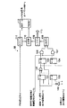
上記PLL回路72は、図4に示すように、基準パターン信号発生回路81、セレクタ回路82、83、位相比較器84、スイッチSW1、SW2、SW3、加算抵抗R1、R2、R3、ループフィルタ(平滑化回路)85、電圧制御発振器(VCO)86、分周器87、定常位相偏差補正値生成回路88、およびローパスフィルタ(平滑化回路)89により構成されている。
【0056】
基準パターン信号発生回路81は、図示しない発振器からのクロックに基づいて光ディスク1に記録されている同期コードと同様な4Tが連続するチャネル信号を基準パターン信号として発生するものである。この基準パターン信号はセレクタ回路82へ出力される。
【0057】
セレクタ回路82は、基準パターン信号発生回路81からの基準パターン信号と上記2値化回路71からの2値化信号とが供給され、上記CPU50から供給される定常位相偏差補正制御信号が供給されている間、基準パターン信号を出力し、それ以外の時、2値化信号を出力するようになっている。このセレクタ回路82からの信号は位相比較器84、定常位相偏差補正値生成回路88に出力される
セレクタ回路83は、電圧制御発振器86からのチャネルクロックと分周器87からのチャネルクロックをn分周したクロックとが供給され、上記CPU50から供給される定常位相偏差補正制御信号が供給されている間、分周器87からのクロックを出力し、それ以外の時、電圧制御発振器86からのチャネルクロックを出力するようになっている。このセレクタ回路83からのクロックは位相比較器84、定常位相偏差補正値生成回路88に出力される
上記位相比較器84は、上記セレクタ回路82からの2値化信号(再生信号)と上記セレクタ回路82からのチャネルクロックとの位相を比較し、その比較した位相差に比例したパルス幅を持つ信号としてオフセット付き位相誤差検出パルスとオフセット除去パルスと、チャネルクロックに同期したチャネルデータを出力する。この位相比較器84からのオフセット付き位相誤差検出パルスはオン、オフパルスとしてスイッチSW1、SW3に出力され、オフセット除去パルスはオン、オフパルスとしてスイッチSW2に出力され、チャネルデータは復調回路73に出力される。
【0058】
位相比較器84は、図4に示すように、2個のフリップフロップ回路(FF回路)91、92とEOR(エックスクルーシブオア)回路93とENR(エックスクルーシブノア)回路94とにより構成される。上記セレクタ回路82からの2値化信号は、FF回路91のデータ入力端とEOR回路93の一端に供給され、上記セレクタ回路82からのチャネルクロックは、FF回路91、92のクロック入力端に供給される。FF回路91のセット出力はEOR回路93の他端とENR回路94の一端に供給され、FF回路92のセット出力はENR回路94の他端に供給される。
【0059】
FF回路91のセット出力はチャネルデータとして出力され、EOR回路93からの出力信号はオフセット付き位相誤差検出パルスとなっており、ENR回路94からの出力信号はオフセット除去パルスとなっている。
【0060】
スイッチSW1は、オフセット付き位相誤差検出パルスにより制御される。オフセット付き位相誤差検出パルスがHレベルの期間、スイッチSW1がオンとなり、加算抵抗R1の逆数に比例した量の正極性の電流がループフィルタ85に流れる。スイッチSW2は、オフセット除去パルスにより制御される。オフセット除去パルスがLレベルの期間、スイッチSW2がオンとなりループフィルタ85に加算抵抗R2の逆数に比例した量の負極性の電流が流れる。
【0061】
ループフィルタ85は、オペアンプ85aとコンデンサC1と抵抗R4で構成されている。点Cには、点Aの電位をVA、点Bの電位をVBとすると、VC=(VA+VB)/2となる電圧VCが印加される。点Dの電位VDは、ループフィルタ85の動作によりVD=VCである。ループフィルタ85の出力電圧は、入力電荷の総和量に比例する。この例におけるVCO86は、出力信号の周波数が入力制御電圧に逆比例する。したがって、ループフィルタ85の出力電圧が上昇すればVCO86の出力信号の周波数は低下し、ループフィルタ85の出力電圧が低下すればVCO86の出力信号の周波数は上昇するようになっている。
【0062】
電圧制御発振器(VCO;voltage control oscillator)86は、ループフィルタ85から供給される信号の電圧値(アナログ値)に比例した周波数の2値のクロック信号(チャネルクロック)を出力するものである。
【0063】
この電圧制御発振器86のチャネルクロックは、セレクタ回路83に供給されるとともに、分周器87を介してセレクタ回路83に供給され、さらに復調回路73に出力される。
【0064】
上記分周器87は、電圧制御発振器86のチャネルクロックをn(2)分周するものである。VCO86の出力をn分周する理由は、クロックのデューティ比を保証するためである。
【0065】
上記定常位相偏差補正値生成回路88は、図示しない発振器からのPWM(パルスワイズモジュレーション)生成クロックと基準パターン信号発生回路81からセレクタ回路82を介して供給される基準パターン信号とVCO86からのチャネルクロックを分周器87でn分周してセレクタ回路82を介して供給されるクロックと上記CPU50から供給される定常位相偏差補正制御信号とに基づいて、定常位相偏差の補正値を生成するものである。
【0066】
ローパスフィルタ89は、抵抗R5とコンデンサC2からなる積分器により構成される。
上記定常位相偏差補正値生成回路88は、図5に示すように、インバータ100、FF回路101、102、103、104、EOR回路105、アンド回路106、107、アップダウンカウンタ108、レジスタ109、比較器110、カウンタ111、FF回路112、およびインバータ113により構成されている。
【0067】
上記FF回路101、102のデータ入力端には、上記セレクタ回路82から供給される図6の(c)に示す基準パターン信号が供給され、上記FF回路101のクロック入力端には、図6の(a)に示すVCO86からのチャネルクロックを2分周した図6の(b)に示す上記セレクタ回路83からのクロックがインバータ100により反転されて供給され、上記FF回路102のクロック入力端には、上記セレクタ回路83からのクロックが供給される。
【0068】
上記FF回路101、102のセット出力(図6の(e)(d)に示す)は、EOR回路105に供給され、このEOR回路105の出力(図6の(f)に示す)は、上記FF回路103、104のデータ入力端に供給される。
【0069】
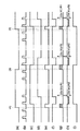
上記FF回路103のクロック入力端には、上記セレクタ回路83からのクロックがインバータ100により反転されて供給され、上記FF回路104のクロック入力端には、上記セレクタ回路83からのクロックが供給される。上記FF回路104、105のセット出力(図6の(h)(g)に示す)は、それぞれアンド回路106、107の一端に供給され、アンド回路106、107の他端には、上記CPU50から供給される定常位相偏差補正制御信号(図6の(i)に示す)が供給される。アンド回路106からの図6の(k)に示すダウンカウント出力とアンド回路107からの図6の(j)に示すアップカウント出力は、アップダウンカウンタ108に供給される。アップダウンカウンタ108のカウント値(図6の(l)、図7の(d)に示す)はレジスタ109に供給される。このレジスタ109にはカウンタ111からの図7の(c)に示すリップルキャリーン信号をインバータ113で反転した信号が供給される。
【0070】
レジスタ109は、インバータ113からの信号により、アップダウンカウンタ108のカウント値を保持し、この保持した図7の(e)に示すカウント値は比較器110へ出力される。
【0071】
カウンタ111には、バイナリカウンタであり、図示しない発振器のクロックを分周した図7の(a)に示すPWM生成クロックが供給される。このカウンタ111は、8ビットのバイナリカウンタであり、供給されるクロックにより巡回カウントを行い、このカウント値(図7の(b)に示す)が比較器110へ出力され、カウント値がFFhとなるごとに出力するリップルキャリーン信号はFF回路112のセット入力端に供給されるとともに、インバータ113を介してレジスタ109のリセット入力端に供給される。
【0072】
比較器110は、レジスタ109からのカウント値とカウンタ111からのカウント値とをビット比較し、一致している場合に図7の(f)に示す一致信号がFF回路112のリセット入力端に供給される。FF回路112のセット出力は図7の(g)に示すPWM信号(定常位相偏差補正値)に変調されてローパスフィルタ89に出力される。
【0073】
上記インバータ100、FF回路101、102、103、104、EOR回路105により、位相差極性信号検出回路が構成され、アンド回路106、107、アップダウンカウンタ108、レジスタ109、比較器110、カウンタ111、FF回路112により、PWM回路が構成されている。
【0074】
すなわち、図6の(a)から(l)は、図5の各部の動作タイミングであり、アップダウンカウンタ108までの動作を示す。
図6の(a)は、VCO86からのチャネルクロックで、デューティーが50%でない場合を示している。
【0075】
図6の(b)は、VCO86からのチャネルクロックを分周器87により2分周した信号で、クロックに相当する。
図6の(c)は、基準パターン信号に相当する。時間軸前半は相対的に図6の(b)のクロックがが遅れるように定常位相偏差が生じている場合を、後半は相対的に図6の(b)のクロックがが進んでいるように定常位相偏差が生じている場合を示す。
【0076】
図6の(d)は、基準パターン信号をクロックの立ち上がりにFF回路102で同期化した信号を示す。
図6の(e)は、基準パターン信号をクロックの立ち下がりにFF回路101で同期化した信号を示す。
【0077】
図6の(f)は、FF回路101のセット出力とFF回路102のセット出力のEOR回路105による排他的論理和を示す。
図6の(g)は、EOR回路105による排他的論理和出力をクロックの立ち上がりにFF回路104で同期化した信号であり、相対的にクロックが遅れていることを示す。
【0078】
図6の(h)は、EOR回路105による排他的論理和出力をクロックの立ち下がりにFF回路103で同期化した信号であり、相対的にクロックが進んでいることを示す。
【0079】
図6の(i)は、定常位相偏差補正制御信号で、Hレベルで定常位相偏差補正値の生成状態を示す。Lレベルでは、図6の(k)(j)に示す、アンド回路106、107の出力がLレベルに固定になり、アップダウンカウンタ108の動作が停止(ホールド)となる。
【0080】
図6の(j)は、FF回路107のセット出力と定常位相偏差補正制御信号を論理積した結果を示し、アップダウンカウンタ108のアップカウント信号となる。
【0081】
図6の(k)は、FF回路106のセット出力と定常位相偏差補正制御信号を論理積した結果を示し、アップダウンカウンタ108のダウンカウント信号となる。
【0082】
図7の(a)は、カウンタ111へのPWM生成クロックで、所定の周波数を持ち、例えばクロック生成回路で生成される。
図7の(b)は、カウンタ111の出力値を示し、この例では8ビットカウンタの出力値を示す。
【0083】
図7の(c)は、カウンタ111のリップルキャリー信号で、カウンタ出力値がFFhでHレベルとなる。
図7の(d)は、アップダウンカウンタ108の出力値を示す。
【0084】
図7の(e)は、アップダウンカウンタ108の出力値をカウンタ111のリップルキャリー信号の立ち下がりでラッチした信号で、レジスタ109の出力となる。
【0085】
図7の(f)は、カウンタ111の出力値とレジスタ109の出力が一致するとHレベルとなる比較器110の出力となる。
図7の(g)は、カウンタ111のリップルキャリー信号でセットし、比較器110からの一致信号によりリセットするFF回路112からのセット出力としてのPWM信号を示す。
【0086】
この実施の形態では、通常動作時の前に、定常位相偏差補正動作を行う。定常位相偏差補正動作時は、定常位相偏差補正制御信号がHレベルとなり、セレクタ回路82は基準パターン信号を出力し、セレクタ回路83はVCO86の出力をn分周した信号を出力する。したがって、定常位相偏差補正動作時において、位相比較器84は、基準パターン信号とVCO86の出力をn分周した信号の位相を比較する。VCO86の出力をn分周する理由は、再生クロックのデューティ比を保証するためである。定常位相偏差補正制御信号がHレベルなので、アップダウンカウンタ108は、カウンタ動作を実行する。
【0087】
図8の(a)から(e)に、定常位相偏差補正動作時における定常位相偏差の補正動作の様子を示す。図8の(a)は時点(1)〜(3)における基準パターン信号を、図8の(b)は時点(1)〜(3)における再生クロックを、図8の(c)はアップダウンカウンタ108の出力値を、図8の(d)はローパスフィルタ89の出力電圧を、図8の(e)はループフィルタ85への入力電流波形を示す。図8の(e)の斜線部は、加算抵抗R3を介して加算される補正電流分を示す。
【0088】
図8の時点(1)は、定常位相偏差の補正動作を開始していない初期状態である。図8の(a)および(b)は、時点(1)において、基準パターン信号と再生クロックの間に定常位相偏差が存在し、基準パターン信号は再生クロックに対して位相が進んでいる事を示す。図8の(c)および(d)は、時点(1)において、それぞれの値が初期値である事を示す。初期状態において、加算抵抗アップダウンカウンタ108の出力は、ローパスフィルタ89の出力電圧がVCとなる値である。点Dの電位VDは、VD=VCとなるようにループフィルタ85により制御されているので、スイッチSW3がオン状態になっても、加算抵抗R3には加算電流が流れない。図8の(e)は、時点(1)において、加算抵抗R3を介して加算される補正電流が零である事を示す。ループフィルタは、オフセット付き位相誤差検出パルスとオフセット除去パルスによって制御され、定常位相偏差は除去されない。
【0089】
図8の時点(2)は、定常位相偏差の補正動作を開始後、アップダウンカウンタ108が収束していない状態である。図8の(a)および(ロ)は、図8の時点(2)において、基準パターン信号と再生クロックの位相誤差が、アップダウンカウンタ108の出力に基づいて補正されている事を示す。図8の時点(2)において、基準パターン信号と再生クロックk位相誤差は、完全には補正されていない。図8の(c)および(d)は、時点(2)において、アップダウンカウンタ108の出力値は収束点に向かって増加し、ローパスフィルタ89の出力電圧は、アップダウンカウンタ108の出力値に比例して増加している事を示す。スイッチSW3がオン状態の時、加算抵抗R3には、ローパスフィルタ89の出力電圧の増加分に比例した値の正極性の電流が流れる。図8の(e)は、時点(2)において、補正電流分が加算されて、ループフィルタ85に入力される様子を示す。
【0090】
図8の時点(3)では、定常位相偏差が補正された状態である。図8の(a)および(b)は、時点(3)において、基準パターン信号と再生クロックの位相差が零である事を示す。図8の(c)および(d)は、時点(3)において、アップダウンカウンタ108の出力値とローパスフィルタ89の出力電圧が収束している事を示す。図8の時点(3)において、アップダウンカウンタ108の出力値およびローパスフィルタ89の出力電圧は、定常位相偏差を補正する値となつている。スイッチSW3がオン状態の時、加算抵抗R3には、定常位相偏差を補正する値の電流が流れる。図8の(e)は、時点(3)において、定常位相偏差を補正する値の補正電流が加算されて、ループフィルタ85に入力される様子を示す。
【0091】
図8の時点(3)におけるアップダウンカウンタ108の出力値は、定常位相偏差を補正する値となっているので、この時点でのアップダウンカウンタ108の出力値を定常位相偏差補正制御信号により保持する。
【0092】
通常動作時には、定常位相偏差補正制御信号がLレベルとなり、セレクタ回路82は2値化信号を出力し、セレクタ回路83はVCO86の出力信号を出力する。したがって、通常動作時において、位相比較器は、2値化信号とVCO86の出力信号の位相を比較する。アップダウンカウンタ108は、定常位相偏差補正動作時のカウンタ値を保持している。オフセット付き位相誤差検出パルスがHレベルの期間に、定常位相偏差補正動作時に保持したカウンタ出力値より生成した補正電流をループフィルタ85に入力して、定常位相偏差を補正する。
【0093】
次に、上記のような構成において、上記CPU50から供給される定常位相偏差補正制御信号が供給されていない場合のPLL回路72の動作を、図9の(a)から(i)に示すタイミングチャートを用いて説明する。この場合、2値化回路71からの2値化信号がセレクタ回路82を介して位相比較器84に供給され、電圧制御発振器86のチャネルクロックがセレクタ回路82を介して位相比較器84に供給される。また、後述する定常位相偏差の補正値に基づく、ローパスフィルタ89からの出力がループフィルタ85に加算されて、定常位相偏差が補正されているものとする。
【0094】
図9の(a)は2値化信号を示し、図9の(b)は再生クロックを示し、図9の(c)はFF回路91の出力信号を示し、図9の(d)はFF回路92の出力信号を示し、図9の(e)はオフセット付き位相誤差検出パルスを示し、図9の(f)はオフセット除去パルスを示し、図9の(g)は抵抗R1を流れる電流の波形を示し、図9の(h)は抵抗R2を流れる電流の波形を示す。
【0095】
図9の時点(1)においては、2値化信号とチャネルクロックは位相が同期しており、オフセット付き位相誤差検出パルスとオフセット除去パルスのパルス幅比は1:2である。加算抵抗R1とR2の抵抗値の比を1:2とすると、図9の(g)の斜線部の面積と図9の(h)の斜線部の面積が等しくなる。すなわち、それぞれのパルスによってループフィルタ85に供給される電荷量の絶対値が等しくなる。それそれのパルスによってループフィルタ85に供給される電荷の極性は逆であるため、結果としてループフィルタ85の出力は変化しない。VCO8686の入力電圧が変化しないため、チャネルクロックの周波数も変化せず、2値化信号とチャネルクロックの位相は同期した状態を保持する。
【0096】
図9の時点(2)では、2値化信号がチャネルクロックに対して位相が進んでいる。オフセット付き位相誤差検出パルスのパルス幅は、時点(1)と比較して位相誤差分だけ増加している。加算抵抗R1とR2の抵抗値の比が1:2の場合、図9の(g)の斜線部の面積が図9の(h)の斜線部の面積より大きくなる。すなわち、オフセット付き位相誤差検出パルスによってループフィルタ85に供給される電荷量の絶対値が、オフセット除去パルスによって供給される値より多くなる。その結果、ループフィルタ85の出力電圧が低下するため、VCO8686の出力信号の周波数が高くなり、2値化信号とチャネルクロックの位相差分が除去される。
【0097】
図9の時点(3)では、2値化信号がチャネルクロックに対して位相が遅れている。オフセット付き位相誤差検出パルスのパルス幅は、時点(1)と比較して位相誤差分だけ減少している。加算抵抗R1とR2の抵抗値の比が1:2の場合、図9の(g)の斜線部の面積が図9の(h)の斜線部の面積より小さくなる。すなわち、オフセット付き位相誤差検出パルスによってループフィルタ85に供給される電荷量の絶対値が、オフセット除去パルスによって供給される値より少なくなる。その結果、ループフィルタ85の出力電圧が上昇するため、VCO86の出力信号の周波数が低くなり、2値化信号と再生クロックの位相差分が除去される。
【0098】
なお、上記例では、オフセット付き位相誤差検出パルスがハイレベルの際に、定常位相偏差補正値が加算される場合、つまりスイッチSW1とSW3とが同時にオンされる場合について説明したが、これに限らず、補正信号生成ループつまり定常位相偏差補正値生成回路88とローパスフィルタ89の極性が反転している場合、オフセット除去パルスがハイレベルの際に、定常位相偏差補正値が加算される、つまりスイッチSW2とSW3とが同時にオンされる場合も同様に実施できる。
【0099】
図10に第2の実施形態の構成図を示す。
この場合、データレートデータレート検出回路90が図4のPLL回路72に追加される。
【0100】
基準パターン信号発生回路81は、基準パターン信号を出力する。基準パターン信号は、例えば14T−4Tのような特定パターンと4Tが連続するパターンとで構成される。2値化信号には、基準パターン信号と同じ特定パターンが含まれる。
【0101】
データレート検出回路90には、セレクタ回路82の出力信号と再生クロックが入力される。データレート検出回路90では、セレクタ回路82の出力信号中に含まれている特定パターン(本例では、14T−4T)を検出し、再生クロック周期と検出された特定パターンの周期を相対比較する。
【0102】
比較した結果、再生クロック周期が特定パターンの周期に対して相対的に所定値以上に大きい(再生クロックの周波数が相対的に低い)と判断された場合は、所定輻のHレベルパルスを周波数制御信号として出力し、抵抗R4を介してループフィルタ85に注入する。これにより、再生クロック周波数は高められる。
【0103】
一方、再生クロック周期が特定パターンの周期に対して相対的に所定値以上に小さい(再生クロックの周波数が相対的に高い)と判断された場合は、所定幅のLレベルパルスを周波数制御信号として出力し、抵抗R4を介してループフィルタ85に注入する。
【0104】
これにより、再生クロック周波数は低められる。もし、再生クロック周期と特定パターンの周期との相対誤差が所定値以下であれば、周波数制御信号は出力されない。
【0105】
ここで、動作初期状態などにおける位相非同期状態などにおいてVCO86の出力信号周波数が入力信号のデータレートに対して大きく異なる場合、周波数制御信号によりVCO86の出力信号周波数(再生クロック周波数)は概ね入力信号データレート近傍に制御される。この周波数制御によりVCO86の出力信号周波数(再生クロック周波数)が、位相比較器84、ループフィルタ85、VCO86で構成される位相同期ループにおけるキャプチャレンジ内になると、前記位相同期ループの働きにより、VCO86は制御され、入力信号のデータレートに一致し、位相同期した再生クロックが得られる。
【0106】
データレート検出回路90の出力である周波数制御信号は、加算抵抗R4を介してループフィルタ85に入力される。データレート検出回路90は、位相同期ループ回路が引き込める範囲内に再生クロックの周波数を追い込むように、ループフィルタ85を制御する。
【0107】
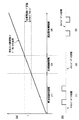
図11に周波数制御信号と再生クロックの周波数の関係を示す。図11の(a)は再生クロック周波数とデータレートとの比率と回路動作の関係を、図11の(b)は各動作時における周波数制御信号を示す。図11の(a)は、再生クロック周波数とデータレートとの比率が、位相同期ループ回路のキャプチャレンジ内にあれば、本回路は位相制御動作を行い、位相同期ループ回路のキャプチャレンジ外ならば、本回路は周波数制御動作を行う事を示す。
【0108】
それぞれの動作期間を(1)〜(3)とする。期間(1)と(3)は、再生クロックの周波数とデータレートとの比率が位相同期ループ回路のキャプチャレンジ範囲外である。期間(1)は再生クロックの周波数が位相同期ループ回路のキャプチャレンジより低い場合で、期間(3)は再生クロックの周波数が位相同期ループ回路のキャプチャレンジより高い場合である。期間(2)は、再生クロックの周波数とデータレートとの比率が位相同期ループ回路のキャプチャレンジ範囲内の場合である。
【0109】
図11の(b)は、各期間における周波数制御信号の様子を示す。期間(1)において、周波数制御信号は正極性のパルスとなる。期間(2)において、周波数制御信号はハイインピーダンス状態となる。期間(3)において、周波数制御信号は負極性のパルスとなる。
【0110】
期間(1)では、周波数制御信号によってループフィルタに正極性の電流が入力され、VCO86の出力信号の周波数が上昇する。その結果、再生クロックの周波数とデータレートとの比率か、位相同期ループ回路のキャプチャレンジに入る。期間(2)では、ループフィルタ85には電流が入力されないため、VCO86の出力信号の周波数が周波数制御信号によつて変化することはない。
【0111】
したがって、再生クロックの周波数とデータレートとの比率は、位相同期ループ回路のキャプチャレンジから外れない。期間(3)では、周波数制御信号によってループフィルタに負極性の電流が入力され、VCO86の出力信号の周波数は低下する。その結果、再生クロックの周波数とデータレートとの比率か、位相同期ループ回路のキャプチャレンジに入る。
【0112】
上記のような動作により、上記回路は、再生クロックの周波数が位相同期ループ回路のキャプチャレンジより外れている場合に、位相同期ループ回路が引き込める範囲内に再生クロックの周波数を追い込む。再生クロックの周波数が位相同期ループ回路のキャプチャレンジに入っている場合には、位相同期ループ回路が第1の実施形態と同様の動作をし、再生クロックと、2値化信号または基準パターン信号を位相同期させる。
【0113】
【発明の効果】
以上詳述したように、この発明によれば、定常位相偏差を除去した正確な再生クロックを生成することができる再生クロック生成回路を提供できる。
また、この発明によれば、正確な再生クロックに基づく正確な再生を行うことができないという欠点を除去するもので、正確な再生クロックに基づく正確な再生を行うことができる光ディスク装置を提供できる。
【図面の簡単な説明】
【図1】図1は、この発明の実施形態に係る光ディスクシステムの概略構成を示すブロック図。
【図2】図2は、図1に示した光ディスクの概略構成を示す平面図。
【図3】図3は、図1に示した光ディスクの概略構成を示す図。
【図4】図4は、図1に示したPLL回路の構成を示すブロック図。
【図5】図5は、図4に示した定常位相偏差補正値生成回路の構成を示すブロック図。
【図6】図6は、図5の各部の動作タイミングを示す図。
【図7】図7は、図5の各部の動作タイミングを示す図。
【図8】図8は、定常位相偏差補正動作時における定常位相偏差の補正動作の様子を示す図。
【図9】図9は、定常位相偏差補正制御信号が供給されていない場合のPLL回路の動作を示すタイミングチャート。
【図10】図10は、第2の実施態様のPLL回路の構成を示すブロック図。
【図11】図11は、第2の実施態様の周波数制御信号と再生クロックの周波数の関係を示す図。
【符号の説明】
1…光ディスク
10…メモリ
25…光学ヘッド
38…データ再生回路
50…CPU
71…2値化回路
72…PLL回路
81…基準パターン信号発生回路
88…定常位相偏差補正値生成回路
89…ローパスフィルタ
90…データレート検出回路[0001]
BACKGROUND OF THE INVENTION
The present invention relates to an optical disc apparatus that records data on an optical disc and reproduces data recorded on the optical disc, and a reproduction clock generation circuit that generates a reproduction clock used when reproducing data from the optical disc.
[0002]
[Prior art]
Recently, a digital video disc (DVD) has been developed as an optical disc of a large capacity recording medium, and an optical disc apparatus and an optical disc for recording and reproducing data recorded on the optical disc and reproducing data recorded on the optical disc. A reproduction-only optical disc apparatus for reproducing the data recorded on the disc has been developed.
[0003]
In such an optical disc apparatus, pits are formed by a mark length recording (mark edge recording) system, and channel data is recorded.
In the above-described reproducing circuit in the optical disk apparatus, a reproducing signal (after amplification) from the detector of the optical head is binarized by a comparator, and a reproducing clock, that is, a channel clock is generated by this binarized signal (reproducing clock). Generation circuit, phase synchronization circuit), and channel data, that is, reproduction data is demodulated based on a channel clock generated by the PLL circuit.
[0004]
The PLL circuit compares the phase of the supplied binarized signal with the channel clock generated by the VCO, and outputs a signal having a pulse width proportional to the compared phase difference and channel data. The first switch that is turned on and off by the offset phase error detection pulse from the phase comparator, the second switch that is turned on and off by the offset removal pulse from the phase comparator, and the first switch being turned on An amount of positive polarity current proportional to the reciprocal of the addition resistor R1 flows, and an amount of negative polarity current proportional to the reciprocal of the addition resistor R2 flows when the second switch is turned on to smooth the output of the phase comparator. A loop filter and a binary clock signal (channel clock) with a frequency proportional to the voltage value (analog value) output from the loop filter are output. It is composed of; (voltage control oscillator VCO) controlled oscillator.
[0005]
In the PLL circuit as described above, when the circuit is actually manufactured, it is very difficult to set the resistance value ratio of the two addition resistors R1 and R2 to a predetermined value without error. The error in the resistance value ratio causes a steady phase deviation.
[0006]
For example, it is assumed that the phase of the binarized signal is advanced by 10% for one period of the channel clock with respect to the channel clock. The pulse width ratio between the phase error detection pulse with offset and the offset removal pulse is 1.2: 2. If the ratio of the resistance values of the addition resistors R1 and R2 is 1: 2, the ratio of the total positive current value to the total negative current value is 1.2: 1. As a result, the output voltage of the loop filter is The phase difference between the binarized signal and the channel clock is removed. If the ratio of the resistance values of the addition resistors R1 and R2 is 1.2: 2, the ratio of the total positive current value to the total negative current value is 1: 1, and as a result, the output voltage of the loop filter changes. do not do. Since the frequency of the channel clock does not change, the state where the phase of the binarized signal is advanced with respect to the phase of the channel clock is maintained.
[0007]
When the ratio of the addition resistance values is an incorrect value as described above, there is a phase deviation between the binarized signal and the channel clock in the steady state. If there is a steady phase deviation between the binarized signal and the channel clock, the data cancellation phase is not the phase best point, and therefore errors due to jitter increase when the binarized signal includes jitter.
[0008]
In addition to the case where the addition resistance value ratio is incorrect, when the current value flowing through the addition resistor changes due to the internal resistance of the two switches, or the comparison voltage value supplied to the comparator in the loop filter is the addition resistor R1. A steady phase deviation occurs when 1/2 of the difference between the voltage applied to and the voltage value applied to the adding resistor R2 is not satisfied.
[0009]
Therefore, the PLL circuit as described above has a drawback that an accurate channel clock cannot be generated due to a steady phase deviation. As a result, the channel data based on the channel clock is not accurate.
For this reason, an optical disc apparatus that reproduces data using such a PLL circuit has a drawback that accurate reproduction cannot be performed.
[0010]
[Problems to be solved by the invention]
An object of the present invention is to provide a reproduction clock generation circuit capable of generating an accurate reproduction clock from which a stationary phase deviation is removed, in order to eliminate the disadvantage that an accurate reproduction clock cannot be generated due to the stationary phase deviation. Yes.
[0011]
An object of the present invention is to provide an optical disk apparatus that eliminates the disadvantage that accurate reproduction based on an accurate reproduction clock cannot be performed, and that can perform accurate reproduction based on an accurate reproduction clock. .
[0012]
[Means for Solving the Problems]
The regenerated clock generation circuit of the present invention generates a regenerated clock synchronized with the received signal, compares the phase of the received signal with the generated regenerated clock, and adds an offset proportional to the phase difference based on the comparison result. First generation means for generating the first detection pulse and the second detection pulse from which the offset is removed, and a positive current for a period corresponding to the first detection pulse generated by the first generation means And a negative current flows for a period corresponding to the second detection pulse generated by the first generation means, thereby smoothing a signal corresponding to the phase difference in the first generation means. 1 smoothing circuit, a clock generation means for generating a reproduction clock having a frequency corresponding to the output of the first smoothing circuit, the reception signal and the clock generation means. Generated by a second generation means for generating a correction signal for the stationary phase deviation by the reproduction clock, a second smoothing circuit for smoothing the correction signal by the second generation means, and the first generation means. Adding means for adding the output of the second smoothing circuit to the output of the first smoothing circuit for a period corresponding to the first detection pulse or the second detection pulse.
[0013]
An optical disk apparatus according to the present invention reproduces data recorded on an optical disk. An optical head for reproducing data from the optical disk and a reproduction clock based on a reproduction signal reproduced by the optical head. And a demodulating means for demodulating a reproduction signal reproduced by the optical head into reproduction data based on the reproduction clock generated by the reproduction clock generation circuit. The reproduction clock generation circuit comprises: The first detection pulse with an offset proportional to the phase difference and the second detection with the offset removed based on a comparison result between the phase of the reproduction signal reproduced by the optical head and the generated reproduction clock First generation means for generating a pulse, and a first detection pulse generated by the first generation means A positive current flows for a period of time, and a negative current flows for a period of time corresponding to the second detection pulse generated by the first generation unit, thereby causing a phase difference in the first generation unit. Generated by the first smoothing circuit for smoothing the corresponding signal, clock generation means for generating a reproduction clock having a frequency corresponding to the output of the first smoothing circuit, the reproduction signal and the clock generation means A second generation means for generating a correction signal for the steady phase deviation by using the reproduced clock; a second smoothing circuit for smoothing the correction signal by the second generation means; and the first generation means. It comprises an adding means for adding the output of the second smoothing circuit to the output of the first smoothing circuit for a period corresponding to the generated first detection pulse or second detection pulse.
[0018]
DETAILED DESCRIPTION OF THE INVENTION
An optical disk system showing a first embodiment of the present invention will be described below with reference to the drawings.
An
[0019]
The
[0020]
As shown in FIGS. 2 and 3, the
[0021]
The
The lead-out
[0022]
As shown in FIG. 3, the
[0023]
In the
[0024]
The relationship between the speed data as the rotational speed and the number of sectors per track for each of the
[0025]
As shown in FIGS. 2 and 3, the tracks in the
[0026]
The ECC block is composed of 16 sectors in which 2K bytes of data are recorded, and each sector has 4 bytes (32 bits) of sector ID (identification data) 1 to ID 16 as an address data. A horizontal ECC (error correction code) 1 as an error correction code for reproducing data recorded in the ECC block, which is given to the main data (sector data) together with the detection code (IED: ID error detection code), and The vertical ECC2 is recorded. The
[0027]
Each sector is composed of 172 bytes and 12 rows of data, and each row (line) is given a horizontal ECC1 of 10 bytes and a vertical ECC2 of one row of 182 bytes. Has been. Accordingly, the
[0028]
When the ECC block is recorded on the
[0029]
As shown in FIG. 2, a
[0030]
Each
[0031]
In FIG. 1, the
[0032]
Recording of data on the
[0033]
A speed detector 29 is connected to the linear
In addition, a permanent magnet (not shown) is provided in the fixed portion of the
[0034]
An
[0035]
Further, the
[0036]
The
[0037]
The laser light generated from the
[0038]
The
The output signal of the
[0039]
The output signal of the
[0040]
The output signal of the
[0041]
The output signal of the
[0042]
The track drive signal output from the
[0043]
A signal obtained by adding the output signals from the
[0044]
The reproduction data reproduced by the
[0045]
When the
[0046]
In addition, a
[0047]
The
[0048]
The
[0049]
Further, the
[0050]
The
[0051]
The
[0052]
As shown in FIG. 1, the
The binarization circuit 71 is a circuit that binarizes the output signal from the
[0053]
The
While the steady phase deviation correction control signal supplied from the
[0054]
The
[0055]
As shown in FIG. 4, the
[0056]
The reference pattern signal generation circuit 81 generates, as a reference pattern signal, a channel signal having a continuous 4T similar to the synchronization code recorded on the
[0057]
The
The
The phase comparator 84 compares the phase of the binarized signal (reproduced signal) from the
[0058]
As shown in FIG. 4, the phase comparator 84 includes two flip-flop circuits (FF circuits) 91 and 92, an EOR (exclusive OR)
[0059]
The set output of the
[0060]
The switch SW1 is controlled by a phase error detection pulse with an offset. While the phase error detection pulse with offset is at the H level, the switch SW1 is turned on, and an amount of positive current proportional to the reciprocal of the addition resistor R1 flows through the
[0061]
The
[0062]
A voltage controlled oscillator (VCO) 86 outputs a binary clock signal (channel clock) having a frequency proportional to the voltage value (analog value) of the signal supplied from the
[0063]
The channel clock of the voltage controlled
[0064]
The
[0065]
The steady phase deviation correction
[0066]
The low-pass filter 89 is configured by an integrator including a resistor R5 and a capacitor C2.
As shown in FIG. 5, the steady phase deviation correction
[0067]
The reference pattern signal shown in FIG. 6C supplied from the
[0068]
The set outputs (shown in (e) and (d) of FIG. 6) of the
[0069]
The clock from the
[0070]
The
[0071]
The counter 111 is a binary counter, and is supplied with a PWM generation clock shown in FIG. 7A obtained by dividing the clock of an oscillator (not shown). The counter 111 is an 8-bit binary counter, and performs a cyclic count using a supplied clock. The count value (shown in FIG. 7B) is output to the
[0072]
The
[0073]
The
[0074]
That is, (a) to (l) in FIG. 6 are the operation timings of the respective units in FIG.
FIG. 6A shows a case where the channel clock is from the
[0075]
6B shows a signal obtained by frequency-dividing the channel clock from the
FIG. 6C corresponds to the reference pattern signal. In the first half of the time axis, a steady phase deviation occurs so that the clock in FIG. 6B is relatively delayed, and in the second half, the clock in FIG. 6B is relatively advanced. The case where a stationary phase deviation has occurred is shown.
[0076]
FIG. 6D shows a signal obtained by synchronizing the reference pattern signal with the rising edge of the clock by the
FIG. 6E shows a signal obtained by synchronizing the reference pattern signal with the falling edge of the clock by the
[0077]
FIG. 6F shows the exclusive OR of the set output of the
(G) of FIG. 6 is a signal obtained by synchronizing the exclusive OR output from the
[0078]
(H) in FIG. 6 is a signal obtained by synchronizing the exclusive OR output from the
[0079]
(I) of FIG. 6 is a steady phase deviation correction control signal, and shows a generation state of a steady phase deviation correction value at the H level. At the L level, the outputs of the AND
[0080]
(J) of FIG. 6 shows the result of logical product of the set output of the
[0081]
(K) in FIG. 6 shows the result of logical product of the set output of the
[0082]
FIG. 7A shows a PWM generation clock to the counter 111, which has a predetermined frequency and is generated by, for example, a clock generation circuit.
FIG. 7B shows the output value of the counter 111, and in this example, the output value of the 8-bit counter.
[0083]
FIG. 7C shows a ripple carry signal of the counter 111. The counter output value becomes FFh and becomes H level.
FIG. 7D shows the output value of the up / down
[0084]
(E) of FIG. 7 is a signal obtained by latching the output value of the up / down counter 108 at the falling edge of the ripple carry signal of the counter 111 and is an output of the
[0085]
(F) in FIG. 7 is the output of the
(G) of FIG. 7 shows a PWM signal as a set output from the
[0086]
In this embodiment, the steady phase deviation correction operation is performed before the normal operation. During the steady phase deviation correction operation, the steady phase deviation correction control signal becomes H level, the
[0087]
FIGS. 8A to 8E show the state of the steady phase deviation correction operation during the steady phase deviation correction operation. 8A shows the reference pattern signal at time points (1) to (3), FIG. 8B shows the regenerated clock at time points (1) to (3), and FIG. 8D shows the output value of the
[0088]
The time point (1) in FIG. 8 is an initial state where the steady phase deviation correction operation is not started. 8A and 8B show that at the time point (1), there is a steady phase deviation between the reference pattern signal and the recovered clock, and the phase of the reference pattern signal is advanced with respect to the recovered clock. Show. (C) and (d) in FIG. 8 indicate that the respective values are initial values at the time point (1). In the initial state, the output of the addition resistor up / down
[0089]
The time point (2) in FIG. 8 is a state in which the up / down
[0090]
At the time (3) in FIG. 8, the steady phase deviation is corrected. (A) and (b) of FIG. 8 show that the phase difference between the reference pattern signal and the reproduction clock is zero at time (3). (C) and (d) of FIG. 8 show that the output value of the up / down
[0091]
Since the output value of the up / down counter 108 at the time (3) in FIG. 8 is a value for correcting the steady phase deviation, the output value of the up / down counter 108 at this time is held by the steady phase deviation correction control signal. To do.
[0092]
During normal operation, the steady phase deviation correction control signal becomes L level, the
[0093]
Next, in the configuration as described above, the operation of the
[0094]
9 (a) shows the binarized signal, FIG. 9 (b) shows the recovered clock, FIG. 9 (c) shows the output signal of the
[0095]
At time (1) in FIG. 9, the phase of the binarized signal and the channel clock is synchronized, and the pulse width ratio between the offset phase error detection pulse and the offset removal pulse is 1: 2. If the ratio of the resistance values of the addition resistors R1 and R2 is 1: 2, the area of the hatched portion in FIG. 9G and the area of the hatched portion in FIG. That is, the absolute value of the amount of charge supplied to the
[0096]
At time (2) in FIG. 9, the phase of the binarized signal is advanced with respect to the channel clock. The pulse width of the phase error detection pulse with offset is increased by the phase error compared to the time point (1). When the ratio of the resistance values of the addition resistors R1 and R2 is 1: 2, the area of the shaded portion in (g) of FIG. 9 is larger than the area of the shaded portion in (h) of FIG. That is, the absolute value of the amount of charge supplied to the
[0097]
At the time (3) in FIG. 9, the phase of the binarized signal is delayed with respect to the channel clock. The pulse width of the phase error detection pulse with offset is reduced by the phase error compared to the time point (1). When the ratio of the resistance values of the addition resistors R1 and R2 is 1: 2, the area of the shaded portion in (g) of FIG. 9 is smaller than the area of the shaded portion in (h) of FIG. That is, the absolute value of the amount of charge supplied to the
[0098]
In the above example, the case where the steady phase deviation correction value is added when the offset phase error detection pulse is at the high level, that is, the case where the switches SW1 and SW3 are simultaneously turned on has been described. First, when the polarity of the correction signal generation loop, that is, the stationary phase deviation correction
[0099]
FIG. 10 shows a configuration diagram of the second embodiment.
In this case, a data rate data
[0100]
The reference pattern signal generation circuit 81 outputs a reference pattern signal. The reference pattern signal is composed of a specific pattern such as 14T-4T and a pattern in which 4T continues. The binarized signal includes the same specific pattern as the reference pattern signal.
[0101]
The data
[0102]
As a result of comparison, if it is determined that the recovered clock period is relatively larger than a predetermined value relative to the period of the specific pattern (the frequency of the recovered clock is relatively low), the H level pulse of the predetermined radiation is frequency controlled. It outputs as a signal and injects into the
[0103]
On the other hand, when it is determined that the reproduction clock cycle is relatively smaller than a predetermined value with respect to the cycle of the specific pattern (the frequency of the reproduction clock is relatively high), an L level pulse having a predetermined width is used as a frequency control signal. Is output and injected into the
[0104]
Thereby, the reproduction clock frequency is lowered. If the relative error between the reproduction clock period and the specific pattern period is equal to or less than a predetermined value, the frequency control signal is not output.
[0105]
Here, when the output signal frequency of the
[0106]
The frequency control signal that is the output of the data
[0107]
FIG. 11 shows the relationship between the frequency control signal and the frequency of the recovered clock. FIG. 11A shows the relationship between the ratio between the reproduction clock frequency and the data rate and the circuit operation, and FIG. 11B shows the frequency control signal at each operation. (A) of FIG. 11 shows that if the ratio between the reproduction clock frequency and the data rate is within the capture range of the phase-locked loop circuit, this circuit performs the phase control operation, and if the ratio is outside the capture range of the phase-locked loop circuit. This circuit shows that the frequency control operation is performed.
[0108]
The respective operation periods are (1) to (3). In periods (1) and (3), the ratio between the frequency of the recovered clock and the data rate is outside the capture range of the phase-locked loop circuit. Period (1) is when the frequency of the recovered clock is lower than the capture range of the phase-locked loop circuit, and period (3) is when the frequency of the recovered clock is higher than the capture range of the phase-locked loop circuit. Period (2) is when the ratio between the frequency of the recovered clock and the data rate is within the capture range of the phase-locked loop circuit.
[0109]
FIG. 11B shows the state of the frequency control signal in each period. In the period (1), the frequency control signal is a positive pulse. In the period (2), the frequency control signal is in a high impedance state. In the period (3), the frequency control signal is a negative pulse.
[0110]
In the period (1), a positive current is input to the loop filter by the frequency control signal, and the frequency of the output signal of the
[0111]
Therefore, the ratio between the frequency of the recovered clock and the data rate does not deviate from the capture range of the phase locked loop circuit. In period (3), a negative current is input to the loop filter by the frequency control signal, and the frequency of the output signal of the
[0112]
With the above operation, when the frequency of the recovered clock is out of the capture range of the phase-locked loop circuit, the circuit drives the frequency of the recovered clock within a range that can be pulled in by the phase-locked loop circuit. When the frequency of the recovered clock is within the capture range of the phase locked loop circuit, the phase locked loop circuit operates in the same manner as in the first embodiment, and the recovered clock and the binarized signal or reference pattern signal are Synchronize the phase.
[0113]
【The invention's effect】
As described above in detail, according to the present invention, it is possible to provide a regenerated clock generation circuit capable of generating an accurate regenerated clock from which the steady phase deviation is removed.
In addition, according to the present invention, it is possible to provide an optical disc apparatus capable of performing accurate reproduction based on an accurate reproduction clock by eliminating the disadvantage that accurate reproduction based on an accurate reproduction clock cannot be performed.
[Brief description of the drawings]
FIG. 1 is a block diagram showing a schematic configuration of an optical disc system according to an embodiment of the present invention.
FIG. 2 is a plan view showing a schematic configuration of the optical disc shown in FIG. 1;
FIG. 3 is a diagram showing a schematic configuration of the optical disc shown in FIG. 1;
4 is a block diagram showing a configuration of the PLL circuit shown in FIG. 1. FIG.
FIG. 5 is a block diagram showing a configuration of a steady phase deviation correction value generation circuit shown in FIG. 4;
6 is a diagram illustrating operation timing of each unit in FIG. 5;
7 is a diagram illustrating operation timing of each unit in FIG. 5;
FIG. 8 is a diagram illustrating a state of a steady phase deviation correction operation during a steady phase deviation correction operation;
FIG. 9 is a timing chart showing the operation of the PLL circuit when a steady phase deviation correction control signal is not supplied.
FIG. 10 is a block diagram showing a configuration of a PLL circuit according to a second embodiment;
FIG. 11 is a diagram illustrating a relationship between a frequency control signal and a frequency of a reproduction clock according to the second embodiment;
[Explanation of symbols]
1 ... Optical disc
10 ... Memory
25. Optical head
38. Data reproduction circuit
50 ... CPU
71 ... Binary circuit
72 ... PLL circuit
81. Reference pattern signal generation circuit
88. Stationary phase deviation correction value generation circuit
89 ... Low-pass filter
90 ... Data rate detection circuit
Claims (2)
上記受信信号と生成した再生クロックとの位相を比較し、この比較結果に基づいて位相差に比例したオフセット付の第1の検出パルスとオフセットを除去した第2の検出パルスを生成する第1の生成手段と、
この第1の生成手段により生成される第1の検出パルスに応じた期間、正極性の電流が流れ、上記第1の生成手段により生成される第2の検出パルスに応じた期間、負極性の電流が流れることにより、上記第1の生成手段における位相差に応じた信号を平滑化する第1の平滑化回路と、
この第1の平滑化回路の出力に応じた周波数をもつ再生クロックを生成するクロック生成手段と、
上記受信信号と上記クロック生成手段により生成された再生クロックとにより定常位相偏差に対する補正信号を生成する第2の生成手段と、
この第2の生成手段による補正信号を平滑化する第2の平滑化回路と、
上記第1の生成手段により生成される第1の検出パルスあるいは第2の検出パルスに応じた期間、上記第2の平滑化回路の出力を上記第1の平滑化回路の出力に加算する加算手段と、
を具備したことを特徴とする再生クロック生成回路。In a recovered clock generation circuit that generates a recovered clock synchronized with a received signal,
The phase of the received signal and the generated recovered clock are compared, and a first detection pulse with an offset proportional to the phase difference and a second detection pulse with the offset removed are generated based on the comparison result Generating means;
A positive current flows for a period according to the first detection pulse generated by the first generation means, and a negative polarity for a period according to the second detection pulse generated by the first generation means. A first smoothing circuit for smoothing a signal corresponding to a phase difference in the first generation means by flowing a current;
Clock generating means for generating a recovered clock having a frequency corresponding to the output of the first smoothing circuit;
Second generation means for generating a correction signal for a stationary phase deviation from the received signal and the recovered clock generated by the clock generation means;
A second smoothing circuit for smoothing the correction signal by the second generation means;
Adding means for adding the output of the second smoothing circuit to the output of the first smoothing circuit for a period corresponding to the first detection pulse or the second detection pulse generated by the first generation means When,
A regenerated clock generation circuit comprising:
上記光ディスクに対してデータの再生を行う光学ヘッドと、An optical head for reproducing data from the optical disc;
この光学ヘッドにより再生される再生信号に基づいて再生クロックを生成する再生クロック生成回路と、A reproduction clock generation circuit for generating a reproduction clock based on a reproduction signal reproduced by the optical head;
この再生クロック生成回路により生成される再生クロックに基づいて、上記光学ヘッドにより再生される再生信号を再生データに復調する復調手段とを具備し、Demodulation means for demodulating a reproduction signal reproduced by the optical head into reproduction data based on a reproduction clock generated by the reproduction clock generation circuit;
上記再生クロック生成回路が、The reproduction clock generation circuit is
上記光学ヘッドにより再生される再生信号と生成した再生クロックとの位相を比較し、この比較結果に基づいて位相差に比例したオフセット付の第1の検出パルスとオフセットを除去した第2の検出パルスを生成する第1の生成手段と、The phase of the reproduction signal reproduced by the optical head and the generated reproduction clock are compared, and based on the comparison result, the first detection pulse with an offset proportional to the phase difference and the second detection pulse with the offset removed First generating means for generating
この第1の生成手段により生成される第1の検出パルスに応じた期間、正極性の電流が流れ、上記第1の生成手段により生成される第2の検出パルスに応じた期間、負極性の電流が流れることにより、上記第1の生成手段における位相差に応じた信号を平滑化する第1の平滑化回路と、A positive current flows for a period according to the first detection pulse generated by the first generation means, and a negative polarity for a period according to the second detection pulse generated by the first generation means. A first smoothing circuit that smoothes a signal corresponding to a phase difference in the first generation means by flowing current;
この第1の平滑化回路の出力に応じた周波数をもつ再生クロックを生成するクロック生成手段と、Clock generating means for generating a reproduction clock having a frequency corresponding to the output of the first smoothing circuit;
上記再生信号と上記クロック生成手段により生成される再生クロックとにより定常位相偏差に対する補正信号を生成する第2の生成手段と、Second generation means for generating a correction signal for a stationary phase deviation from the reproduction signal and the reproduction clock generated by the clock generation means;
この第2の生成手段による補正信号を平滑化する第2の平滑化回路と、A second smoothing circuit for smoothing the correction signal by the second generation means;
上記第1の生成手段により生成される第1の検出パルスあるいは第2の検出パルスに応じた期間、上記第2の平滑化回路の出力を上記第1の平滑化回路の出力に加算する加算手段とからなる、Adding means for adding the output of the second smoothing circuit to the output of the first smoothing circuit for a period corresponding to the first detection pulse or the second detection pulse generated by the first generation means Consisting of
ことを特徴とする光ディスク装置。An optical disc device characterized by the above.
Priority Applications (1)
| Application Number | Priority Date | Filing Date | Title |
|---|---|---|---|
| JP01966198A JP3987183B2 (en) | 1998-01-30 | 1998-01-30 | Reproduction clock generation circuit and optical disk apparatus |
Applications Claiming Priority (1)
| Application Number | Priority Date | Filing Date | Title |
|---|---|---|---|
| JP01966198A JP3987183B2 (en) | 1998-01-30 | 1998-01-30 | Reproduction clock generation circuit and optical disk apparatus |
Publications (2)
| Publication Number | Publication Date |
|---|---|
| JPH11213572A JPH11213572A (en) | 1999-08-06 |
| JP3987183B2 true JP3987183B2 (en) | 2007-10-03 |
Family
ID=12005440
Family Applications (1)
| Application Number | Title | Priority Date | Filing Date |
|---|---|---|---|
| JP01966198A Expired - Fee Related JP3987183B2 (en) | 1998-01-30 | 1998-01-30 | Reproduction clock generation circuit and optical disk apparatus |
Country Status (1)
| Country | Link |
|---|---|
| JP (1) | JP3987183B2 (en) |
Families Citing this family (1)
| Publication number | Priority date | Publication date | Assignee | Title |
|---|---|---|---|---|
| JP6064930B2 (en) * | 2014-03-07 | 2017-01-25 | ソニー株式会社 | Electrical / electronic equipment, circuits, and communication systems |
-
1998
- 1998-01-30 JP JP01966198A patent/JP3987183B2/en not_active Expired - Fee Related
Also Published As
| Publication number | Publication date |
|---|---|
| JPH11213572A (en) | 1999-08-06 |
Similar Documents
| Publication | Publication Date | Title |
|---|---|---|
| JP2954083B2 (en) | Information recording / reproducing medium, information recording / reproducing medium format device, and information recording / reproducing device | |
| JP3850600B2 (en) | Information recording disk and information recording apparatus | |
| JPH11120564A (en) | Optical disk device and optical disk reproducing method | |
| US7012865B2 (en) | Recording apparatus and recording method | |
| JP3492647B2 (en) | Information recording method and apparatus | |
| US7319645B2 (en) | Recording apparatus and recording method for recording data to a rewritable recording medium, and rewritable recording medium | |
| JP2685478B2 (en) | Information recording / reproducing method, information recording carrier, and information recording / reproducing apparatus | |
| JP3987183B2 (en) | Reproduction clock generation circuit and optical disk apparatus | |
| JP3875399B2 (en) | Tracking method for optical disk device and tracking method for DVD-RAM drive device | |
| JP3959147B2 (en) | Optical disc, optical disc playback apparatus, optical disc playback method, and optical disc recording method | |
| US7813231B2 (en) | Optical disc drive apparatus | |
| JP3959149B2 (en) | Optical disc, optical disc playback apparatus, optical disc playback method, and optical disc recording method | |
| JP3908347B2 (en) | Optical disc playback apparatus and optical disc playback method | |
| JPH1166726A (en) | Optical disk device | |
| JP3839917B2 (en) | Optical disk device | |
| JPH1064168A (en) | Data recorder | |
| JP3762028B2 (en) | Optical disc, optical disc playback apparatus, optical disc playback method, and optical disc recording method | |
| JP3762027B2 (en) | Optical disc, optical disc playback apparatus, optical disc playback method, and optical disc recording method | |
| JP3762029B2 (en) | Optical disc, optical disc playback apparatus, optical disc playback method, and optical disc recording method | |
| JP3959208B2 (en) | Optical disk apparatus and reproduction clock generation circuit | |
| JP2954130B2 (en) | Information recording / reproducing medium, information recording / reproducing medium format device, and information recording / reproducing device | |
| JPH10247325A (en) | Tracking method for data recorder and optical disk device, and signal processing method for optical disk device | |
| JP2954135B2 (en) | Information recording / reproducing medium, information recording / reproducing medium format device, and information recording / reproducing device | |
| JP2954133B2 (en) | Information recording / reproducing medium, information recording / reproducing medium format device, and information recording / reproducing device | |
| JP4694087B2 (en) | Disc recording / reproducing apparatus and reproducing method |
Legal Events
| Date | Code | Title | Description |
|---|---|---|---|
| A977 | Report on retrieval |
Free format text: JAPANESE INTERMEDIATE CODE: A971007 Effective date: 20061124 |
|
| A131 | Notification of reasons for refusal |
Free format text: JAPANESE INTERMEDIATE CODE: A131 Effective date: 20061212 |
|
| A521 | Written amendment |
Free format text: JAPANESE INTERMEDIATE CODE: A523 Effective date: 20070213 |
|
| TRDD | Decision of grant or rejection written | ||
| A01 | Written decision to grant a patent or to grant a registration (utility model) |
Free format text: JAPANESE INTERMEDIATE CODE: A01 Effective date: 20070710 |
|
| A61 | First payment of annual fees (during grant procedure) |
Free format text: JAPANESE INTERMEDIATE CODE: A61 Effective date: 20070712 |
|
| R150 | Certificate of patent or registration of utility model |
Free format text: JAPANESE INTERMEDIATE CODE: R150 |
|
| FPAY | Renewal fee payment (event date is renewal date of database) |
Free format text: PAYMENT UNTIL: 20100720 Year of fee payment: 3 |
|
| FPAY | Renewal fee payment (event date is renewal date of database) |
Free format text: PAYMENT UNTIL: 20110720 Year of fee payment: 4 |
|
| FPAY | Renewal fee payment (event date is renewal date of database) |
Free format text: PAYMENT UNTIL: 20120720 Year of fee payment: 5 |
|
| FPAY | Renewal fee payment (event date is renewal date of database) |
Free format text: PAYMENT UNTIL: 20130720 Year of fee payment: 6 |
|
| LAPS | Cancellation because of no payment of annual fees |